WO2019078366A1 - 距離画像測定装置及び距離画像測定方法 - Google Patents
距離画像測定装置及び距離画像測定方法 Download PDFInfo
- Publication number
- WO2019078366A1 WO2019078366A1 PCT/JP2018/039080 JP2018039080W WO2019078366A1 WO 2019078366 A1 WO2019078366 A1 WO 2019078366A1 JP 2018039080 W JP2018039080 W JP 2018039080W WO 2019078366 A1 WO2019078366 A1 WO 2019078366A1
- Authority
- WO
- WIPO (PCT)
- Prior art keywords
- distance
- mth
- control
- charge
- light
- Prior art date
- Legal status (The legal status is an assumption and is not a legal conclusion. Google has not performed a legal analysis and makes no representation as to the accuracy of the status listed.)
- Ceased
Links
Images









Classifications
-
- G—PHYSICS
- G01—MEASURING; TESTING
- G01S—RADIO DIRECTION-FINDING; RADIO NAVIGATION; DETERMINING DISTANCE OR VELOCITY BY USE OF RADIO WAVES; LOCATING OR PRESENCE-DETECTING BY USE OF THE REFLECTION OR RERADIATION OF RADIO WAVES; ANALOGOUS ARRANGEMENTS USING OTHER WAVES
- G01S17/00—Systems using the reflection or reradiation of electromagnetic waves other than radio waves, e.g. lidar systems
- G01S17/88—Lidar systems specially adapted for specific applications
- G01S17/89—Lidar systems specially adapted for specific applications for mapping or imaging
-
- G—PHYSICS
- G01—MEASURING; TESTING
- G01B—MEASURING LENGTH, THICKNESS OR SIMILAR LINEAR DIMENSIONS; MEASURING ANGLES; MEASURING AREAS; MEASURING IRREGULARITIES OF SURFACES OR CONTOURS
- G01B11/00—Measuring arrangements characterised by the use of optical techniques
- G01B11/14—Measuring arrangements characterised by the use of optical techniques for measuring distance or clearance between spaced objects or spaced apertures
-
- G—PHYSICS
- G01—MEASURING; TESTING
- G01C—MEASURING DISTANCES, LEVELS OR BEARINGS; SURVEYING; NAVIGATION; GYROSCOPIC INSTRUMENTS; PHOTOGRAMMETRY OR VIDEOGRAMMETRY
- G01C3/00—Measuring distances in line of sight; Optical rangefinders
- G01C3/02—Details
- G01C3/06—Use of electric means to obtain final indication
-
- G—PHYSICS
- G01—MEASURING; TESTING
- G01S—RADIO DIRECTION-FINDING; RADIO NAVIGATION; DETERMINING DISTANCE OR VELOCITY BY USE OF RADIO WAVES; LOCATING OR PRESENCE-DETECTING BY USE OF THE REFLECTION OR RERADIATION OF RADIO WAVES; ANALOGOUS ARRANGEMENTS USING OTHER WAVES
- G01S17/00—Systems using the reflection or reradiation of electromagnetic waves other than radio waves, e.g. lidar systems
- G01S17/02—Systems using the reflection of electromagnetic waves other than radio waves
- G01S17/06—Systems determining position data of a target
- G01S17/08—Systems determining position data of a target for measuring distance only
- G01S17/10—Systems determining position data of a target for measuring distance only using transmission of interrupted, pulse-modulated waves
-
- G—PHYSICS
- G01—MEASURING; TESTING
- G01S—RADIO DIRECTION-FINDING; RADIO NAVIGATION; DETERMINING DISTANCE OR VELOCITY BY USE OF RADIO WAVES; LOCATING OR PRESENCE-DETECTING BY USE OF THE REFLECTION OR RERADIATION OF RADIO WAVES; ANALOGOUS ARRANGEMENTS USING OTHER WAVES
- G01S7/00—Details of systems according to groups G01S13/00, G01S15/00, G01S17/00
- G01S7/48—Details of systems according to groups G01S13/00, G01S15/00, G01S17/00 of systems according to group G01S17/00
- G01S7/483—Details of pulse systems
- G01S7/484—Transmitters
-
- G—PHYSICS
- G01—MEASURING; TESTING
- G01S—RADIO DIRECTION-FINDING; RADIO NAVIGATION; DETERMINING DISTANCE OR VELOCITY BY USE OF RADIO WAVES; LOCATING OR PRESENCE-DETECTING BY USE OF THE REFLECTION OR RERADIATION OF RADIO WAVES; ANALOGOUS ARRANGEMENTS USING OTHER WAVES
- G01S7/00—Details of systems according to groups G01S13/00, G01S15/00, G01S17/00
- G01S7/48—Details of systems according to groups G01S13/00, G01S15/00, G01S17/00 of systems according to group G01S17/00
- G01S7/483—Details of pulse systems
- G01S7/486—Receivers
- G01S7/4861—Circuits for detection, sampling, integration or read-out
-
- H—ELECTRICITY
- H04—ELECTRIC COMMUNICATION TECHNIQUE
- H04N—PICTORIAL COMMUNICATION, e.g. TELEVISION
- H04N25/00—Circuitry of solid-state image sensors [SSIS]; Control thereof
- H04N25/40—Extracting pixel data from image sensors by controlling scanning circuits, e.g. by modifying the number of pixels sampled or to be sampled
-
- H—ELECTRICITY
- H04—ELECTRIC COMMUNICATION TECHNIQUE
- H04N—PICTORIAL COMMUNICATION, e.g. TELEVISION
- H04N25/00—Circuitry of solid-state image sensors [SSIS]; Control thereof
- H04N25/70—SSIS architectures; Circuits associated therewith
-
- H—ELECTRICITY
- H04—ELECTRIC COMMUNICATION TECHNIQUE
- H04N—PICTORIAL COMMUNICATION, e.g. TELEVISION
- H04N25/00—Circuitry of solid-state image sensors [SSIS]; Control thereof
- H04N25/70—SSIS architectures; Circuits associated therewith
- H04N25/76—Addressed sensors, e.g. MOS or CMOS sensors
- H04N25/77—Pixel circuitry, e.g. memories, A/D converters, pixel amplifiers, shared circuits or shared components
-
- H—ELECTRICITY
- H04—ELECTRIC COMMUNICATION TECHNIQUE
- H04N—PICTORIAL COMMUNICATION, e.g. TELEVISION
- H04N25/00—Circuitry of solid-state image sensors [SSIS]; Control thereof
- H04N25/70—SSIS architectures; Circuits associated therewith
- H04N25/76—Addressed sensors, e.g. MOS or CMOS sensors
- H04N25/77—Pixel circuitry, e.g. memories, A/D converters, pixel amplifiers, shared circuits or shared components
- H04N25/771—Pixel circuitry, e.g. memories, A/D converters, pixel amplifiers, shared circuits or shared components comprising storage means other than floating diffusion
-
- H—ELECTRICITY
- H04—ELECTRIC COMMUNICATION TECHNIQUE
- H04N—PICTORIAL COMMUNICATION, e.g. TELEVISION
- H04N25/00—Circuitry of solid-state image sensors [SSIS]; Control thereof
- H04N25/70—SSIS architectures; Circuits associated therewith
- H04N25/79—Arrangements of circuitry being divided between different or multiple substrates, chips or circuit boards, e.g. stacked image sensors
Definitions
- One aspect of the present invention relates to a distance image measuring device and a distance image measuring method for generating a distance image including distance information for each pixel.
- One aspect of the present invention is made in view of the above problems, and is a distance image measuring device capable of generating an image signal with improved distance resolution for objects in various distance measurement ranges. And providing a distance image measurement method.
- a distance image measuring device includes a light source for generating pulsed light, and first to Nth light pulses having a first duration included in one frame period.
- Light source control means for controlling the light source to periodically and repeatedly generate within a subframe period (N is an integer of 2 or more), a photoelectric conversion region for converting light into electric charge, and a proximity to the photoelectric conversion region 1st to Mth (M is an integer of 2 or more) charge reading region, charge discharging region for discharging charge, photoelectric conversion region, 1st to Mth charge reading region, and charge discharging And a first to (M + 1) th control pulse for charge transfer between the photoelectric conversion region and the first to Mth charge readout regions and charge discharging region.
- Charge transfer control means for sequentially applying the control pulse of (1), and applying the (M + 1) th control pulse to the (M + 1) th control electrode in a period other than the application period of the first to Mth control pulses; Voltage detection means for reading out the voltages of the first to Mth charge readout regions of the pixel circuit section as the first to Mth detection signals after the application of the to Mth control pulse, and the first to Mth detection signals
- the charge transfer control means is provided with a pulse transfer timing at every first to Nth (N is an integer of 2 or more) subframe periods within one frame period. Delay time of the first to Mth control pulse with respect to Shifting to become time manner, sets the timing of the control pulse of the first to M.
- the light source control means includes first to Nth (N is an integer of 2 or more) in which pulsed light having a first duration is included in one frame period.
- To M where M is an integer of 2 or more
- charge transfer control means is responsive to the generation of the pulsed light by the light source control means, for a second duration equal to or longer than the first duration.
- the first to Mth control pulses for controlling charge transfer are sequentially applied to the pole, and the discharge of the charge to the (M + 1) th control electrode is controlled in a period other than the application period of the first to Mth control pulses.
- Charge transfer step including a voltage detection step of reading out the voltage of the read out area as the first to Mth detection signals, and a distance calculation step in which the distance calculation means repeatedly calculates the distance based on the first to Mth detection signals;
- the delay times of the first to Mth control pulses with respect to the generation timing of the pulsed light are made different at every first to Nth (N is an integer of 2 or more) subframe periods in one frame period. I will shift To set the timing of the control pulse of the first to M.
- the light source is periodically and repeatedly generated from the light source within two or more sub-frame periods included in one frame period, and the generation of the pulsed light is supported. Then, a time window of a second duration longer than the pulse light duration is sequentially set, and charges are sequentially transferred from the photoelectric conversion region of the pixel circuit section to the first to Mth charge readout regions in that time window. The charge is discharged from the photoelectric conversion region during the period other than the time window. Furthermore, the first to Mth detection signals are read out from the first to Mth charge readout regions of the pixel circuit section, and the distance is repeatedly calculated based on them.
- the delay time of the time window with respect to the generation timing of the pulsed light is set to shift to different times every two or more subframe periods.
- FIG. 1 is a block diagram showing a schematic configuration of a distance image sensor 10 according to a preferred embodiment of the present invention.
- FIG. 6 is a diagram showing a configuration of one frame period which is a repetition period of distance calculation by the arithmetic circuit 12;
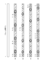
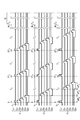
- FIG. 6 is a timing chart showing timings of control pulses G 1 to G 4 in each subframe period F 1 to F 3 set by the charge transfer control means 32 of FIG. 1.
- FIG. FIG. 6 is a timing chart showing timings of control pulses G 1 to G 4 in each subframe period F 1 to F 3 set by the charge transfer control means 32 of FIG. 1.
- FIG. It is a timing chart for demonstrating the principle of distance calculation by the distance image sensor 10 of FIG.
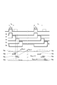
- 5 is a timing chart of various signals handled by the distance image sensor 10 of FIG. 1, and a graph showing changes of various values calculated by the distance image sensor 10 with respect to the delay time T D.
- 5 is a timing chart of various signals handled in another calculation procedure by the distance image sensor 10 of FIG. 1 and a graph showing changes with respect to delay times T D of various values calculated in another calculation procedure by the distance image sensor 10 .
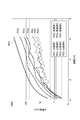
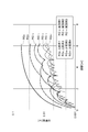
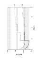
- It is a graph which shows the simulation result of the distance resolution of this embodiment at the time of distance measurement of the distance range of 0.2-6 m.
- FIG. 16 is a timing chart showing control timings of the pulsed light L P and the first to fourth control pulses G 1 to G 4 in the subframe period F 1 in the modification example.
- 16 is a timing chart showing control timings of the pulsed light L P and the first to fourth control pulses G 1 to G 4 in the subframe period F 1 in the modification example. It is a graph which shows the simulation result of the number of electrons generated at the time of signal read-out in the modification at the time of measuring distance in the 0.2-6 m distance range. It is a graph which shows the simulation result of the distance resolution in the modification at the time of measuring distance in the 0.2-6 m distance range.
- In the modification is a timing chart showing generation timing of the application timing and the pulse light L P of the control pulse G 1 ⁇ G 4 by the arithmetic circuit 12. It is an equivalent circuit schematic of the principal part of the pixel circuit 13 in a modification.
- a distance image sensor 10 shown in FIG. 1 is a device that generates a distance image including distance information for each pixel using a time of flight method, and includes a light source 11, an arithmetic circuit 12, and a plurality of pixel circuits (pixel circuit units And 13.).
- the light source 11 includes, for example, a semiconductor light emitting element such as a light emitting diode or a laser diode and a drive circuit for driving the semiconductor light emitting element.
- a semiconductor light emitting element such as a light emitting diode or a laser diode
- a drive circuit for driving the semiconductor light emitting element As the light source 11, an element that generates light in a wavelength region such as a near infrared region or a visible light region can be used.
- the distance image sensor 10 includes a plurality of pixel circuits 13. A plurality of pixel circuits 13, a two-dimensional direction (for example, column and row directions) incident pulses are arranged in a two-dimensional array to constitute an image sensor, pulse light L P has occurred is reflected by the object S The detection signal is generated by photoelectrically converting the light L R.
- the distance image sensor 10 also includes an arithmetic circuit 12.
- the arithmetic circuit 12 calculates distance information on the object S for each pixel using detection signals generated by the plurality of pixel circuits 13, and a distance image including two-dimensional image information on which the distance information for each pixel is reflected. Generate and output.
- the arithmetic circuit 12 may be configured by a dedicated integrated circuit such as a one-chip microcomputer including a CPU, a RAM, a ROM, an input / output device, etc., or may be configured by a general purpose computer such as a personal computer.
- the pixel circuit 13 is formed of a semiconductor element, and has a photoelectric conversion region 21 having a function of converting incident pulse light L R into electric charge, and first to the fourth provided close to the photoelectric conversion region 21 and separated from each other.
- a photoelectric conversion region 21 having a function of converting incident pulse light L R into electric charge
- first to the fourth provided close to the photoelectric conversion region 21 and separated from each other.
- First to fourth control electrodes 24 1 to 24 4 and fifth control electrode 25 for applying control pulses for charge transfer to and from the respective regions, and first to fourth charge readout regions
- voltage detection means 26 1 to 26 4 for reading out the detection signal from each of 22 1 to 22 4 .
- the voltage detection means 26 1 to 26 4 are, for example, amplifiers including a source follower amplifier, and under control of the arithmetic circuit 12, voltages based on the reference potentials of the respective charge readout regions 22 1 to 22 4 selectively Are detected and amplified, and the amplified voltage is output to the arithmetic circuit 12 as first to fourth detection signals.
- the pixel circuit 13 is formed on, for example, a p-type semiconductor substrate such as a silicon substrate. That is, the photoelectric conversion region 21 is a pixel formed of an active region formation layer made of a p-type semiconductor, an n-type surface buried region, a p-type pinning layer, and an insulating film formed in order on a p-type semiconductor substrate. It is provided at the center of the formation area. Then, n-type charge read-out regions 22 1 to 22 4 and charge discharge region 23 having a higher impurity concentration than the n-type surface embedded region are formed at positions separated from each other so as to approach photoelectric conversion region 21.
- Control electrodes 24 1 to 24 4 and 25 are provided on the charge transfer paths from the photoelectric conversion region 21 on the film to the charge reading regions 22 1 to 22 4 and the charge discharging region 23, respectively.
- each of the control electrodes 24 1 to 24 4 and 25 may be provided on the charge transfer path, or may be separately provided to a plurality of electrode portions so as to sandwich the charge transfer path from both sides. .
- control pulses having different phases are applied to the control electrodes 24 1 to 24 4 and 25 from the arithmetic circuit 12 described later.
- a potential gradient is sequentially formed such that charges are transported to any of the charge transfer paths, and the surface embedded region of the photoelectric conversion region 21 is formed.
- the generated majority carriers (charges) are moved to either of the charge readout regions 22 1 to 22 4 and the charge discharging region 23.
- the charge discharging region 23 is a region for discharging the charge generated in the photoelectric conversion region 21.
- the arithmetic circuit 12 includes, as functional components, a light source control unit 31, a charge transfer control unit 32, a distance data validity determination signal generation unit 33, a distance data validity determination unit 34, an invalid pixel identification value generation unit 35, and a distance.
- a calculation reference signal generation unit 36, a distance calculation reference signal selection unit 37, and a distance image generation unit 38 are included.
- Distance data validity determination signal generation means 33, distance data validity determination means 34, invalid pixel identification value generation means 35, distance calculation reference signal generation means 36, distance calculation reference signal selection means 37, and distance image generation means 38 The distance calculating means of the present embodiment is configured.
- Light source control means 31 of the arithmetic circuit 12 emission timing of the pulsed light L P by the light source 11 to control the intensity of the pulse light L P, and the pulse width of the pulse light L P.
- the charge transfer control means 32 of the arithmetic circuit 12 has a function of applying the first to fourth control pulses G 1 to G 4 and the fifth control pulse G D to the control electrodes 24 1 to 24 4 and 25 respectively.
- the charge transfer control means 32 corresponding to each of the generation timing of the pulsed light L P in a sub-frame period, only the control electrodes 24 1 to 24 4 for the duration T 1 is the duration T 0 or more First to fourth control pulses G 1 to G 4 are sequentially applied.
- the duration T 1 is set to be equal to the duration T 0.
- the charge transfer control unit 32 in a period except for the first to third application timing of the control pulse G 1 to G 3 in the sub-frame period, the charges accumulated in the photoelectric conversion region 21 to the charge discharging region 23 a control pulse G D for discharging is applied to the control electrode 25.
- the resolution 15cm distance calculation using the time of flight of the pulse light L P corresponds to the flight time 1 ns
- the control means having a time accuracy of ps order as a guide in order below this resolution is required. Therefore, the charge transfer control unit 32 and the light source control unit 31 need to be designed in consideration of the wiring capacitance integrated with the pixel circuit 13 and the like, and therefore, can be formed on the semiconductor integrated with the pixel circuit 13 desirable.
- "on an integral semiconductor” also includes on different semiconductors among a plurality of semiconductor layers stacked using SOI (Silicon On Insulator) technology or TSV (Through Silicon Via) technology.
- a circuit between the charge transfer control means 32, the circuit between the charge transfer control means 32 and the control electrodes 24 1 to 24 4 , 25 and a circuit between the charge transfer control means 32 and the light source control means 31 The part may be formed on the same semiconductor as the pixel circuit 13 or on a semiconductor layer stacked with the pixel circuit 13.
- one frame period (T f ) which is a repetition period of the distance calculation by the arithmetic circuit 12 is, as shown in FIG. 2, control pulses G 1 to G 4 and G D for respective generation timings of the pulsed light L P. 4 includes four subframe periods F 1 to F 4 having different timings, and a reading period R which is a period during which the first to fourth detection signals are read out among those periods.
- one frame period (T f ) as shown in part (a) of FIG. 2, four subframe periods F 1 to F 4 of different length periods may be cyclically repeated.
- part (c) and part (d) of part 2 four subframe periods F 1 to F 4 of different periods are repeated in an arbitrary order set in advance. It is also good.
- the charge transfer control means 32 of the arithmetic circuit 12 shifts the delay times of the control pulses G 1 to G 4 with respect to the generation timing of the pulsed light L P to different times every four types of subframe periods F 1 to F 4. Timings of the control pulses G 1 to G 4 are set.
- FIG. 3 is a timing chart showing an example of timings of control pulses G 1 to G 4 in each of the subframe periods F 1 to F 3 set by the charge transfer control means 32. Although FIG. 3 shows a timing chart for subframe periods F 1 to F 3 , the subframe period F 4 also has a delay time of control pulses G 1 to G 4 in subframe period F 3 . Set to shift.
- the sub-frame period F 1 is set timing of the control pulse G 1 to match the generation timing of the pulsed light L P to be periodically repeated at time T C, time from one another immediately afterwards
- the timings of the control pulses G 2 to G 4 are set successively so as not to be superimposed on each other, and the control pulse G D is set to be applied in a period other than the application period of the control pulses G 1 to G 4 .
- Readout period R is set immediately after the subframe period F 1.
- pulse light L P control pulse G 1 ⁇ G respective delay time of 4 for the generation timing (hereinafter, this delay time).
- the timings of the control pulses G 1 to G 4 are set such that “range shift” shifts at + 4T 0 .
- the shift width is not limited to the + 4T 0, it may be another shift width such as + 3T 0.
- control such that the respective delay time of the control pulse G 1 ⁇ G 4 for generating timing of the pulse light L P is shifted in the + 4T 0
- the timings of the pulses G 1 to G 4 are set.
- FIG. 4 is a timing chart showing another example of the timing of the control pulses G 1 to G 4 in each of the subframe periods F 1 to F 3 set by the charge transfer control means 32.
- the sub-frame period F 2 as compared to the sub-frame period F 1, such that each delay time of the control pulse G 1 ⁇ G 4 for generating timing of the pulse light L P is shifted in the + 2T 0
- the timings of control pulses G 1 to G 4 are set.
- control such that the respective delay time of the control pulse G 1 ⁇ G 4 for generating timing of the pulse light L P is shifted in the + 2T 0
- the timings of the pulses G 1 to G 4 are set, and the relationship between the subframe period F 4 and the subframe period F 3 is similarly set.
- each sub-frame period F 1 ⁇ F the length of every four set by the arithmetic circuit 12, the repeat count N 1 of the pulse light L P in each sub-frame period F within 1 ⁇ F 4, N 2, N 3 and N 4 (N 1 to N 4 are integers)
- N 1 to N 4 are integers
- Lengths N 1 ⁇ T c , N 2 ⁇ T c , N 3 ⁇ T c , N 4 ⁇ T c , and the generation timing of the pulsed light L P Are set to be longer as the delay time of each of the control pulses G 1 to G 4 with respect to L becomes longer.
- the arithmetic circuit 12 number of repetitions N 1, N 2, N 3 , N 4 of the pulsed light L P in each sub-frame period F within 1 ⁇ F 4, the control pulses for generating timing of the pulse light L P
- Nexp is a predetermined constant.
- the number of acquisitions between subframe periods F 1 to F 4 is weighted so as to increase as the range shift becomes larger.
- the distance calculation means of the arithmetic circuit 12 repeatedly executes the calculation of the distance for each pixel circuit 13 every one frame period, and repeatedly generates a distance image including the resulting distance information.
- the distance calculation means sets the reading period R at every timing of the reading period R shown in part (a) of FIG. 2 (that is, according to the end timing of each subframe period F 1 to F 4 ).
- the following distance calculation is repeatedly performed on the first to fourth detection signals S 1 to S 4 read out, and the average value of the effective distance calculation results obtained as a result is obtained as distance information within one frame period. I assume.
- the distance calculation means calculates four types within one frame period.
- the values of the first to fourth detection signals S 1 to S 4 are summed up in each of the sub-frame periods F 1 to F 4 of each frame, and the summed first to fourth detection signals S 1 to S 4 are targeted
- the calculation of the distance may be executed, and the result of the effective distance calculation among the results may be integrated (averaged etc.) as distance information.
- the distance data validity determination signal generation means 33 constituting the distance calculation means is based on the first to fourth detection signals S 1 to S 4 outputted from the pixel circuit 13 corresponding to the light emission timing of the pulsed light L P.
- the total value of the signal components of the charges generated from the incident pulse light L R excluding the signal component of the background light among the first to fourth detection signals S 1 to S 4 is the distance data validity determination signal S.
- the distance data validity determination signal S A is a signal indicating whether the first to fourth detection signals S 1 to S 4 strongly reflect the incident pulse light L R
- the first to fourth It is a signal for determining whether the calculation of the distance based on the detection signals S 1 to S 4 is valid.
- Distance data validity determining unit 34 determines whether the first to fourth detection signals S 1 to S 4 the calculation of the distance based on valid. Specifically, the distance data validity determining unit 34, the distance data validity determination signal S A with a predetermined threshold value Th 1, when the distance data validity determination signal S A is greater than the threshold value Th 1 is determines the distance calculation to be valid, it is determined that if the distance data validity determination signal S a is the threshold value Th 1 or less is ineffective distance calculation.
- the invalid pixel identification value generation unit 35 generates an identification value indicating whether the distance calculation is invalid for each pixel corresponding to the pixel circuit 13 based on the determination result of the distance data validity determination unit 34.
- Distance calculation reference signal generating means 36 of the distance calculation means based on the first to fourth detection signals S 1 to S 4 which are outputted from the pixel circuit 13 corresponding to the light emission timing of the pulsed light L P, Generate a distance calculation reference signal on which to calculate the distance. Specifically, the distance calculation reference signal generation means 36 sets the value S 1-3 of the difference between the pair S 1 and S 3 of one of the first to fourth detection signals S 1 to S 4 .
- a first distance calculation reference signal X R is generated by calculating the ratio of the difference to the distance data validity determination signal S A.
- the distance calculation reference signal generation means 36 calculates the difference between the value S2-4 of the difference between the set S 2 and S 4 of the other of the first to fourth detection signals S 1 to S 4 and A second distance calculation reference signal Y R is generated by calculating the ratio to the distance data validity determination signal S A.
- the distance calculation reference signal selection means 37 of the distance calculation means determines whether or not the position of the object S can be measured based on the first and second distance calculation reference signals X R and Y R , If it is within the measurable range, either of the first and second distance calculation reference signals X R and Y R is output to the distance image generating means 38 as a valid value. For example, the distance calculation reference signal selection unit 37 determines whether the value of the distance calculation reference signal X R is “0” or more and the value of the distance calculation reference signal Y R is Th 3 or less. It is determined whether the distance calculation reference signals X R and Y R are valid or invalid.
- the distance calculation reference signal selection means 37 selects one of the first and second distance calculation reference signals X R and Y R according to the comparison result of the first distance calculation reference signal X R and the threshold value Th 2 . Is selected, and the selected first and second distance calculation reference signals X R and Y R are output to the distance image generation means 38 as valid values.
- any of the distance calculation reference signals X selected by the distance calculation reference signal selection means 37 for each pixel circuit 13 is selected.
- the distance is calculated for each of the subframe periods F 1 to F 4 with reference to R 1 and Y R, and distance information is calculated from the average of them.
- the distance image generation unit 38 generates a distance image including distance information corresponding to each pixel circuit 13 and outputs the distance image to an external device.
- the external device of the output destination include output devices such as a display device and a communication interface device.
- distance image generation unit 38 the distance for all of the sub-frame periods F 1 ⁇ every subframe period or pixel identification value is generated indicating that the distance calculation is disabled for F 4 F 1 ⁇ F 4
- An invalid value can be embedded in the distance image for pixels determined to have the calculation reference signals X R and Y R outside the measurable range.
- FIG. 5 is a timing chart for explaining the principle of distance calculation by the distance image sensor 10.
- the distance charge in each area of the timing and the pixel circuits 13 of the various signals is controlled by the image sensor 10 indicates the timing accumulated, in order from the top, the light emitting timing of the pulse light L P, the first to fourth control pulses G 1 to G 4 and application timing of the control pulse G D, it shows the charge accumulation timings in the first to fourth charge read area 22 1 to 22 4.
- the first to fourth control pulses G 1 to G 4 are continuously applied for the duration T 0 so as not to overlap each other. There is.
- a ratio of incident pulsed light L R is the electric charge accumulated in the photoelectric conversion region 21 by being photoelectrically converted, corresponding to the delay time T D with respect to pulse light L P of the incident pulse light L R, two charge read area 22 2, 22 3, or the two charge read area 22 3, is distributed to 22 4.
- the light emission timing of the duration T 0 of the pulse light L P by setting the relationship between the first application timing of the control pulse G 1, the charge readout area 22 1 is defined by the control pulse G 1 only the charges of the charge amount N B due to noise such as background light and dark current in the time window is transported.
- the time delay to the charge amount N B is the charge readout area 22 2 while the charge amount of charge N sm1 distributed in response to T D has been added is transported, the charge readout area 22 3, the amount of charge distributed to correspond to the time delay to the charge amount N B T D The charge to which N sm2 has been added is transported.
- G 4 is the charge readout area 22 3 delay to the charge amount N B time T while the charge amount of charge N sm1 distributed in response to D has been added is transported, the charge readout area 22 4, the charge amount N B to the delay distributed corresponds to the time T D charge amount N The charge to which sm2 is added is transported.
- the arithmetic circuit 12 of the range image sensor 10 in accordance with each emission timing of the pulsed light L P, and the charge amount N sm1 excluding the amount of charge N B the amount of charge N B
- the distance to the object S corresponding to the delay time T D can be calculated by calculating the ratio to the removed charge amount N sm2 .
- FIG. 6 is a timing chart of various signals handled by the distance image sensor 10, and a graph showing changes of the calculated various values with respect to the delay time T D.
- the (a) to part (e) portions indicate the timing of the control pulse G 1 ⁇ G 4 and the pulse light L P to (f) section ⁇ (n) portion, respectively, the first to fourth detection signals S 1 to the value of S 4, the difference value S 1-3, the value of S 2-4, the value of the distance data validity determination signal S a, and the distance calculated reference signal X R, Y R
- the (o) portion shows the data effective range at the delay time T D
- the (p) portion shows the measurable range at the delay time T D.
- FIG. 6 shows various signals and values handled in distance calculation for subframe period F 1
- delay time T for distance calculation for subframe periods F 2 to F 4 is also shown in FIG. The same is true except that D shifts.
- the light source control means 31 and the charge transfer control means 32 of the arithmetic circuit 12 make a period of one frame constituted by subframe periods F 1 to F 4 timing of the control pulse G 1 ⁇ G 4 and the pulse light L P is controlled by the inner (light source control step, the charge transfer control step).
- the first to fourth detection signals S 1 to S 4 are read out by the voltage detection means 26 1 to 26 4 of each pixel circuit 13, and those detection signals S 1 to S 4 are It is output to the arithmetic circuit 12 (voltage detection step).
- the distance data validity determination unit 34 compares the value of the distance data validity determination signal S A with the threshold value Th 1 to determine whether the calculation of the distance using the detection signals S 1 to S 4 is valid. Determine if For example, by setting the threshold value Th 1 in the vicinity of “0”, as shown in part (o) of FIG. 6, the value between “ ⁇ 1” and “0” of the delay time T D is “3” to It is determined that the range up to a value between "4" is the "data effective range" in which the distance calculation is effective.
- the distance calculation reference signal selection means 37 determines whether the value of the distance calculation reference signal X R is within a predetermined range, whereby the value to be referred to for the distance calculation is the distance calculation reference signal X. It is selected from among R and a distance calculation reference signal Y R. For example, when the value of the distance calculation reference signal X R is “0” or more and the threshold value Th 2 or less, the distance calculation reference signal X R is selected, and when the value of the distance calculation reference signal X R exceeds the threshold value Th 2 A distance calculation reference signal Y R is selected. By such determination, it is possible to select a distance calculation reference signal in which a detection signal of a time window in which the incident timings of the incident pulse light L R overlap according to the position of the object S.
- the distance calculation reference signal selection means 37 determines whether the value of the selected distance calculation reference signals X R and Y R is within a predetermined range, whereby the object S is within the measurable range. Is determined. For example, it is determined whether the value of the distance calculation reference signal X R is “0” or more, and it is determined whether the value of the distance calculation reference signal Y R is less than or equal to the threshold value Th 3 .
- the distance calculation reference signal X R selected with respect to the corresponding pixel
- the distance of the object S is calculated based on Y R
- the calculation result of each subframe period F 1 to F 4 is averaged to calculate distance information, and a distance image including the calculated distance information of each pixel is generated and It is output.
- the distance calculation by the distance image sensor 10 described above may be performed according to the following other procedure (hereinafter, also referred to as “4-tap 4-zone 4-subframe scheme”). According to this procedure, the “data effective range” and the “measurable range” in the delay time T D can be expanded.
- FIG. 7 is a timing chart of various signals handled in another calculation procedure by the distance image sensor 10, and a graph showing a change with respect to delay time T D of various values calculated in another calculation procedure.
- the (a) to part (e) portions indicate the timing of the control pulse G 1 ⁇ G 4 and the pulse light L P to (f) section ⁇ (o) portion, respectively, the first to fourth detection signals S 1 to the value of S 4, the difference value S 1-3, the value of S 2-4, the distance data validity determination signal value of S a, and the distance calculated reference signal R 1, R 2 , R 3 corresponding to the delay time T D , (p) indicates the data effective range at the delay time T D , and (q) indicates the data effective range corresponding to the delay time T D
- the calculated values of the comparison signals P 2 to P 4 and the (r) part indicate the measurable range in the delay time T D.
- FIG. 7 shows various signals and values handled in distance calculation for subframe period F 1
- delay time T is also calculated for distance calculation for subframe periods F 2 to F 4. The same is true except that D shifts.
- the light source control means 31 and the charge transfer control means 32 of the arithmetic circuit 12 make a period of one frame constituted by subframe periods F 1 to F 4 .
- timing of the control pulse G 1 ⁇ G 4 and the pulse light L P is controlled by the inner (light source control step, the charge transfer control step).
- the control pulse G D is set to be applied in a period other than the application period of the control pulse G 1 ⁇ G 4.
- the control pulse G 3 is turned on, immediately after the four control pulses G 1 ⁇ G 4 are on continuously, the control pulse G 1 is turned on again Ru.
- the first to fourth detection signals S 1 to S 4 are read out by the voltage detection means 26 1 to 26 4 of each pixel circuit 13, and those detection signals S 1 to S 4 are It is output to the arithmetic circuit 12 (voltage detection step).
- distance information for each pixel in units of subframe periods F 1 to F 4 is calculated by the arithmetic circuit 12 (distance calculation step ). That is, the distance data validity determination signal generating means 33, a difference value S 2-4 of the detection signal S 1, a difference value S 3 S 1-3 and the detection signal S 2, S 4 is calculated. In addition, the distance data validity determination signal generating means 33, based on the absolute value of the difference value S 1-3 and the difference value S 2-4, the value of the distance data validity determination signal S A is calculated.
- the distance data validity determination unit 34 compares the value of the distance data validity determination signal S A with the threshold value Th 1 to determine whether the calculation of the distance using the detection signals S 1 to S 4 is valid. Determine if For example, by setting the threshold value Th 1 in the vicinity of “0”, as shown in part (p) of FIG. 7, the value between “ ⁇ 1” and “0” of the delay time T D is “4” to It is determined that the range to a value between "5" is the "data effective range" in which the distance calculation is effective.
- the value of the distance calculated reference signal R 3 using is calculated.
- a value to be referred to for distance calculation is one of the distance calculation reference signals R 1 to R 3 . It is selected from For example, distance calculation reference signal R 1 is the threshold Th 2 or less, and, when the distance calculated reference signal R 2 is the threshold value Th 5 below, the distance calculation reference signal R 1 is selected. On the other hand, the distance is calculated reference signal R 1 exceeds the threshold value Th 2, and, when the distance calculated reference signal R 2 is the threshold value Th 5 below, the distance calculation reference signal R 2 is selected. Furthermore, when the distance calculated reference signal R 2 exceeds the threshold Th 5 is distance calculation reference signal R 3 is selected. By such determination, it is possible to select a distance calculation reference signal in which a detection signal of a time window in which the incident timings of the incident pulse light L R overlap according to the position of the object S.
- the distance calculation reference signal selection means 37 determines whether the value of the selected distance calculation reference signals R 1 and R 3 is within a predetermined range, whereby the object S is in a measurable range. Is determined. For example, the distance value of the calculation reference signal R 1 is judged whether it is more "0", the value of the distance calculated reference signal R 3 is whether the threshold Th 6 or less is determined.
- the distance calculation reference signal R 1 ⁇ selected for the corresponding pixel
- the distance of the object S is calculated based on R 3
- the calculation result of each subframe period F 1 to F 4 is averaged to calculate distance information, and a distance image including the calculated distance information of each pixel is generated and It is output.
- the calculable range of the delay time T D can be expanded, and the time width of the time window can also be reduced.
- the distance calculation is performed by selecting a value that changes linearly with respect to the delay time T D among the distance calculation reference signals R 1 , R 2 and R 3 , corresponding to the range in which the object S is located
- An appropriate distance data reference signal value can be used to calculate the distance, and an accurate image signal can be generated regardless of the position of the object S.
- pulse light L P is generated from the light source 11 in four sub-frame periods F within 1 ⁇ F 4 contained in one frame period, pulse light L P Corresponding to the generation of the pulse light LP, the time window of the duration T 1 of the duration T 0 or more of the pulse light L P is sequentially set, and the first to fourth charges from the photoelectric conversion region 21 of the pixel circuit 13 in that time window The charges are sequentially transferred to the reading areas 22 1 to 22 4 , and the charges are discharged from the photoelectric conversion area 21 to the charge discharging area 23 in the period other than the time window.
- the first to fourth detection signals S 1 to S 4 are read out from the first to fourth charge readout regions 22 1 to 224 of the pixel circuit 13 every subframe period F 1 to F 4 , and those The distance is calculated repeatedly based on At this time, the delay time (range shift) of the time window with respect to the generation timing of the pulsed light L P is set to shift to different time every four types of sub-frame periods F 1 to F 4 .
- time windows of eight types of range shifts are set.
- the distance calculation means of the arithmetic circuit 12 calculates the distance for each of the subframe periods F 1 to F 4 . In this case, it is possible to calculate a distance with high distance resolution according to the distance measurement range of the object S.
- the distance in the image sensor 10 the number of repetitions of the pulse light L P in each of the sub-frame periods F 1 ⁇ F 4 within one frame period, are weighted to be larger as the shift time of the range shift is longer There is.
- the number of times the light pulse is projected (the number of times the charge is accumulated in the pixel) is increased for frames in the far distance measurement range according to the distance measurement range in each subframe period F 1 to F 4.
- the number of times of light emission (the number of times of charge accumulation in a pixel) can be reduced for a frame in a distance range, and distance resolution can be improved.
- the subframe periods F 1 to F 4 are weighted by the square of the distance measurement distance.
- the minimum value of the distance resolution is improved by 2 1/2 times as compared to the case where the number of times of light emission is allocated evenly between subframe periods.
- each of the sub-frames generated in response to the application of the first to fourth control pulses G 1 to G 4 in each of the sub-frame periods F 1 to F 4 of the weighted and set period The voltages of the first to fourth charge readout regions 22 1 to 22 4 are read out as first to fourth detection signals S 1 to S 4 , and the distance calculation is performed using them.
- the saturation of the detection signals S 1 to S 4 caused by the strong background light can be prevented, the dynamic range of distance measurement can be improved.
- FIGS. 8 and 9 show simulation results of the distance resolution of the present embodiment when the distance range of 0.2 to 6 m is measured in comparison with the comparative example.
- FIG. 8 shows the resolution in the measurement under background light of 100 klux
- FIG. 9 shows the resolution in the measurement under background light of 0 lux.
- Comparative Example 1 when one type of range shift is set for each subframe and one type of subframe is set in one frame period, in Comparative Example 2, two types of range shift are set for each subframe, When one type of subframe is used in one frame period, in Comparative Example 3, three types of range shifts are set for each subframe, and when one type of subframe is used in one frame period, Comparative Example 4 is used.
- the first embodiment sets four types of range shifts for each subframe, and shifts the range shift of a subframe to two types in two subframe periods in one frame period.
- the third embodiment has four types of shift for each subframe.
- the case of setting the range shift and shifting the range shift of the sub-frame to four types in four sub-frame periods within one frame period is shown.
- the resolution of approximately 7 m is estimated in the distance measurement of 6 m in Comparative Example 1, while in Examples 1 to 3, the resolution improves as the number of subframe periods increases. In Example 3, it turned out that it improves to resolution of 20 cm by distance measurement of 6 m. Further, as shown in FIG. 9, while the resolution of about 5.5 cm is estimated in the distance measurement of 6 m in Comparative Example 1, the number of subframe periods is increased in Examples 1 to 3. It has been found that the resolution is improved according to and in Example 3 it is improved to a resolution of 8 mm with a distance measurement of 6 m.
- the simulation result of the distance resolution of the present embodiment when the distance range of 0.2 to 6 m is measured under a background light of 100 klux is weighted in the case of weighting the subframe period length. It shows by comparing with the case where it does not.
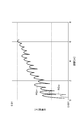
- FIG. 11 shows a simulation result of the number of generated electrons for each signal readout in the present embodiment when the distance range of 0.2 to 6 m is measured under background light of 100 klux in comparison with the comparative example.
- the graph CG 1 shows the number of electrons generated when reading out a signal in units of one frame period in Comparative Example 4, and the graph CG 2 is set as shown in part (d) of FIG. 2 in Example 3.
- the figure shows the number of electrons generated when reading out a signal in units of subframe periods F 1 to F 4 .
- the number of generated electrons in signal readout is suppressed in a wide measurement range.
- the present embodiment by performing signal readout for each sub-frame, it is possible to prevent saturation due to a large amount of charge due to strong background light such as sunlight.
- the number of saturated electrons in the charge detection unit of the pixel can be set relatively low, the size of the capacitor incorporated in the pixel for charge detection can be reduced. For example, if the number of electrons can be reduced to 100,000 or less, it is possible to cope with 100 klux of background light with a 10 fF capacitor. Since the capacitor can be made smaller, the conversion gain can be increased, which is also advantageous for noise.
- the four charge readout areas 22 1 to 22 4 are provided in the pixel circuit 13, but any number of charge readout areas may be provided as long as it is three or more.
- the control electrode and the voltage detection means are provided corresponding to the number of charge readout regions, and the arithmetic circuit 12 calculates distance information based on the detection signals read out from the respective charge readout regions.
- any two or more subframe periods may include subframe periods of any kind.
- the charge transfer control means 32 of the arithmetic circuit 12 to the generation timing of the pulsed light L P, depending on the number of types of sub-frame periods, so that the delay time of the control pulse is shifted at different times Set the timing of control pulse.
- the distance calculation means of the arithmetic circuit 12 is configured to calculate the distances for the first to fourth detection signals S 1 to S 4 every four types of subframe periods F 1 to F 4 within one frame period. The calculation was running. However, it is not limited to such an aspect.
- the distance calculation means may perform distance calculation for detection signals detected across two subframe periods F 1 and F 2 .
- the detail of the procedure of the distance calculation by the distance calculation means of the arithmetic circuit 12 in the modification of such an aspect will be described with reference to FIG.
- the calculation of the distance is performed based on the detection signal detected across two subframe periods F 1 and F 2 , but similarly, two subframe periods F 2 and F
- the calculation of the distance may be performed based on the detection signal detected across three or two subframe periods F 3 and F 4 .
- FIG. 12 is a timing chart of various signals handled by the present modification, and a graph showing changes of calculated various values with respect to delay time T D. 12, is applied to the (a) portion ⁇ (c) portion, respectively, the sub-frame control pulse is applied in the period F 1 G 1 (1) ⁇ G 4 (1), in the sub-frame period F 2
- the timings of the control pulses G 1 (2) to G 4 (2) and the pulsed light L P are shown, and are detected in sub-frame periods F 1 and F 2 in parts (d) to (e), respectively.
- the values of the first to fourth detection signals S 1 (1) to S 4 (1) and S 1 (2) to S 4 (2) are shown. Further, in FIG.
- the difference values S 1-3 (1) , S 1-3 (2) , S 2-4 (1) , S 2-4 (2 ) value of) (in h) section ⁇ (i) section, the distance data validity determination signal S a (1), the value of S a (2), the portion (j) section ⁇ (o) is the distance calculated
- the values of reference signals X R (1) , Y R (1) , X R (B) , Y R (B) , X R (2) , Y R (2) are shown corresponding to delay time T D.
- the (p) part shows the data effective range at the delay time T D
- the (q) part shows the measurable range at the delay time T D.
- the arithmetic circuit 12 is the same as the above embodiment in that the detection signals S 1 (1) to S 4 (1) , S 1 ( detected in the respective subframe periods F 1 and F 2 ) . based on 2) ⁇ S 4 (2) , the difference value S 1-3 (1), S 1-3 (2), S 2-4 (1), to calculate the S 2-4 (2). Then, based on these difference values, the arithmetic circuit 12 performs the distance data validity determination signals S A (1) , S A corresponding to the subframe periods F 1 and F 2 in the same manner as in the above-described embodiment. Calculate the value of (2) .
- the values of the respective distance data validity determination signals S A (1) and S A (2) are compared with the threshold value Th 1 to detect the respective detection signals S 1 (1) to S 4 (1) , It is determined whether the calculation of the distance using S 1 (2) to S 4 (2) is valid. For example, by setting the threshold value Th 1 in the vicinity of “0”, as shown in part (p) of FIG. 12, the value between “ ⁇ 1” and “0” of the delay time T D is “7” to It is determined that the range to a value between "8" is the "data effective range” in which the calculation of the distance is effective.
- the distance calculation reference signal X R is calculated using the following equations (10) and (11) based on the detection signals detected across the two subframe periods F 1 and F 2. (B) , Y R (B) values are calculated.
- the value referred to for the distance calculation by the arithmetic circuit 12 is the distance calculation reference signal X R (1) , X R (B) , X R (2) and the distance calculation reference signal Y R (1) , Y R (B) , Y R (2) are selected.
- the distance calculation reference signals X R (1) and Y R (1) are obtained in the same manner as the above embodiment.
- one of the distance calculation reference signals X R (1) and Y R (1) is selected.
- the values of the distance calculation reference signals X R (2) and Y R (2) are calculated in the same manner as the above embodiment. In response, one of the distance calculation reference signals X R (2) and Y R (2) is selected.
- the distance calculation reference signals X R (1) and X R (2 ) and distance calculation reference signal Y R (1) when not selected any of the values from among the Y R (2), the distance calculated reference signal X R (B), Y values of R (B) Depending on, either of the distance calculation reference signals X R (B) and Y R (B) is selected.
- the distance calculation reference signal selected for the corresponding pixel Based on X R (1) , X R (B) , X R (2) , Y R (1) , Y R (B) , Y R (2) , the distance of the object S is calculated.
- the calculation results in the frame periods F 1 to F 4 are averaged to calculate distance information, and a distance image including the calculated distance information of each pixel is generated and output.
- an accurate image signal can be generated regardless of the position of the object S. For example, if four time windows are set for each sub-frame period and the distance is calculated for every three sub-frame periods, it is simple when the incident pulse light L R is incident to the eleven time windows. The distance can be determined by any calculation. Similarly, when N types of subframe periods in which M time windows are set are set, it is assumed that incident pulse light L R is incident corresponding to continuous M ⁇ N ⁇ 1 time windows. Distance can be calculated.
- control pulse G 1 among the first to fourth control pulses G 1 to G 4 is changed during the four types of subframe periods F 1 to F 4. May be configured.
- the control of the application timing of the control pulses G 1 to G 4 by the charge transfer control means 32 of the arithmetic circuit 12 in the modification of such an embodiment will be described in detail with reference to FIG.
- FIG. 13 is a timing chart showing control timings of the pulsed light L P and the first to fourth control pulses G 1 to G 4 in the subframe period F 1 in the present modification.
- FIG. 13 shows a timing control in the sub-frame period F 1, the timing control in the other sub-frame periods F 2 ⁇ F 4, same as the control state shown in FIG. 3 or FIG. 4 It may be.
- the pulse light L P first to fourth control pulses G 1 to G delay time is short sub-frame periods F 1 to F 4 4 for application timing of sequentially
- the rate of the number of times of application of the first to fourth control pulses G 1 to G 4 (the number of applications per unit time) in the order of the fourth to first control pulses G 4 to G 1
- control the application timing of the first to fourth control pulses G 1 to G 4 it is sufficient that at least a first rate of application times of the control pulse G 1 is lowered. That is, in the example shown in FIG.
- the charge transfer control means 32, in the shortest subframe period F 1 is the delay time, controlled to thin out the number of applications of the control pulse G 1 ⁇ G 3, sub-frame periods F 1
- the number of times of thinning is controlled so as to increase in the order of the third to first control pulses G 3 to G 1 . More specifically, the number of times of application of the first to fourth control pulses G 1 to G 4 in the subframe period F 1 is N 1 ⁇ (1 ⁇ 4), N 1 ⁇ (2/4), respectively. It is controlled to become N1 ⁇ (3/4), N1.
- control timing of the pulse light L P and the first to fourth control pulses G 1 to G 4 in the sub-frame periods F 1 may be controlled as shown in FIG. 14.
- the first to fourth rate of application times of the control pulse G 1 to G 4 in having a delay time corresponding to the distance range to be measured is applied immediately after application of the light L P, the fourth to the first control pulse
- the application timings of the first to fourth control pulses G 1 to G 4 are controlled so as to lower in the order of G 4 to G 1 .
- it is sufficient that at least a first rate of application times of the control pulse G 1 is lowered. That is, in the example shown in FIG.
- the charge transfer control unit 32 measures a part of the control pulses G 1 to G 3 as a measurement target immediately before the application of the pulsed light L P in the subframe period F 1 with the shortest delay time. distance range to control to change the timing of non delay time equivalent, the number of changes applied timing in the sub-frame period F 1, to increase in the third to the first order of control pulses G 3 to G 1 To control. By applying the control pulses G 3 to G 1 whose application timing has been changed as described above, only the background light is reflected on the detection signal.
- the number of times of application of the first to fourth control pulses G 1 to G 4 applied immediately after the application of the pulsed light L P in the subframe period F 1 is N 1 ⁇ (1/1 / 4), N1 ⁇ (2/4), N1 ⁇ (3/4), N1 are controlled.
- the target S in the near distance measurement range when the target S in the near distance measurement range is targeted, saturation of the detection signal can be prevented. As a result, the dynamic range of distance measurement can be improved. That is, when the target S in the short distance region is targeted, the number of generated electrons may be very large due to the strong incident pulse light L R , and the number of saturated electrons in the pixel circuit 13 may be exceeded. In this modification, in the sub-frame period in which the time window for the measurement of the short distance region is set, the number of charges taken in by the time window is reduced to suppress the number of generated electrons.
- the number of generated electrons in the pixel circuit 13 can be contained in the range of the number of saturated electrons, and while the distance resolution in the case of targeting the object S in the long distance region is sufficiently enhanced, The distance resolution in the target case can also be maintained at a sufficient value.
- FIG. 15 shows a simulation result of the number of generated electrons for each signal readout in the present modification when the distance range of 0.2 to 6 m is measured under background light of 0 lux.
- Graph CG 3 is a frame in the case of thinning the first number of applications of the control pulse G 1 of the sub-frame periods F 1 to 1/4, and decimating the second number of applications of the control pulse G 2 of the 2/4 It shows the number of electrons generated in the period.
- a graph CG 4 shows the number of electrons generated in one frame period in the case where no thinning the first to fourth control pulses G 1 to G 4 in. As shown in these results, in the present modification, the number of generated electrons in signal readout is suppressed in a close measurement range up to a distance of about 1 m.
- FIG. 16 shows a simulation result of distance resolution in the present modified example when distance measurement of a distance range of 0.2 to 6 m is performed under 0 lux background light.
- Graph RG 17 the distance resolution in the case of thinning the first number of applications of the control pulse G 1 of the sub-frame periods F 1 to 1/4, and decimating the second number of applications of the control pulse G 2 of the 2/4 Is shown.
- a graph RG 18 shows the distance resolution in a case where no thinning the first to fourth control pulses G 1 to G 4 in. As shown in the graph RG 17, in this modification, the distance resolution even when thinning control pulses is suppressed to less than about 3.2mm at a distance of 0.8 m.
- the length of each subframe period F 1 to F 4 becomes longer as the delay time of each of the control pulses G 1 to G 4 with respect to the generation timing of the pulsed light L P becomes longer. It is set.
- the intensity of the pulsed light L P in each of the sub-frame periods F 1 ⁇ F 4 within one frame period, each of the control pulses G 1 ⁇ G 4 for generating timing of the pulse light L P It may be set to be weighted so as to become weaker as the delay time of.
- Figure 17 is in a modification of this aspect, shows the generation timing of the application timing and the pulse light L P of the control pulse G 1 ⁇ G 4 by the charge transfer control means 32 and the light source control means 31 of the arithmetic circuit 12 There is.
- the light source control means 31 of the arithmetic circuit 12 the intensity of the pulsed light L P generated in each sub-frame period F in 1 ⁇ F 3, respectively, I 1, I 2, I 3 (I 1 ⁇ It is set as I 2 ⁇ I 3 ).
- the weighting is set as shown in FIG.
- the intensity of the pulsed light L P subframe period F 4 is similarly set. At this time, number of repetitions N 1 ⁇ N 4 of the pulsed light L P in each sub-frame period F 1 ⁇ F 4 is equally set.
- the light emission intensity of the light pulse is increased for the frame of the far distance measurement range, and the frame of the near distance measurement range is obtained.
- the light emission intensity can be lowered and the distance resolution can be enhanced.
- the intensity of the incident pulse light L R becomes weak in inverse proportion to the square of the distance
- the intensity of the light pulse is weighted by the square of the distance measurement distance.
- stronger pulsed light can be used for the longest ranging distance subframe period in which the distance resolution is most reduced, and the lowest value of the range resolution (which may occur in the longest ranging distance subframe period) ) Can be improved.
- charge readout is performed as the delay time of control pulses G 1 to G 4 with respect to the generation timing of pulsed light L P becomes shorter in each subframe period F 1 to F 4 in one frame period.
- Control may be performed to increase the capacitance of the regions 22 1 to 22 4 .
- FIG. 18 shows an equivalent circuit diagram of the main part of the pixel circuit 13 in the modification of such a mode.
- the photodiode D ij corresponds to the photoelectric conversion region 21
- the gate terminal of the charge discharging MOS transistor Q D corresponds to the fifth control electrode 25
- the gate terminal of the transfer MOS transistor Q 1T ⁇ Q 4T Respectively correspond to the first to fourth control electrodes 24 1 to 24 4 .
- the electrostatic induction channel portion from the photodiode D ij to the transfer MOS transistors Q 1T to Q 4T is represented by junction type field effect transistors Q P1 and Q P2 whose own gate terminals are grounded.
- the two intermediate taps of the junction field effect transistor Q P1, Q P2 connected in series, is connected a source terminal of the charge discharging MOS transistor Q D, the power drain terminal of the charge discharging MOS transistor Q D is at a high potential Connected to V DD .
- one end of each of the transfer MOS transistors Q 1 T to Q 4 T is represented as a configuration in which the junction field effect transistor Q P2 is connected in a T-shape.
- charge readout regions 22 1 to 22 4 and voltage detection means 26 1 to 26 4 are connected to the other end of each of transfer MOS transistors Q 1T to Q 4T.
- a capacitor Cka for charge storage is connected between node Dk and the ground, and in parallel with it, a capacitance switch MOS transistor Q kb and a capacitor C kb for charge storage are provided. And a series circuit of a capacitance switching MOS transistor Qkc and a charge storage capacitor Ckc . Then, four gate terminals of capacitance switching MOS transistor Q kb are connected to control line SC b, and four gate terminals of capacitance switching MOS transistor Q kc are connected to control line SC c.
- control signals from the control means 32 is supplied to the control line SC b and a control line SC c, MOS transistors Q kb and MOS transistor Q kc on / off capacitive switch capacitor switch is a controllable independently.
- the charge transfer control means 32 can control the capacitances of the charge readout regions 22 1 to 22 4 to change in four ways.
- the node D k is connected to the gate terminal of the amplifying transistor Q kA constituting a source follower circuit for reading a potential change accompanying the change in the charge amount of the node D k, further to node D k, after the signal readout
- the reset transistor Q kR for initializing the signal charge is connected.
- the source terminal of the amplifying transistor Q kA is selected transistor Q kS as a switch for reading pixel selection is connected, the output of the select transistor Q kS is connected to the signal read line S k for reading a detection signal There is.
- the charge transfer control means 32 of the arithmetic circuit 12 when reading a detection signal to transfer the charge in each sub-frame periods F 1 ⁇ F 4, with the charge readout area 22 1 to 22 3
- the capacities are set to C 1 , C 2 , C 3 (C 1 > C 2 > C 3 ), respectively.
- the light source 11 is a point light source
- the weighting is set as shown in FIG.
- C ka: C kb: C kc 1: 3: and 5
- C 1 C ka + C kb + C kc
- C 2 C ka + C kb
- Capacitance of the charge readout area 22 4 is also set similarly. At this time, number of repetitions N 1 ⁇ N 4 of the pulsed light L P in each sub-frame period F 1 ⁇ F 4 is equally set.
- the capacity for storing charge is small for frames in the far distance measurement range, and for frames in the near distance measurement range. Can increase the capacity for storing charge and can improve the distance resolution.
- the intensity of the incident pulse light L R is weakened in inverse proportion to the square of the distance, a smaller capacity can be used for the sub-frame period of the longest ranging distance where the distance resolution is most reduced, The lowest value of distance resolution (which may occur in the longest ranging distance subframe period) can be improved. As a result, it is possible to prevent the reduction of the distance resolution in the distance measurement range where the distance is far, and to maintain the distance resolution efficiently as a whole.
- the distance calculating means may detect the first to Mth detection signals detected in response to the application of the first to Mth control pulses in each of the first to Nth subframe periods.
- the distance may be calculated using In this case, it is possible to calculate a distance with high distance resolution according to the distance measurement range of the object.
- the distance calculating means may detect the first to Mth detections detected in response to the application of the first to Mth control pulses within two subframes of the first to Nth subframes.
- the signal may be used to calculate the distance. In this case, it is possible to calculate an unbroken distance across a plurality of distance measurement ranges of the object.
- the number of repetitions of pulsed light in each of the first to N-th (N is an integer of 2 or more) sub-frame periods in one frame period is the number of control light pulses It may be weighted such that the longer the delay time, the more it becomes. As a result, it is possible to prevent the reduction of the distance resolution in the distance measurement range where the distance is far and to maintain the distance resolution efficiently as a whole.
- the voltage detection means is configured to set the voltages of the first to Mth charge readout regions generated in response to the application of the first to Mth control pulses for each subframe period of the weighted and set period. It may be read out as the first to Mth detection signals. In this case, as a result of being able to prevent the saturation of the detection signal caused by the strong background light, the dynamic range of distance measurement can be improved.
- the charge transfer control means is configured to sequentially apply the first to the second sub-frame periods as the delay time of the first to M-th control pulses with respect to the generation timing of the pulsed light becomes shorter. It may be set to lower the rate of the number of applications of at least the first control pulse of the Mth control pulse. With this configuration, saturation of the detection signal can be prevented when an object in a close distance measurement range is targeted. As a result, the dynamic range of distance measurement can be improved.
- the charge transfer control means may be adapted to sequentially apply the first to the second sub-frame periods as the delay time of the first to M-th control pulses with respect to the generation timing of the pulsed light becomes shorter.
- the number of applications of at least the first control pulse of the Mth control pulse may be set to be reduced.
- the intensity of the pulsed light in each of the first to Nth sub-frame periods in the one frame period has a short delay time of the first to Mth control pulses with respect to the generation timing of the pulsed light. It may be weighted so as to be weak to such an extent. In this case, when an object in a close distance measurement range is targeted, saturation of the detection signal can be prevented. As a result, the dynamic range of distance measurement can be improved.
- the delay time of the first to Mth control pulses with respect to the generation timing of the pulse light becomes shorter, It may be controlled to increase the capacitance of the Mth charge readout region.
- saturation of the detection signal can be prevented.
- the dynamic range of distance measurement can be improved.
- an image sensor in which pixel circuit portions are arranged in a two-dimensional array may be included. According to this configuration, it is possible to generate a distance image including highly accurate two-dimensional distance information regardless of the position of the object.
- One aspect of the present invention is applied to a distance image measuring device and a distance image measuring method for generating a distance image including distance information for each pixel, and distance resolution is improved for objects in various distance measuring ranges.
- Image signal can be generated.
- SYMBOLS 10 Distance image sensor (distance image measuring device) 11, Light source, 12 ... Arithmetic circuit, 13 ... Pixel circuit (pixel circuit part), 21 ... Photoelectric conversion area, 22 1 to 22 4 ... Charge readout area, 23 ... Charge Discharge area, 24 1 to 24 4 , 25 ... control electrode, 26 1 to 26 4 ... voltage detection means, 31 ... light source control means, 32 ... charge transfer control means, 33 ... distance data validity judgment signal generation means, 34 ... distance data validity determination unit, 35 ... invalid pixel identification value generation unit, 36 ... distance calculation reference signal generator, 37 ... distance calculation reference signal selecting means, 38 ... distance image generation unit, F 1 ⁇ F 4 ... subframe period , G 1 to G 4 , G D ... control pulse, L P ... pulse light, S ... object.
Landscapes
- Engineering & Computer Science (AREA)
- Physics & Mathematics (AREA)
- General Physics & Mathematics (AREA)
- Multimedia (AREA)
- Signal Processing (AREA)
- Radar, Positioning & Navigation (AREA)
- Remote Sensing (AREA)
- Computer Networks & Wireless Communication (AREA)
- Electromagnetism (AREA)
- Optical Radar Systems And Details Thereof (AREA)
- Transforming Light Signals Into Electric Signals (AREA)
- Studio Devices (AREA)
Abstract
距離画像センサ10は、パルス光LPを発生させる光源11と、光源11を制御する光源制御手段31と、光電変換領域21、電荷読出領域221~224、電荷排出領域23、及び制御電極241~244,25を有する画素回路13と、制御電極241~244に制御パルスを順次印加する電荷転送制御手段32と、電荷読出領域221~224の電圧を検出信号S1~S4として読み出し、検出信号S1~S4を基に距離を繰り返し計算する距離計算手段とを備え、電荷転送制御手段32は、1フレーム期間内の4種類のサブフレーム期間F1~F4ごとに、パルス光LPの発生タイミングに対する制御パルスの遅れ時間を異なる時間にシフトさせるように制御パルスのタイミングを設定する。
Description
本発明の一側面は、画素毎に距離情報を含む距離画像を生成する距離画像測定装置および距離画像測定方法に関する。
従来から、光の飛行時間を用いて距離情報を含む画像信号を生成するセンサ装置が用いられている(例えば、下記特許文献1参照)。このセンサは、時間軸上に配列された第1~第5フレームにおいて第1~第5のパルスの列を照射パルスとして対象物に照射し、ピクセルアレイにおいて対象物の距離情報を含む画像信号を生成する。このような構成により、距離分解能を低下させることなく距離計測範囲を拡大することができる。
しかしながら、上述した従来のセンサ装置では、様々な距離計測範囲の対象物の距離情報を含む画像信号を生成しようとする場合に、さらに距離分解能を向上させようとするためには改善の余地があった。
本発明の一側面は、上記課題に鑑みて為されたものであり、様々な距離計測範囲の対象物を対象にして距離分解能が向上された画像信号を生成することが可能な距離画像測定装置及び距離画像測定方法を提供することを目的とする。
上記課題を解決するため、本発明の一形態にかかる距離画像測定装置は、パルス光を発生させる光源と、第1の持続時間を有するパルス光を1フレーム期間内に含まれる第1~第N(Nは2以上の整数)のサブフレーム期間内で定期的に繰り返し発生させるように光源を制御する光源制御手段と、光を電荷に変換する光電変換領域、光電変換領域に近接して互いに離間して設けられた第1~第M(Mは2以上の整数)の電荷読出領域、電荷を排出するための電荷排出領域、及び光電変換領域と第1~第Mの電荷読出領域および電荷排出領域とに対応してそれぞれ設けられ、光電変換領域と第1~第Mの電荷読出領域および電荷排出領域との間における電荷転送のための第1~第M+1の制御パルスを印加するための第1~第M+1の制御電極を有する画素回路部と、光源制御手段によるパルス光の発生に対応して、第1の持続時間以上である第2の持続時間の間だけ第1~第Mの制御電極に第1~第Mの制御パルスを順次印加し、第1~第Mの制御パルスの印加期間以外の期間に第M+1の制御電極に第M+1の制御パルスを印加する電荷転送制御手段と、電荷転送制御手段による第1~第Mの制御パルスの印加後に、画素回路部の第1~第Mの電荷読出領域の電圧を第1~第Mの検出信号として読み出す電圧検出手段と、第1~第Mの検出信号を基に距離を繰り返し計算する距離計算手段とを備え、電荷転送制御手段は、1フレーム期間内の第1~第N(Nは2以上の整数)のサブフレーム期間ごとに、パルス光の発生タイミングに対する第1~第Mの制御パルスの遅れ時間を異なる時間にシフトさせるように、第1~第Mの制御パルスのタイミングを設定する。
あるいは、本発明の他の形態にかかる距離画像測定方法は、光源制御手段が、第1の持続時間を有するパルス光を1フレーム期間内に含まれる第1~第N(Nは2以上の整数)のサブフレーム期間内で定期的に繰り返し発生させるように光源を制御する光源制御ステップと、光を電荷に変換する光電変換領域、光電変換領域に近接して互いに離間して設けられた第1~第M(Mは2以上の整数)の電荷読出領域、電荷を排出するための電荷排出領域、及び光電変換領域と第1~第Mの電荷読出領域および電荷排出領域とに対応して設けられた第1~第M+1の制御電極を有する画素回路部を用いて、電荷転送制御手段が、光源制御手段によるパルス光の発生に対応して、第1の持続時間以上である第2の持続時間の間だけ第1~第Mの制御電極に、電荷の転送を制御するための第1~第Mの制御パルスを順次印加し、第1~第Mの制御パルスの印加期間以外の期間に第M+1の制御電極に電荷の排出を制御するための第M+1の制御パルスを印加する電荷転送制御ステップと、電圧検出手段が、電荷転送制御手段による第1~第Mの制御パルスの印加後に、画素回路部の第1~第Mの電荷読出領域の電圧を第1~第Mの検出信号として読み出す電圧検出ステップと、距離計算手段が、第1~第Mの検出信号を基に距離を繰り返し計算する距離計算ステップとを備え、電荷転送制御ステップでは、1フレーム期間内の第1~第N(Nは2以上の整数)のサブフレーム期間ごとに、パルス光の発生タイミングに対する第1~第Mの制御パルスの遅れ時間を異なる時間にシフトさせるように、第1~第Mの制御パルスのタイミングを設定する。
上記形態の距離画像測定装置あるいは距離画像測定方法によれば、1フレーム期間内に含まれる2つ以上のサブフレーム期間内で光源から定期的に繰り返しパルス光が発生し、パルス光の発生に対応して、パルス光の持続時間以上の第2の持続時間の時間ウィンドウが順次設定され、その時間ウィンドウで画素回路部の光電変換領域から第1~第Mの電荷読出領域に順次電荷が転送されるとともに、その時間ウィンドウ以外の期間では光電変換領域から電荷が排出される。さらに、画素回路部の第1~第Mの電荷読出領域から第1~第Mの検出信号が読み出され、それらをもとに距離が繰り返し計算される。このとき、2つ以上のサブフレーム期間ごとに、パルス光の発生タイミングに対する時間ウィンドウの遅れ時間が異なる時間にシフトするように設定される。このように、画素回路部単位での時間ウィンドウのシフトおよびサブフレーム間での時間ウィンドウのシフトを組み合わせることによって、デューティ比の小さい多数の時間ウィンドウを使った電荷の検出が可能とされる。その結果、様々な距離計測範囲の対象物を対象にした場合であっても、検出信号における背景光ノイズの影響が低減され、距離分解能の高い距離計算が実現されるとともに、強い背景光に起因した検出信号の飽和による距離計算の誤差も防止できる。
本発明の一側面によれば、様々な距離計測範囲の対象物を対象にして距離分解能が向上された画像信号を生成することができる。
以下、図面を参照しつつ本発明に係る距離画像測定装置の好適な実施形態について詳細に説明する。なお、図面の説明においては、同一又は相当部分には同一符号を付し、重複する説明を省略する。
まず、図1を参照して、本発明の距離画像測定装置の好適な一実施形態に係る距離画像センサ10の機能および構成を説明する。図1に示す距離画像センサ10は、飛行時間法を利用して画素毎に距離情報を含む距離画像を生成する装置であり、光源11と、演算回路12と、複数の画素回路(画素回路部)13とを備える。光源11は、飛行時間(TOF:Time Of Flight)方式による距離計測を行うために、対象物Sに照射するパルス光LPを発生させる装置である。光源11は、例えば、発光ダイオードあるいはレーザダイオード等の半導体発光素子とその半導体発光素子を駆動する駆動回路とによって構成される。光源11としては、近赤外領域、可視光領域等の波長領域の光を発生させる素子を用いることができる。さらに、距離画像センサ10は複数の画素回路13を備える。複数の画素回路13は、2次元方向(例えば、列方向および行方向)に2次元アレイ状に配列されてイメージセンサを構成し、対象物Sによってパルス光LPが反射されて生じた入射パルス光LRを光電変換することにより検出信号を生成する。加えて、距離画像センサ10は、演算回路12も備えている。演算回路12は、複数の画素回路13によって生成された検出信号を用いて、対象物Sに関する距離情報を画素ごとに演算し、画素ごとの距離情報が反映された2次元画像情報を含む距離画像を生成及び出力する。演算回路12は、CPU,RAM、ROM、および入出力装置等を含むワンチップマイクロコンピュータ等の専用の集積回路によって構成されてもよいし、パーソナルコンピュータ等の汎用コンピュータによって構成されてもよい。
以下、画素回路13および演算回路12の構成について詳細に説明する。
まず、画素回路13の構成について説明する。画素回路13は、半導体素子によって構成され、入射パルス光LRを電荷に変換する機能を有する光電変換領域21と、光電変換領域21に近接し、かつ互いに離間して設けられた第1~第4の電荷読出領域221~224及び電荷排出領域23と、第1~第4の電荷読出領域221~224及び電荷排出領域23のそれぞれに対応して設けられ、光電変換領域21からそれぞれの領域との間における電荷転送のための制御パルスを印加するための第1~第4の制御電極241~244および第5の制御電極25と、第1~第4の電荷読出領域221~224のそれぞれから検出信号を読み出すための電圧検出手段261~264とを含んでいる。電圧検出手段261~264は、例えば、ソースフォロワアンプを含む増幅器であり、演算回路12からの制御によって、選択的にそれぞれの電荷読出領域221~224の基準電位を基準にした電圧を検出および増幅し、増幅した電圧を第1~第4の検出信号として演算回路12に出力する。
画素回路13は、例えば、シリコン基板等のp型半導体基板上に形成される。すなわち、光電変換領域21は、p型半導体基板上に順に形成された、p型の半導体からなる活性領域形成層、n型の表面埋込領域、p型のピニング層、及び絶縁膜からなる画素形成領域の中央部に設けられる。そして、光電変換領域21に近接するように互いに離間した位置にn型の表面埋込領域よりも高不純物濃度のn型の電荷読出領域221~224及び電荷排出領域23が形成され、絶縁膜上の光電変換領域21から電荷読出領域221~224及び電荷排出領域23のそれぞれに至る電荷移動経路上のそれぞれには、制御電極241~244,25が設けられる。ここで、制御電極241~244,25は、それぞれ、電荷移動経路上に設けられてもよいし、電荷移動経路を両側から挟むように複数の電極部に分離して設けられてもよい。
上記構成の画素回路13においては、後述する演算回路12から制御電極241~244,25に対して、互いに位相の異なる制御パルスが印加される。これにより、表面埋込領域の空乏化電位を順次変化させることにより、電荷移動経路のいずれかに電荷が輸送されるような電位勾配を順次形成して、光電変換領域21の表面埋込領域で発生した多数キャリア(電荷)を、電荷読出領域221~224及び電荷排出領域23のいずれかに移動させる。この電荷排出領域23は、光電変換領域21で発生した電荷を排出するための領域である。
次に、演算回路12の構成について説明する。演算回路12は、機能的な構成要素として、光源制御手段31、電荷転送制御手段32、距離データ有効性判定信号生成手段33、距離データ有効性判定手段34、無効画素識別値生成手段35、距離計算参照信号生成手段36、距離計算参照信号選択手段37、及び距離画像生成手段38を含んで構成される。距離データ有効性判定信号生成手段33、距離データ有効性判定手段34、無効画素識別値生成手段35、距離計算参照信号生成手段36、距離計算参照信号選択手段37、及び距離画像生成手段38は、本実施形態の距離計算手段を構成する。
演算回路12の光源制御手段31は、光源11によるパルス光LPの発光タイミング、パルス光LPの強度、及びパルス光LPのパルス幅を制御する。具体的には、持続時間T0のパルス光LPを、予め設定された長さの期間Tf(例えば、1/120sec)である1フレームの期間内の4種類のサブフレーム期間内で周期的に繰り返し発生させるように制御する。
演算回路12の電荷転送制御手段32は、制御電極241~244,25のそれぞれに、第1~第4の制御パルスG1~G4及び第5の制御パルスGDを印加する機能を有する。すなわち、電荷転送制御手段32は、サブフレーム期間内のパルス光LPのそれぞれの発生タイミングに対応して、持続時間T0以上である持続時間T1の間だけ制御電極241~244に順次第1~第4の制御パルスG1~G4を印加する。本実施形態では、持続時間T1は持続時間T0と等しくなるように設定される。また、電荷転送制御手段32は、サブフレーム期間内の第1~第3の制御パルスG1~G3の印加タイミングを除く期間において、光電変換領域21に蓄積された電荷を電荷排出領域23に排出させるための制御パルスGDを制御電極25に印加する。
なお、パルス光LPの飛行時間を用いた距離計算の分解能15cmは飛行時間1nsに相当し、この分解能を下回るためには目安としてpsオーダーの時間精度を持つ制御手段が必要となる。それ故に、電荷転送制御手段32と光源制御手段31は、画素回路13と一体での配線容量などを考慮した設計が必要になってくるため、画素回路13と一体の半導体上に形成することが望ましい。なお、「一体の半導体上」とは、SOI(Silicon On Insulator)技術やTSV(Through Silicon Via)技術を用いて積層された複数の半導体層のうちの異なる半導体上も含まれる。具体的には、電荷転送制御手段32と、電荷転送制御手段32と制御電極241~244,25との間の回路と、電荷転送制御手段32と光源制御手段31との間の回路の一部とは、画素回路13と同一の半導体上、あるいは画素回路13とともに積層された半導体層上に形成されていてもよい。
ここで、演算回路12による距離計算の繰り返し期間である1フレーム期間(Tf)は、図2に示すように、パルス光LPのそれぞれの発生タイミングに対する制御パルスG1~G4,GDのタイミングが異なる4種類のサブフレーム期間F1~F4と、それらの期間の間で第1~第4の検出信号を読み出す期間である読出期間Rとを含んでいる。1フレーム期間(Tf)は、図2の(a)部に示すように、異なる長さの期間の4種類のサブフレーム期間F1~F4が循環して繰り返されてもよいし、図2の(b)部、(c)部、及び(d)部のそれぞれに示すように、異なる期間の4種類のサブフレーム期間F1~F4が予め設定された任意の順番で繰り返されてもよい。
演算回路12の電荷転送制御手段32は、4種類のサブフレーム期間F1~F4毎に、パルス光LPのそれぞれの発生タイミングに対する制御パルスG1~G4の遅れ時間を異なる時間にシフトさせるように、制御パルスG1~G4のタイミングを設定する。図3は、電荷転送制御手段32によって設定された各サブフレーム期間F1~F3における制御パルスG1~G4のタイミングの一例を示すタイミングチャートである。なお、図3には、サブフレーム期間F1~F3に関するタイミングチャートを示しているが、サブフレーム期間F4についても、サブフレーム期間F3における制御パルスG1~G4の遅れ時間からさらにシフトするように設定される。
具体的には、サブフレーム期間F1においては、期間TCで周期的に繰り返されるパルス光LPの発生タイミングと一致するように制御パルスG1のタイミングが設定され、その直後に互いに時間的に重ならないように連続して順次制御パルスG2~G4のタイミングが設定され、制御パルスG1~G4の印加期間以外の期間において制御パルスGDが印加されるように設定される。このサブフレーム期間F1の直後に読出期間Rが設定される。これに対して、サブフレーム期間F2においては、サブフレーム期間F1と比較して、パルス光LPの発生タイミングに対する制御パルスG1~G4のそれぞれの遅れ時間(以下、この遅れ時間を「レンジシフト」ともいう。)が+4T0でシフトするように制御パルスG1~G4のタイミングが設定される。このシフト幅は、+4T0には限定されず、+3T0等の他のシフト幅であってもよい。同様に、サブフレーム期間F3においては、サブフレーム期間F2と比較して、パルス光LPの発生タイミングに対する制御パルスG1~G4のそれぞれの遅れ時間が+4T0でシフトするように制御パルスG1~G4のタイミングが設定される。
図4は、電荷転送制御手段32によって設定された各サブフレーム期間F1~F3における制御パルスG1~G4のタイミングの別の例を示すタイミングチャートである。この例では、サブフレーム期間F2においては、サブフレーム期間F1と比較して、パルス光LPの発生タイミングに対する制御パルスG1~G4のそれぞれの遅れ時間が+2T0でシフトするように制御パルスG1~G4のタイミングが設定される。同様に、サブフレーム期間F3においては、サブフレーム期間F2と比較して、パルス光LPの発生タイミングに対する制御パルスG1~G4のそれぞれの遅れ時間が+2T0でシフトするように制御パルスG1~G4のタイミングが設定され、サブフレーム期間F4とサブフレーム期間F3との間の関係も同様に設定される。
また、演算回路12によって設定される各サブフレーム期間F1~F4毎の長さは、各サブフレーム期間F1~F4内でのパルス光LPの繰り返し回数N1、N2、N3、N4(N1~N4は整数)に比例した長さN1・TC、N2・TC、N3・TC、N4・TCとなり、パルス光LPの発生タイミングに対する制御パルスG1~G4のそれぞれの遅れ時間が長くなるほど長くなるように設定される。言い換えれば、演算回路12によって、各サブフレーム期間F1~F4内でのパルス光LPの繰り返し回数N1、N2、N3、N4は、パルス光LPの発生タイミングに対する制御パルスG1~G4のそれぞれの遅れ時間が長くなるほど多くなるように設定される。これは、対象物での反射光の強度が対象物の距離の二乗に反比例することから、パルス光LPの画素回路13への取り込み回数を遅れ時間のシフト量に依存するように設定することを意味する。すなわち、各サブフレーム期間FK(K=1,2,3,4)の長さは、その長さが下記式(1)で計算される重み付け係数WKで重み付けされるように設定される。

上記式(1)中、Nexpは所定の定数であり、例えば、Nexp=2の場合は、取り込み回数の重み付け係数は、W1=1/30、W2=4/30、W3=9/30、W4=16/30となる。結果として、サブフレーム期間F1~F4間での取り込み回数はレンジシフトが大きくなるほど増加するように重み付けされる。
図1に戻って、演算回路12の距離計算手段は、各画素回路13ごとの距離の計算を1フレーム期間ごとに繰り返し実行し、その結果得られた距離情報を含む距離画像を繰り返し生成する。詳細には、距離計算手段は、図2の(a)部に示した読出期間Rのタイミングごとに(すなわち、各サブフレーム期間F1~F4の終了タイミングに合わせて)、読出期間Rで読み出された第1~第4の検出信号S1~S4を対象に下記の距離計算を繰り返し行い、その結果得られた有効な距離計算結果の1フレーム期間内での平均値を距離情報とする。その一方で、図2の(a)部~(d)部に示されたサブフレーム期間F1~F4の構成が採用される際には、距離計算手段は、1フレーム期間内で4種類のサブフレーム期間F1~F4毎にそれぞれの第1~第4の検出信号S1~S4の値を合算し、合算した第1~第4の検出信号S1~S4を対象に距離の計算を実行し、その結果のうちの有効な距離計算の結果を纏めて(平均化等して)距離情報としてもよい。
距離計算手段を構成する距離データ有効性判定信号生成手段33は、パルス光LPの発光タイミングに対応して画素回路13から出力された第1~第4の検出信号S1~S4を基に、第1~第4の検出信号S1~S4のうち、背景光の信号成分を除いた入射パルス光LRから発生した電荷の信号成分の合計値を、距離データ有効性判定信号SAとして生成する。この距離データ有効性判定信号SAは、第1~第4の検出信号S1~S4が入射パルス光LRを強く反映したものであるかを示す信号であり、第1~第4の検出信号S1~S4を基にした距離の計算が有効であるかを判定するための信号である。距離データ有効性判定手段34は、距離データ有効性判定信号SAを基に、第1~第4の検出信号S1~S4を基にした距離の計算が有効であるかを判定する。具体的には、距離データ有効性判定手段34は、距離データ有効性判定信号SAを所定の閾値Th1と比較し、距離データ有効性判定信号SAが閾値Th1を超えた場合には距離の計算が有効であると判定し、距離データ有効性判定信号SAが閾値Th1以下である場合には距離の計算が無効であると判定する。無効画素識別値生成手段35は、距離データ有効性判定手段34の判定結果を基に、画素回路13に対応する画素ごとに距離計算が無効であるか否かを示す識別値を生成する。
距離計算手段のうちの距離計算参照信号生成手段36は、パルス光LPの発光タイミングに対応して画素回路13から出力された第1~第4の検出信号S1~S4を基に、距離の計算の基礎となる距離計算参照信号を生成する。具体的には、距離計算参照信号生成手段36は、第1~第4の検出信号S1~S4のうちの一方の検出信号の組S1,S3の差の値S1-3の差と距離データ有効性判定信号SAとの比を計算することにより、第1の距離計算参照信号XRを生成する。加えて、距離計算参照信号生成手段36は、第1~第4の検出信号S1~S4のうちの他方の検出信号の組S2,S4の差の値S2-4の差と距離データ有効性判定信号SAとの比を計算することにより、第2の距離計算参照信号YRを生成する。
距離計算手段のうちの距離計算参照信号選択手段37は、第1及び第2の距離計算参照信号XR,YRを基に対象物Sの位置が測定可能な範囲か否かを判定し、測定可能な範囲である場合に第1及び第2の距離計算参照信号XR,YRのいずれかを有効な値として距離画像生成手段38に出力する。例えば、距離計算参照信号選択手段37は、距離計算参照信号XRの値が“0”以上であり、かつ、距離計算参照信号YRの値がTh3以下であるか否かを判定することにより、距離計算参照信号XR,YRの有効/無効を判定する。さらに、距離計算参照信号選択手段37は、第1の距離計算参照信号XRと閾値Th2との比較結果に応じて、第1及び第2の距離計算参照信号XR,YRのいずれかを選択し、選択した第1及び第2の距離計算参照信号XR,YRを有効な値として距離画像生成手段38に出力する。
距離計算手段のうちの距離画像生成手段38は、距離計算が有効であると判定された場合は、各画素回路13に関して距離計算参照信号選択手段37によって選択されたいずれかの距離計算参照信号XR,YRを参照して各サブフレーム期間F1~F4毎に距離を算出し、それらの平均から距離情報を算出する。そして、距離画像生成手段38は、各画素回路13に対応する距離情報を含む距離画像を生成して外部装置に出力する。出力先の外部装置としては、例えば、表示装置、通信インターフェース装置等の出力デバイスが挙げられる。この際、距離画像生成手段38は、全てのサブフレーム期間F1~F4について距離計算が無効であることを示す識別値が生成された画素あるいは全てのサブフレーム期間F1~F4について距離計算参照信号XR,YRが測定可能範囲外であると判定された画素については距離画像に無効値を埋め込むことができる。
図5は、距離画像センサ10による距離計算の原理を説明するためのタイミングチャートである。図5には、距離画像センサ10によって制御される各種信号のタイミングおよび画素回路13の各領域に電荷が蓄積されるタイミングを示しており、上から順番に、パルス光LPの発光タイミング、第1~第4の制御パルスG1~G4及び制御パルスGDの印加タイミング、第1~第4の電荷読出領域221~224における電荷蓄積タイミングを示している。このように、パルス光LPの持続時間T0の発光タイミングに対応して、第1~第4の制御パルスG1~G4が互いに重ならないように続けて持続時間T0で印加されている。このようにすれば、入射パルス光LRが光電変換されることにより光電変換領域21に蓄積された電荷が、入射パルス光LRのパルス光LPに対する遅れ時間TDに対応した比率で、2つの電荷読出領域222,223、あるいは2つの電荷読出領域223,224に分配される。
ここでは、パルス光LPの持続時間T0の発光タイミングと、第1の制御パルスG1の印加タイミングとの関係を設定することで、電荷読出領域221には、制御パルスG1で規定される時間ウィンドウで背景光及び暗電流等のノイズに起因する電荷量NBの電荷のみが輸送される。これに対して、入射パルス光LRの到達タイミングが制御パルスG2,G3で規定される2つの時間ウィンドウにまたがった場合には、電荷読出領域222には電荷量NBに遅れ時間TDに対応して分配された電荷量Nsm1が加算された電荷が輸送される一方、電荷読出領域223には、電荷量NBに遅れ時間TDに対応して分配された電荷量Nsm2が加算された電荷が輸送される。
その一方で、入射パルス光LRの到達タイミングが制御パルスG3,G4で規定される2つの時間ウィンドウにまたがった場合には、電荷読出領域223には電荷量NBに遅れ時間TDに対応して分配された電荷量Nsm1が加算された電荷が輸送される一方、電荷読出領域224には、電荷量NBに遅れ時間TDに対応して分配された電荷量Nsm2が加算された電荷が輸送される。このような現象を利用して、距離画像センサ10の演算回路12においては、パルス光LPのそれぞれの発光タイミングに応じて、電荷量NBを除いた電荷量Nsm1と電荷量NBを除いた電荷量Nsm2との比率を計算することにより、遅れ時間TDに対応した対象物Sの距離を計算することができる。
次に、距離画像センサ10による距離計算の手順の詳細を説明するとともに、本実施形態にかかる距離画像測定方法(以下では、「4タップ3ゾーン4サブフレーム方式」とも言う。)について説明する。なお、この処理は、各サブフレーム期間F1~F4単位で実行される。図6は、距離画像センサ10によって扱われる各種信号のタイミングチャート、及び計算される各種値の遅れ時間TDに対する変化を示すグラフである。図6において、(a)部から(e)部には、それぞれ、制御パルスG1~G4及びパルス光LPのタイミングを示し、(f)部~(n)部には、それぞれ、第1~第4の検出信号S1~S4の値、差分値S1-3,S2-4の値、距離データ有効性判定信号SAの値、及び距離計算参照信号XR,YRの値を、遅れ時間TDに対応して示し、(o)部には、遅れ時間TDにおけるデータ有効範囲を示し、(p)部には、遅れ時間TDにおける測定可能範囲を示す。なお、図6には、サブフレーム期間F1を対象にした距離計算において扱われる各種信号および値を示しているが、サブフレーム期間F2~F4を対象にした距離計算においても遅れ時間TDがシフトする点以外は同様である。
まず、距離画像センサ10による距離画像の生成処理が開始されると、演算回路12の光源制御手段31及び電荷転送制御手段32によって、サブフレーム期間F1~F4によって構成される1フレームの期間内で制御パルスG1~G4及びパルス光LPのタイミングが制御される(光源制御ステップ、電荷転送制御ステップ)。詳細には、各サブフレーム期間F1~F4において、パルス光LPのタイミングが定期的なタイミングに設定され、このタイミングを基準に制御パルスG1~G4が持続時間T1=T0で互いに重複しないような連続したタイミングに設定され、制御パルスGDが制御パルスG1~G4の印加期間以外の期間に印加されるように設定される。その後、読出期間Rにおいて、各画素回路13の電圧検出手段261~264によって、第1~第4の検出信号S1~S4が読み出され、それらの検出信号S1~S4が演算回路12に出力される(電圧検出ステップ)。
次に、各画素回路13から出力された検出信号S1~S4を基に、演算回路12によってサブフレーム期間F1~F4単位での画素ごとの距離情報が計算される(距離計算ステップ)。すなわち、距離データ有効性判定信号生成手段33によって、検出信号S1,S3を基に、下記式(2);
S1-3=S1-S3…(2)
を用いて、検出信号S1,S3の差分値S1-3が計算されてから、その差分値の絶対値|S1-3|が計算される。加えて、距離データ有効性判定信号生成手段33によって、検出信号S2,S4を基に、下記式(3);
S2-4=S2-S4…(3)
を用いて、検出信号S2,S4の差分値S2-4が計算されてから、その差分値の絶対値|S2-4|が計算される。さらに、距離データ有効性判定信号生成手段33によって、差分値の絶対値|S1-3|と差分値の絶対値|S2-4|が加算されることにより、下記式(4);
SA=|S1-3|+|S2-4|…(4)
を用いて、距離データ有効性判定信号SAの値が計算される。そして、距離データ有効性判定手段34は、距離データ有効性判定信号SAの値を閾値Th1と比較することにより、検出信号S1~S4を用いた距離の計算が有効であるか否かを判定する。例えば、閾値Th1を“0”近傍に設定することにより、図6の(o)部に示すように、遅れ時間TDの“-1”~“0”の間の値から“3”~“4”の間の値までの範囲が、距離の計算が有効な範囲である「データ有効範囲」であると判定される。さらに、距離計算参照信号生成手段36によって、検出信号S1とS3との差の値S1-3と距離データ有効性判定信号SAの値との比を計算することにより、下記式(5);
XR=1-S1-3/SA…(5)
を用いて第1の距離計算参照信号XRの値が計算されると共に、検出信号S2とS4との差の値S2-4と距離データ有効性判定信号SAの値との比を計算することにより、下記式(6);
YR=2-S2-4/SA…(6)
を用いて第2の距離計算参照信号YRの値が計算される。
S1-3=S1-S3…(2)
を用いて、検出信号S1,S3の差分値S1-3が計算されてから、その差分値の絶対値|S1-3|が計算される。加えて、距離データ有効性判定信号生成手段33によって、検出信号S2,S4を基に、下記式(3);
S2-4=S2-S4…(3)
を用いて、検出信号S2,S4の差分値S2-4が計算されてから、その差分値の絶対値|S2-4|が計算される。さらに、距離データ有効性判定信号生成手段33によって、差分値の絶対値|S1-3|と差分値の絶対値|S2-4|が加算されることにより、下記式(4);
SA=|S1-3|+|S2-4|…(4)
を用いて、距離データ有効性判定信号SAの値が計算される。そして、距離データ有効性判定手段34は、距離データ有効性判定信号SAの値を閾値Th1と比較することにより、検出信号S1~S4を用いた距離の計算が有効であるか否かを判定する。例えば、閾値Th1を“0”近傍に設定することにより、図6の(o)部に示すように、遅れ時間TDの“-1”~“0”の間の値から“3”~“4”の間の値までの範囲が、距離の計算が有効な範囲である「データ有効範囲」であると判定される。さらに、距離計算参照信号生成手段36によって、検出信号S1とS3との差の値S1-3と距離データ有効性判定信号SAの値との比を計算することにより、下記式(5);
XR=1-S1-3/SA…(5)
を用いて第1の距離計算参照信号XRの値が計算されると共に、検出信号S2とS4との差の値S2-4と距離データ有効性判定信号SAの値との比を計算することにより、下記式(6);
YR=2-S2-4/SA…(6)
を用いて第2の距離計算参照信号YRの値が計算される。
次に、距離計算参照信号選択手段37により、距離計算参照信号XRの値が所定範囲にあるか否かが判定されることにより、距離計算のために参照する値が、距離計算参照信号XRと距離計算参照信号YRとのうちから選択される。例えば、距離計算参照信号XRの値が“0”以上閾値Th2以下の場合は距離計算参照信号XRが選択され、距離計算参照信号XRの値が閾値Th2を超えている場合は距離計算参照信号YRが選択される。このような判定により、対象物Sの位置に応じて、入射パルス光LRの入射タイミングが重複した時間ウィンドウの検出信号が反映された距離計算参照信号を選択することができる。さらに、距離計算参照信号選択手段37により、選択された距離計算参照信号XR,YRの値が所定範囲にあるか否かが判定されることにより、対象物Sが測定可能な範囲にあるかが判定される。例えば、距離計算参照信号XRの値が“0”以上であるか否かが判定され、距離計算参照信号YRの値が閾値Th3以下であるか否かが判定される。このような判定により、対象物Sが近すぎて検出信号S2の時間ウィンドウから入射パルス光LRが外れて距離計算参照信号XRの値に距離が反映されていない場合、及び、対象物Sが遠すぎて検出信号S3の時間ウィンドウから入射パルス光LRが外れて距離計算参照信号YRの値に距離が反映されていない場合を、距離計算から除外することができる。例えば、閾値Th3を“3”近傍に設定することにより、図6の(p)部に示すように、遅れ時間TDの“0”から“3”の近傍までの範囲が「測定可能範囲」であると判定される。
最後に、距離画像生成手段38は、「データ有効範囲」にあると判定され、かつ、「測定可能範囲」にあると判定された場合に、該当画素に関して選択された距離計算参照信号XR,YRを基に対象物Sの距離が算出され、各サブフレーム期間F1~F4の算出結果を平均化して距離情報が算出され、算出した各画素の距離情報を含む距離画像が生成および出力される。
上述した手順によれば、入射パルス光LRによって生じる電荷量を4種類のサブフレーム期間F1~F4内の検出信号S1~S4に対応する4×4=16個の時間ウィンドウに分配することができるので、遅れ時間TDに対応した計算可能な範囲を広げることができ、かつ、時間ウィンドウの時間幅も小さくすることができる。さらに、距離計算参照信号XR,YRのうちで遅れ時間TDに対して線形に変化する値を選んで距離の計算を行うので、対象物Sが位置する範囲に対応して適切な距離データ参照信号の値を利用して距離を計算することができ、対象物Sの位置にかかわらず精度の高い画像信号を生成することができる。
ここで、上述した計算手順では、1つのサブフレームにおける測定可能な距離範囲が、時間T0の幅の4つの時間ウィンドウに対して3つの時間ウィンドウ未満に相当する距離範囲である。そのため、図3に示したような各サブフレーム期間F1~F3の制御パルスG1~G4のタイミングでは、距離測定できない距離範囲が生ずる可能性がある。このようなことを防ぐためには、図4に示したような各サブフレーム期間F1~F3の制御パルスG1~G4のタイミングの設定方式を採用することが好ましい。ただし、この場合は4つのサブフレームで測定可能な距離範囲に相当する時間ウィンドウが2×4=8個の時間ウィンドウとなる。
上述した距離画像センサ10による距離計算は、次のような別の手順(以下では、「4タップ4ゾーン4サブフレーム方式」とも言う。)で行われてもよい。この手順によれば、遅れ時間TDにおける「データ有効範囲」および「測定可能範囲」を広げることができる。図7は、距離画像センサ10による別の計算手順で扱われる各種信号のタイミングチャート、及び別の計算手順において計算される各種値の遅れ時間TDに対する変化を示すグラフである。図7において、(a)部から(e)部には、それぞれ、制御パルスG1~G4及びパルス光LPのタイミングを示し、(f)部~(o)部には、それぞれ、第1~第4の検出信号S1~S4の値、差分値S1-3,S2-4の値、距離データ有効性判定信号SAの値、及び距離計算参照信号R1,R2,R3の値を、遅れ時間TDに対応して示し、(p)部には、遅れ時間TDにおけるデータ有効範囲を示し、(q)部には、遅れ時間TDに対応して計算される比較信号P2~P4の値、(r)部には、遅れ時間TDにおける測定可能範囲を示す。なお、図7には、サブフレーム期間F1を対象にした距離計算において扱われる各種信号および値を示しているが、サブフレーム期間F2~F4を対象にした距離計算においても遅れ時間TDがシフトする点以外は同様である。
まず、距離画像センサ10による距離画像の生成処理が開始されると、演算回路12の光源制御手段31及び電荷転送制御手段32によって、サブフレーム期間F1~F4によって構成される1フレームの期間内で制御パルスG1~G4及びパルス光LPのタイミングが制御される(光源制御ステップ、電荷転送制御ステップ)。詳細には、サブフレーム期間F1~F4において、パルス光LPのタイミングが定期的なタイミングに設定され、このタイミングを基準に制御パルスG1~G4が持続時間T1=T0で互いに重複しないような連続したタイミングに設定され、制御パルスGDが制御パルスG1~G4の印加期間以外の期間に印加されるように設定される。ここでは、パルス光LPの点灯タイミングの直前に制御パルスG3がオンされてから、4つの制御パルスG1~G4が連続してオンされた直後に、再度制御パルスG1がオンされる。その後、読出期間Rにおいて、各画素回路13の電圧検出手段261~264によって、第1~第4の検出信号S1~S4が読み出され、それらの検出信号S1~S4が演算回路12に出力される(電圧検出ステップ)。
次に、各画素回路13から出力された検出信号S1~S4を基に、演算回路12によってサブフレーム期間F1~F4単位での画素ごとの距離情報が計算される(距離計算ステップ)。すなわち、距離データ有効性判定信号生成手段33によって、検出信号S1,S3の差分値S1-3及び検出信号S2,S4の差分値S2-4が計算される。加えて、距離データ有効性判定信号生成手段33によって、差分値S1-3及び差分値S2-4の絶対値を基に、距離データ有効性判定信号SAの値が計算される。そして、距離データ有効性判定手段34は、距離データ有効性判定信号SAの値を閾値Th1と比較することにより、検出信号S1~S4を用いた距離の計算が有効であるか否かを判定する。例えば、閾値Th1を“0”近傍に設定することにより、図7の(p)部に示すように、遅れ時間TDの“-1”~“0”の間の値から“4”~“5”の間の値までの範囲が、距離の計算が有効な範囲である「データ有効範囲」であると判定される。さらに、距離計算参照信号生成手段36によって、検出信号S1とS3との差の値S1-3と距離データ有効性判定信号SAの値との比を計算することにより、下記式(7);
R1=1-S1-3/SA…(7)
を用いて距離計算参照信号R1の値が計算され、検出信号S2とS4との差の値S2-4と距離データ有効性判定信号SAの値との比を計算することにより、下記式(8);
R2=2-S2-4/SA…(8)
を用いて距離計算参照信号R2の値が計算され、検出信号S1とS3との差の値S1-3と距離データ有効性判定信号SAの値との比を計算することにより、下記式(9);
R3=3+S1-3/SA…(9)
を用いて距離計算参照信号R3の値が計算される。
R1=1-S1-3/SA…(7)
を用いて距離計算参照信号R1の値が計算され、検出信号S2とS4との差の値S2-4と距離データ有効性判定信号SAの値との比を計算することにより、下記式(8);
R2=2-S2-4/SA…(8)
を用いて距離計算参照信号R2の値が計算され、検出信号S1とS3との差の値S1-3と距離データ有効性判定信号SAの値との比を計算することにより、下記式(9);
R3=3+S1-3/SA…(9)
を用いて距離計算参照信号R3の値が計算される。
距離計算参照信号選択手段37により、距離計算参照信号R1~R3の値が閾値と比較されることにより、距離計算のために参照する値が、距離計算参照信号R1~R3の中から選択される。例えば、距離計算参照信号R1が閾値Th2以下であり、かつ、距離計算参照信号R2が閾値Th5以下である場合は、距離計算参照信号R1が選択される。その一方で、距離計算参照信号R1が閾値Th2を超えており、かつ、距離計算参照信号R2が閾値Th5以下である場合は、距離計算参照信号R2が選択される。さらに、距離計算参照信号R2が閾値Th5を超えている場合は、距離計算参照信号R3が選択される。このような判定により、対象物Sの位置に応じて、入射パルス光LRの入射タイミングが重複した時間ウィンドウの検出信号が反映された距離計算参照信号を選択することができる。
さらに、距離計算参照信号選択手段37により、選択された距離計算参照信号R1,R3の値が所定範囲にあるか否かが判定されることにより、対象物Sが測定可能な範囲にあるかが判定される。例えば、距離計算参照信号R1の値が“0”以上であるか否かが判定され、距離計算参照信号R3の値が閾値Th6以下であるか否かが判定される。このような判定により、対象物Sが近すぎて検出信号S2の時間ウィンドウから入射パルス光LRが外れて距離計算参照信号R1の値に距離が反映されていない場合、及び、対象物Sが遠すぎて検出信号S4の時間ウィンドウから入射パルス光LRが外れて距離計算参照信号R3の値に距離が反映されていない場合を、距離計算から除外することができる。例えば、閾値Th6を“4”近傍に設定することにより、図7の(r)部に示すように、遅れ時間TDの“0”から“4”の近傍までの範囲が「測定可能範囲」であると判定される。また、図7の(q)部には、距離計算参照信号R1を閾値Th2と比較した結果得られる比較信号P2、距離計算参照信号R2を閾値Th5と比較した結果得られる比較信号P3、及び距離計算参照信号R3を閾値Th6と比較した結果得られる比較信号P4を示している。
最後に、距離画像生成手段38は、「データ有効範囲」にあると判定され、かつ、「測定可能範囲」にあると判定された場合に、該当画素に関して選択された距離計算参照信号R1~R3を基に対象物Sの距離が算出され、各サブフレーム期間F1~F4の算出結果を平均化して距離情報が算出され、算出した各画素の距離情報を含む距離画像が生成および出力される。
上述した手順によれば、入射パルス光LRによって生じる電荷量を4種類のサブフレーム期間F1~F4内の連続する4つの制御パルスG1~G4に対応する4×4=16個の時間ウィンドウに分配することができるので、遅れ時間TDの計算可能な範囲を広げることができ、かつ、時間ウィンドウの時間幅も小さくすることができる。さらに、距離計算参照信号R1,R2,R3のうちで遅れ時間TDに対して線形に変化する値を選んで距離の計算を行うので、対象物Sが位置する範囲に対応して適切な距離データ参照信号の値を利用して距離を計算することができ、対象物Sの位置にかかわらず精度の高い画像信号を生成することができる。
ここで、上述した計算手順では、1つのサブフレームにおける測定可能な距離範囲が、時間T0の幅の5つの時間ウィンドウに対して4つの時間ウィンドウ未満に相当する距離範囲である。そのため、図3に示したような各サブフレーム期間F1~F3の制御パルスG1~G4のタイミングでは、距離測定できない距離範囲が生ずる可能性がある。このようなことを防ぐためには、各サブフレーム期間F1~F3の制御パルスG1~G4のタイミングを、互いに+3T0シフトさせる方式を採用することが好ましい。ただし、この場合は4つのサブフレームで測定可能な距離範囲に相当する時間ウィンドウが3×4=12個の時間ウィンドウとなる。
上述した本実施形態の作用効果を説明する。
本実施形態の距離画像センサ10によれば、1フレーム期間内に含まれる4つのサブフレーム期間F1~F4内で光源11から定期的に繰り返しパルス光LPが発生し、パルス光LPの発生に対応して、パルス光LPの持続時間T0以上の持続時間T1の時間ウィンドウが順次設定され、その時間ウィンドウで画素回路13の光電変換領域21から第1~第4の電荷読出領域221~224に順次電荷が転送されるとともに、その時間ウィンドウ以外の期間では光電変換領域21から電荷排出領域23に電荷が排出される。さらに、サブフレーム期間F1~F4ごとに画素回路13の第1~第4の電荷読出領域221~224から第1~第4の検出信号S1~S4が読み出され、それらをもとに距離が繰り返し計算される。このとき、4種類のサブフレーム期間F1~F4ごとに、パルス光LPの発生タイミングに対する時間ウィンドウの遅れ時間(レンジシフト)が異なる時間にシフトするように設定されている。
このように、画素回路13単位での時間ウィンドウのレンジシフトおよびサブフレーム期間F1~F4間での時間ウィンドウのレンジシフトを組み合わせることによって、デューティ比の小さい多数の時間ウィンドウを使った電荷の検出が可能とされる。例えば、図3の例によれば、4×3=12種類のレンジシフトの時間ウィンドウが設定される。図4の例によれば、8種類のレンジシフトの時間ウィンドウが設定される。その結果、様々な距離計測範囲の対象物Sを対象にした場合であっても、検出信号における背景光ノイズの影響が低減され、距離分解能の高い距離計算が実現されるとともに、強い背景光に起因した検出信号の飽和による距離計算の誤差も防止できる。
また、距離画像センサ10においては、演算回路12の距離計算手段により、サブフレーム期間F1~F4毎に距離が計算されている。この場合、対象物Sの距離計測範囲に応じて距離分解能の高い距離の計算が可能となる。
また、距離画像センサ10においては、1フレーム期間内のそれぞれのサブフレーム期間F1~F4内におけるパルス光LPの繰り返し回数は、レンジシフトのシフト時間が長くなるほど多くなるように重み付けされている。これにより、サブフレーム期間F1~F4毎の測距範囲に応じて、遠い測距範囲のフレームに関しては光パルスの投光回数(画素内での電荷の蓄積回数)を多くし、近い測距範囲のフレームに対しては投光回数(画素内での電荷の蓄積回数)を少なくでき、距離分解能を高めることができる。特に、入射パルス光LRの強度は距離の二乗に反比例して弱くなることから、サブフレーム期間F1~F4を測距距離の二乗で重み付けしている。これにより、距離分解能が最も低下する最長の測距距離のサブフレーム期間に対してより多くの投光回数を割り当てることができ、距離分解能の最低値(最長の測距距離のサブフレーム期間で起こりうる)を改善することができる。例えば、サブフレーム期間の間で均等に投光回数を割り当てた場合と比較して距離分解能の最低値が21/2倍改善する。その結果、距離の遠い距離計測範囲における距離分解能の低下を防止でき、全体として効率的に距離分解能を維持することができる。
さらに、距離画像センサ10においては、重み付けされて設定された期間のサブフレーム期間F1~F4ごとに、第1~第4の制御パルスG1~G4の印加に応じて発生したそれぞれの第1~第4の電荷読出領域221~224の電圧が第1~第4の検出信号S1~S4として読み出され、それらを用いて距離の計算が実行されている。この場合、強い背景光に起因した検出信号S1~S4の飽和を防止できる結果、距離計測のダイナミックレンジを向上させることができる。
次に、本実施形態における距離分解能の向上の効果を、比較例と比較しつつ説明する。
なお、以下に示すシミュレーションの前提条件を以下の表に示す。

図8及び図9には、0.2~6mの距離範囲を距離計測した際の本実施形態の距離分解能のシミュレーション結果を比較例と比較して示している。図8では、100kluxの背景光下での計測における分解能、図9では、0luxの背景光下での計測における分解能が示される。比較例1は、サブフレーム毎に1種類のレンジシフトを設定し、1フレーム期間内でサブフレームを1種類とした場合、比較例2は、サブフレーム毎に2種類のレンジシフトを設定し、1フレーム期間内でサブフレームを1種類とした場合、比較例3は、サブフレーム毎に3種類のレンジシフトを設定し、1フレーム期間内でサブフレームを1種類とした場合、比較例4は、サブフレーム毎に4種類のレンジシフトを設定し、1フレーム期間内でサブフレームを1種類とした場合、をそれぞれ示している。実施例1は、サブフレーム毎に4種類のレンジシフトを設定し、1フレーム期間内の2種類のサブフレーム期間でサブフレームのレンジシフトを2種類にシフトさせた場合、実施例2は、サブフレーム毎に4種類のレンジシフトを設定し、1フレーム期間内の3種類のサブフレーム期間でサブフレームのレンジシフトを3種類にシフトさせた場合、実施例3は、サブフレーム毎に4種類のレンジシフトを設定し、1フレーム期間内の4種類のサブフレーム期間でサブフレームのレンジシフトを4種類にシフトさせた場合、をそれぞれ示している。ただし、実施例1~3では、複数のサブフレーム期間の長さの重み付けは行わず、複数のサブフレーム期間の長さは1フレーム期間内で均等と設定されていることを想定している。
図8に示すように、比較例1では6mの距離計測において約7mの分解能が見積もられているのに対して、実施例1~3においては、サブフレーム期間の個数を増やすに従って分解能が改善され、実施例3では6mの距離計測で20cmの分解能にまで向上することが判明した。また、図9に示すように、比較例1では6mの距離計測において約5.5cmの分解能が見積もられているのに対して、実施例1~3においては、サブフレーム期間の個数を増やすに従って分解能が改善され、実施例3では6mの距離計測で8mmの分解能にまで向上することが判明した。
また、図10には、100kluxの背景光下で0.2~6mの距離範囲を距離計測した際の本実施形態の距離分解能のシミュレーション結果を、サブフレーム期間の長さを重み付けした場合と重み付けしない場合とを比較して示している。グラフRG15は、実施例3において定数Nexp=0としてサブフレーム期間の長さを重み付けしない場合、グラフRG16は、実施例3において定数Nexp=2.5としてサブフレーム期間の長さを重み付けする場合を示している。この結果より、重み付けしない場合は6mまでの距離計測において距離分解能のワースト値が21.5cmであるのに対し、重み付けした場合は距離分解能のワースト値が14cmまで改善されている。
また、図11には、100kluxの背景光下で0.2~6mの距離範囲を距離計測した際の本実施形態の信号読み出し毎の発生電子数のシミュレーション結果を、比較例と比較して示している。グラフCG1は、比較例4において1フレーム期間単位で信号読み出しを行う際の発生電子数を示し、グラフCG2は、実施例3において、図2の(d)部に示すように設定されたサブフレーム期間F1~F4単位で信号を読み出す際の発生電子数を示している。これらの結果に示すように、本実施形態では、広い計測範囲で信号読み出しにおける発生電子数が抑えられている。
このように、本実施形態では、サブフレーム毎の信号読み出しを行うことで、太陽光のような強い背景光に起因する大量の電荷による飽和を防止できる。また、画素の電荷検出部の飽和電子数を比較的低く設定できるので、画素に内蔵する電荷検出のためのキャパシタのサイズを小さくできる。例えば、電子数を100,000個以下にできれば、10fFのキャパシタで100kluxの背景光まで対応できる。キャパシタを小さくできることにより、変換利得を大きくすることができ、ノイズに対しても有利となる。
一方で、サブフレーム毎の信号読み出しを行うことで、読み出しノイズが加算され、距離計算の分解能が低下する可能性がある。しかしながら、強い背景光によるショットノイズが支配する状況下では、読み出し1回あたりのノイズを十分に小さくすることによってその影響を小さくすることができる。
なお、本発明は、上述した実施形態の態様に限定されるものではない。
上述した実施形態では、画素回路13に4つの電荷読出領域221~224が設けられているが、電荷読出領域は3つ以上であれば任意の個数で設けられていてもよい。その場合は、制御電極及び電圧検出手段は電荷読出領域の個数に対応して設けられ、演算回路12は、それぞれの電荷読出領域から読み出された検出信号を基に距離情報を計算する。
また上述した実施形態では、1フレーム期間に4種類のサブフレーム期間F1~F4が含まれていたが、2以上のサブフレーム期間であれば任意の種類のサブフレーム期間を含んでいてもよい。その場合は、演算回路12の電荷転送制御手段32は、パルス光LPの発生タイミングに対して、サブフレーム期間の種類の数に応じて、制御パルスの遅れ時間を異なる時間にシフトさせるように制御パルスのタイミングを設定する。
上記実施形態では、演算回路12の距離計算手段は、1フレーム期間内で4種類のサブフレーム期間F1~F4毎に第1~第4の検出信号S1~S4を対象に距離の計算を実行していた。しかし、そのような態様には限定されない。
例えば、距離計算手段は、2つのサブフレーム期間F1,F2で跨って検出された検出信号を対象に距離の計算を実行してもよい。図12を参照しながら、このような態様の変形例における、演算回路12の距離計算手段による距離計算の手順の詳細を説明する。なお、本変形例では、2つのサブフレーム期間F1,F2で跨って検出された検出信号を基に距離の計算が実行されているが、同様に、2つのサブフレーム期間F2,F3あるいは2つのサブフレーム期間F3,F4で跨って検出された検出信号を基に距離の計算が実行されてもよい。
図12は、本変形例によって扱われる各種信号のタイミングチャート、及び計算される各種値の遅れ時間TDに対する変化を示すグラフである。図12において、(a)部~(c)部には、それぞれ、サブフレーム期間F1において印加される制御パルスG1
(1)~G4
(1)、サブフレーム期間F2において印加される制御パルスG1
(2)~G4
(2)、及びパルス光LPのタイミングを示し、(d)部~(e)部には、それぞれ、サブフレーム期間F1,F2において検出される第1~第4の検出信号S1
(1)~S4
(1),S1
(2)~S4
(2)の値を示している。また、図12において、(f)部~(g)部には、差分値S1-3
(1),S1-3
(2),S2-4
(1),S2-4
(2)の値、(h)部~(i)部には、距離データ有効性判定信号SA
(1),SA
(2)の値、(j)部~(o)部には、距離計算参照信号XR
(1),YR
(1),XR
(B),YR
(B),XR
(2),YR
(2)の値を、遅れ時間TDに対応して示し、(p)部には、遅れ時間TDにおけるデータ有効範囲を示し、(q)部には、遅れ時間TDにおける測定可能範囲を示す。
本変形例にかかる演算回路12は、上述した実施形態と同様にして、それぞれのサブフレーム期間F1,F2において検出された検出信号S1
(1)~S4
(1),S1
(2)~S4
(2)を基に、差分値S1-3
(1),S1-3
(2),S2-4
(1),S2-4
(2)を計算する。そして、演算回路12は、これらの差分値を基に、上述した実施形態と同様にして、各サブフレーム期間F1,F2に対応した距離データ有効性判定信号SA
(1),SA
(2)の値を計算する。そして、それぞれの距離データ有効性判定信号SA
(1),SA
(2)の値が閾値Th1と比較されることにより、それぞれの検出信号S1
(1)~S4
(1),S1
(2)~S4
(2)を用いた距離の計算が有効であるか否かが判定される。例えば、閾値Th1を“0”近傍に設定することにより、図12の(p)部に示すように、遅れ時間TDの“-1”~“0”の間の値から“7”~“8”の間の値までの範囲が、距離の計算が有効な範囲である「データ有効範囲」であると判定される。
さらに、上記実施形態と同様にして、サブフレーム期間F1に対応して、第1の距離計算参照信号XR
(1)及び第2の距離計算参照信号YR
(1)の値が計算される。それに加えて、本変形例では、2つのサブフレーム期間F1,F2に跨って検出された検出信号を基に、下記式(10)及び(11)を用いて、距離計算参照信号XR
(B),YR
(B)の値が計算される。
XR (B)=3+(S1-3 (1)+S1-3 (2))/(SA (1)+SA (2))…(10)
YR (B)=4+(S2-4 (1)+S2-4 (2))/(SA (1)+SA (2))…(11)
さらに、サブフレーム期間F2に対応して、第1の距離計算参照信号XR (2)及び第2の距離計算参照信号YR (2)の値が、下記式(12)及び(13)を用いて、計算される。
XR (2)=5-S1-3 (2)/SA (2)…(12)
YR (2)=6-S2-4 (2)/SA (2)…(13)
XR (B)=3+(S1-3 (1)+S1-3 (2))/(SA (1)+SA (2))…(10)
YR (B)=4+(S2-4 (1)+S2-4 (2))/(SA (1)+SA (2))…(11)
さらに、サブフレーム期間F2に対応して、第1の距離計算参照信号XR (2)及び第2の距離計算参照信号YR (2)の値が、下記式(12)及び(13)を用いて、計算される。
XR (2)=5-S1-3 (2)/SA (2)…(12)
YR (2)=6-S2-4 (2)/SA (2)…(13)
次に、本変形例にかかる演算回路12によって、距離計算のために参照する値が、距離計算参照信号XR
(1),XR
(B),XR
(2)と距離計算参照信号YR
(1),YR
(B),YR
(2)とのうちから選択される。例えば、距離データ有効性判定信号SA
(1)の値が閾値Th1以上である場合には、上記実施形態と同様にして、距離計算参照信号XR
(1),YR
(1)の値に応じて、距離計算参照信号XR
(1)及びYR
(1)のいずれかが選択される。距離データ有効性判定信号SA
(2)の値が閾値Th1以上である場合には、上記実施形態と同様にして、距離計算参照信号XR
(2),YR
(2)の値に応じて、距離計算参照信号XR
(2)及びYR
(2)のいずれかが選択される。さらに、距離データ有効性判定信号SA
(1),SA
(2)のいずれかの値が閾値Th1以上である場合であって、距離計算参照信号XR
(1),XR
(2)と距離計算参照信号YR
(1),YR
(2)とのうちからいずれの値も選択されなかった場合には、距離計算参照信号XR
(B),YR
(B)の値に応じて、距離計算参照信号XR
(B)及びYR
(B)のいずれかが選択される。
最後に、本変形例にかかる演算回路12によって、「データ有効範囲」にあると判定され、かつ、「測定可能範囲」にあると判定された場合に、該当画素に関して選択された距離計算参照信号XR
(1),XR
(B),XR
(2),YR
(1),YR
(B),YR
(2)を基に対象物Sの距離が算出され、全てのサブフレーム期間F1~F4における算出結果を平均化して距離情報が算出され、算出した各画素の距離情報を含む距離画像が生成および出力される。
上述した手順によっても、入射パルス光LRによって生じる電荷量を4種類のサブフレーム期間F1~F4内の検出信号S1~S4に対応する4×4=16個の時間ウィンドウに分配することができるので、遅れ時間TDに対応した計算可能な範囲を広げることができ、かつ、時間ウィンドウの時間幅も小さくすることができる。さらに、距離計算参照信号XR
(1),XR
(B),XR
(2),YR
(1),YR
(B),YR
(2)のうちで遅れ時間TDに対して線形に変化する値を選んで距離の計算を行うので、対象物Sが位置する範囲に対応して適切な距離データ参照信号の値を利用して、切れ目のない範囲の距離を計算することができ、対象物Sの位置にかかわらず精度の高い画像信号を生成することができる。例えば、1つのサブフレーム期間ごとに4つの時間ウィンドウを設定し、3つのサブフレーム期間毎に距離の計算を行うと、11個の時間ウィンドウに対して入射パルス光LRが入射した場合にシンプルな計算で距離を求めることができる。同様に、M個の時間ウィンドウが設定されたサブフレーム期間をN種類設定する場合は、連続したM×N-1個の時間ウィンドウに対応して入射パルス光LRが入射した場合を想定して距離を計算することができる。
また、上述した実施形態では、4種類のサブフレーム期間F1~F4の間で、第1~第4の制御パルスG1~G4のうち少なくとも制御パルスG1の印加回数を変化させるように構成されてもよい。図13を参照しながら、このような態様の変形例における、演算回路12の電荷転送制御手段32による制御パルスG1~G4の印加タイミングの制御の詳細を説明する。
図13は、本変形例におけるサブフレーム期間F1でのパルス光LP及び第1~第4の制御パルスG1~G4の制御タイミングを示すタイミングチャートである。なお、図13には、サブフレーム期間F1でのタイミング制御を示しているが、他のサブフレーム期間F2~F4でのタイミング制御は、図3又は図4に示した制御状態と同一であってよい。
すなわち、本変形例の電荷転送制御手段32では、パルス光LPの印加タイミングに対する第1~第4の制御パルスG1~G4の遅れ時間が短いサブフレーム期間F1~F4において、順次印加される第1~第4の制御パルスG1~G4の印加回数のレート(単位時間当たりの印加回数)を、第4~第1の制御パルスG4~G1の順番で下げるように、第1~第4の制御パルスG1~G4の印加タイミングを制御する。ただし、少なくとも第1の制御パルスG1の印加回数のレートが下げられていればよい。すなわち、図13に示す例では、電荷転送制御手段32は、遅れ時間が最も短いサブフレーム期間F1において、制御パルスG1~G3の印加回数を間引くように制御し、サブフレーム期間F1内での間引き回数を、第3~第1の制御パルスG3~G1の順番で多くするように制御する。より具体的には、サブフレーム期間F1内での第1~第4の制御パルスG1~G4の印加回数が、それぞれ、N1・(1/4)、N1・(2/4)、N1・(3/4)、N1となるように制御される。
また、本変形例では、サブフレーム期間F1でのパルス光LP及び第1~第4の制御パルスG1~G4の制御タイミングが、図14に示すように制御されてもよい。
すなわち、本変形例の電荷転送制御手段32では、パルス光LPの印加タイミングに対する第1~第4の制御パルスG1~G4の遅れ時間が短いサブフレーム期間F1~F4において、パルス光LPの印加直後に印加される測定対象の距離範囲に相当する遅れ時間を持つ第1~第4の制御パルスG1~G4の印加回数のレートを、第4~第1の制御パルスG4~G1の順番で下げるように、第1~第4の制御パルスG1~G4の印加タイミングを制御する。ただし、少なくとも第1の制御パルスG1の印加回数のレートが下げられていればよい。すなわち、図14に示す例では、電荷転送制御手段32は、遅れ時間が最も短いサブフレーム期間F1において、制御パルスG1~G3の一部をパルス光LPの印加直前の測定対象の距離範囲に相当しない遅れ時間のタイミングに変更するように制御し、サブフレーム期間F1内での印加タイミングの変更回数を、第3~第1の制御パルスG3~G1の順番で多くするように制御する。このように印加タイミングが変更された制御パルスG3~G1の印加により、背景光のみが検出信号に反映されるようになる。より具体的には、サブフレーム期間F1内でのパルス光LPの印加直後に印加される第1~第4の制御パルスG1~G4の印加回数が、それぞれ、N1・(1/4)、N1・(2/4)、N1・(3/4)、N1となるように制御される。
上記変形例によれば、近い距離計測範囲の対象物Sを対象にした場合に検出信号の飽和を防止できる結果、距離計測のダイナミックレンジを向上させることができる。すなわち、近距離領域の対象物Sを対象にした場合には、強い入射パルス光LRに起因して発生電子数が非常に多くなり、画素回路13における飽和電子数を超える可能性がある。本変形例では、近距離領域の測定のための時間ウィンドウが設定されたサブフレーム期間においては時間ウィンドウによる電荷取り込み回数を少なくして発生電子数を抑えている。その結果、画素回路13における発生電子数を飽和電子数の範囲に収めることができ、遠距離領域の対象物Sを対象にした場合の距離分解能を十分に高めつつ、近距離領域の対象物を対象にした場合の距離分解能も十分な値に維持できる。
図15には、0luxの背景光下で0.2~6mの距離範囲を距離計測した際の本変形例の信号読み出し毎の発生電子数のシミュレーション結果を示している。グラフCG3は、サブフレーム期間F1において第1の制御パルスG1の印加回数を1/4に間引きし、第2の制御パルスG2の印加回数を2/4に間引きした場合における1フレーム期間での発生電子数を示している。また、グラフCG4は、第1~第4の制御パルスG1~G4を間引きしない場合における1フレーム期間での発生電子数を示している。これらの結果に示すように、本変形例では、約1mの距離までの近い計測範囲で信号読み出しにおける発生電子数が抑えられている。
また、図16には、0luxの背景光下で0.2~6mの距離範囲を距離計測した際の本変形例における距離分解能のシミュレーション結果を示している。グラフRG17は、サブフレーム期間F1において第1の制御パルスG1の印加回数を1/4に間引きし、第2の制御パルスG2の印加回数を2/4に間引きした場合における距離分解能を示している。また、グラフRG18は、第1~第4の制御パルスG1~G4を間引きしない場合における距離分解能を示している。グラフRG17に示すように、本変形例では、制御パルスを間引きした場合でも距離分解能は0.8mの距離において約3.2mm以下に抑えられている。
また、上述した実施形態では、各サブフレーム期間F1~F4毎の長さが、パルス光LPの発生タイミングに対する制御パルスG1~G4のそれぞれの遅れ時間が長くなるほど長くなるように設定されている。その代わりに、変形例として、1フレーム期間内のそれぞれのサブフレーム期間F1~F4内におけるパルス光LPの強度が、パルス光LPの発生タイミングに対する制御パルスG1~G4のそれぞれの遅れ時間が短くなるほど弱くなるように重み付けして設定されてもよい。
図17には、このような態様の変形例における、演算回路12の電荷転送制御手段32及び光源制御手段31による制御パルスG1~G4の印加タイミング及びパルス光LPの発生タイミングを示している。この変形例では、演算回路12の光源制御手段31によって、各サブフレーム期間F1~F3内において発生するパルス光LPの強度が、それぞれ、I1、I2、I3(I1<I2<I3)と設定される。詳細には、光源11が点光源であると想定できる場合、パルス光LPの反射光が距離の2乗に反比例して減衰するので、下記式;
I1:I2:I3=(1/3)2:(2/3)2:1=1:4:9
に示すような重み付けによって設定される。サブフレーム期間F4内のパルス光LPの強度も同様に設定される。この際、各サブフレーム期間F1~F4内におけるパルス光LPの繰り返し回数N1~N4は、同等に設定される。
I1:I2:I3=(1/3)2:(2/3)2:1=1:4:9
に示すような重み付けによって設定される。サブフレーム期間F4内のパルス光LPの強度も同様に設定される。この際、各サブフレーム期間F1~F4内におけるパルス光LPの繰り返し回数N1~N4は、同等に設定される。
このような変形例によっても、サブフレーム期間F1~F4毎の測距範囲に応じて、遠い測距範囲のフレームに関しては光パルスの投光強度を高くし、近い測距範囲のフレームに対しては投光強度を低くでき、距離分解能を高めることができる。特に、入射パルス光LRの強度は距離の二乗に反比例して弱くなることから、光パルスの強度を測距距離の二乗で重み付けしている。これにより、距離分解能が最も低下する最長の測距距離のサブフレーム期間に対してより強いパルス光を使用することができ、距離分解能の最低値(最長の測距距離のサブフレーム期間で起こりうる)を改善することができる。その結果、距離の遠い距離計測範囲における距離分解能の低下を防止でき、全体として効率的に距離分解能を維持することができる。
また、他の変形例として、1フレーム期間内のそれぞれのサブフレーム期間F1~F4内において、パルス光LPの発生タイミングに対する制御パルスG1~G4の遅れ時間が短くなるほど、電荷読出領域221~224の持つ容量が大きくなるように制御されてもよい。
図18には、このような態様の変形例における画素回路13の要部の等価回路図を示している。図18において、フォトダイオードDijが光電変換領域21に対応し、電荷排出用MOSトランジスタQDのゲート端子が第5の制御電極25に対応し、転送用MOSトランジスタQ1T~Q4Tのゲート端子がそれぞれ第1~第4の制御電極241~244に対応する。フォトダイオードDijから転送用MOSトランジスタQ1T~Q4Tに至る静電誘導チャネル部は、自己のゲート端子が接地された接合型電界効果トランジスタQP1,QP2で表される。直列接続された2つの接合型電界効果トランジスタQP1,QP2の中間タップに、電荷排出用MOSトランジスタQDのソース端子が接続され、電荷排出用MOSトランジスタQDのドレイン端子が高電位の電源VDDに接続されている。等価回路上では、転送用MOSトランジスタQ1T~Q4Tのそれぞれの一方の端部が接合型電界効果トランジスタQP2にT字型に接続された構成として表される。
さらに、図18に示すように、転送用MOSトランジスタQ1T~Q4Tのそれぞれの他方の端部には、電荷読出領域221~224、及び電圧検出手段261~264が接続される。等価回路上は、電荷読出領域22k(k=1,2,3,4)は、ノードDk、キャパシタ(容量素子)Cka,Ckb,Ckc、及び容量スイッチ用MOSトランジスタQkb,Qkcで表され、電圧検出手段26k(k=1,2,3,4)は、MOSトランジスタQkA,QkS、及び端子SLkで表される。
電荷読出領域22kにおいては、ノードDkとグラウンドとの間には、電荷蓄積用のキャパシタCkaが接続され、それと並列に、容量スイッチ用MOSトランジスタQkbと電荷蓄積用のキャパシタCkbとの直列回路、及び、容量スイッチ用MOSトランジスタQkcと電荷蓄積用のキャパシタCkcとの直列回路が接続されている。そして、容量スイッチ用MOSトランジスタQkbの4つのゲート端子が制御線SCbに接続され、容量スイッチ用MOSトランジスタQkcの4つのゲート端子が制御線SCcに接続され、演算回路12の電荷転送制御手段32から制御線SCb及び制御線SCcに与えられる制御信号によって、容量スイッチ用MOSトランジスタQkb及び容量スイッチ用MOSトランジスタQkcのオン/オフが独立に制御可能とされている。その結果、電荷転送制御手段32によって、電荷読出領域221~224の持つ容量が、4通りで変化するように制御可能とされる。
ノードDkには、ノードDkの電荷量の変化に伴う電位変化を読み出すためのソースフォロア回路を構成する増幅トランジスタQkAのゲート端子に接続され、ノードDkにはさらに、信号の読み出し後に信号電荷を初期化するためのリセットトランジスタQkRが接続されている。また、増幅トランジスタQkAのソース端子には、読出画素選択用のスイッチとしての選択トランジスタQkSが接続され、選択トランジスタQkSの出力は検出信号を読み出すための信号読出線Skに接続されている。
このような変形例においては、演算回路12の電荷転送制御手段32によって、各サブフレーム期間F1~F4において電荷を転送し検出信号を読み出す際に、電荷読出領域221~223の持つ容量を、それぞれ、C1、C2、C3(C1>C2>C3)と設定する。詳細には、光源11が点光源であると想定できる場合、パルス光LPの反射光が距離の2乗に反比例して減衰するので、下記式;
C1:C2:C3=1:(2/3)2:(1/3)2=9:4:1
に示すような重み付けによって設定される。例えば、Cka:Ckb:Ckc=1:3:5とし、C1=Cka+Ckb+Ckc、C2=Cka+Ckb、C3=Ckaと設定するように制御することで、このような重み付けが実現される。電荷読出領域224の持つ容量も同様に設定される。この際、各サブフレーム期間F1~F4内におけるパルス光LPの繰り返し回数N1~N4は、同等に設定される。
C1:C2:C3=1:(2/3)2:(1/3)2=9:4:1
に示すような重み付けによって設定される。例えば、Cka:Ckb:Ckc=1:3:5とし、C1=Cka+Ckb+Ckc、C2=Cka+Ckb、C3=Ckaと設定するように制御することで、このような重み付けが実現される。電荷読出領域224の持つ容量も同様に設定される。この際、各サブフレーム期間F1~F4内におけるパルス光LPの繰り返し回数N1~N4は、同等に設定される。
このような変形例によっても、サブフレーム期間F1~F4毎の測距範囲に応じて、遠い測距範囲のフレームに関しては電荷を蓄積する容量を小さく、近い測距範囲のフレームに対しては電荷を蓄積する容量を大きくでき、距離分解能を高めることができる。特に、入射パルス光LRの強度は距離の二乗に反比例して弱くなることから、距離分解能が最も低下する最長の測距距離のサブフレーム期間に対してより小さい容量を使用することができ、距離分解能の最低値(最長の測距距離のサブフレーム期間で起こりうる)を改善することができる。その結果、距離の遠い距離計測範囲における距離分解能の低下を防止でき、全体として効率的に距離分解能を維持することができる。
ここで、上記実施形態では、距離計算手段は、第1~第Nのサブフレーム期間内のそれぞれにおいて第1~第Mの制御パルスの印加に応じて検出された第1~第Mの検出信号を用いて、距離を計算する、こととしてもよい。この場合、対象物の距離計測範囲に応じて距離分解能の高い距離の計算が可能となる。
また、距離計算手段は、第1~第Nのサブフレーム期間内のうちの2つのサブフレーム期間内において第1~第Mの制御パルスの印加に応じて検出された第1~第Mの検出信号を用いて、距離を計算する、こととしてもよい。この場合、対象物の複数の距離計測範囲に跨って切れ目のない距離の計算が可能となる。
また、1フレーム期間内のそれぞれの第1~第N(Nは2以上の整数)のサブフレーム期間内におけるパルス光の繰り返し回数は、パルス光の発生タイミングに対する第1~第Mの制御パルスの遅れ時間が長くなるほど多くなるように、重み付けされる、ことでもよい。これにより、距離の遠い距離計測範囲における距離分解能の低下を防止でき、全体として効率的に距離分解能を維持することができる。
さらに、電圧検出手段は、重み付けされて設定された期間のサブフレーム期間ごとに、第1~第Mの制御パルスの印加に応じて発生したそれぞれの第1~第Mの電荷読出領域の電圧を第1~第Mの検出信号として読み出してもよい。この場合、強い背景光に起因した検出信号の飽和を防止できる結果、距離計測のダイナミックレンジを向上させることができる。
またさらに、電荷転送制御手段は、第1~第Nのサブフレーム期間の間で、パルス光の発生タイミングに対する第1~第Mの制御パルスの遅れ時間が短くなるほど、順次印加される第1~第Mの制御パルスのうちの少なくとも第1の制御パルスの印加回数のレートを下げるように設定する、ことでもよい。かかる構成を採れば、近い距離計測範囲の対象物を対象にした場合に検出信号の飽和を防止できる結果、距離計測のダイナミックレンジを向上させることができる。
さらにまた、電荷転送制御手段は、第1~第Nのサブフレーム期間の間で、パルス光の発生タイミングに対する第1~第Mの制御パルスの遅れ時間が短くなるほど、順次印加される第1~第Mの制御パルスのうちの少なくとも第1の制御パルスの印加回数を間引くように設定する、ことでもよい。かかる構成を採れば、近い距離計測範囲の対象物を対象にした場合に検出信号の飽和を防止できる結果、距離計測のダイナミックレンジを向上させることができる。
また、前記1フレーム期間内のそれぞれの前記第1~第Nのサブフレーム期間内における前記パルス光の強度は、前記パルス光の発生タイミングに対する前記第1~第Mの制御パルスの遅れ時間が短くなるほど弱くなるように、重み付けされる、ことでもよい。この場合、近い距離計測範囲の対象物を対象にした場合に検出信号の飽和を防止できる結果、距離計測のダイナミックレンジを向上させることができる。
また、前記1フレーム期間内のそれぞれの前記第1~第Nのサブフレーム期間内において、前記パルス光の発生タイミングに対する前記第1~第Mの制御パルスの遅れ時間が短くなるほど、前記第1~第Mの電荷読出領域の持つ容量が大きくなるように制御される、ことでもよい。この場合、近い距離計測範囲の対象物を対象にした場合に検出信号の飽和を防止できる結果、距離計測のダイナミックレンジを向上させることができる。
また、画素回路部が2次元アレイ状に配列されたイメージセンサを含んでいてもよい。かかる構成によれば、対象物の位置にかかわらず精度の高い2次元距離情報を含む距離画像を生成することができる。
本発明の一側面は、画素毎に距離情報を含む距離画像を生成する距離画像測定装置および距離画像測定方法を使用用途とし、様々な距離計測範囲の対象物を対象にして距離分解能が向上された画像信号を生成することができるものである。
10…距離画像センサ(距離画像測定装置)、11…光源、12…演算回路、13…画素回路(画素回路部)、21…光電変換領域、221~224…電荷読出領域、23…電荷排出領域、241~244,25…制御電極、261~264…電圧検出手段、31…光源制御手段、32…電荷転送制御手段、33…距離データ有効性判定信号生成手段、34…距離データ有効性判定手段、35…無効画素識別値生成手段、36…距離計算参照信号生成手段、37…距離計算参照信号選択手段、38…距離画像生成手段、F1~F4…サブフレーム期間、G1~G4,GD…制御パルス、LP…パルス光、S…対象物。
Claims (11)
- パルス光を発生させる光源と、
第1の持続時間を有する前記パルス光を1フレーム期間内に含まれる第1~第N(Nは2以上の整数)のサブフレーム期間内で定期的に繰り返し発生させるように前記光源を制御する光源制御手段と、
光を電荷に変換する光電変換領域、前記光電変換領域に近接して互いに離間して設けられた第1~第M(Mは2以上の整数)の電荷読出領域、前記電荷を排出するための電荷排出領域、及び前記光電変換領域と前記第1~第Mの電荷読出領域および前記電荷排出領域とに対応してそれぞれ設けられ、前記光電変換領域と前記第1~第Mの電荷読出領域および前記電荷排出領域との間における電荷転送のための第1~第M+1の制御パルスを印加するための第1~第M+1の制御電極を有する画素回路部と、
前記光源制御手段による前記パルス光の発生に対応して、前記第1の持続時間以上である第2の持続時間の間だけ前記第1~第Mの制御電極に前記第1~第Mの制御パルスを順次印加し、前記第1~第Mの制御パルスの印加期間以外の期間に前記第M+1の制御電極に前記第M+1の制御パルスを印加する電荷転送制御手段と、
前記電荷転送制御手段による前記第1~第Mの制御パルスの印加後に、前記画素回路部の前記第1~第Mの電荷読出領域の電圧を第1~第Mの検出信号として読み出す電圧検出手段と、
前記第1~第Mの検出信号を基に距離を繰り返し計算する距離計算手段とを備え、
前記電荷転送制御手段は、1フレーム期間内の第1~第N(Nは2以上の整数)のサブフレーム期間ごとに、前記パルス光の発生タイミングに対する前記第1~第Mの制御パルスの遅れ時間を異なる時間にシフトさせるように、前記第1~第Mの制御パルスのタイミングを設定する、
距離画像測定装置。 - 前記距離計算手段は、前記第1~第Nのサブフレーム期間内のそれぞれにおいて前記第1~第Mの制御パルスの印加に応じて検出された前記第1~第Mの検出信号を用いて、前記距離を計算する、
請求項1記載の距離画像測定装置。 - 前記距離計算手段は、前記第1~第Nのサブフレーム期間内のうちの2つのサブフレーム期間内において前記第1~第Mの制御パルスの印加に応じて検出された前記第1~第Mの検出信号を用いて、前記距離を計算する、
請求項1又は2記載の距離画像測定装置。 - 1フレーム期間内のそれぞれの第1~第N(Nは2以上の整数)のサブフレーム期間内における前記パルス光の繰り返し回数は、前記パルス光の発生タイミングに対する前記第1~第Mの制御パルスの遅れ時間が長くなるほど多くなるように、重み付けされる、
請求項1~3のいずれか1項に記載の距離画像測定装置。 - 前記電圧検出手段は、重み付けされて設定された期間のサブフレーム期間ごとに、前記第1~第Mの制御パルスの印加に応じて発生したそれぞれの前記第1~第Mの電荷読出領域の電圧を前記第1~第Mの検出信号として読み出す、
請求項1~4のいずれか1項に記載の距離画像測定装置。 - 前記電荷転送制御手段は、第1~第Nのサブフレーム期間の間で、前記パルス光の発生タイミングに対する前記第1~第Mの制御パルスの遅れ時間が短くなるほど、順次印加される前記第1~第Mの制御パルスのうちの少なくとも前記第1の制御パルスの印加回数のレートを下げるように設定する、
請求項1~5のいずれか1項に記載の距離画像測定装置。 - 前記電荷転送制御手段は、第1~第Nのサブフレーム期間の間で、前記パルス光の発生タイミングに対する前記第1~第Mの制御パルスの遅れ時間が短くなるほど、順次印加される前記第1~第Mの制御パルスのうちの少なくとも前記第1の制御パルスの印加回数を間引くように設定する、
請求項6に記載の距離画像測定装置。 - 前記1フレーム期間内のそれぞれの前記第1~第Nのサブフレーム期間内における前記パルス光の強度は、前記パルス光の発生タイミングに対する前記第1~第Mの制御パルスの遅れ時間が短くなるほど弱くなるように、重み付けされる、請求項1~3のいずれか1項に記載の距離画像測定装置。
- 前記1フレーム期間内のそれぞれの前記第1~第Nのサブフレーム期間内において、前記パルス光の発生タイミングに対する前記第1~第Mの制御パルスの遅れ時間が短くなるほど、前記第1~第Mの電荷読出領域の持つ容量が大きくなるように制御される、
請求項1~3のいずれか1項に記載の距離画像測定装置。 - 前記画素回路部が2次元アレイ状に配列されたイメージセンサを含む、
請求項1~9のいずれか1項に記載の距離画像測定装置。 - 光源制御手段が、第1の持続時間を有するパルス光を1フレーム期間内に含まれる第1~第N(Nは2以上の整数)のサブフレーム期間内で定期的に繰り返し発生させるように光源を制御する光源制御ステップと、
光を電荷に変換する光電変換領域、前記光電変換領域に近接して互いに離間して設けられた第1~第M(Mは2以上の整数)の電荷読出領域、前記電荷を排出するための電荷排出領域、及び前記光電変換領域と前記第1~第Mの電荷読出領域および前記電荷排出領域とに対応して設けられた第1~第M+1の制御電極を有する画素回路部を用いて、電荷転送制御手段が、前記光源制御手段による前記パルス光の発生に対応して、前記第1の持続時間以上である第2の持続時間の間だけ前記第1~第Mの制御電極に、電荷の転送を制御するための第1~第Mの制御パルスを順次印加し、前記第1~第Mの制御パルスの印加期間以外の期間に前記第M+1の制御電極に電荷の排出を制御するための第M+1の制御パルスを印加する電荷転送制御ステップと、
電圧検出手段が、前記電荷転送制御手段による前記第1~第Mの制御パルスの印加後に、前記画素回路部の前記第1~第Mの電荷読出領域の電圧を第1~第Mの検出信号として読み出す電圧検出ステップと、
距離計算手段が、前記第1~第Mの検出信号を基に距離を繰り返し計算する距離計算ステップとを備え、
前記電荷転送制御ステップでは、1フレーム期間内の第1~第N(Nは2以上の整数)のサブフレーム期間ごとに、前記パルス光の発生タイミングに対する前記第1~第Mの制御パルスの遅れ時間を異なる時間にシフトさせるように、前記第1~第Mの制御パルスのタイミングを設定する、
距離画像測定方法。
Priority Applications (3)
| Application Number | Priority Date | Filing Date | Title |
|---|---|---|---|
| CN201880067356.3A CN111226434B (zh) | 2017-10-20 | 2018-10-19 | 距离图像测定装置以及距离图像测定方法 |
| JP2019548835A JP7194443B2 (ja) | 2017-10-20 | 2018-10-19 | 距離画像測定装置及び距離画像測定方法 |
| US16/756,174 US11405577B2 (en) | 2017-10-20 | 2018-10-19 | Distance image measurement device and distance image measurement method |
Applications Claiming Priority (2)
| Application Number | Priority Date | Filing Date | Title |
|---|---|---|---|
| JP2017203855 | 2017-10-20 | ||
| JP2017-203855 | 2017-10-20 |
Publications (1)
| Publication Number | Publication Date |
|---|---|
| WO2019078366A1 true WO2019078366A1 (ja) | 2019-04-25 |
Family
ID=66173734
Family Applications (1)
| Application Number | Title | Priority Date | Filing Date |
|---|---|---|---|
| PCT/JP2018/039080 Ceased WO2019078366A1 (ja) | 2017-10-20 | 2018-10-19 | 距離画像測定装置及び距離画像測定方法 |
Country Status (4)
| Country | Link |
|---|---|
| US (1) | US11405577B2 (ja) |
| JP (1) | JP7194443B2 (ja) |
| CN (1) | CN111226434B (ja) |
| WO (1) | WO2019078366A1 (ja) |
Cited By (17)
| Publication number | Priority date | Publication date | Assignee | Title |
|---|---|---|---|---|
| CN111837053A (zh) * | 2020-03-25 | 2020-10-27 | 深圳市汇顶科技股份有限公司 | 基于飞行时间的测距方法和测距系统 |
| WO2020262476A1 (ja) * | 2019-06-25 | 2020-12-30 | 国立大学法人静岡大学 | 距離画像測定装置 |
| JPWO2021085612A1 (ja) * | 2019-11-01 | 2021-05-06 | ||
| JP2021144028A (ja) * | 2020-03-12 | 2021-09-24 | パナソニックIpマネジメント株式会社 | マルチパス除去方法および測距装置 |
| JP2021148695A (ja) * | 2020-03-23 | 2021-09-27 | 国立大学法人静岡大学 | 距離画像センサ |
| JP2021148745A (ja) * | 2020-03-23 | 2021-09-27 | 株式会社リコー | 距離計測装置及び距離計測方法 |
| JP2021152536A (ja) * | 2020-03-24 | 2021-09-30 | 株式会社デンソー | 測距装置 |
| JP2022024252A (ja) * | 2020-07-13 | 2022-02-09 | エスゼット ディージェイアイ テクノロジー カンパニー リミテッド | 制御装置、測距センサ、撮像装置、制御方法、及びプログラム |
| CN114175618A (zh) * | 2019-08-01 | 2022-03-11 | 布鲁克曼科技株式会社 | 距离图像摄像装置以及距离图像摄像方法 |
| JPWO2022137685A1 (ja) * | 2020-12-23 | 2022-06-30 | ||
| WO2022154073A1 (ja) * | 2021-01-14 | 2022-07-21 | 凸版印刷株式会社 | 距離画像撮像装置、及び距離画像撮像方法 |
| WO2022158577A1 (ja) * | 2021-01-22 | 2022-07-28 | 凸版印刷株式会社 | 距離画像撮像装置及び距離画像撮像方法 |
| JP2022113429A (ja) * | 2021-01-25 | 2022-08-04 | 凸版印刷株式会社 | 距離画像撮像装置、及び距離画像撮像方法 |
| JP2022191793A (ja) * | 2021-06-16 | 2022-12-28 | 凸版印刷株式会社 | 距離画像撮像装置及び距離画像撮像方法 |
| WO2023120609A1 (ja) | 2021-12-23 | 2023-06-29 | 国立大学法人静岡大学 | 距離画像測定装置及び距離画像測定方法 |
| JPWO2025033347A1 (ja) * | 2023-08-09 | 2025-02-13 | ||
| US12535591B2 (en) | 2021-01-28 | 2026-01-27 | Toppan Inc. | Distance image capturing device and method for capturing distance image |
Families Citing this family (5)
| Publication number | Priority date | Publication date | Assignee | Title |
|---|---|---|---|---|
| US11408734B2 (en) * | 2019-01-03 | 2022-08-09 | Lam Research Corporation | Distance measurement between gas distribution device and substrate support at high temperatures |
| CN113632452B (zh) * | 2019-03-27 | 2024-11-19 | 松下知识产权经营株式会社 | 固体摄像装置、距离测量装置以及距离测量方法 |
| WO2020195046A1 (ja) * | 2019-03-27 | 2020-10-01 | パナソニックIpマネジメント株式会社 | 固体撮像装置 |
| US11514594B2 (en) * | 2019-10-30 | 2022-11-29 | Vergence Automation, Inc. | Composite imaging systems using a focal plane array with in-pixel analog storage elements |
| US12230649B2 (en) | 2020-05-19 | 2025-02-18 | Vergence Automation, Inc. | AI system on chip (SOC) for robotics vision applications |
Citations (3)
| Publication number | Priority date | Publication date | Assignee | Title |
|---|---|---|---|---|
| JP2006064641A (ja) * | 2004-08-30 | 2006-03-09 | Omron Corp | 光センサおよび測距方法 |
| JP2010032425A (ja) * | 2008-07-30 | 2010-02-12 | National Univ Corp Shizuoka Univ | 距離画像センサ、及び撮像信号を飛行時間法により生成する方法 |
| WO2017141957A1 (ja) * | 2016-02-17 | 2017-08-24 | パナソニックIpマネジメント株式会社 | 距離測定装置 |
Family Cites Families (4)
| Publication number | Priority date | Publication date | Assignee | Title |
|---|---|---|---|---|
| US10339631B2 (en) * | 2017-01-11 | 2019-07-02 | Microsoft Technology Licensing, Llc | Image demosaicing for hybrid optical sensor arrays |
| CN111033315B (zh) * | 2017-08-08 | 2023-07-21 | 国立大学法人静冈大学 | 距离图像测定装置以及距离图像测定方法 |
| JP6845774B2 (ja) * | 2017-09-15 | 2021-03-24 | 株式会社東芝 | 距離計測装置 |
| KR102513680B1 (ko) * | 2018-06-08 | 2023-03-24 | 엘지이노텍 주식회사 | 카메라 모듈 및 그의 깊이 정보 추출 방법 |
-
2018
- 2018-10-19 JP JP2019548835A patent/JP7194443B2/ja active Active
- 2018-10-19 CN CN201880067356.3A patent/CN111226434B/zh active Active
- 2018-10-19 US US16/756,174 patent/US11405577B2/en active Active
- 2018-10-19 WO PCT/JP2018/039080 patent/WO2019078366A1/ja not_active Ceased
Patent Citations (3)
| Publication number | Priority date | Publication date | Assignee | Title |
|---|---|---|---|---|
| JP2006064641A (ja) * | 2004-08-30 | 2006-03-09 | Omron Corp | 光センサおよび測距方法 |
| JP2010032425A (ja) * | 2008-07-30 | 2010-02-12 | National Univ Corp Shizuoka Univ | 距離画像センサ、及び撮像信号を飛行時間法により生成する方法 |
| WO2017141957A1 (ja) * | 2016-02-17 | 2017-08-24 | パナソニックIpマネジメント株式会社 | 距離測定装置 |
Cited By (43)
| Publication number | Priority date | Publication date | Assignee | Title |
|---|---|---|---|---|
| US20220357445A1 (en) * | 2019-06-25 | 2022-11-10 | National University Corporation Shizuoka University | Distance image measuring device |
| CN114096886A (zh) * | 2019-06-25 | 2022-02-25 | 国立大学法人静冈大学 | 距离图像测量装置 |
| JPWO2020262476A1 (ja) * | 2019-06-25 | 2020-12-30 | ||
| US12429585B2 (en) * | 2019-06-25 | 2025-09-30 | National University Corporation Shizuoka University | Distance image measuring device |
| JP7535793B2 (ja) | 2019-06-25 | 2024-08-19 | 国立大学法人静岡大学 | 距離画像測定装置 |
| EP3993407A4 (en) * | 2019-06-25 | 2023-06-21 | National University Corporation Shizuoka University | DISTANCE METER |
| WO2020262476A1 (ja) * | 2019-06-25 | 2020-12-30 | 国立大学法人静岡大学 | 距離画像測定装置 |
| CN114175618A (zh) * | 2019-08-01 | 2022-03-11 | 布鲁克曼科技株式会社 | 距离图像摄像装置以及距离图像摄像方法 |
| EP4009073A4 (en) * | 2019-08-01 | 2023-07-12 | Brookman Technology, Inc. | Distance-image capturing apparatus and distance-image capturing method |
| US11982750B2 (en) | 2019-08-01 | 2024-05-14 | Toppan Inc. | Distance-image capturing apparatus and distance-image capturing method |
| JP7603016B2 (ja) | 2019-11-01 | 2024-12-19 | ミラクシアエッジテクノロジー株式会社 | 測距装置 |
| JPWO2021085612A1 (ja) * | 2019-11-01 | 2021-05-06 | ||
| JP7178577B2 (ja) | 2020-03-12 | 2022-11-28 | パナソニックIpマネジメント株式会社 | マルチパス除去方法および測距装置 |
| JP2021144028A (ja) * | 2020-03-12 | 2021-09-24 | パナソニックIpマネジメント株式会社 | マルチパス除去方法および測距装置 |
| JP2021148695A (ja) * | 2020-03-23 | 2021-09-27 | 国立大学法人静岡大学 | 距離画像センサ |
| JP2021148745A (ja) * | 2020-03-23 | 2021-09-27 | 株式会社リコー | 距離計測装置及び距離計測方法 |
| JP7464260B2 (ja) | 2020-03-23 | 2024-04-09 | 国立大学法人静岡大学 | 距離画像センサ |
| JP7508822B2 (ja) | 2020-03-23 | 2024-07-02 | 株式会社リコー | 距離計測装置及び距離計測方法 |
| JP7578031B2 (ja) | 2020-03-24 | 2024-11-06 | 株式会社デンソー | 測距装置 |
| JP2021152536A (ja) * | 2020-03-24 | 2021-09-30 | 株式会社デンソー | 測距装置 |
| WO2021193289A1 (ja) * | 2020-03-24 | 2021-09-30 | 株式会社デンソー | 測距装置 |
| EP3923028A4 (en) * | 2020-03-25 | 2022-04-13 | Shenzhen Goodix Technology Co., Ltd. | TIME-OF-FLIGHT BASED RANGE MEASURING PROCEDURE AND SYSTEM |
| US12535580B2 (en) | 2020-03-25 | 2026-01-27 | Shenzhen GOODIX Technology Co., Ltd. | Time-of-flight based distance measuring method and related distance measuring system |
| CN111837053A (zh) * | 2020-03-25 | 2020-10-27 | 深圳市汇顶科技股份有限公司 | 基于飞行时间的测距方法和测距系统 |
| CN111837053B (zh) * | 2020-03-25 | 2024-04-26 | 深圳市汇顶科技股份有限公司 | 基于飞行时间的测距方法和测距系统 |
| JP2022024252A (ja) * | 2020-07-13 | 2022-02-09 | エスゼット ディージェイアイ テクノロジー カンパニー リミテッド | 制御装置、測距センサ、撮像装置、制御方法、及びプログラム |
| JPWO2022137685A1 (ja) * | 2020-12-23 | 2022-06-30 | ||
| WO2022137685A1 (ja) * | 2020-12-23 | 2022-06-30 | パナソニックIpマネジメント株式会社 | 測距装置、測距方法および位相検出装置 |
| JP2022109077A (ja) * | 2021-01-14 | 2022-07-27 | 凸版印刷株式会社 | 距離画像撮像装置、及び距離画像撮像方法 |
| WO2022154073A1 (ja) * | 2021-01-14 | 2022-07-21 | 凸版印刷株式会社 | 距離画像撮像装置、及び距離画像撮像方法 |
| JP7662987B2 (ja) | 2021-01-14 | 2025-04-16 | Toppanホールディングス株式会社 | 距離画像撮像装置、及び距離画像撮像方法 |
| EP4283339A4 (en) * | 2021-01-22 | 2024-07-31 | Toppan Inc. | DISTANCE IMAGE CAPTURING DEVICE AND DISTANCE IMAGE CAPTURING METHOD |
| WO2022158577A1 (ja) * | 2021-01-22 | 2022-07-28 | 凸版印刷株式会社 | 距離画像撮像装置及び距離画像撮像方法 |
| JP7596810B2 (ja) | 2021-01-22 | 2024-12-10 | Toppanホールディングス株式会社 | 距離画像撮像装置及び距離画像撮像方法 |
| JP2022112828A (ja) * | 2021-01-22 | 2022-08-03 | 凸版印刷株式会社 | 距離画像撮像装置及び距離画像撮像方法 |
| JP7739719B2 (ja) | 2021-01-25 | 2025-09-17 | Toppanホールディングス株式会社 | 距離画像撮像装置、及び距離画像撮像方法 |
| JP2022113429A (ja) * | 2021-01-25 | 2022-08-04 | 凸版印刷株式会社 | 距離画像撮像装置、及び距離画像撮像方法 |
| US12535591B2 (en) | 2021-01-28 | 2026-01-27 | Toppan Inc. | Distance image capturing device and method for capturing distance image |
| JP2022191793A (ja) * | 2021-06-16 | 2022-12-28 | 凸版印刷株式会社 | 距離画像撮像装置及び距離画像撮像方法 |
| JP7746700B2 (ja) | 2021-06-16 | 2025-10-01 | Toppanホールディングス株式会社 | 距離画像撮像装置及び距離画像撮像方法 |
| WO2023120609A1 (ja) | 2021-12-23 | 2023-06-29 | 国立大学法人静岡大学 | 距離画像測定装置及び距離画像測定方法 |
| WO2025033347A1 (ja) * | 2023-08-09 | 2025-02-13 | Toppanホールディングス株式会社 | 距離画像撮像装置、及び距離画像撮像方法 |
| JPWO2025033347A1 (ja) * | 2023-08-09 | 2025-02-13 |
Also Published As
| Publication number | Publication date |
|---|---|
| JPWO2019078366A1 (ja) | 2020-12-03 |
| JP7194443B2 (ja) | 2022-12-22 |
| CN111226434A (zh) | 2020-06-02 |
| CN111226434B (zh) | 2022-05-31 |
| US11405577B2 (en) | 2022-08-02 |
| US20200278194A1 (en) | 2020-09-03 |
Similar Documents
| Publication | Publication Date | Title |
|---|---|---|
| WO2019078366A1 (ja) | 距離画像測定装置及び距離画像測定方法 | |
| US10690755B2 (en) | Solid-state imaging device having increased distance measurement accuracy and increased distance measurement range | |
| KR101508410B1 (ko) | 거리 화상 센서, 및 촬상 신호를 비행시간법에 의해 생성하는 방법 | |
| KR101348522B1 (ko) | 고체 촬상 장치 및 거리 화상 측정 장치 | |
| US10666875B2 (en) | Solid-state imaging device | |
| CN112640432B (zh) | 光电传感器、图像传感器以及光电传感器的驱动方法 | |
| US11442169B2 (en) | Distance-image-measuring apparatus and distance-image-measuring method | |
| WO2011105438A1 (ja) | 距離画像センサ | |
| JP5294750B2 (ja) | 二つのゲートからなるセンシングトランジスタを備えたイメージセンサー及びその駆動方法 | |
| CN106067951B (zh) | 图像传感器 | |
| JP7535793B2 (ja) | 距離画像測定装置 | |
| CN106449668A (zh) | 光电转换元件、装置、距离检测传感器和信息处理系统 | |
| US20170307764A1 (en) | Radiation detector | |
| JP2013195344A (ja) | 飛行時間型距離センサ | |
| JP6837639B2 (ja) | イオン濃度分布測定装置 | |
| WO2020149243A1 (ja) | 距離画像測定装置、距離画像測定システム、及び距離画像測定方法 | |
| JP6659447B2 (ja) | 距離センサ | |
| JP6659448B2 (ja) | 距離センサ及び距離センサの駆動方法 | |
| JP6412781B2 (ja) | 画像センサ | |
| JP6953595B1 (ja) | 距離画像取得装置及び距離画像取得方法 | |
| JP2023147558A (ja) | 距離画像撮像装置、及び距離画像撮像方法 | |
| US20250060460A1 (en) | Distance image measuring device, and distance image measuring method | |
| WO2022137685A1 (ja) | 測距装置、測距方法および位相検出装置 | |
| JP2016058918A (ja) | 積層型撮像装置および信号処理方法 | |
| WO2016056368A1 (ja) | 画像センサ |
Legal Events
| Date | Code | Title | Description |
|---|---|---|---|
| 121 | Ep: the epo has been informed by wipo that ep was designated in this application |
Ref document number: 18868427 Country of ref document: EP Kind code of ref document: A1 |
|
| DPE2 | Request for preliminary examination filed before expiration of 19th month from priority date (pct application filed from 20040101) | ||
| ENP | Entry into the national phase |
Ref document number: 2019548835 Country of ref document: JP Kind code of ref document: A |
|
| NENP | Non-entry into the national phase |
Ref country code: DE |
|
| 122 | Ep: pct application non-entry in european phase |
Ref document number: 18868427 Country of ref document: EP Kind code of ref document: A1 |