WO2019073773A1 - モータ駆動制御装置及びモータ電力供給線の異常検知方法 - Google Patents
モータ駆動制御装置及びモータ電力供給線の異常検知方法 Download PDFInfo
- Publication number
- WO2019073773A1 WO2019073773A1 PCT/JP2018/034817 JP2018034817W WO2019073773A1 WO 2019073773 A1 WO2019073773 A1 WO 2019073773A1 JP 2018034817 W JP2018034817 W JP 2018034817W WO 2019073773 A1 WO2019073773 A1 WO 2019073773A1
- Authority
- WO
- WIPO (PCT)
- Prior art keywords
- motor
- abnormality
- drive
- overcurrent
- power supply
- Prior art date
- Legal status (The legal status is an assumption and is not a legal conclusion. Google has not performed a legal analysis and makes no representation as to the accuracy of the status listed.)
- Ceased
Links
Images







Classifications
-
- H—ELECTRICITY
- H02—GENERATION; CONVERSION OR DISTRIBUTION OF ELECTRIC POWER
- H02P—CONTROL OR REGULATION OF ELECTRIC MOTORS, ELECTRIC GENERATORS OR DYNAMO-ELECTRIC CONVERTERS; CONTROLLING TRANSFORMERS, REACTORS OR CHOKE COILS
- H02P6/00—Arrangements for controlling synchronous motors or other dynamo-electric motors using electronic commutation dependent on the rotor position; Electronic commutators therefor
- H02P6/14—Electronic commutators
-
- H—ELECTRICITY
- H02—GENERATION; CONVERSION OR DISTRIBUTION OF ELECTRIC POWER
- H02P—CONTROL OR REGULATION OF ELECTRIC MOTORS, ELECTRIC GENERATORS OR DYNAMO-ELECTRIC CONVERTERS; CONTROLLING TRANSFORMERS, REACTORS OR CHOKE COILS
- H02P29/00—Arrangements for regulating or controlling electric motors, appropriate for both AC and DC motors
- H02P29/02—Providing protection against overload without automatic interruption of supply
- H02P29/024—Detecting a fault condition, e.g. short circuit, locked rotor, open circuit or loss of load
- H02P29/027—Detecting a fault condition, e.g. short circuit, locked rotor, open circuit or loss of load the fault being an over-current
-
- H—ELECTRICITY
- H02—GENERATION; CONVERSION OR DISTRIBUTION OF ELECTRIC POWER
- H02P—CONTROL OR REGULATION OF ELECTRIC MOTORS, ELECTRIC GENERATORS OR DYNAMO-ELECTRIC CONVERTERS; CONTROLLING TRANSFORMERS, REACTORS OR CHOKE COILS
- H02P27/00—Arrangements or methods for the control of AC motors characterised by the kind of supply voltage
- H02P27/04—Arrangements or methods for the control of AC motors characterised by the kind of supply voltage using variable-frequency supply voltage, e.g. inverter or converter supply voltage
- H02P27/06—Arrangements or methods for the control of AC motors characterised by the kind of supply voltage using variable-frequency supply voltage, e.g. inverter or converter supply voltage using DC to AC converters or inverters
- H02P27/08—Arrangements or methods for the control of AC motors characterised by the kind of supply voltage using variable-frequency supply voltage, e.g. inverter or converter supply voltage using DC to AC converters or inverters with pulse width modulation
-
- H—ELECTRICITY
- H02—GENERATION; CONVERSION OR DISTRIBUTION OF ELECTRIC POWER
- H02P—CONTROL OR REGULATION OF ELECTRIC MOTORS, ELECTRIC GENERATORS OR DYNAMO-ELECTRIC CONVERTERS; CONTROLLING TRANSFORMERS, REACTORS OR CHOKE COILS
- H02P29/00—Arrangements for regulating or controlling electric motors, appropriate for both AC and DC motors
- H02P29/60—Controlling or determining the temperature of the motor or of the drive
- H02P29/68—Controlling or determining the temperature of the motor or of the drive based on the temperature of a drive component or a semiconductor component
Definitions
- the present invention relates to a motor drive control device and a motor power supply line abnormality detection method.
- a camshaft is used to adjust a rotational phase difference between a crankshaft and a camshaft.
- a motor drive control device having a so-called H bridge circuit is known as a drive unit of a motor to be rotated.
- the short circuit current caused by the abnormality turns on / off the semiconductor switch in the H bridge circuit.
- the setting continues in a fixed state. Therefore, if the semiconductor switch in the H bridge circuit repeatedly turns on and off or the motor repeats forward and reverse in a short time to make the rotational phase difference between the crankshaft and the camshaft follow the target value, Short circuit current may not flow continuously. Therefore, even if the motor drive control device detects an overcurrent, it is determined whether the detected overcurrent is a mere electrical noise or a short circuit current due to an abnormality in the motor power supply line. May be difficult.
- the present invention aims to provide a motor drive control device and a motor power supply line abnormality detection method that facilitate detection of an abnormality in a motor power supply line.
- the motor drive control device includes a drive unit provided with a plurality of semiconductor switches for adjusting power supplied to the motor and a control signal for controlling on / off states of the plurality of semiconductor switches.
- the control unit includes: a control unit that outputs; and an overcurrent monitoring unit that monitors an overcurrent in the drive unit at a plurality of points, and the control unit forcibly forces at least two different on / off of the plurality of semiconductor switches at a predetermined timing.
- a control signal that fixes each predetermined time by setting is output to the drive unit, and each time the predetermined time elapses, a ground fault or a motor power supply line from the drive unit to the motor based on the detection position of the overcurrent in the drive unit An abnormality detection is performed to detect whether an abnormality due to a power fault has occurred.
- the motor power supply line abnormality detection method is to detect an abnormality in the motor power supply line from the drive unit including the plurality of semiconductor switches for adjusting the power supplied to the motor to the motor.
- a control signal for forcibly fixing a plurality of semiconductor switches by at least two different on / off settings for a predetermined period of time is output to the drive unit, and overcurrents in the drive unit are monitored at a plurality of locations. Each time elapses, it is detected whether or not an abnormality due to a ground fault or a power fault has occurred in the motor power supply line based on the detection point of the overcurrent in the drive unit.
- FIG. 1 shows an example of a motor drive control device according to the present invention.
- the motor drive control device 1 is based on a command signal from an ECM (Electric Control Module) 2 which is a host control device connected communicably by a CAN (Controller Area Network) or the like, to a motor 3 which is a direct current commutator motor. Drive control.
- ECM Electrical Control Module
- the motor 3 and the motor drive control device 1 are configured separately from each other, and are connected by the electric harnesses 4a and 4b.
- the motor 3 is provided in a variable valve timing mechanism that continuously changes the valve timing in an internal combustion engine.
- the motor 3 rotationally drives the camshaft in order to advance or retard the rotational phase of the camshaft with respect to the rotational phase of the crankshaft, that is, to control the VTC (Valve Timing Control) angle as a control amount. It is used as a drive actuator.
- the motor 3 can be used not only for the variable valve timing mechanism but also for driving actuators in other in-vehicle systems.
- the motor 3 can be used for a compression ratio variable mechanism that changes a compression ratio by changing a top dead center position of a piston, a variable valve mechanism that changes a lift amount and an open period of an intake valve, or the like.
- the motor drive control device 1 has a first intelligent power device 11 and a second intelligent power as a drive unit that adjusts DC power supplied from the on-board battery B, which is a DC power supply, to power supplied to the motor 3.
- the device 12 is provided.
- the first intelligent power device 11 is abbreviated as a first IPD 11
- the second intelligent power device 12 is abbreviated as a second IPD 12.
- the first IPD 11 and the second IPD 12 are connected in parallel between the positive power supply line BL1 connected to the positive electrode of the on-vehicle battery B and the negative power supply line BL2 connected to the negative electrode of the on-vehicle battery B.
- the first IPD 11 is connected to one motor terminal 3 a of the motor 3 by the electric harness 4 a through the output terminal 1 a of the motor drive control device 1. Further, the second IPD 12 is connected to the other motor terminal 3 b of the motor 3 by the electric harness 4 b through the output terminal 1 b of the motor drive control device 1.
- the semiconductor relay 13 and the smoothing circuit 14 are interposed in the positive electrode side feeder line BL1.
- the semiconductor relay 13 is configured to be capable of on / off control by inputting an external control signal SIG, and supplies power to the first IPD 11 and the second IPD 12 in the on state, and the first in the off state. Power supply to the second IPD 12 and the second IPD 12.
- the smoothing circuit 14 is a circuit for reducing the AC component of the power supplied from the on-vehicle battery B.
- the smoothing circuit 14 has a coil 14a interposed in the positive side feed line BL1, its respective end portions and a ground. And two capacitors 14b to be connected.
- the motor drive control device 1 incorporates a CPU (Central Processing Unit) 16 that executes drive control processing of the motor 3 as a control unit, using a power supply circuit 15 provided therein as a power supply source.
- the power supply circuit 15 is supplied with power from the on-vehicle battery B when the ignition switch IGN is in the on state.
- the CPU 16 determines a target VTC angle which is a target value of the VTC angle based on a command signal from the ECM 2.
- the CPU 16 also calculates the actual VTC angle based on the output signal Scrank from the crank angle sensor 17 that detects the rotational phase of the crankshaft and the output signal Scam from the cam angle sensor 18 that detects the rotational phase of the camshaft. Do.
- the CPU 16 then calculates the duty of the pulse width modulation signal PWM1 output to the first IPD 11 and the duty of the pulse width modulation signal PWM2 output to the second IPD 12 based on the deviation between the target VTC angle and the actual VTC angle. decide.
- the CPU 16 outputs pulse width modulation signals PWM1 and PWM2 reflecting the determined duty to the first IPD 11 and the second IPD 12, respectively, whereby feedback (FB) control is performed.
- FB feedback
- the CPU 16 performs diagnosis related processing based on the overcurrent detection signal IS1 from the first IPD 11 and the overcurrent detection signal IS2 from the second IPD 12, as described later. Run.
- the diagnosis related process is a process for diagnosing an abnormality in the motor power supply line from the first IPD 11 and the second IPD 12 to the motor 3.
- the motor power supply line is a concept including the following in addition to the electric harnesses 4a and 4b. That is, the motor power supply line includes a circuit portion from the first IPD 11 to the output terminal 1 a and a circuit portion from the second IPD 12 to the output terminal 1 b in the motor drive control device 1.
- the motor power supply line also includes a circuit portion from the motor terminal 3a to one of the brushes in the motor 3 and a circuit portion from the motor terminal 3b to the other brush.
- the CPU 16 is configured to output, to the semiconductor relay 13, a control signal SIG to turn it off based on the result of the abnormality diagnosis. Further, the CPU 16 is configured to output an output restriction signal INH for interrupting the power supply to the motor 3 from the first IPD 11 and the second IPD 12 to the first IPD 11 and the second IPD 12.
- FIG. 2 shows the internal configuration of the IPD in the motor drive control device.
- the first IPD 11 has a semiconductor switch SW1 and a semiconductor switch SW2 connected in series between the positive electrode side feed line BL1 and the negative electrode side feed line BL2.
- the second IPD 12 includes a semiconductor switch SW3 and a semiconductor switch SW4 connected in series between the positive electrode side feed line BL1 and the negative electrode side feed line BL2.
- various semiconductor switching elements such as bipolar transistors and field effect transistors can be used as the semiconductor switches SW1 to SW4.
- the on / off states of the semiconductor switches SW1 and SW2 are controlled based on a pulse width modulation signal PWM1 which is a control signal output from the CPU 16 to the first IPD 11.
- the on / off states of the semiconductor switches SW3 and SW4 are controlled based on a pulse width modulation signal PWM2 which is a control signal output from the CPU 16 to the second IPD 12.
- the semiconductor switch SW1 and the semiconductor switch SW2 in the first IPD 11 are connected to one motor terminal 3a of the motor 3.
- the semiconductor switch SW3 and the semiconductor switch SW4 in the second IPD 12 are connected to the other motor terminal 3b of the motor 3.
- the semiconductor switch SW1 and the semiconductor switch SW2 of the first IPD 11 and the semiconductor switch SW3 and the semiconductor switch SW4 of the second IPD 12 form upper and lower arms, respectively.
- the first IPD 11 and the second IPD 12 constitute an H bridge circuit capable of rotationally driving the motor 3 in the forward direction and the reverse direction by the semiconductor switches SW1 to SW4.
- the first IPD 11 includes a signal control unit 11a that outputs control signals P1 and P2 to the semiconductor switch SW1 and the semiconductor switch SW2 based on the pulse width modulation signal PWM1 input from the CPU 16. Specifically, the signal control unit 11a outputs a control signal P2 corresponding to the pulse width modulation signal PWM1 to the semiconductor switch SW2 of the lower arm, and a signal obtained by inverting the pulse width modulation signal PWM1 to the semiconductor switch SW1 of the upper arm Output a control signal P1 corresponding to Further, based on the output limit signal INH input from the CPU 16, the signal control unit 11a forcibly turns off both the semiconductor switch SW1 and the semiconductor switch SW2 regardless of the pulse width modulation signal PWM1. Output P2.
- the second IPD 12 includes a signal control unit 12 a that outputs control signals P 3 and P 4 to the semiconductor switch SW 3 and the semiconductor switch SW 4 based on the pulse width modulation signal PWM 2 input from the CPU 16.
- the signal control unit 12a outputs a control signal P4 corresponding to the pulse width modulation signal PWM2 to the semiconductor switch SW4 of the lower arm, and a signal obtained by inverting the pulse width modulation signal PWM2 to the semiconductor switch SW3 of the upper arm And outputs a control signal P3 corresponding to Further, based on the output limit signal INH input from the CPU 16, the signal control unit 12a forcibly turns off both the semiconductor switch SW3 and the semiconductor switch SW4 regardless of the pulse width modulation signal PWM2, the control signal P3, Output P4.
- the first IPD 11 includes an overcurrent monitoring unit 11b configured to monitor an overcurrent in the semiconductor switch SW1 and the semiconductor switch SW2.
- the second IPD 12 includes an overcurrent monitoring unit 12b configured to monitor an overcurrent in the semiconductor switch SW3 and the semiconductor switch SW4.
- the overcurrent monitoring unit 11b outputs the overcurrent detection signal IS1 to the CPU 16 when detecting the overcurrent in the first IPD 11, and the CPU 16 detects the overcurrent in the second IPD 12 when the overcurrent monitoring unit 12b detects the overcurrent. And outputs the overcurrent detection signal IS2.
- FIG. 3 shows temporal changes of various parameters in the drive control process of the motor.
- the CPU 16 performs FB control based on a deviation between an actual VTC angle (control amount) and a target VTC angle (target value of control amount) using PI (Proportional-Integral) control or the like in the drive control processing of the motor 3 Calculate the duty.
- the FB control duty is a percentage indicating a ratio of on time in switching in which each of the semiconductor switches SW1 to SW4 is repeatedly turned on and off. If the actual VTC angle is smaller than the target VTC angle, the FB control duty is calculated, for example, as a positive value D1 [%]. On the other hand, when the actual VTC angle is larger than the target VTC angle, the FB control duty is calculated as, for example, a negative value D2 [%].
- the CPU 16 determines the duty of the pulse width modulation signal PWM1 to 0 [%] and sets the duty of the pulse width modulation signal PWM2 to D1 [%]. decide.
- the CPU 16 determines the duty of the pulse width modulation signal PWM2 to 0 [%] while the duty of the pulse width modulation signal PWM1 is D2 [% Determine the absolute value of]. Then, the CPU 16 outputs pulse width modulation signals PWM1 and PWM2 reflecting the determined duty to the first IPD 11 and the second IPD 12, respectively.
- the signal control unit 11a when the pulse width modulation signal PWM1 whose duty is determined to be 0 [%] is input, the signal control unit 11a outputs the control signal P1 and the control signal P2 as follows. That is, the signal control unit 11a outputs the control signal P1 with a duty of 100% to the semiconductor switch SW1 of the upper arm, and sets the duty of 0% to the semiconductor switch SW2 of the lower arm. The control signal P2 is output.
- the signal control unit 11a when the pulse width modulation signal whose duty is determined to be the absolute value of D2 [%] is input, the signal control unit 11a outputs the control signal P1 and the control signal P2 as follows.
- the signal control unit 11a outputs a control signal P1 having a duty of (100-
- the semiconductor switch SW1 and the semiconductor switch SW2 are controlled by complementary PWM (Pulse Width Modulation) in which one of the semiconductor switches SW1 and the semiconductor switch SW2 is in the off state when the other is in the on state.
- the signal control unit 12a when the signal control unit 12a receives the pulse width modulation signal PWM2 whose duty is determined to be D1 [%], the signal control unit 12a outputs the control signal P3 and the control signal P4 as follows. That is, the signal control unit 12a outputs a control signal P3 having a duty of (100 ⁇ D1) [%] to the semiconductor switch SW3 of the upper arm, and a duty of D1 to the semiconductor switch SW4 of the lower arm. The control signal P4 set to [%] is output. On the other hand, when the pulse width modulation signal PWM2 whose duty is determined to be 0 [%] is input, the signal control unit 12a outputs the control signal P3 and the control signal P4 as follows.
- the signal control unit 12a outputs the control signal P3 with a duty of 100% to the semiconductor switch SW3 of the upper arm, and sets the duty of 0% to the semiconductor switch SW4 of the lower arm.
- Control signal P4 is output.
- the semiconductor switch SW3 and the semiconductor switch SW4 are controlled by complementary PWM in which one of the semiconductor switches SW3 and SW4 is turned off when the other is turned on.
- a drive mode M1 The case where the on / off states of the semiconductor switches SW1 to SW4 are as follows when the FB control duty is a positive value D1 [%] is referred to as a drive mode M1. That is, the case where the semiconductor switch SW1 of the upper arm in the first IPD 11 is in the ON state and the semiconductor switch SW4 of the lower arm in the second IPD 12 is in the ON state is referred to as a drive mode M1.
- the current from the on-vehicle battery B flows from the positive side feed line BL1 through the semiconductor switch SW1, flows from the motor terminal 3a to the motor terminal 3b from the motor terminal 3a, and passes through the semiconductor switch SW4 to the negative side feed line It flows to BL2.
- the motor current flowing through the motor 3 in the drive mode M1 is a positive value, and the motor 3 rotates in a forward direction (forward rotation).
- the drive mode M2 the case where the on / off states of the semiconductor switches SW1 to SW4 are as follows is referred to as a drive mode M2. That is, the case where the semiconductor switch SW3 in the upper arm in the second IPD 12 is in the on state and the semiconductor switch SW2 in the lower arm in the first IPD 11 is in the on state is referred to as a drive mode M2.
- the current from the in-vehicle battery B flows from the positive side feed line BL1 through the semiconductor switch SW3, flows from the motor terminal 3b toward the motor terminal 3a, and passes through the semiconductor switch SW2 to the negative side feed line. It flows to BL2.
- the motor current flowing to the motor 3 in the drive mode M2 is set to a negative value, and the motor 3 rotates in the reverse direction (reverse rotation).
- the semiconductor switch SW3 When the on / off setting of the semiconductor switches SW1 to SW4 is in the drive mode M1, when the semiconductor switch SW4 changes from the on state to the off state according to the pulse width modulation signal PWM2, the semiconductor switch SW3 is turned off by complementary PWM control. Changes from on to on.
- the on / off setting of the semiconductor switches SW1 to SW4 after this change is referred to as a drive mode M3.
- the motor current which causes the motor 3 to flow from the motor terminal 3a to the motor terminal 3b by the back electromotive force passes through the semiconductor switch SW3 of the second IPD 12 and from the positive side feed line BL1. It passes through the semiconductor switch SW1 of the first IPD11.
- the motor current due to the back electromotive force flows to the motor terminal 3 a of the motor 3 and is returned to the motor terminal 3 a to be gradually reduced.
- the failure of the semiconductor switches SW1 to SW4 and the like caused by the back electromotive voltage of the motor 3 is suppressed.
- the semiconductor switch SW1 When the on / off setting of the semiconductor switches SW1 to SW4 is in the drive mode M2, when the semiconductor switch SW2 changes from the on state to the off state according to the pulse width modulation signal PWM1, the semiconductor switch SW1 is turned off by complementary PWM control. Changes from on to on.
- the on / off setting of the semiconductor switches SW1 to SW4 after this change also becomes the above-mentioned drive mode M3.
- the motor current that causes the motor 3 to flow from the motor terminal 3b toward the motor terminal 3a by the back electromotive voltage passes through the semiconductor switch SW1 of the first IPD 11 and from the positive electrode side feed line BL1. It passes through the semiconductor switch SW3 of the second IPD 12.
- the motor current due to the back electromotive force flows to the motor terminal 3b of the motor 3 and is returned to the motor terminal 3b to be gradually reduced.
- the failure of the semiconductor switches SW1 to SW4 and the like caused by the back electromotive voltage of the motor 3 is suppressed.
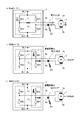
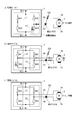
- FIG. 4 shows a current path when the first ground fault occurs
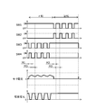
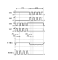
- FIG. 5 shows a time change of the motor current and the short circuit current when the first ground fault occurs.
- the first ground fault is a fault in which an unintended electrical connection occurs with a relatively low impedance between the electric harness 4a of the motor power supply line and the ground. In the motor power supply line, the first ground fault may occur also in the circuit portion between the first IPD 11 and the output terminal 1a or in the circuit portion between the motor terminal 3a and one of the brushes. .
- the electric harness 4a will be described as a representative example of a portion where the first ground fault occurs. The same applies to the following first power supply fault.
- FIG. 6 shows a current path when a second ground fault occurs
- FIG. 7 shows a time change of motor current and short circuit current when a second ground fault occurs.
- the second ground fault is a fault in which an unintended electrical connection occurs with a relatively low impedance between the electric harness 4b of the motor power supply line and the ground.
- a second ground fault may occur also in the circuit portion between the second IPD 12 and the output terminal 1b or the circuit portion between the motor terminal 3b and the other brush in the motor power supply line.
- the electric harness 4b will be described as a representative example of a portion where the second ground fault occurs. The same applies to the following second power supply fault.
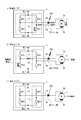
- FIG. 8 shows the current path when the first power supply fault occurs
- FIG. 9 shows the time change of the motor current and the short circuit current when the first power supply fault occurs.
- the first power supply fault is a fault in which an unintended electrical connection occurs with a relatively low impedance between the electric harness 4a of the motor power supply line and the on-board battery B.
- the first power supply fault occurs, in the drive mode M1 shown in FIG. 8A, the current from the on-board battery B flows from the power supply fault point of the electric harness 4a. Then, the current flows from the motor terminal 3a to the motor terminal 3b, and flows to the negative electrode side feed line BL2 through the semiconductor switch SW4. Accordingly, as shown in FIG. 9, a positive motor current flows through the motor 3 and the motor 3 is driven to rotate in the forward direction, so that no short circuit current is generated between the positive electrode of the on-vehicle battery B and the ground.
- FIG. 10 shows a current path when the second power supply fault occurs
- FIG. 11 shows a temporal change of the motor current and the short circuit current when the second power supply fault occurs.
- the second power supply fault is a fault in which an unintended electrical connection occurs with a relatively low impedance between the electric harness 4b of the motor power supply line and the on-board battery B.
- the second power supply fault occurs, in drive mode M1 shown in FIG. 10A, the current from vehicle battery B flows in from the power supply junction of electric harness 4b and passes through semiconductor switch SW4. It flows to the negative electrode side feeder line BL2. Therefore, the motor terminal 3a and the motor terminal 3b have substantially the same potential, and as shown in FIG.
- the motor current is substantially zero in the drive mode M1 and the motor 3 is not driven. Therefore, a short circuit current from the positive electrode of the on-vehicle battery B to the ground flows in the second IPD 12, and the short circuit current is detected as an overcurrent by the overcurrent monitoring unit 12b, and the overcurrent detection signal IS2 from the overcurrent monitoring unit 12b. It is output.
- both the semiconductor switch SW2 and the semiconductor switch SW4 are in the OFF state. Therefore, in drive mode M3, the motor current due to the back electromotive voltage of motor 3 flows back when switched from drive mode M2, but even if the second power supply fault occurs, the current from in-vehicle battery B is It does not flow to the negative electrode side feeder line BL2. That is, in drive mode M3, a short circuit current does not occur between the positive electrode of vehicle battery B and the ground as shown in FIG.
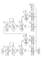
- FIG. 12 shows an example of a main routine of the diagnosis related processing of the motor power supply line, which is executed in the CPU 16 when the ignition switch IGN is turned on and the power supply to the CPU 16 is started.
- step S1 (abbreviated as "S1" in the figure, and so forth), the CPU 16 generates an error in the first IPD 11 or the second IPD 12 based on the overcurrent detection signal IS1 and the overcurrent detection signal IS2. It is determined whether a current is detected. Then, if the CPU 16 determines that the overcurrent is detected (YES), the process proceeds to step S2. On the other hand, when determining that the overcurrent is not detected (NO), the CPU 16 executes step S1 again.
- step S2 the CPU 16 interrupts drive control processing of the motor 3 and executes abnormality diagnosis of the motor power supply line.
- the abnormality diagnosis of the motor power supply line detects and determines whether or not an abnormality occurs in the motor power supply line, including the abnormality aspect.
- the abnormality modes of the motor power supply line include the first ground fault, the second ground fault, the first power fault and the second power fault. Further contents of the abnormality diagnosis will be described later.
- step S3 when the CPU 16 determines the abnormality mode of the motor power supply line by the abnormality diagnosis of step S2 (YES), the process proceeds to step S4. On the other hand, when the abnormality mode of the motor power supply line is not determined (NO), the CPU 16 restarts the drive control process of the motor 3 and returns the process to step S1.
- step S4 the CPU 16 controls the motor 3 to perform a failsafe operation.
- the fail-safe operation includes stopping the operation of the motor 3 and operating the motor 3 only in the rotatable direction.
- the CPU 16 When stopping the operation of the motor 3, the CPU 16 outputs a control signal SIG to the semiconductor relay 13 to turn it off. In addition to or in addition to this, the CPU 16 outputs, to the first IPD 11 and the second IPD 12, an output limit signal INH that forcibly turns off the semiconductor switches SW1 to SW4.
- the CPU 16 When the motor 3 is operated only in the rotatable direction, the CPU 16 performs as follows. That is, the CPU 16 reversely drives the motor 3 when the first ground fault or the second power fault is determined as the abnormal mode of the motor power supply line. Specifically, the CPU 16 sets the pulse width modulation signal PWM1 and the pulse width modulation signal PWM1 such that the on / off setting of the semiconductor switches SW1 to SW4 becomes the drive mode M2 or alternately repeats the drive mode M2 and the drive mode M3. The pulse width modulation signal PWM2 is output. Further, when the second ground fault or the first power-supply fault is determined as the abnormality mode of the motor power supply line, the CPU 16 drives the motor 3 to rotate normally.
- the CPU 16 sets the pulse width modulation signal PWM1 and the pulse width modulation signal PWM1 such that the on / off setting of the semiconductor switches SW1 to SW4 becomes the drive mode M1 or alternately repeats the drive mode M1 and the drive mode M3.
- the pulse width modulation signal PWM2 is output.
- the target VTC angle for fail-safe operation at the time of abnormality is set in advance, and the actual VTC angle is the target as required or forcibly.
- the motor 3 can be driven to achieve the VTC angle.
- the limp home performance is improved by setting the actual VTC angle to a VTC angle that is advantageous to failsafe for the internal combustion engine.
- the CPU 16 stops the operation of the motor 3 when a further abnormality occurs during fail-safe operation in which the motor power supply line is determined to be abnormal and the motor 3 is operated in a rotatable direction as needed. May be For example, when an overcurrent is detected by the overcurrent detection signal IS1 or the overcurrent detection signal IS2 during fail-safe operation, the operation of the motor 3 may be stopped.
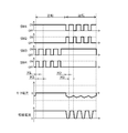
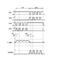
- FIG. 13 is a time chart explaining an abnormality detection method.
- FIG. 13 for example, it is assumed that a first power failure occurs while the motor 3 is driven in normal rotation.
- the CPU 16 drives the motor 3 in the normal direction, the short circuit current is not generated as described above (see FIG. 8A).
- the FB control duty becomes a negative value D2 [%] by the calculation in the CPU 16 and the CPU 16 switches the on / off setting of the semiconductor switches SW1 to SW4 to the drive mode M2 to reversely drive the motor 3, a short circuit current Occurs (see FIG. 8 (b)).
- the short circuit current is detected as an overcurrent by the overcurrent monitoring unit 11b in the first IPD 11, and the overcurrent monitoring signal 11b is output from the overcurrent monitoring unit 11b.
- the on / off setting of the semiconductor switches SW1 to SW4 repeats the driving mode M2 and the driving mode M3 in a short time according to the pulse width modulation signal PWM1, and no short circuit current flows in the on / off setting of the driving mode M3. . Therefore, when the motor 3 is reversely driven, the short circuit current flows only intermittently. Even if the CPU 16 determines the occurrence of the short circuit current when the overcurrent is continuously detected a predetermined number of times in the on / off setting in the drive mode M2, the motor 3 performs the forward rotation and the reverse rotation for a short time. Such repetition is not easy. That is, the overcurrent detected when the on / off setting of the semiconductor switches SW1 to SW4 is set to the drive mode M2 is simply an electrical noise or a short circuit current due to an abnormality in the motor power supply line. It may be difficult to identify the
- the pulse width modulation signal PWM1 and the pulse width modulation signal are forcibly forced as follows regardless of the calculated value of the FB control duty. It outputs PWM2. That is, the CPU 16 forcibly fixes the semiconductor switches SW1 to SW4 to the on / off setting according to at least two different drive modes selected from the drive modes M1 to M3 for a predetermined time, , PWM2 are output. For example, in FIG. 13, the CPU 16 initially fixes the drive mode M2 when detecting an overcurrent.
- the short circuit current flows continuously depending on the on / off setting of the semiconductor switches SW1 to SW4, so the detected overcurrent is a short circuit due to the abnormality in the motor power supply line. It becomes easy to identify that it is a current.
- the CPU 16 generates an abnormality in the motor power supply line based on the detection location (the first IPD 11 or the second IPD 12) of the overcurrent when the predetermined time has elapsed in the on / off setting according to the selected drive mode. Whether or not it has been detected and determined including its abnormal state. For example, as shown in FIG.
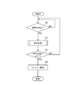
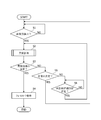
- FIG. 14 shows a first example of a subroutine relating to the abnormality diagnosis of the motor power supply line executed in step S2 of FIG.
- step S11 the CPU 16 forcibly fixes the semiconductor switches SW1 to SW4 to the on / off setting according to the drive mode M1.
- the pulse width modulation signal PWM1 and the pulse width modulation signal PWM2 are used as the first IPD11 and the second IPD12.
- the drive mode may be fixed first. Thereby, the abnormality aspect of the motor power supply line can be detected and determined relatively early.
- step S12 the CPU 16 determines whether or not a predetermined time T1 has elapsed after the semiconductor switches SW1 to SW4 are forcibly fixed to the on / off setting according to the drive mode M1.
- a predetermined time T1 if the first ground fault or the second power fault occurs in the motor power supply line, the semiconductor switches SW1 to SW4 are forcibly fixed in the drive mode M1 to thereby short circuit current. Is a time when it can be clearly determined that
- the predetermined time T1 is a time shorter than the time until the camshaft actually starts the advance operation or the retard operation with respect to the crankshaft by the drive of the motor 3.
- step S13 When the CPU 16 determines that the predetermined time T1 has elapsed (YES), the process proceeds to step S13, whereas when the CPU 16 determines that the predetermined time T1 has not elapsed (NO), the process proceeds to step S12. Run again.
- step S13 the CPU 16 determines whether an overcurrent is detected in the first IPD 11 based on the overcurrent detection signal IS1. Then, if the CPU 16 determines that the overcurrent is detected in the first IPD 11 (YES), the process proceeds to step S14. On the other hand, when the CPU 16 determines that the overcurrent is not detected in the first IPD 11 (NO), the process proceeds to step S15.
- step S14 the CPU 16 detects the occurrence of the first ground fault in the electric harness 4a (see FIG. 4A), determines such an abnormality mode as a result of the abnormality diagnosis, and then ends the present subroutine.
- step S15 the CPU 16 determines whether an overcurrent is detected in the second IPD 12 based on the overcurrent detection signal IS2. Then, when the CPU 16 determines that the overcurrent is detected in the second IPD 12 (YES), the process proceeds to step S16. On the other hand, when the CPU 16 determines that the overcurrent is not detected in the second IPD 12 (NO), the process proceeds to step S17.
- step S16 the CPU 16 detects the occurrence of a second power fault in the electric harness 4b (see FIG. 10A), determines such an abnormality mode as a result of the abnormality diagnosis, and then ends the present subroutine.
- the overcurrent detection determination of the second IPD 12 is performed after the overcurrent detection determination of the first IPD 11 is performed, and the overcurrent detection determination of the second IPD 12 is performed after the overcurrent detection determination of the second IPD 12 is performed.
- Current detection determination may be performed.
- step S17 the CPU 16 outputs a pulse width modulation signal PWM1 and a pulse width modulation signal PWM2 for forcibly fixing the semiconductor switches SW1 to SW4 to the on / off setting according to the drive mode M2.
- step S18 the CPU 16 determines whether or not a predetermined time T2 has elapsed after the semiconductor switches SW1 to SW4 are forcibly fixed to the on / off setting according to the drive mode M2.
- the predetermined time T2 if the second ground fault or the first power fault occurs in the electric harnesses 4a and 4b, the on / off setting of the semiconductor switches SW1 to SW4 is fixed to the drive mode M2. It is a time when it can be clearly determined that the short circuit current is generated.
- the predetermined time T2 is shorter than the time until the camshaft actually starts advancing or retarding with respect to the crankshaft by driving the motor 3.
- the predetermined time T2 may be set to the same time as the predetermined time T1.
- step S19 When the CPU 16 determines that the predetermined time T2 has elapsed (YES), the process proceeds to step S19, whereas when the CPU 16 determines that the predetermined time T2 has not elapsed (NO), the process proceeds to step S18. Run again.
- step S19 the CPU 16 determines whether an overcurrent is detected in the first IPD 11 based on the overcurrent detection signal IS1. Then, when the CPU 16 determines that the overcurrent is detected in the first IPD 11 (YES), the process proceeds to step S20. On the other hand, when the CPU 16 determines that the overcurrent is not detected in the first IPD 11 (NO), the process proceeds to step S21.
- step S20 the CPU 16 detects the occurrence of the first power failure in the electric harness 4a (see FIG. 8B), determines such an abnormality mode as a result of the abnormality diagnosis, and then ends the present subroutine.
- step S21 the CPU 16 determines whether an overcurrent is detected in the second IPD 12 based on the overcurrent detection signal IS2.
- the process proceeds to step S22.
- step S23 the CPU 16 determines in step S21 that the overcurrent is not detected in the second IPD 12 (NO)
- the process proceeds to step S23 to diagnose abnormality as that the motor power supply line is normal. The result of is determined, and this subroutine is ended.
- step S22 the CPU 16 detects the occurrence of the second ground fault in the electric harness 4b (see FIG. 6B), determines such an abnormality mode as a result of the abnormality diagnosis, and then ends the present subroutine.
- the drive mode when the overcurrent is detected is the drive mode M2
- the following may be performed. That is, after the on / off setting of the semiconductor switches SW1 to SW4 is first fixed to the drive mode M2 for the predetermined time T2 and the overcurrent detection is determined, the on / off setting of the semiconductor switches SW1 to SW4 is set to the drive mode M1. It is also possible to fix the predetermined time T1 and determine the overcurrent detection.
- the CPU 16 forcibly fixes the semiconductor switches SW1 to SW4 to the on / off setting according to the drive mode M1, whereby the first ground fault or It can be detected whether or not the power supply fault of 2 has occurred. Further, the CPU 16 forcibly fixes the semiconductor switches SW1 to SW4 to the on / off setting according to the drive mode M2, whereby an abnormality due to the first power fault or the second ground fault is generated in the motor power supply line. It can detect whether it is occurring or not. In short, the CPU 16 can forcibly diagnose the four abnormality modes of the motor power supply line by forcibly fixing the semiconductor switches SW1 to SW4 to the on / off setting according to the relatively small two different drive modes for a predetermined time.
- the motor 3 can be fixed next to the drive mode M2. Slightly reverses. As a result, the rotational position of the motor 3 can be brought close to the state before fixing to the drive mode M1.
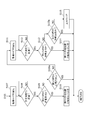
- FIG. 15 shows a second example of a subroutine regarding abnormality diagnosis of the motor power supply line executed in step S2 of FIG.
- step S101 the CPU 16 forcibly fixes the semiconductor switches SW1 to SW4 to the on / off setting according to the drive mode M3.
- the pulse width modulation signal PWM1 and the pulse width modulation signal PWM2 are used as the first IPD11 and the second IPD12.
- the semiconductor switches SW1 to SW4 are forcibly fixed in the drive mode M3 first.
- step S102 the CPU 16 determines whether or not a predetermined time T3 has elapsed after the semiconductor switches SW1 to SW4 are forcibly fixed to the on / off setting according to the drive mode M3. If the first ground fault or the second ground fault has occurred in the motor power supply line, the predetermined time T3 is a short circuit current by forcibly fixing the semiconductor switches SW1 to SW4 to the drive mode M3. Is a time when it can be clearly determined that The predetermined time T3 can be the same as the predetermined times T1 and T2. Alternatively, since motor 3 is not driven in drive mode M3, predetermined time T3 is determined from predetermined times T1 and T2 without considering the time when the camshaft starts advancing or retarding with respect to the crankshaft.
- step S103 When the CPU 16 determines that the predetermined time T3 has elapsed (YES), the process proceeds to step S103, whereas when the CPU 16 determines that the predetermined time T3 has not elapsed (NO), the process proceeds to step S102. Run again.
- step S103 when the CPU 16 determines that the overcurrent is detected in the first IPD 11 (YES), the process proceeds to step S104.
- step S103 when the CPU 16 determines in step S103 that the overcurrent is not detected in the first IPD 11 (NO), the process proceeds to step S105, and the overcurrent is detected in the second IPD 12 Determine if
- step S104 the CPU 16 detects the occurrence of the first ground fault in the electric harness 4a (see FIG. 4C), determines such an abnormality mode as a result of the abnormality diagnosis, and then ends the present subroutine.
- step S105 when the CPU 16 determines that the overcurrent is detected in the second IPD 12 (YES), the process proceeds to step S106.
- step S106 the occurrence of the second ground fault in the electric harness 4b (see FIG. 6C) is detected, and after the result of the abnormality diagnosis is determined in such an abnormal state, the present subroutine is ended.
- step S105 determines in step S105 that no overcurrent is detected in the second IPD 12 (NO), no abnormality due to the first ground fault or the second ground fault has occurred. Then, the process proceeds to step S107. Then, the CPU 16 diagnoses the presence or absence of the first power failure or the second power failure.
- the CPU 16 forcibly fixes the semiconductor switches SW1 to SW4 to the on / off setting according to the drive mode M1 for a predetermined time T1 in steps S107 and S108.
- the CPU 16 proceeds the process to step S109 and determines whether or not an overcurrent is detected in the second IPD 12.
- step S109 when the CPU 16 determines that the overcurrent is detected in the second IPD 12 (YES), the process proceeds to step S110.
- step S110 the CPU 16 detects the occurrence of a second power fault in the electric harness 4b (see FIG. 10A), determines such an abnormal state as a result of abnormality diagnosis, and then ends the present subroutine.
- the CPU 16 does not perform the determination of the overcurrent detection in the first IPD 11 when the predetermined time T1 elapses by fixing the drive mode M1 in step S107. This is because when the semiconductor switches SW1 to SW4 are forcibly fixed to the on / off setting according to the drive mode M3 in step S101, the occurrence of the first ground fault is not detected by the execution of step S103. It is.
- step S109 when the CPU 16 determines that the overcurrent is not detected in the second IPD 12 (NO), the process proceeds to step S111.
- the CPU 16 forcibly fixes the semiconductor switches SW1 to SW4 to the on / off setting according to the drive mode M2 for a predetermined time T2 in steps S111 and S112.
- the CPU 16 proceeds the process to step S113 to determine whether or not the overcurrent is detected in the first IPD 11.
- step S113 when the CPU 16 determines that the overcurrent is detected in the first IPD 11 (YES), the process proceeds to step S114.
- step S114 the CPU 16 detects the occurrence of the first power failure in the electric harness 4a (see FIG. 8B), determines such an abnormal state as a result of the abnormality diagnosis, and ends the present subroutine.
- step S115 the CPU 16 determines in step S113 that no overcurrent is detected in the first IPD 11 (NO)
- the process proceeds to step S115 to diagnose abnormality as that the motor power supply line is normal. The result of is determined, and this subroutine is ended.
- the CPU 16 does not perform the determination of the overcurrent detection in the second IPD 12 when the predetermined time T2 elapses by fixing the drive mode M2 in step S111. This is because when the semiconductor switches SW1 to SW4 are forcibly fixed in the on / off setting according to the drive mode M3 in step S101, the occurrence of the second ground fault has not been detected by the execution of step S105. It is.
- the CPU 16 first fixes the semiconductor switches SW1 to SW4 to the on / off setting according to the drive mode M3. Therefore, the CPU 16 can first detect the occurrence of the first ground fault and the second ground fault having a relatively high frequency of occurrence. Further, even if the CPU 16 does not detect the occurrence of the first ground fault and the second ground fault, the semiconductor switches SW1 to SW4 are forcibly set to the on / off setting according to the drive mode M1 or the drive mode M2. By fixing to, it is possible to detect the occurrence of the first power failure and the second power failure.
- FIG. 16 shows a third example of a subroutine regarding abnormality diagnosis of the motor power supply line executed in step S2 of FIG.
- Steps S201 to S212 in this subroutine have the same contents as steps S11 to S22 in FIG. 14, and steps S213 to S218 have the same contents as steps S101 to S106 in FIG. 15, respectively. Therefore, the detailed description of each step will be omitted or simplified, except for the following differences.
- the CPU 16 forcibly fixes the semiconductor switches SW1 to SW4 to the on / off setting according to the drive mode M1 at the predetermined time T1 in steps S201 and S202. Then, even if the CPU 16 detects the occurrence of the first ground fault in step S204 or detects the occurrence of the second power fault in step S206, the abnormality mode is immediately determined as a result of the abnormality diagnosis. Continue this subroutine without.
- the CPU 16 temporarily stores the detection result regarding the abnormal state detected in step S204 or step S206 in a storage unit such as a random access memory (RAM).
- the CPU 16 advances the process to step S207 to forcibly fix the semiconductor switches SW1 to SW4 to the on / off setting according to the drive mode M2 and to perform abnormality diagnosis.
- the CPU 16 does not detect the overcurrent of the second IPD 12 in step S205 (NO)
- step S207 and S208 the CPU 16 forcibly fixes the semiconductor switches SW1 to SW4 to the on / off setting according to the drive mode M2 for a predetermined time T2. Then, even if the CPU 16 detects the occurrence of the first power supply fault in step S210 or detects the occurrence of the second ground fault in step S212, the abnormality mode is immediately determined as a result of the abnormality diagnosis. Continue this subroutine without.
- the CPU 16 temporarily stores the detection result regarding the abnormal state detected in step S210 or step S212 in a storage unit such as a RAM.
- step S213 to forcibly fix the semiconductor switches SW1 to SW4 to the on / off setting according to the drive mode M3 and to perform abnormality diagnosis.
- the CPU 16 does not detect the overcurrent of the second IPD 12 in step S211 (NO)
- the process proceeds to step S213.
- the CPU 16 forcibly fixes the semiconductor switches SW1 to SW4 to the on / off setting according to the driving mode M3 for a predetermined time T3 in steps S213 and S214. Then, even if the CPU 16 detects the occurrence of the first ground fault in step S216 or detects the occurrence of the second ground fault in step S218, the abnormality mode is immediately determined as a result of the abnormality diagnosis. Continue this subroutine without.
- the CPU 16 temporarily stores the detection result regarding the abnormal mode detected in step S216 or step S218 in the storage means such as the RAM, and advances the process to step S219.
- the CPU 16 does not detect the overcurrent of the second IPD 12 in step S 217 (NO), it temporarily stores the detection result that the occurrence of the first ground fault and the second ground fault is not detected. Then, the process proceeds to step S219.
- step S219 the CPU 16 determines whether or not an abnormality has occurred in the motor power supply line based on all detection results temporarily stored in the storage unit such as the RAM by the abnormality diagnosis of the present subroutine. Determine including the aspect.
- the CPU 16 determines the result of the abnormality diagnosis assuming that the motor power supply line is normal, and this subroutine Finish.
- step S219 when the detection result temporarily stored in the storage unit such as the RAM indicates one type of abnormality mode in step S219, the CPU 16 determines the abnormality mode as a result of the abnormality diagnosis, and the subroutine Finish.
- the CPU 16 detects the occurrence of the first ground fault in step S204 and also detects the occurrence of the first ground fault in step S216, the storage means such as the RAM has one type of abnormality mode. The detection result shown is stored. Therefore, CPU 16 determines the first ground fault as a result of the abnormality diagnosis of the motor power supply line in step S219.
- step S219 CPU 16 does not determine the result of the abnormality diagnosis of the motor power supply line when the detection result temporarily stored in the storage unit such as the RAM indicates two or more types of abnormality modes. End this subroutine.
- the motor drive control device 1 when the CPU 16 of the motor drive control device 1 detects an overcurrent, the semiconductor switches SW1 to SW4 are set to ON / OFF settings according to at least two drive modes appropriately selected from drive modes M1 to M3 for a predetermined time. It is fixed forcibly. Therefore, when an abnormality occurs in the motor power supply line, depending on the on / off setting of the semiconductor switches SW1 to SW4, a short circuit current continuously flows according to the abnormality mode.
- the CPU 16 It becomes easy to detect whether or not the abnormality is included.
- the subroutine has ended. In this case, the process returns from step S3 to step S1 in the main routine of FIG. 12 to resume the drive control process of the motor 3.
- diagnosis related is performed again to determine the diagnosis result without performing the drive control processing of the motor 3 as described below.
- the main routine of the process (see FIG. 12) may be modified.
- FIG. 17 shows a modification of the main routine (see FIG. 12) of the diagnosis related processing.
- the following steps S5 and S6 are added to FIG.
- the description of steps (steps S1 to S4) having the same reference numerals as in FIG. 12 will be omitted or simplified.
- step S3 CPU16 advances a process to step S5, when the abnormality aspect of a motor electric power supply line is not determined (NO).
- step S5 when the CPU 16 determines that the motor power supply line is normal as a result of the abnormality diagnosis in step S2 (YES), the CPU 16 resumes the drive control process of the motor 3 and returns the process to step S1.
- the CPU 16 advances the process to step S6.
- step S6 the CPU 16 determines whether or not a time set in advance as a time from when the abnormality diagnosis is performed in step S2 to when the abnormality diagnosis is performed again, that is, a rediagnosis waiting time has elapsed.
- the CPU 16 determines that the rediagnosis waiting time has elapsed (YES)
- the CPU 16 advances the process to step S2 to perform abnormality diagnosis again.
- the CPU 16 determines that the rediagnosis waiting time has not elapsed (NO)
- the CPU 16 executes step S6 again.
- step S2 If the abnormality mode of the motor power supply line can not be determined even if the abnormality diagnosis in step S2 is continuously performed a plurality of times, the CPU 16 resumes the drive control process of the motor 3 and proceeds to step S5. Then, the process may immediately return to step S1.
- the abnormality diagnosis of the motor power supply line in step S2 in FIG. 12 or 17 is performed when an overcurrent is detected in the first IPD 11 or the second IPD 12 while driving the motor 3 in step S1. It has been described as being implemented. However, the abnormality diagnosis of the motor power supply line is not limited to the timing at which the overcurrent is detected, and may be performed at the next timing.
- step S1a the CPU 16 performs step S1a of FIG. 18 instead of step S1 of FIG. 12 or FIG. 17 to determine whether or not a feedback abnormality has occurred when performing drive control processing of the motor 3 Can be determined.
- step S1a when the CPU 16 determines that a feedback abnormality has occurred (YES), the drive control process of the motor 3 is interrupted, and the process proceeds to step S2 to diagnose an abnormality in the motor power supply line. It can be performed. Whether or not the feedback abnormality is present can be diagnosed based on, for example, whether or not a state where the target VTC angle and the actual VTC angle deviate by a predetermined amount lasts for a predetermined time.
- step S1a NO
- the CPU 16 executes step S1a again.
- FIG. 19 is a flowchart of FIG. 17 except that step S1 for determining the overcurrent detection is deleted and step S7 for starting the drive control process of the motor 3 is added. That is, when the normality of the motor power supply line has already been determined as a result of the abnormality diagnosis in step S2, CPU 16 advances the process from step S5 to step S7 (YES), and performs the drive control process of motor 3 Start. On the other hand, if the CPU 16 does not determine the normality of the motor power supply line as a result of the abnormality diagnosis in step S2, the process proceeds from step S5 to step S6 (NO). It is determined whether or not. If the CPU 16 determines in step S6 that the rediagnosis waiting time has elapsed (YES), the CPU 16 returns to step S2 to perform abnormality diagnosis again.
- step S109a of performing determination of overcurrent detection in the first IPD 11 with respect to the flowchart of FIG. 15 and overcurrent detection in the second IPD 12 Step S113a which performs determination may be added.
- step S109a When the CPU 16 detects an overcurrent in the first IPD 11 at step S109a (YES), the CPU 16 detects the occurrence of a first ground fault (see FIG. 4A). However, even if the semiconductor switches SW1 to SW4 are forcibly fixed to the on / off setting according to the drive mode M3 in step S101, the execution of step S103 does not detect the occurrence of the first ground fault. For this reason, since the detection result is that wrinkles have occurred, the CPU 16 ends the abnormality diagnosis subroutine without determining the abnormality mode when the overcurrent in the first IPD 11 is detected in step S109a. . On the other hand, when the CPU 16 does not detect the overcurrent in the first IPD 11 in step S109a (NO), the CPU 16 advances the process to step S111.
- step S113a When the CPU 16 detects an overcurrent in the second IPD 12 at step S113a (YES), the CPU 16 detects the occurrence of a second ground fault (see FIG. 6B). However, even if the semiconductor switches SW1 to SW4 are forcibly fixed to the on / off setting according to the drive mode M3 in step S101, the execution of step S105 does not detect the occurrence of the second ground fault. For this reason, since the detection result indicates that the detection result is false, when the CPU 16 detects an overcurrent in the second IPD 12 in step S113a, the abnormality diagnosis subroutine is ended without determining the abnormality.
- step S113a the process proceeds to step S115, and the result of abnormality diagnosis is determined as that the motor power supply line is normal. Then, the abnormality diagnosis subroutine is ended.
- SYMBOLS 1 Motor drive control apparatus, 3 ... Motor, 4a, 4b ... Electric harness, 11 ... 1st IPD, 11a ... Signal control part, 11b ... Overcurrent monitoring part, 12 ... 2nd IPD, 12a ... Signal control part 12b: Overcurrent monitoring unit 16: CPU, SW1 to SW4: Semiconductor switch, PWM1: Pulse width modulation signal, PWM2: Pulse width modulation signal, IS1: Overcurrent detection signal, IS2: Overcurrent detection signal, M1 to M3 ... Drive mode, T1 to T3 ... Predetermined time
Landscapes
- Engineering & Computer Science (AREA)
- Power Engineering (AREA)
- Control Of Electric Motors In General (AREA)
- Control Of Direct Current Motors (AREA)
Abstract
モータ駆動制御部は、モータに供給する電力を調整する複数の半導体スイッチSW1~SW4を備えた駆動部と、複数の半導体スイッチSW1~SW4のオン・オフ状態を制御する制御信号PWM1,PWM2を駆動部に出力する制御部と、駆動部における過電流を複数箇所で監視する過電流監視部と、を備える。制御部は、所定のタイミングで、複数の半導体スイッチを強制的に少なくとも2つの異なるオン・オフ設定(M2)で所定時間ずつ固定する制御信号を駆動部に出力し、所定時間が経過するたびに、駆動部における過電流の検出箇所に基づいて、駆動部からモータまでのモータ電力供給線において地絡又は天絡による異常が発生しているか否かを検知する異常検知を行う。
Description
本発明は、モータ駆動制御装置及びモータ電力供給線の異常検知方法に関する。
従来のモータ駆動制御装置としては、例えば特許文献1に記載されているように、車両用内燃機関の可変バルブタイミング機構において、クランクシャフトとカムシャフトとの回転位相差を調整するためにカムシャフトを回転させるモータの駆動部として、いわゆるHブリッジ回路を備えたモータ駆動制御装置が知られている。
ところで、モータ駆動制御装置における駆動部からモータまでのモータ電力供給線に地絡・天絡による異常が発生した場合に、かかる異常に起因した短絡電流は、Hブリッジ回路における半導体スイッチのオン・オフ設定が一定の状態で継続する。このため、クランクシャフトとカムシャフトとの回転位相差を目標値に追従させるために、Hブリッジ回路における半導体スイッチがオン・オフを繰り返し、あるいは、モータが正転・逆転を短時間で繰り返すと、短絡電流が継続的に流れないことがある。したがって、モータ駆動制御装置が過電流を検出したとしても、検出された過電流が、単なる電気的ノイズによるものであるのか、あるいは、モータ電力供給線の異常による短絡電流であるのか否かの判断が困難となるおそれがある。
そこで、本発明は以上のような問題点に鑑み、モータ電力供給線における異常の検知を容易にするモータ駆動制御装置及びモータ電力供給線の異常検知方法を提供することを目的とする。
このため、本発明に係るモータ駆動制御装置は、モータに供給する電力を調整する複数の半導体スイッチを備えた駆動部と、複数の半導体スイッチのオン・オフ状態を制御する制御信号を駆動部に出力する制御部と、駆動部における過電流を複数箇所で監視する過電流監視部と、を備え、制御部は、所定のタイミングで、複数の半導体スイッチを強制的に少なくとも2つの異なるオン・オフ設定で所定時間ずつ固定する制御信号を駆動部に出力し、所定時間が経過するたびに、駆動部における過電流の検出箇所に基づいて、駆動部からモータまでのモータ電力供給線において地絡又は天絡による異常が発生しているか否かを検知する異常検知を行う。
また、本発明に係るモータ電力供給線の異常検知方法は、モータに供給する電力を調整する複数の半導体スイッチを備えた駆動部からモータまでのモータ電力供給線の異常を検知するものであって、所定のタイミングで、複数の半導体スイッチを少なくとも2つの異なるオン・オフ設定で所定時間ずつ強制的に固定する制御信号を駆動部に出力し、駆動部における過電流を複数箇所で監視し、所定時間が経過するたびに、駆動部における過電流の検出箇所に基づいて、モータ電力供給線において地絡又は天絡による異常が発生しているか否かを検知する。
本発明のモータ駆動制御装置及びモータ電力供給線の異常検知方法によれば、モータ電力供給線における異常の検知を容易ならしめることができる。
以下、添付された図面を参照し、本発明を実施するための実施形態について詳述する。
図1は、本発明に係るモータ駆動制御装置の一例を示す。
図1は、本発明に係るモータ駆動制御装置の一例を示す。
[モータ駆動制御装置の内部構成]
モータ駆動制御装置1は、CAN(Controller Area Network)等によって通信可能に接続された上位制御装置であるECM(Electric Control Module)2からの指令信号に基づいて、直流整流子電動機であるモータ3を駆動制御する。モータ3とモータ駆動制御装置1とは、互いに別体に構成され、電気ハーネス4a,4bによって接続されている。
モータ駆動制御装置1は、CAN(Controller Area Network)等によって通信可能に接続された上位制御装置であるECM(Electric Control Module)2からの指令信号に基づいて、直流整流子電動機であるモータ3を駆動制御する。モータ3とモータ駆動制御装置1とは、互いに別体に構成され、電気ハーネス4a,4bによって接続されている。
本実施形態では、モータ3は、内燃機関においてバルブタイミングを連続的に変更する可変バルブタイミング機構に備えられる。モータ3は、クランクシャフトの回転位相に対してカムシャフトの回転位相を進角又は遅角するために、すなわちVTC(Valve Timing Control)角度を制御量として制御するために、カムシャフトを回転駆動する駆動アクチュエータとして用いられる。ただし、モータ3は、可変バルブタイミング機構に限らず、他の車載システムにおける駆動アクチュエータにも利用できる。例えば、モータ3は、ピストンの上死点位置を変化させて圧縮比を変更する圧縮比可変機構や、吸気バルブのリフト量及び開弁期間を変更する可変動弁機構等に利用可能である。
モータ駆動制御装置1は、直流電源である車載バッテリBから供給された直流電力をモータ3へ供給する電力に調整する駆動部として、第1のインテリジェント・パワー・デバイス11及び第2のインテリジェント・パワー・デバイス12を備えている。以下、第1のインテリジェント・パワー・デバイス11を第1のIPD11と略記し、第2のインテリジェント・パワー・デバイス12を第2のIPD12と略記する。第1のIPD11及び第2のIPD12は、車載バッテリBの正極と接続される正極側給電線BL1と車載バッテリBの負極と接続される負極側給電線BL2との間に並列に接続される。第1のIPD11は、モータ駆動制御装置1の出力端子1aを介して電気ハーネス4aによりモータ3の一方のモータ端子3aと接続される。また、第2のIPD12は、モータ駆動制御装置1の出力端子1bを介して電気ハーネス4bによりモータ3の他方のモータ端子3bと接続される。
正極側給電線BL1には、半導体リレー13および平滑回路14が介装されている。半導体リレー13は、外部からの制御信号SIGを入力することでオン・オフ制御可能に構成され、オン状態では、第1のIPD11及び第2のIPD12へ電力を供給し、オフ状態では、第1のIPD11及び第2のIPD12に対する電力の供給を遮断する。平滑回路14は、車載バッテリBから供給される電力の交流成分を低減する回路であり、例えば図示のように、正極側給電線BL1に介装されたコイル14aと、その各端部とグランドを接続する2つのコンデンサ14bと、を有するπ型フィルタで構成される。
モータ駆動制御装置1は、その内部に有する電源回路15を電源供給源として、モータ3の駆動制御処理を実行するCPU(Central Processing Unit)16を制御部として内蔵している。電源回路15には、イグニッションスイッチIGNがオン状態であるときに、車載バッテリBから電力が供給される。
CPU16は、ECM2からの指令信号に基づいて、VTC角度の目標値である目標VTC角度を決定する。また、CPU16は、クランクシャフトの回転位相を検出するクランク角センサ17からの出力信号Scrank及びカムシャフトの回転位相を検出するカム角センサ18からの出力信号Scamに基づいて、実際のVTC角度を演算する。そして、CPU16は、目標VTC角度と実際のVTC角度との偏差に基づいて、第1のIPD11に出力するパルス幅変調信号PWM1のデューティ及び第2のIPD12に出力するパルス幅変調信号PWM2のデューティを決定する。そして、CPU16は、決定したデューティを反映したパルス幅変調信号PWM1,PWM2を、第1のIPD11及び第2のIPD12へそれぞれ出力し、これにより、フィードバック(FB)制御が行われる。
CPU16は、モータ3の駆動制御処理に加えて、後述するように、第1のIPD11からの過電流検出信号IS1と第2のIPD12からの過電流検出信号IS2とに基づいて、診断関連処理を実行する。診断関連処理は、第1のIPD11及び第2のIPD12からモータ3までのモータ電力供給線における異常診断を行うための処理である。モータ電力供給線は、電気ハーネス4a,4bに加え、以下を含む概念である。すなわち、モータ電力供給線は、モータ駆動制御装置1において第1のIPD11から出力端子1aまでの回路部分及び第2のIPD12から出力端子1bまでの回路部分を含む。また、モータ電力供給線は、モータ3においてモータ端子3aから一方のブラシまでの回路部分及びモータ端子3bから他方のブラシまでの回路部分を含む。CPU16は、異常診断の結果に基づいて、半導体リレー13に対して、これをオフ状態にする制御信号SIGを出力するように構成される。また、CPU16は、第1のIPD11及び第2のIPD12に対して、第1のIPD11及び第2のIPD12からモータ3に対する電力供給を遮断する出力制限信号INHを出力するように構成されている。
[IPDの内部構成]
図2は、モータ駆動制御装置におけるIPDの内部構成を示す。図2に示すように、第1のIPD11は、正極側給電線BL1と負極側給電線BL2との間で直列に接続される半導体スイッチSW1及び半導体スイッチSW2を有している。同様に、第2のIPD12は、正極側給電線BL1と負極側給電線BL2との間で直列に接続される半導体スイッチSW3及び半導体スイッチSW4を有している。半導体スイッチSW1~SW4には、例えばバイポーラトランジスタや電界効果型トランジスタ等の各種半導体スイッチング素子を用い得る。半導体スイッチSW1,SW2のオン・オフ状態はCPU16から第1のIPD11に出力された制御信号であるパルス幅変調信号PWM1に基づいて制御される。また、半導体スイッチSW3,SW4のオン・オフ状態はCPU16から第2のIPD12に出力された制御信号であるパルス幅変調信号PWM2に基づいて制御される。
図2は、モータ駆動制御装置におけるIPDの内部構成を示す。図2に示すように、第1のIPD11は、正極側給電線BL1と負極側給電線BL2との間で直列に接続される半導体スイッチSW1及び半導体スイッチSW2を有している。同様に、第2のIPD12は、正極側給電線BL1と負極側給電線BL2との間で直列に接続される半導体スイッチSW3及び半導体スイッチSW4を有している。半導体スイッチSW1~SW4には、例えばバイポーラトランジスタや電界効果型トランジスタ等の各種半導体スイッチング素子を用い得る。半導体スイッチSW1,SW2のオン・オフ状態はCPU16から第1のIPD11に出力された制御信号であるパルス幅変調信号PWM1に基づいて制御される。また、半導体スイッチSW3,SW4のオン・オフ状態はCPU16から第2のIPD12に出力された制御信号であるパルス幅変調信号PWM2に基づいて制御される。
第1のIPD11における半導体スイッチSW1と半導体スイッチSW2との間は、モータ3の一方のモータ端子3aと接続されている。また、第2のIPD12における半導体スイッチSW3と半導体スイッチSW4との間は、モータ3の他方のモータ端子3bと接続されている。これにより、第1のIPD11の半導体スイッチSW1及び半導体スイッチSW2、並びに第2のIPD12の半導体スイッチSW3及び半導体スイッチSW4は、それぞれ上下アームを形成している。そして、第1のIPD11及び第2のIPD12は、半導体スイッチSW1~SW4によって、モータ3を正転方向及び逆転方向に回転駆動可能なHブリッジ回路を構成している。
第1のIPD11は、CPU16から入力したパルス幅変調信号PWM1に基づいて、半導体スイッチSW1及び半導体スイッチSW2に制御信号P1,P2を出力する信号制御部11aを有している。具体的には、信号制御部11aは、下アームの半導体スイッチSW2へパルス幅変調信号PWM1に相当する制御信号P2を出力するとともに、上アームの半導体スイッチSW1へパルス幅変調信号PWM1を反転した信号に相当する制御信号P1を出力する。また、信号制御部11aは、CPU16から入力した出力制限信号INHに基づいて、パルス幅変調信号PWM1にかかわらず、半導体スイッチSW1及び半導体スイッチSW2のいずれも強制的にオフ状態にする制御信号P1,P2を出力する。
同様に、第2のIPD12は、CPU16から入力したパルス幅変調信号PWM2に基づいて、半導体スイッチSW3及び半導体スイッチSW4に制御信号P3,P4を出力する信号制御部12aを有している。具体的には、信号制御部12aは、下アームの半導体スイッチSW4へパルス幅変調信号PWM2に相当する制御信号P4を出力するとともに、上アームの半導体スイッチSW3へパルス幅変調信号PWM2を反転した信号に相当する制御信号P3を出力する。また、信号制御部12aは、CPU16から入力した出力制限信号INHに基づいて、パルス幅変調信号PWM2にかかわらず、半導体スイッチSW3及び半導体スイッチSW4のいずれも強制的にオフ状態にする制御信号P3,P4を出力する。
第1のIPD11は、半導体スイッチSW1及び半導体スイッチSW2における過電流を監視するように構成された過電流監視部11bを有している。第2のIPD12は、半導体スイッチSW3及び半導体スイッチSW4における過電流を監視するように構成された過電流監視部12bを有している。過電流監視部11bは第1のIPD11において過電流を検出したときにCPU16に対して過電流検出信号IS1を出力し、過電流監視部12bは第2のIPD12において過電流を検出したときにCPU16に対して過電流検出信号IS2を出力する。
[モータの駆動制御処理]
図3は、モータの駆動制御処理における各種パラメータの時間変化を示す。CPU16は、モータ3の駆動制御処理において、PI(Proportional-Integral)制御等を用いて、実際のVTC角度(制御量)と目標VTC角度(制御量の目標値)との偏差に基づいてFB制御デューティを演算する。FB制御デューティは、半導体スイッチSW1~SW4のそれぞれがオン及びオフを繰り返すスイッチングにおいて、オン時間の比率を示す百分率である。実際のVTC角度が目標VTC角度よりも小さい場合、FB制御デューティは、例えば、正の値D1[%]として算出される。一方、実際のVTC角度が目標VTC角度よりも大きい場合、FB制御デューティは、例えば、負の値D2[%]として算出される。
図3は、モータの駆動制御処理における各種パラメータの時間変化を示す。CPU16は、モータ3の駆動制御処理において、PI(Proportional-Integral)制御等を用いて、実際のVTC角度(制御量)と目標VTC角度(制御量の目標値)との偏差に基づいてFB制御デューティを演算する。FB制御デューティは、半導体スイッチSW1~SW4のそれぞれがオン及びオフを繰り返すスイッチングにおいて、オン時間の比率を示す百分率である。実際のVTC角度が目標VTC角度よりも小さい場合、FB制御デューティは、例えば、正の値D1[%]として算出される。一方、実際のVTC角度が目標VTC角度よりも大きい場合、FB制御デューティは、例えば、負の値D2[%]として算出される。
CPU16は、FB制御デューティが正の値D1[%]として算出された場合、パルス幅変調信号PWM1のデューティを0[%]に決定しつつ、パルス幅変調信号PWM2のデューティをD1[%]に決定する。一方、CPU16は、FB制御デューティが負の値D2[%]として算出された場合、パルス幅変調信号PWM2のデューティを0[%]に決定しつつ、パルス幅変調信号PWM1のデューティをD2[%]の絶対値に決定する。そして、CPU16は、決定したデューティを反映したパルス幅変調信号PWM1,PWM2を、それぞれ、第1のIPD11及び第2のIPD12へ出力する。
第1のIPD11において、信号制御部11aは、デューティが0[%]に決定されたパルス幅変調信号PWM1を入力すると、制御信号P1及び制御信号P2を以下のように出力する。すなわち、信号制御部11aは、上アームの半導体スイッチSW1に対して、デューティを100[%]にした制御信号P1を出力し、下アームの半導体スイッチSW2に対して、デューティを0[%]にした制御信号P2を出力する。一方、信号制御部11aは、デューティがD2[%]の絶対値に決定されたパルス幅変調信号を入力すると、制御信号P1及び制御信号P2を以下のように出力する。すなわち、信号制御部11aは、上アームの半導体スイッチSW1に対して、デューティを(100-|D2|)[%]にした制御信号P1を出力し、下アームの半導体スイッチSW2に対して、デューティをD2[%]の絶対値にした制御信号P2を出力する。半導体スイッチSW1及び半導体スイッチSW2は、一方がオン状態であるとき他方がオフ状態となる相補PWM(Pulse Width Modulation)で制御される。
第2のIPD12において、信号制御部12aは、デューティがD1[%]に決定されたパルス幅変調信号PWM2を入力すると、制御信号P3及び制御信号P4を以下のように出力する。すなわち、信号制御部12aは、上アームの半導体スイッチSW3に対して、デューティを(100-D1)[%]にした制御信号P3を出力し、下アームの半導体スイッチSW4に対して、デューティをD1[%]にした制御信号P4を出力する。一方、信号制御部12aは、デューティが0[%]に決定されたパルス幅変調信号PWM2を入力すると、制御信号P3及び制御信号P4を以下のように出力する。すなわち、信号制御部12aは、上アームの半導体スイッチSW3に対して、デューティを100[%]にした制御信号P3を出力し、下アームの半導体スイッチSW4に対して、デューティを0[%]にした制御信号P4を出力する。半導体スイッチSW3及び半導体スイッチSW4は、一方がオン状態であるとき他方がオフ状態となる相補PWMで制御される。
FB制御デューティが正の値D1[%]のときに、半導体スイッチSW1~SW4のオン・オフ状態が以下のようになる場合を駆動モードM1という。すなわち、第1のIPD11における上アームの半導体スイッチSW1がオン状態であり、かつ、第2のIPD12における下アームの半導体スイッチSW4がオン状態である場合を、駆動モードM1という。駆動モードM1では、車載バッテリBからの電流は、正極側給電線BL1から半導体スイッチSW1を通り、モータ3をモータ端子3aからモータ端子3bに向けて流れ、半導体スイッチSW4を通って負極側給電線BL2に流れる。駆動モードM1のときモータ3に流れるモータ電流を正の値とし、モータ3は正方向に回転(正転)するものとする。
一方、FB制御デューティが負の値D2[%]のときに、半導体スイッチSW1~SW4のオン・オフ状態が以下のようになる場合を駆動モードM2という。すなわち、第2のIPD12における上アームの半導体スイッチSW3がオン状態であり、かつ、第1のIPD11における下アームの半導体スイッチSW2がオン状態である場合を、駆動モードM2という。駆動モードM2では、車載バッテリBからの電流は、正極側給電線BL1から半導体スイッチSW3を通り、モータ3をモータ端子3bからモータ端子3aに向けて流れ、半導体スイッチSW2を通って負極側給電線BL2に流れる。駆動モードM2のときモータ3に流れるモータ電流を負の値とし、モータ3は逆方向に回転(逆転)するものとする。
半導体スイッチSW1~SW4のオン・オフ設定が駆動モードM1である場合に、半導体スイッチSW4がパルス幅変調信号PWM2に応じてオン状態からオフ状態に変化すると、半導体スイッチSW3は相補PWM制御によってオフ状態からオン状態に変化する。この変化後の半導体スイッチSW1~SW4のオン・オフ設定を駆動モードM3という。このときの駆動モードM3では、逆起電圧によりモータ3をモータ端子3aからモータ端子3bに向けて流れようとするモータ電流は、第2のIPD12の半導体スイッチSW3を通って正極側給電線BL1から第1のIPD11の半導体スイッチSW1を通る。そして、かかる逆起電圧によるモータ電流は、モータ3のモータ端子3aに流れて還流することで、徐々に低減する。これにより、モータ3の逆起電圧に起因した半導体スイッチSW1~SW4等の故障を抑制している。
半導体スイッチSW1~SW4のオン・オフ設定が駆動モードM2である場合に、半導体スイッチSW2がパルス幅変調信号PWM1に応じてオン状態からオフ状態に変化すると、半導体スイッチSW1が相補PWM制御によってオフ状態からオン状態に変化する。この変化後の半導体スイッチSW1~SW4のオン・オフ設定も上記の駆動モードM3となる。このときの駆動モードM3では、逆起電圧によりモータ3をモータ端子3bからモータ端子3aに向けて流れようとするモータ電流は、第1のIPD11の半導体スイッチSW1を通って正極側給電線BL1から第2のIPD12の半導体スイッチSW3を通る。そして、かかる逆起電圧によるモータ電流は、モータ3のモータ端子3bに流れて還流することで、徐々に低減する。これにより、モータ3の逆起電圧に起因した半導体スイッチSW1~SW4等の故障を抑制している。
[モータ電力供給線の異常態様]
次に、モータ電力供給線の診断関連処理について説明する前に、モータ電力供給線の異常態様と各態様におけるモータ電流及び短絡電流とについて、図4~図11を用いて説明する。モータ電力供給線の異常態様としては、後述するように、第1の地絡故障、第2の地絡故障、第1の天絡故障及び第2の天絡故障がある。
次に、モータ電力供給線の診断関連処理について説明する前に、モータ電力供給線の異常態様と各態様におけるモータ電流及び短絡電流とについて、図4~図11を用いて説明する。モータ電力供給線の異常態様としては、後述するように、第1の地絡故障、第2の地絡故障、第1の天絡故障及び第2の天絡故障がある。
(第1の地絡故障)
図4は第1の地絡故障が発生している場合の電流経路を示し、図5は第1の地絡故障が発生している場合のモータ電流及び短絡電流の時間変化を示す。第1の地絡故障は、モータ電力供給線のうち電気ハーネス4aとグランドとの間において、比較的低いインピーダンスで意図しない電気的な接続が発生する故障である。なお、モータ電力供給線のうち、第1のIPD11と出力端子1aとの間の回路部分、又は、モータ端子3aと一方のブラシとの間の回路部分でも第1の地絡故障は発生し得る。ただし、以下では、電気ハーネス4aを第1の地絡故障が発生する箇所の代表例として説明する。下記の第1の天絡故障についても同様である。
図4は第1の地絡故障が発生している場合の電流経路を示し、図5は第1の地絡故障が発生している場合のモータ電流及び短絡電流の時間変化を示す。第1の地絡故障は、モータ電力供給線のうち電気ハーネス4aとグランドとの間において、比較的低いインピーダンスで意図しない電気的な接続が発生する故障である。なお、モータ電力供給線のうち、第1のIPD11と出力端子1aとの間の回路部分、又は、モータ端子3aと一方のブラシとの間の回路部分でも第1の地絡故障は発生し得る。ただし、以下では、電気ハーネス4aを第1の地絡故障が発生する箇所の代表例として説明する。下記の第1の天絡故障についても同様である。
第1の地絡故障が発生している場合、図4(a)に示す駆動モードM1及び図4(c)に示す駆動モードM3では、車載バッテリBからの電流は、正極側給電線BL1から半導体スイッチSW1を経て電気ハーネス4aの地絡箇所からグランドへと直接流れる。このため、図5に示すように、駆動モードM1、及び、駆動モードM1から切り換わったときの駆動モードM3ではモータ電流は略零となり、モータ3は駆動されない。また、駆動モードM2から切り換わったときの駆動モードM3では、モータ3の逆起電圧によってモータ電流が流れるものの、車載バッテリBからの電流は、モータ3の逆起電圧によってモータ3には流れず、モータ3の駆動には寄与しない。したがって、第1のIPD11には車載バッテリBの正極からグランドに向かう短絡電流が流れ、この短絡電流は過電流監視部11bにより過電流として検出され、過電流監視部11bから過電流検出信号IS1が出力される。
また、第1の地絡故障が発生している場合、図4(b)に示す駆動モードM2では、車載バッテリBからの電流は、正極側給電線BL1から半導体スイッチSW3を通って、モータ3をモータ端子3bからモータ端子3aに向って流れ、電気ハーネス4aの地絡箇所からグランドへ流れる。したがって、モータ3には、図5に示すように負のモータ電流が流れて、モータ3が逆転駆動されるため、車載バッテリBの正極とグランドとの間に短絡電流は発生しない。
(第2の地絡故障)
図6は第2の地絡故障が発生している場合の電流経路を示し、図7は第2の地絡故障が発生している場合のモータ電流及び短絡電流の時間変化を示す。第2の地絡故障は、モータ電力供給線のうち電気ハーネス4bとグランドとの間において、比較的低いインピーダンスで意図しない電気的な接続が発生する故障である。なお、モータ電力供給線のうち、第2のIPD12と出力端子1bとの間の回路部分、又は、モータ端子3bと他方のブラシとの間の回路部分でも第2の地絡故障は発生し得る。ただし、以下では、電気ハーネス4bを第2の地絡故障が発生する箇所の代表例として説明する。下記の第2の天絡故障についても同様である。
図6は第2の地絡故障が発生している場合の電流経路を示し、図7は第2の地絡故障が発生している場合のモータ電流及び短絡電流の時間変化を示す。第2の地絡故障は、モータ電力供給線のうち電気ハーネス4bとグランドとの間において、比較的低いインピーダンスで意図しない電気的な接続が発生する故障である。なお、モータ電力供給線のうち、第2のIPD12と出力端子1bとの間の回路部分、又は、モータ端子3bと他方のブラシとの間の回路部分でも第2の地絡故障は発生し得る。ただし、以下では、電気ハーネス4bを第2の地絡故障が発生する箇所の代表例として説明する。下記の第2の天絡故障についても同様である。
第2の地絡故障が発生している場合、図6(a)に示す駆動モードM1では、車載バッテリBからの電流は、正極側給電線BL1から半導体スイッチSW1を通って、モータ3をモータ端子3aからモータ端子3bに向って流れる。そして、かかる電流は、電気ハーネス4bの地絡箇所からグランドへ流れる。したがって、モータ3には、図7に示すように正のモータ電流が流れて、モータ3が正転駆動されるため、車載バッテリBの正極とグランドとの間に短絡電流は発生しない。
第2の地絡故障が発生している場合、図6(b)に示す駆動モードM2及び図6(c)に示す駆動モードM3では、車載バッテリBからの電流は、正極側給電線BL1から半導体スイッチSW3を経て電気ハーネス4bの地絡箇所からグランドへと直接流れる。このため、図7に示すように、駆動モードM2、及び、駆動モードM2から切り換わったときの駆動モードM3では、モータ電流は略零となり、モータ3は駆動されない。また、駆動モードM1から切り換わったときの駆動モードM3では、モータ3の逆起電圧によってモータでんりゅうが流れるものの、車載バッテリBからの電流は、モータ3の逆起電圧によってモータ3には流れず、モータ3の駆動には寄与しない。したがって、第2のIPD12には車載バッテリBの正極からグランドに向かう短絡電流が流れ、この短絡電流は過電流監視部12bによって過電流として検出され、過電流監視部12bから過電流検出信号IS2が出力される。
(第1の天絡故障)
図8は第1の天絡故障が発生している場合の電流経路を示し、図9は第1の天絡故障が発生している場合のモータ電流及び短絡電流の時間変化を示す。第1の天絡故障は、モータ電力供給線の電気ハーネス4aと車載バッテリBとの間において、比較的低いインピーダンスで意図しない電気的な接続が発生する故障である。第1の天絡故障が発生している場合、図8(a)に示す駆動モードM1では、車載バッテリBからの電流は、電気ハーネス4aの天絡箇所から流入する。そして、かかる電流は、モータ3をモータ端子3aからモータ端子3bに向って流れ、半導体スイッチSW4を通って負極側給電線BL2へ流れる。したがって、モータ3には、図9に示すように正のモータ電流が流れて、モータ3が正転駆動されるため、車載バッテリBの正極とグランドとの間に短絡電流は発生しない。
図8は第1の天絡故障が発生している場合の電流経路を示し、図9は第1の天絡故障が発生している場合のモータ電流及び短絡電流の時間変化を示す。第1の天絡故障は、モータ電力供給線の電気ハーネス4aと車載バッテリBとの間において、比較的低いインピーダンスで意図しない電気的な接続が発生する故障である。第1の天絡故障が発生している場合、図8(a)に示す駆動モードM1では、車載バッテリBからの電流は、電気ハーネス4aの天絡箇所から流入する。そして、かかる電流は、モータ3をモータ端子3aからモータ端子3bに向って流れ、半導体スイッチSW4を通って負極側給電線BL2へ流れる。したがって、モータ3には、図9に示すように正のモータ電流が流れて、モータ3が正転駆動されるため、車載バッテリBの正極とグランドとの間に短絡電流は発生しない。
第1の天絡故障が発生している場合、図8(b)に示す駆動モードM2では、車載バッテリBからの電流は、電気ハーネス4aの天絡箇所から流入し、半導体スイッチSW2を通って負極側給電線BL2へ流れる。このため、モータ端子3aとモータ端子3bとの間は略同電位となるので、図9に示すように、駆動モードM2ではモータ電流は略零となり、モータ3は駆動されない。したがって、第1のIPD11には車載バッテリBの正極からグランドに向かう短絡電流が流れ、この短絡電流は過電流監視部11bによって過電流として検出され、過電流監視部11bから過電流検出信号IS1が出力される。
図8(c)に示す駆動モードM3では、半導体スイッチSW2及び半導体スイッチSW4がいずれもオフ状態となっている。このため、駆動モードM3では、駆動モードM1から切り換わったときにモータ3の逆起電圧によるモータ電流が還流するものの、第1の天絡故障が発生しても、車載バッテリBからの電流は負極側給電線BL2へ流れない。すなわち、駆動モードM3では、図9に示すように車載バッテリBの正極とグランドとの間に短絡電流は発生しない。
(第2の天絡故障)
図10は第2の天絡故障が発生している場合の電流経路を示し、図11は第2の天絡故障が発生している場合のモータ電流及び短絡電流の時間変化を示す。第2の天絡故障は、モータ電力供給線の電気ハーネス4bと車載バッテリBとの間において、比較的低いインピーダンスで意図しない電気的な接続が発生する故障である。第2の天絡故障が発生している場合、図10(a)に示す駆動モードM1では、車載バッテリBからの電流は、電気ハーネス4bの天絡箇所から流入し、半導体スイッチSW4を通って負極側給電線BL2へ流れる。このため、モータ端子3aとモータ端子3bとの間は略同電位となるので、図11に示すように、駆動モードM1ではモータ電流は略零となり、モータ3は駆動されない。したがって、第2のIPD12には車載バッテリBの正極からグランドに向かう短絡電流が流れ、この短絡電流は過電流監視部12bによって過電流として検出され、過電流監視部12bから過電流検出信号IS2が出力される。
図10は第2の天絡故障が発生している場合の電流経路を示し、図11は第2の天絡故障が発生している場合のモータ電流及び短絡電流の時間変化を示す。第2の天絡故障は、モータ電力供給線の電気ハーネス4bと車載バッテリBとの間において、比較的低いインピーダンスで意図しない電気的な接続が発生する故障である。第2の天絡故障が発生している場合、図10(a)に示す駆動モードM1では、車載バッテリBからの電流は、電気ハーネス4bの天絡箇所から流入し、半導体スイッチSW4を通って負極側給電線BL2へ流れる。このため、モータ端子3aとモータ端子3bとの間は略同電位となるので、図11に示すように、駆動モードM1ではモータ電流は略零となり、モータ3は駆動されない。したがって、第2のIPD12には車載バッテリBの正極からグランドに向かう短絡電流が流れ、この短絡電流は過電流監視部12bによって過電流として検出され、過電流監視部12bから過電流検出信号IS2が出力される。
第2の天絡故障が発生している場合、図10(b)に示す駆動モードM2では、車載バッテリBからの電流は、電気ハーネス4bの天絡箇所から流入し、モータ3をモータ端子3bからモータ端子3aに向って流れる。そして、かかる電流は、半導体スイッチSW2を通って負極側給電線BL2へ流れる。したがって、モータ3には、図11に示すように負のモータ電流が流れて、モータ3が逆転駆動されるため、車載バッテリBの正極とグランドとの間に短絡電流は発生しない。
図10(c)に示す駆動モードM3では、半導体スイッチSW2及び半導体スイッチSW4がいずれもオフ状態となっている。このため、駆動モードM3では、駆動モードM2から切り換わったときにモータ3の逆起電圧によるモータ電流が還流するものの、第2の天絡故障が発生しても、車載バッテリBからの電流は負極側給電線BL2へ流れない。すなわち、駆動モードM3では、図11に示すように車載バッテリBの正極とグランドとの間に短絡電流は発生しない。
[モータ電力供給線の診断関連処理]
図12は、イグニッションスイッチIGNがオン操作されてCPU16に電源供給が開始されたことを契機にCPU16において実行される、モータ電力供給線の診断関連処理について、そのメインルーチンの一例を示す。
図12は、イグニッションスイッチIGNがオン操作されてCPU16に電源供給が開始されたことを契機にCPU16において実行される、モータ電力供給線の診断関連処理について、そのメインルーチンの一例を示す。
ステップS1(図中では「S1」と略記する。以下同様である。)では、CPU16は、過電流検出信号IS1及び過電流検出信号IS2に基づいて、第1のIPD11又は第2のIPD12において過電流が検出されたか否かを判定する。そして、CPU16は、過電流が検出されたと判定した場合には(YES)、処理をステップS2へ進める。一方、CPU16は、過電流が検出されていないと判定した場合には(NO)、再度ステップS1を実行する。
ステップS2では、CPU16は、モータ3の駆動制御処理を中断して、モータ電力供給線の異常診断を実行する。モータ電力供給線の異常診断は、モータ電力供給線に異常が発生しているか否かを、その異常態様を含めて検知し決定するものである。モータ電力供給線の異常態様には、前述のように、第1の地絡故障、第2の地絡故障、第1の天絡故障及び第2の天絡故障が含まれる。異常診断のさらなる内容については後述する。
ステップS3において、CPU16は、ステップS2の異常診断によってモータ電力供給線の異常態様を決定した場合には(YES)、処理をステップS4へ進める。一方、CPU16は、モータ電力供給線の異常態様を決定していない場合には(NO)、モータ3の駆動制御処理を再開して、処理をステップS1へ戻す。
ステップS4では、CPU16はモータ3がフェールセーフ動作を行うように制御する。フェールセーフ動作には、モータ3の動作を停止することや、モータ3を回転可能な方向にのみ動作させることが含まれる。
モータ3の動作を停止する場合には、CPU16は、半導体リレー13に対して、これをオフ状態にする制御信号SIGを出力する。また、これに加えて若しくはこれとは別に、CPU16は、第1のIPD11及び第2のIPD12に対して、半導体スイッチSW1~SW4を強制的にオフ状態にする出力制限信号INHを出力する。
モータ3を回転可能な方向にのみ動作させる場合には、CPU16は以下のようにする。すなわち、CPU16は、モータ電力供給線の異常態様として、第1の地絡故障又は第2の天絡故障を決定した場合には、モータ3を逆転駆動させる。具体的には、CPU16は、半導体スイッチSW1~SW4のオン・オフ設定が、駆動モードM2となるように、又は、駆動モードM2及び駆動モードM3を交互に繰り返すように、パルス幅変調信号PWM1及びパルス幅変調信号PWM2を出力する。また、CPU16は、モータ電力供給線の異常態様として、第2の地絡故障又は第1の天絡故障を決定した場合には、モータ3を正転駆動させる。具体的には、CPU16は、半導体スイッチSW1~SW4のオン・オフ設定が、駆動モードM1となるように、又は、駆動モードM1及び駆動モードM3を交互に繰り返すように、パルス幅変調信号PWM1及びパルス幅変調信号PWM2を出力する。
モータ3を回転可能な方向にのみ動作させる際には、異常時におけるフェールセーフ動作用の目標VTC角度を予め設定しておき、必要に応じて、又は、強制的に、実際のVTC角度が目標VTC角度となるように、モータ3を駆動させることができる。これにより、実際のVTC角度を、内燃機関にとってフェールセーフに有利なVTC角度となるようにして、リンプホーム性能の向上を図っている。
なお、CPU16は、モータ電力供給線の異常態様を決定してモータ3を必要に応じて回転可能な方向に動作させるフェールセーフ動作中に、さらなる異常が発生したときには、モータ3の動作を停止してもよい。例えば、フェールセーフ動作中に、過電流検出信号IS1又は過電流検出信号IS2により過電流が検出されたときには、モータ3の動作を停止してもよい。
[異常診断]
(異常検知方法)
図13は、異常検知方法を説明するタイムチャートである。図13において、例えば、モータ3を正転駆動しているときに第1の天絡故障が発生したとする。CPU16がモータ3を正転駆動しているときには、前述のように短絡電流は発生しない(図8(a)参照)。そして、CPU16における演算によってFB制御デューティが負の値D2[%]となって、CPU16がモータ3を逆転駆動するべく半導体スイッチSW1~SW4のオン・オフ設定を駆動モードM2へ切り換えると、短絡電流が発生する(図8(b)参照)。この短絡電流は第1のIPD11における過電流監視部11bによって過電流として検出され、過電流監視部11bから過電流検出信号IS1が出力される。
しかし、半導体スイッチSW1~SW4のオン・オフ設定は、パルス幅変調信号PWM1に従って駆動モードM2と駆動モードM3とを短時間で繰り返し、しかも、駆動モードM3のオン・オフ設定では短絡電流は流れない。このため、モータ3を逆転駆動しているときには短絡電流は断続的にしか流れない。仮に、CPU16が、駆動モードM2によるオン・オフ設定で過電流を連続して所定回数検出したときに短絡電流の発生を確定するものであっても、モータ3が、正転・逆転を短時間で繰り返すと、このような確定も容易でなくなる。つまり、半導体スイッチSW1~SW4のオン・オフ設定を駆動モードM2にしたときに検出された過電流が、単なる電気的ノイズによるものであるか、あるいは、モータ電力供給線の異常による短絡電流であるのかを特定することが困難となるおそれがある。
したがって、モータ電力供給線の異常診断では、CPU16は、過電流を検出したときには、演算したFB制御デューティの値にかかわらず、以下のように、強制的にパルス幅変調信号PWM1及びパルス幅変調信号PWM2を出力している。すなわち、CPU16は、半導体スイッチSW1~SW4を、駆動モードM1~M3から選択した少なくとも2つの異なる駆動モードに従ったオン・オフ設定に所定時間ずつ強制的に固定するように、パルス幅変調信号PWM1,PWM2を出力している。例えば図13では、CPU16は、過電流を検出したときに、最初に駆動モードM2に固定している。これにより、モータ電力供給線に異常が発生している場合、半導体スイッチSW1~SW4のオン・オフ設定によっては短絡電流が連続して流れるので、検出した過電流がモータ電力供給線の異常による短絡電流であることを特定しやすくなる。そして、CPU16は、選択した駆動モードによるオン・オフ設定で所定時間が経過したときの過電流の検出箇所(第1のIPD11又は第2のIPD12)に基づいて、モータ電力供給線に異常が発生しているか否かを、その異常態様を含めて検知し決定している。例えば、図13に示すように、半導体スイッチSW1~SW4を駆動モードM2に従ったオン・オフ設定に強制的に固定して、第1のIPD11で過電流が検出されれば(図8(b)参照)、第1の天絡故障が発生していることを検知できる。なお、図13において、パルス幅変調信号PWM1,PWM2の時間変化、及び半導体スイッチSW1~SW4のオン・オフ状態の時間変化における太い破線は、FB制御デューティに基づいてモータ3の駆動制御処理を行った場合の時間変化を示している。
(異常診断の第1例)
図14は、図12のステップS2で実行するモータ電力供給線の異常診断に関するサブルーチンの第1例を示す。
図14は、図12のステップS2で実行するモータ電力供給線の異常診断に関するサブルーチンの第1例を示す。
ステップS11では、CPU16は、半導体スイッチSW1~SW4を駆動モードM1に従ったオン・オフ設定に強制的に固定するパルス幅変調信号PWM1及びパルス幅変調信号PWM2を第1のIPD11及び第2のIPD12へ出力する。CPU16が、前述のステップS1で過電流を検出したときに、そのときの駆動モードを特定できるように構成されている場合には、半導体スイッチSW1~SW4のオン・オフ設定を、過電流を検出したときの駆動モードに最初に固定してもよい。これにより、モータ電力供給線の異常態様を比較的早期に検知し決定できる。
ステップS12では、CPU16は、半導体スイッチSW1~SW4を駆動モードM1に従ったオン・オフ設定に強制的に固定してから所定時間T1が経過したか否かを判定する。この所定時間T1は、モータ電力供給線に第1の地絡故障又は第2の天絡故障が発生していれば、半導体スイッチSW1~SW4を駆動モードM1に強制的に固定することで短絡電流が発生していると明確に判別できる時間である。また、所定時間T1は、モータ3の駆動によってカムシャフトがクランクシャフトに対して進角動作又は遅角動作を実際に開始するまでの時間よりも短い時間である。そして、CPU16は、所定時間T1が経過したと判定した場合には(YES)、処理をステップS13へ進める一方、所定時間T1が経過していないと判定した場合には(NO)、ステップS12を再度実行する。
ステップS13では、CPU16は、過電流検出信号IS1に基づいて、第1のIPD11において過電流が検出されたか否かを判定する。そして、CPU16は、第1のIPD11で過電流が検出されたと判定した場合には(YES)、処理をステップS14へ進める。一方、CPU16は、第1のIPD11で過電流が検出されなかったと判定した場合には(NO)、処理をステップS15へ進める。
ステップS14において、CPU16は、電気ハーネス4aにおける第1の地絡故障の発生(図4(a)参照)を検知し、かかる異常態様を異常診断の結果として決定した後、本サブルーチンを終了する。
ステップS15では、CPU16は、過電流検出信号IS2に基づいて、第2のIPD12において過電流が検出されたか否かを判定する。そして、CPU16は、第2のIPD12で過電流が検出されたと判定した場合には(YES)、処理をステップS16へ進める。一方、CPU16は、第2のIPD12で過電流が検出されなかったと判定した場合には(NO)、処理をステップS17に進める。
ステップS16において、CPU16は、電気ハーネス4bにおける第2の天絡故障の発生(図10(a)参照)を検知し、かかる異常態様を異常診断の結果として決定した後、本サブルーチンを終了する。
なお、第1のIPD11の過電流検出判定を行ってから第2のIPD12の過電流検出判定を行う場合に限らず、第2のIPD12の過電流検出判定を行ってから第1のIPD11の過電流検出判定を行ってもよい。以下、各駆動モードを所定時間固定して行われる過電流検出の判定において同様である。
ステップS17では、CPU16は、半導体スイッチSW1~SW4を駆動モードM2に従ったオン・オフ設定に強制的に固定するパルス幅変調信号PWM1及びパルス幅変調信号PWM2を出力する。
ステップS18では、CPU16は、半導体スイッチSW1~SW4を駆動モードM2に従ったオン・オフ設定に強制的に固定してから所定時間T2が経過したか否かを判定する。この所定時間T2は、電気ハーネス4a,4bに第2の地絡故障又は第1の天絡故障が発生していれば、半導体スイッチSW1~SW4のオン・オフ設定を駆動モードM2に固定することで短絡電流が発生していると明確に判別できる時間である。また、所定時間T2は、モータ3の駆動によってカムシャフトがクランクシャフトに対して進角動作又は遅角動作を実際に開始するまでの時間よりも短い時間である。所定時間T2は所定時間T1と同じ時間に設定してもよい。そして、CPU16は、所定時間T2が経過したと判定した場合には(YES)、処理をステップS19へ進める一方、所定時間T2が経過していないと判定した場合には(NO)、ステップS18を再度実行する。
ステップS19では、CPU16は、過電流検出信号IS1に基づいて、第1のIPD11において過電流が検出されたか否かを判定する。そして、CPU16は、第1のIPD11で過電流が検出されたと判定した場合には(YES)、処理をステップS20へ進める。一方、CPU16は、第1のIPD11で過電流が検出されなかったと判定した場合には(NO)、処理をステップS21へ進める。
ステップS20において、CPU16は、電気ハーネス4aにおける第1の天絡故障の発生(図8(b)参照)を検知し、かかる異常態様を異常診断の結果として決定した後、本サブルーチンを終了する。
ステップS21では、CPU16は、過電流検出信号IS2に基づいて、第2のIPD12において過電流が検出されたか否かを判定する。そして、CPU16は、第2のIPD12で過電流が検出されたと判定した場合には(YES)、処理をステップS22へ進める。一方、ステップS21において、CPU16は、第2のIPD12で過電流が検出されなかったと判定した場合には(NO)、処理をステップS23へ進めて、モータ電力供給線が正常であるものとして異常診断の結果を決定し、本サブルーチンを終了する。
ステップS22において、CPU16は、電気ハーネス4bにおける第2の地絡故障の発生(図6(b)参照)を検知し、かかる異常態様を異常診断の結果として決定した後、本サブルーチンを終了する。
なお、モータ電力供給線の異常診断に関するサブルーチンの第1例において、過電流を検出したときの駆動モードが駆動モードM2である場合には、以下のようにしてもよい。すなわち、最初に半導体スイッチSW1~SW4のオン・オフ設定を駆動モードM2に所定時間T2固定して過電流検出の判定を行った後、半導体スイッチSW1~SW4のオン・オフ設定を駆動モードM1に所定時間T1固定して過電流検出の判定を行ってもよい。
異常診断の第1例によれば、CPU16が半導体スイッチSW1~SW4を駆動モードM1に従ったオン・オフ設定に強制的に固定することで、モータ電力供給線に第1の地絡故障又は第2の天絡故障が発生しているか否かを検知できる。また、CPU16が半導体スイッチSW1~SW4を駆動モードM2に従ったオン・オフ設定に強制的に固定することで、モータ電力供給線に第1の天絡故障又は第2の地絡故障による異常が発生しているか否かを検知できる。要するに、CPU16が半導体スイッチSW1~SW4を比較的少ない2つの異なる駆動モードに従ったオン・オフ設定に所定時間ずつ強制的に固定することで、モータ電力供給線の4つの異常態様について診断できる。
また、仮に半導体スイッチSW1~SW4を駆動モードM1に従ったオン・オフ設定に強制的に固定することでモータ3が僅かに正転したとしても、次に駆動モードM2に固定することでモータ3が僅かに逆転する。これにより、モータ3の回転位置を駆動モードM1に固定する前の状態に近づけることができる。
(異常診断の第2例)
図15は、図12のステップS2で実行するモータ電力供給線の異常診断に関するサブルーチンの第2例を示す。
図15は、図12のステップS2で実行するモータ電力供給線の異常診断に関するサブルーチンの第2例を示す。
ステップS101では、CPU16は、半導体スイッチSW1~SW4を駆動モードM3に従ったオン・オフ設定に強制的に固定するパルス幅変調信号PWM1及びパルス幅変調信号PWM2を第1のIPD11及び第2のIPD12へ出力する。半導体スイッチSW1~SW4を駆動モードM3に従ったオン・オフ設定に強制的に固定すれば、図4(c)及び図6(c)に示すように、第1の地絡故障及び第2の地絡故障のいずれによる異常についても検知することができる。このため、第1の天絡故障及び第2の天絡故障よりも発生頻度が高い第1の地絡故障及び第2の地絡故障の発生の有無について比較的早期に診断したい場合には、本例のように、半導体スイッチSW1~SW4を最初に駆動モードM3に強制的に固定する。
ステップS102では、CPU16は、半導体スイッチSW1~SW4を駆動モードM3に従ったオン・オフ設定に強制的に固定してから所定時間T3が経過したか否かを判定する。この所定時間T3は、モータ電力供給線に第1の地絡故障又は第2の地絡故障が発生していれば、半導体スイッチSW1~SW4を駆動モードM3に強制的に固定することで短絡電流が発生していると明確に判別できる時間である。所定時間T3は、所定時間T1,T2と同様の時間とすることができる。あるいは、駆動モードM3ではモータ3は駆動されないことから、所定時間T3は、カムシャフトがクランクシャフトに対して進角動作又は遅角動作を開始する時間を考慮せずに、所定時間T1,T2より長い時間に設定されてもよい。そして、CPU16は、所定時間T3が経過したと判定した場合には(YES)、処理をステップS103へ進める一方、所定時間T3が経過していないと判定した場合には(NO)、ステップS102を再度実行する。
ステップS103において、CPU16は、第1のIPD11で過電流が検出されたと判定した場合には(YES)、処理をステップS104へ進める。一方、ステップS103において、CPU16は、第1のIPD11で過電流が検出されなかったと判定した場合には(NO)、処理をステップS105へ進めて、第2のIPD12で過電流が検出されたか否かを判定する。
ステップS104において、CPU16は、電気ハーネス4aにおける第1の地絡故障の発生(図4(c)参照)を検知し、かかる異常態様を異常診断の結果として決定した後、本サブルーチンを終了する。
ステップS105において、CPU16は、第2のIPD12で過電流が検出されたと判定した場合には(YES)、処理をステップS106へ進める。ステップS106において、電気ハーネス4bにおける第2の地絡故障の発生(図6(c)参照)を検知し、かかる異常態様で異常診断の結果を決定した後、本サブルーチンを終了する。
一方、ステップS105において、CPU16は、第2のIPD12で過電流が検出されなかったと判定した場合には(NO)、第1の地絡故障又は第2の地絡故障による異常は発生していないと判断して、処理をステップS107へ進める。そして、CPU16は、第1の天絡故障又は第2の天絡故障の有無を診断する。
CPU16は、ステップS107及びステップS108によって半導体スイッチSW1~SW4を駆動モードM1に従ったオン・オフ設定に強制的に所定時間T1固定する。CPU16は、所定時間T1が経過したときに、処理をステップS109に進めて、第2のIPD12で過電流が検出されたか否かを判定する。ステップS109において、CPU16は、第2のIPD12で過電流が検出されたと判定した場合には(YES)、処理をステップS110へ進める。ステップS110において、CPU16は、電気ハーネス4bにおける第2の天絡故障の発生(図10(a)参照)を検知し、かかる異常態様を異常診断の結果として決定した後、本サブルーチンを終了する。
CPU16は、ステップS107で駆動モードM1に固定して所定時間T1が経過したとき、敢えて第1のIPD11における過電流検出の判定を行わない。これは、ステップS101で半導体スイッチSW1~SW4を駆動モードM3に従ったオン・オフ設定に強制的に固定したときに、ステップS103の実行により既に第1の地絡故障の発生を検知しなかったからである。
ステップS109において、CPU16は、第2のIPD12で過電流が検出されなかったと判定した場合には(NO)、処理をステップS111へ進める。CPU16は、ステップS111及びステップS112によって半導体スイッチSW1~SW4を駆動モードM2に従ったオン・オフ設定に強制的に所定時間T2固定する。CPU16は、所定時間T2が経過したときに、処理をステップS113に進めて、第1のIPD11で過電流を検出したか否かを判定する。
ステップS113において、CPU16は、第1のIPD11で過電流が検出されたと判定した場合には(YES)、処理をステップS114へ進める。ステップS114において、CPU16は、電気ハーネス4aにおける第1の天絡故障の発生(図8(b)参照)を検知し、かかる異常態様を異常診断の結果として決定した後、本サブルーチンを終了する。一方、ステップS113において、CPU16は、第1のIPD11で過電流が検出されなかったと判定した場合には(NO)、処理をステップS115へ進めて、モータ電力供給線が正常であるものとして異常診断の結果を決定し、本サブルーチンを終了する。
CPU16は、ステップS111で駆動モードM2に固定して所定時間T2が経過したとき、敢えて第2のIPD12における過電流検出の判定を行わない。これは、ステップS101で半導体スイッチSW1~SW4を駆動モードM3に従ったオン・オフ設定に強制的に固定したときに、ステップS105の実行により既に第2の地絡故障の発生を検知しなかったからである。
なお、モータ電力供給線の異常診断に関するサブルーチンの第2例において、駆動モードM1に固定するステップS107~ステップS110と駆動モードM2に固定するステップS111~ステップS114の順番を入れ替えることもできる。
モータ電力供給線の異常診断に関するサブルーチンの第2例によれば、CPU16は、最初に、半導体スイッチSW1~SW4を駆動モードM3に従ったオン・オフ設定に固定している。したがって、CPU16は、発生頻度の比較的高い第1の地絡故障及び第2の地絡故障の発生を最初に検知することができる。また、CPU16が第1の地絡故障及び第2の地絡故障の発生を検知しなかった場合でも、半導体スイッチSW1~SW4を駆動モードM1又は駆動モードM2に従ったオン・オフ設定に強制的に固定することで、第1の天絡故障及び第2の天絡故障の発生を検知することができる。
(異常診断の第3例)
図16は、図12のステップS2で実行するモータ電力供給線の異常診断に関するサブルーチンの第3例を示す。
図16は、図12のステップS2で実行するモータ電力供給線の異常診断に関するサブルーチンの第3例を示す。
本サブルーチンにおけるステップS201~ステップS212は、それぞれ、図14のステップS11~ステップS22と同内容であり、ステップS213~ステップS218は、それぞれ、図15のステップS101~ステップS106と同内容である。したがって、以下の相違点を除いて、各ステップについての詳細な説明は省略ないし簡潔にする。
CPU16は、ステップS201及びステップS202で半導体スイッチSW1~SW4を駆動モードM1に従ったオン・オフ設定に強制的に所定時間T1固定する。そして、CPU16は、ステップS204において第1の地絡故障の発生を検知し、又は、ステップS206において第2の天絡故障の発生を検知しても、直ちに当該異常態様を異常診断の結果として決定せずに本サブルーチンを続行する。CPU16は、RAM(Random Access Memory)等の記憶手段に、ステップS204若しくはステップS206で検知された異常態様に関する検知結果を一時的に記憶する。次に、CPU16は、半導体スイッチSW1~SW4を駆動モードM2に従ったオン・オフ設定に強制的に固定して異常診断を行うべく、処理をステップS207へ進める。なお、CPU16は、ステップS205で第2のIPD12の過電流を検出しなかた場合(NO)、第1の地絡故障及び第2の天絡故障の発生を検知しないという検知結果を一時的に記憶して、処理をステップS207へ進める。
CPU16は、ステップS207及びステップS208で半導体スイッチSW1~SW4を駆動モードM2に従ったオン・オフ設定に強制的に所定時間T2固定する。そして、CPU16は、ステップS210において第1の天絡故障の発生を検知し、又は、ステップS212において第2の地絡故障の発生を検知しても、直ちに当該異常態様を異常診断の結果として決定せずに本サブルーチンを続行する。CPU16は、RAM等の記憶手段にステップS210若しくはステップS212で検知された異常態様に関する検知結果を一時的に記憶する。次に、CPU16は、半導体スイッチSW1~SW4を駆動モードM3に従ったオン・オフ設定に強制的に固定して異常診断を行うべく、処理をステップS213へ進める。なお、CPU16は、ステップS211で第2のIPD12の過電流を検出しなかった場合(NO)、第1の天絡故障及び第2の地絡故障の発生を検知しないという検知結果を一時的に記憶して処理をステップS213へ進める。
CPU16は、ステップS213及びステップS214で半導体スイッチSW1~SW4を駆動モードM3に従ったオン・オフ設定に強制的に所定時間T3固定する。そして、CPU16は、ステップS216において第1の地絡故障の発生を検知し、又は、ステップS218において第2の地絡故障の発生を検知しても、直ちに当該異常態様を異常診断の結果として決定せずに本サブルーチンを続行する。CPU16は、RAM等の記憶手段にステップS216若しくはステップS218で検知された異常態様に関する検知結果を一時的に記憶して、処理をステップS219へ進める。なお、CPU16は、ステップS217で第2のIPD12の過電流を検出しなかた場合(NO)、第1の地絡故障及び第2の地絡故障の発生を検知しないという検知結果を一時的に記憶して処理をステップS219へ進める。
CPU16は、ステップS219において、本サブルーチンの異常診断によってRAM等の記憶手段に一時的に記憶された全ての検知結果に基づいて、モータ電力供給線に異常が発生しているか否かを、その異常態様を含めて決定する。CPU16は、RAM等の記憶手段に記憶された検知結果がモータ電力供給線の異常態様を示すものでない場合には、モータ電力供給線を正常であるものとして異常診断の結果を決定し、本サブルーチンを終了する。
CPU16は、ステップS219において、RAM等の記憶手段に一時的に記憶した検知結果が1種類の異常態様を示すものである場合には、当該異常態様を異常診断の結果として決定して、本サブルーチンを終了する。例えば、CPU16がステップS204で第1の地絡故障の発生を検知し、ステップS216でも第1の地絡故障の発生を検知した場合には、RAM等の記憶手段には1種類の異常態様を示す検知結果が記憶されていることになる。したがって、CPU16は、ステップS219において、モータ電力供給線の異常診断の結果として第1の地絡故障を決定する。
しかし、CPU16は、ステップS219において、RAM等の記憶手段に一時的に記憶した検知結果が2種類以上の異常態様を示すものである場合には、モータ電力供給線の異常診断の結果を決定しないで、本サブルーチンを終了する。
以上、モータ電力供給線の異常診断に関するサブルーチンについて第1例~第3例を説明したが、モータ駆動制御装置1によれば以下のような効果を奏することができる。すなわち、モータ駆動制御装置1のCPU16は、過電流を検出した場合、半導体スイッチSW1~SW4を、駆動モードM1~M3から適宜選択した少なくとも2つの駆動モードに従ったオン・オフ設定に所定時間ずつ強制的に固定している。このため、モータ電力供給線に異常が発生している場合、半導体スイッチSW1~SW4のオン・オフ設定によっては、異常態様に応じた短絡電流が連続的に流れる。したがって、CPU16は、所定時間が経過したときに、過電流の検出箇所が第1のIPD11又は第2のIPD12のいずれであるかを判定することで、モータ電力供給線に異常が発生しているか否かをその異常態様を含めて検知することが容易となる。
なお、前述のモータ電力供給線の異常診断に関するサブルーチンの第3例では、ステップS219において、以下のようにしていた。すなわち、CPU16は、RAM等の記憶手段に一時的に記憶した検知結果が2種類以上の異常態様を示すものである場合には、モータ電力供給線の異常診断の結果を決定することなく、本サブルーチンを終了した。この場合、図12のメインルーチンにおけるステップS3からステップS1に戻って、モータ3の駆動制御処理を再開することになる。しかし、モータ電力供給線の異常診断で2種類以上の異常態様の発生が検知されているので、正常と決定されたときと同様に、モータ3の駆動制御処理を直ちに再開するのは好ましくない。そこで、ステップS219において、モータ電力供給線の異常態様を決定できない場合には、モータ3の駆動制御処理を行わずに再度異常診断を行って診断結果を決定すべく、以下のように、診断関連処理のメインルーチン(図12参照)を変形してもよい。
図17は、診断関連処理のメインルーチン(図12参照)を変形した変形例を示す。かかる変形例では、図12に対し以下のステップS5及びステップS6を追加している。なお、図12と同じ符号のステップ(ステップS1~S4)については、説明を省略ないし簡潔にする。
ステップS3において、CPU16は、モータ電力供給線の異常態様を決定していない場合には(NO)、処理をステップS5へ進める。ステップS5において、CPU16は、ステップS2の異常診断の結果としてモータ電力供給線の正常を決定した場合には(YES)、モータ3の駆動制御処理を再開して、処理をステップS1へ戻す。一方、ステップS5において、CPU16は、ステップS2の異常診断の結果としてモータ電力供給線の正常を決定していない場合には(NO)、処理をステップS6へ進める。
ステップS6では、CPU16は、ステップS2で異常診断を行ってから再び異常診断を行うまでの時間として予め設定された時間、すなわち再診断待機時間が経過したか否かを判定する。そして、CPU16は、再診断待機時間が経過したと判定した場合には(YES)、再度異常診断を行うべく、処理をステップS2へ進める。一方、CPU16は、再診断待機時間が経過していないと判定した場合には(NO)、再度ステップS6を実行する。
なお、ステップS2の異常診断を連続して複数回行ってもモータ電力供給線の異常態様を決定できなかった場合には、CPU16は、モータ3の駆動制御処理を再開して、処理をステップS5から直ちにステップS1へ戻るようにしてもよい。
前述の実施形態において、図12又は図17におけるステップS2のモータ電力供給線の異常診断は、ステップS1でモータ3の駆動中に第1のIPD11又は第2のIPD12において過電流が検出されたときに実行されるものとして説明した。しかし、モータ電力供給線の異常診断は、過電流が検出されるタイミングに限らず、次のタイミングで行ってもよい。
例えば、CPU16は、図12又は図17のステップS1に代えて、図18のステップS1aを実行することで、モータ3の駆動制御処理を行っている際に、フィードバック異常が発生しているか否かを判定することができる。そして、ステップS1aにおいて、CPU16は、フィードバック異常が発生していると判定した場合に(YES)、モータ3の駆動制御処理を中断するとともに、処理をステップS2へ進めてモータ電力供給線の異常診断を行うことができる。フィードバック異常であるか否かは、例えば、目標VTC角度と実際のVTC角度とが所定量乖離した状態が一定時間持続しているか否かに基づいて診断できる。一方、CPU16は、ステップS1aにおいてフィードバック異常が発生していないと判定した場合には(NO)、再度ステップS1aを実行する。
また、CPU16は、例えば図19に示すように、モータ3の駆動制御処理を開始する前にモータ電力供給線の異常診断を行うことができる。図19は、図17のフローチャートにおいて、過電流検出の判定を行うステップS1を削除し、モータ3の駆動制御処理を開始するステップS7を追加したものである。すなわち、CPU16は、ステップS2の異常診断の結果としてモータ電力供給線の正常を既に決定している場合には、処理をステップS5からステップS7へ進めて(YES)、モータ3の駆動制御処理を開始する。一方、CPU16は、ステップS2の異常診断の結果としてモータ電力供給線の正常を決定していない場合には、処理をステップS5からステップS6へ進めて(NO)、再診断待機時間が経過したか否かを判定する。CPU16は、ステップS6において再診断待機時間が経過したと判定した場合には(YES)、ステップS2へ戻って再度異常診断を行う。
異常診断の第2例では、図15に示すように、ステップS107で駆動モードM1に固定したときに第1のIPD11における過電流検出の判定を行わず、ステップS111で駆動モードM2に固定したときに第2のIPD12における過電流検出の判定を行わないものとした。しかし、異常診断の精度を向上すべく、図20に示すように、図15のフローチャートに対して、第1のIPD11における過電流検出の判定を行うステップS109a及び第2のIPD12における過電流検出の判定を行うステップS113aを追加してもよい。
CPU16は、ステップS109aによって第1のIPD11における過電流を検出した場合(YES)、第1の地絡故障の発生(図4(a)参照)を検知する。しかし、ステップS101では半導体スイッチSW1~SW4を駆動モードM3に従ったオン・オフ設定に強制的に固定しても、ステップS103の実行では第1の地絡故障の発生を検知していない。このため、検知結果に齟齬が生じていることになるので、CPU16は、ステップS109aによって第1のIPD11における過電流を検出した場合には、異常態様を決定することなく、異常診断サブルーチンを終了する。一方、CPU16は、ステップS109aによって第1のIPD11における過電流を検出しなかった場合(NO)、処理をステップS111へ進める。
また、CPU16は、ステップS113aによって第2のIPD12における過電流を検出した場合(YES)、第2の地絡故障の発生(図6(b)参照)を検知する。しかし、ステップS101では半導体スイッチSW1~SW4を駆動モードM3に従ったオン・オフ設定に強制的に固定しても、ステップS105の実行では第2の地絡故障の発生を検知していない。このため、検知結果に齟齬が生じていることになるので、CPU16は、ステップS113aによって第2のIPD12における過電流を検出した場合には、異常を決定することなく、異常診断サブルーチンを終了する。一方、CPU16は、ステップS113aによって第2のIPD12における過電流を検出しなかった場合には(NO)、処理をステップS115へ進めて、モータ電力供給線が正常であるものとして異常診断の結果を決定し、異常診断サブルーチンを終了する。
1…モータ駆動制御装置、3…モータ、4a,4b…電気ハーネス、11…第1のIPD、11a…信号制御部,11b…過電流監視部、12…第2のIPD、12a…信号制御部、12b…過電流監視部、16…CPU、SW1~SW4…半導体スイッチ、PWM1…パルス幅変調信号、PWM2…パルス幅変調信号、IS1…過電流検出信号、IS2…過電流検出信号、M1~M3…駆動モード、T1~T3…所定時間
Claims (15)
- モータに供給する電力を調整する複数の半導体スイッチを備えた駆動部と、
前記複数の半導体スイッチのオン・オフ状態を制御する制御信号を前記駆動部に出力する制御部と、
前記駆動部における過電流を複数箇所で監視する過電流監視部と、
を備え、
前記制御部は、所定のタイミングで、前記複数の半導体スイッチを少なくとも2つの異なるオン・オフ設定に所定時間ずつ強制的に固定する制御信号を前記駆動部に出力し、前記所定時間が経過するたびに、前記駆動部における過電流の検出箇所に基づいて、前記駆動部から前記モータまでのモータ電力供給線において地絡又は天絡による異常が発生しているか否かを検知する異常検知を行う、モータ駆動制御装置。 - 前記少なくとも2つの異なるオン・オフ設定は、最初に固定される第1のオン・オフ設定、及び、最後に固定される第2のオン・オフ設定の2つからなり、
前記第1のオン・オフ設定は、前記モータを一方向に回転させるときの駆動モードに対応した、前記複数の半導体スイッチのオン・オフ設定であり、前記第2のオン・オフ設定は、前記モータを前記一方向と逆方向に回転させるときの駆動モードに対応した、前記複数の半導体スイッチのオン・オフ設定である、請求項1に記載のモータ駆動制御装置。 - 前記所定のタイミングは、前記モータの駆動中に、前記過電流監視部で過電流が検出されたときである、請求項1に記載のモータ駆動制御装置。
- 前記少なくとも2つの異なるオン・オフ設定のうち最初に固定されるオン・オフ設定は、前記過電流監視部で過電流が検出されたときの駆動モードに従ったオン・オフ設定である、請求項3に記載のモータ駆動制御装置。
- 前記少なくとも2つの異なるオン・オフ設定のうち最初に固定されるオン・オフ設定は、前記モータで発生する逆起電流を還流させるときの駆動モードに従ったオン・オフ設定である、請求項1に記載のモータ駆動制御装置。
- 前記少なくとも2つの異なるオン・オフ設定は、前記モータを駆動させるときの全ての駆動モードのそれぞれに従った3つのオン・オフ設定からなり、
前記制御部は、前記3つのオン・オフ設定をそれぞれ固定して異常を検知したときの全ての検知結果に基づいて、前記モータ電力供給線における地絡又は天絡による異常を決定する、請求項1に記載のモータ駆動制御装置。 - 前記制御部は、前記モータ電力供給線の状態を異常又は正常のいずれにも決定しなかった場合には、再度、前記異常検知を行う、請求項5に記載のモータ駆動制御装置。
- 前記制御部は、前記所定時間が経過したときに、前記異常の発生を検知した場合には、直ちに前記異常を決定してフェールセーフ動作を行う、請求項1に記載のモータ駆動制御装置。
- 前記制御部は、前記異常を決定した場合にフェールセーフ動作を行う、請求項6に記載のモータ駆動制御装置。
- 前記フェールセーフ動作は、前記モータの動作を停止することである、請求項8に記載のモータ駆動制御装置。
- 前記フェールセーフ動作は、前記異常の態様に応じて回転可能な方向にのみ前記モータを回転させることである、請求項8に記載のモータ駆動制御装置。
- 前記制御部は、前記モータの駆動対象の制御量について異常時におけるフェールセーフ動作用として予め設定された目標値と実際の制御量との偏差に応じた制御信号を前記駆動部に出力する、請求項11に記載のモータ駆動制御装置。
- 前記制御部は、さらに異常が発生した場合には、前記モータの動作を停止する、請求項11に記載のモータ駆動制御装置。
- 前記所定時間は、前記モータによる駆動対象が動作を開始する時間よりも短い時間である、請求項1に記載のモータ駆動制御装置。
- モータに供給する電力を調整する複数の半導体スイッチを備えた駆動部から前記モータまでのモータ電力供給線の異常検知方法であって、
所定のタイミングで、前記複数の半導体スイッチを少なくとも2つの異なるオン・オフ設定に所定時間ずつ強制的に固定する制御信号を前記駆動部に出力し、
前記駆動部における過電流を複数箇所で監視し、
前記所定時間が経過するたびに、前記駆動部における過電流の検出箇所に基づいて、前記モータ電力供給線において地絡又は天絡による異常が発生しているか否かを検知する、モータ電力供給線の異常検知方法。
Priority Applications (3)
| Application Number | Priority Date | Filing Date | Title |
|---|---|---|---|
| US16/491,536 US10630226B2 (en) | 2017-10-11 | 2018-09-20 | Motor drive controller and method for detecting abnormality in motor power supply line |
| DE112018005547.7T DE112018005547T5 (de) | 2017-10-11 | 2018-09-20 | MOTORANTRIEBSSTEUERUNG UND VERFAHREN ZUM ERFASSEN EINER UNREGELMÄßIGKEIT IN EINER MOTORLEISTUNGSVERSORGUNGSLEITUNG |
| CN201880023526.8A CN110521109A (zh) | 2017-10-11 | 2018-09-20 | 电机驱动控制装置及电机电力供给线的异常探测方法 |
Applications Claiming Priority (2)
| Application Number | Priority Date | Filing Date | Title |
|---|---|---|---|
| JP2017197895A JP6838251B2 (ja) | 2017-10-11 | 2017-10-11 | モータ駆動制御装置及びモータ電力供給線の異常検知方法 |
| JP2017-197895 | 2017-10-11 |
Publications (1)
| Publication Number | Publication Date |
|---|---|
| WO2019073773A1 true WO2019073773A1 (ja) | 2019-04-18 |
Family
ID=66101482
Family Applications (1)
| Application Number | Title | Priority Date | Filing Date |
|---|---|---|---|
| PCT/JP2018/034817 Ceased WO2019073773A1 (ja) | 2017-10-11 | 2018-09-20 | モータ駆動制御装置及びモータ電力供給線の異常検知方法 |
Country Status (5)
| Country | Link |
|---|---|
| US (1) | US10630226B2 (ja) |
| JP (1) | JP6838251B2 (ja) |
| CN (1) | CN110521109A (ja) |
| DE (1) | DE112018005547T5 (ja) |
| WO (1) | WO2019073773A1 (ja) |
Cited By (1)
| Publication number | Priority date | Publication date | Assignee | Title |
|---|---|---|---|---|
| US20210382110A1 (en) * | 2018-10-26 | 2021-12-09 | Vitesco Technologies GmbH | Method for supplying an inductive load |
Families Citing this family (5)
| Publication number | Priority date | Publication date | Assignee | Title |
|---|---|---|---|---|
| JP6722717B2 (ja) * | 2018-05-31 | 2020-07-15 | 矢崎総業株式会社 | 車両用電力供給システム |
| JP7192421B2 (ja) * | 2018-11-15 | 2022-12-20 | 株式会社ジェイテクト | センサ情報出力装置および車両制御装置 |
| KR102348623B1 (ko) * | 2019-12-26 | 2022-01-06 | 주식회사 현대케피코 | 페일 세이프 기능을 구비한 모터 구동 회로 및 그것의 동작 방법 |
| JP2024013588A (ja) * | 2022-07-20 | 2024-02-01 | カヤバ株式会社 | 電源制御回路 |
| DE102024207611B3 (de) * | 2024-08-09 | 2025-09-11 | Schaeffler Technologies AG & Co. KG | Verfahren zur Fehlerdiagnose eines Elektromotors, insbesondere eines Nockenwellenstellers, sowie entsprechendes Steuergerät und Computerprogramm |
Citations (3)
| Publication number | Priority date | Publication date | Assignee | Title |
|---|---|---|---|---|
| JP2009159689A (ja) * | 2007-12-25 | 2009-07-16 | Toyota Motor Corp | 燃料電池システム |
| JP2015202019A (ja) * | 2014-04-10 | 2015-11-12 | 日立オートモティブシステムズ株式会社 | 電動モータの制御装置 |
| JP2017063571A (ja) * | 2015-09-25 | 2017-03-30 | 株式会社デンソー | モータ駆動異常種類判別装置 |
Family Cites Families (11)
| Publication number | Priority date | Publication date | Assignee | Title |
|---|---|---|---|---|
| JP2001320894A (ja) * | 2000-05-08 | 2001-11-16 | Matsushita Electric Ind Co Ltd | モータ駆動装置 |
| JP2005009480A (ja) | 2003-05-23 | 2005-01-13 | Denso Corp | モータ駆動装置 |
| JP4701767B2 (ja) * | 2005-03-18 | 2011-06-15 | トヨタ自動車株式会社 | 電源装置 |
| JP4435068B2 (ja) * | 2005-10-28 | 2010-03-17 | 株式会社クボタ | モータ制御装置 |
| US7990093B2 (en) * | 2006-04-20 | 2011-08-02 | Mitsubishi Electric Corporation | Electric motor control apparatus |
| JP2009278803A (ja) * | 2008-05-16 | 2009-11-26 | Ricoh Co Ltd | Dcモータの異常検出方法 |
| CN102422523B (zh) * | 2009-05-08 | 2014-07-16 | 三菱电机株式会社 | 电动机控制装置 |
| JP5993616B2 (ja) * | 2012-05-25 | 2016-09-14 | 日立オートモティブシステムズ株式会社 | 電動機の駆動制御装置 |
| JP6073692B2 (ja) * | 2013-01-23 | 2017-02-01 | ルネサスエレクトロニクス株式会社 | モータ駆動制御装置およびその動作方法 |
| JP5943151B2 (ja) * | 2014-03-11 | 2016-06-29 | 日本精工株式会社 | モータ制御装置、これを使用した電動パワーステアリング装置および車両 |
| JP6211443B2 (ja) * | 2014-03-14 | 2017-10-11 | 日立オートモティブシステムズ株式会社 | 電動モータの制御装置 |
-
2017
- 2017-10-11 JP JP2017197895A patent/JP6838251B2/ja not_active Expired - Fee Related
-
2018
- 2018-09-20 DE DE112018005547.7T patent/DE112018005547T5/de not_active Withdrawn
- 2018-09-20 US US16/491,536 patent/US10630226B2/en active Active
- 2018-09-20 CN CN201880023526.8A patent/CN110521109A/zh active Pending
- 2018-09-20 WO PCT/JP2018/034817 patent/WO2019073773A1/ja not_active Ceased
Patent Citations (3)
| Publication number | Priority date | Publication date | Assignee | Title |
|---|---|---|---|---|
| JP2009159689A (ja) * | 2007-12-25 | 2009-07-16 | Toyota Motor Corp | 燃料電池システム |
| JP2015202019A (ja) * | 2014-04-10 | 2015-11-12 | 日立オートモティブシステムズ株式会社 | 電動モータの制御装置 |
| JP2017063571A (ja) * | 2015-09-25 | 2017-03-30 | 株式会社デンソー | モータ駆動異常種類判別装置 |
Cited By (2)
| Publication number | Priority date | Publication date | Assignee | Title |
|---|---|---|---|---|
| US20210382110A1 (en) * | 2018-10-26 | 2021-12-09 | Vitesco Technologies GmbH | Method for supplying an inductive load |
| US12241934B2 (en) * | 2018-10-26 | 2025-03-04 | Vitesco Technologies GmbH | Method for supplying power to an inductive load |
Also Published As
| Publication number | Publication date |
|---|---|
| US20200014325A1 (en) | 2020-01-09 |
| JP6838251B2 (ja) | 2021-03-03 |
| CN110521109A (zh) | 2019-11-29 |
| US10630226B2 (en) | 2020-04-21 |
| DE112018005547T5 (de) | 2020-06-25 |
| JP2019071754A (ja) | 2019-05-09 |
Similar Documents
| Publication | Publication Date | Title |
|---|---|---|
| JP6838251B2 (ja) | モータ駆動制御装置及びモータ電力供給線の異常検知方法 | |
| JP3705166B2 (ja) | ステアリング制御装置 | |
| JP4333751B2 (ja) | ブラシレスモータの駆動装置 | |
| JP6408938B2 (ja) | インバータの故障診断装置及び故障診断方法 | |
| CN108886336B (zh) | 电动机促动器、以及使用它的动力转向装置 | |
| CN106063120B (zh) | 电动机的控制装置及控制方法 | |
| US11613304B2 (en) | Electric power steering apparatus | |
| JP2013038849A (ja) | 昇圧制御回路 | |
| JP4736259B2 (ja) | インバータ装置 | |
| WO2003067349A1 (fr) | Procede et appareil de diagnostic de defaillance de charge et procede et appareil de traitement de defaillance de charge | |
| US10291157B2 (en) | Controller for electric rotating machine that interrupts a current flow to an inverter | |
| JP2005212579A (ja) | 電動パワーステアリング装置 | |
| JP5595551B1 (ja) | モータ制御装置、およびモータ制御装置を備えた電動パワーステアリング装置 | |
| JP2000125586A (ja) | 故障診断方法および装置 | |
| JP2012533705A (ja) | 始動装置用のスタータモータの制御および方法 | |
| JP7169218B2 (ja) | アクチュエータ制御装置 | |
| JP2020202662A (ja) | 電子制御装置 | |
| JP2011202530A (ja) | 燃料ポンプ制御装置 | |
| CN114342246B (zh) | 用于控制马达单元的方法和用于执行这种方法的马达单元 | |
| KR20220085539A (ko) | 피크 앤드 홀드 인젝터 드라이버의 과전류 진단 장치 및 방법 | |
| JP5472368B2 (ja) | スタータ制御システム | |
| JP7666371B2 (ja) | 制御装置の電源回路 | |
| JP5011778B2 (ja) | モータ駆動システムおよびその制御方法 | |
| US10505491B2 (en) | Electronic control apparatus for a power supply system with a rotating electrical machine | |
| JP7166976B2 (ja) | 負荷駆動回路 |
Legal Events
| Date | Code | Title | Description |
|---|---|---|---|
| 121 | Ep: the epo has been informed by wipo that ep was designated in this application |
Ref document number: 18866324 Country of ref document: EP Kind code of ref document: A1 |
|
| DPE2 | Request for preliminary examination filed before expiration of 19th month from priority date (pct application filed from 20040101) | ||
| 122 | Ep: pct application non-entry in european phase |
Ref document number: 18866324 Country of ref document: EP Kind code of ref document: A1 |