WO2019065754A1 - 回転機型発電機の出力電力制御回路 - Google Patents
回転機型発電機の出力電力制御回路 Download PDFInfo
- Publication number
- WO2019065754A1 WO2019065754A1 PCT/JP2018/035733 JP2018035733W WO2019065754A1 WO 2019065754 A1 WO2019065754 A1 WO 2019065754A1 JP 2018035733 W JP2018035733 W JP 2018035733W WO 2019065754 A1 WO2019065754 A1 WO 2019065754A1
- Authority
- WO
- WIPO (PCT)
- Prior art keywords
- voltage
- control voltage
- generator
- control
- output
- Prior art date
- Legal status (The legal status is an assumption and is not a legal conclusion. Google has not performed a legal analysis and makes no representation as to the accuracy of the status listed.)
- Ceased
Links
Images




Classifications
-
- H—ELECTRICITY
- H02—GENERATION; CONVERSION OR DISTRIBUTION OF ELECTRIC POWER
- H02M—APPARATUS FOR CONVERSION BETWEEN AC AND AC, BETWEEN AC AND DC, OR BETWEEN DC AND DC, AND FOR USE WITH MAINS OR SIMILAR POWER SUPPLY SYSTEMS; CONVERSION OF DC OR AC INPUT POWER INTO SURGE OUTPUT POWER; CONTROL OR REGULATION THEREOF
- H02M3/00—Conversion of DC power input into DC power output
-
- G—PHYSICS
- G05—CONTROLLING; REGULATING
- G05F—SYSTEMS FOR REGULATING ELECTRIC OR MAGNETIC VARIABLES
- G05F1/00—Automatic systems in which deviations of an electric quantity from one or more predetermined values are detected at the output of the system and fed back to a device within the system to restore the detected quantity to its predetermined value or values, i.e. retroactive systems
- G05F1/66—Regulating electric power
- G05F1/67—Regulating electric power to the maximum power available from a generator, e.g. from solar cell
-
- H—ELECTRICITY
- H02—GENERATION; CONVERSION OR DISTRIBUTION OF ELECTRIC POWER
- H02M—APPARATUS FOR CONVERSION BETWEEN AC AND AC, BETWEEN AC AND DC, OR BETWEEN DC AND DC, AND FOR USE WITH MAINS OR SIMILAR POWER SUPPLY SYSTEMS; CONVERSION OF DC OR AC INPUT POWER INTO SURGE OUTPUT POWER; CONTROL OR REGULATION THEREOF
- H02M7/00—Conversion of AC power input into DC power output; Conversion of DC power input into AC power output
- H02M7/02—Conversion of AC power input into DC power output without possibility of reversal
- H02M7/04—Conversion of AC power input into DC power output without possibility of reversal by static converters
- H02M7/12—Conversion of AC power input into DC power output without possibility of reversal by static converters using discharge tubes with control electrode or semiconductor devices with control electrode
-
- H—ELECTRICITY
- H02—GENERATION; CONVERSION OR DISTRIBUTION OF ELECTRIC POWER
- H02M—APPARATUS FOR CONVERSION BETWEEN AC AND AC, BETWEEN AC AND DC, OR BETWEEN DC AND DC, AND FOR USE WITH MAINS OR SIMILAR POWER SUPPLY SYSTEMS; CONVERSION OF DC OR AC INPUT POWER INTO SURGE OUTPUT POWER; CONTROL OR REGULATION THEREOF
- H02M7/00—Conversion of AC power input into DC power output; Conversion of DC power input into AC power output
- H02M7/42—Conversion of DC power input into AC power output without possibility of reversal
- H02M7/44—Conversion of DC power input into AC power output without possibility of reversal by static converters
- H02M7/48—Conversion of DC power input into AC power output without possibility of reversal by static converters using discharge tubes with control electrode or semiconductor devices with control electrode
Definitions
- the present invention relates to an output power control circuit for controlling the output power of a rotating machine generator in wind power generation, hydroelectric power generation or the like.
- Patent Documents 1 to 5 describe an apparatus for boosting and improving the power factor of a three-phase AC output of a wind turbine generator.
- a PWM signal is generally used for switching control of a switching power supply that constitutes a power conversion circuit.
- the duty ratio of the PWM signal By controlling the duty ratio of the PWM signal, the amount of input current (output current as viewed from the generator) input from the generator to the power conversion circuit can be controlled, thereby controlling the generator output power. be able to.
- a general PWM IC has at least a control terminal to which a duty ratio control voltage is input and an output terminal to output a PWM signal.
- the duty ratio of the PWM signal is configured to be proportional to the duty ratio control voltage input to the control terminal.
- the duty ratio of the PWM signal can be controlled by detecting the output voltage or the number of revolutions of the generator and controlling the duty ratio control voltage input to the control terminal of the PWMIC based thereon, and as a result, the generator output power Can be controlled.
- the generated voltage is proportional to the wind speed
- the generated power is proportional to the third power of the wind speed. Therefore, by controlling the PWMIC to take out the generated power in proportion to the third power of the output voltage, power generation efficiently Power can be output.
- a table method or MPPT (maximum power point tracking) method is used as a control method for controlling the PWMIC.
- MPPT maximum power point tracking
- the present invention provides generator output power control of a simple configuration that can control the output power of a rotating machine generator easily and quickly according to the output voltage or rotational speed of the generator.
- the purpose is to provide a circuit.
- An aspect of the present invention is a PWM IC that generates the PWM signal to control the output power of the generator by controlling the duty ratio of the PWM signal used for switching control with respect to the output current of the rotary machine type generator.
- An output voltage detection unit that detects an output voltage or rotation speed of the rotary generator; Control that is proportional to an increase from the cut-in voltage or cut-in rotation speed corresponding to a predetermined cut-in point to the output voltage or rotation speed detected by the output voltage detection unit via a predetermined proportional constant
- a plurality of control voltage generation units that respectively generate voltages
- a control voltage selection unit configured to select a control voltage having the largest absolute value among the plurality of control voltages respectively generated by the plurality of control voltage generation units;
- a duty ratio control voltage is generated based on the control voltage selected by the control voltage selection unit.
- each or a part of the plurality of control voltage generation units have a first variable resistor for adjusting the magnitude of the proportional constant.
- each or a part of the plurality of control voltage generation units have a second variable resistor for adjusting the cut-in voltage or the cut-in rotational speed.
- the cut-in voltage or the cut-in rotation number is respectively determined by the potential at one end of each of the plurality of resistors connected in series to each of the plurality of control voltage generation units to which a DC voltage is applied. It is preferable to be set.
- the rotary machine type generator is a wind power generator or a hydroelectric power generator.
- the duty ratio control voltage to be applied to the PWMIC can be easily and quickly generated with a simple configuration according to the output voltage or the number of revolutions of the rotary generator. Therefore, it is possible to control the generator output power input to the power conversion circuit whose switching is controlled by the PWMIC easily and quickly.
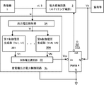
- FIG. 1 is a view schematically and schematically showing a basic configuration of a power conversion system of a rotary generator, including a first embodiment of a generator output power control circuit of the present invention.
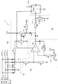
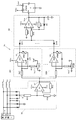
- FIG. 2 is a schematic circuit diagram including an example of the first embodiment of the generator output power control circuit.
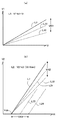
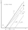
- FIGS. 3A and 3B are graphs for explaining the operation of each of the first control voltage generation unit and the second control voltage generation unit in the circuit of FIG.
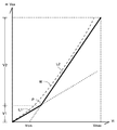
- FIG. 4 is a graph for explaining the operation of the control voltage selection unit in the circuit of FIG.
- FIG. 5 is a schematic circuit diagram showing the main part of a modification of the embodiment of FIG. 6 is a view similar to FIG. 4 in the circuit of FIG. FIG.
- FIG. 7 is a view schematically and schematically showing a basic configuration of a power conversion system of a rotary generator, including a second embodiment of a generator output power control circuit according to the present invention.
- FIG. 8 is a schematic circuit diagram including an example of the second embodiment of the generator output power control circuit.
- FIG. 9 is a graph for explaining the operation of the control voltage generation unit in the circuit of FIG.
- FIG. 10 is a graph for illustrating the operation of the control voltage selection unit in the circuit of FIG.
- FIG. 11 (a) is a schematic circuit diagram of another example of the second embodiment of the generator output power control circuit, and FIG. 11 (b) shows only a part of a plurality of resistors connected in series.
- FIG. FIG. 12 is a graph for explaining the operation of the control voltage selection unit in the circuit of FIG. 11 (a).
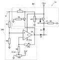
- FIG. 13 shows an example of a circuit provided at the output stage of the generator output power control circuit.
- FIG. 1 shows the power of a rotating machine generator including the first embodiment of the generator output power control circuit of the present invention.
- FIG. 1 schematically and schematically shows the basic configuration of a conversion system.
- the generator 1 is a rotating machine-type alternating current or direct current generator, for example, a wind power generator.
- the generator 1 includes a three-phase stator coil Y-connected to a rotor, for example, a permanent magnet.
- the shaft of the generator 1 is connected to the shaft of the wind turbine via appropriate gears.
- the rotational speed of the wind turbine is proportional to the wind speed, and the rotational speed of the generator 1 is proportional to the rotational speed of the wind turbine.
- a three-phase AC voltage is output from the three-phase stator coil.
- the output voltage is proportional to the number of revolutions of the generator.
- the output voltage vi of the generator represents the effective value of the phase voltage or line voltage of the three-phase alternating current or a value proportional to these.
- the present invention is also applicable to, for example, a rotary machine type generator of hydroelectric power generation other than wind power generation. Moreover, it is applicable also to the rotary machine type generator which outputs single phase alternating current and direct current
- the PWM IC 4 is configured to output, from an output terminal (out), a PWM signal vout having a duty ratio D that is proportional to the duty ratio control voltage Vcs input to the control terminal (cs).
- a PWM signal vout having a duty ratio D that is proportional to the duty ratio control voltage Vcs input to the control terminal (cs).
- a high frequency carrier triangular wave voltage and a duty ratio control voltage Vcs are input to a comparator, and an output pulse signal of the comparator is obtained as a PWM signal vout.
- the power conversion circuit 2 is configured of a switching power supply such as a power factor correction circuit (PFC) and / or a DC / DC converter. Basically, it has a configuration for performing switching control to conduct or cut off the input current Ii.
- the power conversion circuit 2 has a switching element (not shown) that is controlled to be turned on and off by the PWM signal.
- the amount of input current Ii absorbed by the power conversion circuit 2 from the generator 1 changes with the duty ratio D of the PWM signal.
- the input current Ii is an output current when viewed from the generator 1. Therefore, the output power of the generator 1 can be controlled by controlling the duty ratio D of the PWM signal according to the output voltage vi of the generator.
- the generator output power control circuit 3 has, as main functions, an output voltage detection unit 3A, a first control voltage generation unit 3B1, a second control voltage generation unit 3B2, and a control voltage selection unit 3D.
- the output voltage detection unit 3A detects the magnitude of the output voltage vi of the generator 1.
- the output voltage detection unit 3A may detect the rotation speed of the generator 1.
- the converted voltage signal can be handled equivalently to the output voltage vi of the generator 1 by converting the detected rotational speed of the generator 1 into an appropriate voltage signal proportional thereto.
- the output voltage detection unit 3A outputs a DC voltage Vi having a magnitude corresponding to the magnitude of the output voltage vi (or the number of revolutions) of the generator 1.
- the voltage Vi output from the output voltage detection unit 3A will be described by regarding it as the detected output voltage of the generator 1.
- the first control voltage generation unit 3B1 generates a first control voltage V1 based on the output voltage Vi detected by the output voltage detection unit 3A.
- the first control voltage V1 is a DC voltage that is proportional to the detected output voltage Vi via a predetermined first proportional constant k1.
- the second control voltage generation unit 3B2 generates a second control voltage V2 based on the output voltage Vi detected by the output voltage detection unit 3A. For example, in wind power generation, the generated power is generally not taken out while the wind speed is extremely low, and the generated power is taken out in earnest after exceeding a predetermined cut-in point.
- the second control voltage generation unit 3B2 does not generate the second control voltage V2 in a range in which the detected output voltage Vi is smaller than the cut-in voltage Vcin (or cut-in rotation number) corresponding to the predetermined cut-in point. It is configured.
- the second control voltage generation unit 3B2 cuts the cut-in voltage Vcin and the output voltage Vi. And a difference between the cut-in voltage Vcin and the output voltage Vi, to generate a second control voltage V2.
- the second control voltage V2 is a DC voltage proportional to an increase from the cut-in voltage Vcin to the output voltage Vi via a predetermined second proportionality constant k2.
- the second proportionality constant k2 is set larger than the first proportionality constant k1 described above (k1 ⁇ k2).
- the control voltage selection unit 3D selects one of the first control voltage V1 generated by the first control voltage generation unit 3B1 and the second control voltage V2 generated by the second control voltage generation unit 3B2. The larger voltage is selected to be selected.
- the control voltage selection unit 3D generates the duty ratio control voltage Vcs based on the selected first control voltage V1 or the second control voltage V2. The duty ratio control voltage Vcs generated in this manner is input to the control terminal (cs) of the PWM IC 4.
- the output voltage Vo of the power conversion circuit 2 is fed back to the feedback terminal (fb) of the PWM IC 4.
- the feedback line is also isolated by a photocoupler or the like.
- the output voltage Vo of the power conversion circuit 2 is controlled, for example, to maintain a constant voltage.
- FIG. 2 is a schematic circuit configuration diagram including an example of the first embodiment of the generator output power control circuit.
- the output voltage vi of the generator 1 is a three-phase alternating current.
- the output voltage detection unit 3A has a first set of three diodes whose anodes are connected to the respective phase lines R, S and T of three-phase alternating current and whose cathodes are commonly connected, and each phase line R, S, A second set of three diodes, each having its cathode connected to T and its anode connected in common to the ground point, is comprised.
- the three-phase alternating current output voltage vi is detected by full-wave rectification with these six diodes, and a direct current output voltage Vi is output between the common connection point of the first set of diodes and the ground point.
- the direct current output voltage Vi is applied to the first control voltage generator 3B1 and the second control voltage generator 3B2.
- the circuit configuration of the output voltage detection unit 3A for detecting the output voltage Vi (or the number of revolutions) of the rotary generator can be variously considered in addition to the circuit shown in FIG. In FIG. 2, three coils each having one end connected to each phase line R, S, T of three-phase alternating current are an example of the input unit of the power conversion circuit 2 shown in FIG. 1.
- a resistor R1 and a variable resistor VR1 are connected in series between the input terminal to which the output voltage Vi detected by the output voltage detection unit 3A is applied and the ground point.
- the variable resistor VR1 has an intermediate terminal.
- the output voltage Vi is divided by the resistance value obtained by adding the resistances from the resistor R1 to the intermediate terminal of the variable resistor VR1 and the resistance value from the intermediate terminal of the variable resistor VR1 to the ground point. Therefore, the potential of the intermediate terminal of the variable resistor VR1 (ie, the voltage between this intermediate terminal and the ground point) changes in proportion to the output voltage Vi.
- An npn-type transistor Q is connected to take out the potential of the intermediate terminal of the variable resistor VR1.
- the transistor Q has a collector connected to an appropriate DC power supply + Vcc, a base connected to the middle terminal of the variable resistor VR1, an emitter connected to the emitter resistor R2, and the other end of the emitter resistor R2 connected to the ground point .
- the transistor Q constitutes an emitter follower circuit, and the emitter potential thereof changes in accordance with the potential of the intermediate terminal of the variable resistor VR1. That is, the emitter potential of the transistor Q changes in proportion to the output voltage Vi.
- the proportionality factor in this proportionality relation is the first proportionality constant k1 of FIG.
- the first proportional constant k1 can be adjusted by changing the position of the intermediate terminal of the variable resistor VR1.
- the voltage between the emitter of the transistor Q and the ground is the first control voltage V1.
- the diode D3 is provided to obtain a first control voltage V1 of positive voltage.
- the circuit configuration of the first control voltage generation unit 3B1 that generates the first control voltage V1 that is proportional to the detected output voltage Vi (or the number of rotations) via the predetermined proportional constant k1 is shown in FIG. There are various possibilities other than the circuit shown.
- ⁇ Second control voltage generation unit 3B2> In the input stage of the second control voltage generation unit 3B2, the resistor R3 and the resistor R4 are connected in series between the input terminal to which the output voltage Vi detected by the output voltage detection unit 3A is applied and the ground point. The output voltage Vi is divided by the resistors R3 and R4.
- the second control voltage generation unit 3B2 has an OP amplifier A that constitutes a non-inverting amplifier.
- the OP amplifier A is supplied with power from the positive power supply + Vcc and the negative power supply -Vcc.
- the potential at the connection point of the resistors R3 and R4 ie, the voltage between this connection point and the ground point
- a variable resistor VR2 is connected between the output end of the OP amplifier A and the inverting input end ( ⁇ ).
- the variable resistor VR2 and the resistor R5 constitute a feedback circuit for amplification.
- the amplification factor is determined by 1 + VR2 / R5. Therefore, the amplification factor can be adjusted by the variable resistor VR2.
- the reference potential of the inverting input terminal (-) is the ground potential.
- a potential higher than the ground point potential is used as the reference potential.
- the reference potential is defined by the potential of the intermediate terminal of the variable resistor VR3 connected between the reference power supply Vref of appropriate size and the ground point.
- One end of the resistor R5 is not connected to the ground point, but is connected to the middle terminal of the variable resistor VR3.
- the potential of the intermediate terminal of variable resistor VR3 (ie, the voltage between this intermediate terminal and the ground point) is set to correspond to the cut-in point of generator 1, ie, the cut-in voltage Vcin (or cut-in rotational speed) .
- the potential at the intermediate terminal of the variable resistor VR3 corresponds to a value obtained by dividing the actual cut-in voltage Vcin by the resistors R3 and R4. Since the potential at the intermediate terminal of the variable resistor VR3 is not the actual cut-in voltage Vcin itself, the potential at the intermediate terminal of the variable resistor VR3 is indicated by Vcin 'in FIG.
- the setting of the cut-in voltage Vcin of the output voltage Vi can be changed by adjusting the middle terminal of the variable resistor VR3.
- the OP amplifier A does not output a positive voltage until the input voltage at the non-inverting input terminal (+) exceeds the cut-in voltage Vcin ', and the input voltage at the non-inverting input terminal (+) cuts the cut-in voltage Vcin' If it exceeds, it outputs a positive voltage amplified by amplification factor 1 + VR2 / R5. In that case, the difference between the input voltage at the non-inverting input terminal (+) and the cut-in voltage Vcin ', that is, the increase from the cut-in voltage Vcin' to the input voltage at the non-inverting input terminal (+) is amplified.
- the OP amplifier A does not output a positive voltage until the output voltage Vi exceeds the cut-in voltage Vcin.
- a positive voltage is output from the OP amplifier A.
- a voltage proportional to the increase from the cut-in voltage Vcin to the output voltage Vi at that time is output from the OP amplifier A.
- the proportionality constant in this proportionality relation is the second proportionality constant k2 of FIG.
- the second proportional constant k2 can be adjusted by adjusting the amplification factor of the OP amplifier A with the variable resistor VR2.
- the output voltage of the OP amplifier A becomes the second control voltage V2.
- the diode D4 is provided to obtain a second control voltage V2 of positive voltage.
- the circuit configuration of the second control voltage generation unit 3B2 that generates the second control voltage V2 that is proportional via the predetermined proportional constant k2 can be variously considered in addition to the circuit shown in FIG.
- the second proportional constant k2 can be set to be larger than the first proportional constant k1 (k1 ⁇ k2). , Determine the value of each relevant resistance and variable resistance.
- the control voltage selection unit 3D has a diode D1 and a diode D2 as two input terminals. One input end is the anode of the diode D1 and is connected to the emitter of the transistor Q of the first control voltage generator 3B1. Therefore, the first control voltage V1 is applied to the anode of the diode D1. The other input end is the anode of the diode D2, and is connected to the output end of the OP amplifier A of the second control voltage generation unit 3B2. Therefore, the second control voltage V2 is applied to the anode of the diode D2.
- the cathodes of the diode D1 and the diode D2 are connected in common. Therefore, at the cathode connection end of the diode D1 and the diode D2, the higher one of the potentials of the anodes of the diode D1 and the diode D2 appears. That is, the larger one of the first control voltage V1 and the second control voltage V2 is selected.
- the selected first control voltage V1 or second control voltage V2 is appropriately divided by the resistors 6 and 7.
- the divided voltage is used as the duty ratio control voltage Vcs.
- the duty ratio control voltage Vcs is a voltage proportional to the selected first control voltage V1 or the second control voltage V2.
- the resistor 7 and the capacitor C connected in parallel function as a filter for noise removal.
- the duty ratio control voltage Vcs generated in this manner is applied to the control end (cs) of the PWM IC 4.
- the circuit configuration of the control voltage generation unit 3D for selecting the voltage having the larger absolute value among the first control voltage V1 and the second control voltage V2 is not limited to the circuit shown in FIG. There are many possibilities.
- the reason why “the larger absolute value” is used is that a circuit configuration that generates the first control voltage V1 and the second control voltage V2 not as a positive voltage but as a negative voltage is also possible. In that case, since the duty ratio control voltage Vcs is usually a positive voltage, the selected negative voltage may be inverted to a positive voltage.
- the PWM IC 4 generates a PWM signal having a duty ratio corresponding to the duty ratio control voltage Vcs inputted to the control terminal (cs), and sends it to the power conversion circuit as shown in FIG.
- a switching element that is on / off controlled by the PWM signal performs switching on the output current Ii of the generator. As a result, the output power of the generator can be controlled according to the desired characteristic curve.
- FIG. 3A is a graph for explaining the operation of the first control voltage generator 3B1 in the circuit of FIG.
- the horizontal axis is the output voltage Vi
- the vertical axis is the first control voltage V1.
- the proportionality constant k1 which is the slope of the straight line L1, can be adjusted by changing the position of the intermediate terminal of the variable resistor VR1 (see the straight lines L11 and L12 shown by dotted lines).
- FIG. 3B is a graph for explaining the operation of the second control voltage generator 3B2 in the circuit of FIG.
- the horizontal axis is the output voltage Vi
- the vertical axis is the second control voltage V2.
- a straight line L2 indicates the relationship between the output voltage Vi and the second control voltage V2 when the variable resistor VR2 and the variable resistor VR3 are set to predetermined values or positions, respectively. This relationship is expressed by the following equation [2].
- V2 k2 ⁇ (Vi-Vcin) [2]
- the proportionality constant k2 which is the slope of the straight line L2, can be adjusted by changing the size of the variable resistor VR2 (see straight lines L21 and L22 indicated by dotted lines).
- the proportionality constant k2 in FIG. 3 (b) is set to be larger (k1 ⁇ k2) than the proportionality constant k1 in FIG. 3 (a). That is, the inclination of the straight line L2 is made larger than the inclination of the straight line L1.
- the cut-in voltage Vcin at which the straight line L2 intersects with the horizontal axis can be adjusted by changing the position of the intermediate terminal of the variable resistor VR3 (see straight lines L23 and L24 indicated by dotted lines).
- FIG. 4 is a graph for explaining the operation of the control voltage selection unit 3D in the circuit of FIG.
- the horizontal axis is the output voltage Vi
- the vertical axis is the duty ratio control voltage Vcs (or a voltage proportional thereto).
- the straight line L1 in FIG. 3A showing the relationship between the output voltage Vi and the first control voltage V1
- the straight line L2 in FIG. 3B showing the relationship between the output voltage Vi and the second control voltage V2. It is shown.
- a thick line indicates a locus in which the larger one of the first control voltage V1 and the second control voltage V2 is selected with respect to the same value of the output voltage Vi.
- the straight line L2 is shifted to the positive side by the cut-in voltage Vcin, and the slope k2 of the straight line L2 is larger than the slope k1 of the straight line L1, so the straight line L1 and the straight line L2 intersect at one point P.
- the first control voltage V1 is selected in a region where the output voltage Vi is smaller than the point P
- the second control voltage V2 is selected as a duty ratio control voltage Vcs in a region where the output voltage Vi is larger than the point P.
- the degree of increase of the duty ratio control voltage Vcs is moderate.
- the degree of increase of the duty ratio control voltage Vcs becomes large.
- the on period of the PWM signal can be extended to take in a large current, that is, take in a large generated output power.
- an example of a curve that can obtain the relationship between the output voltage Vi and the ideal generated power is indicated by a curve W of a dashed line.
- the generated output power control circuit according to the present invention pseudo-implements this ideal curve W with an extremely simple configuration.
- the straight lines L1 and L2 drawn by the duty ratio control voltage Vcs generated by the circuit of the present invention do not exceed the ideal curve W. This is because, when the straight lines L1 and L2 exceed the ideal curve W, the power conversion circuit takes in power excessively, and for example, in the case of wind power generation, the wind turbine is braked and decelerated.
- variable resistor VR2 is adjusted to make the slope of the straight line L2 By increasing the amount of power taken by hurrying, the generator overspeed can be suppressed easily and quickly.
- FIG. 5 schematically shows only the main part of the generator output power control circuit 3a.
- the diode D4 is removed from the circuit configuration of FIG. 2, and an npn type transistor Q2 and a resistor R8 are added.
- the transistor Q2 has a collector connected to the connection point between the resistor R1 of the first control voltage generation unit 3B1 and the variable resistor VR1, and an emitter connected to the output terminal of the OP amplifier A of the second control voltage generation unit 3B2.
- the base is grounded via a resistor R8.
- the output terminal of the OP amplifier A becomes a negative voltage
- the transistor Q2 conducts.
- the connection point between the resistor R1 of the first control voltage generation unit 3B1 and the variable resistor VR1 is substantially zero volts.
- the control voltage V1 generated by the first control voltage generator 3B1 also becomes zero volts.
- the OP amplifier A When the output voltage Vi exceeds the cut-in voltage Vcin, the OP amplifier A outputs a positive voltage, and the transistor Q2 is cut off. As a result, a divided voltage of the output voltage Vi appears at the connection point between the resistor R1 of the first control voltage generator 3B1 and the variable resistor VR1, and the first control voltage generator 3B1 generates a predetermined control voltage V1. .
- FIG. 6 is a view similar to FIG. 4 in the case of the circuit configuration of FIG. As indicated by the thick line, when the output voltage Vi is less than the cut-in voltage Vcin, the control voltage V1 is zero volts, and when the output voltage Vi reaches the cut-in voltage Vcin, the control voltage V1 is generated.
- FIG. 7 shows the power of a rotary machine type generator including a second embodiment of the generator output power control circuit of the present invention. It is the figure which showed the basic composition of the conversion system roughly and typically.
- the generator 1, the PWM IC 4 and the power conversion circuit 2 are basically the same as those in the first embodiment described above, and thus the description thereof is omitted.
- the generator output power control circuit 3b has an output voltage detection unit 3A, a plurality of control voltage generation units, and a control voltage selection unit 3D as main functions.
- the plurality of control voltage generation units basically have the same circuit configuration and are arranged in parallel in N, first to Nth control voltage generation units 3B1. . It has 3 BN (N is a natural number of 2 or more).
- the output voltage detection unit 3A detects the magnitude of the output voltage vi of the generator 1.
- the output voltage detection unit 3A may detect the rotation speed of the generator 1.
- the converted voltage signal can be handled equivalently to the output voltage vi of the generator 1 by converting the detected rotational speed of the generator 1 into an appropriate voltage signal proportional thereto.
- the output voltage detection unit 3A outputs a DC voltage Vi having a magnitude corresponding to the magnitude of the output voltage vi (or the number of revolutions) of the generator 1.
- the voltage Vi output from the output voltage detection unit 3A will be described by regarding it as the detected output voltage of the generator 1.
- the first control voltage generation unit 3B1 generates a first control voltage V1 based on the output voltage Vi detected by the output voltage detection unit 3A. For example, in wind power generation, the generated power is generally not taken out while the wind speed is extremely low, and the generated power is taken out in earnest after exceeding a predetermined cut-in point.
- the first control voltage generation unit 3B1 does not generate the first control voltage V1 in a range in which the detected output voltage Vi is smaller than the cut-in voltage Vc1 (or cut-in rotational speed) corresponding to the predetermined cut-in point. It is configured.
- the first control voltage generation unit 3B1 includes a function for setting the predetermined cut-in voltage Vc1 (or cut-in rotational speed).
- the first control voltage generation unit 3B1 when the detected output voltage Vi exceeds the cut-in voltage Vc1 (or cut-in rotational speed) corresponding to the predetermined cut-in point, the first control voltage generation unit 3B1 generates the cut-in voltage Vc1 and the output voltage Vi. difference, namely generating a first control voltage V1 based on the increase in the cut-in voltage Vc 1 to the output voltage Vi.
- the first control voltage V1 is a DC voltage proportional to an increase from the cut-in voltage Vc1 to the output voltage Vi via a predetermined proportionality constant k1.
- the first control voltage generator 3B1 includes a function to set the predetermined proportional constant k1.
- N first control voltage generation units 3B1. Each of the N-th control voltage generation units 3BN has basically the same configuration. However, control voltage generation unit 3B1. .
- a predetermined cut-in voltage Vc1 set in each of 3BN. . VcN and a predetermined proportional constant k1. . kN can be set independently.
- Control voltage selection unit 3D includes N control voltage generation units 3B1. . N control voltages V1. . The voltage with the largest absolute value is selected among VN. The control voltage selection unit 3D generates the duty ratio control voltage Vcs based on the selected control voltage. The duty ratio control voltage Vcs generated in this manner is input to the control terminal (cs) of the PWM IC 4.
- FIG. 8 is a schematic circuit configuration diagram including an example of the second embodiment of the generator output power control circuit.
- the second to the (N-1) th control voltage generators are not shown for simplification.
- N control voltage generation units 3B1. The illustration of the second to the (N-1) th elements is omitted also for the N elements provided corresponding to 3BN.
- the output voltage vi of the generator 1 is a three-phase alternating current.
- the output voltage detection unit 3A has a first set of three diodes whose anodes are connected to the respective phase lines R, S and T of three-phase alternating current and whose cathodes are commonly connected, and each phase line R, S, A second set of three diodes, each having its cathode connected to T and its anode connected in common to the ground point, is comprised.
- the three-phase AC output voltage vi is detected by full-wave rectification with these six diodes, and a DC voltage Vi is output between the common connection point of the first set of diodes and the ground point.
- the DC voltage Vi is divided by the resistors R11 and R12 connected in series.
- the potential at the connection point of the resistor R11 and the resistor R12 (ie, the voltage between this connection point and the ground point) is input to the non-inverting input terminal (+) of the OP amplifier A1 that constitutes a voltage follower (amplification factor of 1). Ru.
- the voltage output to the output terminal of the OP amplifier A1 is proportional to the DC voltage Vi.
- the OP amplifier A1 is provided to output a sufficient current to the subsequent stage.
- the resistor R13 is provided to stabilize the voltage follower.
- the OP amplifier A1 is driven by the positive power supply + Vcc and the negative power supply -Vcc (the same applies to the following OP amplifiers).
- the circuit configuration of the output voltage detection unit 3A for detecting the output voltage Vi (or the number of revolutions) of the rotary generator can be variously considered in addition to the circuit shown in FIG. In FIG. 8, three coils each having one end connected to each phase line R, S, T of three-phase alternating current are an example of the input unit of the power conversion circuit 2 shown in FIG. 7.
- the first control voltage generation unit 3B1 has an OP amplifier A21 that constitutes an inverting amplifier.
- the output voltage of the OP amplifier A1 is input to the inverting input terminal (-) of the OP amplifier A21 via the resistor R41.
- a variable resistor VRt1 is connected between the output end of the OP amplifier A21 and the inverting input end ( ⁇ ).
- the variable resistor VRt1 and the resistor R41 constitute a feedback circuit for amplification.
- the amplification factor is determined by -VRt1 / R41. Therefore, the amplification factor can be adjusted by the variable resistor VRt1. Since the diode D41 connected in series to the variable resistor VRt1 blocks the reverse current, the OP amplifier A21 outputs only a negative voltage.
- the reference potential of the non-inverting input terminal (+) is the ground potential.
- a potential higher than the ground point potential is used as the reference potential.
- the reference potential is defined by the potential of the intermediate terminal of the variable resistor VRc1 connected between the reference power supply Vref of appropriate size and the ground point.
- the non-inverted input terminal (+) is connected to the middle terminal of the variable resistor VRc1 instead of the ground point via the resistor R51.
- the potential of the intermediate terminal of variable resistor VRc1 (that is, the voltage between this intermediate terminal and the ground point) is set to correspond to the cut-in point of generator 1, that is, cut-in voltage Vc1 (or cut-in rotational speed) .
- the potential at the intermediate terminal of the variable resistor VRc1 corresponds to a value obtained by dividing the actual cut-in voltage Vc1 by the resistors R11 and R12. Therefore, since the potential at the intermediate terminal of the variable resistor VRc1 is not the actual cut-in voltage Vc1 itself, in FIG. 8, the potential at the intermediate terminal of the variable resistor VRc1 is indicated by Vc1 '.
- the setting of the cut-in voltage Vc1 of the output voltage Vi can be changed by adjusting the middle terminal of the variable resistor VRc1.
- the OP amplifier A21 has an output voltage of zero volts until the input voltage Vi 'to the input end of the resistor R41 exceeds the cut-in voltage Vc1'.
- the input voltage Vi ′ exceeds the cut-in voltage Vc1 ′, it outputs a negative voltage amplified by the amplification factor ⁇ VRt 1 / R41.
- the difference between the input voltage Vi ′ and the cut-in voltage Vc1 ′ that is, the increase from the cut-in voltage Vc1 ′ to the input voltage Vi ′ is amplified.
- the actual output voltage Vi will be described.
- the voltage is not output from the OP amplifier A21 until the output voltage Vi exceeds the cut-in voltage Vc1.
- a negative voltage is output from the OP amplifier A21.
- a voltage V1 proportional to an increase from the cut-in voltage Vc1 to the output voltage Vi is output from the OP amplifier A21.
- the proportionality constant in this proportionality relation is the proportionality constant k1 of FIG.
- the proportional constant k1 can be adjusted by adjusting the amplification factor of the OP amplifier A21 with the variable resistor VRt1.
- the output voltage V1 of the OP amplifier A21 is the first control voltage generated by the first control voltage generator 3B1.
- the circuit configuration of the first control voltage generation unit 3B1 that generates the first control voltage V1 proportional to the absolute value through the predetermined proportional constant k1 can be variously considered in addition to the circuit shown in FIG. Although this embodiment is configured with an inverting amplifier, it may be configured with a non-inverting amplifier (see, for example, the first embodiment).
- N control voltage generation units 3B1. The circuit configuration of each of 3BN is basically the same, but the variable resistor VRt1. . Each value of VRtN, variable resistor VRc1. . The value of each of VRcN, the value of the other resistance, etc. can be different.
- the control voltage selection unit 3D has N diodes D11. . It has D1N. N diodes D11. . Each of D1N has its cathode at N control voltage generation units 3B1. . Each 3 OP op amp A21. . It is connected to the output of A2N. Therefore, the diode D11. . The first to Nth control voltages V1. . Each of VN is applied respectively.
- the anodes of D1N are commonly connected. Therefore, the diode D11. .
- the lowest potential of the cathode potential of each of D1N appears. In other words, only the diode with the lowest cathode potential is forward biased and conducts. That is, the first to Nth control voltages V1. .
- the largest voltage appears in absolute value. Thereby, the first to Nth control voltages V1. .
- the control voltage with the largest absolute value is selected.
- the selected control voltage is inverted and amplified by the OP amplifier A3 constituting the inverting amplifier.
- the amplification factor is determined by -R17 / R16 by the resistors R16 and R17.
- the OP amplifier A3 outputs a positive voltage.
- the voltage at the output terminal of the OP amplifier A3 is used as the duty ratio control voltage Vcs.
- the duty ratio control voltage Vcs is a voltage proportional to the selected control voltage.
- the capacitor C is for smoothing, and the zener diode ZD is for output voltage limitation.
- the duty ratio control voltage Vcs generated in this manner is applied to the control end (cs) of the PWM IC 4.
- the first to Nth control voltages V1. The circuit configuration of the control voltage generation unit 3D for selecting the control voltage having the largest absolute value in VN can be variously considered other than the circuit shown in FIG.
- the PWM IC 4 generates a PWM signal having a duty ratio corresponding to the duty ratio control voltage Vcs inputted to the control terminal (cs), and sends it to the power conversion circuit as shown in FIG.
- a switching element that is on / off controlled by the PWM signal performs switching on the output current Ii of the generator. As a result, the output power of the generator can be controlled according to the desired characteristic curve.
- FIG. 9 is a graph for explaining the operation of the first control voltage generator 3B1 in the circuit of FIG.
- the horizontal axis of the output voltage Vi, the vertical axis represents the first absolute value of the control voltage V 1.
- Straight line L1 shows the variable resistor VRt1 and the variable resistor Vrc1 1 each when set to a predetermined size or position, the relationship between the absolute value of the output voltage Vi and the first control voltage V1. This relationship is expressed by the following equation.
- k1 ⁇ (Vi ⁇ Vc1)
- the proportionality constant k1, which is the slope of the straight line L1, can be adjusted by changing the magnitude of the variable resistor VRt1 (see the straight lines L11 and L12 indicated by dotted lines).
- the cut-in voltage Vc1 at which the straight line L1 intersects the horizontal axis can be adjusted by changing the position of the intermediate terminal of the variable resistor VRc1 (see straight lines L13 and L14 indicated by dotted lines).
- FIG. 10 is a graph for explaining the operation of the control voltage selection unit 3D in the circuit of FIG.
- N 3.
- the horizontal axis is the output voltage Vi
- the vertical axis is the duty ratio control voltage Vcs (or a voltage proportional thereto).
- a straight line L1, a straight line L2, and a straight line L3 indicating the relationship between the output voltage Vi and the first control voltage V1, the second control voltage V2, and the third control voltage V3 are shown by dotted lines.
- the intersections with the horizontal axes of the respective straight lines correspond to the set cut-in voltages Vc1, Vc2, and Vc3.
- the inclination of each straight line is also set to a predetermined value.
- a thick line indicates a locus in which the control voltage having the largest absolute value is selected for the same value of the output voltage Vi.
- the straight line L1 and the straight line L2 intersect at a point Pa, and the straight line L2 and the straight line L3 intersect at a point Pb.
- the point Pa and the point Pb are turning points at which one straight line is shifted to the other straight line.
- the first control voltage V1 is selected in a region where the output voltage Vi is small, the second control voltage V2 in a middle region, and the third control voltage V3 in a large region as the duty ratio control voltage Vcs.
- the conditions under which such a transition point is formed are as follows. Vc1 ⁇ Vc2 ⁇ Vc3, and k1 ⁇ k2 ⁇ k3
- the duty ratio control voltage Vcs is zero volts. That is, no power is taken from the generator.
- the output voltage Vi exceeds the cut-in voltage Vc 1
- the duty ratio control voltage Vcs according straight line L1 is generated, the slope is gradual.
- duty ratio control voltage Vcs is generated according to straight line L2 having a larger inclination than straight line L1
- duty ratio control voltage is generated according to straight line L3 having a larger inclination than straight line L2.
- Vcs is generated.
- the relationship between the output voltage Vi and the ideal generated power can be obtained by a curve W of a dashed line.
- the duty ratio control voltage Vcs along the ideal curve W usually, in order to generate the duty ratio control voltage Vcs along the ideal curve W, complicated circuits and programs are required.
- the generated output power control circuit according to the present invention pseudo-implements this ideal curve W with an extremely simple configuration.
- the straight lines L1, L2, and L3 drawn by the duty ratio control voltage Vcs generated by the circuit of the present invention do not exceed the ideal curve W. This is because, for example, in the case of wind power generation, the wind turbine is braked and decelerates because the power conversion circuit takes in excess power when the straight lines L1, L2, L3 exceed the ideal curve W. .
- the control voltage generation unit selected at that time By adjusting the variable resistance VRt3 of 3B3 to make the inclination of the straight line L3 steep to increase the amount of power taken in, it is possible to suppress the over-rotation of the generator easily and quickly.
- FIG. 11A is a schematic circuit configuration diagram of another example of the second embodiment of the generator output power control circuit.
- FIG. 11 (b) shows only a part of the circuit of (a).
- each of the output voltage detection unit 3A, the first control voltage generation unit 3B1, the Nth control voltage generation unit 3BN, and the control voltage selection unit 3D shown in FIG. Portions substantially corresponding to are each surrounded by a dotted line.
- the third to the (N-1) th control voltage generators are not shown for the sake of simplicity.
- the illustration of the third to the (N-1) th elements is omitted also for the N elements provided corresponding to 3BN.
- the output voltage detection unit 3A shows only a portion behind the DC voltage Vi obtained by full-wave rectification of the three-phase AC output voltage shown in FIG. In the circuit example of FIG. 11A, this DC voltage Vi is applied to the resistor R11 and the variable resistor VR12 connected in series, and the middle terminal of the variable resistor VR12 is input to the non-inverting input terminal (+) of the OP amplifier A1. doing.
- the voltage division ratio of the DC voltage Vi is fixed. However, in the circuit of FIG. 11A, the voltage division ratio can be adjusted according to the maximum voltage of the output voltage Vi. Thus, the fluctuation range of the input voltage to the OP amplifier A1 can be set to be the same regardless of the maximum voltage of the output voltage Vi.
- the OP amplifier A1 is a voltage follower. The output voltage of the OP amplifier A1 is denoted by Vi 'as in the circuit of FIG.
- the first control voltage generation unit 3B1 includes an OP amplifier A21 configured as an inverting amplifier as in the circuit of FIG.
- the output voltage of the OP amplifier A1 is input to the inverting input terminal (-) of the OP amplifier A21 via the resistor R41.
- the variable resistor VRt1 and the light emitting diode D11 are connected in series between the output end of the OP amplifier A21 and the inverting input end ( ⁇ ).
- the diode 41 in the circuit of FIG. 8 is replaced with a light emitting diode D11.
- the amplification factor of the OP amplifier A21 can be adjusted by the variable resistor VRt1.
- the light emitting diode D11 in the circuit of FIG. 11A also serves as the diode in the control voltage selection unit 3D (the diode D11 in the circuit of FIG. 8). Therefore, in the circuit of FIG. 11A, the configuration is simplified.
- the circuit of FIG. 11 (a) differs from the circuit of FIG. Here, as shown in FIG. 11 (b), N resistors Rc1, Rc2. . RcN is connected in series, and one end of RcN is further connected to a positive power supply + Vcc via a terminal resistor Re. Thereby, the N resistors Rc1 and Rc2. . A predetermined DC voltage is applied across RcN.
- the non-inverting input terminal (+) of the OP amplifier A21 of the first control voltage generation unit 3B1 is connected to one end (a connection point with the resistor Rc2) on the high potential side of the resistor Rc1 via the resistor R51.
- the potential at this point is the potential Vc1 'corresponding to the actual cut-in voltage Vc1.
- the non-inverting input terminal (+) of the OP amplifier A2N of the Nth control voltage generation unit 3BN is connected to one end (a connection point with the resistor Re) of the high potential side of the resistor RcN via the resistor R5N. There is. The potential at this point is the potential VcN 'corresponding to the actual cut-in voltage VcN.
- the non-inverting input terminals of the respective OP amplifiers in the second to (N-1) th control voltage generation units are also connected in order to one end on the high potential side of the corresponding resistance.
- the cut-in voltage of the first control voltage generation unit 3B1 is set to zero volts (similar to the first embodiment) .
- each control voltage generation unit is the same as the circuit of FIG. 8 except that the cut-in voltage of each control voltage generation unit is fixed.
- the OP amplifiers A21 to A2N constituting the inverting amplifier have an output voltage of zero volts until the input voltage Vi 'exceeds the set cut-in voltage (for example, Vc1'), and the input voltage Vi 'is a cut-in voltage. When it exceeds, it outputs a negative voltage amplified at a predetermined amplification factor. In that case, an increase from the cut-in voltage to the input voltage Vi 'is amplified.
- Control voltage selection unit 3D The control voltage selector 3D in the circuit of FIG. 11 (a) has N light emitting diodes D11. . It has D1N. Light emitting diode D11. . The common anode connection end of D1N is connected to the inverting input end (-) of the OP amplifier A3 via a resistor and connected to the positive power supply + Vcc via a constant current diode CD in order to make the diode current constant. ing.
- D1N The function of D1N is the same as that of the N diodes D11. . Same as D1N. Therefore, the light emitting diode D11. .
- the lowest of the respective cathode potentials appears at the common anode connection end of D1N. That is, the first to Nth control voltages V1. . Among VN, the largest voltage appears in absolute value. Thereby, the first to Nth control voltages V1. . Among VN, the control voltage with the largest absolute value is selected. Then, only the light emitting diode corresponding to the selected control voltage is forward biased and emits light, whereby the rotational state of the generator can be easily visually observed.
- the OP amplifier A3 constituting the inverting amplifier is similar to the circuit of FIG.
- the voltage at the output terminal of the OP amplifier A3 is used as the duty ratio control voltage Vcs.
- the upper limit of the absolute value of the control voltage V3 corresponding to the maximum output Vmax of the generator can be adjusted by the variable resistor VR12. Even when adjustment is made to the maximum output Vmax, the locus of the control voltage Vcs indicated by a thick line changes in a similar manner, and the shape along the ideal curve W can be maintained.
- the other points are as described in FIG.
- each of the N control voltage generation units has basically the same circuit configuration. However, it is not essential that the control voltage generation units have the same circuit configuration. In principle, each control voltage generation unit generates a predetermined proportional constant for an increase from the set cut-in voltage or cut-in rotation speed to the output voltage or rotation speed detected by the output voltage detection unit. A function to generate a proportional control voltage may be provided. Therefore, an embodiment in which each of the N control voltage generation units has a different circuit configuration is also included in the present invention.
- each of the N control voltage generation units has a first variable resistor for adjusting a proportional constant, and a second variable resistor for adjusting a cut-in point.
- a normal one having a constant resistance value respectively A resistor may be used.
- the cut-in point and the slope of the control voltage generated by the control voltage generation unit are fixed to one set value.
- straight line L2 in the graph of FIG. 10 is fixed and straight line L1 and straight line Only L3 is variable.
- FIG. 13 shows an example of a circuit provided in the output stage of the generator output power control circuit.
- the circuit of FIG. 13 has three PWMICs 4r, 4s, 4t to control a three-phase power conversion circuit (not shown).
- Three photocouplers PC1, PC2 and PC3 are disposed between the generator output power control circuit and the three PWMICs, and the generator output power control circuit and the PWMIC are isolated from each other.
- the light emitting diodes on the input side of the photocouplers PC1, PC2 and PC3 are connected in series.
- the control voltage Vcs output from the generator output power control circuit is applied to the anode of the light emitting diode of the photocoupler PC1, and the cathode of the light emitting diode of the photocoupler PC3 is grounded.
- the phototransistor on the output side of each of the photocouplers PC1, PC2, PC3 is connected to the PWMIC 4r, 4s, 4t via a general additional circuit, respectively.
- Each output terminal of PWMIC 4r, 4s, 4t outputs a PWM signal having a duty ratio corresponding to control voltage Vcs, to switching elements Qr, Qs, Qt in each of the three-phase power conversion circuits.
Landscapes
- Engineering & Computer Science (AREA)
- Power Engineering (AREA)
- Life Sciences & Earth Sciences (AREA)
- Sustainable Development (AREA)
- Sustainable Energy (AREA)
- Physics & Mathematics (AREA)
- Electromagnetism (AREA)
- General Physics & Mathematics (AREA)
- Radar, Positioning & Navigation (AREA)
- Automation & Control Theory (AREA)
- Control Of Eletrric Generators (AREA)
Abstract
回転機型発電機の出力電力を、発電機の出力電圧又は回転数に応じて容易にかつ迅速に制御することができる簡易な構成の発電機出力電力制御回路を提供する。 PWMICに与えるデューティ比制御電圧を生成する発電機出力電力制御回路が、出力電圧又は回転数を検知する出力電圧検知部と、所定のカットイン点に対応するカットイン電圧又はカットイン回転数から、前記出力電圧検知部により検知された前記出力電圧又は回転数までの増加分に対し、所定の比例定数を介して比例する制御電圧をそれぞれ生成する複数の制御電圧生成部と、前記複数の制御電圧生成部によりそれぞれ生成された複数の制御電圧のうち絶対値が最も大きい電圧が選択されるように構成された制御電圧選択部と、を有し、前記制御電圧選択部により選択された前記制御電圧を基にデューティ比制御電圧を生成する。
Description
本発明は、風力発電や水力発電等における回転機型発電機の出力電力を制御するための出力電力制御回路に関する。
発電機出力である交流は、電力変換回路を介して直流に変換される。電力変換回路は、力率改善回路(PFC)及び/又はDC/DCコンバータ等のスイッチング電源で構成される(特許文献1~5)。特許文献4、5には、風力発電の回転機型発電機の三相交流出力に対して昇圧と力率改善を行う装置が記載されている。
電力変換回路を構成するスイッチング電源のスイッチング制御には、一般的にPWM信号が用いられる。PWM信号のデューティ比を制御することにより、発電機から電力変換回路に入力する入力電流(発電機から視ると出力電流)の量を制御することができ、それにより発電機出力電力を制御することができる。
PWM信号の生成には、PWMICが広く用いられている。一般的なPWMICは、デューティ比制御電圧が入力される制御端子とPWM信号を出力する出力端子とを少なくとも具備する。PWM信号のデューティ比は、制御端子に入力されるデューティ比制御電圧に比例するように構成されている。
発電機出力電力の最適な制御は、発電機の出力電圧又は回転数に対して適切な発電機出力電流を設定することによって可能となる。よって、発電機の出力電圧又は回転数を検知し、それに基づいてPWMICの制御端子に入力するデューティ比制御電圧を制御することにより、PWM信号のデューティ比を制御でき、その結果、発電機出力電力を制御することが可能となる。
風力発電では、発電電圧は風速に比例し、発電電力は風速の三乗に比例するため、出力電圧の三乗に比例して発電電力を取り出すようにPWMICを制御することにより、効率的に発電電力を出力することができる。このためにPWMICを制御する制御方式として、テーブル方式やMPPT(最大電力点追従)方式が用いられているが、風況が激しく変化する小型風力発電では応答速度が遅いために追従できない問題や、プログラミングが複雑であるという問題があった。
以上の問題点に鑑み本発明は、回転機型発電機の出力電力を、発電機の出力電圧又は回転数に応じて容易にかつ迅速に制御することができる簡易な構成の発電機出力電力制御回路を提供することを目的とする。
上記の目的を達成するべく、本発明は、以下の構成を提供する。
・ 本発明の態様は、回転機型発電機の出力電流に対するスイッチング制御に用いるPWM信号のデューティ比を制御することにより該発電機の出力電力を制御するために、該PWM信号を生成するPWMICに与えるデューティ比制御電圧を生成する発電機出力電力制御回路において、
回転機型発電機の出力電圧又は回転数を検知する出力電圧検知部と、
所定のカットイン点に対応するカットイン電圧又はカットイン回転数から、前記出力電圧検知部により検知された前記出力電圧又は回転数までの増加分に対し、所定の比例定数を介して比例する制御電圧をそれぞれ生成する複数の制御電圧生成部と、
前記複数の制御電圧生成部によりそれぞれ生成された複数の制御電圧のうち絶対値が最も大きい制御電圧が選択されるように構成された制御電圧選択部と、を有し、
前記制御電圧選択部により選択された前記制御電圧を基にデューティ比制御電圧を生成することを特徴とする。
・ 上記態様において、前記複数の制御電圧生成部の各々又は一部が、前記比例定数の大きさを調整するための第1の可変抵抗を有することが、好適である。
・ 上記態様において、前記複数の制御電圧生成部の各々又は一部が、前記カットイン電圧又はカットイン回転数を調整するための第2の可変抵抗を有することが、好適である。
・ 上記態様において、前記複数の制御電圧生成部の各々が、両端に直流電圧を印加される直列接続された複数の抵抗の各々の一端における電位により、それぞれ前記カットイン電圧又はカットイン回転数を設定されることが、好適である。
・ 上記態様において、前記回転機型発電機が風力発電又は水力発電の発電機であることを特徴とする。
・ 本発明の態様は、回転機型発電機の出力電流に対するスイッチング制御に用いるPWM信号のデューティ比を制御することにより該発電機の出力電力を制御するために、該PWM信号を生成するPWMICに与えるデューティ比制御電圧を生成する発電機出力電力制御回路において、
回転機型発電機の出力電圧又は回転数を検知する出力電圧検知部と、
所定のカットイン点に対応するカットイン電圧又はカットイン回転数から、前記出力電圧検知部により検知された前記出力電圧又は回転数までの増加分に対し、所定の比例定数を介して比例する制御電圧をそれぞれ生成する複数の制御電圧生成部と、
前記複数の制御電圧生成部によりそれぞれ生成された複数の制御電圧のうち絶対値が最も大きい制御電圧が選択されるように構成された制御電圧選択部と、を有し、
前記制御電圧選択部により選択された前記制御電圧を基にデューティ比制御電圧を生成することを特徴とする。
・ 上記態様において、前記複数の制御電圧生成部の各々又は一部が、前記比例定数の大きさを調整するための第1の可変抵抗を有することが、好適である。
・ 上記態様において、前記複数の制御電圧生成部の各々又は一部が、前記カットイン電圧又はカットイン回転数を調整するための第2の可変抵抗を有することが、好適である。
・ 上記態様において、前記複数の制御電圧生成部の各々が、両端に直流電圧を印加される直列接続された複数の抵抗の各々の一端における電位により、それぞれ前記カットイン電圧又はカットイン回転数を設定されることが、好適である。
・ 上記態様において、前記回転機型発電機が風力発電又は水力発電の発電機であることを特徴とする。
本発明によれば、回転機型発電機の出力電圧又は回転数に応じて、PWMICに与えるデューティ比制御電圧を簡易な構成により容易にかつ迅速に生成することができる。従って、PWMICによりスイッチング制御される電力変換回路に入力される発電機出力電力を容易にかつ迅速に制御することを実現できる。
以下、図面を参照しつつ、本発明による、回転機型発電機の発電機出力電力制御回路の実施形態について説明する。
(1)第1の実施形態
(1-1)第1の実施形態の基本構成
図1は、本発明の発電機出力電力制御回路の第1の実施形態を含む、回転機型発電機の電力変換システムの基本的構成を概略的かつ模式的に示した図である。
(1-1)第1の実施形態の基本構成
図1は、本発明の発電機出力電力制御回路の第1の実施形態を含む、回転機型発電機の電力変換システムの基本的構成を概略的かつ模式的に示した図である。
発電機1は、回転機型の交流又は直流の発電機であり、例えば風力発電の発電機である。発電機1は、例えば永久磁石であるロータとY結線された三相のステータコイルを備えている。発電機1の軸は風車の軸と適宜のギアを介して連結されている。風車の回転数は風速に比例し、発電機1の回転数は風車の回転数に比例する。発電機1の軸が回転すると、三相のステータコイルから三相交流電圧が出力される。出力電圧は、発電機の回転数に比例する。ここでは、発電機の出力電圧viは、三相交流の相電圧若しくは線間電圧の実効値又はこれらに比例する値を表している。なお、本発明は、風力発電以外の、例えば水力発電の回転機型発電機にも適用できる。また、単相交流や直流を出力する回転機型発電機にも適用できる。
PWMIC4は、制御端子(cs)に入力されたデューティ比制御電圧Vcsに比例するデューティ比DをもつPWM信号voutを出力端子(out)から出力するように構成されている。例えば、一般的な三角波比較方式では、高周波搬送三角波電圧とデューティ比制御電圧Vcsを比較器に入力し、比較器の出力パルス信号をPWM信号voutとして得る。PWM信号voutは、数kHz~数百kHzの高周波のパルス信号であり、一周期をTとし、オン期間をTonとすると、デューティ比Dは、D=Ton/Tで表される。デューティ比制御電圧Vcsとデューティ比Dが比例することから、デューティ比制御電圧Vcsを変化させることにより、デューティ比Dを変化させることができる。
電力変換回路2は、力率改善回路(PFC)及び/又はDC/DCコンバータ等のスイッチング電源により構成されている。基本的に、入力電流Iiを導通又は遮断するスイッチング制御を行う構成を備えている。このために、電力変換回路2は、PWM信号によりオンオフ制御されるスイッチング素子(図示せず)を有する。電力変換回路2が発電機1から吸い込む入力電流Iiの量は、PWM信号のデューティ比Dによって変化する。入力電流Iiは、発電機1から視ると出力電流である。よって、発電機の出力電圧viに応じてPWM信号のデューティ比Dを制御することにより、発電機1の出力電力を制御することができる。
発電機出力電力制御回路3は、主な機能として、出力電圧検知部3Aと、第1制御電圧生成部3B1と、第2制御電圧生成部3B2と、制御電圧選択部3Dとを有する。
出力電圧検知部3Aは、発電機1の出力電圧viの大きさを検知する。なお、発電機1の出力電圧viは発電機1の回転数に比例するので、出力電圧検知部3Aは、発電機1の回転数を検知してもよい。その場合、検知した発電機1の回転数を、それに比例する適宜の電圧信号に変換することにより、その変換された電圧信号を発電機1の出力電圧viと同等に取り扱うことができる。出力電圧検知部3Aは、発電機1の出力電圧vi(又は回転数)の大きさに対応する大きさをもつ直流電圧Viを出力する。以下、出力電圧検知部3Aから出力される電圧Viを、発電機1の検知された出力電圧とみなして説明する。
第1制御電圧生成部3B1は、出力電圧検知部3Aにより検知された出力電圧Viを基に第1の制御電圧V1を生成する。第1の制御電圧V1は、検知された出力電圧Viに対し、所定の第1の比例定数k1を介して比例する直流電圧である。
第2制御電圧生成部3B2は、出力電圧検知部3Aにより検知された出力電圧Viを基に第2の制御電圧V2を生成する。例えば風力発電においては、通常、風速が極めて小さい間は発電電力の取り出しをほとんど行わず、所定のカットイン点を超えてから本格的に発電電力の取り出しを行う。第2制御電圧生成部3B2は、検知された出力電圧Viが所定のカットイン点に対応するカットイン電圧Vcin(又はカットイン回転数)より小さい範囲では第2の制御電圧V2を生成しないように構成されている。
そして、第2制御電圧生成部3B2は、検知された出力電圧Viが所定のカットイン点に対応するカットイン電圧Vcin(又はカットイン回転数)を超えると、そのカットイン電圧Vcinと出力電圧Viとの差、すなわちカットイン電圧Vcinから出力電圧Viまでの増加分を基に第2の制御電圧V2を生成する。第2の制御電圧V2は、カットイン電圧Vcinから出力電圧Viまでの増加分に対し、所定の第2の比例定数k2を介して比例する直流電圧である。ここで、第2の比例定数k2は、上述した第1の比例定数k1より大きく設定する(k1<k2)。
制御電圧選択部3Dは、第1制御電圧生成部3B1により生成された第1の制御電圧V1と、第2制御電圧生成部3B2により生成された第2の制御電圧V2のうち、いずれか絶対値の大きい方の電圧が選択されるように構成されている。制御電圧選択部3Dは、選択された第1の制御電圧V1又は第2の制御電圧V2を基にデューティ比制御電圧Vcsを生成する。このようにして生成されたデューティ比制御電圧Vcsが、PWMIC4の制御端子(cs)に入力される。
なお、電力変換回路2の出力電圧Voは、PWMIC4のフィードバック端子(fb)にフィードバックされる。電力変換回路2が絶縁型の場合は、フィードバックラインもフォトカプラ等により絶縁される。電力変換回路2の出力電圧Voは、例えば一定電圧を維持するように制御される。
(1-2)第1の実施形態の実施例の回路構成
図2は、発電機出力電力制御回路の第1の実施形態の一実施例を含む概略的な回路構成図である。図2の回路では、図1に示した出力電圧検知部3A、第1制御電圧生成3B1、第2制御電圧生成部3B2及び制御電圧選択部3Dの各々にほぼ相当する部分を、それぞれ点線で囲んで示している。
図2は、発電機出力電力制御回路の第1の実施形態の一実施例を含む概略的な回路構成図である。図2の回路では、図1に示した出力電圧検知部3A、第1制御電圧生成3B1、第2制御電圧生成部3B2及び制御電圧選択部3Dの各々にほぼ相当する部分を、それぞれ点線で囲んで示している。
<出力電圧検知部3A>
本例では、発電機1の出力電圧viは三相交流である。出力電圧検知部3Aは、三相交流の各相線R、S、Tにそれぞれアノードが接続されかつカソードが共通接続された3つのダイオードからなる第1の組と、各相線R、S、Tにそれぞれカソードが接続されかつアノードが接地点に共通接続された3つのダイオードからなる第2の組により構成されている。三相交流の出力電圧viはこれらの6つのダイオードにより全波整流されることによって検知され、第1の組のダイオードの共通接続点と接地点の間に直流の出力電圧Viが出力される。この直流の出力電圧Viは、第1制御電圧生成部3B1及び第2制御電圧生成部3B2へそれぞれ与えられる。
本例では、発電機1の出力電圧viは三相交流である。出力電圧検知部3Aは、三相交流の各相線R、S、Tにそれぞれアノードが接続されかつカソードが共通接続された3つのダイオードからなる第1の組と、各相線R、S、Tにそれぞれカソードが接続されかつアノードが接地点に共通接続された3つのダイオードからなる第2の組により構成されている。三相交流の出力電圧viはこれらの6つのダイオードにより全波整流されることによって検知され、第1の組のダイオードの共通接続点と接地点の間に直流の出力電圧Viが出力される。この直流の出力電圧Viは、第1制御電圧生成部3B1及び第2制御電圧生成部3B2へそれぞれ与えられる。
なお、回転機型発電機の出力電圧Vi(又は回転数)を検知する出力電圧検知部3Aの回路構成は、図2に示した回路以外にも多様に考えられる。図2において、三相交流の各相線R、S、Tにそれぞれ一端が接続されている3つのコイルは、図1に示した電力変換回路2の入力部の一例である。
<第1制御電圧生成部3B1>
第1制御電圧生成部3B1の入力段は、出力電圧検知部3Aにより検知された出力電圧Viが印加される入力端と接地点との間に、抵抗R1と可変抵抗VR1が直列接続されている。可変抵抗VR1は中間端子を有する。出力電圧Viは、抵抗R1と可変抵抗VR1の中間端子までの抵抗を加算した抵抗値と、可変抵抗VR1の中間端子から接地点までの抵抗値とにより分圧される。従って、可変抵抗VR1の中間端子の電位(すなわちこの中間端子と接地点との間の電圧)は、出力電圧Viに比例して変化する。
第1制御電圧生成部3B1の入力段は、出力電圧検知部3Aにより検知された出力電圧Viが印加される入力端と接地点との間に、抵抗R1と可変抵抗VR1が直列接続されている。可変抵抗VR1は中間端子を有する。出力電圧Viは、抵抗R1と可変抵抗VR1の中間端子までの抵抗を加算した抵抗値と、可変抵抗VR1の中間端子から接地点までの抵抗値とにより分圧される。従って、可変抵抗VR1の中間端子の電位(すなわちこの中間端子と接地点との間の電圧)は、出力電圧Viに比例して変化する。
可変抵抗VR1の中間端子の電位を取り出すためにnpn型のトランジスタQが接続されている。トランジスタQは、コレクタが適宜の直流電源+Vccに接続され、ベースが可変抵抗VR1の中間端子に接続され、エミッタがエミッタ抵抗R2に接続され、エミッタ抵抗R2の他端は接地点に接続されている。トランジスタQは、エミッタフォロワ回路を構成しており、そのエミッタ電位は、可変抵抗VR1の中間端子の電位に従って変化する。すなわち、出力電圧Viに比例してトランジスタQのエミッタ電位が変化する。この比例関係における比例係数が、図1の第1の比例定数k1である。第1の比例定数k1は、可変抵抗VR1の中間端子の位置を変えることにより調整可能である。トランジスタQのエミッタと接地点の間の電圧が、第1の制御電圧V1となる。ダイオードD3は、正電圧の第1の制御電圧V1を得るために設けている。
なお、検知された出力電圧Vi(又は回転数)に対し、所定の比例定数k1を介して比例する第1の制御電圧V1を生成する第1制御電圧生成部3B1の回路構成は、図2に示した回路以外にも多様に考えられる。
<第2制御電圧生成部3B2>
第2制御電圧生成部3B2の入力段は、出力電圧検知部3Aにより検知された出力電圧Viが印加される入力端と接地点との間に、抵抗R3と抵抗R4が直列接続されている。出力電圧Viは、抵抗R3と抵抗R4により分圧される。
第2制御電圧生成部3B2の入力段は、出力電圧検知部3Aにより検知された出力電圧Viが印加される入力端と接地点との間に、抵抗R3と抵抗R4が直列接続されている。出力電圧Viは、抵抗R3と抵抗R4により分圧される。
第2制御電圧生成部3B2は、非反転増幅器を構成するOPアンプAを有する。図示の例では、OPアンプAは正電源+Vccと負電源-Vccから電源供給されている。抵抗R3と抵抗R4の接続点の電位(すなわちこの接続点と接地点の間の電圧)は、非反転入力端(+)に入力される。OPアンプAの出力端と反転入力端(-)の間に可変抵抗VR2が接続されている。可変抵抗VR2と抵抗R5が、増幅作用のための帰還回路を構成する。増幅率は、1+VR2/R5で決定される。従って、増幅率は可変抵抗VR2により調整可能である。
通常の非反転増幅器の場合、反転入力端(-)の基準電位は接地点電位である。しかしながら、本回路では、接地点電位よりも高い電位を基準電位としている。基準電位は、適宜の大きさの参照電源Vrefと接地点の間に接続された可変抵抗VR3の中間端子の電位により規定される。抵抗R5の一端は、接地点ではなく、可変抵抗VR3の中間端子に接続されている。
可変抵抗VR3の中間端子の電位(すなわちこの中間端子と接地点の間の電圧)は、発電機1のカットイン点すなわちカットイン電圧Vcin(又はカットイン回転数)に対応するように設定される。可変抵抗VR3の中間端子の電位は、実際のカットイン電圧Vcinを抵抗R3と抵抗R4で分圧した値に相当する。可変抵抗VR3の中間端子の電位は、実際のカットイン電圧Vcinそのものではないので、図2では、可変抵抗VR3の中間端子の電位をVcin’で示している。可変抵抗VR3の中間端子を調整することにより、出力電圧Viのカットイン電圧Vcinの設定を変えることができる。
OPアンプAは、非反転入力端(+)の入力電圧がカットイン電圧Vcin’を超えるまでは正の電圧を出力せず、非反転入力端(+)の入力電圧がカットイン電圧Vcin’を超えると、増幅率1+VR2/R5で増幅された正の電圧を出力する。その場合、非反転入力端(+)の入力電圧とカットイン電圧Vcin’との差、すなわちカットイン電圧Vcin’から非反転入力端(+)の入力電圧までの増加分が増幅される。
実際の出力電圧Viに関して説明する。出力電圧Viがカットイン電圧Vcinを超えるまでは、OPアンプAから正の電圧が出力されない。出力電圧Viがカットイン電圧Vcinを超えると、OPアンプAから正の電圧が出力されるようになる。その場合、カットイン電圧Vcinからそのときの出力電圧Viまでの増加分に比例する電圧がOPアンプAから出力される。この比例関係における比例定数が、図1の第2の比例定数k2である。第2の比例定数k2は、可変抵抗VR2によりOPアンプAの増幅率を調整することにより調整可能である。OPアンプAの出力電圧が、第2の制御電圧V2となる。ダイオードD4は、正電圧の第2の制御電圧V2を得るために設けている。
なお、検知された出力電圧Vi(又は回転数)に対し、所定のカットイン点に対応するカットイン電圧(又はカットイン回転数)から出力電圧Vi(又は回転数)までの増加分に対し、所定の比例定数k2を介して比例する第2の制御電圧V2を生成する第2制御電圧生成部3B2の回路構成は、図2に示した回路以外にも多様に考えられる。
また、第1制御電圧生成部3B1及び第2制御電圧生成部3B2の回路設計においては、第2の比例定数k2を第1の比例定数k1よりも大きく(k1<k2)設定可能であるように、関係する各抵抗及び可変抵抗の値を決定する。
<制御電圧選択部3D>
制御電圧選択部3Dは、2つの入力端としてダイオードD1とダイオードD2を有する。一方の入力端は、ダイオードD1のアノードであり、第1制御電圧生成部3B1のトランジスタQのエミッタに接続されている。従って、ダイオードD1のアノードには第1の制御電圧V1が印加される。もう一方の入力端は、ダイオードD2のアノードであり、第2制御電圧生成部3B2のOPアンプAの出力端に接続されている。従って、ダイオードD2のアノードには第2の制御電圧V2が印加される。
制御電圧選択部3Dは、2つの入力端としてダイオードD1とダイオードD2を有する。一方の入力端は、ダイオードD1のアノードであり、第1制御電圧生成部3B1のトランジスタQのエミッタに接続されている。従って、ダイオードD1のアノードには第1の制御電圧V1が印加される。もう一方の入力端は、ダイオードD2のアノードであり、第2制御電圧生成部3B2のOPアンプAの出力端に接続されている。従って、ダイオードD2のアノードには第2の制御電圧V2が印加される。
ダイオードD1とダイオードD2のカソードは共通接続されている。従って、ダイオードD1とダイオードD2のカソード接続端には、ダイオードD1とダイオードD2の各々のアノードの電位のうち高い方の電位が現れる。すなわち、第1の制御電圧V1と第2の制御電圧V2のうち大きい方の電圧が選択されることになる。選択された第1の制御電圧V1又は第2の制御電圧V2は、抵抗6及び抵抗7により適宜分圧される。この分圧された電圧がデューティ比制御電圧Vcsとして用いられる。デューティ比制御電圧Vcsは、選択された第1の制御電圧V1又は第2の制御電圧V2に比例する電圧である。並列接続された抵抗7とコンデンサCは、ノイズ除去のためのフィルターとして機能する。このようにして生成されたデューティ比制御電圧Vcsは、PWMIC4の制御端(cs)に与えられる。
なお、第1の制御電圧V1と第2の制御電圧V2のうちいずれか絶対値の大きい方の電圧を選択するための制御電圧生成部3Dの回路構成は、図2に示した回路以外にも多様に考えられる。「絶対値が大きい方」とした理由は、第1の制御電圧V1と第2の制御電圧V2を、正電圧ではなく負電圧として生成する回路構成も可能だからである。その場合、デューティ比制御電圧Vcsは通常正電圧であるから、選択されたその負電圧を正電圧に反転すればよい。
PWMIC4は、制御端子(cs)に入力されたデューティ比制御電圧Vcsに対応するデューティ比をもつPWM信号を生成し、図1に示したように電力変換回路に送る。電力変換回路では、PWM信号によりオンオフ制御されるスイッチング素子が、発電機の出力電流Iiに対するスイッチングを行う。その結果、発電機の出力電力を所望する特性曲線に従って制御することができる。
(1-3)第1の実施形態の実施例の回路動作
図3及び図4を参照して、図2に示した実施例の回路の動作を説明する。
図3及び図4を参照して、図2に示した実施例の回路の動作を説明する。
図3(a)は、図2の回路における第1制御電圧生成部3B1の動作を説明するためのグラフである。横軸は出力電圧Viを、縦軸は第1制御電圧V1である。直線L1は、可変抵抗VR1の中間端子を所定の位置に設定したときの出力電圧Viと第1制御電圧V1の関係を示す。この関係は、以下の式で表される。
V1=k1・Vi
直線L1の傾きである比例定数k1は、可変抵抗VR1の中間端子の位置を変えることにより調整することができる(点線で示す直線L11、L12参照)。
V1=k1・Vi
直線L1の傾きである比例定数k1は、可変抵抗VR1の中間端子の位置を変えることにより調整することができる(点線で示す直線L11、L12参照)。
図3(b)は、図2の回路における第2制御電圧生成部3B2の動作を説明するためのグラフである。横軸は出力電圧Viを、縦軸は第2制御電圧V2である。直線L2は、可変抵抗VR2と可変抵抗VR3をそれぞれ所定の大きさ又は位置に設定したときの出力電圧Viと第2制御電圧V2の関係を示す。この関係は、以下の式[2]で表される。
V2=k2・(Vi-Vcin) [2]
直線L2の傾きである比例定数k2は、可変抵抗VR2の大きさを変えることにより調整することができる(点線で示す直線L21、L22参照)。
V2=k2・(Vi-Vcin) [2]
直線L2の傾きである比例定数k2は、可変抵抗VR2の大きさを変えることにより調整することができる(点線で示す直線L21、L22参照)。
なお、図3(b)における比例定数k2は、図3(a)における比例定数k1より大きく(k1<k2)なるように設定する。すなわち、直線L2の傾きが、直線L1の傾きより大きくなるようにする。
また、直線L2が横軸と交わる点であるカットイン電圧Vcinは、可変抵抗VR3の中間端子の位置を変えることにより調整することができる(点線で示す直線L23、L24参照)。
図4は、図2の回路における制御電圧選択部3Dの動作を説明するためのグラフである。横軸は出力電圧Viを、縦軸はデューティ比制御電圧Vcs(又はこれに比例する電圧)である。このグラフには、出力電圧Viと第1制御電圧V1の関係を示す図3(a)の直線L1、及び、出力電圧Viと第2制御電圧V2の関係を示す図3(b)の直線L2が示されている。そして、同じ出力電圧Viの値に対し、第1制御電圧V1と第2制御電圧V2のうちいずれか絶対値の大きい方を選択した軌跡を太線で示している。
直線L2はカットイン電圧Vcinだけ正側にシフトしておりかつ直線L2の傾きk2は直線L1の傾きk1より大きいので、直線L1と直線L2は1つの点Pで交わる。点Pより出力電圧Viが小さい領域では第1制御電圧V1が、点Pより出力電圧Viが大きい領域では第2制御電圧V2が、デューティ比制御電圧Vcsとして選択される。
図4の太線から判るように、出力電圧Viがカットイン電圧Vcin近傍より小さい領域では、デューティ比制御電圧Vcsの増加の程度が緩やかである。これにより、出力電圧Viが小さい間はPWM信号のオン期間を短くすることによって、発電機からの過剰な電流の吸い込みを抑制することができる。また、出力電圧Viがカットイン電圧Vcin近傍を越えると、デューティ比制御電圧Vcsの増加の程度が大きくなる。出力電圧Viがカットイン電圧Vcin近傍を越えるとPWM信号のオン期間を長くして大きな電流を取り込む、すなわち大きな発電出力電力を取り込むことができる。
なお、図4のグラフには、出力電圧Viと理想的な発電電力との関係(例えば三乗曲線)が得られる曲線の例を、鎖線の曲線Wで示している。通常、この理想的な曲線Wに沿うようにデューティ比制御電圧Vcsを生成するためには、複雑な回路やプログラムが必要である。本発明による発電出力電力制御回路は、極めて簡易な構成によってこの理想的な曲線Wを擬似的に実現している。なお、本発明の回路により生成されるデューティ比制御電圧Vcsが描く直線L1、L2が、理想曲線Wを超えないことが、好適である。これは、直線L1、L2が理想曲線Wを超えた場合、電力変換回路が電力を過剰に取り込むことになるため、例えば風力発電の場合は風車にブレーキがかかり減速してしまうからである。
また、発電機の稼働中、最大出力時Vmax近傍又はこれを超えた領域において、発電機が過回転状態となり出力電圧Viが過大となった場合は、可変抵抗VR2を調整して直線L2の傾きを急にすることによって取り込む電力量を増加させることにより、容易にかつ迅速に発電機の過回転を抑制することができる。
なお、本発明の第1の実施形態の原理を適用した具体的な回路構成は、上述した図2の実施例に限られず、多様に構成することができる。
(2)第1の実施形態の変形例
風力発電においては、風速が極めて小さい間は発電電力の取り出しを行わないことが好ましい。この目的のために図2の回路を一部変更した発電機出力電力制御回路3aを図5に示す。図5は、発電機出力電力制御回路3aの主要部のみを概略的に示している。図5の回路では、図2の回路構成からダイオードD4を取り除き、npn型のトランジスタQ2と抵抗R8を追加している。トランジスタQ2は、コレクタが第1制御電圧生成部3B1の抵抗R1と可変抵抗VR1との接続点に接続され、エミッタが第2制御電圧生成部3B2のOPアンプAの出力端に接続されている。そのベースは、抵抗R8を介して接地されている。
風力発電においては、風速が極めて小さい間は発電電力の取り出しを行わないことが好ましい。この目的のために図2の回路を一部変更した発電機出力電力制御回路3aを図5に示す。図5は、発電機出力電力制御回路3aの主要部のみを概略的に示している。図5の回路では、図2の回路構成からダイオードD4を取り除き、npn型のトランジスタQ2と抵抗R8を追加している。トランジスタQ2は、コレクタが第1制御電圧生成部3B1の抵抗R1と可変抵抗VR1との接続点に接続され、エミッタが第2制御電圧生成部3B2のOPアンプAの出力端に接続されている。そのベースは、抵抗R8を介して接地されている。
OPアンプAの非反転入力端(+)の電位が反転入力端(-)の電位より低い場合、すなわち出力電圧Viがカットイン電圧Vcinより小さい場合、OPアンプAの出力端は負電圧となり、トランジスタQ2は導通する。このとき、第1制御電圧生成部3B1の抵抗R1と可変抵抗VR1との接続点はほぼ零ボルトとなる。この結果、第1制御電圧生成部3B1により生成される制御電圧V1も零ボルトとなる。
出力電圧Viがカットイン電圧Vcinを超えると、OPアンプAが正電圧を出力するようになり、トランジスタQ2は遮断される。この結果、第1制御電圧生成部3B1の抵抗R1と可変抵抗VR1との接続点に出力電圧Viの分圧が現れ、第1制御電圧生成部3B1は所定の制御電圧V1を生成するようになる。
図6は、図5の回路構成の場合の図4と同様の図である。太線で示すように、出力電圧Viがカットイン電圧Vcin以下のときは制御電圧V1は零ボルトであり、出力電圧Viがカットイン電圧Vcinに到達すると、制御電圧V1を生成するようになる。
(3)第2の実施形態
(3-1)第2の実施形態の基本構成
図7は、本発明の発電機出力電力制御回路の第2の実施形態を含む、回転機型発電機の電力変換システムの基本構成を概略的かつ模式的に示した図である。
(3-1)第2の実施形態の基本構成
図7は、本発明の発電機出力電力制御回路の第2の実施形態を含む、回転機型発電機の電力変換システムの基本構成を概略的かつ模式的に示した図である。
発電機1、PWMIC4及び電力変換回路2については、基本的に上述した第1の実施形態と同じであるので説明を省略する。
第2の実施形態の発電機出力電力制御回路3bは、主な機能として、出力電圧検知部3Aと、複数の制御電圧生成部と、制御電圧選択部3Dとを有する。本例においては、複数の制御電圧生成部は、基本的に同じ回路構成を有して並列配置されたN個の、第1~第Nの制御電圧生成部3B1..3BN(Nは2以上の自然数)を有する。
出力電圧検知部3Aは、発電機1の出力電圧viの大きさを検知する。なお、発電機1の出力電圧viは発電機1の回転数に比例するので、出力電圧検知部3Aは、発電機1の回転数を検知してもよい。その場合、検知した発電機1の回転数を、それに比例する適宜の電圧信号に変換することにより、その変換された電圧信号を発電機1の出力電圧viと同等に取り扱うことができる。出力電圧検知部3Aは、発電機1の出力電圧vi(又は回転数)の大きさに対応する大きさをもつ直流電圧Viを出力する。以下、出力電圧検知部3Aから出力される電圧Viを、発電機1の検知された出力電圧とみなして説明する。
第1制御電圧生成部3B1は、出力電圧検知部3Aにより検知された出力電圧Viを基に第1の制御電圧V1を生成する。例えば風力発電においては、通常、風速が極めて小さい間は発電電力の取り出しをほとんど行わず、所定のカットイン点を超えてから本格的に発電電力の取り出しを行う。第1制御電圧生成部3B1は、検知された出力電圧Viが所定のカットイン点に対応するカットイン電圧Vc1(又はカットイン回転数)より小さい範囲では第1の制御電圧V1を生成しないように構成されている。第1制御電圧生成部3B1は、この所定のカットイン電圧Vc1(又はカットイン回転数)を設定するための機能を含む。
さらに第1制御電圧生成部3B1は、検知された出力電圧Viが所定のカットイン点に対応するカットイン電圧Vc1(又はカットイン回転数)を超えると、そのカットイン電圧Vc1と出力電圧Viとの差、すなわちカットイン電圧Vc1から出力電圧Viまでの増加分を基に第1の制御電圧V1を生成する。第1の制御電圧V1は、カットイン電圧Vc1から出力電圧Viまでの増加分に対し、所定の比例定数k1を介して比例する直流電圧である。第1制御電圧生成部3B1は、この所定の比例定数k1を設定するための機能を含む。
N個の第1制御電圧生成部3B1..第N制御電圧生成部3BNの各々は、基本的に同じ構成を有する。但し、制御電圧生成部3B1..3BNの各々おいてそれぞれ設定される所定のカットイン電圧Vc1..VcN及び所定の比例定数k1..kNは、独立して設定可能である。
制御電圧選択部3Dは、N個の制御電圧生成部3B1..3BNにより生成されたN個の制御電圧V1..VNのうち、最も絶対値の大きい電圧が選択されるように構成されている。制御電圧選択部3Dは、選択された制御電圧を基にデューティ比制御電圧Vcsを生成する。このようにして生成されたデューティ比制御電圧Vcsが、PWMIC4の制御端子(cs)に入力される。
(3-2)第2の実施形態の実施例1
(3-2-1)実施例1の回路構成
図8は、発電機出力電力制御回路の第2の実施形態の一実施例を含む概略的な回路構成図である。図8の回路では、図7に示した出力電圧検知部3A、第1制御電圧生成部3B1、第N制御電圧生成部3BN、及び制御電圧選択部3Dの各々にほぼ相当する部分を、それぞれ点線で囲んで示している。図8では、N個の制御電圧生成部3B1..3BNのうち、第2~第N-1の制御電圧生成部については、簡略化のため図示を省略している。同様に、N個の制御電圧生成部3B1..3BNに対応してN個設けられる素子についても、第2~第N-1の素子については図示を省略している。
(3-2-1)実施例1の回路構成
図8は、発電機出力電力制御回路の第2の実施形態の一実施例を含む概略的な回路構成図である。図8の回路では、図7に示した出力電圧検知部3A、第1制御電圧生成部3B1、第N制御電圧生成部3BN、及び制御電圧選択部3Dの各々にほぼ相当する部分を、それぞれ点線で囲んで示している。図8では、N個の制御電圧生成部3B1..3BNのうち、第2~第N-1の制御電圧生成部については、簡略化のため図示を省略している。同様に、N個の制御電圧生成部3B1..3BNに対応してN個設けられる素子についても、第2~第N-1の素子については図示を省略している。
<出力電圧検知部3A>
本例では、発電機1の出力電圧viは三相交流である。出力電圧検知部3Aは、三相交流の各相線R、S、Tにそれぞれアノードが接続されかつカソードが共通接続された3つのダイオードからなる第1の組と、各相線R、S、Tにそれぞれカソードが接続されかつアノードが接地点に共通接続された3つのダイオードからなる第2の組により構成されている。三相交流の出力電圧viはこれらの6つのダイオードにより全波整流されることによって検知され、第1の組のダイオードの共通接続点と接地点の間に直流電圧Viが出力される。この直流電圧Viは、直列接続された抵抗R11と抵抗R12により分圧される。
本例では、発電機1の出力電圧viは三相交流である。出力電圧検知部3Aは、三相交流の各相線R、S、Tにそれぞれアノードが接続されかつカソードが共通接続された3つのダイオードからなる第1の組と、各相線R、S、Tにそれぞれカソードが接続されかつアノードが接地点に共通接続された3つのダイオードからなる第2の組により構成されている。三相交流の出力電圧viはこれらの6つのダイオードにより全波整流されることによって検知され、第1の組のダイオードの共通接続点と接地点の間に直流電圧Viが出力される。この直流電圧Viは、直列接続された抵抗R11と抵抗R12により分圧される。
抵抗R11と抵抗R12の接続点の電位(すなわちこの接続点と接地点の間の電圧)は、ボルテージフォロワ(増幅率1倍)を構成するOPアンプA1の非反転入力端(+)に入力される。OPアンプA1の出力端に出力される電圧は、直流電圧Viに比例している。OPアンプA1は、後段に十分な電流を出力するために設けている。抵抗R13はボルテージフォロワの安定化のために設けている。OPアンプA1は、正電源+Vcc及び負電源-Vccにより駆動される(以下のOPアンプについても同じ)。
なお、回転機型発電機の出力電圧Vi(又は回転数)を検知する出力電圧検知部3Aの回路構成は、図8に示した回路以外にも多様に考えられる。図8において、三相交流の各相線R、S、Tにそれぞれ一端が接続されている3つのコイルは、図7に示した電力変換回路2の入力部の一例である。
<第1制御電圧生成部3B1..第N制御電圧生成部3BN>
出力電圧検知部3AのOPアンプA1の出力電圧は、N個の制御電圧生成部3B1..3BNにそれぞれ入力される。N個の制御電圧生成部3B1..3BNを代表して、第1制御電圧生成部3B1の回路構成を説明する。
出力電圧検知部3AのOPアンプA1の出力電圧は、N個の制御電圧生成部3B1..3BNにそれぞれ入力される。N個の制御電圧生成部3B1..3BNを代表して、第1制御電圧生成部3B1の回路構成を説明する。
第1制御電圧生成部3B1は、反転増幅器を構成するOPアンプA21を有する。OPアンプA1の出力電圧は、抵抗R41を介してOPアンプA21の反転入力端(-)に入力される。OPアンプA21の出力端と反転入力端(-)の間に可変抵抗VRt1が接続されている。可変抵抗VRt1と抵抗R41が、増幅作用のための帰還回路を構成する。増幅率は、-VRt1/R41で決定される。従って、増幅率は可変抵抗VRt1により調整可能である。可変抵抗VRt1と直列接続されたダイオードD41が逆方向電流を阻止することにより、OPアンプA21は負電圧のみを出力する。
通常の反転増幅器の場合、非反転入力端(+)の基準電位は接地点電位である。しかしながら、本回路では、接地点電位よりも高い電位を基準電位としている。基準電位は、適宜の大きさの参照電源Vrefと接地点の間に接続された可変抵抗VRc1の中間端子の電位により規定される。非反転入力端(+)は抵抗R51を介して、接地点ではなく、可変抵抗VRc1の中間端子に接続されている。
可変抵抗VRc1の中間端子の電位(すなわちこの中間端子と接地点の間の電圧)は、発電機1のカットイン点すなわちカットイン電圧Vc1(又はカットイン回転数)に対応するように設定される。可変抵抗VRc1の中間端子の電位は、実際のカットイン電圧Vc1を抵抗R11とR12で分圧した値に相当する。従って、可変抵抗VRc1の中間端子の電位は、実際のカットイン電圧Vc1そのものではないので、図8では、可変抵抗VRc1の中間端子の電位をVc1’で示している。可変抵抗VRc1の中間端子を調整することにより、出力電圧Viのカットイン電圧Vc1の設定を変えることができる。
OPアンプA21は、抵抗R41の入力端への入力電圧Vi’がカットイン電圧Vc1’を超えるまでは、出力電圧が零ボルトである。入力電圧Vi’がカットイン電圧Vc1’を超えると、増幅率-VRt1/R41で増幅された負電圧を出力する。その場合、入力電圧Vi’とカットイン電圧Vc1’との差、すなわちカットイン電圧Vc1’から入力電圧Vi’までの増加分が増幅される。
実際の出力電圧Viに関して説明する。出力電圧Viがカットイン電圧Vc1を超えるまでは、OPアンプA21から電圧が出力されない。出力電圧Viがカットイン電圧Vc1を超えると、OPアンプA21から負電圧が出力されるようになる。その場合、カットイン電圧Vc1から出力電圧Viまでの増加分に比例する電圧V1が、OPアンプA21から出力される。但し、本例ではOPアンプA21の出力電圧V1は負電圧であるので、正確には、OPアンプA21の出力電圧V1の絶対値が比例する。この比例関係における比例定数が、図7の比例定数k1である。比例定数k1は、可変抵抗VRt1によりOPアンプA21の増幅率を調整することにより調整可能である。OPアンプA21の出力電圧V1が、第1制御電圧生成部3B1により生成された第1制御電圧となる。
なお、検知された出力電圧Vi(又は回転数)に対し、所定のカットイン点に対応するカットイン電圧Vc1(又はカットイン回転数)から出力電圧Vi(又は回転数)までの増加分に対し、所定の比例定数k1を介して絶対値において比例する第1制御電圧V1を生成する第1制御電圧生成部3B1の回路構成は、図8に示した回路以外にも多様に考えられる。本例では反転増幅器で構成したが、非反転増幅器(例えば、第1の実施形態参照)で構成することもできる。
また、N個の制御電圧生成部3B1..3BNの各々の回路構成は、基本的に同じであるが、必要に応じて、可変抵抗VRt1..VRtNの各々の値、可変抵抗VRc1..VRcNの各々の値、その他の抵抗の値等を異なるものとすることができる。
<制御電圧選択部3D>
制御電圧選択部3Dは、入力端としてN個のダイオードD11..D1Nを有する。N個のダイオードD11..D1Nの各々は、そのカソードがN個の制御電圧生成部3B1..3BNの各OPアンプA21..A2Nの出力端と接続されている。従って、ダイオードD11..D1Nの各々のカソードには、第1~第Nの制御電圧V1..VNの各々がそれぞれ印加される。
制御電圧選択部3Dは、入力端としてN個のダイオードD11..D1Nを有する。N個のダイオードD11..D1Nの各々は、そのカソードがN個の制御電圧生成部3B1..3BNの各OPアンプA21..A2Nの出力端と接続されている。従って、ダイオードD11..D1Nの各々のカソードには、第1~第Nの制御電圧V1..VNの各々がそれぞれ印加される。
N個のダイオードD11..D1Nのアノードは共通接続されている。従って、ダイオードD11..D1Nのアノード接続端には、ダイオードD11..D1Nの各々のカソード電位のうち最も低い電位が現れる。言い換えると、カソード電位が最も低いダイオードのみが順バイアスとなり導通する。すなわち、第1~第Nの制御電圧V1..VNのうち、絶対値において最も大きい電圧が現れる。これにより、第1~第Nの制御電圧V1..VNのうち、絶対値において最も大きい制御電圧が選択されることになる。
選択された制御電圧は、反転増幅器を構成するOPアンプA3により反転増幅される。増幅率は、抵抗R16と抵抗R17により、-R17/R16で決まる。これにより、OPアンプA3は、正電圧を出力する。OPアンプA3の出力端の電圧が、デューティ比制御電圧Vcsとして用いられる。デューティ比制御電圧Vcsは、選択された制御電圧に比例する電圧である。コンデンサCは平滑用であり、ツェナーダイオードZDは出力電圧制限用である。このようにして生成されたデューティ比制御電圧Vcsは、PWMIC4の制御端(cs)に与えられる。
なお、第1~第Nの制御電圧V1..VNのうち、絶対値において最も大きい制御電圧を選択するための制御電圧生成部3Dの回路構成は、図2に示した回路以外にも多様に考えられる。
PWMIC4は、制御端子(cs)に入力されたデューティ比制御電圧Vcsに対応するデューティ比をもつPWM信号を生成し、図7に示したように電力変換回路に送る。電力変換回路では、PWM信号によりオンオフ制御されるスイッチング素子が、発電機の出力電流Iiに対するスイッチングを行う。その結果、発電機の出力電力を所望する特性曲線に従って制御することができる。
(3-2-2)実施例1の回路動作
図9及び図10を参照して、図8に示した実施例の回路の動作を説明する。
図9及び図10を参照して、図8に示した実施例の回路の動作を説明する。
図9は、図8の回路における第1制御電圧生成部3B1の動作を説明するためのグラフである。横軸は出力電圧Viを、縦軸は第1制御電圧V1の絶対値である。直線L1は、可変抵抗VRt1と可変抵抗VRc11をそれぞれ所定の大きさ又は位置に設定したときの、出力電圧Viと第1制御電圧V1の絶対値との関係を示す。この関係は、以下の式で表される。
|V1|=k1・(Vi-Vc1)
直線L1の傾きである比例定数k1は、可変抵抗VRt1の大きさを変えることにより調整することができる(点線で示す直線L11、L12参照)。
|V1|=k1・(Vi-Vc1)
直線L1の傾きである比例定数k1は、可変抵抗VRt1の大きさを変えることにより調整することができる(点線で示す直線L11、L12参照)。
また、直線L1が横軸と交わる点であるカットイン電圧Vc1は、可変抵抗VRc1の中間端子の位置を変えることにより調整することができる(点線で示す直線L13、L14参照)。
図10は、図8の回路における制御電圧選択部3Dの動作を説明するためのグラフである。本例ではN=3とする。横軸は出力電圧Viを、縦軸はデューティ比制御電圧Vcs(又はこれに比例する電圧)である。このグラフには、出力電圧Viと、第1制御電圧V1、第2制御電圧V2、第3制御電圧V3との関係をそれぞれ示す直線L1、直線L2、直線L3が点線で示されている。各直線の横軸との交点が、設定されたカットイン電圧Vc1、Vc2、Vc3に対応する。各直線の傾きもそれぞれ所定の値に設定されている。そして、同じ出力電圧Viの値に対し、絶対値の最も大きい制御電圧を選択した軌跡を太線で示している。
直線L1と直線L2は点Paで交わり、直線L2と直線L3は点Pbで交わる。点Pa及び点Pbは、一方の直線から他方の直線へと移行する転換点である。出力電圧Viが小さい領域では第1制御電圧V1が、中間領域では第2制御電圧V2が、大きい領域では第3制御電圧V3が、デューティ比制御電圧Vcsとして選択される。このような移行点が形成される条件は、次の通りである。
Vc1<Vc2<Vc3、かつ、
k1<k2<k3
Vc1<Vc2<Vc3、かつ、
k1<k2<k3
この条件を、N個の制御電圧生成部を有する場合について一般化すると、次の通りとなる。
Vc1<Vc2<..<VcN
k1<k2<..<kN
Vc1<Vc2<..<VcN
k1<k2<..<kN
図10の太線から判るように、出力電圧Viがカットイン電圧Vc1より小さい領域では、デューティ比制御電圧Vcsは零ボルトである。すなわち、発電機からの電力取り出しは行われない。出力電圧Viがカットイン電圧Vc1を超えると、直線L1に従ってデューティ比制御電圧Vcsが生成されるが、その傾きは緩やかである。これにより、出力電圧Viが小さい間はPWM信号のオン期間を短くすることによって、発電機からの過剰な電流の吸い込みを抑制することができる。
出力電圧Viが次第に増加していくと、直線L1より傾きの大きい直線L2に従ってデューティ比制御電圧Vcsが生成され、さらに出力電圧Viが増加すると、直線L2より傾きが大きい直線L3に従ってデューティ比制御電圧Vcsが生成される。これにより、出力電圧Viが増加するにつれて、PWM信号のオン期間を長くして大きな電流を取り込む、すなわち大きな発電出力電力を取り込むことができる。
なお、図10のグラフには、出力電圧Viと理想的な発電電力が得られる関係を、鎖線の曲線Wで示している。通常、この理想的な曲線Wに沿うようにデューティ比制御電圧Vcsを生成するためには、複雑な回路やプログラムが必要である。本発明による発電出力電力制御回路は、極めて簡易な構成によってこの理想的な曲線Wを擬似的に実現している。
なお、本発明の回路により生成されるデューティ比制御電圧Vcsが描く直線L1、L2、L3が、理想曲線Wを超えないことが、好適である。これは、直線L1、L2、L3が理想曲線Wを超えた場合、電力変換回路が電力を過剰に取り込むことになるため、例えば風力発電の場合は風車にブレーキがかかり減速してしまうからである。
また、発電機の稼働中、最大出力時Vmax近傍又はこれを超えた領域において、発電機が過回転状態となり出力電圧Viが過大となった場合は、その時点で選択されている制御電圧生成部3B3の可変抵抗VRt3を調整して直線L3の傾きを急にすることによって取り込む電力量を増加させることにより、容易にかつ迅速に発電機の過回転を抑制することができる。
なお、本発明の第2の実施形態の原理を適用した具体的な回路構成は、上述した図8の実施例に限られず、多様に構成することができる。
(3-3)第2の実施形態の実施例2
(3-3-1)実施例2の回路構成
図11(a)は、発電機出力電力制御回路の第2の実施形態の別の実施例の概略的な回路構成図である。図11(b)は(a)の回路の一部のみを抽出して示している。
(3-3-1)実施例2の回路構成
図11(a)は、発電機出力電力制御回路の第2の実施形態の別の実施例の概略的な回路構成図である。図11(b)は(a)の回路の一部のみを抽出して示している。
図11(a)の発電機出力電力制御回路3bでは、図7に示した出力電圧検知部3A、第1制御電圧生成部3B1、第N制御電圧生成部3BN、及び制御電圧選択部3Dの各々にほぼ相当する部分を、それぞれ点線で囲んで示している。図11(a)では、N個の制御電圧生成部3B1..3BNのうち、第3~第N-1の制御電圧生成部については、簡略化のため図示を省略している。同様に、N個の制御電圧生成部3B1..3BNに対応してN個設けられる素子についても、第3~第N-1の素子については図示を省略している。
<出力電圧検知部3A>
出力電圧検知部3Aは、図8に示した三相交流の出力電圧を全波整流して得られる直流電圧Viより後段の部分のみを示している。図11(a)の回路例では、この直流電圧Viを、直列接続された抵抗R11と可変抵抗VR12に印加し、可変抵抗VR12の中間端子をOPアンプA1の非反転入力端(+)に入力している。
出力電圧検知部3Aは、図8に示した三相交流の出力電圧を全波整流して得られる直流電圧Viより後段の部分のみを示している。図11(a)の回路例では、この直流電圧Viを、直列接続された抵抗R11と可変抵抗VR12に印加し、可変抵抗VR12の中間端子をOPアンプA1の非反転入力端(+)に入力している。
図8の回路では、直流電圧Viの分圧比が固定されていたが、図11(a)の回路では、出力電圧Viの最大電圧に応じて分圧比を調整することができる。これにより、出力電圧Viの最大電圧に関わらず、OPアンプA1への入力電圧の変動範囲が同じになるように設定することができる。OPアンプA1はボルテージフォロワである。OPアンプA1の出力電圧を、図8の回路と同じくVi’で示す。
<第1制御電圧生成部3B1..第N制御電圧生成部3BN>
出力電圧検知部3AのOPアンプA1の出力電圧は、N個の制御電圧生成部3B1..3BNにそれぞれ入力される。N個の制御電圧生成部3B1..3BNを代表して、第1制御電圧生成部3B1の回路構成を説明する。
出力電圧検知部3AのOPアンプA1の出力電圧は、N個の制御電圧生成部3B1..3BNにそれぞれ入力される。N個の制御電圧生成部3B1..3BNを代表して、第1制御電圧生成部3B1の回路構成を説明する。
第1制御電圧生成部3B1は、図8の回路と同様に反転増幅器として構成されたOPアンプA21を有する。OPアンプA1の出力電圧は、抵抗R41を介してOPアンプA21の反転入力端(-)に入力される。OPアンプA21の出力端と反転入力端(-)の間に可変抵抗VRt1と発光ダイオードD11が直列接続されている。図11(a)の回路では、図8の回路におけるダイオード41が発光ダイオードD11に置き換えられている。OPアンプA21の増幅率は、可変抵抗VRt1により調整可能である。
さらに、図11(a)の回路の発光ダイオードD11は、制御電圧選択部3Dにおけるダイオード(図8の回路におけるダイオードD11)の機能を兼ねている。従って、図11(a)回路では、構成が簡素化されている。
図11(a)の回路では、OPアンプA21の非反転入力端(+)の基準電位を与える構成が、図8の回路とは異なる。ここでは、図11(b)に示すように、接地電位と正電源+Vccとの間において、N個の抵抗Rc1、Rc2..RcNが直列接続され、さらにRcNの一端が末端抵抗Reを介して正電源+Vccと接続されている。これにより、直列接続されたN個の抵抗Rc1、Rc2..RcNの両端に所定の直流電圧が印加される。
第1制御電圧生成部3B1のOPアンプA21の非反転入力端(+)は、抵抗R51を介して、抵抗Rc1の高電位側の一端(抵抗Rc2との接続点)に接続されている。この点の電位が、実際のカットイン電圧Vc1に対応する電位Vc1’である。
同様に、第N制御電圧生成部3BNのOPアンプA2Nの非反転入力端(+)は、抵抗R5Nを介して、抵抗RcNの高電位側の一端(抵抗Reとの接続点)に接続されている。この点の電位が、実際のカットイン電圧VcNに対応する電位VcN’である。第2~第N-1の制御電圧生成部における各OPアンプの非反転入力端も、対応する各抵抗の高電位側の一端にそれぞれ順番に接続されている。
このように、N個の制御電圧生成部3B1..3BNの各々におけるカットイン電圧に対応する電位は、所定の直流電圧を両端に印加される直列接続されたN個の抵抗Rc1、Rc2..RcNの各々の一端の電位によってそれぞれ設定される。従って、各設定電位は、N個の抵抗の両端に印加される直流電圧と各抵抗の値とによってそれぞれ決定される。例えば、N=5、Vcc=12V、R1~R5及びReの6個の抵抗の値が同じである場合、5個の抵抗R1~R5の各々には2Vの電圧が印加される。このとき、Vc1’=2V、Vc2’=4V、..、Vc5’=10Vとなる。
図11(a)の回路では、直列接続されたN個の抵抗に印加する直流電圧を得るために正電源+Vccを用いたが、別の直流電圧を用いてもよく、直流電圧の大きさは必要に応じて設定される。また、直列接続されたN個の抵抗Rc1、Rc2..RcNの各々の値が等しくなくともよく、必要に応じて異なる値の抵抗が混在してもよい。図11(a)の回路では、図8の回路と異なり、各制御電圧生成部のカットイン電圧がそれぞれ固定されるが、回路構成がシンプルとなり調整操作が不要となる。
また特殊な場合として、Rc1=0とした場合(すなわちR51を接地点に接続)は、第1制御電圧生成部3B1のカットイン電圧が零ボルトに設定される(第1の実施形態と同様)。
各制御電圧生成部のカットイン電圧がそれぞれ固定されている点を除いて、各制御電圧生成部の回路動作は図8の回路と同じである。反転増幅器を構成する各OPアンプA21~A2Nは、入力電圧Vi’が設定されたカットイン電圧(例えばVc1’)を超えるまでは出力電圧が零ボルトであり、入力電圧Vi’がカットイン電圧を超えると、所定の増幅率で増幅された負電圧を出力する。その場合、カットイン電圧から入力電圧Vi’までの増加分が増幅される。
<制御電圧選択部3D>
図11(a)の回路における制御電圧選択部3Dは、入力端としてN個の発光ダイオードD11..D1Nを有する。発光ダイオードD11..D1Nの共通のアノード接続端は、抵抗を介してOPアンプA3の反転入力端(-)に接続されると共に、ダイオード電流を一定とするために定電流ダイオードCDを介して正電源+Vccに接続されている。
図11(a)の回路における制御電圧選択部3Dは、入力端としてN個の発光ダイオードD11..D1Nを有する。発光ダイオードD11..D1Nの共通のアノード接続端は、抵抗を介してOPアンプA3の反転入力端(-)に接続されると共に、ダイオード電流を一定とするために定電流ダイオードCDを介して正電源+Vccに接続されている。
これらの発光ダイオードD11..D1Nの機能は、図8の回路のN個のダイオードD11..D1Nと同じである。従って、発光ダイオードD11..D1Nの共通のアノード接続端には、各々のカソード電位のうち最も低い電位が現れる。すなわち、第1~第Nの制御電圧V1..VNのうち、絶対値において最も大きい電圧が現れる。これにより、第1~第Nの制御電圧V1..VNのうち、絶対値において最も大きい制御電圧が選択されることになる。そして、選択された制御電圧に対応する発光ダイオードのみが順バイアスとなり発光することにより、発電機の回転状態を容易に目視することができる。
反転増幅器を構成するOPアンプA3は、図8の回路と同様である。OPアンプA3の出力端の電圧が、デューティ比制御電圧Vcsとして用いられる。
(3-3-2)実施例2の回路動作
図12は、図11(a)の回路における制御電圧選択部3Dの動作を説明するためのグラフであり、図10と同様のグラフである。図11(a)の回路において、本例では、N=3とし、カットイン電圧を設定する3個の同じ値の抵抗Rc1、Rc2、Rc3を設けているものとする。従って、横軸上のカットイン電圧Vc1、Vc2、Vc3は等間隔に設定される。
図12は、図11(a)の回路における制御電圧選択部3Dの動作を説明するためのグラフであり、図10と同様のグラフである。図11(a)の回路において、本例では、N=3とし、カットイン電圧を設定する3個の同じ値の抵抗Rc1、Rc2、Rc3を設けているものとする。従って、横軸上のカットイン電圧Vc1、Vc2、Vc3は等間隔に設定される。
なお、図11(a)の回路では、発電機の最大出力Vmaxに対応する制御電圧V3の絶対値の上限を、可変抵抗VR12により調整することができる。最大出力Vmaxに対する調整を行った場合も、太線で示す制御電圧Vcsの軌跡は相似形で変化し、理想曲線Wに沿う形状を維持することができる。その他の点に関しては、図10において説明した通りである。
(4)第2の実施形態の変形例
上述した第2の実施形態の各実施例において、第1制御電圧生成部3B1と第2制御電圧生成部3B2のみを設け(N=2)、第1制御電圧生成部3B1のカットイン電圧Vc1’を零ボルトとなるように設定又は構成した場合、上述した第1の実施形態と同じ動作を実現できる。上述した通り、実際のカットイン電圧Vc1は、零ボルトではない所定の電圧に設定することが好適であるが、第2の実施形態は、実際のカットイン電圧Vc1を零ボルトとする場合も含む。よって、第2の実施形態は、第1の実施形態を含む上位概念である。
上述した第2の実施形態の各実施例において、第1制御電圧生成部3B1と第2制御電圧生成部3B2のみを設け(N=2)、第1制御電圧生成部3B1のカットイン電圧Vc1’を零ボルトとなるように設定又は構成した場合、上述した第1の実施形態と同じ動作を実現できる。上述した通り、実際のカットイン電圧Vc1は、零ボルトではない所定の電圧に設定することが好適であるが、第2の実施形態は、実際のカットイン電圧Vc1を零ボルトとする場合も含む。よって、第2の実施形態は、第1の実施形態を含む上位概念である。
上述した第2の実施形態では、N個の制御電圧生成部の各々が基本的に同じ回路構成を有する。しかしながら、各制御電圧生成部が同じ回路構成を有することは、必須ではない。原理的には、各制御電圧生成部が、設定されたカットイン電圧又はカットイン回転数から、出力電圧検知部により検知された出力電圧又は回転数までの増加分に対し、所定の比例定数を介して比例する制御電圧を生成する機能を備えていればよい。従って、N個の制御電圧生成部の各々が異なる回路構成を有する実施形態も、本発明に含まれる。
上述した第2の実施形態では、N個の制御電圧生成部の各々が、比例定数を調整するための第1の可変抵抗を有し、カットイン点を調整するための第2の可変抵抗を有する。しかしながら、別の実施形態として、N個の制御電圧生成部のうちの一部又は全部において、第1の可変抵抗及び/又は第2の可変抵抗に替えて、それぞれ一定の抵抗値をもつ通常の抵抗を用いてもよい。その場合、当該制御電圧生成部の生成する制御電圧のカットイン点と傾きは、一つの設定値に固定されることとなる。例えば、第2実施形態においてN=3の場合、第2制御電圧生成部における調整用の2つの可変抵抗を通常の抵抗に替えると、図10のグラフにおける直線L2は固定され、直線L1と直線L3のみが可変となる。
(5)発電機出力電力制御回路とPWMICとの接続回路の例
図13は、発電機出力電力制御回路の出力段に設けられる回路の一例を示す。図13の回路は、三相の電力変換回路(図示せず)を制御するために3つのPWMIC4r、4s、4tを有する。発電機出力電力制御回路と3つのPWMICとの間には、3つのフォトカプラPC1、PC2、PC3が配置され、これらにより発電機出力電力制御回路とPWMICとが互いに絶縁される。
図13は、発電機出力電力制御回路の出力段に設けられる回路の一例を示す。図13の回路は、三相の電力変換回路(図示せず)を制御するために3つのPWMIC4r、4s、4tを有する。発電機出力電力制御回路と3つのPWMICとの間には、3つのフォトカプラPC1、PC2、PC3が配置され、これらにより発電機出力電力制御回路とPWMICとが互いに絶縁される。
フォトカプラPC1、PC2、PC3の入力側の発光ダイオードは直列接続されている。フォトカプラPC1の発光ダイオードのアノードに、発電機出力電力制御回路から出力された制御電圧Vcsが印加され、フォトカプラPC3の発光ダイオードのカソードは接地されている。フォトカプラPC1、PC2、PC3の各々の出力側のフォトトランジスタは、それぞれ一般的な付加的回路を介してPWMIC4r、4s、4tに接続されている。PWMIC4r、4s、4tの各々の出力端子は、三相の電力変換回路の各々におけるスイッチング素子Qr、Qs、Qtに対して、制御電圧Vcsに対応するデューティ比を有するPWM信号をそれぞれ出力する。
1 発電機
2 電力変換装置
3 発電機出力電力制御回路
3A 出力電圧検知部
3B1 第1制御電圧生成部
3B2 第2制御電圧生成部
3D 制御電圧選択部
3B1..3BN 第1制御電圧生成部..第N制御電圧生成部
4 PWMIC
Q トランジスタ
R1、R2、R3、R4、R5、R6、R7 抵抗
R11、R12、13、R41、R51、R16、R17、R18 抵抗
VR1、VR2、VR3 可変抵抗
VRt1..VRtN 可変抵抗
VRc1..VRcN 可変抵抗
Rc1..RcN 抵抗
D1、D2 ダイオード
D11..D1N ダイオード、発光ダイオード
C コンデンサ
2 電力変換装置
3 発電機出力電力制御回路
3A 出力電圧検知部
3B1 第1制御電圧生成部
3B2 第2制御電圧生成部
3D 制御電圧選択部
3B1..3BN 第1制御電圧生成部..第N制御電圧生成部
4 PWMIC
Q トランジスタ
R1、R2、R3、R4、R5、R6、R7 抵抗
R11、R12、13、R41、R51、R16、R17、R18 抵抗
VR1、VR2、VR3 可変抵抗
VRt1..VRtN 可変抵抗
VRc1..VRcN 可変抵抗
Rc1..RcN 抵抗
D1、D2 ダイオード
D11..D1N ダイオード、発光ダイオード
C コンデンサ
Claims (5)
- 回転機型発電機の出力電力を制御するために、電力変換回路のスイッチング制御を行うPWMICに与えるデューティ比制御電圧を生成する発電機出力電力制御回路において、
回転機型発電機の出力電圧又は回転数を検知する出力電圧検知部と、
所定のカットイン点に対応するカットイン電圧又はカットイン回転数から、前記出力電圧検知部により検知された前記出力電圧又は回転数までの増加分に対し、所定の比例定数を介して比例する制御電圧をそれぞれ生成する複数の制御電圧生成部と、
前記複数の制御電圧生成部によりそれぞれ生成された複数の制御電圧のうち絶対値が最も大きい制御電圧が選択されるように構成された制御電圧選択部と、を有し、
前記制御電圧選択部により選択された前記制御電圧を基にデューティ比制御電圧を生成することを特徴とする
発電機出力電力制御回路。 - 前記複数の制御電圧生成部の各々又は一部が、前記比例定数の大きさを調整するための第1の可変抵抗を有することを特徴とする請求項1に記載の発電機出力電力制御回路。
- 前記複数の制御電圧生成部の各々又は一部が、前記カットイン電圧又はカットイン回転数を調整するための第2の可変抵抗を有することを特徴とする請求項1又は2に記載の発電機出力電力制御回路。
- 前記複数の制御電圧生成部の各々が、両端に直流電圧を印加される直列接続された複数の抵抗の各々の一端における電位により、それぞれ前記カットイン電圧又はカットイン回転数を設定されることを特徴とする請求項1又は2に記載の発電機出力電力制御回路。
- 前記回転機型発電機が風力発電又は水力発電の発電機であることを特徴とする請求項1~4のいずれかに記載の発電機出力電力制御回路。
Applications Claiming Priority (4)
| Application Number | Priority Date | Filing Date | Title |
|---|---|---|---|
| JP2017-185755 | 2017-09-27 | ||
| JP2017185755 | 2017-09-27 | ||
| JP2018089036A JP2019062725A (ja) | 2017-09-27 | 2018-05-07 | 回転機型発電機の出力電力制御回路 |
| JP2018-089036 | 2018-05-07 |
Publications (1)
| Publication Number | Publication Date |
|---|---|
| WO2019065754A1 true WO2019065754A1 (ja) | 2019-04-04 |
Family
ID=65902025
Family Applications (1)
| Application Number | Title | Priority Date | Filing Date |
|---|---|---|---|
| PCT/JP2018/035733 Ceased WO2019065754A1 (ja) | 2017-09-27 | 2018-09-26 | 回転機型発電機の出力電力制御回路 |
Country Status (1)
| Country | Link |
|---|---|
| WO (1) | WO2019065754A1 (ja) |
Citations (7)
| Publication number | Priority date | Publication date | Assignee | Title |
|---|---|---|---|---|
| JPS4874948A (ja) * | 1971-12-31 | 1973-10-09 | ||
| JPS5068244A (ja) * | 1973-10-17 | 1975-06-07 | ||
| JPS514619B1 (ja) * | 1970-04-28 | 1976-02-13 | ||
| JP2003239843A (ja) * | 2002-02-20 | 2003-08-27 | Toyo Electric Mfg Co Ltd | 風車により駆動される発電機の最大出力制御方法 |
| JP2005333788A (ja) * | 2004-05-17 | 2005-12-02 | Hiromichi Namikoshi | 風力発電制御装置 |
| JP2012016161A (ja) * | 2010-06-30 | 2012-01-19 | Yaskawa Electric Corp | 3レベルインバータ、パワーコンディショナ及び発電システム |
| JP2014023286A (ja) * | 2012-07-18 | 2014-02-03 | Sky Denshi:Kk | 交流発電機の直流平滑化装置 |
-
2018
- 2018-09-26 WO PCT/JP2018/035733 patent/WO2019065754A1/ja not_active Ceased
Patent Citations (7)
| Publication number | Priority date | Publication date | Assignee | Title |
|---|---|---|---|---|
| JPS514619B1 (ja) * | 1970-04-28 | 1976-02-13 | ||
| JPS4874948A (ja) * | 1971-12-31 | 1973-10-09 | ||
| JPS5068244A (ja) * | 1973-10-17 | 1975-06-07 | ||
| JP2003239843A (ja) * | 2002-02-20 | 2003-08-27 | Toyo Electric Mfg Co Ltd | 風車により駆動される発電機の最大出力制御方法 |
| JP2005333788A (ja) * | 2004-05-17 | 2005-12-02 | Hiromichi Namikoshi | 風力発電制御装置 |
| JP2012016161A (ja) * | 2010-06-30 | 2012-01-19 | Yaskawa Electric Corp | 3レベルインバータ、パワーコンディショナ及び発電システム |
| JP2014023286A (ja) * | 2012-07-18 | 2014-02-03 | Sky Denshi:Kk | 交流発電機の直流平滑化装置 |
Similar Documents
| Publication | Publication Date | Title |
|---|---|---|
| US6204627B1 (en) | Motor control apparatus | |
| JP6900832B2 (ja) | 調光装置および電力変換装置 | |
| US8472222B2 (en) | Method for operating an inverter, and inverter | |
| US9954447B2 (en) | Power supply apparatus | |
| JPS61224894A (ja) | 無刷子直流電動機 | |
| JP7018847B2 (ja) | スイッチング電源システム及び直流給電システム | |
| CN1118950A (zh) | 具有输出电压控制及过电流保护功能的开关模式电源电路 | |
| US4051420A (en) | Hall motor control system | |
| JP2019062725A (ja) | 回転機型発電機の出力電力制御回路 | |
| CA2642332A1 (en) | Output control apparatus of generator | |
| US3345549A (en) | Rectifier bridge adjustable alternating current voltage control | |
| US4023082A (en) | Speed control circuit for a DC motor having a Hall generator | |
| JP6634940B2 (ja) | 調光点灯装置及び照明装置 | |
| CN213243956U (zh) | 一种单相风机调速固态继电器 | |
| WO2017164021A1 (ja) | 力率改善装置 | |
| US6472844B2 (en) | Single-phased powered drive system | |
| US20150200604A1 (en) | Dynamic Means for Correcting for Load Imbalance and Harmonic Distortion | |
| CN112242830A (zh) | 一种单相风机调速固态继电器 | |
| RU2123230C1 (ru) | Электропривод постоянного тока | |
| JP2017221075A (ja) | Pwm制御ic用デューティ比コントローラ | |
| JP3303014B2 (ja) | 磁石式発電機の電圧制御装置 | |
| CN210839400U (zh) | 一种电流控制型恒定转速直流电机 | |
| JPH0625942B2 (ja) | 直流電源装置 | |
| JP7208074B2 (ja) | 出力電圧検出回路 | |
| JPH0767302B2 (ja) | ブラシレスモータの駆動回路 |
Legal Events
| Date | Code | Title | Description |
|---|---|---|---|
| 121 | Ep: the epo has been informed by wipo that ep was designated in this application |
Ref document number: 18860494 Country of ref document: EP Kind code of ref document: A1 |
|
| NENP | Non-entry into the national phase |
Ref country code: DE |
|
| 122 | Ep: pct application non-entry in european phase |
Ref document number: 18860494 Country of ref document: EP Kind code of ref document: A1 |