WO2019065091A1 - 電子機器 - Google Patents
電子機器 Download PDFInfo
- Publication number
- WO2019065091A1 WO2019065091A1 PCT/JP2018/032452 JP2018032452W WO2019065091A1 WO 2019065091 A1 WO2019065091 A1 WO 2019065091A1 JP 2018032452 W JP2018032452 W JP 2018032452W WO 2019065091 A1 WO2019065091 A1 WO 2019065091A1
- Authority
- WO
- WIPO (PCT)
- Prior art keywords
- connector
- bus bar
- electronic device
- base
- circuit board
- Prior art date
- Legal status (The legal status is an assumption and is not a legal conclusion. Google has not performed a legal analysis and makes no representation as to the accuracy of the status listed.)
- Ceased
Links
Images






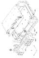


Classifications
-
- H—ELECTRICITY
- H01—ELECTRIC ELEMENTS
- H01R—ELECTRICALLY-CONDUCTIVE CONNECTIONS; STRUCTURAL ASSOCIATIONS OF A PLURALITY OF MUTUALLY-INSULATED ELECTRICAL CONNECTING ELEMENTS; COUPLING DEVICES; CURRENT COLLECTORS
- H01R12/00—Structural associations of a plurality of mutually-insulated electrical connecting elements, specially adapted for printed circuits, e.g. printed circuit boards [PCB], flat or ribbon cables, or like generally planar structures, e.g. terminal strips, terminal blocks; Coupling devices specially adapted for printed circuits, flat or ribbon cables, or like generally planar structures; Terminals specially adapted for contact with, or insertion into, printed circuits, flat or ribbon cables, or like generally planar structures
- H01R12/70—Coupling devices
- H01R12/71—Coupling devices for rigid printing circuits or like structures
- H01R12/72—Coupling devices for rigid printing circuits or like structures coupling with the edge of the rigid printed circuits or like structures
-
- H—ELECTRICITY
- H01—ELECTRIC ELEMENTS
- H01R—ELECTRICALLY-CONDUCTIVE CONNECTIONS; STRUCTURAL ASSOCIATIONS OF A PLURALITY OF MUTUALLY-INSULATED ELECTRICAL CONNECTING ELEMENTS; COUPLING DEVICES; CURRENT COLLECTORS
- H01R13/00—Details of coupling devices of the kinds covered by groups H01R12/70 or H01R24/00 - H01R33/00
- H01R13/46—Bases; Cases
-
- H—ELECTRICITY
- H05—ELECTRIC TECHNIQUES NOT OTHERWISE PROVIDED FOR
- H05K—PRINTED CIRCUITS; CASINGS OR CONSTRUCTIONAL DETAILS OF ELECTRIC APPARATUS; MANUFACTURE OF ASSEMBLAGES OF ELECTRICAL COMPONENTS
- H05K7/00—Constructional details common to different types of electric apparatus
- H05K7/02—Arrangements of circuit components or wiring on supporting structure
- H05K7/06—Arrangements of circuit components or wiring on supporting structure on insulating boards, e.g. wiring harnesses
Definitions
- the present invention relates to an electronic device.
- An automobile is equipped with a large number of ECUs (Electronic Control Units) for controlling an electric power steering device, an engine, a drive system and the like.
- the ECU which is an electronic device, is provided with a connector to which a connector (a mating connector) such as a power supply cable or a control signal cable is attached (see JP2010-63242A).
- JP 2010-63242 A describes that a DC conductor module having a power connector and a control module having a signal connector and a power module which is a circuit board are individually screwed to a metal casing.
- the DC conductor module is connected to the circuit board via a power lead frame (bus bar), and the control module is connected to the circuit board via a signal lead frame (bus bar).
- An object of the present invention is to improve the positioning accuracy of relative positions between a circuit board and a connector.
- an electronic device comprising: a base; a first circuit board fixed to the base; a bus bar unit fixed to the first circuit board; and the bus bar unit And a connector electrically connected to the first circuit board, the connector having a connection terminal and a terminal holding portion for holding the connection terminal, wherein one end of the bus bar unit is the first A bus bar connected to the circuit board and the other end connected to the connection terminal, and a bus bar holding member for holding the bus bar, the terminal holding portion being in contact with the reference surface of the first circuit board
- the reference surface is formed to be parallel to the contact surface of the bus bar in contact with the connection terminal.
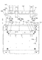
- FIG. 1 is an exploded perspective view showing an electronic device according to a first embodiment of the present invention.
- FIG. 2 is a perspective view showing an assembly in which the power substrate, the bus bar unit, and the connector are assembled to the heat dissipation base.
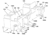
- FIG. 3A is a perspective view of the connector.
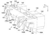
- FIG. 3B is a perspective view of the connector as viewed from a direction different from FIG. 3A.
- FIG. 4 is a perspective view of the heat dissipating base.
- FIG. 5 is a perspective view of the heat dissipating base on which the power substrate is attached.
- FIG. 6 is a perspective view of the heat dissipation base in which the bus bar unit is attached to the power substrate.
- FIG. 1 is an exploded perspective view showing an electronic device according to a first embodiment of the present invention.
- FIG. 2 is a perspective view showing an assembly in which the power substrate, the bus bar unit, and the connector are assembled to the heat dissipation base.
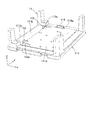
- FIG. 7 is a plan view of the heat dissipating base and the connector to which the power substrate is attached, showing a state before the connector is fixed to the heat dissipating base.
- FIG. 8 is a perspective view of the heat dissipation base with the connector positioned.
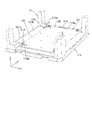
- FIG. 9 is a plan view of the heat dissipating base on which the power substrate is attached, and shows a state after the connector is fixed to the heat dissipating base.
- FIG. 10 is an enlarged cross-sectional view taken along the line XX in FIG. 9, and shows a connection structure of the fixing portion of the connector and the reinforcing portion of the support of the base.
- FIG. 11 is an enlarged sectional view taken along the line XI-XI in FIG. FIG.
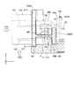
- FIG. 12 is a schematic view illustrating the regulation of the deformation in the first direction of the connector in the electronic device according to the first embodiment of the present invention.
- FIG. 13 is a schematic view illustrating the regulation of the deformation in the second direction of the connector in the electronic device according to the second embodiment of the present invention.
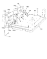
- FIG. 14 is an exploded perspective view of an electronic device according to a modification of the second embodiment of the present invention.
- FIG. 15 is a schematic view showing the shape of the connection terminal of the connector used in the electronic device according to the third embodiment of the present invention, and the positional relationship between the connection terminal and the first positioning projection.
- FIG. 16 is a schematic view showing the shape of the connection terminal of the connector used in the electronic device according to the modification of the third embodiment of the present invention, and the positional relationship between the connection terminal and the first positioning protrusion.
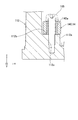
- FIG. 17 is a schematic cross-sectional view showing the restricting portion of the connector used in the electronic device according to the first modification.
- the electric power steering apparatus assists the driver's steering of the vehicle by controlling a motor for assisting the driver's steering force based on the steering torque of the steering wheel and the vehicle speed.
- the electronic control unit 100 controls the drive of the motor based on information output from a torque sensor, a vehicle speed sensor, or the like.
- the electronic control unit 100 includes a rectangular parallelepiped heat dissipating base 11, a power board (first circuit board) 13 as a circuit board fixed to the heat dissipating base 11, and a control board (second circuit board) 16, a bus bar unit 15 fixed to the power substrate 13, a connector 14 electrically connected to the power substrate 13 via the bus bar unit 15, and a rectangular box-shaped cover covering various components attached to the heat dissipation base 11 And 12.
- the heat dissipation base 11 is a heat sink that constitutes the bottom of the electronic control unit 100, and is a base formed of a metal material such as aluminum or an aluminum alloy.
- the heat dissipating base 11 is a flat plate portion 111 in a rectangular flat plate shape, a column 112 provided at four corners of the flat portion 111, and a pair of first positioning protrusions which project upward from the flat portion 111 and define the position of the power substrate 13. 113 and a second positioning protrusion 114.
- a rectangular mounting surface 111a on which the power substrate 13 is mounted is formed.
- the back surface of the power substrate 13 abuts on the mounting surface 111 a.
- the power substrate 13 is a circuit substrate responsible for driving a motor (not shown), and a bridge circuit including power semiconductor elements (not shown) such as MOSFETs and IGBTs is mounted.
- the power substrate 13 is a metal substrate formed of a metal material such as aluminum or an aluminum alloy.
- the control board 16 is mounted with a microcomputer for controlling a bridge circuit and the like mounted on the power board 13 and peripheral circuit elements, and is electrically connected to the power board 13.
- the control board 16 has a rectangular flat shape, and is disposed above the power board 13.
- the control substrate 16 is a glass epoxy based substrate.
- the power substrate 13 is disposed directly on the mounting surface 111 a of the flat plate portion 111 of the heat dissipation base 11 or via a flexible heat dissipation sheet or the like, and is fixed to the flat plate portion 111 by a screw.
- the control board 16 is supported by the four columns 112 and fixed to the tip of the column 112 by screws. By arranging the power substrate 13 having a larger amount of heat generation than the control substrate 16 on the mounting surface 111 a, the power substrate 13 can be cooled effectively. Further, by supporting the control board 16 by the support column 112, the control board 16 can be disposed at a predetermined distance from the power board 13 which is likely to generate heat. Therefore, the influence of the heat from the power board 13 on the control board 16 Can be reduced.
- the power substrate 13 and the control substrate 16 are arranged to overlap in the z-axis direction, which is the extending direction of the column 112.
- the dimensions of the electronic control unit 100 in the x direction and the y direction can be reduced as compared to the case where the power substrate 13 and the control substrate 16 are arranged side by side on the flat plate portion 111.
- the bus bar unit 15 is mounted on the power substrate 13.
- the bus bar unit 15 includes a bus bar 151 having one end electrically connected to the power substrate 13 and the other end electrically connected to a connection terminal 141 of the connector 14 described later, and a bus bar holding member 152 for holding the bus bar 151 Have.
- the bus bar holding member 152 is formed of a non-conductive resin material or the like, and is disposed along the surface of the power substrate 13, that is, along the xy plane.
- the plurality of bus bars 151 are integrally molded on the bus bar holding member 152, whereby the bus bar unit 15 is formed.
- the bus bar holding member 152 has a beam 153 extending along the y axis, and a pair of pillars 154 provided at both ends of the beam 153 and extending along the z axis, and has a portal shape.
- the lower ends of the pair of columns 154 are inserted into the pair of holes provided in the power substrate 13.
- the pair of columns 154 is inserted into the holes of the power substrate 13 to temporarily fix the bus bar unit 15 to the power substrate 13.
- a positioning pin 155 to be inserted into the positioning hole of the power substrate 13 is formed.
- the bus bar 151 is formed of a conductive metal material such as copper or nickel.
- the bus bar 151 is formed by bending a strip-like conductive plate.
- the bus bar 151 extends along the x-axis and is supported by the bus-bar holding member 152, and a terminal joint 151b extending upward along the z-axis from an end of the base 151a on the connector 14 side.
- a vertical portion 151c extending downward along the z-axis from an end opposite to the connector 14 in the base portion 151a, and a substrate bonding portion 151d extending along the x-axis from the lower end of the vertical portion 151c; Have.
- the terminal bonding portion 151 b has a contact surface that makes surface contact with the bus bar bonding portion 146 b of the connection terminal 141 of the connector 14 described later.
- the contact surface of the terminal bonding portion 151b in surface contact with the bus bar bonding portion 146b is formed to be parallel to the yz plane.
- the substrate bonding portion 151 d is bonded to a conductive land (not shown) disposed on the power substrate 13 by soldering.
- the cover 12 has a rectangular flat plate-like top plate 121 and four side plates 122 extending downward from four sides of the top plate 121.
- a rectangular opening 122b to which the connector 14 is attached is formed in one side plate 122A disposed parallel to the yz plane.
- the connector 14 is connected to a mating connector (not shown) of a cable that connects an external device (not shown) and the electronic control unit 100.
- the connector 14 is used to output the current from the plurality of bus bars 151 to a motor (not shown) provided outside the electronic control unit 100.
- the connector 14 includes a connection terminal 141 to which the other terminal of the other connector (not shown) is connected, a terminal holding portion 142 for holding the connection terminal 141, and the other connector (not shown). And a pair of fixing portions 140 fixed to the heat dissipation base 11. In addition, three or more fixing parts 140 may be provided.
- connection terminal 141 is formed of a conductive metal material such as copper or nickel.
- the connection terminal 141 is formed by bending a strip-like conductive plate.
- the connection terminal 141 is a base portion 145 (see FIGS. 9 and 11) embedded in the terminal holding portion 142, and a bus bar connection as a bus bar connection portion exposed from the terminal holding portion 142 and extending toward the bus bar unit 15 side.
- a plate 146 and an external conducting portion 147 (see FIGS. 9 and 11) exposed from the terminal holding portion 142 and extending toward the opposite side to the bus bar unit 15 are provided.
- the base portion 145 and the external conducting portion 147 are formed in a rectangular plate shape extending along the x-axis.
- the bus bar connecting plate 146 has a horizontal portion 146a extending along the x axis from the end of the base portion 145, and a bus bar joint 146b extending upward along the z axis from the end of the horizontal portion 146a. Form an L-shape in side view. That is, between the horizontal part 146a and the bus bar joint part 146b is a bent part 146c bent 90 degrees.
- the bus bar joint portion 146 b has a contact surface that makes surface contact with the terminal joint portion 151 b of the bus bar 151 described above.
- the contact surface of the bus bar joint 146 b in surface contact with the terminal joint 151 b is formed to be parallel to the yz plane.
- the bus bar joint portion 146 b is joined to the terminal joint portion 151 b by welding.
- the path length of the bus bar connection plate 146 can be made longer as compared with the case where the bent portion is not provided. As a result, it is possible to suppress the influence exerted by the external force generated in the connector 14 on the connection portion between the connection terminal 141 and the bus bar 151, and to reduce the stress generated in the connection portion.
- the terminal holding portion 142 is formed of a non-conductive resin material or the like, and is formed in a substantially rectangular parallelepiped shape in which the y-axis direction is a longitudinal direction.
- the mounting portion 143 has a recess into which the mating connector is fitted, and an external conducting portion 147 (see FIGS. 9 and 11) to which the mating terminal of the mating connector is electrically connected is disposed inside.
- the terminal holding portion 142 includes a pair of belt-like flat plates 190A and 190B facing each other, a pair of connecting plates 148 connecting both ends of the pair of belt-like flat plates 190A and 190B in the y-axis direction, and a pair of connecting plates 148 The plurality of reinforcing plates 149 connecting the strip-like flat plates 190A and 190B to each other and the plurality of embedded portions 144 in which the base portion 145 of the connection terminal 141 is embedded.
- one belt-like flat plate 190 ⁇ / b> A of the pair of belt-like flat plates 190 ⁇ / b> A and 190 ⁇ / b> B is a decorative board covering the opening 122 b of the cover 12.
- the connector 14 is fixed to the heat dissipation base 11 by a screw 195. The details of the positioning structure and fixing structure of the connector 14 with respect to the heat dissipation base 11 will be described later.
- the mounting surface 111 a is formed at a position slightly higher than the peripheral region 111 b around the mounting surface 111 a.
- the mounting surface 111a and the peripheral region 111b may be formed flush with each other.
- the flat plate portion 111 is provided with a pair of first positioning protrusions 113 and a single second positioning protrusion 114 protruding upward from the peripheral region 111b.
- the pair of first positioning protrusions 113 is in the shape of a rectangular flat plate, and is disposed along one side of the mounting surface 111 a extending along the y axis.
- the single second positioning projection 114 is in the form of a rectangular flat plate, and is disposed along one side extending along the x-axis of the mounting surface 111a.
- the power substrate 13 is mounted on the mounting surface 111 a and fixed to the heat dissipation base 11 by screws.
- One side surface of the power substrate 13 extending along the y-axis is formed as a first reference surface 131.
- One side surface of the power substrate 13 extending along the x-axis is formed as a second reference surface 132.
- the first positioning protrusion 113 has an x-axis inner contact surface 113 a that contacts the first reference surface 131 of the power substrate 13.
- the x-axis inner contact surface 113 a and the first reference surface 131 are flat surfaces parallel to the yz plane.
- the pair of first positioning protrusions 113 abuts on the first reference surface 131 of the power substrate 13 to define the position of the power substrate 13 with respect to the heat dissipation base 11 in the x-axis direction.
- the x-axis direction is defined based on the power substrate 13, the x-axis direction is a direction orthogonal to the first reference surface 131 of the power substrate 13.
- the second positioning projection 114 has a y-axis inner abutment surface 114 a that abuts on the second reference surface 132 of the power substrate 13.
- the y-axis inner contact surface 114 a and the second reference surface 132 are flat surfaces parallel to the xz plane.
- the single second positioning protrusion 114 abuts on the second reference surface 132 of the power substrate 13 to define the position of the power substrate 13 with respect to the heat dissipation base 11 in the y-axis direction.
- the y-axis direction is a direction orthogonal to the second reference surface 132 of the power substrate 13, that is, a direction parallel to the first reference surface 131 of the power substrate 13.
- An example of the procedure for attaching the power substrate 13 to the heat dissipation base 11 is as follows.
- the first reference surface 131 of the power substrate 13 is brought into contact with each of the x-axis inner contact surfaces 113 a of the pair of first positioning protrusions 113.
- the power substrate 13 is slid in the y-axis direction while maintaining the first reference surface 131 in contact with the first positioning projection 113.
- the power substrate 13 is slid until the second reference surface 132 abuts on the y-axis inner contact surface 114 a of the second positioning projection 114.
- the attachment of the power substrate 13 to the heat dissipation base 11 is completed.
- the power substrate 13 As described above, by arranging the power substrate 13 such that the first reference surface 131 abuts on the pair of first positioning protrusions 113, positioning of the power substrate 13 with respect to the heat dissipation base 11 in the x-axis direction can be performed easily and accurately. be able to. Furthermore, by arranging the power substrate 13 so that the second reference surface 132 abuts on the second positioning projection 114, the positioning of the power substrate 13 with respect to the heat dissipation base 11 in the y-axis direction can be performed easily and accurately.
- the bus bar unit 15 is fixed to the power substrate 13.
- An example of the procedure for attaching the bus bar unit 15 to the power substrate 13 is as follows.
- the positioning pins 155 of the bus bar unit 15 are fitted into the positioning holes of the power substrate 13, and the pair of pillars 154 are inserted into the pair of holes provided in the power substrate 13.
- the substrate bonding portion 151 d of the bus bar 151 is soldered to the land of the power substrate 13, and the substrate bonding portion 151 d is bonded to the power substrate 13.
- the terminal holding portion 142 of the connector 14 is provided with a pair of L-shaped convex portions 180A and 180B that exhibit an L shape when the connecting plate 148 is viewed from the z-axis direction.
- the L-shaped convex portion 180A protruding from one of the pair of connecting plates 148 is a first flat surface 181 which is a flat surface parallel to the yz plane and a second flat surface 182 which is a flat surface parallel to the xz plane.
- the L-shaped convex portion 180B protruding from the other of the pair of connecting plates 148 is a first flat surface 181 which is a flat surface parallel to the yz plane and a second flat surface 182 which is a flat surface parallel to the xz plane. And.
- the first flat surface 181 of the L-shaped convex portions 180A and 180B abuts on the first reference surface 131 of the power substrate 13.
- the power substrate 13 defines the position of the connector 14 with respect to the heat dissipation base 11 in the x-axis direction by contacting the first flat surface 181 as the first contact surface.
- the x-axis direction is defined based on the connector 14, the x-axis direction is a direction orthogonal to the first plane 181 of the connector 14.
- One of the pair of first positioning protrusions 113 of the heat dissipating base 11 described above (the first positioning protrusion 113 on the right side in the figure) abuts on the second flat surface 182 of the L-shaped convex portion 180A of the connector 14 It has a contact surface 113b.
- the y-axis outer contact surface 113 b is a flat surface parallel to the xz plane.
- the first positioning projection 113 abuts on a second flat surface 182 as a second contact surface of the L-shaped convex portion 180A of the connector 14 to thereby define the position of the connector 14 with respect to the heat dissipation base 11 in the y-axis direction. .
- the y-axis direction is a direction orthogonal to the second plane 182 of the connector 14, that is, a direction parallel to the first plane 181 of the connector 14.
- the L-shaped convex portion 180B of the connector 14 has the same shape as the L-shaped convex portion 180A and has the second flat surface 182, but the pair of first positioning protrusions 113 It does not abut on the other (the first positioning projection 113 on the left side in the figure).
- the first positioning projection 113 on the right side of the drawing has a function of defining the position of the connector 14 in the y-axis direction with respect to the heat dissipating base 11 in addition to the function of defining the position of the power substrate 13 with respect to the heat dissipating base 11 in the x-axis direction. Therefore, compared to the case where the member for defining the position of the power substrate 13 in the x-axis direction with respect to the heat dissipating base 11 and the member for defining the position of the connector 14 in the y-axis direction with respect to the heat dissipating base 11 are provided separately The manufacturing cost of the control unit 100 can be reduced.
- the connector 14 is placed on the reinforcing portion 112 a of the support 112 of the heat dissipation base 11 and fixed to the reinforcing portion 112 a by the screw 195.
- the reinforcing portion 112 a is a protruding portion that protrudes from the column main body in the x-axis direction at the proximal end portion of the support column 112.
- the upper surface of the reinforcing portion 112 a is a flat surface parallel to the xy plane, and is a positioning surface 112 b that defines the position of the connector 14 in the z-axis direction with respect to the heat dissipation base 11 by abutting on the fixing portion 140 of the connector 14. . That is, the connector 14 is attached in a direction (z-axis direction) orthogonal to the positioning surface 112 b of the heat dissipation base 11.
- the base end side of the reinforcing portion 112 a is continuous with the flat plate portion 111, and has a function of suppressing deformation of the support column 112 and the heat dissipating base 11. Furthermore, the reinforcing portion 112 a also has a function as a mounting table that defines the position of the connector 14 in the z-axis direction with respect to the heat dissipation base 11 by mounting the connector 14. Therefore, the manufacturing cost of the electronic control unit 100 can be reduced as compared with the case where the reinforcing portion 112 a and the mounting table are provided separately.
- the fixing portion 140 of the connector 14 is fixed to the reinforcing portion 112 a of the support 112 by the screw 195. As shown in FIGS. 7 and 9, the fixing portion 140 is provided so as to protrude outward in the y-axis direction from the pair of connecting plates 148 of the terminal holding portion 142.
- the fixing portion 140 is provided with a through hole penetrating in the z-axis direction, and a metal collar 140a is inserted into the through hole.
- the collar 140a is formed in a cylindrical shape and is fixed so as not to cause displacement in the through hole.
- the collar 140a is fixed to the through hole, for example, by insert molding. In this case, it is preferable to provide a recess or a protrusion on the outer peripheral surface of the collar 140a so that the collar 140a is not displaced in the through hole.
- both ends of the collar 140 a protrude from the fixing portion 140.
- the lower end surface of the collar 140 a abuts on the upper surface (the positioning surface 112 b) of the reinforcing portion 112 a of the support column 112.
- the shaft portion of the screw 195 is inserted into the inside of the collar 140a.
- a male screw portion is formed to be screwed to a female screw portion formed on the inner peripheral surface of the screw hole 112c of the reinforcing portion 112a.
- the screw holes 112 c may not penetrate the heat dissipation base 11 as shown in the drawing, or may penetrate the heat dissipation base 11.
- An example of the procedure for attaching the connector 14 to the heat dissipation base 11 is as follows. As shown in FIG. 8, the pair of fixing portions 140 of the connector 14 is mounted on the reinforcing portion 112 a of the column 112 which is a mounting table.
- the first flat surface 181 of the L-shaped convex portions 180A and 180B is brought into contact with the first reference surface 131 of the power substrate 13 fixed to the heat dissipation base 11.
- the connector 14 is slid in the y-axis direction while maintaining the L-shaped convex portions 180A and 180B in contact with the first reference surface 131.
- the connector 14 is slid until the second flat surface 182 of the L-shaped convex portion 180A abuts on the y-axis outer side contact surface 113b of the first positioning projection 113 disposed on the right side of the drawing.
- the screw 195 is passed through the inside of the collar 140a, and the male screw formed at the tip of the screw 195 is screwed into the female screw of the screw hole 112c of the reinforcing portion 112a.
- the connector 14 is fixed to the reinforcing portion 112 a by the screw 195, the attachment of the connector 14 to the heat dissipation base 11 is completed.
- terminal junction 151b of bus bar 151 and busbar junction 146b of connection terminal 141 are brought into surface contact with each other to make terminal junction 151b and busbar junction.
- Join with 146b by welding.
- the welding method can employ various methods such as TIG welding, laser welding, electron beam welding, and the like.
- the bus bar 151 and the connection terminal 141 may be joined by another joining method such as adhesion with conductive adhesive or pressure bonding.
- the metal collar 140 a By mounting the metal collar 140 a on the reinforcing portion 112 a as a metal mounting table, positioning of the connector 14 with respect to the heat dissipation base 11 in the z-axis direction can be performed easily and accurately.
- the positioning accuracy of the relative position in the z-axis direction between the bus bar joint 146 b of the connection terminal 141 and the terminal joint 151 b of the bus bar 151 can be improved.
- the front end surface (upper end surface) of the bus bar joint portion 146 b and the front end surface (upper end surface) of the terminal joint portion 151 b can be set substantially flush. Thereby, the welding workability between the end of the bus bar joint 146b and the end of the terminal joint 151b can be improved.
- the power substrate 13 is positioned in the y-axis direction with respect to the heat dissipation base 11 by the second positioning protrusion 114. Therefore, by positioning the connector 14 in the y-axis direction with respect to the heat dissipation base 11, the relative position between the power substrate 13 and the connector 14 in the y-axis direction can be determined. Thus, the positioning accuracy of the relative position in the y-axis direction between the bus bar joint 146 b of the connection terminal 141 and the terminal joint 151 b of the bus bar 151 can be improved.
- the screw 195 for fixing the connector 14 to the heat dissipation base 11, the screw for fixing the power substrate 13 to the heat dissipation base 11, and the screw for fixing the control substrate 16 to the heat dissipation base 11 are all z. Arranged parallel to the axis. For this reason, the worker only needs to attach a screw from the upper side of the heat dissipation base 11, so that the workability is good.
- the electronic control unit 100 is manufactured by a work machine instead of the worker, the electronic control unit 100 can be completed only by access from above in the manufacturing line. Thereby, the manufacturing efficiency can be improved, and the manufacturing cost of the electronic control unit 100 can be reduced.
- the lower end portion of the belt-like flat plate (decorative plate) 190A is a projecting portion 191 that protrudes below the bottom surfaces of the connection plate 148 and the reinforcing plate 149.
- the protrusion 191 extends from one connecting plate 148 to the other connecting plate 148.
- a step is formed at the corner on the upper end side in the thickness direction (z-axis direction) of the flat plate portion 111 of the heat dissipation base 11.
- the upper surface of the step (hereinafter referred to as the step surface 111c) is located closer to the bottom surface of the flat portion 111 of the heat dissipation base 11 than the mounting surface 111a and the peripheral region 111b of the power substrate 13.
- the protrusion 191 of the connector 14 and the step surface 111 c of the heat dissipating base 11 are disposed to face each other in the z-axis direction.
- the position of the connector 14 in the z-axis direction with respect to the heat dissipation base 11 is defined by the reinforcing portion 112 a of the support 112 and the collar 140 a of the fixing portion 140.
- a gap 199 in the z-axis direction is formed between the peripheral edge region 111 b of the flat plate portion 111 and the bottom surface of the terminal holding portion 142.
- the projecting portion 191 protrudes from the bottom surface of the terminal holding portion 142 toward the step surface 111 c and covers the gap 199 between the peripheral region 111 b of the flat plate portion 111 and the bottom surface of the terminal holding portion 142.
- the gap 199 between the peripheral area 111b of the flat plate portion 111 and the bottom surface of the terminal holding portion 142 is configured so as not to be visible from the outside by the protruding portion 191, the appearance can be improved.
- the projecting portion 191 it is possible to suppress foreign matter such as dust and water droplets from invading the inside of the electronic control unit 100.
- the protruding portion 191 has a function as a restricting portion which restricts the deformation of the connector 14 and reduces the stress generated in the welded portion 170, in addition to the function of improving the appearance.
- the position of the connector 14 in the z-axis direction with respect to the heat dissipation base 11 is defined by the reinforcing portion 112 a of the support 112 and the collar 140 a of the fixing portion 140. Therefore, a predetermined gap 198 is formed between the protrusion 191 and the step surface 111c.
- the dimension D1 of the gap 198 is set to a value as small as possible within the range in which the tolerance can be absorbed, in order to suppress the amount of bending (the amount of deformation) of the connector 14 which is deformed due to the external force acting on the connector 14.
- an external force F 11 that pulls the connector 14 toward the outside of the electronic control unit 100 or an external force F 12 that pushes the connector 14 downwards is
- a rotational moment M1 acts on the connector 14 with the boundary portion between the fixing portion 140 and the reinforcing portion 112a in the shaft portion of the screw 195 as a fixing fulcrum P.
- the connector 14 bends (deforms) counterclockwise in the drawing.
- the protrusion 191 is not in contact with the step surface 111c when no external force is applied to the connector 14, and contacts the step surface 111c when external forces F11 and F12 are applied to the connector 14 Regulate the deflection of 14
- the contact area between the connector 14 and the heat dissipation base 11 temporarily increases. Thereby, when external force F11 or external force F12 acts on connector 14, it is possible to reduce the stress generated in welded portion 170 between connection terminal 141 of connector 14 and bus bar 151.
- the positioning surface 112b of the heat dissipating base 11 on which the fixing portion 140 is mounted is set at a position higher than the mounting surface 111a by a predetermined height.
- the engagement margin of the screw 195 can be made longer, and the connection strength and stability of the connector 14 to the heat dissipation base 11 can be improved.
- the projection 191 is between the peripheral area 111 b of the mounting surface 111 a on which the power substrate 13 is mounted and the terminal holder 142 of the connector 14.
- Has a function of covering the gap 199 of Therefore, it is not necessary to provide a dedicated part having only the function of covering the gap 199 between the peripheral area 111b of the mounting surface 111a and the terminal holding part 142 separately from the restricting part. Therefore, the manufacturing cost of the electronic control unit 100 can be reduced.
- the terminal holding portion 142 has a first flat surface 181 in direct contact with the first reference surface 131 of the power substrate 13.
- the first reference surface 131 is parallel to the contact surface of the bus bar 151 in contact with the connection terminal 141. It is formed to be Therefore, by arranging the connector 14 so that the first flat surface 181 of the connector 14 abuts on the first reference surface 131 of the power substrate 13, positioning of the relative position between the power substrate 13 and the connector 14 in the x-axis direction can be achieved. It can be done easily and accurately. That is, the relative position between the bus bar 151 connected to the power substrate 13 and the connection terminal 141 of the connector 14 can be easily and accurately positioned.
- connection terminal 141 and the bus bar 151 can be improved, the occurrence of welding defects can be reduced when welding the connection terminal 141 and the bus bar 151. Further, since positioning can be easily performed with high accuracy, the number of manufacturing steps of the electronic control unit 100 can be reduced, and the manufacturing cost can be reduced.
- a projecting portion as a restricting portion that restricts the bending (deformation) of the connector 14 by contacting the heat dissipation base 11 when an external force acts on the connector 14 by inserting and removing the mating connector in the connector 14 191 is provided. Therefore, when an external force is applied to the connector 14, the bending (deformation) of the connector 14 is restricted by the protrusion 191. Thereby, when an external force acts on the connector 14, it is possible to reduce the stress generated in the welded portion 170 which is a connection portion between the connection terminal 141 of the connector 14 and the bus bar 151. When no external force is applied to the connector 14 for inserting and removing the mating connector, the protrusion 191 does not contact the heat dissipation base 11. Therefore, when positioning the connector 14 with respect to the bus bar unit 15, the protrusion 191 does not disturb the positioning operation. That is, the protrusion 191 as the restricting portion does not interfere with the alignment between the connector 14 and the bus bar unit 15.
- the terminal holding portion 242 is formed longer in the x-axis direction than the terminal holding portion 142 of the first embodiment, and the lower end portion of the strip-like flat plate 190B is configured as the restricting portion 291.
- the protrusion 191 is provided at a predetermined distance away in the x-axis direction (left in the figure) than the fixed fulcrum P, and the restricting part 291 is predetermined in the other (right in the figure) in the x-axis direction than the fixed fulcrum P It is provided at a distance.
- a predetermined gap 298 is formed between the restricting portion 291 and the peripheral region 111b.
- the dimension D2 of the gap 298 is set as small as possible within the range in which the tolerance can be absorbed, in order to suppress the amount of bending (the amount of deformation) of the connector 214 that is deformed due to the external force acting on the connector 214.
- an external force F21 which pushes the connector 214 toward the inside of the electronic control unit 100 when inserting the mating connector into the connector 214 or an external force F22 which pushes the connector 214 upward acts, as shown in FIG.
- a rotational moment M2 acts on the connector 214.
- the connector 214 bends (deforms) clockwise in the figure.
- the restriction portion 291 of the strip-like flat plate 190B is disposed to face the peripheral region 111b.
- the restricting portion 291 is not in contact with the peripheral area 111b when no external force is applied to the connector 214, and contacts the peripheral area 111b when external forces F21 and F22 are applied to the connector 214, thereby bending the connector 214. regulate.
- the contact area between the connector 214 and the heat dissipation base 11 temporarily increases. Thereby, when external force F21 or external force F22 acts on connector 214, it is possible to reduce the stress generated in welded portion 170 which is a connection portion between connection terminal 141 of connector 214 and bus bar 151.
- the second embodiment in addition to the effects of the first embodiment, even when the external force F21 or the external force F22 acts on the connector 214, it is possible to suppress the bending of the connector 214. That is, according to the second embodiment, when attaching or detaching the mating connector to / from the mounting portion 143, it is possible to restrict the bending of the connector 214 caused by the external force from various directions generated in the connector 214. Thereby, the stress generated in the welding portion 170 which is a connection portion between the connection terminal 141 of the connector 214 and the bus bar 151 can be more effectively reduced.
- the upper end portion of the belt-like flat plate 190A may be configured as the restricting portion 391.
- the pair of columns 322 aligned in the y-axis direction is provided with protrusions 322 b protruding inward in the y-axis direction.
- a restricting portion 391 of a strip-like flat plate 190A which is a decorative plate of the connector 314 is disposed to face the projecting portion 322b. The restricting portion 391 is not in contact with the projecting portion 322b when no external force is applied to the connector 314, and contacts the projecting portion 322b when external forces F21 and F22 are applied to the connector 314, thereby bending the connector 314. regulate.
- the bus bar connecting plate 446 of the connection terminal 441 of the connector 414 has three bent portions 441a, 441b and 441c.
- the bus bar connection plate 446 has a step-like shape in a side view.
- the bus bar connecting plate 446 includes a first extending portion 446a extending from the terminal holding portion 142, a second extending portion 446b extending from a tip end of the first extending portion 446a, and a second extending portion 446b.
- a third extending portion 446c extending from the tip end and a bus bar joint portion 146b extending from the tip end of the third extending portion 446c.
- the first extending portion 446 a is provided parallel to the xy plane, and extends from the terminal holding portion 142 toward the first positioning protrusion 113.
- the second extending portion 446 b is formed by bending the tip end portion of the first extending portion 446 a 90 degrees as the bending portion 441 a.
- the second extending portion 446 b is provided in parallel to the yz plane, and extends upward from the tip end of the first extending portion 446 a, that is, in a direction away from the flat plate portion 111.
- the third extending portion 446c is formed by bending the tip end portion of the second extending portion 446b by 90 degrees as the bending portion 441b.
- the third extending portion 446 c is provided in parallel to the xy plane, and extends from the tip of the second extending portion 446 b toward the terminal bonding portion 151 b of the bus bar 151.
- the bus bar joint portion 146 b is formed by bending the tip end portion of the third extending portion 446 c as a bending portion 441 c by 90 degrees.
- the bus bar joint portion 146 b is provided parallel to the yz plane, and extends upward from the tip end of the third extending portion 446 c, that is, in the direction away from the flat plate portion 111.
- the tip of the bus bar joint 146 b is joined to the terminal joint 151 b of the bus bar 151.
- the third extending portion 446 c is disposed to pass immediately above the first positioning protrusion 113. That is, by setting the bending portion 441a, which is the boundary between the first extending portion 446a and the second extending portion 446b, between the first positioning projection 113 and the mounting portion 143, the connection terminal 441 and the first positioning projection can be obtained. Interference with 113 is avoided.
- the bus bar connection plate 446 is provided with a greater number of bent portions than in the first embodiment.
- the path length of the bus bar connecting plate 446 from the terminal holding portion 142 to the bus bar 151 can be made longer than the path length of the bus bar connecting plate 146 of the first embodiment. It can be absorbed. Therefore, when an external force is generated in connector 414, it is possible to suppress the influence of the bending of connector 414 on weld 170 which is the connection portion between bus bar connection plate 446 and bus bar 151. As a result, it is possible to further reduce the stress generated in weld portion 170 which is a connection portion between bus bar connection plate 446 and bus bar 151.
- the path length of the bus bar connecting plate 446 can be increased while reducing the dimension in the x-axis direction of the electronic control unit 100. . Furthermore, in the third embodiment, since the bus bar connection plate 446 and the first positioning projection 113 can be arranged to overlap each other when viewed from the z-axis direction, the electronic control unit 100 in the y-axis direction The dimensions can be reduced. That is, according to the third embodiment, the degree of freedom in the arrangement of the connection terminals 441 can be improved.
- the bus bar connecting plate 446 having a step-like side view is described, but the present invention is not limited to this.
- the bus bar connection plate 546 of the connection terminal 541 of the connector 514 may be provided with a U-shaped folded portion in a side view.
- the bus bar connecting plate 546 is bent by 90 degrees from the end of the first extending portion 546a extending from the terminal holding portion 142 toward the first positioning projection 113 and the end of the first extending portion 546a, and extends upward.
- the third extending portion 546c and the bus bar joint portion 146b bent 90 degrees from the end of the third extending portion 546c and extending upward are provided.
- the third extending portion 546 c of the connection terminal 541 is disposed to pass immediately above the first positioning protrusion 113. According to such a configuration, the same effects as those of the third embodiment can be obtained.
- FIG. 17 is a schematic cross-sectional view showing the restricting portion of the connector 14 used in the electronic device according to the first modification.
- a protrusion 111 d protruding upward from the peripheral region 111 b is provided in the peripheral region 111 b of the mounting surface 111 a of the heat dissipation base 11.
- the bottom surface of the terminal holding portion 142 of the connector 14 is provided with a recess 691 into which the protrusion 111 d is inserted.
- the protrusion 111 d is provided to extend in the y-axis direction between the pair of columns 112 disposed on the connector 14 side.
- the recess 691 extends in the y-axis direction from one connecting plate 148 to the other connecting plate 148.
- the protrusion 111 d covers the gap 199 between the peripheral region 111 b of the flat plate portion 111 and the bottom surface of the terminal holding portion 142.
- the recess 691 functions as a restricting portion that restricts the deformation of the connector 14 in the first direction in the counterclockwise direction in the drawing. That is, when the external forces F11 and F12 act on the connector 14, the bottom surface of the recess 691 contacts the tip of the protrusion 111d, whereby the bending of the connector 14 is restricted. According to such a first modification, the same operation and effect as those of the first embodiment can be obtained.
- Modification 3 Although the said embodiment supports the example which the base which supports a circuit board is formed as the thermal radiation base 11, this invention is not limited to this. The present invention can also be applied to an electronic device in which a circuit board is supported on a support base that does not have a heat dissipation function.
- a flat surface is provided as a contact surface for contacting the first reference surface 131 of the power substrate 13 with each of the pair of L-shaped convex portions 180A and 180B provided in the terminal holding portion 142 of the connector 14
- the present invention is not limited thereto.
- a curved surface (arc surface) exhibiting a semicircular shape in plan view may be provided.
- the curved surfaces (arc surfaces) provided at two locations of the terminal holding portion 142 abut on the first reference surface 131 of the power substrate 13 to define the relative position between the power substrate 13 and the connector 14. Ru.
- the power substrate 13 By bringing at least the first reference surface 131 of the power substrate 13 into contact with the first flat surface 181 of the connectors 14, 214, 314, 414, 514, the power substrate 13 and the connectors 14, 214, 314, 414, 514 Positioning of the relative position of can be performed with high accuracy.
- the method of positioning the power substrate 13 with respect to the heat dissipation base 11 is not limited to the above embodiment.
- the power substrate 13 may be positioned with respect to the heat dissipating base 11 based on the mark attached to the heat dissipating base 11, and the power substrate 13 may be fixed to the heat dissipating base 11 with a screw.
- Modification 12 Although the said embodiment demonstrated the electronic control unit 100 provided with two circuit boards, this invention is not limited to this.
- the present invention may be applied to an electronic device provided with a single circuit board having the functions of the power board 13 and the control board 16.
- the electronic control unit 100 as an electronic device includes a heat dissipation base 11 as a base, a power board 13 as a first circuit board fixed to the heat dissipation base 11, a bus bar unit 15 fixed to the power board 13, and a bus bar unit Connectors 14, 214, 314, 414, 514 electrically connected to the power substrate 13 via the connector 15, and the connectors 14, 214, 314, 414, 514 have connection terminals 141, 441, 541, respectively.
- the bus bar unit 15 has a terminal holding portion 142, 242 for holding the connection terminals 141, 441, 541.
- the bus bar unit 15 has one end connected to the power substrate 13 and the other end connected to the connection terminals 141, 441, 541.
- first flat surface 181 as a first contact surface to be in contact with the first reference surface 131 as a reference surface of the power substrate 13, and the first reference surface 131 contacts the connection terminals 141, 441, 541 It is formed to be parallel to the contact surface of bus bar 151.
- the heat dissipating base 11 has a flat plate portion 111 and a first positioning projection 113 projecting from the flat portion 111.
- the first positioning projection 113 is orthogonal to the first reference surface 131.
- the position of the power substrate 13 with respect to the heat dissipation base 11 in the x-axis direction, which is the first direction to be performed, is defined.
- the first positioning protrusion 113 of the heat dissipation base 11 can easily position the power substrate 13 with respect to the heat dissipation base 11 in the x-axis direction.
- the heat dissipation base 11 has a second positioning protrusion 114 protruding from the flat plate portion 111, and the second positioning protrusion 114 is in the y-axis direction which is a second direction parallel to the first reference surface 131.
- the position of the power substrate 13 with respect to the heat dissipation base 11 is defined.
- the second positioning protrusion 114 of the heat dissipation base 11 can easily position the power substrate 13 with respect to the heat dissipation base 11 in the y-axis direction.
- the electronic control unit 100 has a second flat surface 182 as a second contact surface in which the connectors 14, 214, 314, 414, 514 contact the first positioning protrusion 113, and the second positioning flat surface 113
- the contact with the contact 182 defines the position in the y-axis direction.
- the connectors 14, 214, 314, 414, 514 with respect to the heat dissipating base 11 It has the function of defining the position. Therefore, a member defining the position of the power substrate 13 in the x-axis direction with respect to the heat dissipating base 11 and a member defining the position of the connectors 14, 214, 314, 414, 514 in the y-axis direction with respect to the heat dissipating base 11 are separately provided.
- the manufacturing cost of the electronic control unit 100 can be reduced as compared to the case where the electronic control unit 100 is provided.
- the heat dissipating base 11 has a mounting table (reinforcement portion 112a) made of metal, and a fixing portion in which the connectors 14, 214, 314, 414, 514 are fixed to the mounting table (reinforcement portion 112a)
- the connector 14, 214, 314, 414, 514 has the collar 140 a mounted on the mounting table (the reinforcing portion 112 a), whereby the position in the z-axis direction is defined.
- the connectors 14, 214, 314, 414, 514 can be accurately positioned in the z-axis direction. it can.
- the electronic control unit 100 has a support 112 for supporting the second circuit board (control board 16) different from the first circuit board (power board 13) in the heat dissipation base 11.
- the second circuit board (control board 16) is supported by the pillars 112, and the first circuit board (power board 13) and the second circuit board (control board 16) overlap in the extending direction of the pillars 112.
- the size of the electronic control unit 100 in the direction orthogonal to the extending direction of the support 112 can be reduced.
- a reinforcing portion 112a which is a projecting portion protruding laterally from the column main body of the column 112, is used as a mounting table.
- the reinforcing portion 112a that protrudes laterally from the column main body has a function of suppressing the bending of the support and the heat dissipation base 11, and as a mounting table to which the connectors 14, 214, 314, 414, 514 are fixed. It has a function. Therefore, the manufacturing cost of the electronic control unit 100 can be reduced as compared with the case where the reinforcing portion 112 a and the mounting table are provided separately.
- connection terminals 141, 441, 541 have bus bar connection plates 146, 446, 546 as bus bar connection portions connected to the bus bars 151, and the bus bar connection plates 146, 446, 546 are bent portions 146c, 441a, 441b, 441c.
- the path lengths of the bus bar connection plates 146, 446, 546 can be made longer. This suppresses the influence exerted by the external force generated on connectors 14, 214, 314, 414, 514 on the connection portion (welding portion 170) between connection terminals 141, 441, 541 and bus bar 151, and this connection portion (welding portion 170). Stress) can be reduced.
- connection terminals 441 and 541 are bent from the first extending portions 446a and 546a extending from the terminal holding portion 142 toward the first positioning projection 113 and the first extending portions 446a and 546a.
- a third extending portion 446c extending from the second extending portions 446b and 546b extending in a direction away from the flat plate portion 111 and from the second extending portions 446b and 546b and passing immediately above the first positioning projection 113.
- 546 c, and a bus bar joint 146 b extending from the third extension 446 c, 546 c and joined to the bus bar 151.
- connection terminals 441 and 541 when the connection terminals 441 and 541 are disposed immediately above the first positioning projection 113, the connection terminals 441 and 541 can avoid interference with the first positioning projection 113. Since the connection terminals 441 and 541 can be disposed immediately above the first positioning projection 113, the degree of freedom in the arrangement of the connection terminals 441 and 541 can be improved.
- the restricting portions (191, 291, 391 When the connectors 14, 214, 314, 414, 514 and the bus bar unit 15 are electrically connected by preventing the contact 691) from contacting the heat dissipation base 11, the connectors 14, 214, 314, 414, 514 The restriction portions (191, 291, 391, 691) do not interfere with the alignment between the connectors 14, 214, 314, 414, 514 and the bus bar unit 15.
- the restriction portions (191, 291, 391, 691) of the connectors 14, 214, 314, 414, 514 release the heat radiation base 11.
- Contact with the connector 14 can reduce stress applied to the connection portion (welding portion 170) of the connector 14, 214, 314, 414, 514 and the bus bar unit 15, and can suppress damage to the connection portion (welding portion 170). .
Landscapes
- Engineering & Computer Science (AREA)
- Microelectronics & Electronic Packaging (AREA)
- Cooling Or The Like Of Electrical Apparatus (AREA)
- Coupling Device And Connection With Printed Circuit (AREA)
- Connector Housings Or Holding Contact Members (AREA)
Abstract
電子機器(100)は、ベース(11)と、ベース(11)に固定される回路基板(13)と、回路基板(13)に固定されるバスバーユニット(15)と、バスバーユニット(15)を介して回路基板(13)に接続されるコネクタ(14)と、を備え、コネクタ(14)は、接続端子(141)と、端子保持部(142)と、を有し、バスバーユニット(15)は、回路基板(13)及び接続端子(141)に接続されるバスバー(151)と、バスバー保持部材(152)と、を有し、端子保持部(142)は、回路基板(13)の基準面(131)に当接する第1当接面(181)を有し、基準面(131)は、接続端子(141)に接触するバスバー(151)の接触面と平行となるように形成される。
Description
本発明は、電子機器に関する。
自動車には、電動パワーステアリング装置やエンジン、駆動系等を制御する多数のECU(Electronic Control Unit)が搭載されている。電子機器であるECUには、電源用のケーブルや制御信号用のケーブル等のコネクタ(相手コネクタ)が装着されるコネクタが設けられている(JP2010-63242A参照)。
JP2010-63242Aには、電源コネクタを備えるDC導体モジュール及び信号コネクタを備える制御モジュール、回路基板であるパワーモジュールが、それぞれ個別に金属製筐体にネジ止めされることが記載されている。DC導体モジュールはパワーリードフレーム(バスバー)を介して回路基板に接続され、制御モジュールは信号用リードフレーム(バスバー)を介して回路基板に接続される。
しかしながら、コネクタを有するモジュールと回路基板とをそれぞれ個別に筐体にネジ止めする場合、モジュールと回路基板との相対位置を精度よく位置決めすることが難しい。精度よく位置決めできない場合、たとえば、回路基板に接続されるリードフレーム(バスバー)と、モジュールのコネクタの接続端子と、の間に隙間が生じた状態で溶接がなされることに起因して、溶接不良が発生するおそれがある。
本発明は、回路基板とコネクタとの相対位置の位置決め精度を向上することを目的とする。
本発明のある態様によれば、電子機器であって、ベースと、前記ベースに固定される第1回路基板と、前記第1回路基板に固定されるバスバーユニットと、前記バスバーユニットを介して前記第1回路基板に電気的に接続されるコネクタと、を備え、前記コネクタは、接続端子と、前記接続端子を保持する端子保持部と、を有し、前記バスバーユニットは、一端が前記第1回路基板に接続され他端が前記接続端子に接続されるバスバーと、前記バスバーを保持するバスバー保持部材と、を有し、前記端子保持部は、前記第1回路基板の基準面に当接する第1当接面を有し、前記基準面は、前記接続端子に接触する前記バスバーの接触面と平行となるように形成される。
<第1実施形態>
以下、図面を参照して、本発明の第1実施形態に係る電子機器ついて説明する。なお、説明の便宜上、x軸、y軸及びz軸からなる座標系を図示のとおりに設定し、z軸方向を電子機器の上下方向として各構成について説明する。x軸、y軸及びz軸は、相互に直交する。
以下、図面を参照して、本発明の第1実施形態に係る電子機器ついて説明する。なお、説明の便宜上、x軸、y軸及びz軸からなる座標系を図示のとおりに設定し、z軸方向を電子機器の上下方向として各構成について説明する。x軸、y軸及びz軸は、相互に直交する。
以下では、電子機器が、電動式パワーステアリング装置の電子制御ユニット(ECU)100である場合について説明する。電動式パワーステアリング装置は、ハンドルの操舵トルクや車速に基づいて、運転者の操舵力を補助するためのモータを制御することにより、車両の運転者の操舵を補助する。電子制御ユニット100は、トルクセンサや車速センサ等から出力される情報に基づいて、モータの駆動を制御する。
図1に示すように、電子制御ユニット100は、直方体状の放熱ベース11と、放熱ベース11に固定される回路基板であるパワー基板(第1回路基板)13及び制御基板(第2回路基板)16と、パワー基板13に固定されるバスバーユニット15と、バスバーユニット15を介してパワー基板13に電気的に接続されるコネクタ14と、放熱ベース11に取り付けられる各種部品を覆う矩形箱状のカバー12と、を備える。
放熱ベース11は、電子制御ユニット100の底部を構成するヒートシンクであり、アルミニウム、アルミニウム合金等の金属材料により形成されるベースである。放熱ベース11は、矩形平板状の平板部111と、平板部111の4隅に設けられた支柱112と、平板部111から上方に突出し、パワー基板13の位置を規定する一対の第1位置決め突起113及び第2位置決め突起114と、を有する。
平板部111の中央部には、パワー基板13が載置される矩形状の載置面111aが形成される。載置面111aには、パワー基板13の裏面が当接する。
パワー基板13は、モータ(不図示)の駆動を担う回路基板であり、MOSFET,IGBT等のパワー半導体素子(不図示)を含むブリッジ回路が実装される。パワー基板13は、アルミニウム、アルミニウム合金等の金属材料により形成される金属基板である。
制御基板16は、パワー基板13に実装されたブリッジ回路等を制御するためのマイクロコンピュータや周辺回路素子が搭載され、パワー基板13と電気的に接続される。制御基板16は、矩形平板状であり、パワー基板13の上方に配置される。制御基板16は、ガラスエポキシ系基板である。
パワー基板13は、放熱ベース11の平板部111の載置面111aに直接、または柔軟性を有する放熱シート等を介して配置され、ネジにより平板部111に固定される。制御基板16は、4つの支柱112によって支持され、ネジにより支柱112の先端部に固定される。制御基板16に比べて発熱量の多いパワー基板13を載置面111aに配置することで、パワー基板13の冷却を効果的に行うことができる。また、支柱112によって制御基板16を支持することで、発熱しやすいパワー基板13から所定の距離をあけて制御基板16を配置することができるので、制御基板16に対するパワー基板13からの熱の影響を低減できる。
さらに、パワー基板13と制御基板16とは、支柱112の延在方向であるz軸方向に重なるように配置される。これにより、パワー基板13と制御基板16とを平板部111上に並べて配置する場合に比べて、電子制御ユニット100のx方向及びy方向の寸法を小さくすることができる。
図2に示すように、パワー基板13には、バスバーユニット15が実装される。バスバーユニット15は、一端がパワー基板13に電気的に接続され他端が後述するコネクタ14の接続端子141に電気的に接続されるバスバー151と、バスバー151を保持するバスバー保持部材152と、を有する。
バスバー保持部材152は、非導電性の樹脂材料等により形成され、パワー基板13の表面に沿って、すなわちxy平面に沿って配置される。バスバー保持部材152に複数のバスバー151が一体にモールド成形されることにより、バスバーユニット15が形成される。
バスバー保持部材152は、y軸に沿って延在する梁153と、梁153の両端に設けられz軸に沿って延在する一対の柱154と、を有し、門型形状を呈する。一対の柱154は、下端部がパワー基板13に設けられた一対の孔に挿着される。一対の柱154がパワー基板13の孔に挿着されることにより、バスバーユニット15がパワー基板13に仮固定される。
梁153の長手方向の中央部分には、パワー基板13の位置決め用の孔に嵌入される位置決めピン155が形成される。
バスバー151は、銅、ニッケル等の導電性を有する金属材料により形成される。バスバー151は、帯状の導電板を曲げ加工することにより形成される。バスバー151は、x軸に沿って延在しバスバー保持部材152に支持される基部151aと、基部151aにおけるコネクタ14側の端部からz軸に沿って上方に延在する端子接合部151bと、基部151aにおけるコネクタ14とは反対側の端部からz軸に沿って下方に延在する垂直部151cと、垂直部151cの下端部からx軸に沿って延在する基板接合部151dと、を有する。
端子接合部151bは、後述するコネクタ14の接続端子141のバスバー接合部146bに面接触する接触面を有する。バスバー接合部146bに面接触する端子接合部151bの接触面は、yz平面に平行となるように形成される。
基板接合部151dは、パワー基板13に配置される導電性のランド(不図示)にはんだ付けにより接合される。
図1に示すように、カバー12は、矩形平板状の天板121と、天板121の4辺から下方に向かって延在する4枚の側板122と、を有する。4枚の側板122のうち、yz平面に平行に配置される一枚の側板122Aには、コネクタ14が取り付けられる矩形状の開口部122bが形成される。
コネクタ14には、外部機器(不図示)と電子制御ユニット100とを接続するケーブルの相手コネクタ(不図示)が接続される。本実施形態では、コネクタ14は、複数のバスバー151からの電流を電子制御ユニット100の外部に設けられるモータ(不図示)に出力するために用いられる。
図3A及び図3Bに示すように、コネクタ14は、相手コネクタ(不図示)の相手端子が接続される接続端子141と、接続端子141を保持する端子保持部142と、相手コネクタ(不図示)が装着される装着部143と、放熱ベース11に固定される一対の固定部140と、を備える。なお、固定部140は、3つ以上設けられていてもよい。
接続端子141は、銅、ニッケル等の導電性を有する金属材料により形成される。接続端子141は、帯状の導電板を曲げ加工することにより形成される。接続端子141は、端子保持部142に埋設される基部145(図9、図11参照)と、端子保持部142から露出し、バスバーユニット15側に向かって延在するバスバー接続部としてのバスバー接続板146と、端子保持部142から露出し、バスバーユニット15とは反対側に向かって延在する外部導通部147(図9、図11参照)と、を有する。
基部145及び外部導通部147は、x軸に沿って延在する矩形平板状に形成される。バスバー接続板146は、基部145の端部からx軸に沿って延在する水平部146aと、水平部146aの端部からz軸に沿って上方に延在するバスバー接合部146bと、を有し、側面視でL字状を呈する。つまり、水平部146aとバスバー接合部146bとの間は90度屈曲した屈曲部146cとされる。バスバー接合部146bは、上述したバスバー151の端子接合部151bに面接触する接触面を有する。端子接合部151bに面接触するバスバー接合部146bの接触面は、yz平面に平行となるように形成される。
バスバー接合部146bは端子接合部151bに溶接により接合される。本実施形態では、バスバー接続板146に屈曲部146cが設けられることにより、屈曲部を設けない場合に比べて、バスバー接続板146の経路長を長くすることができる。これにより、コネクタ14に生じる外力が接続端子141とバスバー151との接続部分に与える影響を抑制し、この接続部分に発生する応力を低減することができる。
端子保持部142は、非導電性の樹脂材料等により形成され、y軸方向を長手方向とする略直方体形状に形成される。装着部143は、相手コネクタが嵌入される凹部を有し、内側に相手コネクタの相手端子が電気的に接続される外部導通部147(図9、図11参照)が配置される。
端子保持部142は、互いに対向する一対の帯状平板190A,190Bと、一対の帯状平板190A,190Bのy軸方向両端部を連結する一対の連結板148と、一対の連結板148間において、一対の帯状平板190A,190B同士を連結する複数の補強板149と、接続端子141の基部145が埋設される複数の埋設部144と、を有する。
図1に示すように、一対の帯状平板190A,190Bのうちの一方の帯状平板190Aは、カバー12の開口部122bを覆う化粧板である。コネクタ14は、ネジ195により放熱ベース11に固定される。放熱ベース11に対するコネクタ14の位置決め構造及び固定構造の詳細については、後述する。
図4に示すように、載置面111aは、載置面111aの周囲の周縁領域111bよりも僅かに高い位置に形成される。なお、載置面111aと、周縁領域111bとは面一に形成してもよい。
平板部111には、周縁領域111bから上方に突出する一対の第1位置決め突起113及び単一の第2位置決め突起114が設けられる。一対の第1位置決め突起113は、矩形平板状であり、載置面111aのy軸に沿って延在する一辺に沿って配置される。単一の第2位置決め突起114は、矩形平板状であり、載置面111aのx軸に沿って延在する一辺に沿って配置される。
図5に示すように、パワー基板13は、載置面111a上に載置され、ネジにより放熱ベース11に固定される。パワー基板13のy軸に沿って延在する一側面は、第1基準面131として形成される。パワー基板13のx軸に沿って延在する一側面は、第2基準面132として形成される。
図4及び図5に示すように、第1位置決め突起113は、パワー基板13の第1基準面131に当接するx軸内側当接面113aを有する。x軸内側当接面113a及び第1基準面131は、yz平面に平行な平坦な面である。一対の第1位置決め突起113は、パワー基板13の第1基準面131に当接することにより、x軸方向における放熱ベース11に対するパワー基板13の位置を規定する。パワー基板13に基づいてx軸方向を定義すると、x軸方向とはパワー基板13の第1基準面131に直交する方向である。
第2位置決め突起114は、パワー基板13の第2基準面132に当接するy軸内側当接面114aを有する。y軸内側当接面114a及び第2基準面132は、xz平面に平行な平坦な面である。単一の第2位置決め突起114は、パワー基板13の第2基準面132に当接することにより、y軸方向における放熱ベース11に対するパワー基板13の位置を規定する。パワー基板13に基づいてy軸方向を定義すると、y軸方向とはパワー基板13の第2基準面132に直交する方向、すなわちパワー基板13の第1基準面131に平行な方向である。
パワー基板13を放熱ベース11に取り付ける手順の一例は、次のとおりである。一対の第1位置決め突起113のx軸内側当接面113aのそれぞれにパワー基板13の第1基準面131を当接させる。次に、第1位置決め突起113に第1基準面131が当接した状態を維持させながらパワー基板13をy軸方向にスライド移動させる。第2位置決め突起114のy軸内側当接面114aに第2基準面132が当接するまでパワー基板13をスライド移動させる。最後に、ネジによりパワー基板13を平板部111に固定することにより、パワー基板13の放熱ベース11への取り付けが完了する。
このように、一対の第1位置決め突起113に第1基準面131が当接するようにパワー基板13を配置することにより、放熱ベース11に対するパワー基板13のx軸方向の位置決めを容易かつ精度良く行うことができる。さらに、第2位置決め突起114に第2基準面132が当接するようにパワー基板13を配置することにより、放熱ベース11に対するパワー基板13のy軸方向の位置決めを容易かつ精度良く行うことができる。
図6に示すように、パワー基板13には、バスバーユニット15が固定される。バスバーユニット15をパワー基板13に取り付ける手順の一例は、次のとおりである。バスバーユニット15の位置決めピン155をパワー基板13の位置決め用の孔に嵌入させるとともに、一対の柱154をパワー基板13に設けられた一対の孔に挿着する。次に、バスバーユニット15をパワー基板13に設置した後、バスバー151の基板接合部151dをパワー基板13のランドにはんだ付けし、基板接合部151dをパワー基板13に接合する。
図3A、図3B、図7~図10を参照して、放熱ベース11に対するコネクタ14の位置決め構造及び固定構造について、以下、詳しく説明する。
図3A及び図3Bに示すように、コネクタ14の端子保持部142には、連結板148をz軸方向から見たときにL字状を呈する一対のL字状凸部180A,180Bが設けられる。一対の連結板148のうちの一方から突出するL字状凸部180Aは、yz平面に平行な平坦な面である第1平面181と、xz平面に平行な平坦な面である第2平面182と、を有する。一対の連結板148のうちの他方から突出するL字状凸部180Bは、yz平面に平行な平坦な面である第1平面181と、xz平面に平行な平坦な面である第2平面182と、を有する。
図7及び図9に示すように、L字状凸部180A,180Bの第1平面181は、パワー基板13の第1基準面131に当接する。パワー基板13は、第1当接面としての第1平面181に当接することにより、x軸方向における放熱ベース11に対するコネクタ14の位置を規定する。コネクタ14に基づいてx軸方向を定義すると、x軸方向とはコネクタ14の第1平面181に直交する方向である。
上述した放熱ベース11の一対の第1位置決め突起113のうちの一方(図示右側の第1位置決め突起113)は、コネクタ14のL字状凸部180Aの第2平面182に当接するy軸外側当接面113bを有する。y軸外側当接面113bは、xz平面に平行な平坦な面である。この第1位置決め突起113は、コネクタ14のL字状凸部180Aの第2当接面としての第2平面182に当接することにより、y軸方向における放熱ベース11に対するコネクタ14の位置を規定する。コネクタ14に基づいてy軸方向を定義すると、y軸方向とはコネクタ14の第2平面182に直交する方向、すなわちコネクタ14の第1平面181に平行な方向である。なお、本実施形態では、コネクタ14のL字状凸部180Bは、L字状凸部180Aと同様の形状であり、第2平面182を有しているが、一対の第1位置決め突起113のうちの他方(図示左側の第1位置決め突起113)には当接しない。
図示右側の第1位置決め突起113が、放熱ベース11に対するパワー基板13のx軸方向の位置を規定する機能に加え、放熱ベース11に対するコネクタ14のy軸方向の位置を規定する機能を有する。このため、放熱ベース11に対するパワー基板13のx軸方向の位置を規定する部材と、放熱ベース11に対するコネクタ14のy軸方向の位置を規定する部材と、を個別に設ける場合に比べて、電子制御ユニット100の製造コストの低減を図ることができる。
図9及び図10に示すように、コネクタ14は、放熱ベース11の支柱112の補強部112aに載置され、ネジ195により補強部112aに固定される。補強部112aは、支柱112の基端部において、柱本体からx軸方向に突出する突出部である。補強部112aの上面は、xy平面に平行な平坦な面であり、コネクタ14の固定部140に当接することにより、放熱ベース11に対するコネクタ14のz軸方向の位置を規定する位置決め面112bである。つまり、コネクタ14は、放熱ベース11の位置決め面112bに対して直交する方向(z軸方向)に取り付けられる。
補強部112aは、基端側が平板部111と連続しており、支柱112及び放熱ベース11の変形を抑制する機能を有する。さらに、補強部112aは、コネクタ14が載置されることにより、放熱ベース11に対するコネクタ14のz軸方向の位置を規定する載置台としての機能も有する。このため、補強部112aと載置台とを個別に設ける場合に比べて、電子制御ユニット100の製造コストの低減を図ることができる。
コネクタ14の固定部140は、ネジ195により支柱112の補強部112aに固定される。図7及び図9に示すように、固定部140は、端子保持部142の一対の連結板148からy軸方向外方に突出するように設けられる。
図7、図8及び図10に示すように、固定部140には、z軸方向に貫通する貫通孔が設けられ、この貫通孔には、金属製のカラー140aが挿着される。カラー140aは、円筒状に形成され、貫通孔において位置ずれが生じないように固着される。カラー140aは、たとえば、インサートモールド成形により貫通孔に固着される。この場合、カラー140aが貫通孔内で位置ずれが生じることのないように、カラー140aの外周面に凹部または凸部を設けることが好ましい。
図10に示すように、カラー140aの両端部は、固定部140から突出している。カラー140aの下端面は、支柱112の補強部112aの上面(位置決め面112b)に当接する。カラー140aの内側には、ネジ195の軸部が挿通される。ネジ195の先端部には、補強部112aのねじ穴112cの内周面に形成された雌ねじ部に螺合する雄ねじ部が形成される。なお、ねじ穴112cは、図示するように、放熱ベース11を貫通していなくてもよいし、放熱ベース11を貫通していてもよい。
コネクタ14を放熱ベース11に取り付ける手順の一例は、次のとおりである。図8に示すように、コネクタ14の一対の固定部140を載置台である支柱112の補強部112aに載置する。
図9に示すように、放熱ベース11に固定されたパワー基板13の第1基準面131にL字状凸部180A,180Bの第1平面181を当接させる。次に、第1基準面131にL字状凸部180A,180Bが当接した状態を維持させながらコネクタ14をy軸方向にスライド移動させる。図示右側に配置される第1位置決め突起113のy軸外側当接面113bにL字状凸部180Aの第2平面182が当接するまでコネクタ14をスライド移動させる。なお、図示右側に配置される第1位置決め突起113にL字状凸部180Aが当接しているとき、図示左側に配置される第1位置決め突起113とL字状凸部180Bとの間には隙間が形成される。
最後に、図10に示すように、ネジ195をカラー140aの内側に通し、ネジ195の先端部に形成された雄ねじ部を補強部112aのねじ穴112cの雌ねじ部に螺合する。ネジ195によりコネクタ14が補強部112aに固定されると、コネクタ14の放熱ベース11への取り付けが完了する。
図11に示すように、コネクタ14が放熱ベース11に固定された後、バスバー151の端子接合部151bと接続端子141のバスバー接合部146bとを互いに面接触させ、端子接合部151bとバスバー接合部146bとを溶接により接合する。溶接方法は、TIG溶接、レーザ溶接、電子ビーム溶接等、種々の方法を採用できる。また、溶接に代えて、導電性接着剤による接着、圧着等の他の接合方法によりバスバー151と接続端子141とを接合してもよい。
金属製の載置台としての補強部112aに金属製のカラー140aを載置することにより、放熱ベース11に対するコネクタ14のz軸方向の位置決めを容易かつ精度良く行うことができる。これにより、接続端子141のバスバー接合部146bとバスバー151の端子接合部151bとのz軸方向の相対位置の位置決め精度を向上できる。この結果、バスバー接合部146bの先端面(上端面)と端子接合部151bの先端面(上端面)とを略面一に設定することができる。これにより、バスバー接合部146bの先端部と端子接合部151bの先端部との溶接作業性を向上できる。
パワー基板13の第1基準面131にコネクタ14の第1平面181が当接するようにコネクタ14を配置することにより、パワー基板13とコネクタ14とのx軸方向の相対位置の位置決めを容易かつ精度良く行うことができる。接続端子141のバスバー接合部146bとバスバー151の端子接合部151bとのx軸方向の相対位置の位置決め精度を向上できるので、接続端子141とバスバー151との溶接部170における溶接不良の発生を低減することができる。
第1位置決め突起113のy軸外側当接面113bにコネクタ14の第2平面182が当接するようにコネクタ14を配置することにより、放熱ベース11に対するコネクタ14のy軸方向の位置決めを容易かつ精度良く行うことができる。
上述したように、パワー基板13は、第2位置決め突起114により、放熱ベース11に対するy軸方向の位置決めがなされている。したがって、放熱ベース11に対するコネクタ14のy軸方向の位置決めを行うことにより、パワー基板13とコネクタ14とのy軸方向の相対位置の位置決めを行うことができる。これにより、接続端子141のバスバー接合部146bとバスバー151の端子接合部151bとのy軸方向の相対位置の位置決め精度を向上できる。この結果、所定の接続端子141と、所定の接続端子141に接合されるバスバー151の隣に配置されるバスバー151とのy軸方向の距離が小さくなることを防止できる。これにより、導電部材間の絶縁距離を確保することができるので、信頼性の高い電子制御ユニット100を提供することができる。
本実施形態では、コネクタ14を放熱ベース11に固定するためのネジ195、パワー基板13を放熱ベース11に固定するためのネジ、制御基板16を放熱ベース11に固定するためのネジが、全てz軸に平行に配置される。このため、作業者は、放熱ベース11の上方からネジを取り付ければよいため、作業性がよい。作業者に代えて、作業機械により電子制御ユニット100を製造する場合では、製造ラインにおいて、上方からのアクセスのみにより電子制御ユニット100を完成することができる。これにより、製造効率を向上し、電子制御ユニット100の製造コストの低減を図ることができる。
次に、コネクタ14に相手コネクタ(不図示)を挿抜する際に、端子接合部151bとバスバー接合部146bとの溶接部170に発生する応力を低減するための構成について説明する。
図3A及び図3Bに示すように、帯状平板(化粧板)190Aの下端部は、連結板148及び補強板149の底面よりも下方に突出する突出部191とされる。突出部191は、一方の連結板148から他方の連結板148に亘って延在する。
図4及び図7に示すように、放熱ベース11の平板部111の厚み方向(z軸方向)の上端側の角部には、段差が形成される。段差の上面(以下、段差面111cと記す)は、パワー基板13の載置面111a及び周縁領域111bよりも放熱ベース11の平板部111の底面側に位置する。
図11に示すように、コネクタ14が放熱ベース11に取り付けられた状態では、コネクタ14の突出部191と放熱ベース11の段差面111cとがz軸方向に対向して配置される。上述したように、放熱ベース11に対するコネクタ14のz軸方向の位置は、支柱112の補強部112aと固定部140のカラー140aによって規定される。このため、平板部111の周縁領域111bと端子保持部142の底面との間には、z軸方向の隙間199が形成される。突出部191は、端子保持部142の底面から段差面111cに向かって突出し、平板部111の周縁領域111bと端子保持部142の底面との間の隙間199を覆う。
平板部111の周縁領域111bと端子保持部142の底面との間の隙間199が、突出部191によって外側から視認できないように構成されているので、外観性を向上することができる。また、隙間199を突出部191が覆うことにより、塵芥、水滴等の異物が電子制御ユニット100の内側に侵入することを抑制できる。
突出部191は、外観性を向上させる機能の他に、コネクタ14の変形を規制し、溶接部170に発生する応力を低減する規制部としての機能を有する。上述したように、放熱ベース11に対するコネクタ14のz軸方向の位置は、支柱112の補強部112aと固定部140のカラー140aによって規定される。このため、突出部191と、段差面111cとの間には、所定の隙間198が形成される。
隙間198の寸法D1は、コネクタ14に作用する外力に起因して変形するコネクタ14の撓み量(変形量)を抑えるために、公差を吸収できる範囲内で可能な限り小さい値に設定される。たとえば、図12に示すように、相手コネクタをコネクタ14から引き抜く際にコネクタ14を電子制御ユニット100の外側に向けて引っ張るような外力F11、またはコネクタ14を下方に向けて押すような外力F12が作用すると、ネジ195の軸部における固定部140と補強部112aの境界部分を固定支点Pとして回転モーメントM1がコネクタ14に作用する。これにより、コネクタ14が図示反時計回りに撓む(変形する)。
コネクタ14が撓むと突出部191が段差面111cに接触し(D1=0)、コネクタ14の撓み量がそれ以上増加しないように、コネクタ14の変形が規制される。
このように、突出部191は、コネクタ14に外力が作用していないときには、段差面111cに非接触とされ、コネクタ14に外力F11,F12が作用したときに段差面111cに接触することによりコネクタ14の撓みを規制する。突出部191が段差面111cに接触することにより、一時的にコネクタ14と放熱ベース11との接触面積が増加する。これにより、コネクタ14に外力F11または外力F12が作用した場合において、コネクタ14の接続端子141とバスバー151との溶接部170に発生する応力を低減することができる。
また、コネクタ14に相手コネクタを挿抜する方向(x軸方向)に対して回転させるようなコジリ力がコネクタ14に作用した場合においても、突出部191が段差面111cに当接し、コネクタ14の撓み量がそれ以上増加しないように規制される。このため、コネクタ14にコジリ力が作用した場合において、コネクタ14の接続端子141とバスバー151との溶接部170に発生する応力を低減することができる。
コネクタ14は、カバー12の側板122Aの開口部122aに取り付けられるため、コネクタ14に相手コネクタ(不図示)を装着する際に発生する外力の力点は、平板部111よりも上方に位置することになる。固定支点Pと力点とのz軸方向の距離は、短いほど回転モーメントM1が小さくなり、コネクタ14の撓み量(変形量)が抑えられる。そこで、本実施形態では、固定部140が載置される放熱ベース11の位置決め面112bを載置面111aよりも所定高さだけ高い位置に設定している。これにより、放熱ベース11の位置決め面112bを載置面111aと同程度の高さに設定した場合に比べて、相手コネクタ(不図示)をコネクタ14に挿抜する際に発生するコネクタ14の撓み量を小さくできる。
また、固定部140が載置される位置決め面112bを載置面111aから高くするほど、ネジ195の掛かり代を長くとることができ、放熱ベース11に対するコネクタ14の接続強度及び安定性の向上を図ることができる。
なお、本実施形態では、突出部191が、コネクタ14の撓みを規制する機能に加え、パワー基板13が載置される載置面111aの周縁領域111bとコネクタ14の端子保持部142との間の隙間199を覆う機能を備えている。このため、規制部とは別に載置面111aの周縁領域111bと端子保持部142との間の隙間199を覆う機能のみを備える専用部位を設ける必要がない。このため、電子制御ユニット100の製造コストの低減を図ることができる。
上述した第1実施形態によれば、次の作用効果を奏する。
(1)端子保持部142は、パワー基板13の第1基準面131に直接当接する第1平面181を有し、第1基準面131は、接続端子141に接触するバスバー151の接触面と平行となるように形成される。このため、パワー基板13の第1基準面131にコネクタ14の第1平面181が当接するようにコネクタ14を配置することにより、パワー基板13とコネクタ14とのx軸方向の相対位置の位置決めを容易かつ精度良く行うことができる。つまり、パワー基板13に接続されるバスバー151とコネクタ14の接続端子141とのx軸方向の相対位置の位置決めを容易かつ精度良く行うことができる。接続端子141とバスバー151の位置決め精度を向上できるので、接続端子141とバスバー151とを溶接する場合に、溶接不良が発生することを低減することができる。また、容易に高い精度で位置決めができるので、電子制御ユニット100の製造工数を低減し、製造コストの低減を図ることができる。
(2)コネクタ14には、相手コネクタが挿抜されることにより、コネクタ14に外力が作用したときに放熱ベース11と接触することによりコネクタ14の撓み(変形)を規制する規制部としての突出部191が設けられている。このため、コネクタ14に外力が作用しているときに、コネクタ14の撓み(変形)が突出部191により規制される。これにより、コネクタ14に外力が作用したときにおいて、コネクタ14の接続端子141とバスバー151との接続部分である溶接部170に発生する応力を低減することができる。なお、コネクタ14に相手コネクタを抜き差しするような外力が作用していないときには、突出部191は放熱ベース11と接触しない。このため、コネクタ14をバスバーユニット15に対して位置決めするときに、突出部191がその位置決め作業を阻害することがない。つまり、規制部としての突出部191は、コネクタ14とバスバーユニット15との間の位置合わせに干渉することがない。
<第2実施形態>
図13を参照して、本発明の第2実施形態に係る電子制御ユニット100について説明する。以下では、上記第1実施形態と異なる点を中心に説明し、図中、上記第1実施形態で説明した構成と同一の構成または相当する構成には同一の符号を付して説明を省略する。
図13を参照して、本発明の第2実施形態に係る電子制御ユニット100について説明する。以下では、上記第1実施形態と異なる点を中心に説明し、図中、上記第1実施形態で説明した構成と同一の構成または相当する構成には同一の符号を付して説明を省略する。
第1実施形態では、図12に示したように、コネクタ14に外力F11または外力F12が作用したときに、コネクタ14が図示反時計回りの第1の方向に変形することを規制する突出部191を備える電子制御ユニット100について説明した。これに対して、第2実施形態に係るコネクタ214は、図13に示すように、上記第1の方向のコネクタ214の変形を規制する第1規制部としての突出部191に加え、第1の方向とは反対の図示時計回りの第2の方向のコネクタ214の変形を規制する第2規制部としての規制部291を備える。
第2実施形態では、端子保持部242が第1実施形態の端子保持部142よりもx軸方向に長く形成され、帯状平板190Bの下端部が上記規制部291として構成される。
突出部191は、固定支点Pよりもx軸方向一方(図示左方)に所定距離離れた位置に設けられ、規制部291は、固定支点Pよりもx軸方向他方(図示右方)に所定距離離れた位置に設けられる。
規制部291と、周縁領域111bとの間には、所定の隙間298が形成される。隙間298の寸法D2は、コネクタ214に作用する外力に起因して変形するコネクタ214の撓み量(変形量)を抑えるために、公差を吸収できる範囲内で可能な限り小さい値に設定される。たとえば、相手コネクタをコネクタ214に差し込む際にコネクタ214を電子制御ユニット100の内側に向けて押すような外力F21、またはコネクタ214を上方に向けて押すような外力F22が作用すると、図示するような回転モーメントM2がコネクタ214に作用する。これにより、コネクタ214が図示時計回りに撓む(変形する)。
帯状平板190Bの規制部291は、周縁領域111bと対向して配置される。規制部291は、コネクタ214に外力が作用していないときには、周縁領域111bに非接触とされ、コネクタ214に外力F21,F22が作用したときに周縁領域111bに接触することによりコネクタ214の撓みを規制する。規制部291が周縁領域111bに接触することにより(D2=0)、一時的にコネクタ214と放熱ベース11との接触面積が増加する。これにより、コネクタ214に外力F21または外力F22が作用した場合において、コネクタ214の接続端子141とバスバー151との接続部分である溶接部170に発生する応力を低減することができる。
このような第2実施形態によれば、第1実施形態の作用効果に加え、コネクタ214に外力F21または外力F22が作用した場合であっても、コネクタ214の撓みを抑制することができる。つまり、第2実施形態によれば、相手コネクタを装着部143に装着したり、取り外したりする際にコネクタ214に生じる様々な方向からの外力に起因したコネクタ214の撓みを規制することができる。これにより、コネクタ214の接続端子141とバスバー151との接続部分である溶接部170に発生する応力をより効果的に低減することができる。
<第2実施形態の変形例>
上記第2実施形態では、帯状平板190Bの下端部を規制部291として構成する例について説明したが、本発明はこれに限定されない。帯状平板190Aの上端部を規制部391として構成してもよい。図14に示すように、y軸方向に並ぶ一対の支柱322には、y軸方向内側に突出する突出部322bを設けられる。コネクタ314の化粧板である帯状平板190Aの規制部391は、突出部322bと対向して配置される。規制部391は、コネクタ314に外力が作用していないときには、突出部322bに非接触とされ、コネクタ314に外力F21,F22が作用したときに突出部322bに接触することによりコネクタ314の撓みを規制する。
上記第2実施形態では、帯状平板190Bの下端部を規制部291として構成する例について説明したが、本発明はこれに限定されない。帯状平板190Aの上端部を規制部391として構成してもよい。図14に示すように、y軸方向に並ぶ一対の支柱322には、y軸方向内側に突出する突出部322bを設けられる。コネクタ314の化粧板である帯状平板190Aの規制部391は、突出部322bと対向して配置される。規制部391は、コネクタ314に外力が作用していないときには、突出部322bに非接触とされ、コネクタ314に外力F21,F22が作用したときに突出部322bに接触することによりコネクタ314の撓みを規制する。
このような構成によれば、上記第2実施形態と同様、コネクタ314に外力F11,F12,F21,F22のいずれが作用した場合であっても、コネクタ314の撓みを抑制し、コネクタ314の接続端子141とバスバー151との接続部分である溶接部170に発生する応力を低減することができる。
<第3実施形態>
図15を参照して、本発明の第3実施形態に係る電子制御ユニット100について説明する。以下では、上記第1実施形態と異なる点を中心に説明し、図中、上記第1実施形態で説明した構成と同一の構成または相当する構成には同一の符号を付して説明を省略する。
図15を参照して、本発明の第3実施形態に係る電子制御ユニット100について説明する。以下では、上記第1実施形態と異なる点を中心に説明し、図中、上記第1実施形態で説明した構成と同一の構成または相当する構成には同一の符号を付して説明を省略する。
図15に示すように、コネクタ414の接続端子441におけるバスバー接続板446は、3箇所の屈曲部441a,441b,441cを有する。バスバー接続板446は、側面視で階段状を呈する。
バスバー接続板446は、端子保持部142から延在する第1延在部446aと、第1延在部446aの先端部から延在する第2延在部446bと、第2延在部446bの先端部から延在する第3延在部446cと、第3延在部446cの先端部から延在するバスバー接合部146bと、を有する。
第1延在部446aは、xy平面に平行となるように設けられ、端子保持部142から第1位置決め突起113に向かって延在する。第2延在部446bは、第1延在部446aの先端部を屈曲部441aとして90度屈曲することにより形成される。第2延在部446bは、yz平面に平行となるように設けられ、第1延在部446aの先端部から上方、すなわち平板部111から離れる方向に延在する。第3延在部446cは、第2延在部446bの先端部を屈曲部441bとして90度屈曲することにより形成される。
第3延在部446cは、xy平面に平行となるように設けられ、第2延在部446bの先端部からバスバー151の端子接合部151bに向かって延在する。バスバー接合部146bは、第3延在部446cの先端部を屈曲部441cとして90度屈曲することにより形成される。バスバー接合部146bは、yz平面に平行となるように設けられ、第3延在部446cの先端部から上方、すなわち平板部111から離れる方向に延在する。バスバー接合部146bは、その先端部がバスバー151の端子接合部151bに接合される。
第3延在部446cは、第1位置決め突起113の直上を通過するように配置される。つまり、第1延在部446aと第2延在部446bとの境界である屈曲部441aを第1位置決め突起113と装着部143との間に設定することにより、接続端子441と第1位置決め突起113との干渉が回避される。
このように、第3実施形態では、バスバー接続板446において、第1実施形態よりも多くの屈曲部が設けられている。端子保持部142からバスバー151までのバスバー接続板446の経路長を、第1実施形態のバスバー接続板146の経路長よりも長くすることができるので、バスバー接続板446において外力をより効果的に吸収することができる。したがって、コネクタ414に外力が生じたときに、コネクタ414の撓みがバスバー接続板446とバスバー151との接続部分である溶接部170に与える影響を抑制することができる。その結果、バスバー接続板446とバスバー151との接続部分である溶接部170に発生する応力をさらに低減することができる。
また、第3実施形態では、バスバー接続板446の屈曲部を3箇所設けることにより、電子制御ユニット100のx軸方向の寸法を小さくしつつ、バスバー接続板446の経路長を長くすることができる。さらに、第3実施形態では、バスバー接続板446と、第1位置決め突起113とがz軸方向から見たときに、互いに重なるように配置することができるので、電子制御ユニット100のy軸方向の寸法を小さくすることができる。つまり、第3実施形態によれば、接続端子441の配置の自由度を向上できる。
<第3実施形態の変形例>
第3実施形態では、側面視階段状のバスバー接続板446について説明したが、本発明はこれに限定されない。たとえば、図16に示すように、コネクタ514の接続端子541におけるバスバー接続板546に側面視U字状の折返し部を設けてもよい。バスバー接続板546は、端子保持部142から第1位置決め突起113に向かって延在する第1延在部546aと、第1延在部546aの端部から90度屈曲し、上方に向かって延在する第2延在部546bと、第2延在部546bの端部から180度屈曲し、下方に向かって延在し、さらに90度屈曲し、バスバー151の端子接合部151bに向かって延在する第3延在部546cと、第3延在部546cの端部から90度屈曲し、上方に向かって延在するバスバー接合部146bと、を有する。
第3実施形態では、側面視階段状のバスバー接続板446について説明したが、本発明はこれに限定されない。たとえば、図16に示すように、コネクタ514の接続端子541におけるバスバー接続板546に側面視U字状の折返し部を設けてもよい。バスバー接続板546は、端子保持部142から第1位置決め突起113に向かって延在する第1延在部546aと、第1延在部546aの端部から90度屈曲し、上方に向かって延在する第2延在部546bと、第2延在部546bの端部から180度屈曲し、下方に向かって延在し、さらに90度屈曲し、バスバー151の端子接合部151bに向かって延在する第3延在部546cと、第3延在部546cの端部から90度屈曲し、上方に向かって延在するバスバー接合部146bと、を有する。
接続端子541の第3延在部546cは、第1位置決め突起113の直上を通過するように配置される。このような構成によれば、上記第3実施形態と同様の作用効果を奏する。
次のような変形例も本発明の範囲内であり、変形例に示す構成と上述の実施形態で説明した構成を組み合わせたり、上述の異なる実施形態で説明した構成同士を組み合わせたり、以下の異なる変形例で説明する構成同士を組み合わせることも可能である。
(変形例1)
上記第1実施形態では、コネクタ14に外力F11,F12が作用したときに、突出部191が段差面111cに接触し、コネクタ14の撓みが規制される例について説明したが、本発明はこれに限定されない。たとえば、上記第1実施形態を以下のように変形することもできる。
上記第1実施形態では、コネクタ14に外力F11,F12が作用したときに、突出部191が段差面111cに接触し、コネクタ14の撓みが規制される例について説明したが、本発明はこれに限定されない。たとえば、上記第1実施形態を以下のように変形することもできる。
図17は、本変形例1に係る電子機器に用いられるコネクタ14の規制部を示す断面模式図である。本変形例1では、放熱ベース11の載置面111aの周縁領域111bに、周縁領域111bから上方に突出する突起111dが設けられる。コネクタ14の端子保持部142の底面には、突起111dが挿入される凹部691が設けられる。突起111dは、コネクタ14側に配置される一対の支柱112間において、y軸方向に延在するように設けられる。凹部691は、一方の連結板148から他方の連結板148に亘ってy軸方向に延在する。突起111dは、平板部111の周縁領域111bと端子保持部142の底面との間の隙間199を覆う。
図17に示すように、本変形例1では、凹部691が、コネクタ14が図示反時計回りの第1の方向に変形することを規制する規制部として機能する。つまり、コネクタ14に外力F11,F12が作用したときに、凹部691の底面が突起111dの先端と接触することにより、コネクタ14の撓みが規制される。このような、本変形例1によれば、上記第1実施形態と同様の作用効果を奏する。
(変形例2)
上記実施形態では、電動式パワーステアリング装置の電子制御ユニット(ECU)として用いられる電子制御ユニット100を例に説明したが、本発明はこれに限定されない。自動車用のエンジン制御装置、ブレーキ制御装置、サスペンション制御装置等における種々の車載用ECUとして用いられる電子機器に本発明を適用することができる。
上記実施形態では、電動式パワーステアリング装置の電子制御ユニット(ECU)として用いられる電子制御ユニット100を例に説明したが、本発明はこれに限定されない。自動車用のエンジン制御装置、ブレーキ制御装置、サスペンション制御装置等における種々の車載用ECUとして用いられる電子機器に本発明を適用することができる。
(変形例3)
上記実施形態では、回路基板を支持するベースが、放熱ベース11として形成される例について説明したが、本発明はこれに限定されない。放熱機能を有さない支持ベースに回路基板を支持させた電子機器に本発明を適用することもできる。
上記実施形態では、回路基板を支持するベースが、放熱ベース11として形成される例について説明したが、本発明はこれに限定されない。放熱機能を有さない支持ベースに回路基板を支持させた電子機器に本発明を適用することもできる。
(変形例4)
上記実施形態では、矩形箱状のカバー12が4本の支柱112を有する放熱ベース11に取り付けられる例について説明したが、本発明はこれに限定されない。たとえば、カバー12に代えて矩形平板状の蓋部材を設け、放熱ベースを矩形箱状に形成し、蓋部材を放熱ベースの開口部に取り付ける構成としてもよい。この場合、コネクタ14は、放熱ベースの側壁に設けられる開口部に取り付けられる。
上記実施形態では、矩形箱状のカバー12が4本の支柱112を有する放熱ベース11に取り付けられる例について説明したが、本発明はこれに限定されない。たとえば、カバー12に代えて矩形平板状の蓋部材を設け、放熱ベースを矩形箱状に形成し、蓋部材を放熱ベースの開口部に取り付ける構成としてもよい。この場合、コネクタ14は、放熱ベースの側壁に設けられる開口部に取り付けられる。
(変形例5)
第1及び第2実施形態では、バスバー接続板146が1箇所の屈曲部を有する例について説明し、第3実施形態では、バスバー接続板446が3箇所の屈曲部を有する例について説明した。また、第3実施形態の変形例では、バスバー接続板546が4箇所の屈曲部を有する例について説明したが、本発明はこれらに限定されない。バスバー接続板の屈曲部は、2箇所であってもよいし、5箇所以上であってもよい。
第1及び第2実施形態では、バスバー接続板146が1箇所の屈曲部を有する例について説明し、第3実施形態では、バスバー接続板446が3箇所の屈曲部を有する例について説明した。また、第3実施形態の変形例では、バスバー接続板546が4箇所の屈曲部を有する例について説明したが、本発明はこれらに限定されない。バスバー接続板の屈曲部は、2箇所であってもよいし、5箇所以上であってもよい。
(変形例6)
上記実施形態では、金属製のカラー140aを支柱112の補強部112aに載置することにより、放熱ベース11に対するコネクタ14のz軸方向の位置決めを行う例について説明したが、本発明はこれに限定されない。カラー140aを省略してもよい。この場合、コネクタを構成する樹脂部品が熱で反ったり、収縮したりしてしまうことを防止するために、金属製の補強部材を設けたり、熱変形のし難い樹脂材料で樹脂部品を形成することが好ましい。さらに、ネジ195を取り付ける際に、固定部140が損傷しないように、所定の強度を有する樹脂材料で固定部140を形成することが好ましい。
上記実施形態では、金属製のカラー140aを支柱112の補強部112aに載置することにより、放熱ベース11に対するコネクタ14のz軸方向の位置決めを行う例について説明したが、本発明はこれに限定されない。カラー140aを省略してもよい。この場合、コネクタを構成する樹脂部品が熱で反ったり、収縮したりしてしまうことを防止するために、金属製の補強部材を設けたり、熱変形のし難い樹脂材料で樹脂部品を形成することが好ましい。さらに、ネジ195を取り付ける際に、固定部140が損傷しないように、所定の強度を有する樹脂材料で固定部140を形成することが好ましい。
(変形例7)
上記実施形態では、第1位置決め突起113にパワー基板13の第1基準面131と、コネクタ14,214,314,414,514の第2平面182と、を当接させる例について説明したが、本発明はこれに限定されない。パワー基板13の第1基準面131に当接させる位置決め突起と、コネクタ14,214,314,414,514の第2平面182に当接させる位置決め突起と、を個別に設けてもよい。
上記実施形態では、第1位置決め突起113にパワー基板13の第1基準面131と、コネクタ14,214,314,414,514の第2平面182と、を当接させる例について説明したが、本発明はこれに限定されない。パワー基板13の第1基準面131に当接させる位置決め突起と、コネクタ14,214,314,414,514の第2平面182に当接させる位置決め突起と、を個別に設けてもよい。
(変形例8)
上記実施形態では、放熱ベース11に一対の第1位置決め突起113と単一の第2位置決め突起114の3箇所で放熱ベース11に対するパワー基板13の位置決めを行う例について説明したが、本発明はこれに限定されない。第1位置決め突起113の長手方向の長さを十分にとることで、単一の第1位置決め突起113と、単一の第2位置決め突起114の2箇所で放熱ベース11に対するパワー基板13の位置決めを行ってもよい。
上記実施形態では、放熱ベース11に一対の第1位置決め突起113と単一の第2位置決め突起114の3箇所で放熱ベース11に対するパワー基板13の位置決めを行う例について説明したが、本発明はこれに限定されない。第1位置決め突起113の長手方向の長さを十分にとることで、単一の第1位置決め突起113と、単一の第2位置決め突起114の2箇所で放熱ベース11に対するパワー基板13の位置決めを行ってもよい。
(変形例9)
第1実施形態では、コネクタ14の端子保持部142に設けられる一対のL字状凸部180A,180Bのそれぞれに、パワー基板13の第1基準面131に当接する当接面として、平坦な面である第1平面181が設けられる例について説明したが、本発明はこれに限定されない。たとえば、一対のL字状凸部180A,180Bのそれぞれに設けられる第1平面181に代えて、平面視で半円形状を呈する湾曲面(円弧面)を設けてもよい。この場合、端子保持部142の2箇所に設けられた湾曲面(円弧面)が、パワー基板13の第1基準面131に当接することにより、パワー基板13とコネクタ14との相対位置が規定される。
第1実施形態では、コネクタ14の端子保持部142に設けられる一対のL字状凸部180A,180Bのそれぞれに、パワー基板13の第1基準面131に当接する当接面として、平坦な面である第1平面181が設けられる例について説明したが、本発明はこれに限定されない。たとえば、一対のL字状凸部180A,180Bのそれぞれに設けられる第1平面181に代えて、平面視で半円形状を呈する湾曲面(円弧面)を設けてもよい。この場合、端子保持部142の2箇所に設けられた湾曲面(円弧面)が、パワー基板13の第1基準面131に当接することにより、パワー基板13とコネクタ14との相対位置が規定される。
(変形例10)
少なくとも、パワー基板13の第1基準面131と、コネクタ14,214,314,414,514の第1平面181とを当接させることにより、パワー基板13とコネクタ14,214,314,414,514の相対位置の位置決めを精度良く行うことができる。このため、放熱ベース11に対するパワー基板13の位置決め方法は、上記実施形態に限定されない。たとえば、放熱ベース11に付された目印に基づいて、放熱ベース11に対するパワー基板13の位置決めを行って、パワー基板13をネジにより放熱ベース11に固定してもよい。
少なくとも、パワー基板13の第1基準面131と、コネクタ14,214,314,414,514の第1平面181とを当接させることにより、パワー基板13とコネクタ14,214,314,414,514の相対位置の位置決めを精度良く行うことができる。このため、放熱ベース11に対するパワー基板13の位置決め方法は、上記実施形態に限定されない。たとえば、放熱ベース11に付された目印に基づいて、放熱ベース11に対するパワー基板13の位置決めを行って、パワー基板13をネジにより放熱ベース11に固定してもよい。
(変形例11)
上記実施形態では、支柱112の補強部112aが、コネクタ14,214,314,414,514の固定部140が載置される載置台とされる例について説明したが、本発明はこれに限定されない。支柱112と載置台とを個別に設けてもよい。
上記実施形態では、支柱112の補強部112aが、コネクタ14,214,314,414,514の固定部140が載置される載置台とされる例について説明したが、本発明はこれに限定されない。支柱112と載置台とを個別に設けてもよい。
(変形例12)
上記実施形態では、回路基板が2枚設けられる電子制御ユニット100について説明したが、本発明はこれに限定されない。たとえば、パワー基板13と制御基板16の機能を有する単一の回路基板を備える電子機器に本発明を適用してもよい。
上記実施形態では、回路基板が2枚設けられる電子制御ユニット100について説明したが、本発明はこれに限定されない。たとえば、パワー基板13と制御基板16の機能を有する単一の回路基板を備える電子機器に本発明を適用してもよい。
以下、本発明の実施形態の構成、作用、及び効果をまとめて説明する。
電子機器としての電子制御ユニット100は、ベースとしての放熱ベース11と、放熱ベース11に固定される第1回路基板としてのパワー基板13と、パワー基板13に固定されるバスバーユニット15と、バスバーユニット15を介してパワー基板13に電気的に接続されるコネクタ14,214,314,414,514と、を備え、コネクタ14,214,314,414,514は、接続端子141,441,541と、接続端子141,441,541を保持する端子保持部142,242と、を有し、バスバーユニット15は、一端がパワー基板13に接続され他端が接続端子141,441,541に接続されるバスバー151と、バスバー151を保持するバスバー保持部材152と、を有し、端子保持部142,242は、パワー基板13の基準面としての第1基準面131に当接する第1当接面としての第1平面181を有し、第1基準面131は、接続端子141,441,541に接触するバスバー151の接触面と平行となるように形成される。
この構成では、パワー基板13の第1基準面131とコネクタ14,214,314,414,514の第1平面181とが当接することにより、パワー基板13とコネクタ14,214,314,414,514との相対位置が規定される。これにより、第1回路基板であるパワー基板13とコネクタ14,214,314,414,514の相対位置の位置決め精度を向上することができる。
電子制御ユニット100は、放熱ベース11が、平板状の平板部111と、平板部111から突出する第1位置決め突起113と、を有し、第1位置決め突起113が、第1基準面131に直交する第1方向であるx軸方向における放熱ベース11に対するパワー基板13の位置を規定する。
この構成では、放熱ベース11の第1位置決め突起113により、放熱ベース11に対するパワー基板13のx軸方向の位置決めを容易に行うことができる。
電子制御ユニット100は、放熱ベース11が、平板部111から突出する第2位置決め突起114を有し、第2位置決め突起114が、第1基準面131に平行な第2方向であるy軸方向における放熱ベース11に対するパワー基板13の位置を規定する。
この構成では、放熱ベース11の第2位置決め突起114により、放熱ベース11に対するパワー基板13のy軸方向の位置決めを容易に行うことができる。
電子制御ユニット100は、コネクタ14,214,314,414,514が、第1位置決め突起113に当接する第2当接面としての第2平面182を有し、第1位置決め突起113に第2平面182が当接することにより、y軸方向の位置が規定される。
この構成では、第1位置決め突起113が、放熱ベース11に対するパワー基板13のx軸方向の位置を規定する機能に加え、放熱ベース11に対するコネクタ14,214,314,414,514のy軸方向の位置を規定する機能を有する。このため、放熱ベース11に対するパワー基板13のx軸方向の位置を規定する部材と、放熱ベース11に対するコネクタ14,214,314,414,514のy軸方向の位置を規定する部材と、を個別に設ける場合に比べて、電子制御ユニット100の製造コストの低減を図ることができる。
電子制御ユニット100は、放熱ベース11が、金属製の載置台(補強部112a)を有し、コネクタ14,214,314,414,514が、載置台(補強部112a)に固定される固定部140を有し、固定部140が、x軸方向及びy軸方向の双方に直交する第3方向であるz軸方向に貫通する貫通孔と、貫通孔に挿着された金属製のカラー140aと、を有し、コネクタ14,214,314,414,514が、カラー140aが載置台(補強部112a)に載置されることにより、z軸方向の位置が規定される。
この構成では、金属製のカラー140aが金属製の載置台(補強部112a)に載置されることにより、コネクタ14,214,314,414,514のz軸方向の位置決めを精度良く行うことができる。
電子制御ユニット100は、放熱ベース11が、上記第1回路基板(パワー基板13)とは異なる第2回路基板(制御基板16)を支持する支柱112を有する。
この構成では、第2回路基板(制御基板16)を支柱112により支持し、支柱112の延在方向に第1回路基板(パワー基板13)と第2回路基板(制御基板16)とが重なるように配置することで、支柱112の延在方向に直交する方向の電子制御ユニット100の寸法を小さくすることができる。
電子制御ユニット100は、支柱112の柱本体から側方に突出する突出部である補強部112aが、載置台とされる。
この構成では、柱本体から側方に突出する補強部112aが、支柱や放熱ベース11の撓みを抑制する機能を有するとともに、コネクタ14,214,314,414,514が固定される載置台としての機能を有する。このため、補強部112aと載置台とを個別に設ける場合に比べて、電子制御ユニット100の製造コストの低減を図ることができる。
電子制御ユニット100は、接続端子141,441,541が、バスバー151に接続されるバスバー接続部としてのバスバー接続板146,446,546を有し、バスバー接続板146,446,546が、屈曲部146c,441a,441b,441cを有する。
この構成では、バスバー接続板146,446,546に屈曲部146c,441a,441b,441cが設けられることにより、バスバー接続板146,446,546の経路長を長くすることができる。これにより、コネクタ14,214,314,414,514に生じる外力が接続端子141,441,541とバスバー151との接続部分(溶接部170)に与える影響を抑制し、この接続部分(溶接部170)に発生する応力を低減することができる。
電子制御ユニット100は、接続端子441,541が、端子保持部142から第1位置決め突起113に向かって延在する第1延在部446a,546aと、第1延在部446a,546aから屈曲し、平板部111から離れる方向に延在する第2延在部446b,546bと、第2延在部446b,546bから延在し、第1位置決め突起113の直上を通過する第3延在部446c,546cと、第3延在部446c,546cから延在し、バスバー151に接合されるバスバー接合部146bと、を有する。
この構成では、接続端子441,541を第1位置決め突起113の直上に配置した場合に、接続端子441,541が第1位置決め突起113との干渉を回避することができる。接続端子441,541を第1位置決め突起113の直上に配置できるので、接続端子441,541の配置の自由度を向上できる。
電子制御ユニット100は、コネクタ14,214,314,414,514が、相手コネクタが装着される装着部143と、外力が作用していないときには放熱ベース11と非接触とされ、外力が作用したときに放熱ベース11と接触する規制部(191,291,391,691)と、を有する。
この構成では、コネクタ14,214,314,414,514に相手コネクタを抜き差しするような外力が作用していないときには、コネクタ14,214,314,414,514の規制部(191,291,391,691)が放熱ベース11と接触しないようにすることで、コネクタ14,214,314,414,514とバスバーユニット15とを電気的に接続するときに、コネクタ14,214,314,414,514の規制部(191,291,391,691)がコネクタ14,214,314,414,514とバスバーユニット15間の位置合わせに干渉することがない。コネクタ14,214,314,414,514に相手コネクタを抜き差しするような外力が作用したとき、コネクタ14,214,314,414,514の規制部(191,291,391,691)が放熱ベース11と接触することで、コネクタ14,214,314,414,514とバスバーユニット15の接続部分(溶接部170)に加わる応力を低減し、接続部分(溶接部170)の損傷を抑制することができる。
以上、本発明の実施形態について説明したが、上記実施形態は本発明の適用例の一部を示したに過ぎず、本発明の技術的範囲を上記実施形態の具体的構成に限定する趣旨ではない。
本願は2017年9月29日に日本国特許庁に出願された特願2017-191798に基づく優先権を主張し、この出願の全ての内容は参照により本明細書に組み込まれる。
Claims (10)
- ベースと、
前記ベースに固定される第1回路基板と、
前記第1回路基板に固定されるバスバーユニットと、
前記バスバーユニットを介して前記第1回路基板に電気的に接続されるコネクタと、を備え、
前記コネクタは、
接続端子と、
前記接続端子を保持する端子保持部と、を有し、
前記バスバーユニットは、
一端が前記第1回路基板に接続され他端が前記接続端子に接続されるバスバーと、
前記バスバーを保持するバスバー保持部材と、を有し、
前記端子保持部は、前記第1回路基板の基準面に当接する第1当接面を有し、
前記基準面は、前記接続端子に接触する前記バスバーの接触面と平行となるように形成される電子機器。 - 請求項1に記載の電子機器であって、
前記ベースは、
平板状の平板部と、
前記平板部から突出する第1位置決め突起と、を有し、
前記第1位置決め突起は、前記基準面に直交する第1方向における前記ベースに対する前記第1回路基板の位置を規定する電子機器。 - 請求項2に記載の電子機器であって、
前記ベースは、前記平板部から突出する第2位置決め突起を有し、
前記第2位置決め突起は、前記基準面に平行な第2方向における前記ベースに対する前記第1回路基板の位置を規定する電子機器。 - 請求項3に記載の電子機器であって、
前記コネクタは、前記第1位置決め突起に当接する第2当接面を有し、前記第1位置決め突起に前記第2当接面が当接することにより、前記第2方向の位置が規定される電子機器。 - 請求項3に記載の電子機器であって、
前記ベースは、金属製の載置台を有し、
前記コネクタは、前記載置台に固定される固定部を有し、
前記固定部は、
前記第1方向及び前記第2方向の双方に直交する第3方向に貫通する貫通孔と、
前記貫通孔に挿着された金属製のカラーと、を有し、
前記コネクタは、前記カラーが前記載置台に載置されることにより、前記第3方向の位置が規定される電子機器。 - 請求項5に記載の電子機器であって、
前記ベースは、前記第1回路基板とは異なる第2回路基板を支持する支柱を有する電子機器。 - 請求項6に記載の電子機器であって、
前記支柱の柱本体から側方に突出する突出部が、前記載置台とされる電子機器。 - 請求項1に記載の電子機器であって、
前記接続端子は、前記バスバーに接続されるバスバー接続部を有し、
前記バスバー接続部は、屈曲部を有する電子機器。 - 請求項2に記載の電子機器であって、
前記接続端子は、
前記端子保持部から前記第1位置決め突起に向かって延在する第1延在部と、
前記第1延在部から屈曲し、前記平板部から離れる方向に延在する第2延在部と、
前記第2延在部から延在し、前記第1位置決め突起の直上を通過する第3延在部と、
前記第3延在部から延在し、前記バスバーに接合されるバスバー接合部と、を有する電子機器。 - 請求項1に記載の電子機器であって、
前記コネクタは、
相手コネクタが装着される装着部と、
外力が作用していないときには前記ベースと非接触とされ、外力が作用したときに前記ベースと接触する規制部と、を有する電子機器。
Applications Claiming Priority (2)
| Application Number | Priority Date | Filing Date | Title |
|---|---|---|---|
| JP2017191798A JP2019067627A (ja) | 2017-09-29 | 2017-09-29 | 電子機器 |
| JP2017-191798 | 2017-09-29 |
Publications (1)
| Publication Number | Publication Date |
|---|---|
| WO2019065091A1 true WO2019065091A1 (ja) | 2019-04-04 |
Family
ID=65901281
Family Applications (1)
| Application Number | Title | Priority Date | Filing Date |
|---|---|---|---|
| PCT/JP2018/032452 Ceased WO2019065091A1 (ja) | 2017-09-29 | 2018-08-31 | 電子機器 |
Country Status (2)
| Country | Link |
|---|---|
| JP (1) | JP2019067627A (ja) |
| WO (1) | WO2019065091A1 (ja) |
Families Citing this family (3)
| Publication number | Priority date | Publication date | Assignee | Title |
|---|---|---|---|---|
| JP7501423B2 (ja) * | 2021-03-29 | 2024-06-18 | 株式会社富士通ゼネラル | インターフェイス盤 |
| JP7744107B2 (ja) * | 2021-10-11 | 2025-09-25 | 矢崎総業株式会社 | 端子台 |
| JP7737080B2 (ja) * | 2022-05-18 | 2025-09-10 | 株式会社オートネットワーク技術研究所 | コネクタ |
Citations (10)
| Publication number | Priority date | Publication date | Assignee | Title |
|---|---|---|---|---|
| JPH1021988A (ja) * | 1996-06-27 | 1998-01-23 | Japan Aviation Electron Ind Ltd | 電子機器 |
| JP2000150026A (ja) * | 1998-11-04 | 2000-05-30 | Sumitomo Wiring Syst Ltd | コネクタ及びその取付構造 |
| JP2000323848A (ja) * | 1999-05-14 | 2000-11-24 | Fujitsu Ten Ltd | 電子機器の組合せ構造 |
| JP2002025714A (ja) * | 2000-07-04 | 2002-01-25 | Kel Corp | ライトアングルタイプコネクタ |
| JP2008147238A (ja) * | 2006-12-06 | 2008-06-26 | Sony Corp | 電子機器および撮像装置 |
| JP2010069516A (ja) * | 2008-09-19 | 2010-04-02 | Mitsubishi Electric Corp | 電子機器の接続構造 |
| JP2013065695A (ja) * | 2011-09-16 | 2013-04-11 | Omron Automotive Electronics Co Ltd | 電動機制御装置 |
| JP2013120849A (ja) * | 2011-12-07 | 2013-06-17 | Denso Corp | 電子装置 |
| JP2015080361A (ja) * | 2013-10-18 | 2015-04-23 | 日立オートモティブシステムズ株式会社 | 電子制御装置 |
| JP2016018694A (ja) * | 2014-07-09 | 2016-02-01 | イリソ電子工業株式会社 | コネクタ |
-
2017
- 2017-09-29 JP JP2017191798A patent/JP2019067627A/ja active Pending
-
2018
- 2018-08-31 WO PCT/JP2018/032452 patent/WO2019065091A1/ja not_active Ceased
Patent Citations (10)
| Publication number | Priority date | Publication date | Assignee | Title |
|---|---|---|---|---|
| JPH1021988A (ja) * | 1996-06-27 | 1998-01-23 | Japan Aviation Electron Ind Ltd | 電子機器 |
| JP2000150026A (ja) * | 1998-11-04 | 2000-05-30 | Sumitomo Wiring Syst Ltd | コネクタ及びその取付構造 |
| JP2000323848A (ja) * | 1999-05-14 | 2000-11-24 | Fujitsu Ten Ltd | 電子機器の組合せ構造 |
| JP2002025714A (ja) * | 2000-07-04 | 2002-01-25 | Kel Corp | ライトアングルタイプコネクタ |
| JP2008147238A (ja) * | 2006-12-06 | 2008-06-26 | Sony Corp | 電子機器および撮像装置 |
| JP2010069516A (ja) * | 2008-09-19 | 2010-04-02 | Mitsubishi Electric Corp | 電子機器の接続構造 |
| JP2013065695A (ja) * | 2011-09-16 | 2013-04-11 | Omron Automotive Electronics Co Ltd | 電動機制御装置 |
| JP2013120849A (ja) * | 2011-12-07 | 2013-06-17 | Denso Corp | 電子装置 |
| JP2015080361A (ja) * | 2013-10-18 | 2015-04-23 | 日立オートモティブシステムズ株式会社 | 電子制御装置 |
| JP2016018694A (ja) * | 2014-07-09 | 2016-02-01 | イリソ電子工業株式会社 | コネクタ |
Also Published As
| Publication number | Publication date |
|---|---|
| JP2019067627A (ja) | 2019-04-25 |
Similar Documents
| Publication | Publication Date | Title |
|---|---|---|
| US10971914B2 (en) | Circuit assembly | |
| US8929079B2 (en) | Electronic control device | |
| CN105073555B (zh) | 马达控制装置及其制造方法 | |
| CN106463934B (zh) | 电连接箱 | |
| CN111989797B (zh) | 布线模块 | |
| US8530759B2 (en) | Electronic apparatus | |
| JP2013130518A (ja) | 電流検出装置 | |
| WO2019065091A1 (ja) | 電子機器 | |
| US20050221640A1 (en) | Electrical connector box | |
| JP4556651B2 (ja) | 電子制御装置、電子制御装置付電動機 | |
| US9030811B2 (en) | Electronic device chassis and electronic device | |
| JP7026865B1 (ja) | パワーモジュール | |
| JPWO2019225188A1 (ja) | コンデンサ | |
| WO2016002749A1 (ja) | 電気接続箱 | |
| JP6854834B2 (ja) | 電力変換装置 | |
| WO2022172748A1 (ja) | 電気接続箱 | |
| JP4547986B2 (ja) | 電子ユニット、車両用駆動装置および車両 | |
| JP4775766B2 (ja) | モータ制御装置 | |
| JP2003086970A (ja) | 電動機の駆動回路およびその組立方法 | |
| JP2019067626A (ja) | 電子機器 | |
| JP2022123473A (ja) | 電気接続箱 | |
| JP5171866B2 (ja) | 電子機器装置 | |
| US12476060B2 (en) | Circuit assembly | |
| JP6854874B1 (ja) | 電力変換装置 | |
| JP4051620B2 (ja) | パワーモジュールの電気的接続構造 |
Legal Events
| Date | Code | Title | Description |
|---|---|---|---|
| 121 | Ep: the epo has been informed by wipo that ep was designated in this application |
Ref document number: 18862912 Country of ref document: EP Kind code of ref document: A1 |
|
| NENP | Non-entry into the national phase |
Ref country code: DE |
|
| 122 | Ep: pct application non-entry in european phase |
Ref document number: 18862912 Country of ref document: EP Kind code of ref document: A1 |