WO2019064873A1 - パワー半導体装置 - Google Patents
パワー半導体装置 Download PDFInfo
- Publication number
- WO2019064873A1 WO2019064873A1 PCT/JP2018/028187 JP2018028187W WO2019064873A1 WO 2019064873 A1 WO2019064873 A1 WO 2019064873A1 JP 2018028187 W JP2018028187 W JP 2018028187W WO 2019064873 A1 WO2019064873 A1 WO 2019064873A1
- Authority
- WO
- WIPO (PCT)
- Prior art keywords
- flow path
- power semiconductor
- heat dissipating
- semiconductor device
- forming body
- Prior art date
- Legal status (The legal status is an assumption and is not a legal conclusion. Google has not performed a legal analysis and makes no representation as to the accuracy of the status listed.)
- Ceased
Links
Images



Classifications
-
- H—ELECTRICITY
- H02—GENERATION; CONVERSION OR DISTRIBUTION OF ELECTRIC POWER
- H02M—APPARATUS FOR CONVERSION BETWEEN AC AND AC, BETWEEN AC AND DC, OR BETWEEN DC AND DC, AND FOR USE WITH MAINS OR SIMILAR POWER SUPPLY SYSTEMS; CONVERSION OF DC OR AC INPUT POWER INTO SURGE OUTPUT POWER; CONTROL OR REGULATION THEREOF
- H02M7/00—Conversion of AC power input into DC power output; Conversion of DC power input into AC power output
- H02M7/42—Conversion of DC power input into AC power output without possibility of reversal
- H02M7/44—Conversion of DC power input into AC power output without possibility of reversal by static converters
- H02M7/48—Conversion of DC power input into AC power output without possibility of reversal by static converters using discharge tubes with control electrode or semiconductor devices with control electrode
-
- H—ELECTRICITY
- H10—SEMICONDUCTOR DEVICES; ELECTRIC SOLID-STATE DEVICES NOT OTHERWISE PROVIDED FOR
- H10W—GENERIC PACKAGES, INTERCONNECTIONS, CONNECTORS OR OTHER CONSTRUCTIONAL DETAILS OF DEVICES COVERED BY CLASS H10
- H10W40/00—Arrangements for thermal protection or thermal control
- H10W40/10—Arrangements for heating
-
- H—ELECTRICITY
- H10—SEMICONDUCTOR DEVICES; ELECTRIC SOLID-STATE DEVICES NOT OTHERWISE PROVIDED FOR
- H10W—GENERIC PACKAGES, INTERCONNECTIONS, CONNECTORS OR OTHER CONSTRUCTIONAL DETAILS OF DEVICES COVERED BY CLASS H10
- H10W90/00—Package configurations
-
- H—ELECTRICITY
- H10—SEMICONDUCTOR DEVICES; ELECTRIC SOLID-STATE DEVICES NOT OTHERWISE PROVIDED FOR
- H10W—GENERIC PACKAGES, INTERCONNECTIONS, CONNECTORS OR OTHER CONSTRUCTIONAL DETAILS OF DEVICES COVERED BY CLASS H10
- H10W90/00—Package configurations
- H10W90/701—Package configurations characterised by the relative positions of pads or connectors relative to package parts
- H10W90/761—Package configurations characterised by the relative positions of pads or connectors relative to package parts of strap connectors
- H10W90/763—Package configurations characterised by the relative positions of pads or connectors relative to package parts of strap connectors between laterally-adjacent chips
Definitions
- the present invention relates to a power semiconductor device, and more particularly to a power semiconductor device for a vehicle-mounted power converter for an electric vehicle and a hybrid vehicle.
- a motor is mounted as a motive power source of the vehicle, and a power converter is generally provided to control power supplied to the motor.
- the power converter includes a power semiconductor device incorporating a power semiconductor element such as an IGBT (Insulated Gate Bipolar Transistor), a drive circuit for driving the power semiconductor device, a control circuit for controlling them, and a capacitor for current smoothing.
- a power semiconductor element such as an IGBT (Insulated Gate Bipolar Transistor)
- IGBT Insulated Gate Bipolar Transistor
- Air cooling is generally used as a cooling technology for power semiconductor devices, but water cooling technology is widely used for automobiles, and among them, a heat dissipating base is directly attached to a power semiconductor device and a heat dissipating base is inserted into a cooling channel. Direct water cooling structure provides high cooling performance.
- double-sided cooling in which both sides of the power semiconductor element are cooled is also a high-performance cooling method, and a double-sided direct water cooling structure combining them has also been put to practical use.
- Patent Document 1 Japanese Patent Application Laid-Open No. 2010-212412 discloses a structure in which a heat radiation base provided on both sides of a power semiconductor device is inserted into a cooling flow channel.
- this structure proposal by sealing the water on one surface with the elastic body, the tolerance generated on the heat radiation base of the front and back of the power semiconductor device is absorbed by the deformation of the elastic body.
- an O-ring etc. can be considered as a specific example of an elastic body
- the width and O of O-ring groove in which O-ring of the thickness according to the amount of deformation to absorb is stored
- the space required on both sides of the ring groove is necessary, and the problem is that the unit becomes large.
- An object of the present invention is to improve the reliability as well as to miniaturize a power semiconductor device.
- a power semiconductor device includes a circuit body having a power semiconductor element and sealing the power semiconductor element with a resin member, a first heat radiation base and a second heat radiation base sandwiching the circuit body, and the circuit body
- the first heat dissipation base Forming a first opening to be formed
- the second flow passage forming body forming a second opening to be closed to the second heat radiation base
- the first heat radiation base and the second heat radiation base each having a main surface And a side surface, and a part of the side surface of the first heat dissipation base faces an inner side surface of the first flow passage forming body which forms an opening space of the first opening, and the second heat dissipation
- the second flow path in which a part of the main surface of the base forms the periphery of the second
- FIG. 7 is a perspective view showing an arrangement of power modules 1 a to 1 c in an assembly process of power semiconductor device 1.
- FIG. 7 is a perspective view showing a state in which the flow path main portions 6a and 6b are assembled to the power modules 1a to 1c in an assembly process of the power semiconductor device 1.
- FIG. 7 is a perspective view of the power semiconductor device 1 completed in an assembly step. It is a perspective view of channel main part 6a concerning this embodiment. It is a sectional view of power module 1a concerning this embodiment. It is sectional drawing for demonstrating the manufacture cross
- FIG. 7 is an enlarged cross-sectional view of the vicinity of the opening 7 a of the flow path main body 6 b.
- the thinness of the bead means that the tolerance (gap) which can be absorbed at the time of joining is narrow, the joining portion needs to be assembled in a state of being accurately butted in advance.
- the power semiconductor device is formed by joining a plurality of parts by solder or the like, the relative positions of the heat radiation bases on the front and back thereof cause a certain degree of tolerance.
- the position of the heat dissipation base is not exactly on the front and back, and a tolerance in the surface direction that is shifted in a direction parallel to the surface and a tolerance in the thickness direction in which the thickness of the power semiconductor device deviates from the design value occur.
- FIG. 1 is a perspective view of a power semiconductor device 1 according to the present embodiment.
- FIG. 2 is a cross-sectional view of the power semiconductor device as viewed in the direction of the arrow in plane A of FIG.
- the power semiconductor device includes a power module 1a that outputs a U-phase alternating current, a power module 1b that outputs a V-phase alternating current, and a power module 1c that outputs a W-phase alternating current. Having an inverter circuit configured.
- the power modules 1a to 1c are sandwiched between the cooling flow path forming body 2a and the cooling flow path forming body 2b.
- the cooling water flows in from the cooling water inlet pipe 3 and passes through the power module 1c, the power module 1b, and the lower heat radiation base of the power module 1a while flowing through the cooling flow path forming body 2b. Cool.
- the cooling water flows into the cooling flow path forming body 2 a through the intermediate pipe 5. Further, the cooling water flows through the cooling flow path forming body 2 a, passes through the heat release base of the power module 1 a, the power module 1 b, and the upper side of the power module 1 c, cools, and flows out from the cooling water outlet pipe 4.
- FIG. 3 is a perspective view showing the arrangement of the power modules 1 a to 1 c in the process of assembling the power semiconductor device 1.
- FIG. 4 is a perspective view showing a state in which the flow path main portions 6a and 6b are assembled to the power modules 1a to 1c in the assembly process of the power semiconductor device 1.
- FIG. 5 is a perspective view of the power semiconductor device 1 in the assembling process.
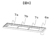
- FIG. 6 is a perspective view of the flow path main body 6a according to the present embodiment.
- the flow passage body 6b is different from the flow passage body 6a in the length in the width direction, but the other structure is basically the same.
- the flow path main unit 6a forms an opening 7a for inserting the power module 1a, an opening 7b for inserting the power module 1b, and an opening 7c for inserting the power module 1c. Do.
- the power modules 1a to 1c are sandwiched by the flow path main portions 6a and 6b.
- the heat dissipation bases of the power modules 1a to 1c are disposed in the openings 7a to 7c of the flow path formers 6a and 6b, respectively.
- edges of the flow path main portions 6a and 6b forming the openings 7a to 7c are welded (for example, laser welding) to the heat dissipation base of the power modules 1a to 1c, respectively. 6a and 6b are integrated.
- the flow path lids 8a and 8b are respectively covered with the flow path body portions 6a and 6b, and the edges of the flow path lids 8a and 8b are welded to the flow path body portions 6a and 6b. Be done.
- FIG. 7 is a cross-sectional view of a power module 1a according to the present embodiment.
- the power modules 1b and 1c have the same configuration and function as the power module 1a.
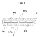
- the power module 1a includes a plurality of power semiconductor elements 25, a plurality of power semiconductor elements 25, and substrates 9a and 9b having a conductive function and an insulating function, and the substrates 9a and 9b, and a heat dissipating base 10a having a heat dissipating function. And 10 b and the resin member 11.
- the resin member 11 seals the plurality of power semiconductor elements 25, the substrates 9a and 9b, and a part of the heat dissipation bases 10a and 10b.
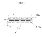
- FIG. 8 is a cross-sectional view for explaining the manufacturing intersection of the power module 1a.
- the dimension A of the heat dissipation base 10a can be manufactured with relatively high accuracy because it is molded by a mold. Since this dimension A is matched with the openings 7a to 7c of the flow path main body 6a with a relatively small tolerance, the side surfaces of the heat dissipation base 10a should be assembled in a state of almost abutting against the inner side surfaces of the openings 7a to 7c. Can.
- FIG.9 and FIG.11 is an expanded sectional view of the opening part 7a periphery of the flow-path main-body part 6a.
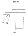
- FIG. 12 is an enlarged cross-sectional view of the vicinity of the opening 7 a of the flow path main body 6 b.
- the side surface 12 of the heat dissipating base 10 a can be brought into abutment with the inner side surface forming the opening 7 a.
- the dimensions B and C shown in FIG. 8 have some tolerance as a result of bonding a plurality of members such as the power semiconductor element 25 and the substrate 9a.
- the tolerance of the dimension B is absorbed by providing the gap 13 between the main surface 26 of the heat dissipation base 10a and the outer surface 27 of the flow path main body 6a shown in FIG.
- the main surface of the heat dissipating base 10 b and the outer surface of the flow passage main portion 6 b are in a butting structure as the contact portion 14. Instead, the tolerance of the dimension C is absorbed by opening the gap 15 between the side surface of the heat dissipating base 10 b and the opening 7 a of the flow path main body 6 b.
- the edge of the opening 7a of the flow passage main portion 6b is obliquely cut so as to be thinner in the direction approaching the heat dissipation base 10b, thereby laser beam 16b for welding. Can be applied from directly below.
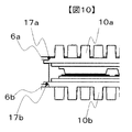
- FIG. 10 is a cross-sectional view of power semiconductor device 1 showing a state after the welding process. Since weld beads 17a and 17b can be provided at positions as shown in FIG. 10, bonding can be performed in a very space-saving manner, so that the power semiconductor device can be miniaturized.
- the power module 1a is already molded by the resin member 11, since the heat affected area can be kept narrow by joining by the laser welding, the resin member 11 is damaged along with the welding. Can be prevented.
- the weld bead 17a has a distance from the resin member 11 in the thickness direction of the heat radiation base 10a, and the weld bead 17b can avoid the influence of heat by separating the distance from the resin member 11 in the horizontal direction.
Landscapes
- Engineering & Computer Science (AREA)
- Power Engineering (AREA)
- Inverter Devices (AREA)
- Cooling Or The Like Of Semiconductors Or Solid State Devices (AREA)
Abstract
パワー半導体装置の小型化を図るとともに信頼性を向上させることである。パワーモジュールの表面に接合される流路の第1開口サイズを第1放熱ベースのサイズと合わせた小さい公差で作成し、裏面に接合される流路の第2開口サイズは表裏放熱ベースの面方向公差を吸収できるように大きく作成する。その上で第1放熱ベースの外側面と第1開口の内側面をほぼ突き当てた形で挿入し、第2放熱ベースはその主面と流路の外面を突き当てた状態で組み立てる。
Description
本発明はパワー半導体装置に関し、特に電気自動車およびハイブリッド自動車への車載用の電力変換装置向けのパワー半導体装置に関する。
電気自動車あるいはハイブリッド自動車においては、車両の動力源としてモータを搭載しており、一般的にモータに供給する電力を制御するために電力変換装置を備えている。
電力変換装置は、IGBT(Insulated Gate Bipolar Transistor)などの電力用半導体素子を内蔵したパワー半導体装置、そのパワー半導体装置を駆動する駆動回路、それらを制御する制御回路、および電流平滑化用のコンデンサを備えている。
特にパワー半導体装置は、電力変換の損失のために大量の熱を発生するため、その冷却構造に対して様々な技術開発がなされてきた。
パワー半導体素子の冷却技術としては空冷が一般的であるが、自動車に関しては水冷技術も広く用いられており、その中でもパワー半導体装置に放熱ベースを直接取り付けて放熱ベースを冷却流路の中に挿入する直接水冷構造は高い冷却性能が得られる。
また、パワー半導体素子の表裏両面から冷却する両面冷却も能力の高い冷却方法であり、それらを組み合わせた両面直接水冷構造も実用化されている。
例えば、特許文献1(特開2010-212412号公報)では、パワー半導体装置の両面に設けられた放熱ベースを冷却流路に挿入する構造が開示されている。本構造案では、片方の面の水の封止を弾性体で行うことによって、パワー半導体装置の表裏の放熱ベースに発生する公差を弾性体の変形によって吸収している。
弾性体の具体例としてはOリング等が考えられるが、Oリングによって封止を行うためにはその周囲に、吸収したい変形量に応じた太さのOリングが収まるOリング溝の幅とOリング溝の両側に必要なスペースが必要であり、ユニットが大きくなってしまうことが課題である。
本発明に係る課題は、パワー半導体装置の小型化を図るとともに信頼性を向上させることである。
本発明に係るパワー半導体装置は、パワー半導体素子を有し当該パワー半導体素子を樹脂部材で封止する回路体と、前記回路体を挟む第1放熱ベース及び第2放熱ベースと、前記回路体を挟んで対向しておりかつ冷媒を流す流路を形成する第1流路形成体及び第2流路形成体と、を備え、前記第1流路形成体は、前記第1放熱ベースに塞がれる第1開口を形成し、前記第2流路形成体は、前記第2放熱ベースに塞がれる第2開口を形成し、前記第1放熱ベース及び前記第2放熱ベースのそれぞれは、主面と、側面と、により形成され、前記第1放熱ベースの前記側面の一部が、前記第1開口の開口空間を形成する前記第1流路形成体の内側面と対向し、前記第2放熱ベースの前記主面の一部が、前記第2開口の周辺を形成する前記第2流路形成体の外面と対向し、前記第1放熱ベースは、当該第1流路形成体の流路側であって当該第1放熱ベースの前記側面及び前記主面を介してと当該第1流路形成体と接合され、前記第2放熱ベースは、当該第2流路形成体の流路側であって当該第2放熱ベースの前記主面のみを介してと当該第2流路形成体と接合される。
本発明により、パワー半導体装置の小型化を図るとともに信頼性を向上させることができる。
本発明の実施形態を説示する前に、本発明の背景を説明する。
省スペースでパワー半導体装置と冷却流路を接合する手段として、例えばレーザ溶接で接合することが考えられる。
レーザ溶接によれば、ビードが細いため非常に省スペースで固定を行うことができる。また、レーザ溶接は、熱が影響する範囲を狭く保てるため、パワー半導体装置に用いられる樹脂部材への影響を小さく抑えることができる。
しかし、ビードが細いことはすなわち、接合時に吸収できる公差(隙間)が狭いので、接合部分は予め精度よく突き当てた状態で組み立てられる必要がある。
ところが、パワー半導体装置は、複数部品をはんだ等で接合して成るため、その表裏の放熱ベースの相対位置はある程度の公差を生じてしまう。具体的には、放熱ベースの位置がちょうど表裏にならず、面に平行方向にずれる面方向の公差と、パワー半導体装置の厚みが設計値からずれる厚さ方向の公差が発生する。
したがって、表裏の冷却流路の開口の構造が同じ場合、放熱ベースを開口に挿入するためには公差分だけ開口を大きく形成し、放熱ベースとの間に隙間を開けておく必要があり、また、厚さ方向にも公差分の隙間が開く。
すると、先に述べたようにレーザ溶接では広い隙間を埋めることができないため、接合が困難になる。
上記のような背景に基づく本発明に係る本実施形態を説明する。
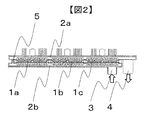
図1は、本実施形態に係るパワー半導体装置1の斜視図である。図2は、図1の平面Aの矢印方向から見たパワー半導体装置の断面図である。
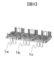
図1に示されるように、パワー半導体装置は、U相交流電流を出力するパワーモジュール1aと、V相交流電流を出力するパワーモジュール1bと、W相交流電流を出力するパワーモジュール1cと、により構成されるインバータ回路を有する。 パワーモジュール1aないし1cは、冷却流路形成体2aと冷却流路形成体2bにより挟まれる。
図2に示されるように、冷却水は、冷却水入口パイプ3より流入し、冷却流路形成体2bを流れながらパワーモジュール1c、パワーモジュール1b、パワーモジュール1aの下側の放熱ベースを通過して冷却する。
その後、冷却水は中間パイプ5を通して冷却流路形成体2aに流れ込む。さらに冷却水は、冷却流路形成体2aを流れながらパワーモジュール1a、パワーモジュール1b、パワーモジュール1cの上側の放熱ベースを通過して冷却し、冷却水出口パイプ4より流出する。
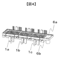
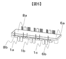
図3は、パワー半導体装置1の組み立て工程のうちパワーモジュール1aないし1cの配置を示す斜視図である。図4は、パワー半導体装置1の組み立て工程のうち流路本体部6a及び6bをパワーモジュール1aないし1cに組み付けた状態を示す斜視図である。図5は、パワー半導体装置1の組み立て工程における完成斜視図である。図6は、本実施形態に係る流路本体部6aの斜視図である。なお流路本体部6bは、流路本体部6aとは幅方向の長さが異なるがその他の構造は基本的に同じである。
図6に示されるように、流路本体部6aは、パワーモジュール1aの挿入する開口部7aと、パワーモジュール1bの挿入する開口部7bと、パワーモジュール1cの挿入する開口部7cと、を形成する。
図4に示されるように、パワーモジュール1aないし1cは、流路本体部6a及び6bにより挟まれる。パワーモジュール1aないし1cのそれぞれの放熱ベースが、流路形成体6a及び6bのそれぞれの開口部7aないし7c内に配置される。
その後、開口部7aないし7cを形成する流路本体部6a及び6bの縁をそれぞれパワーモジュール1aないし1cの放熱ベースに溶接(例えばレーザー溶接)することによって、パワーモジュール1aないし1cと流路本体部6a及び6bが一体化される。
さらに図5に示されるように、流路蓋8a及び8bのそれぞれは、流路本体部6a及び6bのそれぞれに被せられ、流路蓋8a及び8bの縁が流路本体部6a及び6bに溶接される。
図7は、本実施形態に係るパワーモジュール1aの断面図である。なお、パワーモジュール1b及び1cも、パワーモジュール1aと同様な構成及び機能である。
パワーモジュール1aは、複数のパワー半導体素子25と、複数のパワー半導体素子25を挟むとともに導電性機能と絶縁機能を有する基板9a及び9bと、基板9a及び9bを挟むとともに放熱機能を有する放熱ベース10a及び10bと、樹脂部材11と、により構成される。樹脂部材11は、複数のパワー半導体素子25、基板9a及び9bと、放熱ベース10a及び10bの一部を封止する。
図8は、パワーモジュール1aの製造交差を説明するための断面図である。
放熱ベース10aの寸法Aは、型で成形するため、比較的精度よく製造できる。この寸法Aは、比較的小さな公差で流路本体部6aの開口部7aないし7cと一致させられるため、放熱ベース10aの側面は開口部7aないし7cの内側面とほぼ突き当ての状態で組み立てることができる。
この状態を図9、図12及び図13にて説明する。図9及び図11は、流路本体部6aの開口部7a周辺の拡大断面図である。図12は、流路本体部6bの開口部7a周辺の拡大断面図である。
図9及び図11に示されるように、放熱ベース10aの側面12は、開口部7aを形成する内側面と突き当て状態とすることができる。
このとき、図8に示された寸法Bと寸法Cは、パワー半導体素子25や基板9a等の複数の部材を接合した結果として、ある程度の公差を生じる。
そこで、図9に示される放熱ベース10aの主面26と流路本体部6aの外面27との間に隙間13を設けることによって、寸法Bの公差を吸収する。
また、放熱ベース10bの主面と流路本体部6bの外面とは接触部14のように突き当て構造とする。その代わりに、放熱ベース10bの側面と流路本体部6bの開口部7aとの間は隙間15を開けることによって寸法Cの公差を吸収する。
これをレーザ光線16aおよび16bで溶接することによって、冷却流路一体型のパワー半導体装置1を組み立てることができる。
なお、流路本体部6bの開口部7aの縁は、図12の拡大図に示すように、放熱ベース10bに近づく方向に薄くなるように斜めにカットすることによって、溶接のためのレーザ光線16bを真下から当てることができる。
図10は、溶接工程後の状態を示すパワー半導体装置1の断面図である。図10に示されるような位置に溶接ビード17a及び17bを設けることができるため、非常に省スペースでの接合ができるため、パワー半導体装置を小型化することができる。
また、この際、パワーモジュール1aは既に樹脂部材11によってモールドされているが、レーザ溶接で接合することで熱影響領域を狭く保つことができるため、溶接に伴って樹脂部材11に損傷を与えることを防止できる。溶接ビード17aは、放熱ベース10aの厚さ方向に樹脂部材11からの距離をとっており、溶接ビード17bは水平方向に樹脂部材11から距離を離すことによって熱の影響を避けることができる。
1…パワー半導体装置、1a~1c…パワーモジュール、2a及び2b…冷却流路形成体、3…冷却水入口パイプ、4…冷却水出口パイプ、5…中間パイプ、6a及び6b…流路本体部、7aないし7c…開口部、8a及び8b…流路蓋、9a及び9b…基板、10a及び10b…放熱ベース、11…樹脂部材、12…放熱ベース10aの側面、13…隙間
、14…接触部、15…隙間、16a及び16b…レーザ光線、17a及び17b…溶接ビード、25…パワー半導体素子、26…放熱ベース10aの主面、27…流路本体部6aの外面
、14…接触部、15…隙間、16a及び16b…レーザ光線、17a及び17b…溶接ビード、25…パワー半導体素子、26…放熱ベース10aの主面、27…流路本体部6aの外面
Claims (3)
- パワー半導体素子を有し当該パワー半導体素子を樹脂部材で封止する回路体と、
前記回路体を挟む第1放熱ベース及び第2放熱ベースと、
前記回路体を挟んで対向しておりかつ冷媒を流す流路を形成する第1流路形成体及び第2流路形成体と、を備え、
前記第1流路形成体は、前記第1放熱ベースに塞がれる第1開口を形成し、
前記第2流路形成体は、前記第2放熱ベースに塞がれる第2開口を形成し、
前記第1放熱ベース及び前記第2放熱ベースのそれぞれは、主面と、側面と、により形成され、
前記第1放熱ベースの前記側面の一部が、前記第1開口の開口空間を形成する前記第1流路形成体の内側面と対向し、
前記第2放熱ベースの前記主面の一部が、前記第2開口の周辺を形成する前記第2流路形成体の外面と対向し、
前記第1放熱ベースは、当該第1流路形成体の流路側であって当該第1放熱ベースの前記側面及び前記主面を介してと当該第1流路形成体と接合され、
前記第2放熱ベースは、当該第2流路形成体の流路側であって当該第2放熱ベースの前記主面のみを介してと当該第2流路形成体と接合されるパワー半導体装置。 - 請求項1に記載のパワー半導体装置において、
前記第1放熱ベースと前記第1流路形成体の接合部には金属溶融部が形成され、
前記第2放熱ベースと前記第2流路形成体の接合部には金属溶融部が形成されるパワー半導体装置。 - 請求項1または2に記載のパワー半導体装置において、
前記第2流路形成体は、前記第2開口部が前記第2放熱ベースに向う方向に沿って薄くなるように形成されるパワー半導体装置。
Applications Claiming Priority (2)
| Application Number | Priority Date | Filing Date | Title |
|---|---|---|---|
| JP2017189402A JP6847013B2 (ja) | 2017-09-29 | 2017-09-29 | パワー半導体装置 |
| JP2017-189402 | 2017-09-29 |
Publications (1)
| Publication Number | Publication Date |
|---|---|
| WO2019064873A1 true WO2019064873A1 (ja) | 2019-04-04 |
Family
ID=65902888
Family Applications (1)
| Application Number | Title | Priority Date | Filing Date |
|---|---|---|---|
| PCT/JP2018/028187 Ceased WO2019064873A1 (ja) | 2017-09-29 | 2018-07-27 | パワー半導体装置 |
Country Status (2)
| Country | Link |
|---|---|
| JP (1) | JP6847013B2 (ja) |
| WO (1) | WO2019064873A1 (ja) |
Cited By (1)
| Publication number | Priority date | Publication date | Assignee | Title |
|---|---|---|---|---|
| US10950520B2 (en) * | 2018-11-22 | 2021-03-16 | Siliconware Precision Industries Co., Ltd. | Electronic package, method for fabricating the same, and heat dissipator |
Families Citing this family (3)
| Publication number | Priority date | Publication date | Assignee | Title |
|---|---|---|---|---|
| DE112022004973T5 (de) | 2021-10-15 | 2024-08-14 | Denso Corporation | Stromumwandlungsvorrichtung |
| JP2024093781A (ja) * | 2022-12-27 | 2024-07-09 | 株式会社デンソー | 電力変換装置 |
| JP2025172531A (ja) * | 2024-05-13 | 2025-11-26 | 株式会社デンソー | 端子台 |
Citations (2)
| Publication number | Priority date | Publication date | Assignee | Title |
|---|---|---|---|---|
| JP2012257369A (ja) * | 2011-06-08 | 2012-12-27 | Hitachi Automotive Systems Ltd | パワーモジュールおよびそれを用いた電力変換装置 |
| JP2017011923A (ja) * | 2015-06-24 | 2017-01-12 | トヨタ自動車株式会社 | 電力変換装置 |
-
2017
- 2017-09-29 JP JP2017189402A patent/JP6847013B2/ja active Active
-
2018
- 2018-07-27 WO PCT/JP2018/028187 patent/WO2019064873A1/ja not_active Ceased
Patent Citations (2)
| Publication number | Priority date | Publication date | Assignee | Title |
|---|---|---|---|---|
| JP2012257369A (ja) * | 2011-06-08 | 2012-12-27 | Hitachi Automotive Systems Ltd | パワーモジュールおよびそれを用いた電力変換装置 |
| JP2017011923A (ja) * | 2015-06-24 | 2017-01-12 | トヨタ自動車株式会社 | 電力変換装置 |
Cited By (1)
| Publication number | Priority date | Publication date | Assignee | Title |
|---|---|---|---|---|
| US10950520B2 (en) * | 2018-11-22 | 2021-03-16 | Siliconware Precision Industries Co., Ltd. | Electronic package, method for fabricating the same, and heat dissipator |
Also Published As
| Publication number | Publication date |
|---|---|
| JP2019068533A (ja) | 2019-04-25 |
| JP6847013B2 (ja) | 2021-03-24 |
Similar Documents
| Publication | Publication Date | Title |
|---|---|---|
| US8248809B2 (en) | Inverter power module with distributed support for direct substrate cooling | |
| JP6847013B2 (ja) | パワー半導体装置 | |
| EP4135498B1 (en) | Encapsulation structure and encapsulation method of power module | |
| JP6161713B2 (ja) | 電力変換装置 | |
| JP5642022B2 (ja) | 半導体装置および半導体装置の製造方法 | |
| JP5691916B2 (ja) | 電力変換装置 | |
| JP2017199829A (ja) | パワーモジュール構造 | |
| JP6286039B2 (ja) | パワー半導体モジュールおよびパワー半導体モジュールの製造方法 | |
| WO2016076040A1 (ja) | 電力変換装置 | |
| JP6899784B2 (ja) | パワー半導体装置 | |
| WO2019003718A1 (ja) | パワー半導体装置及びそれを用いた電力変換装置 | |
| JP2015076932A (ja) | 電力変換装置 | |
| JP2011182632A (ja) | 電力変換装置 | |
| TWI818106B (zh) | 散熱器、冷卻裝置 | |
| JP5333357B2 (ja) | 半導体モジュールの積層体 | |
| WO2004105219A1 (ja) | リニアモータ電機子およびこれを用いたリニアモータ | |
| JP6588154B2 (ja) | ケース、半導体装置、ケースの製造方法 | |
| JP7532530B2 (ja) | 電力変換装置、電力変換装置の製造方法 | |
| JP7091893B2 (ja) | 半導体モジュールの積層体及びその製造方法 | |
| JP5899962B2 (ja) | 半導体モジュール及び電力変換装置 | |
| JP2022188312A (ja) | パワーモジュールおよびパワーモジュールの製造方法 | |
| KR102924256B1 (ko) | 파워 모듈 냉각 장치 및 파워 모듈 냉각 장치의 제조 방법 | |
| JP2012138395A (ja) | 冷却器のロウ付け構造 | |
| CN118355488A (zh) | 半导体装置及绝缘构件 | |
| WO2025083789A1 (ja) | 半導体モジュールの製造方法、半導体モジュール |
Legal Events
| Date | Code | Title | Description |
|---|---|---|---|
| 121 | Ep: the epo has been informed by wipo that ep was designated in this application |
Ref document number: 18862687 Country of ref document: EP Kind code of ref document: A1 |
|
| NENP | Non-entry into the national phase |
Ref country code: DE |
|
| 122 | Ep: pct application non-entry in european phase |
Ref document number: 18862687 Country of ref document: EP Kind code of ref document: A1 |