WO2019059074A1 - レジストパターン形成方法及び基板の処理方法 - Google Patents
レジストパターン形成方法及び基板の処理方法 Download PDFInfo
- Publication number
- WO2019059074A1 WO2019059074A1 PCT/JP2018/033892 JP2018033892W WO2019059074A1 WO 2019059074 A1 WO2019059074 A1 WO 2019059074A1 JP 2018033892 W JP2018033892 W JP 2018033892W WO 2019059074 A1 WO2019059074 A1 WO 2019059074A1
- Authority
- WO
- WIPO (PCT)
- Prior art keywords
- substrate
- contact
- metal
- resist pattern
- exposure
- Prior art date
- Legal status (The legal status is an assumption and is not a legal conclusion. Google has not performed a legal analysis and makes no representation as to the accuracy of the status listed.)
- Ceased
Links
Classifications
-
- G—PHYSICS
- G03—PHOTOGRAPHY; CINEMATOGRAPHY; ANALOGOUS TECHNIQUES USING WAVES OTHER THAN OPTICAL WAVES; ELECTROGRAPHY; HOLOGRAPHY
- G03F—PHOTOMECHANICAL PRODUCTION OF TEXTURED OR PATTERNED SURFACES, e.g. FOR PRINTING, FOR PROCESSING OF SEMICONDUCTOR DEVICES; MATERIALS THEREFOR; ORIGINALS THEREFOR; APPARATUS SPECIALLY ADAPTED THEREFOR
- G03F7/00—Photomechanical, e.g. photolithographic, production of textured or patterned surfaces, e.g. printing surfaces; Materials therefor, e.g. comprising photoresists; Apparatus specially adapted therefor
- G03F7/70—Microphotolithographic exposure; Apparatus therefor
- G03F7/70008—Production of exposure light, i.e. light sources
- G03F7/70033—Production of exposure light, i.e. light sources by plasma extreme ultraviolet [EUV] sources
-
- G—PHYSICS
- G03—PHOTOGRAPHY; CINEMATOGRAPHY; ANALOGOUS TECHNIQUES USING WAVES OTHER THAN OPTICAL WAVES; ELECTROGRAPHY; HOLOGRAPHY
- G03F—PHOTOMECHANICAL PRODUCTION OF TEXTURED OR PATTERNED SURFACES, e.g. FOR PRINTING, FOR PROCESSING OF SEMICONDUCTOR DEVICES; MATERIALS THEREFOR; ORIGINALS THEREFOR; APPARATUS SPECIALLY ADAPTED THEREFOR
- G03F7/00—Photomechanical, e.g. photolithographic, production of textured or patterned surfaces, e.g. printing surfaces; Materials therefor, e.g. comprising photoresists; Apparatus specially adapted therefor
- G03F7/004—Photosensitive materials
- G03F7/09—Photosensitive materials characterised by structural details, e.g. supports, auxiliary layers
- G03F7/091—Photosensitive materials characterised by structural details, e.g. supports, auxiliary layers characterised by antireflection means or light filtering or absorbing means, e.g. anti-halation, contrast enhancement
-
- G—PHYSICS
- G03—PHOTOGRAPHY; CINEMATOGRAPHY; ANALOGOUS TECHNIQUES USING WAVES OTHER THAN OPTICAL WAVES; ELECTROGRAPHY; HOLOGRAPHY
- G03F—PHOTOMECHANICAL PRODUCTION OF TEXTURED OR PATTERNED SURFACES, e.g. FOR PRINTING, FOR PROCESSING OF SEMICONDUCTOR DEVICES; MATERIALS THEREFOR; ORIGINALS THEREFOR; APPARATUS SPECIALLY ADAPTED THEREFOR
- G03F7/00—Photomechanical, e.g. photolithographic, production of textured or patterned surfaces, e.g. printing surfaces; Materials therefor, e.g. comprising photoresists; Apparatus specially adapted therefor
- G03F7/004—Photosensitive materials
- G03F7/0042—Photosensitive materials with inorganic or organometallic light-sensitive compounds not otherwise provided for, e.g. inorganic resists
- G03F7/0043—Chalcogenides; Silicon, germanium, arsenic or derivatives thereof; Metals, oxides or alloys thereof
-
- G—PHYSICS
- G03—PHOTOGRAPHY; CINEMATOGRAPHY; ANALOGOUS TECHNIQUES USING WAVES OTHER THAN OPTICAL WAVES; ELECTROGRAPHY; HOLOGRAPHY
- G03F—PHOTOMECHANICAL PRODUCTION OF TEXTURED OR PATTERNED SURFACES, e.g. FOR PRINTING, FOR PROCESSING OF SEMICONDUCTOR DEVICES; MATERIALS THEREFOR; ORIGINALS THEREFOR; APPARATUS SPECIALLY ADAPTED THEREFOR
- G03F7/00—Photomechanical, e.g. photolithographic, production of textured or patterned surfaces, e.g. printing surfaces; Materials therefor, e.g. comprising photoresists; Apparatus specially adapted therefor
- G03F7/16—Coating processes; Apparatus therefor
-
- G—PHYSICS
- G03—PHOTOGRAPHY; CINEMATOGRAPHY; ANALOGOUS TECHNIQUES USING WAVES OTHER THAN OPTICAL WAVES; ELECTROGRAPHY; HOLOGRAPHY
- G03F—PHOTOMECHANICAL PRODUCTION OF TEXTURED OR PATTERNED SURFACES, e.g. FOR PRINTING, FOR PROCESSING OF SEMICONDUCTOR DEVICES; MATERIALS THEREFOR; ORIGINALS THEREFOR; APPARATUS SPECIALLY ADAPTED THEREFOR
- G03F7/00—Photomechanical, e.g. photolithographic, production of textured or patterned surfaces, e.g. printing surfaces; Materials therefor, e.g. comprising photoresists; Apparatus specially adapted therefor
- G03F7/16—Coating processes; Apparatus therefor
- G03F7/162—Coating on a rotating support, e.g. using a whirler or a spinner
-
- G—PHYSICS
- G03—PHOTOGRAPHY; CINEMATOGRAPHY; ANALOGOUS TECHNIQUES USING WAVES OTHER THAN OPTICAL WAVES; ELECTROGRAPHY; HOLOGRAPHY
- G03F—PHOTOMECHANICAL PRODUCTION OF TEXTURED OR PATTERNED SURFACES, e.g. FOR PRINTING, FOR PROCESSING OF SEMICONDUCTOR DEVICES; MATERIALS THEREFOR; ORIGINALS THEREFOR; APPARATUS SPECIALLY ADAPTED THEREFOR
- G03F7/00—Photomechanical, e.g. photolithographic, production of textured or patterned surfaces, e.g. printing surfaces; Materials therefor, e.g. comprising photoresists; Apparatus specially adapted therefor
- G03F7/20—Exposure; Apparatus therefor
- G03F7/2002—Exposure; Apparatus therefor with visible light or UV light, through an original having an opaque pattern on a transparent support, e.g. film printing, projection printing; by reflection of visible or UV light from an original such as a printed image
- G03F7/2004—Exposure; Apparatus therefor with visible light or UV light, through an original having an opaque pattern on a transparent support, e.g. film printing, projection printing; by reflection of visible or UV light from an original such as a printed image characterised by the use of a particular light source, e.g. fluorescent lamps or deep UV light
-
- G—PHYSICS
- G03—PHOTOGRAPHY; CINEMATOGRAPHY; ANALOGOUS TECHNIQUES USING WAVES OTHER THAN OPTICAL WAVES; ELECTROGRAPHY; HOLOGRAPHY
- G03F—PHOTOMECHANICAL PRODUCTION OF TEXTURED OR PATTERNED SURFACES, e.g. FOR PRINTING, FOR PROCESSING OF SEMICONDUCTOR DEVICES; MATERIALS THEREFOR; ORIGINALS THEREFOR; APPARATUS SPECIALLY ADAPTED THEREFOR
- G03F7/00—Photomechanical, e.g. photolithographic, production of textured or patterned surfaces, e.g. printing surfaces; Materials therefor, e.g. comprising photoresists; Apparatus specially adapted therefor
- G03F7/26—Processing photosensitive materials; Apparatus therefor
- G03F7/30—Imagewise removal using liquid means
-
- H—ELECTRICITY
- H10—SEMICONDUCTOR DEVICES; ELECTRIC SOLID-STATE DEVICES NOT OTHERWISE PROVIDED FOR
- H10P—GENERIC PROCESSES OR APPARATUS FOR THE MANUFACTURE OR TREATMENT OF DEVICES COVERED BY CLASS H10
- H10P50/00—Etching of wafers, substrates or parts of devices
- H10P50/71—Etching of wafers, substrates or parts of devices using masks for conductive or resistive materials
-
- H—ELECTRICITY
- H10—SEMICONDUCTOR DEVICES; ELECTRIC SOLID-STATE DEVICES NOT OTHERWISE PROVIDED FOR
- H10P—GENERIC PROCESSES OR APPARATUS FOR THE MANUFACTURE OR TREATMENT OF DEVICES COVERED BY CLASS H10
- H10P76/00—Manufacture or treatment of masks on semiconductor bodies, e.g. by lithography or photolithography
Definitions
- the present invention relates to a method of forming a resist pattern and a method of processing a substrate.
- a resist process is used in which a resist film laminated on a substrate is exposed and developed, and the obtained resist pattern is used as a mask to etch the substrate (Japanese Patent Laid-Open No. 2004-310019) And WO 2012/039337).
- exposure light used is KrF excimer laser light (248 nm) and ArF excimer laser light (193 nm), extreme ultraviolet (13.5 nm, EUV), electron beam (EB) Tends to be shortened.
- the present invention has been made based on the circumstances as described above, and an object thereof is to provide a method of forming a resist pattern and a method of processing a substrate with high sensitivity and excellent resolution.
- Invention made in order to solve the above-mentioned subject is the exposure of the ultraviolet rays to the surface containing the above-mentioned metallic element of the substrate containing the metallic element in at least one surface, the exposure of plasma, the contact of water, the contact of alkaline, acid
- Another invention made to solve the above-mentioned problems is a method of processing a substrate which is used to form a resist pattern by exposure to extreme ultraviolet light or an electron beam, and which contains a metal element in at least one surface layer. Treatment of one or more of the following: exposure of ultraviolet light to the surface of the substrate containing the metal element, exposure of plasma, contact of water, contact of alkali, contact of acid, contact of hydrogen peroxide and contact of ozone
- a substrate processing method comprising the steps of:
- the method for forming a resist pattern and the method for treating a substrate of the present invention it is possible to obtain a resist pattern with high sensitivity and excellent resolution. Therefore, they can be suitably used for extreme ultraviolet or electron beam lithography, and can be suitably used for the manufacture of semiconductor devices etc. for which further miniaturization is expected to progress in the future.
- the method for forming a resist pattern comprises the steps of preparing a substrate containing a metal element in at least one surface layer (hereinafter also referred to as “preparation step”), exposing ultraviolet light to the surface containing the metal element of the substrate, and plasma A step of performing one or more treatments of exposure of water, contact of alkali, contact of alkali, contact of acid, contact of hydrogen peroxide and contact of ozone (hereinafter, also referred to as “treatment step”), and the above treatment A step of applying a resist composition on the surface treated in the step (hereinafter, also referred to as a “coating step”) and a step of exposing the resist film formed in the coating step with extreme ultraviolet light or an electron beam And an “exposure step”), and a step of developing the exposed resist film (hereinafter, also referred to as “development step”). Further, the resist pattern forming method may include a step of etching the substrate using the resist pattern formed in the developing step as a mask
- the said resist pattern formation method can form the resist pattern which is excellent in resolution with high sensitivity by including said each process.
- the reason why the resist pattern forming method of the present invention has the above-described configuration is not necessarily clear. However, for example, it can be inferred as follows. That is, when a substrate containing a metal element on the surface is used, in the extreme ultraviolet or electron beam lithography, the irradiated extreme ultraviolet or electron beam is absorbed by the metal element on the substrate surface to generate secondary electrons etc. It is considered that the secondary electrons contribute to the sensitivity in the resist film. According to the resist pattern forming method, by performing exposure and / or contact in the processing step, the electronic state, coordination state, etc.
- a substrate (hereinafter, also referred to as a “substrate (P)”) containing a metal element in at least one surface layer is prepared.
- “Surface” means the region from the surface of the substrate to a depth of 5 nm.
- the substrate (P) examples include a metal-containing substrate and a substrate having a layer containing a metal element (a) on at least one surface side (hereinafter, also referred to as a “metal-containing layer (T)”).
- a patterned substrate such as a wiring trench (trench) or a plug trench (via) may be used.
- the metal-containing substrate is, for example, a titanium-containing substrate, a titanium-oxide-containing substrate, a titanium-containing substrate such as a titanium nitride-containing substrate, a zirconium oxide-containing substrate, a zirconium-containing substrate such as Zr-containing substrate, a hafnium oxide-containing substrate or the like
- the metal-containing layer (T) is a coating of a metal-containing composition (hereinafter also referred to as “metal-containing composition (X)”), a chemical vapor deposition (CVD) method, a physical vapor deposition (PVD) method, atomic layer deposition It can be formed by the (ALD) method or the like.
- metal-containing composition hereinafter also referred to as “metal-containing composition (X)”
- CVD chemical vapor deposition
- PVD physical vapor deposition
- ALD atomic layer deposition
- the coating film formed by the coating of the metal-containing composition (X) may be heat treated.
- 90 ° C is preferred and 150 ° C is more preferred.
- 550 ° C is preferred and 300 ° C is more preferred.
- the lower limit of the average thickness of the metal-containing layer (T) to be formed is preferably 1 nm, and more preferably 3 nm.
- 50 nm is preferred, and 30 nm is more preferred.
- CVD method plasma-assisted CVD method, a low pressure CVD method, etc. are mentioned, for example.
- PVD method a sputtering method, an evaporation method, etc. are mentioned, for example.
- metal containing layer (T) formed by CVD method, PVD method, ALD method etc. a titanium oxide film, a titanium nitride film, a zirconium oxide film, an aluminum oxide film, an aluminum oxynitride film, a hafnium oxide film etc. are mentioned, for example Be
- the substrate of the substrate having the metal-containing layer (T) examples include a substrate having an insulating film such as silicon oxide, silicon nitride, silicon oxynitride, or polysiloxane, a resin substrate, and the like.
- a substrate having an insulating film such as silicon oxide, silicon nitride, silicon oxynitride, or polysiloxane
- a resin substrate and the like.
- a coated silicon wafer or the like can be used as the substrate having the metal-containing layer (T).
- metal element (a) examples include, for example, metal elements belonging to the third to seventh periods of Groups 3 to 15 of the periodic table Can be mentioned.
- the metal element (a) does not include metalloid elements such as boron, silicon, and arsenic.
- Examples of the group 3 metal element (a) include scandium, yttrium, lanthanum, cerium and the like.
- Examples of the metal element (a) of group 4 include titanium, zirconium, hafnium and the like,
- Examples of the group 5 metal element (a) include vanadium, niobium, tantalum and the like,
- Examples of the group 6 metal element (a) include chromium, molybdenum, tungsten, etc.
- Examples of the metal element (a) of group 7 include manganese, rhenium and the like,
- Examples of the metal element (a) of group 8 include iron, ruthenium, osmium, etc.
- Examples of the group 9 metal element (a) include cobalt, rhodium, iridium and the like.
- Examples of the group 10 metal element (a) include nickel, palladium, platinum and the like, Copper, silver, gold and the like as the group 11 metal element (a), Zinc, cadmium, mercury and the like as the metal element (a) of Group 12
- Examples of the group 13 metal element (a) aluminum, gallium, indium and the like, Germanium, tin, lead and the like can be used as the group 14 metal element (a)
- Examples of the group 15 metal element (a) include antimony and bismuth.
- the metal element (a) is preferably a metal element belonging to the fourth to seventh periods of the third to fifteenth groups, and a metal element belonging to the fourth to seventh periods of the fourth to sixth groups. More preferably, metal elements belonging to Group 4 are more preferred, and titanium or zirconium is particularly preferred.
- the metal-containing composition (X) has, for example, a composition containing a compound having a metal-oxygen covalent bond (hereinafter, also referred to as “[A] compound”) and a solvent (hereinafter, also referred to as “[B] solvent”) Things etc.
- the compound may contain a metal element (a) and another element other than oxygen.
- Other elements include, for example, metalloid elements such as boron and silicon, and nonmetal elements such as carbon, hydrogen, nitrogen, phosphorus, sulfur and halogen. Among these, carbon and / or hydrogen are preferred.
- the lower limit of the content of the metal element (a) in the compound (A) is preferably 10% by mass, more preferably 20% by mass, and still more preferably 30% by mass. As a maximum of the above-mentioned content rate, 50 mass% is preferred.
- the atomic content of the metal element (a) can be determined by measurement using a differential thermal balance (TG / DTA).
- Examples of the compound [A] include polynuclear complexes having a metal-oxygen-metal bond.
- the "polynuclear complex” refers to a complex having a plurality of metal atoms. Such a polynuclear complex can be synthesized, for example, by hydrolysis and condensation of a metal-containing compound having a hydrolyzable group, as described later.
- the lower limit of the polystyrene equivalent weight average molecular weight (Mw) of the [A] compound by gel permeation chromatography (GPC) is preferably 1,000, more preferably 1,500. , 2,000 is more preferred.
- Mw polystyrene equivalent weight average molecular weight
- 10,000 are preferable, 8,000 are more preferable, and 6,000 are more preferable.
- the Mw of the [A] compound is measured using a GPC column (two “AWM-H”, one “AW-H” and two “AW2500” of Toso Co., Ltd.), and the flow rate: 0 .3 mL / min, elution solvent: N, N'-dimethylacetamide to which LiBr (30 mM) and citric acid (30 mM) were added, column temperature: gel perm at standard conditions of 40 ° C. using monodispersed polystyrene as standard It is a value measured by an ion chromatography (detector: differential refractometer).
- the lower limit of the content of the compound [A] is preferably 70% by mass, more preferably 80% by mass, and still more preferably 90% by mass, relative to the total solid content of the metal-containing composition (X).
- the upper limit of the content may be 100% by mass.
- a commercially available metal compound can also be used as the compound [A], for example, using a metal-containing compound having a hydrolyzable group (hereinafter, also referred to as “[b] metal-containing compound”), a hydrolysis condensation reaction can be performed It can be synthesized by the method to be performed. That is, the [A] compound can be derived from the [b] metal-containing compound.
- “hydrolytic condensation reaction” means that the hydrolyzable group possessed by the [b] metal-containing compound is hydrolyzed and converted to —OH, and the resulting two —OHs are dehydrated and condensed to form —O— Refers to the reaction that is formed.
- the metal-containing compound is a metal compound having a hydrolyzable group (hereinafter also referred to as "metal compound (I)"), a hydrolyzate of metal compound (I), a hydrolysis condensate of metal compound (I) Or a combination of these.
- metal compounds (I) can be used singly or in combination of two or more.
- hydrolysable group a halogen atom, an alkoxy group, an acyloxy group etc. are mentioned, for example.
- halogen atom a fluorine atom, a chlorine atom, a bromine atom, an iodine atom etc. are mentioned, for example.
- alkoxy group examples include a methoxy group, an ethoxy group, an n-propoxy group, an isopropoxy group and a butoxy group.
- acyloxy group examples include acetoxy group, ethyryloxy group, propionyloxy group, butyryloxy group, t-butyryloxy group, t-amylyloxy group, n-hexane carbonyloxy group, n-octane carbonyloxy group and the like.
- the hydrolyzable group is preferably an alkoxy group, more preferably an isopropoxy group or a butoxy group.
- the hydrolytic condensate of metal compound (I) is a metal element (a) as long as the effects of the present invention are not impaired.
- a hydrolytic condensate of the metal compound (I) containing the compound of formula (I) and the compound containing the metalloid element may be contained in the hydrolysis condensate of metal compound (I) in the range which does not impair the effect of the present invention. Examples of such metalloid elements include boron, silicon, arsenic, and tellurium.
- the content of metalloid atoms in the hydrolysis condensate of metal compound (I) is usually less than 50 at% with respect to the total of the atoms of metal element (a) and metalloid atoms in the hydrolysis condensate, 30 atomic% or less is preferable and 10 atomic% or less is more preferable.
- metal compound (I) examples include a compound represented by the following formula (1) (hereinafter, also referred to as “metal compound (I-1)”) and the like.
- M is a metal atom.
- L is a ligand.
- a is an integer of 0 to 6; When a is 2 or more, a plurality of L's are the same as or different from each other.
- Y is a hydrolyzable group selected from a halogen atom, an alkoxy group and an acyloxy group.
- b is an integer of 2 to 6; The plurality of Y's are the same as or different from one another.
- L is a ligand which does not correspond to Y.
- Examples of the metal atom represented by M include the same atoms as those exemplified as the atom of the metal element (a) contained in the surface layer of the substrate (P).
- a monodentate ligand and a polydentate ligand are mentioned.
- Examples of the monodentate ligand include hydroxo ligands, carboxy ligands, amido ligands, amine ligands, ammonia ligands, olefin ligands and the like.
- amido ligand for example, unsubstituted amido ligand (NH 2 ), methyl amido ligand (NH Me), dimethyl amido ligand (NMe 2 ), diethyl amido ligand (NEt 2 ), dipropyl amide ligand (NPr 2), and the like.
- amine ligand As an amine ligand, a pyridine ligand, a trimethylamine ligand, a piperidine ligand etc. are mentioned, for example.
- olefin ligand examples include linear olefins such as ethylene and propylene, and cyclic olefins such as cyclopentene, cyclohexene and norbornene.
- polydentate ligand examples include a ligand derived from a hydroxy acid ester, a ligand derived from a ⁇ -diketone, a ligand derived from a ⁇ -ketoester, a ligand derived from an ⁇ , ⁇ -dicarboxylic acid ester, Examples thereof include hydrocarbons having a plurality of ⁇ bonds, diphosphines and the like.
- hydroxy acid ester examples include glycolic acid ester, lactic acid ester, 2-hydroxycyclohexane-1-carboxylic acid ester, salicylic acid ester and the like.
- Examples of the ⁇ -diketones include 2,4-pentanedione, 3-methyl-2,4-pentanedione, 3-ethyl-2,4-pentanedione and the like.
- ⁇ -ketoester examples include acetoacetic acid ester, ⁇ -alkyl substituted acetoacetic acid ester, ⁇ -ketopentanoic acid ester, benzoylacetic acid ester, 1,3-acetonedicarboxylic acid ester and the like.
- Examples of the ⁇ , ⁇ -dicarboxylic acid esters include malonic acid diesters, ⁇ -alkyl-substituted malonic acid diesters, ⁇ -cycloalkyl-substituted malonic acid diesters, and ⁇ -aryl-substituted malonic acid diesters.
- hydrocarbon having a plurality of ⁇ bonds examples include chain dienes such as butadiene and isoprene, cyclic dienes such as cyclopentadiene, methylcyclopentadiene, pentamethylcyclopentadiene, cyclohexadiene, norbornadiene and the like, benzene, toluene, xylene, hexa Aromatic hydrocarbons such as methylbenzene, naphthalene and indene can be mentioned.
- chain dienes such as butadiene and isoprene
- cyclic dienes such as cyclopentadiene, methylcyclopentadiene, pentamethylcyclopentadiene, cyclohexadiene, norbornadiene and the like
- benzene toluene
- xylene hexa
- Aromatic hydrocarbons such as methylbenzene, naphthalene and indene can be mentioned.
- diphosphine examples include 1,1-bis (diphenylphosphino) methane, 1,2-bis (diphenylphosphino) ethane, 1,3-bis (diphenylphosphino) propane, and 2,2′-bis (diphenyl).
- diphosphine examples include phosphino) -1,1'-binaphthyl, 1,1'-bis (diphenylphosphino) ferrocene and the like.
- 0 to 3 is preferable, 0 to 2 is more preferable, 1 or 2 is more preferable, and 2 is particularly preferable.
- hydrolysable group represented by Y As a hydrolysable group represented by Y, the group similar to the group illustrated as a hydrolysable group of said [b] metal containing compound, etc. are mentioned, for example.
- the molecular weight of the hydrolytic condensation product [A] compound can be increased appropriately, whereby the sensitivity in the resist pattern formation method can be further improved.
- the metal-containing compound is preferably a metal alkoxide which is neither hydrolyzed nor hydrolyzed and condensed, and a metal alkoxide which has a ligand and is neither hydrolyzed nor hydrolyzed and condensed.
- the metal-containing compound for example, as a compound containing titanium, diisopropoxybis (2,4-pentanedionate) titanium (IV), tetra n-butoxy titanium (IV), tetra n-propoxy titanium (IV ), Tri-n-butoxy monostearate titanium (IV), titanium (IV) butoxide oligomer, aminopropyl trimethoxy titanium (IV), triethoxy mono (2,4-pentanedionate) titanium (IV), tri n- Propoxymono (2,4-pentanedionate) titanium (IV), triisopropoxymono (2,4-pentanedionate) titanium, di n-butoxybis (2,4-pentanedionate) titanium (IV), etc.
- Examples of compounds containing zirconium include dibutoxybis (ethylacetoacetate) zirconium (IV), di n-butoxybis (2,4-pentanedionate) zirconium (IV), tetra n-butoxyzirconium (IV), tetra n-propoxyzirconium ( IV), tetraisopropoxyzirconium (IV), aminopropyltriethoxyzirconium (IV), 2- (3,4-epoxycyclohexyl) ethyltrimethoxyzirconium (IV), ⁇ -glycidoxypropyltrimethoxyzirconium (IV) , 3-isocyanopropyltrimethoxyzirconium (IV), triethoxymono (2,4-pentanedionate) zirconium (IV), tri-n-propoxymono (2,4-pentanedionate) zirconium (IV) , Triisopropoxy mono (2,
- Examples of compounds containing cobalt include dichloro [ethylenebis (diphenylphosphine)] cobalt (II), As compounds containing zinc, diisopropoxy zinc (II), zinc acetate (II) and the like, As compounds containing indium, indium acetate (III), triisopropoxy indium (III), etc.
- Examples of compounds containing tin include tetraethyldiacetoxystannoxane, tetrabutoxytin (IV), tetraisopropoxytin (IV), t-butyltris (diethylamido) tin (IV), etc.
- Examples of compounds containing germanium include tetraisopropoxygermanium (IV).
- a compound capable of becoming a monodentate ligand or a polydentate ligand a compound capable of becoming a crosslinking ligand, etc. are added in addition to the metal compound (I) in the synthesis reaction of the compound You may As a compound which can become said bridge
- Examples of the method of carrying out a hydrolysis condensation reaction using the metal-containing compound (b) include a method of subjecting a metal-containing compound (b) to a hydrolysis condensation reaction in a solvent containing water.
- a metal-containing compound (b) may be added as necessary.
- the lower limit of the amount of water used for this hydrolytic condensation reaction is preferably 0.2 moles, more preferably 1 mole, and 3 moles with respect to the hydrolyzable group possessed by the [b] metal-containing compound etc. More preferable.
- the upper limit of the amount of water is preferably 20 moles, more preferably 15 moles, and still more preferably 10 moles.
- solvent used for synthetic reaction of [A] compound it does not specifically limit as a solvent used for synthetic reaction of [A] compound,
- the solvent similar to what is illustrated as a [B] solvent mentioned later can be used.
- ester solvents, alcohol solvents and / or ether solvents are preferable, alcohol solvents and / or ether solvents are more preferable, ether solvents having a glycol structure are more preferable, propylene glycol monomethyl ether and And / or propylene glycol monoethyl ether is particularly preferred.
- the used solvent may be removed after the reaction, but it may be used as the solvent of the metal-containing composition (X) as it is without removal after the reaction.
- the lower limit of the temperature for the synthesis reaction of the compound is preferably 0 ° C, more preferably 10 ° C. As a maximum of the above-mentioned temperature, 150 ° C is preferred and 100 ° C is more preferred.
- the lower limit of the synthesis reaction time of the compound is preferably 1 minute, more preferably 10 minutes, and still more preferably 1 hour.
- the upper limit of the time is preferably 100 hours, more preferably 50 hours, and still more preferably 10 hours.
- the solvent is not particularly limited as long as it can dissolve or disperse the [A] compound and other components contained as needed.
- examples of the solvent [B] include alcohol solvents, ketone solvents, ether solvents, ester solvents, nitrogen-containing solvents, water and the like.
- a solvent can be used individually by 1 type or in combination of 2 or more types.
- alcohol solvents examples include monoalcohol solvents such as methanol, ethanol, n-propanol, isopropanol, n-butanol and isobutanol; and polyhydric alcohols such as ethylene glycol, 1,2-propylene glycol, diethylene glycol and dipropylene glycol. A system solvent etc. are mentioned.
- ketone solvents include acetone, methyl ethyl ketone, methyl-n-propyl ketone, methyl isobutyl ketone, cyclohexanone and the like.
- ether solvents include diethyl ether, diisopropyl ether, ethylene glycol dibutyl ether, diethylene glycol monomethyl ether, diethylene glycol monoethyl ether, diethylene glycol diethyl ether, propylene glycol monomethyl ether, propylene glycol monoethyl ether, propylene glycol monopropyl ether, tetrahydrofuran and the like Can be mentioned.
- ester solvents include ethyl acetate, ⁇ -butyrolactone, n-butyl acetate, isobutyl acetate, sec-butyl acetate, amyl acetate, ethylene glycol monomethyl ether acetate, ethylene glycol monoethyl ether acetate, diethylene glycol monomethyl ether acetate, diethylene glycol acetate Monoethyl ether, propylene glycol monomethyl ether acetate, propylene glycol monoethyl ether acetate, dipropylene glycol monomethyl ether acetate, dipropylene glycol monoethyl ether acetate, ethyl propionate, n-butyl propionate, methyl lactate, ethyl lactate etc.
- Be ethyl acetate, ⁇ -butyrolactone, n-butyl acetate, isobutyl acetate, sec-butyl acetate,
- nitrogen-containing solvents examples include N, N-dimethylformamide, N, N-dimethylacetamide, N-methylpyrrolidone and the like.
- ether solvents, ester solvents and / or water are preferable, and ether solvents and / or ester solvents having a glycol structure are more preferable because they are excellent in film forming property.
- ether solvents and ester solvents having a glycol structure examples include propylene glycol monomethyl ether, propylene glycol monoethyl ether, propylene glycol monopropyl ether, propylene glycol monomethyl ether acetate, propylene glycol monomethyl ether acetate, propylene glycol monoethyl ether acetate, propylene glycol monopropyl acetate Ether etc. are mentioned.
- the lower limit of the content of the ether solvent having a glycol structure in the solvent and the ester solvent is preferably 20% by mass, more preferably 60% by mass, still more preferably 90% by mass, and particularly preferably 100% by mass.
- the content rate of the [B] solvent in metal containing composition (X) 80 mass% is preferred, 90 mass% is more preferred, and 95 mass% is still more preferred.
- 99 mass% is preferable, and 98 mass% is more preferable.
- the metal-containing composition (X) may contain, for example, an acid generator, a surfactant, and the like as components other than the [A] compound and the [B] solvent.
- the acid generator is a compound that generates an acid upon irradiation with ultraviolet light and / or heating.
- An acid generator can be used individually by 1 type or in combination of 2 or more types.
- Examples of the acid generator include onium salt compounds and N-sulfonyloxyimide compounds.
- onium salt compounds examples include sulfonium salts, tetrahydrothiophenium salts, iodonium salts, ammonium salts and the like.
- sulfonium salts include triphenylsulfonium trifluoromethanesulfonate, triphenylsulfonium nonafluoro-n-butanesulfonate, 4-cyclohexylphenyldiphenylsulfonium trifluoromethanesulfonate and the like.
- tetrahydrothiophenium salts include tetrahydrothiophenium salts described in paragraph [0111] of JP-A-2014-037386, and more specifically 1- (4-n-butoxynaphthalene-1- ) Tetrahydrothiophenium trifluoromethanesulfonate, 1- (4-n-butoxynaphthalen-1-yl) tetrahydrothiophenium nonafluoro-n-butanesulfonate, 1- (4-n-butoxynaphthalen-1-yl) Tetrahydrothiophenium 2-bicyclo [2.2.1] hept-2-yl-1,1,2,2-tetrafluoroethanesulfonate and the like can be mentioned.
- iodonium salt examples include the iodonium salts described in paragraph [0112] of JP-A-2014-037386, and more specifically, diphenyliodonium trifluoromethanesulfonate, diphenyliodonium nonafluoro-n-butanesulfonate, diphenyliodonium.
- ammonium salts include trimethylammonium nonafluoro-n-butanesulfonate, triethylammonium nonafluoro-n-butanesulfonate and the like.
- N-sulfonyloxyimide compound examples include the N-sulfonyloxyimide compounds described in paragraph [0113] of JP-A-2014-037386, and more specifically, N- (trifluoromethanesulfonyloxy) bicyclo [ 2.2.1] Hept-5-ene-2,3-dicarboximide, N- (nonafluoro-n-butanesulfonyloxy) bicyclo [2.2.1] hept-5-ene-2,3-di Carboximide, N- (2-bicyclo [2.2.1] hept-2-yl-1,1,2,2-tetrafluoroethanesulfonyloxy) bicyclo [2.2.1] hept-5-ene 2,3-dicarboximide and the like.
- the lower limit of the content of the acid generator is preferably 0.01 parts by mass with respect to 100 parts by mass of the [A] compound.
- the mass part is more preferable, 0.5 mass part is more preferable, and 1 mass part is particularly preferable.
- 10 mass parts is preferred, 5 mass parts is more preferred, and 2 mass parts is still more preferred.
- metal containing composition (X) contains other components other than an acid generator
- 1 mass part is preferred with respect to 100 mass parts of [A] compounds as a maximum of the content, and 0.5 mass A part is more preferable, and 0.1 mass part is further more preferable.
- the method for preparing the metal-containing composition (X) is not particularly limited.
- the [A] compound, the [B] solvent and, if necessary, other components are mixed in a predetermined ratio, preferably, the obtained mixture
- the solution can be prepared by filtration through a filter with a pore size of 0.2 ⁇ m or less.
- the lower limit of the solid content concentration of the metal-containing composition (X) is preferably 0.01% by mass, more preferably 0.05% by mass, still more preferably 0.1% by mass, and particularly preferably 0.2% by mass. .
- 20 mass% is preferable, 10 mass% is more preferable, 5 mass% is more preferable, 3 mass% is especially preferable.
- the mass of solid content in metal-containing composition (X) is measured by baking 0.5 g of metal-containing composition (X) at 250 ° C. for 30 minutes And the value (% by mass) calculated by dividing the mass of this solid content by the mass of the metal-containing composition (X).
- the surface of the substrate (P) containing the metal element (a) is exposed to ultraviolet light, plasma, water, alkali, acid, hydrogen peroxide and ozone. Do one or more of them.
- Ultraviolet light is an electromagnetic wave having a wavelength of 10 nm or more and 400 nm or less.
- the lower limit of the wavelength of ultraviolet light is preferably 13 nm, and more preferably 150 nm.
- As an upper limit of the said wavelength 370 nm is preferable and 255 nm is more preferable.
- exposure time of ultraviolet light 10 seconds are preferred, 30 seconds are more preferred, and 1 minute is still more preferred.
- 10 hours are preferable, 2 hours are more preferable, and 30 minutes are further more preferable.
- the lower limit of the surface temperature of the substrate (P) at the time of exposure to ultraviolet light is not particularly limited, but is usually 0 ° C., preferably 10 ° C.
- the upper limit of the surface temperature is not particularly limited, but is usually 150 ° C., preferably 50 ° C.
- substrate may be exposed, and a part of this surface may be exposed.
- the removability of the metal-containing film on the surface of the edge portion of the substrate can also be changed.
- the atmosphere around the surface of the substrate (P) at the time of exposure to ultraviolet light is not particularly limited, but may be air or an inert gas such as nitrogen.
- the atmosphere contains oxygen gas (O 2 ) and the wavelength of ultraviolet light is 200 nm or less, ozone (O 3 ) is generated, and this ozone contacts the surface of the substrate (P).
- irradiation light sources such as Xe excimer lamp (emission center wavelength: 172 nm), low pressure mercury lamp (emission center wavelength: 185 nm, 254 nm), ultraviolet LED lamp (emission center wavelength: 250 to 400 nm) And the like.
- a lower limit of the ultraviolet irradiation intensity at the time of exposure 1 mW / cm 2 is preferable, and 5 mW / cm 2 is more preferable.
- As an upper limit of the said irradiation intensity 200 mW / cm ⁇ 2 > is preferable and 50 mW / cm ⁇ 2 > is more preferable.
- the ultraviolet irradiation device include a mounting table on which the substrate is mounted, and a device having an ultraviolet irradiation unit that irradiates the substrate on the mounting table with ultraviolet light.
- the ultraviolet light may be exposed only once or plural times.
- Plasma is a plasma of gas.
- this gas include fluorine-based gases such as CHF 3 , CF 4 , C 2 F 6 , C 3 F 8 , and SF 6 , chlorine-based gases such as Cl 2 and BCl 3 , O 2 , O 3 , and H 2 O.
- Etc. H 2 , NH 3 , CO, CO 2 , CH 2 , CH 4 , C 2 H 2 , C 2 H 4 , C 2 H 6 , C 3 H 4 , C 3 H 6 , C 3 H 8 ,
- a reducing gas such as HF, HI, HBr, HCl, NO, NH 3 , BCl 3 or the like is used. These gases can also be used as a mixture.
- substrate (P) in the atmosphere of said gas, for example, and carrying out plasma discharge are mentioned, for example.
- the flow rate of O 2 is usually 50 cc / min or more and 100 cc / min or less, and the supplied power is 100 W or more and 1,500 W or less.
- 10 seconds are preferred, 30 seconds are more preferred, and 1 minute is still more preferred.
- 10 minutes are preferable, 5 minutes are preferable, and 2 minutes are more preferable.
- the surface temperature of the substrate (P) at the time of plasma exposure is not particularly limited, but is usually 0 ° C., preferably 10 ° C.
- the upper limit of the surface temperature is not particularly limited, but is usually 100 ° C., preferably 50 ° C.
- the plasma exposure may be performed only once or multiple times.
- the lower limit of the water contact time is usually 1 second, preferably 1 minute.
- As an upper limit of the time which contacts the said water it is normally 1 hour and 30 minutes are preferable.
- the lower limit of the surface temperature of the substrate (P) at the time of water contact is usually higher than 0 ° C., preferably 10 ° C.
- As an upper limit of the above-mentioned surface temperature it is usually less than 100 ° C, and 40 ° C is preferred.
- the method for bringing water into contact with the surface of the substrate (P) is not particularly limited.
- the contact of water may be performed only once or plural times.
- alkali contact The contact of the alkali is generally carried out using a solution containing an alkali (hereinafter also referred to as "alkaline solution").
- alkali include organic amines such as ammonia, methylamine, dimethylamine, trimethylamine, ethylamine, diethylamine, triethylamine and tetraalkylammonium compounds, and inorganic substances such as sodium hydroxide, potassium hydroxide, sodium carbonate, sodium silicate and sodium metasilicate An alkali compound etc. are mentioned.
- tetraalkylammonium compound examples include tetraalkylammonium hydroxide such as tetramethylammonium hydroxide (TMAH) and tetraethylammonium hydroxide.
- TMAH tetramethylammonium hydroxide
- tetraethylammonium hydroxide examples include tetraalkylammonium hydroxide such as tetramethylammonium hydroxide (TMAH) and tetraethylammonium hydroxide.
- TMAH tetramethylammonium hydroxide
- TMAH tetramethylammonium hydroxide
- TMAH tetramethylammonium hydroxide
- TMAH tetramethylammonium hydroxide
- TMAH tetramethylammonium hydroxide
- TMAH tetramethylammonium hydroxide
- TMAH tetramethylammonium hydroxide
- the lower limit of the concentration of alkali in the alkali solution is preferably 0.1% by mass, and more preferably 0.5% by mass. As a maximum of the above-mentioned concentration, 40 mass% is preferred, and 30 mass% is more preferred.
- pH of alkaline solution 14 is preferred and 13 is more preferred.
- 9 is preferred and 10 is more preferred.
- the degree of change in the state of the metal element on the surface of the substrate (P) can be further enhanced.
- the content of hydrogen peroxide is, for example, 1/500 or more and 500 or less as a mass ratio of hydrogen peroxide to alkali in the alkali solution.
- time to perform alkali contact it is usually 1 second, and 1 minute is preferred.
- the upper limit of the time of contact with the alkali is usually 1 hour, preferably 30 minutes.
- the lower limit of the surface temperature of the substrate (P) at the time of alkali contact is usually more than 0 ° C., preferably 10 ° C.
- As an upper limit of the above-mentioned surface temperature it is usually less than 100 ° C, and 40 ° C is preferred.
- the contact with alkali may be performed only once or plural times. After alkali contact, it is preferable to rinse the surface of the substrate (P) with pure water or the like.
- the contact of the acid is usually carried out using a solution containing an acid (hereinafter also referred to as "acid solution").
- the acid include inorganic acids such as sulfuric acid, hydrochloric acid and hydrofluoric acid, and organic acids such as p-toluenesulfonic acid.
- the acid solution include aqueous acid solutions in which these acids are dissolved. These aqueous acid solutions may contain a small amount of water-soluble organic solvent, surfactant and the like as long as the effects of the present invention are not impaired.
- the lower limit of the concentration of the acid in the acid solution is preferably 0.1% by mass, and more preferably 0.5% by mass. As a maximum of the above-mentioned concentration, 40 mass% is preferred, and 30 mass% is more preferred.
- the upper limit of the pH of the acid solution is preferably 2, and more preferably 1.
- the lower limit of the pH is, for example, 0.
- the degree of change in the state of the metal element on the surface of the substrate (P) can be further enhanced.
- the content of hydrogen peroxide is, for example, 1/500 or more and 500 or less as a mass ratio of hydrogen peroxide to acid in the acid solution.
- the lower limit of the time for acid contact is usually 1 second, preferably 1 minute.
- As an upper limit of the time which contacts the said acid it is normally 1 hour, and 30 minutes are preferable.
- the lower limit of the surface temperature of the substrate (P) at the time of acid contact is usually more than 0 ° C., preferably 10 ° C.
- As an upper limit of the above-mentioned surface temperature it is usually less than 100 ° C, and 40 ° C is preferred.
- Examples of the method of acid contact include the same methods as the methods of water contact described above.
- the contact of the acid may be performed only once or plural times. After the acid contact, it is preferable to rinse the surface of the substrate (P) with pure water or the like.
- the contact of hydrogen peroxide is usually carried out using a hydrogen peroxide solution.
- the hydrogen peroxide solution may contain a small amount of a water-soluble organic solvent, a surfactant and the like as long as the effect of the present invention is not impaired.
- the lower limit of the concentration of the hydrogen peroxide solution is preferably 1% by mass, and more preferably 3% by mass. As a maximum of the above-mentioned concentration, 30 mass% is preferred, and 20 mass% is more preferred.
- the lower limit of the time of contact with the hydrogen peroxide solution is usually 1 second, preferably 1 minute.
- the upper limit of the time for contacting the hydrogen peroxide solution is usually 1 hour, preferably 30 minutes.
- the lower limit of the surface temperature of the substrate (P) when the hydrogen peroxide solution is brought into contact is usually above 0 ° C., preferably 10 ° C.
- As an upper limit of the above-mentioned surface temperature it is usually less than 100 ° C, and 40 ° C is preferred.
- Examples of the method of contacting hydrogen peroxide water include the same methods as the methods of contacting water described above.
- the contact of hydrogen peroxide may be performed only once or plural times. After contact with the hydrogen peroxide solution, it is preferable to rinse the surface of the substrate (P) with pure water or the like.
- ozone contact The contact of ozone (O 3 ) is usually carried out using a gas containing ozone.
- ozone can be generated by irradiation with ultraviolet light having a wavelength of 200 nm or less in an atmosphere containing oxygen, and ozone can be contacted.
- ozone concentration in ozone content gas 0.1 volume% is preferred and 0.5 volume% is more preferred.
- 10 volume% is preferable and 5 volume% is more preferable.
- the lower limit of the contact time of ozone is usually 1 second, preferably 1 minute.
- the lower limit of the surface temperature of the substrate (P) at the time of ozone contact is usually higher than 0 ° C., preferably 10 ° C.
- As an upper limit of the above-mentioned surface temperature it is usually less than 100 ° C, and 40 ° C is preferred.
- the contact of ozone may be performed only once or plural times.
- a radiation-sensitive resin composition (chemically amplified resist composition) containing a polymer having an acid-dissociable group and a radiation-sensitive acid generator, an alkali-soluble resin and a quinone diazide-based photosensitizer
- positive-working resist compositions negative-working resist compositions containing an alkali-soluble resin and a crosslinking agent
- radiation-sensitive compositions metal resist compositions containing a metal-containing compound, and the like
- radiation sensitive resin compositions are preferred.
- a positive pattern can be formed by developing with an alkaline developer
- a negative pattern can be formed by developing with an organic solvent developer.
- a double patterning method, a double exposure method, or the like which is a method of forming a fine pattern may be appropriately used.
- the polymer contained in the radiation sensitive resin composition is, besides the structural unit containing an acid dissociable group, for example, a structural unit containing a lactone structure, a cyclic carbonate structure and / or a sultone structure, a structural unit containing an alcoholic hydroxyl group And a structural unit containing a phenolic hydroxyl group, a structural unit containing a fluorine atom, and the like.
- the polymer has a structural unit containing a phenolic hydroxyl group and / or a structural unit containing a fluorine atom, the sensitivity of extreme ultraviolet or electron beam exposure can be further improved.
- the lower limit of the solid content concentration of the resist composition is preferably 0.1% by mass, and more preferably 1% by mass. As a maximum of the above-mentioned solid content concentration, 50 mass% is preferred, and 30 mass% is more preferred.
- As a resist composition what was filtered using the filter with a hole diameter of 0.2 micrometer or less can be used suitably.
- the resist composition of a commercial item can also be used as it is as a resist composition.
- solid content concentration of the resist composition the mass of solid content in the resist composition is measured by baking 0.5 g of the resist composition at 250 ° C. for 30 minutes, and the mass of this solid content is used as that of the resist composition. It is a value (mass%) calculated by dividing by mass.
- Examples of the method for applying the resist composition to the surface of the substrate (P) include conventional methods such as spin coating.
- spin coating When the resist composition is applied by spin coating, the number of rotations of the substrate (P) is adjusted so that the obtained resist film has a predetermined thickness.
- the solvent in the coating is volatilized to form a resist film.
- the temperature of the prebaking is appropriately adjusted depending on the type of the resist composition to be used, etc., but the lower limit of the temperature of the prebaking is preferably 30 ° C., and more preferably 50 ° C. As a maximum of the above-mentioned temperature, 200 ° C is preferred and 150 ° C is more preferred.
- the resist film formed in the coating step is exposed to extreme ultraviolet light or electron beam. This exposure is performed by selectively irradiating radiation using, for example, a mask.
- the development may be alkali development or organic solvent development.
- the sensitivity to extreme ultraviolet or electron beam exposure can be increased. Therefore, when a radiation sensitive resin composition is used as a resist composition, a positive resist pattern obtained by alkali development In the above, the generation of the residue of the resist film is suppressed and the resolution is excellent, and the negative resist pattern obtained by the organic solvent development is excellent in the collapse suppression property.
- a favorable resist pattern can be formed.
- alkali developing solution for example, sodium hydroxide, potassium hydroxide, sodium carbonate, sodium silicate, sodium metasilicate, ammonia, ethylamine, n-propylamine, diethylamine, di-n-propylamine, triethylamine, methyldiethylamine, dimethylethanol Amine, triethanolamine, tetramethylammonium hydroxide (TMAH), tetraethylammonium hydroxide, pyrrole, piperidine, choline, 1,8-diazabicyclo [5.4.0] -7-undecene, 1,5-diazabicyclo [4 .3.0] -5-nonene and the like.
- these alkaline aqueous solutions may be those obtained by adding an appropriate amount of water-soluble organic solvents such as alcohols such as methanol and ethanol, surfactants, and the like.
- the liquid etc. which have organic solvents such as a ketone system solvent, an alcohol system solvent, an amide system solvent, an ether system solvent, an ester system solvent, as a main component, etc. are mentioned, for example.
- organic solvents include those similar to the respective solvents exemplified as the solvent [B] of the above-mentioned metal-containing composition (X), and more specifically, n-butyl acetate, isobutyl acetate, acetic acid sec -Butyl, amyl acetate and the like. These solvents may be used alone or in combination of two or more.
- a predetermined resist pattern corresponding to the mask After development with a developer, preferably, by washing and drying, a predetermined resist pattern corresponding to the mask can be obtained.
- the substrate is etched using the resist pattern formed in the developing step as a mask. More specifically, one or more etchings are performed using the resist pattern as a mask to obtain a patterned substrate.
- the pattern of the metal-containing layer is etched by etching the metal-containing layer (T) using the resist pattern as a mask. And forming a pattern of the organic underlayer film by etching the organic underlayer film using the metal-containing layer pattern as a mask, and etching the substrate by using the organic underlayer film pattern as a mask to form a pattern on the substrate It is formed.
- an organic lower layer film may be provided between the substrate and the metal-containing layer (T).
- the organic underlayer film is different from the metal-containing layer (T).
- the organic lower layer film has a predetermined function (for example, a function required in order to further compensate the function of the metal-containing layer (T) and / or the resist film) or to obtain a function that the resist film does not have. It is a film that imparts antireflective properties, coating film flatness, and high etching resistance to a fluorine-based gas.
- an anti-reflective film etc. are mentioned, for example.
- a composition for anti-reflective film formation "NFC HM8006" of JSR Co., Ltd. etc. are mentioned, for example.
- the organic lower layer film can be formed by applying a composition for forming an organic lower layer film by a spin coating method or the like to form a coating film, and then heating the film.
- the etching may be dry etching or wet etching, but dry etching is preferable.
- the dry etching can be performed using, for example, a known dry etching apparatus.
- the etching gas used for dry etching can be appropriately selected depending on the elemental composition of the metal-containing layer (T) to be etched and the organic lower layer film, and the like.
- An inert gas such as gas, He, N 2 , Ar or the like is used. These gases can also be used as a mixture.
- a fluorine-based gas is usually used, and a mixture of a chlorine-based gas and an inert gas is suitably used.
- an oxygen-based gas is usually used for dry etching of the organic lower layer film.
- the method for treating a substrate is a method for treating a substrate which is used to form a resist pattern by exposure to an extreme ultraviolet ray or an electron beam and which contains a metal element in at least one surface layer, which is the metal element of the substrate Performing a treatment of one or more of UV exposure, plasma exposure, water exposure, alkali contact, acid contact, hydrogen peroxide contact and ozone contact to the surface containing It features.
- the method of processing the substrate is described above as the processing step in the method of forming a resist pattern.
- the solid content concentration in the solution of the [A] compound, the weight average molecular weight (Mw) of the [A] compound, and the average thickness of the film in this example were measured by the following methods.
- Solid concentration of solution of [A] compound The mass of solid content in 0.5 g of this solution is measured by baking 0.5 g of the solution of compound [A] at 250 ° C. for 30 minutes, and the mass of this solid content is the mass of the solution of [A] compound The solid content concentration (% by mass) of the solution of the compound [A] was calculated by dividing.
- Average thickness of film The average thickness of the film was measured using a spectroscopic ellipsometer ("M2000D" from JA WOOLLAM).
- Synthesis Example 1 Synthesis of Compound (A-1)
- the compound (M-1) 100 parts by mass, except the solvent
- 468 parts by mass of propylene glycol monoethyl ether was dissolved in 468 parts by mass of propylene glycol monoethyl ether.
- 53 parts by mass of water was added dropwise over 10 minutes while stirring at room temperature (25 ° C. to 30 ° C.). The reaction was then carried out at 60 ° C. for 2 hours. After completion of the reaction, the inside of the reaction vessel was cooled to 30 ° C. or less.
- Synthesis Example 2 Synthesis of Compound (A-2)
- the compound (M-2) 100 parts by mass, except for the solvent
- 1,325 parts by mass of propylene glycol monoethyl ether was dissolved in 1,325 parts by mass of propylene glycol monoethyl ether.
- 7 parts by mass of water was added dropwise over 10 minutes while stirring at room temperature (25 ° C. to 30 ° C.). The reaction was then carried out at 60 ° C. for 2 hours. After completion of the reaction, the inside of the reaction vessel was cooled to 30 ° C. or less.
- B-1 Propylene glycol monoethyl ether
- B-2 Propylene glycol monomethyl ether acetate
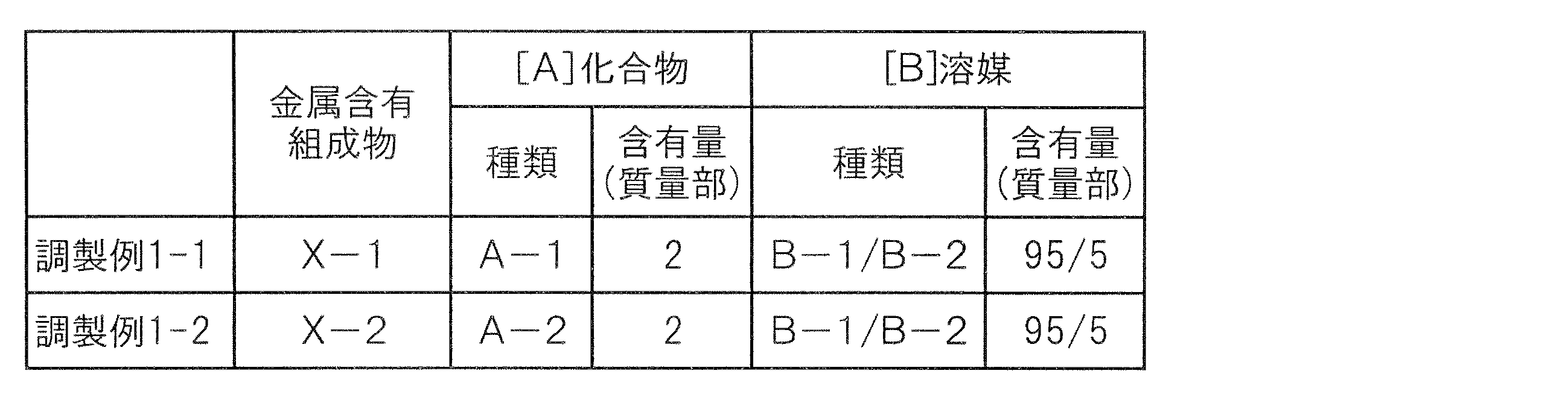
- Preparation Example 1-2 A metal-containing composition (X-2) was prepared in the same manner as in Preparation Example 1-1 except that the types and contents of the respective components were as shown in Table 1 below.
- Substrate (JF-3) A titanium oxide film having an average thickness of 5 nm was formed on a silicon substrate by a chemical vapor deposition method to obtain a substrate (JF-3).
- the resist composition was prepared as follows.
- sensitivity At the time of the formation of the resist pattern, an exposure dose at which a hole pattern having a diameter of 100 nm is formed was taken as an optimal exposure dose.
- the sensitivity is the same as in Comparative Examples (Example 1-1 and Example 1-2, Comparative Example 1-1, Example 1-3, and Example 1-4, Comparative Example 1) in the case where the same substrate was used. 2.
- Example 1-5 and Example 1-6 when the sensitivity is 5% or more higher than that of Comparative Example 1-3), "A" (good) and the improvement of the sensitivity is less than 5% Was rated as "B" (defect). "-" In the column of sensitivity in Table 2 indicates that it is a standard of evaluation.
- the substrate for evaluation in which the resist pattern was formed was obtained.
- a scanning electron microscope (“S-9380" manufactured by Hitachi High-Technologies Corp.) was used for measuring and observing the resist pattern of the evaluation substrate.
- resist pattern collapse suppression property At the time of the formation of the resist pattern, an exposure dose formed in a one-to-one line and space with a line width of 100 nm was taken as an optimal exposure dose.
- the resist pattern collapse suppressive property is “A” (good) when collapse of the resist pattern formed in the above optimum exposure dose is not confirmed, and “B” (defect) when collapse of the resist pattern is confirmed. It was evaluated.
- TMAH 2.38% by weight aqueous solution of TMAH (20-25 ° C.) Thereafter, the substrate was washed with water and dried to obtain a substrate for evaluation on which a resist pattern was formed.
- resist pattern collapse suppression property A scanning electron microscope ("CG-4000” manufactured by Hitachi High-Technologies Corporation) was used for measuring and observing the resist pattern of the evaluation substrate. An exposure dose at which a one-to-one line and space having a line width of 25 nm was formed on the above-mentioned substrate for evaluation was taken as an optimal exposure dose.
- the resist pattern collapse suppressive property is “A” (good) when collapse of the resist pattern formed in the above optimum exposure dose is not confirmed, and “B” (defect) when collapse of the resist pattern is confirmed. It was evaluated.
- the method for forming a resist pattern and the method for treating a substrate of the present invention it is possible to obtain a resist pattern with high sensitivity and excellent resolution. Therefore, they can be suitably used for extreme ultraviolet or electron beam lithography, and can be suitably used for the manufacture of semiconductor devices etc. for which further miniaturization is expected to progress in the future.
Landscapes
- Physics & Mathematics (AREA)
- General Physics & Mathematics (AREA)
- Engineering & Computer Science (AREA)
- Metallurgy (AREA)
- Chemical & Material Sciences (AREA)
- Organic Chemistry (AREA)
- Plasma & Fusion (AREA)
- Architecture (AREA)
- Structural Engineering (AREA)
- Exposure And Positioning Against Photoresist Photosensitive Materials (AREA)
- Exposure Of Semiconductors, Excluding Electron Or Ion Beam Exposure (AREA)
- Materials For Photolithography (AREA)
Abstract
Description
当該レジストパターン形成方法は、少なくとも一方の表層に金属元素を含有する基板を準備する工程(以下、「準備工程」ともいう)と、上記基板の上記金属元素を含有する表面に対する紫外線の暴露、プラズマの暴露、水の接触、アルカリの接触、酸の接触、過酸化水素の接触及びオゾンの接触のうちの1又は2以上の処理を行う工程(以下、「処理工程」ともいう)と、上記処理工程により処理された表面にレジスト組成物を塗工する工程(以下、「塗工工程」ともいう)と、上記塗工工程により形成されたレジスト膜を極端紫外線又は電子線で露光する工程(以下、「露光工程」ともいう)と、上記露光されたレジスト膜を現像する工程(以下、「現像工程」ともいう)とを備える。さらに、当該レジストパターン形成方法は、上記現像工程により形成されたレジストパターンをマスクとして上記基板をエッチングする工程(以下、「エッチング工程」ともいう)を備えてもよい。
本工程では、少なくとも一方の表層に金属元素を含有する基板(以下、「基板(P)」ともいう)を準備する。「表層」とは、基板の表面から5nmの深さまでの領域を意味する。
第4族の金属元素(a)としては、例えばチタン、ジルコニウム、ハフニウム等が、
第5族の金属元素(a)としては、例えばバナジウム、ニオブ、タンタル等が、
第6族の金属元素(a)としては、例えばクロム、モリブデン、タングステン等が、
第7族の金属元素(a)としては、マンガン、レニウム等が、
第8族の金属元素(a)としては、鉄、ルテニウム、オスミウム等が、
第9族の金属元素(a)としては、コバルト、ロジウム、イリジウム等が、
第10族の金属元素(a)としては、ニッケル、パラジウム、白金等が、
第11族の金属元素(a)としては、銅、銀、金等が、
第12族の金属元素(a)としては、亜鉛、カドミウム、水銀等が、
第13族の金属元素(a)としては、アルミニウム、ガリウム、インジウム等が、
第14族の金属元素(a)としては、ゲルマニウム、スズ、鉛等が、
第15族の金属元素(a)としては、アンチモン、ビスマス等が挙げられる。
金属含有組成物(X)としては、例えば金属-酸素共有結合を有する化合物(以下、「[A]化合物」ともいう)と溶媒(以下、「[B]溶媒」ともいう)とを含有する組成物等が挙げられる。
[b]金属含有化合物は、加水分解性基を有する金属化合物(以下、「金属化合物(I)」ともいう)、金属化合物(I)の加水分解物、金属化合物(I)の加水分解縮合物又はこれらの組み合わせである。金属化合物(I)は、1種単独で又は2種以上組み合わせて使用できる。

チタンを含む化合物として、ジイソプロポキシビス(2,4-ペンタンジオナート)チタン(IV)、テトラn-ブトキシチタン(IV)、テトラn-プロポキシチタン(IV)、トリn-ブトキシモノステアレートチタン(IV)、チタン(IV)ブトキシドオリゴマー、アミノプロピルトリメトキシチタン(IV)、トリエトキシモノ(2,4-ペンタンジオナート)チタン(IV)、トリn-プロポキシモノ(2,4-ペンタンジオナート)チタン(IV)、トリイソプロポキシモノ(2,4-ペンタンジオナート)チタン、ジn-ブトキシビス(2,4-ペンタンジオナート)チタン(IV)等が、
ジルコニウムを含む化合物として、ジブトキシビス(エチルアセトアセテート)ジルコニウム(IV)、ジn-ブトキシビス(2,4-ペンタンジオナート)ジルコニウム(IV)、テトラn-ブトキシジルコニウム(IV)、テトラn-プロポキシジルコニウム(IV)、テトライソプロポキシジルコニウム(IV)、アミノプロピルトリエトキシジルコニウム(IV)、2-(3,4-エポキシシクロヘキシル)エチルトリメトキシジルコニウム(IV)、γ-グリシドキシプロピルトリメトキシジルコニウム(IV)、3-イソシアノプロピルトリメトキシジルコニウム(IV)、トリエトキシモノ(2,4-ペンタンジオナート)ジルコニウム(IV)、トリn-プロポキシモノ(2,4-ペンタンジオナート)ジルコニウム(IV)、トリイソプロポキシモノ(2,4-ペンタンジオナート)ジルコニウム(IV)、トリ(3-メタクリロキシプロピル)メトキシジルコニウム(IV)、トリ(3-アクリロキシプロピル)メトキシジルコニウム(IV)等が、
ハフニウムを含む化合物として、ジイソプロポキシビス(2,4-ペンタンジオナート)ハフニウム(IV)、テトラブトキシハフニウム(IV)、テトライソプロポキシハフニウム(IV)、テトラエトキシハフニウム(IV)、ジクロロビス(シクロペンタジエニル)ハフニウム(IV)等が、
タンタルを含む化合物として、テトラブトキシタンタル(IV)、ペンタブトキシタンタル(V)、ペンタエトキシタンタル(V)等が、
タングステンを含む化合物として、テトラブトキシタングステン(IV)、ペンタブトキシタングステン(V)、ペンタメトキシタングステン(V)、ヘキサブトキシタングステン(VI)、ヘキサエトキシタングステン(VI)、ジクロロビス(シクロペンタジエニル)タングステン(IV)等が、
鉄を含む化合物として、塩化鉄(III)等が、
ルテニウムを含む化合物として、ジアセタト[(S)-(-)-2,2’-ビス(ジフェニルホスフィノ)-1,1’-ビナフチル]ルテニウム(II)等が、
コバルトを含む化合物として、ジクロロ[エチレンビス(ジフェニルホスフィン)]コバルト(II)等が、
亜鉛を含む化合物として、ジイソプロポキシ亜鉛(II)、酢酸亜鉛(II)等が、
インジウムを含む化合物として、酢酸インジウム(III)、トリイソプロポキシインジウム(III)等が、
スズを含む化合物として、テトラエチルジアセトキシスタノキサン、テトラブトキシスズ(IV)、テトライソプロポキシスズ(IV)、t-ブチルトリス(ジエチルアミド)スズ(IV)等が、
ゲルマニウムを含む化合物として、テトライソプロポキシゲルマニウム(IV)等が挙げられる。
金属含有組成物(X)の調製方法としては特に限定されず、例えば[A]化合物、[B]溶媒及び必要に応じて他の成分を所定の割合で混合し、好ましくは、得られた混合溶液を孔径0.2μm以下のフィルターでろ過することにより調製することができる。
本工程では、上記基板(P)の金属元素(a)を含有する表面に対する紫外線の暴露、プラズマの暴露、水の接触、アルカリの接触、酸の接触、過酸化水素の接触及びオゾンの接触のうちの1又は2以上を行う。
紫外線は、10nm以上400nm以下の波長を有する電磁波である。
プラズマは、ガスをプラズマ化したものである。このガスとしては、例えばCHF3、CF4、C2F6、C3F8、SF6等のフッ素系ガス、Cl2、BCl3等の塩素系ガス、O2、O3、H2O等の酸素系ガス、H2、NH3、CO、CO2、CH4、C2H2、C2H4、C2H6、C3H4、C3H6、C3H8、HF、HI、HBr、HCl、NO、NH3、BCl3等の還元性ガスなどが用いられる。これらのガスは混合して用いることもできる。
水としては、純水が好ましいが、本発明の効果を損なわない範囲であれば、少量の水溶性有機溶媒、界面活性剤等を含んでいてもよい。
アルカリの接触は、通常、アルカリを含有する溶液(以下、「アルカリ溶液」ともいう)を用いて行う。アルカリとしては、例えばアンモニア、メチルアミン、ジメチルアミン、トリメチルアミン、エチルアミン、ジエチルアミン、トリエチルアミン、テトラアルキルアンモニウム化合物等の有機アミン、水酸化ナトリウム、水酸化カリウム、炭酸ナトリウム、珪酸ナトリウム、メタ珪酸ナトリウム等の無機アルカリ化合物などが挙げられる。テトラアルキルアンモニウム化合物としては、例えばテトラメチルアンモニウムヒドロキシド(TMAH)、テトラエチルアンモニウムヒドロキシド等のテトラアルキルアンモニウムヒドロキシドなどが挙げられる。アルカリ溶液としては、例えばこれらのアルカリが水に溶解したアルカリ水溶液等が挙げられる。このアルカリ水溶液は、本発明の効果を損なわない範囲であれば、少量の水溶性有機溶媒、界面活性剤等を含んでいてもよい。上記アルカリ水溶液としては、フッ化水素及びその塩並びにフッ素化合物の塩をいずれも含まないことが好ましい。
酸の接触は、通常、酸を含有する溶液(以下、「酸溶液」ともいう)を用いて行う。酸としては、例えば硫酸、塩酸、フッ酸等の無機酸、p-トルエンスルホン酸等の有機酸などが挙げられる。酸溶液としては、例えばこれらの酸が溶解した酸水溶液等が挙げられる。これらの酸水溶液は、本発明の効果を損なわない範囲であれば、少量の水溶性有機溶媒、界面活性剤等を含んでいてもよい。
過酸化水素の接触は、通常、過酸化水素水を用いて行う。過酸化水素水は、本発明の効果を損なわない範囲であれば、少量の水溶性有機溶媒、界面活性剤等を含んでいてもよい。
オゾン(O3)の接触は、通常、オゾンを含有するガスを用いて行う。また、酸素を含む雰囲気で200nm以下の波長の紫外線を照射することにより、オゾンが生成し、オゾンの接触を行うことができる。
本工程では、上記基板(P)の処理工程により処理された表面にレジスト組成物を塗工する。
レジスト組成物としては、例えば酸解離性基を有する重合体及び感放射線性酸発生剤を含有する感放射線性樹脂組成物(化学増幅型レジスト組成物)、アルカリ可溶性樹脂とキノンジアジド系感光剤とからなるポジ型レジスト組成物、アルカリ可溶性樹脂と架橋剤を含有するネガ型レジスト組成物、金属含有化合物を含有する感放射線性組成物(金属レジスト組成物)等が挙げられる。これらの中で、感放射線性樹脂組成物が好ましい。感放射線性樹脂組成物を用いた場合、アルカリ現像液で現像することでポジ型パターンを形成することができ、有機溶媒現像液で現像することでネガ型パターンを形成することができる。レジストパターンの形成には、微細パターンを形成する手法であるダブルパターニング法、ダブルエクスポージャー法等を適宜用いてもよい。
本工程では、上記塗工工程により形成されたレジスト膜を極端紫外線又は電子線で露光する。この露光は、例えばマスクにより選択的に放射線を照射して行う。
本工程では、上記露光されたレジスト膜を現像する。これにより、レジストパターンが形成される。
本工程では、上記現像工程により形成されたレジストパターンをマスクとして上記基板をエッチングする。より具体的には、上記レジストパターンをマスクとした1又は複数回のエッチングを行って、パターニングされた基板を得る。
基板(P)において、上記基材と金属含有層(T)との間に、有機下層膜を設けてもよい。有機下層膜は、金属含有層(T)とは異なるものである。有機下層膜は、レジストパターン形成において、金属含有層(T)及び/又はレジスト膜が有する機能をさらに補ったり、これらが有していない機能を得るために、必要とされる所定の機能(例えば反射防止性、塗布膜平坦性、フッ素系ガスに対する高エッチング耐性)を付与したりする膜のことである。
当該基板の処理方法は、極端紫外線又は電子線の露光によりレジストパターンを形成するために用いられ、少なくとも一方の表層に金属元素を含有する基板を処理する方法であって、上記基板の上記金属元素を含有する表面に対する紫外線の暴露、プラズマの暴露、水の接触、アルカリの接触、酸の接触、過酸化水素の接触及びオゾンの接触のうちの1又は2以上の処理を行う工程を備えることを特徴とする。
[A]化合物の溶液0.5gを250℃で30分間焼成することで、この溶液0.5g中の固形分の質量を測定し、この固形分の質量を[A]化合物の溶液の質量で除することにより、[A]化合物の溶液の固形分濃度(質量%)を算出した。
GPCカラム(東ソー(株)の「AWM-H」2本、「AW-H」1本及び「AW2500」2本)を使用し、流量:0.3mL/分、溶出溶媒:N,N’-ジメチルアセトアミドにLiBr(30mM)及びクエン酸(30mM)を添加したもの、カラム温度:40℃の分析条件で、単分散ポリスチレンを標準とするゲルパーミエーションクロマトグラフィー(検出器:示差屈折計)により測定した。
膜の平均厚みは、分光エリプソメータ(J.A.WOOLLAM社の「M2000D」)を用いて測定した。
[[A]化合物の合成]
[A]化合物の合成に用いた金属含有化合物を以下に示す。なお、以下の合成例においては特に断りのない限り、「質量部」は使用した金属含有化合物の合計質量を100質量部とした場合の値を意味する。
M-1:ジイソプロポキシビス(2,4-ペンタンジオナート)チタン(IV)(75質量%濃度の2-プロパノール溶液)
M-2:ジブトキシビス(エチルアセトアセテート)ジルコニウム(IV)(70質量%濃度のn-ブタノール溶液)
反応容器内において、化合物(M-1)(100質量部。但し溶媒を除く。)をプロピレングリコールモノエチルエーテル468質量部に溶解させた。上記反応容器内において、室温(25℃~30℃)で撹拌しながら、水53質量部を10分かけて滴下した。次いで、60℃で反応を2時間実施した。反応終了後、反応容器内を30℃以下に冷却した。冷却した反応溶液に、プロピレングリコールモノエチルエーテル654質量部を加えた後、エバポレーターを用いて、水、反応により生成したアルコール及び余剰のプロピレングリコールモノエチルエーテルを除去して、化合物(A-1)のプロピレングリコールモノエチルエーテル溶液を得た。化合物(A-1)のMwは4,200であった。この化合物(A-1)のプロピレングリコールモノエチルエーテル溶液の固形分濃度は、7.6質量%であった。
反応容器内において、化合物(M-2)(100質量部。但し溶媒を除く。)をプロピレングリコールモノエチルエーテル1,325質量部に溶解させた。上記反応容器内において、室温(25℃~30℃)で撹拌しながら水7質量部を10分かけて滴下した。次いで、60℃で反応を2時間実施した。反応終了後、反応容器内を30℃以下に冷却した。冷却した反応溶液に、プロピレングリコールモノエチルエーテル981質量部を加えた後、エバポレーターを用いて、水、反応により生成したアルコール及び余剰のプロピレングリコールモノエチルエーテルを除去して、化合物(A-2)のプロピレングリコールモノエチルエーテル溶液を得た。化合物(A-2)のMwは2,400であった。この化合物(A-2)のプロピレングリコールモノエチルエーテル溶液の固形分濃度は、13.0質量%であった。
金属含有組成物の調製に用いた[B]溶媒について以下に示す。
B-1:プロピレングリコールモノエチルエーテル
B-2:酢酸プロピレングリコールモノメチルエーテル
[A]化合物(固形分)としての(A-1)2質量部と、[B]溶媒としての(B-1)95質量部([A]化合物の溶液に含まれる溶媒(B-1)も含む)及び(B-2)5質量部とを混合し、得られた溶液を孔径0.2μmのフィルターでろ過して、金属含有組成物(X-1)を調製した。
各成分の種類及び含有量を下記表1に示す通りとした以外は、調製例1-1と同様に操作して、金属含有組成物(X-2)を調製した。
[基板(JF-1)の作製]
シリコン基材上に、上記調製した金属含有組成物(X-1)をスピンコーター(東京エレクトロン(株)の「CLEAN TRACK ACT8」)による回転塗工法により塗工し、220℃で60秒間加熱した後、23℃で30秒間冷却することにより、平均厚み30nmの金属含有層を形成し、基板(JF-1)を得た。
シリコン基材上に、上記調製した金属含有組成物(X-2)を上記スピンコーターによる回転塗工法により塗工し、220℃で60秒間加熱した後、23℃で30秒間冷却することにより、平均厚み30nmの金属含有膜を形成し、基板(JF-2)を得た。
シリコン基材上に、化学気相蒸着法により、平均厚み5nmの酸化チタン膜を形成し、基板(JF-3)を得た。
レジスト組成物を以下のようにして調製した。
レジスト組成物(R-1)は、4-ヒドロキシスチレンに由来する構造単位(1)、スチレンに由来する構造単位(2)及び4-t-ブトキシスチレンに由来する構造単位(3)(各構造単位の含有割合は、(1)/(2)/(3)=65/5/30(モル%))を有する重合体100質量部と、感放射線性酸発生剤としてのトリフェニルスルホニウムサリチレート2.5質量部と、溶媒としての乳酸エチル4,400質量部及び酢酸プロピレングリコールモノメチルエーテル1,900質量部とを混合し、得られた溶液を孔径0.2μmのフィルターでろ過することで得た。
上記作製した基板(JF-1)~(JF-3)のそれぞれについて、下記(P-1)又は(P-2)で示す処理を行った。
P-1:パドル法により、水(20℃~25℃)を基板の表面に接触させた後、スピンコーターによる回転により、乾燥させた。
P-2:基板の表面を、清浄空気中で、10分間、紫外線に暴露した。紫外線光源は、Xeエキシマランプ(ウシオ電機(株)、波長172nm、10mW/cm2)を用いた。
(アルカリ現像液による現像)
[実施例1-1~1-6及び比較例1-1~1-3]
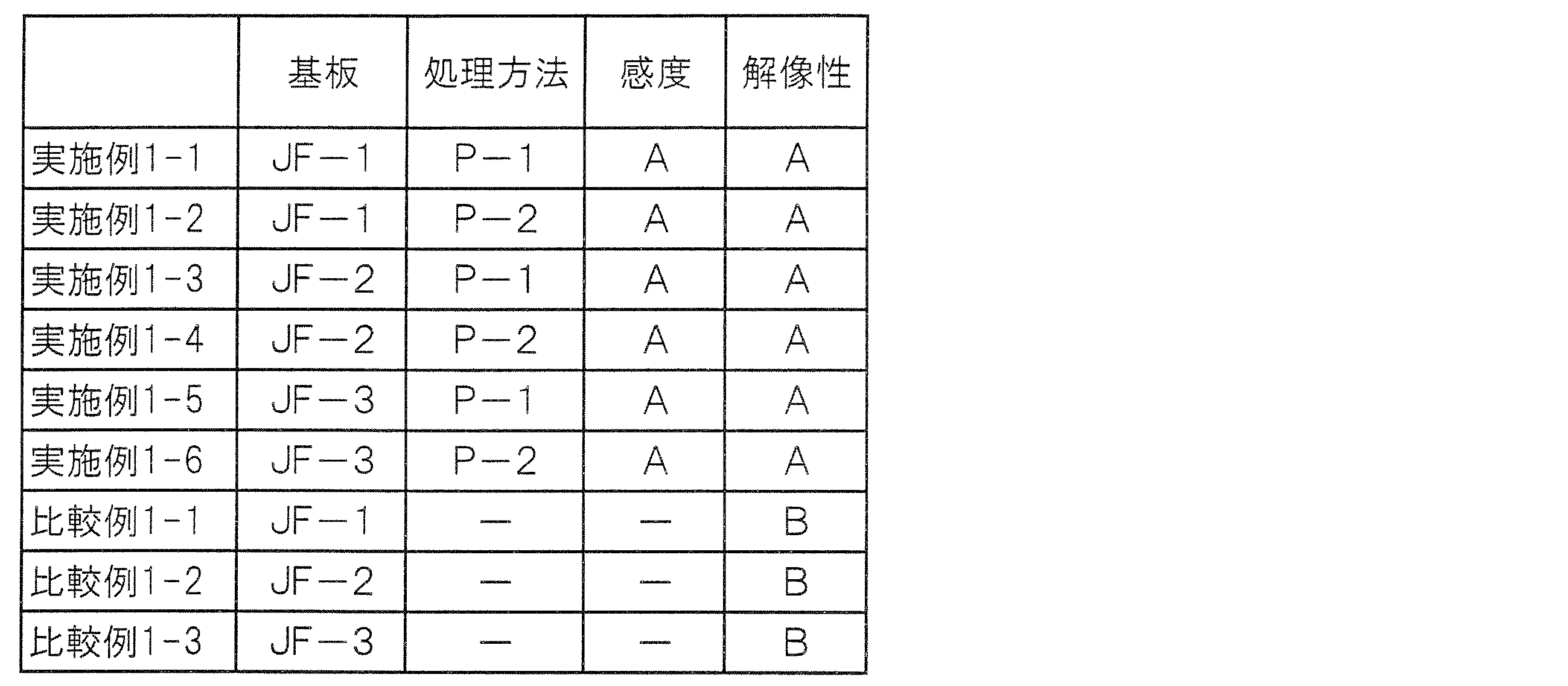
下記表2に示す処理方法で表面を処理した各基板の表面に、レジスト組成物(R-1)を塗工し、130℃で60秒間加熱した後、23℃で30秒間冷却することにより平均厚み50nmのレジスト膜を形成した。次いで、電子線描画装置((株)日立製作所の「HL800D」、出力:50KeV、電流密度:5.0アンペア/cm2)を用いてレジスト膜に電子線を照射した。電子線の照射後、基板を110℃で60秒間加熱を行い、次いで23℃で60秒間冷却した後、2.38質量%のTMAH水溶液(20~25℃)を用い、パドル法により現像した後、水で洗浄し、乾燥することにより、レジストパターンが形成された評価用基板を得た。上記評価用基板のレジストパターンの測長及び観察には走査型電子顕微鏡((株)日立ハイテクノロジーズの「S-9380」)を用いた。
感度及び解像性について、下記方法に従い評価した。評価結果を下記表2に示す。表2の処理方法の欄の「-」は、基板の処理を行わなかったことを示す。
上記レジストパターン形成の際、直径が100nmのホールパターンが形成される露光量を最適露光量とした。感度は、同じ基板を用いた場合についての比較例(実施例1-1及び実施例1-2については比較例1-1、実施例1-3及び実施例1-4については比較例1-2、実施例1-5及び実施例1-6については比較例1-3)に対して5%以上高感度である場合は「A」(良好)と、感度の向上が5%未満の場合は「B」(不良)と評価した。表2の感度の欄の「-」は評価の基準であることを示す。
上記レジストパターン評価の際、直径が80nmのホールパターンが形成される露光量を最適露光量とした。上記評価用基板のレジストパターンの測長及び観察には走査型電子顕微鏡((株)日立ハイテクノロジーズの「S-9380」)を用いた。解像性は、上記最適露光量で形成されたホールパターンにおいて、レジスト膜の残渣が確認されなかった場合は「A」(良好)と、レジスト膜の残渣が確認された場合は「B」(不良)と評価した。
(有機溶媒現像液による現像)
[実施例2-1~2-6及び比較例2-1~2-3]
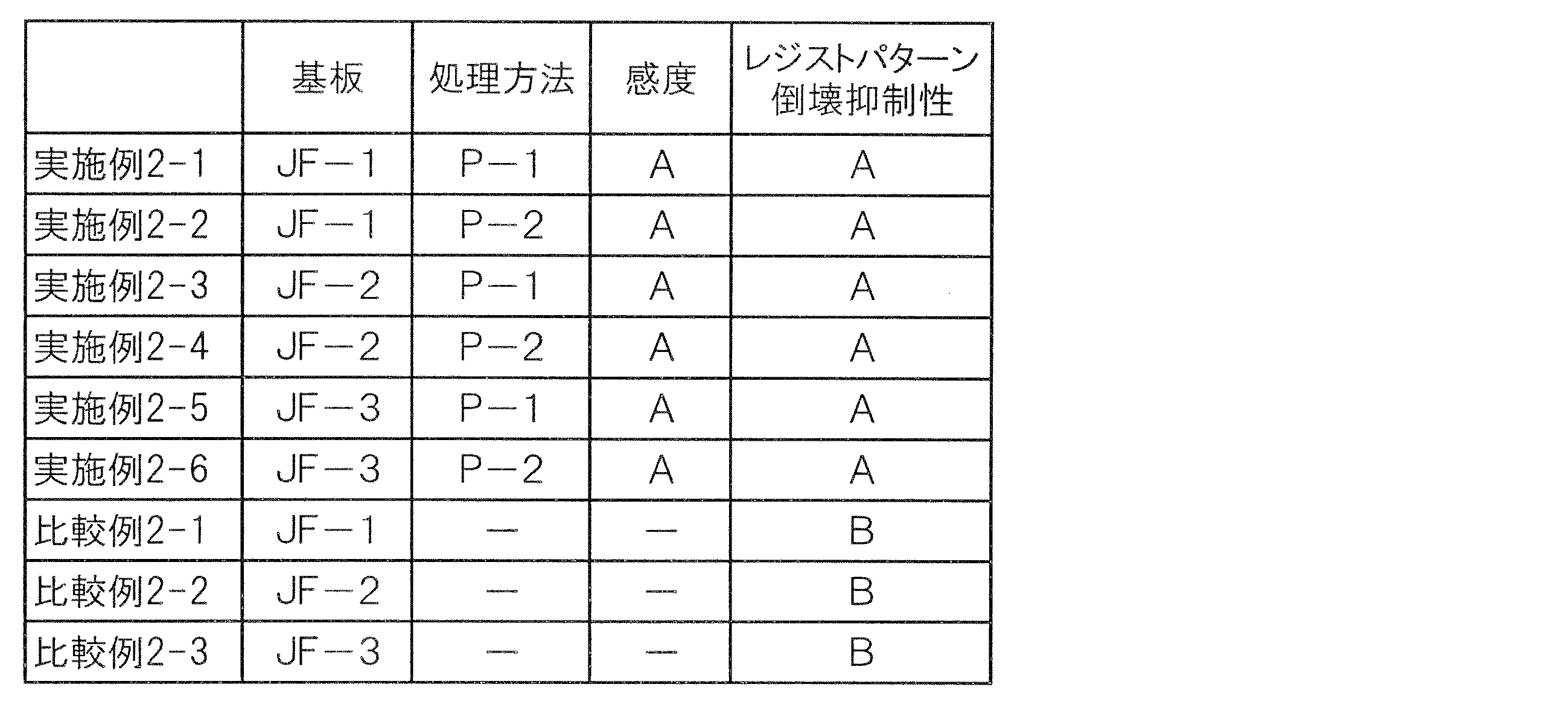
下記表3に示す処理方法で表面を処理した各基板の表面に、レジスト組成物(R-1)を塗工し、130℃で60秒間加熱した後、23℃で30秒間冷却することにより平均厚み50nmのレジスト膜を形成した。次いで、電子線描画装置((株)日立製作所の「HL800D」、出力:50KeV、電流密度:5.0アンペア/cm2)を用いてレジスト膜に電子線を照射した。電子線の照射後、基板を110℃で60秒間加熱を行い、次いで23℃で60秒間冷却した後、酢酸ブチル(20℃~25℃)を用い、パドル法により現像した後、乾燥することにより、レジストパターンが形成された評価用基板を得た。上記評価用基板のレジストパターンの測長及び観察には走査型電子顕微鏡((株)日立ハイテクノロジーズの「S-9380」)を用いた。
感度及びレジストパターン倒壊抑制性について、下記方法に従い評価した。評価結果を下記表3に示す。表3の処理方法の欄の「-」は、基板の処理を行わなかったことを示す。
上記レジストパターン評価の際、線幅150nmの1対1ラインアンドスペースに形成される露光量を最適露光量とした。感度は、同じ基板を用いた場合についての比較例(実施例2-1及び実施例2-2については比較例2-1、実施例2-3及び実施例2-4については比較例2-2、実施例2-5及び実施例2-6については比較例2-3)に対して5%以上高感度である場合は「A」(良好)と、感度の向上が5%未満の場合は「B」(不良)と評価した。表3の感度の欄の「-」は評価の基準であることを示す。
上記レジストパターン形成の際、線幅100nmの1対1ラインアンドスペースに形成される露光量を最適露光量とした。レジストパターン倒壊抑制性は、上記最適露光量において形成されたレジストパターンの倒壊が確認されなかった場合は「A」(良好)と、レジストパターンの倒壊が確認された場合は「B」(不良)と評価した。
(アルカリ現像液による現像)
[実施例3-1~3-6及び比較例3-1~3-3]
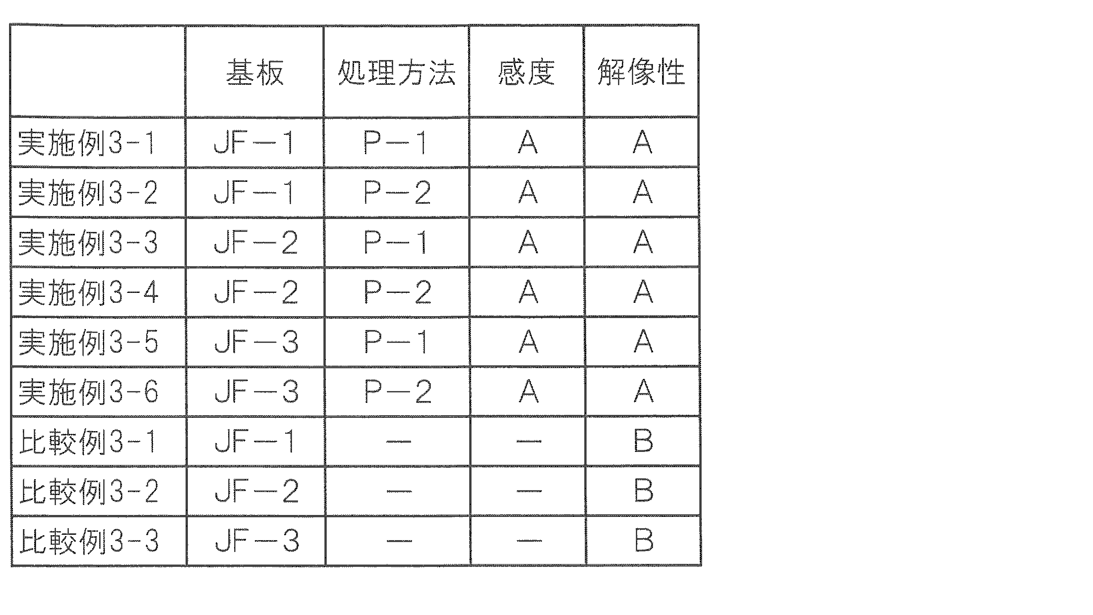
下記表4に示す処理方法で表面を処理した各基板の表面に、レジスト組成物(R-1)を塗工し、130℃で60秒間加熱した後、23℃で30秒間冷却することにより平均厚み50nmのレジスト膜を形成した。次いで、EUVスキャナー(ASML社の「TWINSCAN NXE:3300B」(NA0.3、シグマ0.9、クアドルポール照明、ウェハ上寸法が直径40nmのホールパターンのマスク)を用いてレジスト膜に極端紫外線露光を行った。露光後、基板を110℃で60秒間加熱を行い、次いで23℃で60秒間冷却した。その後、2.38質量%のTMAH水溶液(20~25℃)を用い、パドル法により現像した後、水で洗浄し、乾燥することにより、レジストパターンが形成された評価用基板を得た。
感度及び解像性について、下記方法に従い評価した。評価結果を下記表4に示す。表4の処理方法の欄の「-」は、基板の処理を行わなかったことを示す。
上記評価用基板のレジストパターンの測長及び観察には走査型電子顕微鏡((株)日立ハイテクノロジーズの「CG-4000」)を用いた。上記評価用基板において、直径40nmのホールパターンが形成される露光量を最適露光量とした。感度は、同じ基板を用いた場合についての比較例(実施例3-1及び実施例3-2については比較例3-1、実施例3-3及び実施例3-4については比較例3-2、実施例3-5及び実施例3-6については比較例3-3)に対して5%以上高感度である場合は「A」(良好)と、感度の向上が5%未満の場合は「B」(不良)と評価した。表4の感度の欄の「-」は評価の基準であることを示す。
上記評価用基板のレジストパターンの測長及び観察には走査型電子顕微鏡((株)日立ハイテクノロジーズの「CG-4000」)を用いた。上記評価用基板において、直径40nmのホールパターンが形成される露光量を最適露光量とした。解像性は、上記最適露光量で形成されたホールパターンにおいて、レジスト膜の残渣が確認されなかった場合は「A」(良好)と、レジスト膜の残渣が確認された場合は「B」(不良)と評価した。
(有機溶媒現像液による現像)
[実施例4-1~4-6及び比較例4-1~4-3]
下記表5に示す処理方法で表面を処理した各基板の表面に、レジスト組成物(R-1)を塗工し、130℃で60秒間加熱した後、23℃で30秒間冷却することにより平均厚み50nmのレジスト膜を形成した。次いで、EUVスキャナー(ASML社の「TWINSCAN NXE:3300B」(NA0.3、シグマ0.9、クアドルポール照明、ウェハ上寸法が線幅25nmの1対1ラインアンドスペースのマスク)を用いてレジスト膜に極端紫外線露光を行った。露光後、基板を110℃で60秒間加熱を行い、次いで23℃で60秒間冷却した。その後、酢酸ブチル(20℃~25℃)を用い、パドル法により現像した後、乾燥することにより、レジストパターンが形成された評価用基板を得た。
感度及びレジストパターン倒壊抑制性について、下記方法に従い評価した。評価結果を下記表5に示す。表5の処理方法の欄の「-」は、基板の処理を行わなかったことを示す。
上記評価用基板のレジストパターンの測長及び観察には走査型電子顕微鏡((株)日立ハイテクノロジーズの「CG-4000」)を用いた。上記評価用基板において、線幅25nmの1対1ラインアンドスペースが形成される露光量を最適露光量とした。感度は、同じ基板を用いた場合についての比較例(実施例4-1及び実施例4-2については比較例4-1、実施例4-3及び実施例4-4については比較例4-2、実施例4-5及び実施例4-6については比較例4-3)に対して5%以上高感度である場合は「A」(良好)と、感度の向上が5%未満の場合は「B」(不良)と評価した。表5の感度の欄の「-」は評価の基準であることを示す。
上記評価用基板のレジストパターンの測長及び観察には走査型電子顕微鏡((株)日立ハイテクノロジーズの「CG-4000」)を用いた。上記評価用基板において、線幅25nmの1対1ラインアンドスペースが形成される露光量を最適露光量とした。レジストパターン倒壊抑制性は、上記最適露光量において形成されたレジストパターンの倒壊が確認されなかった場合は「A」(良好)と、レジストパターンの倒壊が確認された場合は「B」(不良)と評価した。

Claims (5)
- 少なくとも一方の表層に金属元素を含有する基板の上記金属元素を含有する表面に対する紫外線の暴露、プラズマの暴露、水の接触、アルカリの接触、酸の接触、過酸化水素の接触及びオゾンの接触のうちの1又は2以上の処理を行う工程と、
上記処理工程により処理された表面にレジスト組成物を塗工する工程と、
上記塗工工程により形成されたレジスト膜を極端紫外線又は電子線で露光する工程と、
上記露光されたレジスト膜を現像する工程と
を備えるレジストパターン形成方法。 - 上記基板の表層の金属元素が周期表第3族~第15族の第3周期~第7周期に属する請求項1に記載のレジストパターン形成方法。
- 上記金属元素が周期表第4族に属する請求項2に記載のレジストパターン形成方法。
- 上記金属元素がチタン、ジルコニウム又はこれらの組み合わせである請求項3に記載のレジストパターン形成方法。
- 極端紫外線又は電子線の露光によりレジストパターンを形成するために用いられ、少なくとも一方の表層に金属元素を含有する基板を処理する方法であって、
上記基板の上記金属元素を含有する表面に対する紫外線の暴露、プラズマの暴露、水の接触、アルカリの接触、酸の接触、過酸化水素の接触及びオゾンの接触のうちの1又は2以上の処理を行う工程
を備えることを特徴とする基板の処理方法。
Priority Applications (3)
| Application Number | Priority Date | Filing Date | Title |
|---|---|---|---|
| JP2019543589A JPWO2019059074A1 (ja) | 2017-09-19 | 2018-09-12 | レジストパターン形成方法及び基板の処理方法 |
| KR1020207007317A KR20200053495A (ko) | 2017-09-19 | 2018-09-12 | 레지스트 패턴 형성 방법 및 기판의 처리 방법 |
| US16/819,315 US20200218161A1 (en) | 2017-09-19 | 2020-03-16 | Resist pattern-forming method and substrate-treating method |
Applications Claiming Priority (2)
| Application Number | Priority Date | Filing Date | Title |
|---|---|---|---|
| JP2017-179588 | 2017-09-19 | ||
| JP2017179588 | 2017-09-19 |
Related Child Applications (1)
| Application Number | Title | Priority Date | Filing Date |
|---|---|---|---|
| US16/819,315 Continuation US20200218161A1 (en) | 2017-09-19 | 2020-03-16 | Resist pattern-forming method and substrate-treating method |
Publications (1)
| Publication Number | Publication Date |
|---|---|
| WO2019059074A1 true WO2019059074A1 (ja) | 2019-03-28 |
Family
ID=65809838
Family Applications (1)
| Application Number | Title | Priority Date | Filing Date |
|---|---|---|---|
| PCT/JP2018/033892 Ceased WO2019059074A1 (ja) | 2017-09-19 | 2018-09-12 | レジストパターン形成方法及び基板の処理方法 |
Country Status (5)
| Country | Link |
|---|---|
| US (1) | US20200218161A1 (ja) |
| JP (1) | JPWO2019059074A1 (ja) |
| KR (1) | KR20200053495A (ja) |
| TW (1) | TWI769312B (ja) |
| WO (1) | WO2019059074A1 (ja) |
Cited By (5)
| Publication number | Priority date | Publication date | Assignee | Title |
|---|---|---|---|---|
| JP2023530299A (ja) * | 2020-06-22 | 2023-07-14 | ラム リサーチ コーポレーション | 金属含有フォトレジスト堆積のための表面改質 |
| JP2023535349A (ja) * | 2020-07-17 | 2023-08-17 | ラム リサーチ コーポレーション | 感光性ハイブリッド膜の形成方法 |
| US12436464B2 (en) | 2020-04-03 | 2025-10-07 | Lam Research Corporation | Pre-exposure photoresist curing to enhance EUV lithographic performance |
| US12585184B2 (en) | 2019-06-28 | 2026-03-24 | Lam Research Corporation | Photoresist with multiple patterning radiation-absorbing elements and/or vertical composition gradient |
| US12601974B2 (en) | 2019-06-28 | 2026-04-14 | Lam Research Corporation | Bake strategies to enhance lithographic performance of metal-containing resist |
Families Citing this family (3)
| Publication number | Priority date | Publication date | Assignee | Title |
|---|---|---|---|---|
| JP7149241B2 (ja) * | 2019-08-26 | 2022-10-06 | 信越化学工業株式会社 | レジスト材料及びパターン形成方法 |
| JP7264771B2 (ja) | 2019-08-30 | 2023-04-25 | 信越化学工業株式会社 | レジスト材料及びパターン形成方法 |
| KR102880818B1 (ko) | 2020-05-04 | 2025-11-05 | 주식회사 엘지에너지솔루션 | 소화부가 구비된 전지 모듈 |
Citations (2)
| Publication number | Priority date | Publication date | Assignee | Title |
|---|---|---|---|---|
| JPH04338959A (ja) * | 1991-05-01 | 1992-11-26 | Dainippon Printing Co Ltd | パターンの形成方法 |
| WO2016181753A1 (ja) * | 2015-05-13 | 2016-11-17 | 富士フイルム株式会社 | プレリンス液、プレリンス処理方法、及び、パターン形成方法 |
Family Cites Families (8)
| Publication number | Priority date | Publication date | Assignee | Title |
|---|---|---|---|---|
| JPS61256723A (ja) * | 1985-05-10 | 1986-11-14 | Fujitsu Ltd | X線マスクの形成方法 |
| JPH04275554A (ja) * | 1991-03-04 | 1992-10-01 | Dainippon Printing Co Ltd | レジストパターン形成方法 |
| JP4369203B2 (ja) | 2003-03-24 | 2009-11-18 | 信越化学工業株式会社 | 反射防止膜材料、反射防止膜を有する基板及びパターン形成方法 |
| JP5862894B2 (ja) | 2010-09-21 | 2016-02-16 | 日産化学工業株式会社 | 保護された脂肪族アルコールを含有する有機基を有するシリコン含有レジスト下層膜形成組成物 |
| US9091934B2 (en) * | 2010-12-24 | 2015-07-28 | Hoya Corporation | Mask blank, method of manufacturing the same, transfer mask, and method of manufacturing the same |
| US8795774B2 (en) * | 2012-09-23 | 2014-08-05 | Rohm And Haas Electronic Materials Llc | Hardmask |
| JP2014164044A (ja) * | 2013-02-22 | 2014-09-08 | Tokyo Ohka Kogyo Co Ltd | 感光性樹脂組成物、パターン形成方法、及び、相分離構造を含む構造体の製造方法 |
| US10866516B2 (en) * | 2016-08-05 | 2020-12-15 | Taiwan Semiconductor Manufacturing Co., Ltd. | Metal-compound-removing solvent and method in lithography |
-
2018
- 2018-09-12 KR KR1020207007317A patent/KR20200053495A/ko not_active Ceased
- 2018-09-12 WO PCT/JP2018/033892 patent/WO2019059074A1/ja not_active Ceased
- 2018-09-12 JP JP2019543589A patent/JPWO2019059074A1/ja active Pending
- 2018-09-17 TW TW107132652A patent/TWI769312B/zh active
-
2020
- 2020-03-16 US US16/819,315 patent/US20200218161A1/en not_active Abandoned
Patent Citations (2)
| Publication number | Priority date | Publication date | Assignee | Title |
|---|---|---|---|---|
| JPH04338959A (ja) * | 1991-05-01 | 1992-11-26 | Dainippon Printing Co Ltd | パターンの形成方法 |
| WO2016181753A1 (ja) * | 2015-05-13 | 2016-11-17 | 富士フイルム株式会社 | プレリンス液、プレリンス処理方法、及び、パターン形成方法 |
Cited By (6)
| Publication number | Priority date | Publication date | Assignee | Title |
|---|---|---|---|---|
| US12585184B2 (en) | 2019-06-28 | 2026-03-24 | Lam Research Corporation | Photoresist with multiple patterning radiation-absorbing elements and/or vertical composition gradient |
| US12601974B2 (en) | 2019-06-28 | 2026-04-14 | Lam Research Corporation | Bake strategies to enhance lithographic performance of metal-containing resist |
| US12436464B2 (en) | 2020-04-03 | 2025-10-07 | Lam Research Corporation | Pre-exposure photoresist curing to enhance EUV lithographic performance |
| JP2023530299A (ja) * | 2020-06-22 | 2023-07-14 | ラム リサーチ コーポレーション | 金属含有フォトレジスト堆積のための表面改質 |
| US12586765B2 (en) | 2020-06-22 | 2026-03-24 | Lam Research Corporation | Surface modification for metal-containing photoresist deposition |
| JP2023535349A (ja) * | 2020-07-17 | 2023-08-17 | ラム リサーチ コーポレーション | 感光性ハイブリッド膜の形成方法 |
Also Published As
| Publication number | Publication date |
|---|---|
| KR20200053495A (ko) | 2020-05-18 |
| US20200218161A1 (en) | 2020-07-09 |
| TW201921154A (zh) | 2019-06-01 |
| JPWO2019059074A1 (ja) | 2020-11-05 |
| TWI769312B (zh) | 2022-07-01 |
Similar Documents
| Publication | Publication Date | Title |
|---|---|---|
| WO2019059074A1 (ja) | レジストパターン形成方法及び基板の処理方法 | |
| KR102611177B1 (ko) | 극단 자외선 또는 전자선 리소그래피용 금속 함유막 형성 조성물, 극단 자외선 또는 전자선 리소그래피용 금속 함유막 및 패턴 형성 방법 | |
| JP7168715B2 (ja) | 半導体フォトレジスト用組成物およびこれを利用したパターン形成方法 | |
| KR102351281B1 (ko) | 다층 레지스트 프로세스용 무기 막 형성 조성물 및 패턴 형성 방법 | |
| KR20180121550A (ko) | 감방사선성 조성물 및 패턴 형성 방법 | |
| JP6399083B2 (ja) | 多層レジストプロセス用組成物および該多層レジストプロセス用組成物を用いたパターン形成方法 | |
| JPWO2019220835A1 (ja) | パターン形成方法及び感放射線性組成物 | |
| KR102848490B1 (ko) | 조성물, 막, 막 형성 방법, 패턴 형성 방법, 유기 하층막 반전 패턴 형성 방법 및 조성물의 제조 방법 | |
| KR102646535B1 (ko) | 패터닝된 기판의 제조 방법 | |
| TW201739842A (zh) | 表面處理用組成物及使用其之光阻圖案之表面處理方法 | |
| KR102518770B1 (ko) | 클러스터 화합물 또는 이의 염 및 이를 포함하는 포토레지스트 조성물 | |
| TW202013098A (zh) | 半導體基板的處理方法 | |
| EP4647840A2 (en) | Compound for forming metal-containing film, compositon for forming metal-containing film, and patterning process | |
| EP4653955A2 (en) | Compound for forming metal-containing film, composition for forming metal-containing film, and patterning process | |
| EP4579348A2 (en) | Compound for forming metal-containing film, composition for forming metal-containing film, and patterning process | |
| EP4579346A2 (en) | Compound for forming metal-containing film, composition for forming metal-containing film, and patterning process | |
| TW202611053A (zh) | 半導體製造用組成物及膜形成方法 | |
| WO2025053057A1 (ja) | 半導体製造用基板、半導体製造用基板の製造方法及び半導体基板の製造方法 | |
| WO2025079496A1 (ja) | 半導体基板の製造方法 | |
| TW202120635A (zh) | 抗蝕劑底層膜形成用組成物、圖案形成方法、及電子器件的製造方法 |
Legal Events
| Date | Code | Title | Description |
|---|---|---|---|
| 121 | Ep: the epo has been informed by wipo that ep was designated in this application |
Ref document number: 18858395 Country of ref document: EP Kind code of ref document: A1 |
|
| ENP | Entry into the national phase |
Ref document number: 2019543589 Country of ref document: JP Kind code of ref document: A |
|
| ENP | Entry into the national phase |
Ref document number: 20207007317 Country of ref document: KR Kind code of ref document: A |
|
| NENP | Non-entry into the national phase |
Ref country code: DE |
|
| 122 | Ep: pct application non-entry in european phase |
Ref document number: 18858395 Country of ref document: EP Kind code of ref document: A1 |