WO2019047386A1 - Oled像素驱动电路及oled显示装置 - Google Patents
Oled像素驱动电路及oled显示装置 Download PDFInfo
- Publication number
- WO2019047386A1 WO2019047386A1 PCT/CN2017/113032 CN2017113032W WO2019047386A1 WO 2019047386 A1 WO2019047386 A1 WO 2019047386A1 CN 2017113032 W CN2017113032 W CN 2017113032W WO 2019047386 A1 WO2019047386 A1 WO 2019047386A1
- Authority
- WO
- WIPO (PCT)
- Prior art keywords
- thin film
- film transistor
- pin
- signal
- voltage
- Prior art date
- Legal status (The legal status is an assumption and is not a legal conclusion. Google has not performed a legal analysis and makes no representation as to the accuracy of the status listed.)
- Ceased
Links
Images

Classifications
-
- G—PHYSICS
- G09—EDUCATION; CRYPTOGRAPHY; DISPLAY; ADVERTISING; SEALS
- G09G—ARRANGEMENTS OR CIRCUITS FOR CONTROL OF INDICATING DEVICES USING STATIC MEANS TO PRESENT VARIABLE INFORMATION
- G09G3/00—Control arrangements or circuits, of interest only in connection with visual indicators other than cathode-ray tubes
- G09G3/20—Control arrangements or circuits, of interest only in connection with visual indicators other than cathode-ray tubes for presentation of an assembly of a number of characters, e.g. a page, by composing the assembly by combination of individual elements arranged in a matrix no fixed position being assigned to or needed to be assigned to the individual characters or partial characters
- G09G3/22—Control arrangements or circuits, of interest only in connection with visual indicators other than cathode-ray tubes for presentation of an assembly of a number of characters, e.g. a page, by composing the assembly by combination of individual elements arranged in a matrix no fixed position being assigned to or needed to be assigned to the individual characters or partial characters using controlled light sources
- G09G3/30—Control arrangements or circuits, of interest only in connection with visual indicators other than cathode-ray tubes for presentation of an assembly of a number of characters, e.g. a page, by composing the assembly by combination of individual elements arranged in a matrix no fixed position being assigned to or needed to be assigned to the individual characters or partial characters using controlled light sources using electroluminescent panels
- G09G3/32—Control arrangements or circuits, of interest only in connection with visual indicators other than cathode-ray tubes for presentation of an assembly of a number of characters, e.g. a page, by composing the assembly by combination of individual elements arranged in a matrix no fixed position being assigned to or needed to be assigned to the individual characters or partial characters using controlled light sources using electroluminescent panels semiconductive, e.g. using light-emitting diodes [LED]
- G09G3/3208—Control arrangements or circuits, of interest only in connection with visual indicators other than cathode-ray tubes for presentation of an assembly of a number of characters, e.g. a page, by composing the assembly by combination of individual elements arranged in a matrix no fixed position being assigned to or needed to be assigned to the individual characters or partial characters using controlled light sources using electroluminescent panels semiconductive, e.g. using light-emitting diodes [LED] organic, e.g. using organic light-emitting diodes [OLED]
- G09G3/3225—Control arrangements or circuits, of interest only in connection with visual indicators other than cathode-ray tubes for presentation of an assembly of a number of characters, e.g. a page, by composing the assembly by combination of individual elements arranged in a matrix no fixed position being assigned to or needed to be assigned to the individual characters or partial characters using controlled light sources using electroluminescent panels semiconductive, e.g. using light-emitting diodes [LED] organic, e.g. using organic light-emitting diodes [OLED] using an active matrix
- G09G3/3233—Control arrangements or circuits, of interest only in connection with visual indicators other than cathode-ray tubes for presentation of an assembly of a number of characters, e.g. a page, by composing the assembly by combination of individual elements arranged in a matrix no fixed position being assigned to or needed to be assigned to the individual characters or partial characters using controlled light sources using electroluminescent panels semiconductive, e.g. using light-emitting diodes [LED] organic, e.g. using organic light-emitting diodes [OLED] using an active matrix with pixel circuitry controlling the current through the light-emitting element
Definitions
- the present invention relates to the field of display technologies, and in particular, to an OLED pixel driving circuit and an OLED display device.
- OLED Organic Light Emitting Display
- OLED Organic Light Emitting Display
- the OLED is a current driving device.
- the organic light emitting diode emits light, and the luminance of the light is determined by the current flowing through the organic light emitting diode itself.
- Most existing integrated circuits (ICs) only transmit voltage signals, so the pixel driving circuit of the OLED needs to complete the task of converting the voltage signal into a current signal.
- the conventional OLED pixel driving circuit is usually 2T1C, that is, a structure in which two thin film transistors are added with a capacitor to convert a voltage into a current.
- a conventional 2T1C pixel driving circuit for an OLED includes: a first thin film transistor T10, a second thin film transistor T20, and a capacitor C10, the first thin film transistor T10 is a switching thin film transistor, and the second The thin film transistor T20 is a driving thin film transistor, and the capacitor C10 is a storage capacitor.
- the gate of the first thin film transistor T10 is connected to the scan signal Scan, the drain is connected to the data signal Data, the source is electrically connected to the gate of the second thin film transistor T20, and one end of the capacitor C10; the second The drain of the thin film transistor T20 is connected to the power supply voltage OVDD, the source is electrically connected to the anode of the organic light emitting diode D10, the cathode of the organic light emitting diode D10 is connected to the common ground voltage OVSS, and one end of the capacitor C10 is electrically connected to the second thin film transistor T20.
- the gate is electrically connected to the source of the second thin film transistor T20.
- the scan signal Scan controls the first thin film transistor T10 to be turned on, and the data signal Data passes through the first thin film transistor T10 to enter the gate of the second thin film transistor T20 and the capacitor C10, and then the first thin film transistor T10 is turned off due to the capacitance.
- the storage function of C10, the gate voltage of the second thin film transistor T20 can continue to maintain the data signal voltage, so that the second thin film transistor T20 is in an on state, and the driving current enters the organic light emitting diode D10 through the second thin film transistor T20 to drive the organic light emitting. Diode D10 emits light.
- I OLED K ⁇ (Vgs - Vth) 2 ;
- I OLED represents the current flowing through the driving thin film transistor and the organic light emitting diode
- K is the intrinsic conductive factor of the driving thin film transistor
- Vgs represents the voltage difference between the gate and the source of the driving thin film transistor
- Vth represents the driving thin film transistor Threshold voltage. It can be seen that the size of the I OLED is related to the threshold voltage Vth of the driving thin film transistor.
- the above-mentioned conventional OLED pixel driving circuit has a simple structure and does not have a compensation function, so there are many defects, and among them, the driving thin film transistor of each pixel in the OLED display device is relatively obvious due to non-uniformity in the manufacturing process of the thin film transistor.
- the threshold voltages are inconsistent; and the long-term operation causes the material of the driving thin film transistor to age, which causes the threshold voltage of the driving thin film transistor to drift, which may cause display unevenness.
- some OLED pixel driving circuits are capable of sensing the threshold voltage of the driving thin film transistor and compensating the threshold voltage into the data signal, but the voltage of the data signal is affected by the threshold voltage of the organic light emitting diode.
- the threshold voltage of the organic light-emitting diode is required to be about 10V, and the light-emitting layer in the organic light-emitting diode must adopt a three-layer or four-layer structure; on the other hand, the data signal voltage in the data signal writing stage cannot be greater than The threshold voltage of the organic light-emitting diode is ensured that the organic light-emitting diode is not illuminated during the data signal writing phase; in addition, the gate voltage of the driving thin film transistor is also affected by the threshold voltage of the organic light-emitting diode, requiring In the data signal writing phase, the gate voltage of the driving thin film transistor cannot be greater than the sum of the threshold voltage of the organic light emitting diode and the threshold voltage of the driving thin film
- An object of the present invention is to provide an OLED pixel driving circuit, which not only has a compensation function, but also can eliminate the influence of the threshold voltage of the driving thin film transistor on the current flowing through the organic light emitting diode, improve display uniformity, and can also enable voltage and driving of the data signal.
- the gate voltage of the thin film transistor is not affected by the threshold voltage of the organic light emitting diode.
- Another object of the present invention is to provide an OLED display device, wherein the pixel driving circuit has a compensation function, and the display uniformity is good, and the voltage of the data signal and the gate voltage of the driving thin film transistor are not affected by the threshold of the organic light emitting diode. The effect of voltage.
- the present invention first provides an OLED pixel driving circuit including a first thin film transistor, a second thin film transistor, a third thin film transistor, a fourth thin film transistor, a fifth thin film transistor, a capacitor, an organic light emitting diode, and a setting a switching switch, a digital-to-analog converter, and an analog-to-digital converter in the driving IC; an operating state of the OLED pixel driving circuit includes a display mode and a sensing mode;
- the switch is controlled by a switching signal, including a first pin, a second pin, and a third lead foot;
- the gate of the first thin film transistor is connected to the scan signal, the drain is connected to the power supply voltage, and the source is electrically connected to the drain of the second thin film transistor, the gate of the fourth thin film transistor, and one end of the capacitor;
- the gate of the second thin film transistor is connected to the scan signal, the source is connected to the common ground voltage;
- the drain of the fourth thin film transistor is connected to the power supply voltage, and the source is electrically connected to the drain of the fifth thin film transistor;
- the gate of the fifth thin film transistor is connected to the light emission control signal, the source is electrically connected to the anode of the organic light emitting diode; the cathode of the organic light emitting diode is connected to the common ground voltage; and the other end of the capacitor is electrically connected to the source of the fourth thin film transistor;
- the gate of the three thin film transistor is connected to the scan signal in the display mode, the sensing control signal is connected in the sensing mode, the source is electrically connected to the source of the fourth thin film transistor, and
- the second pin of the switch is electrically connected to the digital-to-analog converter, and the third pin is electrically connected to the analog-to-digital converter;
- the switching signal control switch is turned on to the first pin and the second pin, and the digital-to-analog converter provides a data signal; the display mode is divided into a data signal writing phase and an illumination phase, and the illumination control signal is written.
- the input phase is low, so that the fifth thin film transistor is turned off, and the fifth thin film transistor is turned on during the light emitting phase; in the sensing mode, the digital-to-analog converter first provides a low potential signal, and then switches the signal control switch.
- the first pin and the third pin are turned on, so that the analog to digital converter senses the threshold voltage of the fourth thin film transistor.
- the scan signal In the data writing phase of the display mode: the scan signal is high, the common ground voltage is low, the data signal is high; in the light-emitting phase of the display mode: the scan signal is low, The common ground voltage is low, and the data signal is high;
- the scan signal first provides a high-potential pulse, and then remains low;
- the sensing control signal first provides a high-potential pulse synchronized with the high-potential pulse of the scan signal, and then remains low;
- the common ground voltage is always low;
- the illumination control signal is always low.
- the resistance value of the first thin film transistor is proportional to the resistance value of the second thin film transistor.
- the maximum value of the preset data signal voltage of the driving IC corresponds to the lowest gray level, and the minimum value of the data signal voltage corresponds to the highest gray level; by adjusting the ratio of the resistance value of the first thin film transistor to the resistance value of the second thin film transistor The relationship is such that the gate voltage of the fourth thin film transistor is equal to the sum of the maximum value of the data signal voltage and the threshold voltage of the fourth thin film transistor.
- the present invention also provides an OLED display device including an OLED pixel driving circuit, the OLED pixel driving circuit including a first thin film transistor, a second thin film transistor, a third thin film transistor, a fourth thin film transistor, a fifth thin film transistor, a capacitor, An organic light emitting diode, and a switch, a digital to analog converter, and an analog to digital converter disposed in the driving IC; the OLED pixel
- the operating state of the driving circuit includes a display mode and a sensing mode;
- the switch is controlled by a switching signal, including a first pin, a second pin, and a third pin;
- the gate of the first thin film transistor is connected to the scan signal, the drain is connected to the power supply voltage, and the source is electrically connected to the drain of the second thin film transistor, the gate of the fourth thin film transistor, and one end of the capacitor;
- the gate of the second thin film transistor is connected to the scan signal, the source is connected to the common ground voltage;
- the drain of the fourth thin film transistor is connected to the power supply voltage, and the source is electrically connected to the drain of the fifth thin film transistor;
- the gate of the fifth thin film transistor is connected to the light emission control signal, the source is electrically connected to the anode of the organic light emitting diode; the cathode of the organic light emitting diode is connected to the common ground voltage; and the other end of the capacitor is electrically connected to the source of the fourth thin film transistor;
- the gate of the three thin film transistor is connected to the scan signal in the display mode, the sensing control signal is connected in the sensing mode, the source is electrically connected to the source of the fourth thin film transistor, and
- the second pin of the switch is electrically connected to the digital-to-analog converter, and the third pin is electrically connected to the analog-to-digital converter;
- the switching signal control switch is turned on to the first pin and the second pin, and the digital-to-analog converter provides a data signal; the display mode is divided into a data signal writing phase and an illumination phase, and the illumination control signal is written.
- the input phase is low, so that the fifth thin film transistor is turned off, and the fifth thin film transistor is turned on during the light emitting phase; in the sensing mode, the digital-to-analog converter first provides a low potential signal, and then switches the signal control switch.
- the first pin and the third pin are turned on, so that the analog to digital converter senses the threshold voltage of the fourth thin film transistor.
- the scan signal In the data writing phase of the display mode: the scan signal is high, the common ground voltage is low, the data signal is high; in the light-emitting phase of the display mode: the scan signal is low, The common ground voltage is low, and the data signal is high;
- the scan signal first provides a high-potential pulse, and then remains low;
- the sensing control signal first provides a high-potential pulse synchronized with the high-potential pulse of the scan signal, and then remains low;
- the common ground voltage is always low;
- the illumination control signal is always low.
- the resistance value of the first thin film transistor is proportional to the resistance value of the second thin film transistor.
- the maximum value of the preset data signal voltage of the driving IC corresponds to the lowest gray level, and the minimum value of the data signal voltage corresponds to the highest gray level; by adjusting the ratio of the resistance value of the first thin film transistor to the resistance value of the second thin film transistor The relationship is such that the gate voltage of the fourth thin film transistor is equal to the sum of the maximum value of the data signal voltage and the threshold voltage of the fourth thin film transistor.
- the present invention also provides an OLED pixel driving circuit including a first thin film transistor, a second thin film transistor, a third thin film transistor, a fourth thin film transistor, a fifth thin film transistor, a capacitor, An organic light emitting diode, and a switch, a digital to analog converter, and an analog to digital converter disposed in the driving IC; the operating states of the OLED pixel driving circuit include a display mode and a sensing mode;
- the switch is controlled by a switching signal, including a first pin, a second pin, and a third pin;
- the gate of the first thin film transistor is connected to the scan signal, the drain is connected to the power supply voltage, and the source is electrically connected to the drain of the second thin film transistor, the gate of the fourth thin film transistor, and one end of the capacitor;
- the gate of the second thin film transistor is connected to the scan signal, the source is connected to the common ground voltage;
- the drain of the fourth thin film transistor is connected to the power supply voltage, and the source is electrically connected to the drain of the fifth thin film transistor;
- the gate of the fifth thin film transistor is connected to the light emission control signal, the source is electrically connected to the anode of the organic light emitting diode; the cathode of the organic light emitting diode is connected to the common ground voltage; and the other end of the capacitor is electrically connected to the source of the fourth thin film transistor;
- the gate of the three thin film transistor is connected to the scan signal in the display mode, the sensing control signal is connected in the sensing mode, the source is electrically connected to the source of the fourth thin film transistor, and
- the second pin of the switch is electrically connected to the digital-to-analog converter, and the third pin is electrically connected to the analog-to-digital converter;
- the switching signal control switch is turned on to the first pin and the second pin, and the digital-to-analog converter provides a data signal; the display mode is divided into a data signal writing phase and an illumination phase, and the illumination control signal is written.
- the input phase is low, so that the fifth thin film transistor is turned off, and the fifth thin film transistor is turned on during the light emitting phase; in the sensing mode, the digital-to-analog converter first provides a low potential signal, and then switches the signal control switch. Turning on the first pin and the third pin, so that the analog-to-digital converter senses the threshold voltage of the fourth thin film transistor;
- the scan signal in the data writing phase of the display mode: the scan signal is high, the common ground voltage is low, the data signal is high; in the light-emitting phase of the display mode: the scan signal is low The common ground voltage is a low potential, and the data signal is a high potential;
- the scan signal first provides a high-potential pulse, and then remains low;
- the sensing control signal first provides a high-potential pulse synchronized with the high-potential pulse of the scan signal, and then remains low;
- the common ground voltage is always low;
- the illumination control signal is always low;
- the resistance value of the first thin film transistor is proportional to the resistance value of the second thin film transistor
- the maximum value of the preset data signal voltage of the driving IC corresponds to the lowest gray level, and the minimum value of the data signal voltage corresponds to the highest gray level; by adjusting the resistance value of the first thin film transistor and the resistance value of the second thin film transistor The proportional relationship makes the gate of the fourth thin film transistor The voltage is equal to the sum of the maximum value of the data signal voltage and the threshold voltage of the fourth thin film transistor.
- the invention has the beneficial effects that the OLED pixel driving circuit provided by the invention adopts a 5T1C structure, and is provided with a switching switch, and controls the switching switch to turn on the first pin and the second pin to enter the display mode by switching signals, and controls switching by switching signals.
- the switch turns on the first pin and the third pin to enter the sensing mode, so that the analog-to-digital converter senses the threshold voltage of the fourth thin film transistor, and is used for data compensation in the display mode after analog-to-digital conversion, thereby having compensation
- the function can eliminate the influence of the threshold voltage of the driving thin film transistor on the current flowing through the organic light emitting diode, and improve display uniformity; and control the fifth thin film transistor connected to the organic light emitting diode to be turned off during the data writing phase by the light emission control signal, thereby enabling The voltage of the data signal and the gate voltage of the driving thin film transistor are not affected by the threshold voltage of the organic light emitting diode.
- the OLED display device provided by the invention comprises the OLED pixel driving circuit, has a compensation function, and has good display uniformity, and the voltage of the data signal and the gate voltage of the driving thin film transistor are not affected by the threshold voltage of the organic light emitting diode. influences.
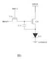
- 1 is a circuit diagram of a conventional 2T1C pixel driving circuit for an OLED
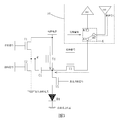
- FIG. 2 is a circuit diagram of an OLED pixel driving circuit of the present invention
- FIG. 3 is a circuit connection diagram of the OLED pixel driving circuit of the present invention in a display mode
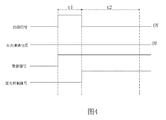
- FIG. 4 is a timing diagram of the OLED pixel driving circuit of the present invention in a display mode
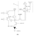
- FIG. 5 is a circuit connection diagram of the OLED pixel driving circuit of the present invention in a sensing mode
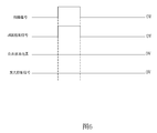
- FIG. 6 is a timing diagram of the OLED pixel driving circuit of the present invention in a sensing mode.
- the present invention provides an OLED pixel driving circuit.
- the OLED pixel driving circuit of the present invention includes a first thin film transistor T1, a second thin film transistor T2, a third thin film transistor T3, a fourth thin film transistor T4, and a fifth thin film transistor T5.
- the body tube T4 is a driving thin film transistor that drives the organic light emitting diode D1.
- the OLED pixel driving circuit adopts a 5T1C structure, and sets a switching switch K, and its working state includes a display mode and a sensing mode.
- the switch K is controlled by the switching signal Switch, and includes a first pin K1, a second pin K2, and a third pin K3;
- the gate of the first thin film transistor T1 is connected to the scan signal Scan, the drain is connected to the power supply voltage OVDD, the source and the drain of the second thin film transistor T2, the gate g of the fourth thin film transistor T4, and the capacitor C1.
- One end of the second thin film transistor T2 is connected to the scan signal Scan, the source is connected to the common ground voltage OVSS; the drain of the fourth thin film transistor T4 is connected to the power supply voltage OVDD, and the source is s
- the fifth thin film transistor T5 is connected to the drain of the fifth thin film transistor T5; the gate of the fifth thin film transistor T5 is connected to the light emission control signal EM, the source is electrically connected to the anode of the organic light emitting diode D1; and the cathode of the organic light emitting diode D1 is connected to the common ground.
- the other end of the capacitor C1 is electrically connected to the source s of the fourth thin film transistor T4; the gate of the third thin film transistor T3 is connected to the scan signal Scan in the display mode, and the sensing control signal is connected in the sensing mode.
- the source is electrically connected to the source s of the fourth thin film transistor T4, the drain is electrically connected to the first pin K1 of the switch K;
- the second pin K2 of the switch K is electrically connected to the digital-to-analog converter DAC, and the third pin K3 is electrically connected to the analog-to-digital converter ADC.
- the first thin film transistor T1, the second thin film transistor T2, the third thin film transistor T3, the fourth thin film transistor T4, and the fifth thin film transistor T5 are all low temperature polysilicon thin film transistors, oxide semiconductor thin film transistors, or amorphous silicon films. Transistor.
- the resistance value of the first thin film transistor T1 has a specific proportional relationship with the resistance value of the second thin film transistor T2.
- the voltage is divided by the power supply voltage OVDD.
- the switching signal Switch controls the switching switch K to turn on the first pin K1 and the second pin K2, and the digital-to-analog converter DAC provides the data signal Data.
- the display mode is further divided into a data signal writing phase t1 and a lighting phase t2.
- the scan signal Scan is at a high potential, so that the first thin film transistor T1, the second thin film transistor T2, and the third thin film transistor T3 are both turned on; the light emission control signal EM is low, so that The fifth thin film transistor T5 is turned off; the common ground voltage OVSS is low; and the data signal Data is high.
- the turned-on first thin film transistor T1 and the second thin film transistor T2 divide the power supply voltage OVDD, so the voltage Vg of the gate g of the fourth thin film transistor T4 is:
- Vg OVDD ⁇ R T2 /(R T2 +R T1 );
- R T1 represents a resistance value of the first thin film transistor T1
- R T2 represents a resistance value of the second thin film transistor T2
- the light emission control signal EM controls the fifth thin film transistor T5 to be turned off, and the connection of the anode of the organic light emitting diode D1 to the source s of the driving thin film transistor, that is, the fourth thin film transistor T4, is cut off, and the organic light emitting diode is cut off.
- D1 does not illuminate, and the threshold voltage of the organic light-emitting diode D1 is required to be a large specific value in order to prevent the organic light-emitting diode D1 from being lit. Therefore, the light-emitting layer in the organic light-emitting diode D1 can be laminated.
- the voltage of the data signal Data cannot be greater than the threshold voltage of the organic light-emitting diode D1, and that the gate voltage Vg of the driving thin film transistor, that is, the fourth thin film transistor T4, cannot be greater than that of the organic light-emitting diode
- the threshold voltage of the stage D1 and the threshold voltage of the driving thin film transistor are the same, so that the voltage of the data signal Data and the gate voltage Vg of the fourth thin film transistor T4 are not affected by the threshold voltage of the organic light emitting diode D1.
- the scan signal Scan is at a low potential, so that the first thin film transistor T1, the second thin film transistor T2, and the third thin film transistor T3 are both turned off; the light emission control signal EM is turned to a high potential, so that The fifth thin film transistor T5 is turned on, the anode of the organic light emitting diode D1 is connected to the source s of the fourth thin film transistor T4; the common ground voltage OVSS is kept at a low potential; the data signal Data is kept at a high potential; and the storage function of the capacitor C1 is relied on The organic light emitting diode D1 emits light for display.
- the maximum value of the internal preset data signal Data voltage of the driving IC 10 corresponds to the lowest gray level, and the minimum value of the data signal Data voltage corresponds to the highest gray level; by adjusting the resistance value of the first thin film transistor T1 and The proportional relationship of the resistance values of the second thin film transistor T2 can change the voltage Vg of the gate g of the fourth thin film transistor T4 to be equal to the sum of the maximum value Vmax Data of the data signal Data voltage and the threshold voltage Vth of the fourth thin film transistor T4, which is:
- This situation can make the dark state display effect of the OLED display device better.
- the scan signal Scan first provides a high potential pulse to turn on the first thin film transistor T1 and the second thin film transistor T2, and the first thin film transistor T1 and the second thin film transistor T2 that are turned on divide the power supply voltage OVDD, and still make
- the voltage Vg of the gate g of the fourth thin film transistor T4 is:
- Vg OVDD ⁇ R T2 /(R T2 +R T1 );
- the illuminating control signal EM is always at a low potential, and the fifth thin film transistor T5 is controlled to be turned off.
- the anode of the organic light emitting diode D1 is disconnected from the source s of the driving thin film transistor, that is, the fourth thin film transistor T4, and the organic light emitting diode D1 is not Will light up;
- the common ground voltage OVSS is always at a low potential
- the sensing control signal Sense first provides a high-potential pulse synchronized with the high-potential pulse of the scan signal Scan to turn on the third thin film transistor T3, and the switching signal Switch first holds the switch K to turn on the first pin K1 and The second pin K2, the digital-to-analog converter DAC first provides a low potential signal to the fourth thin film transistor T4 via the first pin K1 and the second pin K2 of the switch K and the turned-on third thin film transistor T3.
- the source s; next, the switching signal Switch controls the switch K to turn on the first pin K1 and the third pin K3.
- the first pin K1 and the third pin K3 of K enter the analog-to-digital converter ADC such that the analog-to-digital converter ADC senses the threshold voltage Vth of the fourth thin film transistor T4, that is, the driving thin film transistor.
- both the scan signal Scan and the sense control signal Sense are turned to a low potential and held.
- the analog-to-digital converter ADC senses the threshold voltage Vth of the fourth thin film transistor T4, that is, the driving thin film transistor, and converts it into digital sensing data, and stores the digital sensing data for data compensation in the display mode. use. Since the threshold voltage Vth of the fourth thin film transistor T4, that is, the driving thin film transistor, is compensated in the display mode, the current flowing through the organic light emitting diode D1 is independent of the threshold voltage Vth of the driving thin film transistor, and the threshold voltage Vth of the driving thin film transistor is eliminated. The influence of the light-emitting diode D1 can improve the uniformity of display and improve the luminous efficiency.
- the present invention further provides an OLED display device including the above OLED pixel driving circuit, and the structure and function of the OLED pixel driving circuit are not repeatedly described herein.
- the OLED pixel driving circuit of the present invention adopts a 5T1C structure, and is provided with a switching switch.
- the switching signal is controlled by the switching signal to turn on the first pin and the second pin to enter the display mode, and the switching switch is controlled by the switching signal. Passing the first pin and the third pin into the sensing mode, so that the analog-to-digital converter senses the threshold voltage of the fourth thin film transistor, and is used for data compensation in the display mode after analog-to-digital conversion, thereby having a compensation function.
- the effect of the threshold voltage of the driving thin film transistor on the current flowing through the organic light emitting diode can be eliminated, and the display uniformity can be improved; and the fifth thin film transistor connected to the organic light emitting diode is controlled by the light emission control signal during the data writing phase.
- the voltage of the data signal and the gate voltage of the driving thin film transistor can be prevented from being affected by the threshold voltage of the organic light emitting diode.
- the OLED display device of the invention comprises the OLED pixel driving circuit, has a compensation function, and has good display uniformity, and the voltage of the data signal and the gate voltage of the driving thin film transistor are not affected by the threshold voltage of the organic light emitting diode .
Landscapes
- Engineering & Computer Science (AREA)
- Physics & Mathematics (AREA)
- Computer Hardware Design (AREA)
- General Physics & Mathematics (AREA)
- Theoretical Computer Science (AREA)
- Control Of Indicators Other Than Cathode Ray Tubes (AREA)
- Control Of El Displays (AREA)
- Electroluminescent Light Sources (AREA)
Abstract
一种OLED像素驱动电路及OLED显示装置,其中OLED像素驱动电路采用5T1C结构,并设置切换开关(K),通过切换信号(Switch)控制切换开关(K)接通第一引脚(K1)与第二引脚(K2)进入显示模式,控制切换开关(K)接通第一引脚(K1)与第三引脚(K3)进入感测模式,使得模数转换器(ADC)感测到第四薄膜晶体管(T4)的阈值电压(Vth),经模数转换后用于显示模式下的数据补偿,能够消除第四薄膜晶体管(T4)的阈值电压(Vth)对流经有机发光二极管(D1)的电流的影响;通过发光控制信号(EM)控制第五薄膜晶体管(T5)在数据写入阶段(t1)关断,能够使数据信号(Data)的电压及第四薄膜晶体管(T4)的栅极电压(Vg)不受有机发光二级管(D1)的阈值电压的影响。
Description
本发明涉及显示技术领域,尤其涉及一种OLED像素驱动电路及OLED显示装置。
有机发光二极管(Organic Light Emitting Display,OLED)显示装置具有自发光、驱动电压低、发光效率高、响应时间短、清晰度与对比度高、近180°视角、使用温度范围宽,可实现柔性显示与大面积全色显示等诸多优点,被业界公认为是最有发展潜力的显示装置。
OLED是电流驱动器件,当有电流流经有机发光二极管时,有机发光二极管发光,且发光亮度由流经有机发光二极管自身的电流决定。大部分已有的集成电路(Integrated Circuit,IC)都只传输电压信号,故OLED的像素驱动电路需要完成将电压信号转变为电流信号的任务。传统的OLED像素驱动电路通常为2T1C,即两个薄膜晶体管加一个电容的结构,将电压变换为电流。
如图1所示,传统的用于OLED的2T1C像素驱动电路包括:第一薄膜晶体管T10、第二薄膜晶体管T20、及电容C10,所述第一薄膜晶体管T10为开关薄膜晶体管,所述第二薄膜晶体管T20为驱动薄膜晶体管,所述电容C10为存储电容。具体地,第一薄膜晶体管T10的栅极接入扫描信号Scan,漏极接入数据信号Data,源极与第二薄膜晶体管T20的栅极、及电容C10的一端电性连接;所述第二薄膜晶体管T20的漏极接入电源电压OVDD,源极电性连接有机发光二极管D10的阳极;有机发光二极管D10的阴极接入公共接地电压OVSS;电容C10的一端电性连接第二薄膜晶体管T20的栅极,另一端电性连接第二薄膜晶体管T20的源极。OLED显示时,扫描信号Scan控制第一薄膜晶体管T10导通,数据信号Data经过第一薄膜晶体管T10进入到第二薄膜晶体管T20的栅极及电容C10,然后第一薄膜晶体管T10关断,由于电容C10的存储作用,第二薄膜晶体管T20的栅极电压仍可继续保持数据信号电压,使得第二薄膜晶体管T20处于导通状态,驱动电流通过第二薄膜晶体管T20进入有机发光二极管D10,驱动有机发光二极管D10发光。
根据计算流经驱动薄膜晶体管及有机发光二极管电流的公式:
IOLED=K×(Vgs-Vth)2;
其中:IOLED代表流经驱动薄膜晶体管及有机发光二极管的电流,K为驱动薄膜晶体管的本征导电因子,Vgs代表驱动薄膜晶体管的栅极与源极之间的电压差,Vth代表驱动薄膜晶体管的阈值电压。可见,IOLED的大小与驱动薄膜晶体管的阈值电压Vth有关。
上述传统的OLED像素驱动电路的结构较简单,不具有补偿功能,所以存在很多缺陷,其中比较明显的是:由于薄膜晶体管制造过程中的非均一性,OLED显示装置内每个像素的驱动薄膜晶体管的阈值电压不一致;又因为长时间工作会使驱动薄膜晶体管的材料老化,导致驱动薄膜晶体管的阈值电压漂移,会造成显示不均匀的现象。
现有技术中也存在一些OLED像素驱动电路能够感测到驱动薄膜晶体管的阈值电压,并把该阈值电压补偿至数据信号中,但数据信号的电压会受到有机发光二级管的阈值电压的影响,一方面要求有机发光二级管的阈值电压约为10V,有机发光二极管内的发光层必须采用三叠层或四叠层结构,另一方面要求在数据信号写入阶段的数据信号电压不能大于有机发光二级管的阈值电压,以保证有机发光二级管在数据信号写入阶段不被点亮;此外,驱动薄膜晶体管的栅极电压也会受到有机发光二级管的阈值电压影响,要求在数据信号写入阶段,驱动薄膜晶体管的栅极电压不能大于有机发光二级管的阈值电压与驱动薄膜晶体管的阈值电压之和。
发明内容
本发明的目的在于提供一种OLED像素驱动电路,不仅具有补偿功能,能够消除驱动薄膜晶体管的阈值电压对流经有机发光二极管的电流的影响,提高显示均匀性,还能够使数据信号的电压及驱动薄膜晶体管的栅极电压不受有机发光二级管的阈值电压的影响。
本发明的另一目的在于提供一种OLED显示装置,其像素驱动电路具有补偿功能,显示均匀性较好,且数据信号的电压及驱动薄膜晶体管的栅极电压不受有机发光二级管的阈值电压的影响。
为实现上述目的,本发明首先提供一种OLED像素驱动电路,包括第一薄膜晶体管、第二薄膜晶体管、第三薄膜晶体管、第四薄膜晶体管、第五薄膜晶体管、电容、有机发光二极管、以及设置在驱动IC内的切换开关、数模转换器、与模数转换器;该OLED像素驱动电路的工作状态包括显示模式和感测模式;
所述切换开关受切换信号控制,包括第一引脚、第二引脚、及第三引
脚;
所述第一薄膜晶体管的栅极接入扫描信号,漏极接入电源电压,源极与第二薄膜晶体管的漏极、第四薄膜晶体管的栅极、及电容的一端电性连接;所述第二薄膜晶体管的栅极接入扫描信号,源极接入公共接地电压;所述第四薄膜晶体管的漏极接入电源电压,源极电性连接第五薄膜晶体管的漏极;所述第五薄膜晶体管的栅极接入发光控制信号,源极电性连接有机发光二极管的阳极;有机发光二极管的阴极接入公共接地电压;电容的另一端电性连接第四薄膜晶体管的源极;第三薄膜晶体管的栅极在显示模式下接入扫描信号、在感测模式下接入感测控制信号,源极电性连接第四薄膜晶体管的源极,漏极电性连接切换开关的第一引脚;
切换开关的第二引脚电性连接数模转换器,第三引脚电性连接模数转换器;
在显示模式下,切换信号控制切换开关接通第一引脚与第二引脚,数模转换器提供数据信号;显示模式分为数据信号写入阶段与发光阶段,所述发光控制信号在写入阶段为低电位使得第五薄膜晶体管关断,在发光阶段为高电位使得第五薄膜晶体管导通;在感测模式下,数模转换器先提供一低电位信号,然后切换信号控制切换开关接通第一引脚与第三引脚,使得模数转换器感测到第四薄膜晶体管的阈值电压。
在显示模式的数据写入阶段:所述扫描信号为高电位,所述公共接地电压为低电位,所述数据信号为高电位;在显示模式的发光阶段:所述扫描信号为低电位,所述公共接地电压为低电位,所述数据信号为高电位;
在感测模式下:所述扫描信号先提供一高电位脉冲,再保持低电位;所述感测控制信号先提供一与扫描信号的高电位脉冲同步的高电位脉冲,再保持低电位;所述公共接地电压始终为低电位;所述发光控制信号始终为低电位。
所述第一薄膜晶体管的电阻值与第二薄膜晶体管的电阻值呈比例关系。
所述驱动IC内部预设数据信号电压的最大值与最低灰阶对应,数据信号电压的最小值与最高灰阶对应;通过调节第一薄膜晶体管的电阻值与第二薄膜晶体管的电阻值的比例关系,使得第四薄膜晶体管的栅极电压等于数据信号电压的最大值与第四薄膜晶体管的阈值电压之和。
本发明还提供一种OLED显示装置,包括OLED像素驱动电路,所述OLED像素驱动电路包括第一薄膜晶体管、第二薄膜晶体管、第三薄膜晶体管、第四薄膜晶体管、第五薄膜晶体管、电容、有机发光二极管、以及设置在驱动IC内的切换开关、数模转换器、与模数转换器;该OLED像素
驱动电路的工作状态包括显示模式和感测模式;
所述切换开关受切换信号控制,包括第一引脚、第二引脚、及第三引脚;
所述第一薄膜晶体管的栅极接入扫描信号,漏极接入电源电压,源极与第二薄膜晶体管的漏极、第四薄膜晶体管的栅极、及电容的一端电性连接;所述第二薄膜晶体管的栅极接入扫描信号,源极接入公共接地电压;所述第四薄膜晶体管的漏极接入电源电压,源极电性连接第五薄膜晶体管的漏极;所述第五薄膜晶体管的栅极接入发光控制信号,源极电性连接有机发光二极管的阳极;有机发光二极管的阴极接入公共接地电压;电容的另一端电性连接第四薄膜晶体管的源极;第三薄膜晶体管的栅极在显示模式下接入扫描信号、在感测模式下接入感测控制信号,源极电性连接第四薄膜晶体管的源极,漏极电性连接切换开关的第一引脚;
切换开关的第二引脚电性连接数模转换器,第三引脚电性连接模数转换器;
在显示模式下,切换信号控制切换开关接通第一引脚与第二引脚,数模转换器提供数据信号;显示模式分为数据信号写入阶段与发光阶段,所述发光控制信号在写入阶段为低电位使得第五薄膜晶体管关断,在发光阶段为高电位使得第五薄膜晶体管导通;在感测模式下,数模转换器先提供一低电位信号,然后切换信号控制切换开关接通第一引脚与第三引脚,使得模数转换器感测到第四薄膜晶体管的阈值电压。
在显示模式的数据写入阶段:所述扫描信号为高电位,所述公共接地电压为低电位,所述数据信号为高电位;在显示模式的发光阶段:所述扫描信号为低电位,所述公共接地电压为低电位,所述数据信号为高电位;
在感测模式下:所述扫描信号先提供一高电位脉冲,再保持低电位;所述感测控制信号先提供一与扫描信号的高电位脉冲同步的高电位脉冲,再保持低电位;所述公共接地电压始终为低电位;所述发光控制信号始终为低电位。
所述第一薄膜晶体管的电阻值与第二薄膜晶体管的电阻值呈比例关系。
所述驱动IC内部预设数据信号电压的最大值与最低灰阶对应,数据信号电压的最小值与最高灰阶对应;通过调节第一薄膜晶体管的电阻值与第二薄膜晶体管的电阻值的比例关系,使得第四薄膜晶体管的栅极电压等于数据信号电压的最大值与第四薄膜晶体管的阈值电压之和。
本发明还提供一种OLED像素驱动电路,包括第一薄膜晶体管、第二薄膜晶体管、第三薄膜晶体管、第四薄膜晶体管、第五薄膜晶体管、电容、
有机发光二极管、以及设置在驱动IC内的切换开关、数模转换器、与模数转换器;该OLED像素驱动电路的工作状态包括显示模式和感测模式;
所述切换开关受切换信号控制,包括第一引脚、第二引脚、及第三引脚;
所述第一薄膜晶体管的栅极接入扫描信号,漏极接入电源电压,源极与第二薄膜晶体管的漏极、第四薄膜晶体管的栅极、及电容的一端电性连接;所述第二薄膜晶体管的栅极接入扫描信号,源极接入公共接地电压;所述第四薄膜晶体管的漏极接入电源电压,源极电性连接第五薄膜晶体管的漏极;所述第五薄膜晶体管的栅极接入发光控制信号,源极电性连接有机发光二极管的阳极;有机发光二极管的阴极接入公共接地电压;电容的另一端电性连接第四薄膜晶体管的源极;第三薄膜晶体管的栅极在显示模式下接入扫描信号、在感测模式下接入感测控制信号,源极电性连接第四薄膜晶体管的源极,漏极电性连接切换开关的第一引脚;
切换开关的第二引脚电性连接数模转换器,第三引脚电性连接模数转换器;
在显示模式下,切换信号控制切换开关接通第一引脚与第二引脚,数模转换器提供数据信号;显示模式分为数据信号写入阶段与发光阶段,所述发光控制信号在写入阶段为低电位使得第五薄膜晶体管关断,在发光阶段为高电位使得第五薄膜晶体管导通;在感测模式下,数模转换器先提供一低电位信号,然后切换信号控制切换开关接通第一引脚与第三引脚,使得模数转换器感测到第四薄膜晶体管的阈值电压;
其中,在显示模式的数据写入阶段:所述扫描信号为高电位,所述公共接地电压为低电位,所述数据信号为高电位;在显示模式的发光阶段:所述扫描信号为低电位,所述公共接地电压为低电位,所述数据信号为高电位;
在感测模式下:所述扫描信号先提供一高电位脉冲,再保持低电位;所述感测控制信号先提供一与扫描信号的高电位脉冲同步的高电位脉冲,再保持低电位;所述公共接地电压始终为低电位;所述发光控制信号始终为低电位;
其中,所述第一薄膜晶体管的电阻值与第二薄膜晶体管的电阻值呈比例关系;
其中,所述驱动IC内部预设数据信号电压的最大值与最低灰阶对应,数据信号电压的最小值与最高灰阶对应;通过调节第一薄膜晶体管的电阻值与第二薄膜晶体管的电阻值的比例关系,使得第四薄膜晶体管的栅极电
压等于数据信号电压的最大值与第四薄膜晶体管的阈值电压之和。
本发明的有益效果:本发明提供的OLED像素驱动电路,采用5T1C结构,并设置切换开关,通过切换信号控制切换开关接通第一引脚与第二引脚进入显示模式,通过切换信号控制切换开关接通第一引脚与第三引脚进入感测模式,使得模数转换器感测到第四薄膜晶体管的阈值电压,经模数转换后用于显示模式下的数据补偿,从而具有补偿功能,能够消除驱动薄膜晶体管的阈值电压对流经有机发光二极管的电流的影响,提高显示均匀性;通过发光控制信号控制与有机发光二极管连接的第五薄膜晶体管在数据写入阶段关断,能够使数据信号的电压及驱动薄膜晶体管的栅极电压不受有机发光二级管的阈值电压的影响。本发明提供的OLED显示装置,包括所述OLED像素驱动电路,具有补偿功能,显示均匀性较好,且数据信号的电压及驱动薄膜晶体管的栅极电压不受有机发光二级管的阈值电压的影响。
为了能更进一步了解本发明的特征以及技术内容,请参阅以下有关本发明的详细说明与附图,然而附图仅提供参考与说明用,并非用来对本发明加以限制。
附图中,
图1为传统的用于OLED的2T1C像素驱动电路的电路图;
图2为本发明的OLED像素驱动电路的电路图;
图3为本发明的OLED像素驱动电路在显示模式下的电路连接图;
图4为本发明的OLED像素驱动电路在显示模式下的时序图;
图5为本发明的OLED像素驱动电路在感测模式下的电路连接图;
图6为本发明的OLED像素驱动电路在感测模式下的时序图。
为更进一步阐述本发明所采取的技术手段及其效果,以下结合本发明的优选实施例及其附图进行详细描述。
请同时参阅图2至图6,本发明提供一种OLED像素驱动电路。如图2、图3、及图5所示,本发明的OLED像素驱动电路包括第一薄膜晶体管T1、第二薄膜晶体管T2、第三薄膜晶体管T3、第四薄膜晶体管T4、第五薄膜晶体管T5、电容C1、有机发光二极管D1、以及设置在驱动IC 10内的切换开关K、数模转换器DAC、与模数转换器ADC。其中,所述第四薄膜晶
体管T4为对有机发光二极管D1进行驱动的驱动薄膜晶体管。
该OLED像素驱动电路采用5T1C结构,并设置切换开关K,其工作状态包括显示模式和感测模式。
具体地:所述切换开关K受切换信号Switch控制,包括第一引脚K1、第二引脚K2、及第三引脚K3;
所述第一薄膜晶体管T1的栅极接入扫描信号Scan,漏极接入电源电压OVDD,源极与第二薄膜晶体管T2的漏极、第四薄膜晶体管T4的栅极g、及电容C1的一端电性连接;所述第二薄膜晶体管T2的栅极接入扫描信号Scan,源极接入公共接地电压OVSS;所述第四薄膜晶体管T4的漏极接入电源电压OVDD,源极s电性连接第五薄膜晶体管T5的漏极;所述第五薄膜晶体管T5的栅极接入发光控制信号EM,源极电性连接有机发光二极管D1的阳极;有机发光二极管D1的阴极接入公共接地电压OVSS;电容C1的另一端电性连接第四薄膜晶体管T4的源极s;第三薄膜晶体管T3的栅极在显示模式下接入扫描信号Scan、在感测模式下接入感测控制信号Sense,源极电性连接第四薄膜晶体管T4的源极s,漏极电性连接切换开关K的第一引脚K1;
切换开关K的第二引脚K2电性连接数模转换器DAC,第三引脚K3电性连接模数转换器ADC。
所述第一薄膜晶体管T1、第二薄膜晶体管T2、第三薄膜晶体管T3、第四薄膜晶体管T4、及第五薄膜晶体管T5均为低温多晶硅薄膜晶体管、氧化物半导体薄膜晶体管、或非晶硅薄膜晶体管。
值得注意的是:所述第一薄膜晶体管T1的电阻值与第二薄膜晶体管T2的电阻值具有特定的比例关系,当所述第一薄膜晶体管T1与第二薄膜晶体管T2均导通时,二者对电源电压OVDD进行分压。
结合图3与图4,在显示模式下:
所述切换信号Switch控制切换开关K接通第一引脚K1与第二引脚K2,数模转换器DAC提供数据信号Data。显示模式又分为数据信号写入阶段t1与发光阶段t2。
在数据写入阶段t1:所述扫描信号Scan为高电位,使得第一薄膜晶体管T1、第二薄膜晶体管T2、和第三薄膜晶体管T3均导通;所述发光控制信号EM为低电位,使得第五薄膜晶体管T5关断;所述公共接地电压OVSS为低电位;所述数据信号Data为高电位。
导通的第一薄膜晶体管T1与第二薄膜晶体管T2对电源电压OVDD进行分压,所以第四薄膜晶体管T4的栅极g的电压Vg为:
Vg=OVDD×RT2/(RT2+RT1);
其中,RT1表示第一薄膜晶体管T1的电阻值,RT2表示第二薄膜晶体管T2的电阻值;
数据信号Data经切换开关K的第一引脚K1与第二引脚K2、及导通的第三薄膜晶体管T3写入第四薄膜晶体管T4的源极s,即Vs=VData(Vs表示第四薄膜晶体管T4的源极s的电压,VData表示数据信号Data的电压)。
由于在该数据写入阶段t1,发光控制信号EM控制第五薄膜晶体管T5关断,截断了有机发光二极管D1的阳极与驱动薄膜晶体管即第四薄膜晶体管T4的源极s的连接,有机发光二极管D1不会亮起,不必为了防止有机发光二极管D1亮起而要求有机发光二级管D1的阈值电压必须为一较大的特定值,所以有机发光二极管D1内的发光层可以采用二叠层、三叠层、或四叠层结构;也不必要求数据信号Data的电压不能大于有机发光二级管D1的阈值电压,以及驱动薄膜晶体管即第四薄膜晶体管T4的栅极电压Vg不能大于有机发光二级管D1的阈值电压与驱动薄膜晶体管的阈值电压之和,所以所述数据信号Data的电压及第四薄膜晶体管T4的栅极电压Vg不受有机发光二级管D1的阈值电压的影响。
在发光阶段t2:所述扫描信号Scan为低电位,使得第一薄膜晶体管T1、第二薄膜晶体管T2、和第三薄膜晶体管T3均关断;所述发光控制信号EM转变为高电位,使得第五薄膜晶体管T5导通,有机发光二极管D1的阳极与第四薄膜晶体管T4的源极s连接;所述公共接地电压OVSS保持低电位;所述数据信号Data保持高电位;依靠电容C1的存储作用,所述有机发光二极管D1发光进行显示。
值得注意的是:所述驱动IC 10内部预设数据信号Data电压的最大值与最低灰阶对应,数据信号Data电压的最小值与最高灰阶对应;通过调节第一薄膜晶体管T1的电阻值与第二薄膜晶体管T2的电阻值的比例关系,能够改变第四薄膜晶体管T4的栅极g的电压Vg至等于数据信号Data电压的最大值VmaxData与第四薄膜晶体管T4的阈值电压Vth之和,即:
Vg=OVDD×RT2/(RT2+RT1)=VmaxData+Vth;
这种情况能够使OLED显示装置的暗态显示效果更佳。
结合图5与图6,在感测模式下:
所述扫描信号Scan先提供一高电位脉冲使得第一薄膜晶体管T1与第二薄膜晶体管T2导通,导通的第一薄膜晶体管T1与第二薄膜晶体管T2对电源电压OVDD进行分压,仍使得第四薄膜晶体管T4的栅极g的电压Vg为:
Vg=OVDD×RT2/(RT2+RT1);
所述发光控制信号EM始终为低电位,控制第五薄膜晶体管T5关断,有机发光二极管D1的阳极与驱动薄膜晶体管即第四薄膜晶体管T4的源极s的连接断开,有机发光二极管D1不会亮起;
所述公共接地电压OVSS始终为低电位;
所述感测控制信号Sense先提供一与扫描信号Scan的高电位脉冲同步的高电位脉冲使第三薄膜晶体管T3导通,所述切换信号Switch先保持切换开关K接通第一引脚K1与第二引脚K2,数模转换器DAC先提供一低电位信号经切换开关K的第一引脚K1与第二引脚K2、及导通的第三薄膜晶体管T3写入第四薄膜晶体管T4的源极s;紧接着,切换信号Switch控制切换开关K接通第一引脚K1与第三引脚K3,此时,由于第四薄膜晶体管T4的栅极g的电压Vg为Vg=OVDD×RT2/(RT2+RT1),而源极s处于较低电位,第四薄膜晶体管T4导通,流过第四薄膜晶体管T4的电流通过导通的第三薄膜晶体管T3、及切换开关K的第一引脚K1与第三引脚K3进入模数转换器ADC,使得模数转换器ADC感测到第四薄膜晶体管T4即驱动薄膜晶体管的阈值电压Vth。
在这之后,所述扫描信号Scan、及感测控制信号Sense均转变为低电位并保持。
模数转换器ADC感测到第四薄膜晶体管T4即驱动薄膜晶体管的阈值电压Vth后转换成数字型的感测数据,并将该数字型的感测数据储存,供显示模式下做数据补偿之用。由于显示模式下,第四薄膜晶体管T4即驱动薄膜晶体管的阈值电压Vth得到补偿,流经有机发光二极管D1的电流便与驱动薄膜晶体管的阈值电压Vth无关,消除了驱动薄膜晶体管的阈值电压Vth对发光二极管D1的影响,能够提高显示的均匀性,提高发光效率。
基于同一发明构思,本发明还提供一种OLED显示装置,包括上述的OLED像素驱动电路,此处不再对该OLED像素驱动电路的结构及功能进行重复性描述。
综上所述,本发明的OLED像素驱动电路,采用5T1C结构,并设置切换开关,通过切换信号控制切换开关接通第一引脚与第二引脚进入显示模式,通过切换信号控制切换开关接通第一引脚与第三引脚进入感测模式,使得模数转换器感测到第四薄膜晶体管的阈值电压,经模数转换后用于显示模式下的数据补偿,从而具有补偿功能,能够消除驱动薄膜晶体管的阈值电压对流经有机发光二极管的电流的影响,提高显示均匀性;通过发光控制信号控制与有机发光二极管连接的第五薄膜晶体管在数据写入阶段关
断,能够使数据信号的电压及驱动薄膜晶体管的栅极电压不受有机发光二级管的阈值电压的影响。本发明的OLED显示装置,包括所述OLED像素驱动电路,具有补偿功能,显示均匀性较好,且数据信号的电压及驱动薄膜晶体管的栅极电压不受有机发光二级管的阈值电压的影响。
以上所述,对于本领域的普通技术人员来说,可以根据本发明的技术方案和技术构思作出其他各种相应的改变和变形,而所有这些改变和变形都应属于本发明的权利要求的保护范围。
Claims (9)
- 一种OLED像素驱动电路,包括第一薄膜晶体管、第二薄膜晶体管、第三薄膜晶体管、第四薄膜晶体管、第五薄膜晶体管、电容、有机发光二极管、以及设置在驱动IC内的切换开关、数模转换器、与模数转换器;该OLED像素驱动电路的工作状态包括显示模式和感测模式;所述切换开关受切换信号控制,包括第一引脚、第二引脚、及第三引脚;所述第一薄膜晶体管的栅极接入扫描信号,漏极接入电源电压,源极与第二薄膜晶体管的漏极、第四薄膜晶体管的栅极、及电容的一端电性连接;所述第二薄膜晶体管的栅极接入扫描信号,源极接入公共接地电压;所述第四薄膜晶体管的漏极接入电源电压,源极电性连接第五薄膜晶体管的漏极;所述第五薄膜晶体管的栅极接入发光控制信号,源极电性连接有机发光二极管的阳极;有机发光二极管的阴极接入公共接地电压;电容的另一端电性连接第四薄膜晶体管的源极;第三薄膜晶体管的栅极在显示模式下接入扫描信号、在感测模式下接入感测控制信号,源极电性连接第四薄膜晶体管的源极,漏极电性连接切换开关的第一引脚;切换开关的第二引脚电性连接数模转换器,第三引脚电性连接模数转换器;在显示模式下,切换信号控制切换开关接通第一引脚与第二引脚,数模转换器提供数据信号;显示模式分为数据信号写入阶段与发光阶段,所述发光控制信号在写入阶段为低电位使得第五薄膜晶体管关断,在发光阶段为高电位使得第五薄膜晶体管导通;在感测模式下,数模转换器先提供一低电位信号,然后切换信号控制切换开关接通第一引脚与第三引脚,使得模数转换器感测到第四薄膜晶体管的阈值电压。
- 如权利要求1所述的OLED像素驱动电路,其中,在显示模式的数据写入阶段:所述扫描信号为高电位,所述公共接地电压为低电位,所述数据信号为高电位;在显示模式的发光阶段:所述扫描信号为低电位,所述公共接地电压为低电位,所述数据信号为高电位;在感测模式下:所述扫描信号先提供一高电位脉冲,再保持低电位;所述感测控制信号先提供一与扫描信号的高电位脉冲同步的高电位脉冲,再保持低电位;所述公共接地电压始终为低电位;所述发光控制信号始终为低电位。
- 如权利要求2所述的OLED像素驱动电路,其中,所述第一薄膜晶体管的电阻值与第二薄膜晶体管的电阻值呈比例关系。
- 如权利要求3所述的OLED像素驱动电路,其中,所述驱动IC内部预设数据信号电压的最大值与最低灰阶对应,数据信号电压的最小值与最高灰阶对应;通过调节第一薄膜晶体管的电阻值与第二薄膜晶体管的电阻值的比例关系,使得第四薄膜晶体管的栅极电压等于数据信号电压的最大值与第四薄膜晶体管的阈值电压之和。
- 一种OLED显示装置,包括OLED像素驱动电路,所述OLED像素驱动电路包括第一薄膜晶体管、第二薄膜晶体管、第三薄膜晶体管、第四薄膜晶体管、第五薄膜晶体管、电容、有机发光二极管、以及设置在驱动IC内的切换开关、数模转换器、与模数转换器;该OLED像素驱动电路的工作状态包括显示模式和感测模式;所述切换开关受切换信号控制,包括第一引脚、第二引脚、及第三引脚;所述第一薄膜晶体管的栅极接入扫描信号,漏极接入电源电压,源极与第二薄膜晶体管的漏极、第四薄膜晶体管的栅极、及电容的一端电性连接;所述第二薄膜晶体管的栅极接入扫描信号,源极接入公共接地电压;所述第四薄膜晶体管的漏极接入电源电压,源极电性连接第五薄膜晶体管的漏极;所述第五薄膜晶体管的栅极接入发光控制信号,源极电性连接有机发光二极管的阳极;有机发光二极管的阴极接入公共接地电压;电容的另一端电性连接第四薄膜晶体管的源极;第三薄膜晶体管的栅极在显示模式下接入扫描信号、在感测模式下接入感测控制信号,源极电性连接第四薄膜晶体管的源极,漏极电性连接切换开关的第一引脚;切换开关的第二引脚电性连接数模转换器,第三引脚电性连接模数转换器;在显示模式下,切换信号控制切换开关接通第一引脚与第二引脚,数模转换器提供数据信号;显示模式分为数据信号写入阶段与发光阶段,所述发光控制信号在写入阶段为低电位使得第五薄膜晶体管关断,在发光阶段为高电位使得第五薄膜晶体管导通;在感测模式下,数模转换器先提供一低电位信号,然后切换信号控制切换开关接通第一引脚与第三引脚,使得模数转换器感测到第四薄膜晶体管的阈值电压。
- 如权利要求5所述的OLED显示装置,其中,在显示模式的数据写入阶段:所述扫描信号为高电位,所述公共接地电压为低电位,所述数据信号为高电位;在显示模式的发光阶段:所述扫描信号为低电位,所述公 共接地电压为低电位,所述数据信号为高电位;在感测模式下:所述扫描信号先提供一高电位脉冲,再保持低电位;所述感测控制信号先提供一与扫描信号的高电位脉冲同步的高电位脉冲,再保持低电位;所述公共接地电压始终为低电位;所述发光控制信号始终为低电位。
- 如权利要求6所述的OLED显示装置,其中,所述第一薄膜晶体管的电阻值与第二薄膜晶体管的电阻值呈比例关系。
- 如权利要求7所述的OLED显示装置,其中,所述驱动IC内部预设数据信号电压的最大值与最低灰阶对应,数据信号电压的最小值与最高灰阶对应;通过调节第一薄膜晶体管的电阻值与第二薄膜晶体管的电阻值的比例关系,使得第四薄膜晶体管的栅极电压等于数据信号电压的最大值与第四薄膜晶体管的阈值电压之和。
- 一种OLED像素驱动电路,包括第一薄膜晶体管、第二薄膜晶体管、第三薄膜晶体管、第四薄膜晶体管、第五薄膜晶体管、电容、有机发光二极管、以及设置在驱动IC内的切换开关、数模转换器、与模数转换器;该OLED像素驱动电路的工作状态包括显示模式和感测模式;所述切换开关受切换信号控制,包括第一引脚、第二引脚、及第三引脚;所述第一薄膜晶体管的栅极接入扫描信号,漏极接入电源电压,源极与第二薄膜晶体管的漏极、第四薄膜晶体管的栅极、及电容的一端电性连接;所述第二薄膜晶体管的栅极接入扫描信号,源极接入公共接地电压;所述第四薄膜晶体管的漏极接入电源电压,源极电性连接第五薄膜晶体管的漏极;所述第五薄膜晶体管的栅极接入发光控制信号,源极电性连接有机发光二极管的阳极;有机发光二极管的阴极接入公共接地电压;电容的另一端电性连接第四薄膜晶体管的源极;第三薄膜晶体管的栅极在显示模式下接入扫描信号、在感测模式下接入感测控制信号,源极电性连接第四薄膜晶体管的源极,漏极电性连接切换开关的第一引脚;切换开关的第二引脚电性连接数模转换器,第三引脚电性连接模数转换器;在显示模式下,切换信号控制切换开关接通第一引脚与第二引脚,数模转换器提供数据信号;显示模式分为数据信号写入阶段与发光阶段,所述发光控制信号在写入阶段为低电位使得第五薄膜晶体管关断,在发光阶段为高电位使得第五薄膜晶体管导通;在感测模式下,数模转换器先提供一低电位信号,然后切换信号控制切换开关接通第一引脚与第三引脚,使 得模数转换器感测到第四薄膜晶体管的阈值电压;其中,在显示模式的数据写入阶段:所述扫描信号为高电位,所述公共接地电压为低电位,所述数据信号为高电位;在显示模式的发光阶段:所述扫描信号为低电位,所述公共接地电压为低电位,所述数据信号为高电位;在感测模式下:所述扫描信号先提供一高电位脉冲,再保持低电位;所述感测控制信号先提供一与扫描信号的高电位脉冲同步的高电位脉冲,再保持低电位;所述公共接地电压始终为低电位;所述发光控制信号始终为低电位;其中,所述第一薄膜晶体管的电阻值与第二薄膜晶体管的电阻值呈比例关系;其中,所述驱动IC内部预设数据信号电压的最大值与最低灰阶对应,数据信号电压的最小值与最高灰阶对应;通过调节第一薄膜晶体管的电阻值与第二薄膜晶体管的电阻值的比例关系,使得第四薄膜晶体管的栅极电压等于数据信号电压的最大值与第四薄膜晶体管的阈值电压之和。
Priority Applications (1)
| Application Number | Priority Date | Filing Date | Title |
|---|---|---|---|
| US15/735,201 US10283051B2 (en) | 2017-09-06 | 2017-11-27 | OLED pixel driving circuit and OLED display device |
Applications Claiming Priority (2)
| Application Number | Priority Date | Filing Date | Title |
|---|---|---|---|
| CN201710797949.2 | 2017-09-06 | ||
| CN201710797949.2A CN107424566B (zh) | 2017-09-06 | 2017-09-06 | Oled像素驱动电路及oled显示装置 |
Publications (1)
| Publication Number | Publication Date |
|---|---|
| WO2019047386A1 true WO2019047386A1 (zh) | 2019-03-14 |
Family
ID=60432836
Family Applications (1)
| Application Number | Title | Priority Date | Filing Date |
|---|---|---|---|
| PCT/CN2017/113032 Ceased WO2019047386A1 (zh) | 2017-09-06 | 2017-11-27 | Oled像素驱动电路及oled显示装置 |
Country Status (2)
| Country | Link |
|---|---|
| CN (1) | CN107424566B (zh) |
| WO (1) | WO2019047386A1 (zh) |
Cited By (1)
| Publication number | Priority date | Publication date | Assignee | Title |
|---|---|---|---|---|
| CN114333665A (zh) * | 2021-09-24 | 2022-04-12 | 友达光电股份有限公司 | 发光二极管驱动电路 |
Families Citing this family (11)
| Publication number | Priority date | Publication date | Assignee | Title |
|---|---|---|---|---|
| CN108492779A (zh) * | 2018-03-15 | 2018-09-04 | 业成科技(成都)有限公司 | 整合外部处理器的有机发光二极体像素电路及其驱动方法 |
| CN108399889B (zh) * | 2018-05-29 | 2020-04-07 | 深圳市华星光电技术有限公司 | Oled像素驱动电路 |
| CN108877685B (zh) * | 2018-07-20 | 2020-05-05 | 深圳市华星光电半导体显示技术有限公司 | 一种oled像素驱动电路及oled显示装置 |
| CN109192142A (zh) * | 2018-09-19 | 2019-01-11 | 深圳市华星光电技术有限公司 | Oled像素驱动电路及驱动方法 |
| KR102648977B1 (ko) * | 2018-11-12 | 2024-03-20 | 엘지디스플레이 주식회사 | 유기발광 표시장치 |
| CN109545148B (zh) * | 2019-01-24 | 2020-06-19 | 京东方科技集团股份有限公司 | 显示电压的补偿方法及其装置 |
| CN110070830B (zh) * | 2019-04-19 | 2021-08-06 | 深圳市华星光电半导体显示技术有限公司 | 像素驱动电路及显示面板 |
| US10984731B2 (en) * | 2019-09-03 | 2021-04-20 | Google Llc | Synchronously and locally turning-off sub pixels in under-display sensor area of AMOLED panel |
| CN111028782A (zh) * | 2020-01-09 | 2020-04-17 | 深圳市华星光电半导体显示技术有限公司 | 像素电路和具有该像素电路的显示装置 |
| CN112201207B (zh) * | 2020-09-30 | 2021-11-12 | 合肥维信诺科技有限公司 | 像素电路的驱动方法、像素电路和显示装置 |
| TWI807602B (zh) * | 2022-01-20 | 2023-07-01 | 大陸商集璞(上海)科技有限公司 | Led背光驅動電路、顯示裝置及資訊處理裝置 |
Citations (5)
| Publication number | Priority date | Publication date | Assignee | Title |
|---|---|---|---|---|
| KR20100069427A (ko) * | 2008-12-16 | 2010-06-24 | 엘지디스플레이 주식회사 | 유기발광다이오드 표시장치 |
| CN105489159A (zh) * | 2014-10-01 | 2016-04-13 | 乐金显示有限公司 | 有机发光显示装置 |
| CN105788530A (zh) * | 2016-05-18 | 2016-07-20 | 深圳市华星光电技术有限公司 | Oled显示装置的阈值电压侦测电路 |
| CN106157895A (zh) * | 2016-07-04 | 2016-11-23 | 上海天马有机发光显示技术有限公司 | 一种有机发光显示面板及其驱动方法 |
| CN106652911A (zh) * | 2017-02-24 | 2017-05-10 | 深圳市华星光电技术有限公司 | Oled像素驱动电路及oled显示装置 |
Family Cites Families (4)
| Publication number | Priority date | Publication date | Assignee | Title |
|---|---|---|---|---|
| KR100761130B1 (ko) * | 2006-03-20 | 2007-09-21 | 엘지전자 주식회사 | 전계발광소자 및 그 구동방법 |
| CN102651194B (zh) * | 2011-09-06 | 2014-02-19 | 京东方科技集团股份有限公司 | 电压驱动像素电路及其驱动方法、显示面板 |
| KR101493226B1 (ko) * | 2011-12-26 | 2015-02-17 | 엘지디스플레이 주식회사 | 유기 발광 다이오드 표시 장치의 화소 구동 회로의 특성 파라미터 측정 방법 및 장치 |
| CN104658483B (zh) * | 2015-03-16 | 2017-02-01 | 深圳市华星光电技术有限公司 | Amoled像素驱动电路及像素驱动方法 |
-
2017
- 2017-09-06 CN CN201710797949.2A patent/CN107424566B/zh not_active Expired - Fee Related
- 2017-11-27 WO PCT/CN2017/113032 patent/WO2019047386A1/zh not_active Ceased
Patent Citations (5)
| Publication number | Priority date | Publication date | Assignee | Title |
|---|---|---|---|---|
| KR20100069427A (ko) * | 2008-12-16 | 2010-06-24 | 엘지디스플레이 주식회사 | 유기발광다이오드 표시장치 |
| CN105489159A (zh) * | 2014-10-01 | 2016-04-13 | 乐金显示有限公司 | 有机发光显示装置 |
| CN105788530A (zh) * | 2016-05-18 | 2016-07-20 | 深圳市华星光电技术有限公司 | Oled显示装置的阈值电压侦测电路 |
| CN106157895A (zh) * | 2016-07-04 | 2016-11-23 | 上海天马有机发光显示技术有限公司 | 一种有机发光显示面板及其驱动方法 |
| CN106652911A (zh) * | 2017-02-24 | 2017-05-10 | 深圳市华星光电技术有限公司 | Oled像素驱动电路及oled显示装置 |
Cited By (2)
| Publication number | Priority date | Publication date | Assignee | Title |
|---|---|---|---|---|
| CN114333665A (zh) * | 2021-09-24 | 2022-04-12 | 友达光电股份有限公司 | 发光二极管驱动电路 |
| CN114333665B (zh) * | 2021-09-24 | 2023-05-09 | 友达光电股份有限公司 | 发光二极管驱动电路 |
Also Published As
| Publication number | Publication date |
|---|---|
| CN107424566A (zh) | 2017-12-01 |
| CN107424566B (zh) | 2019-12-24 |
Similar Documents
| Publication | Publication Date | Title |
|---|---|---|
| WO2019047386A1 (zh) | Oled像素驱动电路及oled显示装置 | |
| US10147356B2 (en) | OLED pixel driving circuit and OLED display device | |
| KR102091485B1 (ko) | 유기 발광 표시 장치 및 그의 구동 방법 | |
| KR102056784B1 (ko) | 유기 발광 표시 장치 | |
| JP5665256B2 (ja) | 発光表示デバイス | |
| WO2019047385A1 (zh) | Oled像素驱动电路及oled显示装置 | |
| WO2016119304A1 (zh) | Amoled像素驱动电路及像素驱动方法 | |
| WO2020015088A1 (zh) | 一种oled像素驱动电路及oled显示装置 | |
| WO2019033487A1 (zh) | 用于oled显示设备的像素驱动电路及oled显示设备 | |
| WO2018072299A1 (zh) | Amoled像素驱动电路及驱动方法 | |
| CN106782340B (zh) | 一种像素驱动电路及oled显示装置 | |
| WO2016155053A1 (zh) | Amoled像素驱动电路及像素驱动方法 | |
| WO2016155087A1 (zh) | Amoled像素驱动电路及像素驱动方法 | |
| WO2018045659A1 (zh) | Amoled像素驱动电路及像素驱动方法 | |
| CN108777131B (zh) | Amoled像素驱动电路及驱动方法 | |
| WO2017156826A1 (zh) | Amoled像素驱动电路及像素驱动方法 | |
| WO2019095451A1 (zh) | Amoled像素驱动电路及其驱动方法 | |
| WO2018152896A1 (zh) | Oled像素驱动电路及像素驱动方法 | |
| WO2016119305A1 (zh) | Amoled像素驱动电路及像素驱动方法 | |
| CN109256092B (zh) | 基于otft的实现阈值电压补偿的像素驱动电路及驱动方法 | |
| WO2019227849A1 (zh) | Oled像素驱动电路 | |
| WO2019033516A1 (zh) | 用于oled显示设备的像素驱动电路、oled显示设备 | |
| CN104008726A (zh) | 有源有机电致发光显示器的像素电路及其驱动方法 | |
| US10223972B1 (en) | OLED pixel driving circuit and OLED display device | |
| US20190012963A1 (en) | Amoled pixel driving circuit and pixel driving method |
Legal Events
| Date | Code | Title | Description |
|---|---|---|---|
| 121 | Ep: the epo has been informed by wipo that ep was designated in this application |
Ref document number: 17924219 Country of ref document: EP Kind code of ref document: A1 |
|
| NENP | Non-entry into the national phase |
Ref country code: DE |
|
| 122 | Ep: pct application non-entry in european phase |
Ref document number: 17924219 Country of ref document: EP Kind code of ref document: A1 |