WO2019038835A1 - 表示装置 - Google Patents
表示装置 Download PDFInfo
- Publication number
- WO2019038835A1 WO2019038835A1 PCT/JP2017/029960 JP2017029960W WO2019038835A1 WO 2019038835 A1 WO2019038835 A1 WO 2019038835A1 JP 2017029960 W JP2017029960 W JP 2017029960W WO 2019038835 A1 WO2019038835 A1 WO 2019038835A1
- Authority
- WO
- WIPO (PCT)
- Prior art keywords
- display device
- frame
- branch
- film
- wiring
- Prior art date
- Legal status (The legal status is an assumption and is not a legal conclusion. Google has not performed a legal analysis and makes no representation as to the accuracy of the status listed.)
- Ceased
Links
Images






Classifications
-
- H—ELECTRICITY
- H10—SEMICONDUCTOR DEVICES; ELECTRIC SOLID-STATE DEVICES NOT OTHERWISE PROVIDED FOR
- H10K—ORGANIC ELECTRIC SOLID-STATE DEVICES
- H10K59/00—Integrated devices, or assemblies of multiple devices, comprising at least one organic light-emitting element covered by group H10K50/00
- H10K59/10—OLED displays
- H10K59/12—Active-matrix OLED [AMOLED] displays
- H10K59/124—Insulating layers formed between TFT elements and OLED elements
-
- G—PHYSICS
- G09—EDUCATION; CRYPTOGRAPHY; DISPLAY; ADVERTISING; SEALS
- G09F—DISPLAYING; ADVERTISING; SIGNS; LABELS OR NAME-PLATES; SEALS
- G09F9/00—Indicating arrangements for variable information in which the information is built-up on a support by selection or combination of individual elements
- G09F9/30—Indicating arrangements for variable information in which the information is built-up on a support by selection or combination of individual elements in which the desired character or characters are formed by combining individual elements
-
- H—ELECTRICITY
- H10—SEMICONDUCTOR DEVICES; ELECTRIC SOLID-STATE DEVICES NOT OTHERWISE PROVIDED FOR
- H10K—ORGANIC ELECTRIC SOLID-STATE DEVICES
- H10K50/00—Organic light-emitting devices
- H10K50/10—OLEDs or polymer light-emitting diodes [PLED]
- H10K50/11—OLEDs or polymer light-emitting diodes [PLED] characterised by the electroluminescent [EL] layers
-
- H—ELECTRICITY
- H10—SEMICONDUCTOR DEVICES; ELECTRIC SOLID-STATE DEVICES NOT OTHERWISE PROVIDED FOR
- H10K—ORGANIC ELECTRIC SOLID-STATE DEVICES
- H10K50/00—Organic light-emitting devices
- H10K50/10—OLEDs or polymer light-emitting diodes [PLED]
- H10K50/17—Carrier injection layers
- H10K50/171—Electron injection layers
-
- H—ELECTRICITY
- H10—SEMICONDUCTOR DEVICES; ELECTRIC SOLID-STATE DEVICES NOT OTHERWISE PROVIDED FOR
- H10K—ORGANIC ELECTRIC SOLID-STATE DEVICES
- H10K50/00—Organic light-emitting devices
- H10K50/80—Constructional details
- H10K50/805—Electrodes
-
- H—ELECTRICITY
- H10—SEMICONDUCTOR DEVICES; ELECTRIC SOLID-STATE DEVICES NOT OTHERWISE PROVIDED FOR
- H10K—ORGANIC ELECTRIC SOLID-STATE DEVICES
- H10K59/00—Integrated devices, or assemblies of multiple devices, comprising at least one organic light-emitting element covered by group H10K50/00
- H10K59/10—OLED displays
- H10K59/12—Active-matrix OLED [AMOLED] displays
- H10K59/123—Connection of the pixel electrodes to the thin film transistors [TFT]
-
- H—ELECTRICITY
- H10—SEMICONDUCTOR DEVICES; ELECTRIC SOLID-STATE DEVICES NOT OTHERWISE PROVIDED FOR
- H10K—ORGANIC ELECTRIC SOLID-STATE DEVICES
- H10K59/00—Integrated devices, or assemblies of multiple devices, comprising at least one organic light-emitting element covered by group H10K50/00
- H10K59/10—OLED displays
- H10K59/12—Active-matrix OLED [AMOLED] displays
- H10K59/131—Interconnections, e.g. wiring lines or terminals
-
- H—ELECTRICITY
- H10—SEMICONDUCTOR DEVICES; ELECTRIC SOLID-STATE DEVICES NOT OTHERWISE PROVIDED FOR
- H10K—ORGANIC ELECTRIC SOLID-STATE DEVICES
- H10K2102/00—Constructional details relating to the organic devices covered by this subclass
- H10K2102/301—Details of OLEDs
- H10K2102/311—Flexible OLED
-
- H—ELECTRICITY
- H10—SEMICONDUCTOR DEVICES; ELECTRIC SOLID-STATE DEVICES NOT OTHERWISE PROVIDED FOR
- H10K—ORGANIC ELECTRIC SOLID-STATE DEVICES
- H10K77/00—Constructional details of devices covered by this subclass and not covered by groups H10K10/80, H10K30/80, H10K50/80 or H10K59/80
- H10K77/10—Substrates, e.g. flexible substrates
- H10K77/111—Flexible substrates
Definitions
- the present invention relates to a display device.
- organic EL display devices using organic EL (electroluminescence) elements have attracted attention as display devices replacing liquid crystal display devices.
- organic EL display device there has been proposed a flexible organic EL display device in which an organic EL element, various films and the like are laminated on a flexible resin substrate.
- the organic EL display device it is demanded that a rectangular display area for displaying an image and a frame area be provided around the display area to reduce the frame area.
- the flexible organic EL display device for example, when the frame area is reduced by bending the frame area on the terminal side, there is a possibility that the wiring disposed in the frame area may be disconnected.
- Patent Document 1 discloses a flexible display having a redundancy design consisting of a pair of sinusoidal metal traces that are approximately 180 degrees out of phase with one another.
- the wiring is branched into a plurality of parts and made redundant as in the above-mentioned patent document 1 at the bent portion of the frame area, the function of the wiring is maintained even if a part of the plurality of branched wirings is broken.
- the bent portion is bent, uniform stress is likely to be applied to the plurality of branched wires, and there is a possibility that the plurality of branched wires may be uniformly disconnected, so there is room for improvement.
- the present invention has been made in view of such a point, and an object of the present invention is to suppress disconnection of a branched wiring at a bent portion of a frame region.
- a display device comprises a resin substrate, a light emitting element forming a display region provided on the resin substrate, and a frame region provided around the display region.
- a frame provided in a terminal area provided at an end of the frame area, a bent area provided between the display area and the terminal area, and the frame area, connected to the light emitting element and extended to the terminal area
- the frame wiring includes a plurality of branched wirings branched into a plurality of branches in the bent portion, and the plurality of branched wirings are at least two types with respect to the resin substrate. It is characterized in that it is arranged at the height.
- the frame wiring since the frame wiring includes the plurality of branch wirings branched in plural at the bending portion, and the plurality of branch wirings are arranged at at least two kinds of heights with respect to the resin substrate, the frame region is bent. In the part, disconnection of the branched wiring can be suppressed.
- FIG. 1 is a plan view of the organic EL display device according to the first embodiment of the present invention.
- FIG. 2 is a cross-sectional view of the display area of the organic EL display taken along the line II-II in FIG.
- FIG. 3 is an equivalent circuit diagram showing a TFT layer constituting the organic EL display device according to the first embodiment of the present invention.
- FIG. 4 is a cross-sectional view showing an organic EL layer constituting the organic EL display device according to the first embodiment of the present invention.
- FIG. 5 is a plan view showing a frame area of the organic EL display device according to the first embodiment of the present invention.
- FIG. 6 is a cross-sectional view of the frame region of the organic EL display taken along the line VI-VI in FIG. FIG.
- FIG. 7 is a cross-sectional view of the frame region of the organic EL display taken along line VII-VII in FIG.
- FIG. 8 is a cross-sectional view of the frame region of the organic EL display taken along line VIII-VIII in FIG.
- FIG. 9 is a plan view showing a frame area of the organic EL display device according to the second embodiment of the present invention.
- FIG. 10 is a cross-sectional view of the frame region of the organic EL display taken along the line XX in FIG.
- FIG. 10 is a cross-sectional view of the frame region of the organic EL display taken along the line XI-XI in FIG.
- FIG. 11 is a cross-sectional view of the frame region of the organic EL display taken along the line XII-XII in FIG.
- FIG. 13 is a cross-sectional view showing a frame area of a modification of the organic EL display device according to the second embodiment of the present invention, and is a view corresponding to FIG.
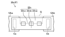
- FIG. 14 is a plan view showing a frame area of an organic EL display device according to another embodiment of the present invention.
- FIG. 15 is a plan view showing a frame area of a first modified example of the organic EL display device according to another embodiment of the present invention.
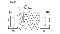
- FIG. 16 is a plan view showing a frame area of a second modified example of the organic EL display device according to the other embodiment of the present invention.
- First Embodiment 1 to 8 show a first embodiment of a display device according to the present invention.
- an organic EL display device provided with an organic EL element is illustrated as a display device provided with a light emitting element.
- FIG. 1 is a plan view of the organic EL display device 30a of the present embodiment.
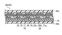
- FIG. 2 is a cross-sectional view of the display area D of the organic EL display device 30a along the line II-II in FIG.
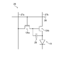
- FIG. 3 is an equivalent circuit diagram showing the TFT layer 29 constituting the organic EL display device 30a.
- FIG. 4 is a cross-sectional view showing the organic EL layer 16 constituting the organic EL display device 30a.
- FIG. 1 is a plan view of the organic EL display device 30a of the present embodiment.
- FIG. 2 is a cross-sectional view of the display area D of the organic EL display device 30a along the line II-II in FIG.
- FIG. 3 is an equivalent circuit diagram showing the TFT layer 29 constituting the
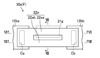
- FIG. 5 is a plan view showing the frame area of the organic EL display device 30a.
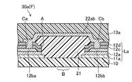
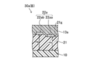
- 6, 7 and 8 are cross-sectional views of the frame region F of the organic EL display device 30 a taken along the lines VI-VI, VII-VII and VIII-VIII in FIG.
- the organic EL display device 30 a includes a display area D for displaying an image defined in a rectangular shape and a frame area F defined around the display area D.
- the organic EL elements 19 are provided, and a plurality of pixels are arranged in a matrix.
- a sub-pixel for performing red gradation display, a sub-pixel for performing green gradation display, and a sub-pixel for performing blue gradation display They are arranged side by side.
- a terminal portion T is provided at the right end of the frame area F in the drawing.
- a bent portion B which is bent at 180 ° (U-shape) with the longitudinal direction in the figure as an axis of bending. It is provided along one side (right side in the drawing) of the display area D.
- the organic EL display device 30a is provided as a light emitting element on the surface of the resin substrate layer 10, the TFT layer 29 provided on the surface of the resin substrate layer 10, and the TFT layer 29 in the display region D as shown in FIG.
- the organic EL element 19 is provided, a surface side protective layer 25 a provided on the surface of the organic EL element 19, and a back side protective layer 25 b provided on the back side of the resin substrate layer 10.
- the resin substrate layer 10 is made of, for example, a polyimide resin or the like having a thickness of about 10 ⁇ m to 20 ⁇ m, and is provided as a resin substrate.
- the TFT layer 29 includes a base coat film 11a provided on the resin substrate layer 10, a plurality of first TFTs 12ta (see FIG. 3) provided on the base coat film 11a, and a plurality of second TFTs 12tb.
- a TFT planarization film 13a is provided on each first TFT 12ta and each second TFT 12tb.
- a plurality of gate lines 26 are provided so as to extend parallel to each other in the lateral direction in the drawing.
- a plurality of source lines 27a are provided so as to extend in parallel to each other in the vertical direction in the figure.
- a plurality of power supply lines 27b are provided adjacent to the respective source lines 27a so as to extend in parallel in the vertical direction in the drawing. Further, in the TFT layer 29, as shown in FIG. 3, the first TFT 12ta, the second TFT 12tb, and the capacitor 28 are provided in each sub-pixel.
- the base coat film 11 a is formed of, for example, a single layer film or a laminated film of an inorganic insulating film such as silicon nitride, silicon oxide, or silicon oxynitride.
- the first TFT 12 ta is connected to the corresponding gate line 26 and source line 27 a in each sub-pixel.
- the second TFT 12 tb is connected to the corresponding first TFT 12 ta and the power supply line 27 b in each sub-pixel.
- the first TFT 12 ta and the second TFT 12 tb are, for example, a semiconductor layer provided in an island shape on the base coat film 11 a, a gate insulating film 12 a provided so as to cover the semiconductor layer (see FIG. 6), and a gate insulating film.
- a source electrode and a drain electrode are provided on the interlayer insulating film 12d and arranged to be separated from each other.
- the top gate type first TFT 12 ta and the second TFT 12 tb are illustrated in the present embodiment, the first TFT 12 ta and the second TFT 12 tb may be bottom gate type TFTs.
- the capacitor 28 is connected to the corresponding first TFT 12 ta and the power supply line 27 b in each sub-pixel as shown in FIG. 3.
- the capacitor 28 is, for example, one electrode formed in the same layer by the same material as the gate electrode, the other electrode formed in the same layer by the same material as the source electrode and the drain electrode, and a pair of them. It is comprised by the 1st interlayer insulation film 12c and / or the 2nd interlayer insulation film 12d (refer FIG. 6) provided between the electrodes.
- the TFT planarization film 13a is made of, for example, a colorless and transparent organic resin material such as a polyimide resin.
- the organic EL element 19 includes a plurality of first electrodes 14, an edge cover 15, a plurality of organic EL layers 16, a second electrode 17, and a sealing film sequentially provided on the TFT planarization film 13 a. It has eighteen.
- the plurality of first electrodes 14 are provided in a matrix on the TFT planarization film 13a so as to correspond to the plurality of sub-pixels.
- the first electrode 14 is connected to the drain electrode of each second TFT 12tb via a contact hole formed in the TFT planarization film 13a.
- the first electrode 14 has a function of injecting holes into the organic EL layer 16.
- the first electrode 14 is more preferably formed of a material having a large work function in order to improve the hole injection efficiency into the organic EL layer 16.
- the first electrode 14 for example, silver (Ag), aluminum (Al), vanadium (V), cobalt (Co), nickel (Ni), tungsten (W), gold (Au) , Calcium (Ca), titanium (Ti), yttrium (Y), sodium (Na), ruthenium (Ru), manganese (Mn), indium (In), magnesium (Mg), lithium (Li), ytterbium (Yb) And metal materials such as lithium fluoride (LiF).
- the material which comprises the 1st electrode 14 is magnesium (Mg) / copper (Cu), magnesium (Mg) / silver (Ag), sodium (Na) / potassium (K), astatine (At) / oxidation, for example Astatine (AtO 2 ), lithium (Li) / aluminum (Al), lithium (Li) / calcium (Ca) / aluminum (Al), or lithium fluoride (LiF) / calcium (Ca) / aluminum (Al), etc. It may be an alloy.
- the material constituting the first electrode 14 is, for example, a conductive oxide such as tin oxide (SnO), zinc oxide (ZnO), indium tin oxide (ITO), indium zinc oxide (IZO) or the like. It may be. Further, the first electrode 14 may be formed by laminating a plurality of layers made of the above materials. In addition, as a material with a large work function, indium tin oxide (ITO), indium zinc oxide (IZO), etc. are mentioned, for example.
- the edge cover 15 is provided in a lattice shape so as to cover the peripheral portion of each first electrode 14.
- silicon nitride SiN x (x is a positive number)
- silicon oxide SiO 2
- trisilicon tetranitride Si 3 N 4
- silicon oxynitride Inorganic films such as a ride (SiNO)
- organic films such as a polyimide resin, an acrylic resin, a polysiloxane resin, and a novolak resin, are mentioned.
- each organic EL layer 16 is disposed on the respective first electrodes 14 and provided in a matrix so as to correspond to the plurality of sub-pixels.
- each organic EL layer 16 is provided with a hole injection layer 1, a hole transport layer 2, a light emitting layer 3, an electron transport layer 4 and an electron injection sequentially provided on the first electrode 14.
- the layer 5 is provided.
- the hole injection layer 1 is also referred to as an anode buffer layer, and has the function of improving the hole injection efficiency from the first electrode 14 to the organic EL layer 16 by bringing the energy levels of the first electrode 14 and the organic EL layer 16 closer.
- the material constituting the hole injection layer for example, triazole derivative, oxadiazole derivative, imidazole derivative, polyarylalkane derivative, pyrazoline derivative, phenylenediamine derivative, oxazole derivative, styrylanthracene derivative, fluorenone derivative, Hydrazone derivatives, stilbene derivatives and the like can be mentioned.
- the hole transport layer 2 has a function of improving the transport efficiency of holes from the first electrode 14 to the organic EL layer 16.
- a material constituting the hole transport layer 2 for example, porphyrin derivative, aromatic tertiary amine compound, styrylamine derivative, polyvinylcarbazole, poly-p-phenylenevinylene, polysilane, triazole derivative, oxadiazole Derivative, imidazole derivative, polyarylalkane derivative, pyrazoline derivative, pyrazolone derivative, phenylenediamine derivative, arylamine derivative, amine-substituted chalcone derivative, oxazole derivative, styrylanthracene derivative, fluorenone derivative, hydrazone derivative, stilbene derivative, hydrogenated amorphous silicon, Hydrogenated amorphous silicon carbide, zinc sulfide, zinc selenide and the like can be mentioned.
- the light emitting layer 3 holes and electrons are injected from the first electrode 14 and the second electrode 17, respectively, and holes and electrons are recombined when a voltage is applied by the first electrode 14 and the second electrode 17. It is an area.
- the light emitting layer 3 is formed of a material having high light emission efficiency.
- a metal oxinoid compound [8-hydroxy quinoline metal complex], a naphthalene derivative, an anthracene derivative, a diphenyl ethylene derivative, a vinylacetone derivative, a triphenylamine derivative, a butadiene derivative, a coumarin derivative, for example , Benzoxazole derivative, oxadiazole derivative, oxazole derivative, benzimidazole derivative, thiadiazole derivative, benzthiazole derivative, styryl derivative, styrylamine derivative, bisstyrylbenzene derivative, trisstyrylbenzene derivative, perylene derivative, perinone derivative, aminopyrene derivative, Pyridine derivatives, rhodamine derivatives, aquidin derivatives, phenoxazone, quinacridone derivatives, rubrene, poly-p-phenylene vinylet , Polysilane, and the like.
- the electron transport layer 4 has a function of efficiently moving electrons to the light emitting layer 3.
- a material constituting the electron transport layer 4 for example, as an organic compound, oxadiazole derivative, triazole derivative, benzoquinone derivative, naphthoquinone derivative, anthraquinone derivative, tetracyanoanthraquinodimethane derivative, diphenoquinone derivative, fluorenone derivative And silole derivatives, metal oxinoid compounds and the like.
- the electron injection layer 5 has a function of bringing the energy levels of the second electrode 17 and the organic EL layer 16 closer to each other and improving the efficiency of injecting electrons from the second electrode 17 to the organic EL layer 16.
- the drive voltage of the organic EL element 19 can be lowered.
- the electron injection layer 5 is also called a cathode buffer layer.
- a material constituting the electron injection layer 5 for example, lithium fluoride (LiF), magnesium fluoride (MgF 2 ), calcium fluoride (CaF 2 ), strontium fluoride (SrF 2 ), barium fluoride Inorganic alkali compounds such as (BaF 2 ), aluminum oxide (Al 2 O 3 ), strontium oxide (SrO) and the like can be mentioned.
- the 2nd electrode 17 is provided so that each organic EL layer 16 and the edge cover 15 may be covered, as shown in FIG.
- the second electrode 17 has a function of injecting electrons into the organic EL layer 16.
- the second electrode 17 is more preferably made of a material having a small work function in order to improve the electron injection efficiency into the organic EL layer 16.
- the second electrode 17 for example, silver (Ag), aluminum (Al), vanadium (V), cobalt (Co), nickel (Ni), tungsten (W), gold (Au) , Calcium (Ca), titanium (Ti), yttrium (Y), sodium (Na), ruthenium (Ru), manganese (Mn), indium (In), magnesium (Mg), lithium (Li), ytterbium (Yb) And lithium fluoride (LiF).
- the second electrode 17 may be, for example, magnesium (Mg) / copper (Cu), magnesium (Mg) / silver (Ag), sodium (Na) / potassium (K), astatine (At) / oxide astatine (AtO 2) And lithium (Li) / aluminum (Al), lithium (Li) / calcium (Ca) / aluminum (Al), lithium fluoride (LiF) / calcium (Ca) / aluminum (Al), etc. May be
- the second electrode 17 may be formed of, for example, a conductive oxide such as tin oxide (SnO), zinc oxide (ZnO), indium tin oxide (ITO), indium zinc oxide (IZO), etc. .
- the second electrode 17 may be formed by laminating a plurality of layers made of the above materials.
- a material having a small work function for example, magnesium (Mg), lithium (Li), lithium fluoride (LiF), magnesium (Mg) / copper (Cu), magnesium (Mg) / silver (Ag), sodium (Na) / potassium (K), lithium (Li) / aluminum (Al), lithium (Li) / calcium (Ca) / aluminum (Al), lithium fluoride (LiF) / calcium (Ca) / aluminum (Al) Etc.
- the sealing film 18 is provided so as to cover the second electrode 17 as shown in FIG. 2 and has a function of protecting the organic EL layer 16 from moisture and oxygen.
- a material forming the sealing film 18 for example, silicon nitride (SiN x (SiN x) such as silicon oxide (SiO 2 ), aluminum oxide (Al 2 O 3 ), tetrasilicon nitride (Si 3 N 4 )) x is a positive number), inorganic materials such as silicon carbonitride (SiCN), and organic materials such as acrylate, polyurea, parylene, polyimide, and polyamide.
- the surface side protective layer 25a and the back surface side protective layer 25b are made of, for example, a polyimide resin having a thickness of about 2 ⁇ m.
- the resin substrate layer 10 provided on the surface of the resin substrate layer 10
- the inorganic laminated film A frame flattening film 21 provided so as to fill the opening A of La
- a plurality of frame wirings 22 a provided so as to extend parallel to each other on the surface of the inorganic laminated film La and the frame flattening film 21, and each frame And a TFT planarization film 13a provided so as to cover the wiring 22a.
- the inorganic laminated film La includes a base coat film 11a, a gate insulating film 12a, a first interlayer insulating film 12c, and a second interlayer insulating film 12d sequentially stacked on the resin substrate layer 10. ing. Further, as shown in FIGS. 6 and 7, the inorganic laminated film La is not provided in the bent portion B by having the opening portion A. Further, as shown in FIGS. 6 and 7, a first gate conductive layer 12ba and a second gate conductive layer 12bb are provided between the gate insulating film 12a and the first interlayer insulating film 12c of the inorganic laminated film La. There is.
- the first gate conductive layer 12 ba is connected to the signal wiring (gate line, source line, power supply line, etc.) of the organic EL element 19 in the display area D.
- the second gate conductive layer 12bb is provided to extend to the terminal portion T.
- the front surface side protective layer 25a and the rear surface side protective layer 25b disposed in the display area D are also provided in most of the frame area F, but are not provided in the bent portion B of the frame area F. .
- the frame flattening film 21a is made of, for example, an organic insulating film such as a polyimide resin having a thickness of about 2 ⁇ m.
- the frame wiring 22a is provided between the frame flattening film 21 and the TFT flat film 13a in the bending portion B, as shown in FIGS. 5 to 8, and the first branch wiring 22aa and the first branch wiring 22aa branched into two are provided.
- a second branch wiring 22ab is provided. Further, as shown in FIGS. 5 to 7, both ends of the frame wiring 22a are the first gate conductive layer via contact holes Ca and Cb formed in the first interlayer insulating film 12c and the second interlayer insulating film 12d. It is connected to 12ba and the 2nd gate electric conduction layer 12bb, respectively.
- the frame wiring 22a is formed of, for example, a metal laminated film such as titanium film (about 200 nm thick) / aluminum film (about 100 nm thick) / titanium film (about 200 nm thick).
- the frame wiring 22a formed of a metal laminated film is illustrated, but the frame wiring 22a may be formed of a metal single layer film.
- the frame wiring 22a provided with the first branch wiring 22aa and the second branch wiring 22ab branched into two is illustrated, but the frame wiring 22a may be branched into three or more.
- the frame wiring 22a connected to the first gate conductive layer 12ba and the second gate conductive layer 12bb is illustrated in the present embodiment, the frame wiring 22a may be connected to the conductive layers of other layers. .
- the first branch wiring 22aa is provided so as to pass through the inside of the groove 21g formed on the surface of the frame flattening film 21, as shown in FIG. 5, FIG. 6, and FIG. Further, as shown in FIGS. 5, 7 and 8, the second branch wiring 22ab is provided outside the groove 21g formed on the surface of the frame flattening film 21. Therefore, as shown in FIG. 8, the first branch wiring 22aa is provided at a height Ha (for example, about 0.25 ⁇ m to 1.5 ⁇ m) from the surface of the resin substrate layer 10, and the second branch wiring 22ab is a resin It is provided at a height Hb (for example, about 0.5 ⁇ m to about 3.0 ⁇ m) from the surface of the substrate layer 10.
- a height Ha for example, about 0.25 ⁇ m to 1.5 ⁇ m
- Hb for example, about 0.5 ⁇ m to about 3.0 ⁇ m
- the organic EL display device 30a described above has flexibility, and in each sub-pixel, the light emitting layer 3 of the organic EL layer 16 is appropriately caused to emit light through the first TFT 12ta and the second TFT 12tb to perform image display. It is configured.
- the organic EL display device 30a of the present embodiment can be manufactured as follows.
- the base coat film 11a and the organic EL element 19 are formed on the surface of the resin substrate layer 10 formed on the glass substrate using a known method, and the surface side protective layer is formed on the organic EL element 19 via the adhesive layer. After sticking 25a, it can manufacture by sticking the back surface side protective layer 25b through the adhesive layer on the back surface of the resin substrate layer 10 which made the glass substrate peel.
- the frame wiring 22 of the frame area F is formed when forming the source electrode and the drain electrode of the first TFT 12 ta (second TFT 12 tb) that constitutes the organic EL element 19.
- the frame flattening film 21 of the frame area F is a photosensitive organic compound such as polyimide resin only in the frame area F before the source electrode and drain electrode of the first TFT 12 ta (second TFT 12 tb) constituting the organic EL element 19 are formed.
- the insulating film is formed and formed by patterning using a halftone mask, a gray tone mask, or the like.
- the frame wiring 22a is provided with the first branch wiring 22aa and the second branch wiring 22ab branched into two at the bending portion B, and the first branch wiring 22aa and the second branch wiring 22ab are disposed at different heights Ha and Hb relative to the resin substrate layer 10. Therefore, when the bent portion B is bent, the stresses applied to the first branch wiring 22aa and the second branch wiring 22ab are different from each other. As a result, when the bent portion B is bent, it is suppressed that the first branch wiring 22aa and the second branch wiring 22ab are uniformly disconnected. Therefore, the first branch that is branched at the bent portion B of the frame area F It is possible to suppress the disconnection of the wiring 22aa and the second branch wiring 22ab.
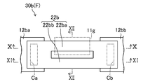
- FIG. 9 is a plan view showing the frame area F of the organic EL display device 30b of the present embodiment.
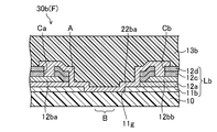
- 10, 11 and 12 are cross-sectional views of the frame area F of the organic EL display device 30b taken along the lines XX, XI-XI and XII-XII in FIG.
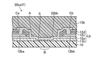
- FIG. 13 is a cross-sectional view showing a frame area F of an organic EL display device 30ba which is a modification of the organic EL display device 30b, and is a view corresponding to FIG.
- the same parts as those in FIGS. 1 to 8 are assigned the same reference numerals and detailed explanations thereof will be omitted.
- the organic EL display device 30a in which the step is formed between the first branch wiring 22aa and the second branch wiring 22ab by using the groove 21g of the frame flattening film 21 is exemplified.
- the organic EL display device 30b in which a step is formed between the first branch wiring 22ba and the second branch wiring 22bb by using the groove 11g of the base coat film 11b is illustrated.
- the organic EL display device 30b has a display region D for displaying an image defined in a rectangular shape and a frame region F defined around the display region D. And have.
- the display area D of the organic EL display device 30 b has a configuration similar to that of the organic EL display device 30 a of the first embodiment.
- the resin substrate layer 10 in the frame area F, the resin substrate layer 10, the inorganic laminated film Lb provided on the surface of the resin substrate layer 10, and the inorganic laminated film
- a frame wiring 22b is provided on the surface of Lb so as to extend in parallel with each other, and a TFT planarization film 13b is provided to cover each frame wiring 22b.
- the inorganic laminated film Lb includes a base coat film 11b, a gate insulating film 12a, a first interlayer insulating film 12c, and a second interlayer insulating film 12d sequentially stacked on the resin substrate layer 10. ing.
- the gate insulating film 12a, the first interlayer insulating film 12c, and the second interlayer insulating film 12d of the inorganic laminated film Lb are provided in the bent portion B by having the opening A as shown in FIGS. 10 and 11. It is not done. Further, as shown in FIGS.
- a first gate conductive layer 12ba and a second gate conductive layer 12bb are provided between the gate insulating film 12a and the first interlayer insulating film 12c of the inorganic laminated film Lb.
- the front surface side protective layer 25a and the rear surface side protective layer 25b disposed in the display area D are also provided in most of the frame area F, but are not provided in the bent portion B of the frame area F. .
- the frame wiring 22b is provided between the base coat film 11b and the TFT planarization film 13b at the bending portion B as shown in FIGS. 9 to 12, and the first branch wiring 22ba and the second branch wiring 22b branched into two are provided.
- a 2-branch wiring 22bb is provided. Further, as shown in FIGS. 9 to 11, both ends of the frame wiring 22b are the first gate conductive layer via contact holes Ca and Cb formed in the first interlayer insulating film 12c and the second interlayer insulating film 12d. It is connected to 12ba and the 2nd gate electric conduction layer 12bb, respectively.
- the frame wiring 22b is formed of, for example, a metal laminated film such as titanium film (about 200 nm thick) / aluminum film (about 100 nm thick) / titanium film (about 200 nm thick).
- a metal laminated film such as titanium film (about 200 nm thick) / aluminum film (about 100 nm thick) / titanium film (about 200 nm thick).
- the frame wiring 22b formed of a metal laminated film is illustrated, but the frame wiring 22b may be formed of a metal single layer film.
- the frame wiring 22b including the first branch wiring 22ba and the second branch wiring 22bb branched into two is illustrated, but the frame wiring 22b may be branched into three or more.
- the first branch wiring 22ba is provided so as to pass through the inside of the groove 11g formed on the surface of the base coat film 11b, as shown in FIGS.
- the groove 11g is provided so as to penetrate the base coat film 11b.
- the second branch wiring 22bb is provided outside the groove 11g formed on the surface of the base coat film 11b. Therefore, as shown in FIG. 12, the first branch wiring 22ba is provided on the surface of the resin substrate layer 10, and the second branch wiring 22bb has a height Hb (for example, 0.1 ⁇ m to about) from the surface of the resin substrate layer 10. (About 0.5 ⁇ m).
- Hb for example, 0.1 ⁇ m to about
- the base coat film 11b is formed thinner at the bent portion B where the second branch wiring 22bb is disposed than at the portion of the display area D, so the second branch wiring 22bb is broken. Can be suppressed.
- the thinly formed portion of the base coat film 11 b at the bent portion B is formed with a plurality of slits S in order to suppress the occurrence of cracks. It may be divided into a plurality.
- the organic EL display device 30 b described above has flexibility, and in each sub-pixel, the organic EL layer 16 is formed via the first TFT 12 ta and the second TFT 12 tb. By appropriately emitting light from the light emitting layer 3, an image is displayed.
- the organic EL display device 30b changes the pattern shape of the base coat film 11a using a halftone mask, a gray tone mask, or the like. , Can be manufactured.
- the first branch wiring 22b includes the first branch wiring 22ba and the second branch wiring 22bb in which the frame wiring 22b is branched into two at the bending portion B. 22ba and the second branch wiring 22bb are arranged at different heights with respect to the resin substrate layer 10. Therefore, when the bent portion B is bent, stresses applied to the first branch wiring 22ba and the second branch wiring 22bb are different from each other. Thereby, when the bent portion B is bent, it is suppressed that the first branch wiring 22ba and the second branch wiring 22bb are uniformly disconnected. Therefore, the first branch that is branched at the bending portion B of the frame region F It is possible to suppress the disconnection of the wiring 22ba and the second branch wiring 22bb.
- FIGS. 14 to 16 are plan views showing the frame area F of the organic EL display devices 30c to 30e of the present embodiment.
- the first branch wiring 22ca and the second branch wiring 22cb constituting the frame wiring 22c are formed by the connecting portions 22cc formed at two positions in the middle portion thereof. It is connected.
- a step is formed using a groove G formed on the surface of a base coat film, a frame flattening film or the like.
- the connecting portion 22 cc is provided to get over the step G due to the two types of heights.
- the first branch wiring 22da and the second branch wiring 22db constituting the frame wiring 22d are diagonally connected by the connection portion 22dc formed in the middle portion thereof.
- a step is formed between the first branch wiring 22da and the second branch wiring 22db using a groove G formed on the surface of a base coat film, a frame flattening film, or the like.
- the connecting portion 22dc is provided to get over the step G due to the two types of heights.
- the first branch wiring 22ea and the second branch wiring 22eb constituting the frame wiring 22e are connected by the connection portions 22ec formed at a plurality of locations in the middle portion thereof. ing.
- the frame wiring 22e is provided in a chain shape in plan view.
- a step is formed between the first branch wiring 22ea and the second branch wiring 22eb using a groove G formed on the surface of the base coat film, the frame flattening film, or the like.
- the connection portion 22 ec is provided to get over the step G due to the two types of heights.
- the organic EL display device is exemplified as the display device, but the present invention is a display device including a plurality of light emitting elements driven by current, for example, a light emitting element using a quantum dot containing layer
- the present invention can be applied to a display device equipped with a QLED (Quantum-dot light emitting diode).
- the organic EL layer having a five-layer laminated structure of the hole injection layer, the hole transport layer, the light emitting layer, the electron transport layer, and the electron injection layer is exemplified. It may be a three-layer laminated structure of a hole injection layer and hole transport layer, a light emitting layer, and an electron transport layer and electron injection layer.
- the organic EL display device is exemplified in which the first electrode is an anode and the second electrode is a cathode.
- the laminated structure of the organic EL layer is reversed and the first electrode is a cathode.
- the present invention can also be applied to an organic EL display device in which the second electrode is an anode.
- the organic EL display device in which the electrode of the TFT connected to the first electrode is the drain electrode is exemplified.
- the electrode of the TFT connected to the first electrode is the source electrode
- the present invention can also be applied to an organic EL display device to be called.
- the present invention is useful for flexible display devices.
Landscapes
- Engineering & Computer Science (AREA)
- Microelectronics & Electronic Packaging (AREA)
- Physics & Mathematics (AREA)
- Optics & Photonics (AREA)
- General Physics & Mathematics (AREA)
- Theoretical Computer Science (AREA)
- Electroluminescent Light Sources (AREA)
- Devices For Indicating Variable Information By Combining Individual Elements (AREA)
Abstract
額縁領域(F)に設けられた額縁配線(22a)は、折り曲げ部において、複数に分岐した複数の分岐配線(22aa、22ab)を備え、複数の分岐配線(22aa、22ab)は、樹脂基板に対して、少なくとも2種類の高さに配置されている。
Description
本発明は、表示装置に関するものである。
近年、液晶表示装置に代わる表示装置として、有機EL(electroluminescence)素子を用いた自発光型の有機EL表示装置が注目されている。この有機EL表示装置では、可撓性を有する樹脂基板上に有機EL素子や種々のフィルム等が積層されたフレキシブルな有機EL表示装置が提案されている。ここで、有機EL表示装置では、画像表示を行う矩形状の表示領域と、その表示領域の周囲に額縁領域とが設けられ、額縁領域を縮小させることが要望されている。そして、フレキシブルな有機EL表示装置では、例えば、端子側の額縁領域を折り曲げることにより、額縁領域を縮小させると、その額縁領域に配置された配線が断線するおそれがある。
例えば、特許文献1には、互いにおよそ180度位相がずれた一対の正弦波形の金属配線からなる冗長性デザインを備えたフレキシブルディスプレイが開示されている。
ところで、額縁領域の折り曲げ部において、上記特許文献1のように、配線を複数に分岐して冗長化すると、分岐した複数の配線の一部が断線しても、配線の機能が維持されるものの、折り曲げ部を折り曲げた際に、分岐した複数の配線に一様な応力が加わり易いので、分岐した複数の配線が一様に断線するおそれがあるので、改善の余地がある。
本発明は、かかる点に鑑みてなされたものであり、その目的とするところは、額縁領域の折り曲げ部において、分岐した配線の断線を抑制することにある。
上記目的を達成するために、本発明に係る表示装置は、樹脂基板と、上記樹脂基板上に設けられた表示領域を構成する発光素子と、上記表示領域の周囲に設けられた額縁領域と、上記額縁領域の端部に設けられた端子部と、上記表示領域及び端子部の間に設けられた折り曲げ部と、上記額縁領域に設けられ、上記発光素子に接続されて上記端子部に延びる額縁配線とを備えた表示装置であって、上記額縁配線は、上記折り曲げ部において、複数に分岐した複数の分岐配線を備え、上記複数の分岐配線は、上記樹脂基板に対して、少なくとも2種類の高さに配置されていることを特徴とする。
本発明によれば、額縁配線が折り曲げ部において複数に分岐した複数の分岐配線を備え、複数の分岐配線が樹脂基板に対して少なくとも2種類の高さに配置されているので、額縁領域の折り曲げ部において、分岐した配線の断線を抑制することができる。
以下、本発明の実施形態を図面に基づいて詳細に説明する。なお、本発明は、以下の各実施形態に限定されるものではない。
《第1の実施形態》
図1~図8は、本発明に係る表示装置の第1の実施形態を示している。なお、以下の各実施形態では、発光素子を備えた表示装置として、有機EL素子を備えた有機EL表示装置を例示する。ここで、図1は、本実施形態の有機EL表示装置30aの平面図である。また、図2は、図1中のII-II線に沿った有機EL表示装置30aの表示領域Dの断面図である。また、図3は、有機EL表示装置30aを構成するTFT層29を示す等価回路図である。また、図4は、有機EL表示装置30aを構成する有機EL層16を示す断面図である。また、図5は、有機EL表示装置30aの額縁領域を示す平面図である。また、図6、図7及び図8は、図5中のVI-VI線、VII-VII線及びVIII-VIII線に沿った有機EL表示装置30aの額縁領域Fの断面図である。
図1~図8は、本発明に係る表示装置の第1の実施形態を示している。なお、以下の各実施形態では、発光素子を備えた表示装置として、有機EL素子を備えた有機EL表示装置を例示する。ここで、図1は、本実施形態の有機EL表示装置30aの平面図である。また、図2は、図1中のII-II線に沿った有機EL表示装置30aの表示領域Dの断面図である。また、図3は、有機EL表示装置30aを構成するTFT層29を示す等価回路図である。また、図4は、有機EL表示装置30aを構成する有機EL層16を示す断面図である。また、図5は、有機EL表示装置30aの額縁領域を示す平面図である。また、図6、図7及び図8は、図5中のVI-VI線、VII-VII線及びVIII-VIII線に沿った有機EL表示装置30aの額縁領域Fの断面図である。
有機EL表示装置30aは、図1に示すように、矩形状に規定された画像表示を行う表示領域Dと、表示領域Dの周囲に規定された額縁領域Fとを備えている。ここで、有機EL表示装置30aの表示領域Dには、図2に示すように、有機EL素子19が設けられていると共に、複数の画素がマトリクス状に配列されている。なお、表示領域Dの各画素では、例えば、赤色の階調表示を行うためのサブ画素、緑色の階調表示を行うためのサブ画素、及び青色の階調表示を行うためのサブ画素が互いに隣り合うように配列されている。また、額縁領域Fの図中右端部には、図1に示すように、端子部Tが設けられている。また、額縁領域Fにおいて、表示領域D及び端子部Tの間には、図1に示すように、図中縦方向を折り曲げの軸として180°に(U字状に)折り曲げられる折り曲げ部Bが表示領域Dの一辺(図中右辺)に沿うように設けられている。
有機EL表示装置30aは、図2に示すように、表示領域Dにおいて、樹脂基板層10と、樹脂基板層10の表面に設けられたTFT層29と、TFT層29の表面に発光素子として設けられた有機EL素子19と、有機EL素子19の表面に設けられた表面側保護層25aと、樹脂基板層10の裏面に設けられた裏面側保護層25bとを備えている。
樹脂基板層10は、例えば、厚さ10μm~20μm程度のポリイミド樹脂等により構成され、樹脂基板として設けられている。
TFT層29は、図2に示すように、樹脂基板層10上に設けられたベースコート膜11aと、ベースコート膜11a上に設けられた複数の第1TFT12ta(図3参照)及び複数の第2TFT12tbと、各第1TFT12ta及び各第2TFT12tb上に設けられたTFT平坦化膜13aとを備えている。ここで、TFT層29では、図3に示すように、図中横方向に互いに平行に延びるように複数のゲート線26が設けられている。また、TFT層29では、図3に示すように、図中縦方向に互いに平行に延びるように複数のソース線27aが設けられている。また、TFT層29では、図3に示すように、各ソース線27aと隣り合って、図中縦方向に互いに平行に延びるように複数の電源線27bが設けられている。また、TFT層29では、図3に示すように、各サブ画素において、第1TFT12ta、第2TFT12tb及びキャパシタ28が設けられている。
ベースコート膜11aは、例えば、窒化シリコン、酸化シリコン、酸窒化シリコン等の無機絶縁膜の単層膜又は積層膜により構成されている。
第1TFT12taは、図3に示すように、各サブ画素において、対応するゲート線26及びソース線27aに接続されている。また、第2TFT12tbは、図3に示すように、各サブ画素において、対応する第1TFT12ta及び電源線27bに接続されている。ここで、第1TFT12ta及び第2TFT12tbは、例えば、ベースコート膜11a上に島状に設けられた半導体層と、半導体層を覆うように設けられたゲート絶縁膜12a(図6参照)と、ゲート絶縁膜12a上に半導体層の一部と重なるように設けられたゲート電極と、ゲート電極を覆うように設けられた第1層間絶縁膜12c及び第2層間絶縁膜12d(図6参照)と、第2層間絶縁膜12d上に設けられ、互いに離間するように配置されたソース電極及びドレイン電極とを備えている。なお、本実施形態では、トップゲート型の第1TFT12ta及び第2TFT12tbを例示したが、第1TFT12ta及び第2TFT12tbは、ボトムゲート型のTFTであってもよい。
キャパシタ28は、図3に示すように、各サブ画素において、対応する第1TFT12ta及び電源線27bに接続されている。ここで、キャパシタ28は、例えば、ゲート電極と同一材料により同一層に形成された一方の電極と、ソース電極及びドレイン電極と同一材料により同一層に形成された他方の電極と、それらの一対の電極の間に設けられた第1層間絶縁膜12c及び/又は第2層間絶縁膜12d(図6参照)とにより構成されている。
TFT平坦化膜13aは、例えば、ポリイミド樹脂等の無色透明な有機樹脂材料により構成されている。
有機EL素子19は、図2に示すように、TFT平坦化膜13a上に順に設けられた複数の第1電極14、エッジカバー15、複数の有機EL層16、第2電極17及び封止膜18を備えている。
複数の第1電極14は、図2に示すように、複数のサブ画素に対応するように、TFT平坦化膜13a上にマトリクス状に設けられている。ここで、第1電極14は、図2に示すように、TFT平坦化膜13aに形成されたコンタクトホールを介して、各第2TFT12tbのドレイン電極に接続されている。また、第1電極14は、有機EL層16にホール(正孔)を注入する機能を有している。また、第1電極14は、有機EL層16への正孔注入効率を向上させるために、仕事関数の大きな材料で形成するのがより好ましい。ここで、第1電極14を構成する材料としては、例えば、銀(Ag)、アルミニウム(Al)、バナジウム(V)、コバルト(Co)、ニッケル(Ni)、タングステン(W)、金(Au)、カルシウム(Ca)、チタン(Ti)、イットリウム(Y)、ナトリウム(Na)、ルテニウム(Ru)、マンガン(Mn)、インジウム(In)、マグネシウム(Mg)、リチウム(Li)、イッテルビウム(Yb)、フッ化リチウム(LiF)等の金属材料が挙げられる。また、第1電極14を構成する材料は、例えば、マグネシウム(Mg)/銅(Cu)、マグネシウム(Mg)/銀(Ag)、ナトリウム(Na)/カリウム(K)、アスタチン(At)/酸化アスタチン(AtO2)、リチウム(Li)/アルミニウム(Al)、リチウム(Li)/カルシウム(Ca)/アルミニウム(Al)、又はフッ化リチウム(LiF)/カルシウム(Ca)/アルミニウム(Al)等の合金であっても構わない。さらに、第1電極14を構成する材料は、例えば、酸化スズ(SnO)、酸化亜鉛(ZnO)、インジウムスズ酸化物(ITO)、インジウム亜鉛酸化物(IZO)のような導電性酸化物等であってもよい。また、第1電極14は、上記材料からなる層を複数積層して形成されていてもよい。なお、仕事関数の大きな材料としては、例えば、インジウムスズ酸化物(ITO)やインジウム亜鉛酸化物(IZO)等が挙げられる。
エッジカバー15は、図2に示すように、各第1電極14の周縁部を覆うように格子状に設けられている。ここで、エッジカバー15を構成する材料としては、例えば、酸化シリコン(SiO2)、四窒化三ケイ素(Si3N4)のような窒化シリコン(SiNx(xは正数))、シリコンオキシナイトライド(SiNO)等の無機膜、又はポリイミド樹脂、アクリル樹脂、ポリシロキサン樹脂、ノボラック樹脂等の有機膜が挙げられる。
複数の有機EL層16は、図2に示すように、各第1電極14上に配置され、複数のサブ画素に対応するように、マトリクス状に設けられている。ここで、各有機EL層16は、図4に示すように、第1電極14上に順に設けられた正孔注入層1、正孔輸送層2、発光層3、電子輸送層4及び電子注入層5を備えている。
正孔注入層1は、陽極バッファ層とも呼ばれ、第1電極14と有機EL層16とのエネルギーレベルを近づけ、第1電極14から有機EL層16への正孔注入効率を改善する機能を有している。ここで、正孔注入層1を構成する材料としては、例えば、トリアゾール誘導体、オキサジアゾール誘導体、イミダゾール誘導体、ポリアリールアルカン誘導体、ピラゾリン誘導体、フェニレンジアミン誘導体、オキサゾール誘導体、スチリルアントラセン誘導体、フルオレノン誘導体、ヒドラゾン誘導体、スチルベン誘導体等が挙げられる。
正孔輸送層2は、第1電極14から有機EL層16への正孔の輸送効率を向上させる機能を有している。ここで、正孔輸送層2を構成する材料としては、例えば、ポルフィリン誘導体、芳香族第三級アミン化合物、スチリルアミン誘導体、ポリビニルカルバゾール、ポリ-p-フェニレンビニレン、ポリシラン、トリアゾール誘導体、オキサジアゾール誘導体、イミダゾール誘導体、ポリアリールアルカン誘導体、ピラゾリン誘導体、ピラゾロン誘導体、フェニレンジアミン誘導体、アリールアミン誘導体、アミン置換カルコン誘導体、オキサゾール誘導体、スチリルアントラセン誘導体、フルオレノン誘導体、ヒドラゾン誘導体、スチルベン誘導体、水素化アモルファスシリコン、水素化アモルファス炭化シリコン、硫化亜鉛、セレン化亜鉛等が挙げられる。
発光層3は、第1電極14及び第2電極17による電圧印加の際に、第1電極14及び第2電極17から正孔及び電子がそれぞれ注入されると共に、正孔及び電子が再結合する領域である。ここで、発光層3は、発光効率が高い材料により形成されている。そして、発光層3を構成する材料としては、例えば、金属オキシノイド化合物[8-ヒドロキシキノリン金属錯体]、ナフタレン誘導体、アントラセン誘導体、ジフェニルエチレン誘導体、ビニルアセトン誘導体、トリフェニルアミン誘導体、ブタジエン誘導体、クマリン誘導体、ベンズオキサゾール誘導体、オキサジアゾール誘導体、オキサゾール誘導体、ベンズイミダゾール誘導体、チアジアゾール誘導体、ベンズチアゾール誘導体、スチリル誘導体、スチリルアミン誘導体、ビススチリルベンゼン誘導体、トリススチリルベンゼン誘導体、ペリレン誘導体、ペリノン誘導体、アミノピレン誘導体、ピリジン誘導体、ローダミン誘導体、アクイジン誘導体、フェノキサゾン、キナクリドン誘導体、ルブレン、ポリ-p-フェニレンビニレン、ポリシラン等が挙げられる。
電子輸送層4は、電子を発光層3まで効率良く移動させる機能を有している。ここで、電子輸送層4を構成する材料としては、例えば、有機化合物として、オキサジアゾール誘導体、トリアゾール誘導体、ベンゾキノン誘導体、ナフトキノン誘導体、アントラキノン誘導体、テトラシアノアントラキノジメタン誘導体、ジフェノキノン誘導体、フルオレノン誘導体、シロール誘導体、金属オキシノイド化合物等が挙げられる。
電子注入層5は、第2電極17と有機EL層16とのエネルギーレベルを近づけ、第2電極17から有機EL層16へ電子が注入される効率を向上させる機能を有し、この機能により、有機EL素子19の駆動電圧を下げることができる。なお、電子注入層5は、陰極バッファ層とも呼ばれる。ここで、電子注入層5を構成する材料としては、例えば、フッ化リチウム(LiF)、フッ化マグネシウム(MgF2)、フッ化カルシウム(CaF2)、フッ化ストロンチウム(SrF2)、フッ化バリウム(BaF2)のような無機アルカリ化合物、酸化アルミニウム(Al2O3)、酸化ストロンチウム(SrO)等が挙げられる。
第2電極17は、図2に示すように、各有機EL層16及びエッジカバー15を覆うように設けられている。また、第2電極17は、有機EL層16に電子を注入する機能を有している。また、第2電極17は、有機EL層16への電子注入効率を向上させるために、仕事関数の小さな材料で構成するのがより好ましい。ここで、第2電極17を構成する材料としては、例えば、銀(Ag)、アルミニウム(Al)、バナジウム(V)、コバルト(Co)、ニッケル(Ni)、タングステン(W)、金(Au)、カルシウム(Ca)、チタン(Ti)、イットリウム(Y)、ナトリウム(Na)、ルテニウム(Ru)、マンガン(Mn)、インジウム(In)、マグネシウム(Mg)、リチウム(Li)、イッテルビウム(Yb)、フッ化リチウム(LiF)等が挙げられる。また、第2電極17は、例えば、マグネシウム(Mg)/銅(Cu)、マグネシウム(Mg)/銀(Ag)、ナトリウム(Na)/カリウム(K)、アスタチン(At)/酸化アスタチン(AtO2)、リチウム(Li)/アルミニウム(Al)、リチウム(Li)/カルシウム(Ca)/アルミニウム(Al)、フッ化リチウム(LiF)/カルシウム(Ca)/アルミニウム(Al)等の合金により形成されていてもよい。また、第2電極17は、例えば、酸化スズ(SnO)、酸化亜鉛(ZnO)、インジウムスズ酸化物(ITO)、インジウム亜鉛酸化物(IZO)等の導電性酸化物により形成されていてもよい。また、第2電極17は、上記材料からなる層を複数積層して形成されていてもよい。なお、仕事関数が小さい材料としては、例えば、マグネシウム(Mg)、リチウム(Li)、フッ化リチウム(LiF)、マグネシウム(Mg)/銅(Cu)、マグネシウム(Mg)/銀(Ag)、ナトリウム(Na)/カリウム(K)、リチウム(Li)/アルミニウム(Al)、リチウム(Li)/カルシウム(Ca)/アルミニウム(Al)、フッ化リチウム(LiF)/カルシウム(Ca)/アルミニウム(Al)等が挙げられる。
封止膜18は、図2に示すように、第2電極17を覆うように設けられ、有機EL層16を水分や酸素から保護する機能を有している。ここで、封止膜18を構成する材料としては、例えば、酸化シリコン(SiO2)や酸化アルミニウム(Al2O3)、四窒化三ケイ素(Si3N4)のような窒化シリコン(SiNx(xは正数))、炭窒化ケイ素(SiCN)等の無機材料、アクリレート、ポリ尿素、パリレン、ポリイミド、ポリアミド等の有機材料が挙げられる。
表面側保護層25a及び裏面側保護層25bは、例えば、厚さ2μm程度のポリイミド樹脂等により構成されている。
有機EL表示装置30aは、図5、図6及び図7に示すように、額縁領域Fにおいて、樹脂基板層10と、樹脂基板層10の表面に設けられた無機積層膜Laと、無機積層膜Laの開口部Aを埋めるように設けられた額縁平坦化膜21と、無機積層膜La及び額縁平坦化膜21の表面に互いに平行に延びるように設けられた複数の額縁配線22aと、各額縁配線22aを覆うように設けられたTFT平坦化膜13aとを備えている。
無機積層膜Laは、図6及び図7に示すように、樹脂基板層10上に順に積層されたベースコート膜11a、ゲート絶縁膜12a、第1層間絶縁膜12c及び第2層間絶縁膜12dを備えている。また、無機積層膜Laは、図6及び図7に示すように、開口部Aを有することにより、折り曲げ部Bに設けられていない。また、無機積層膜Laのゲート絶縁膜12a及び第1層間絶縁膜12cの間には、図6及び図7に示すように、第1ゲート導電層12ba及び第2ゲート導電層12bbが設けられている。ここで、第1ゲート導電層12baは、表示領域Dの有機EL素子19の信号配線(ゲート線、ソース線、電源線等)に接続されている。また、第2ゲート導電層12bbは、端子部Tに延びるように設けられている。なお、表示領域Dに配置された表面側保護層25a及び裏面側保護層25bは、額縁領域Fの大部分にも設けられているが、額縁領域Fの折り曲げ部Bには、設けられていない。
額縁平坦化膜21aは、例えば、厚さ2μm程度のポリイミド樹脂等の有機絶縁膜により構成されている。
額縁配線22aは、図5~図8に示すように、折り曲げ部Bにおいて、額縁平坦化膜21及びTFT平坦膜13aの間に挟まれて設けられ、2つに分岐した第1分岐配線22aa及び第2分岐配線22abを備えている。また、額縁配線22aの両端部は、図5~図7に示すように、第1層間絶縁膜12c及び第2層間絶縁膜12dに形成されたコンタクトホールCa及びCbを介して第1ゲート導電層12ba及び第2ゲート導電層12bbにそれぞれ接続されている。また、額縁配線22aは、例えば、チタン膜(厚さ200nm程度)/アルミニウム膜(厚さ100nm程度)/チタン膜(厚さ200nm程度)等の金属積層膜により構成されている。なお、本実施形態では、金属積層膜により構成された額縁配線22aを例示したが、額縁配線22aは、金属単層膜により構成されていてもよい。また、本実施形態では、2つに分岐した第1分岐配線22aa及び第2分岐配線22abを備えた額縁配線22aを例示したが、額縁配線22aは、3つ以上に分岐していてもよい。また、本実施形態では、第1ゲート導電層12ba及び第2ゲート導電層12bbに接続された額縁配線22aを例示したが、額縁配線22aは、その他の層の導電層に接続されていてもよい。
第1分岐配線22aaは、図5、図6及び図8に示すように、額縁平坦化膜21の表面に形成された溝21gの内部を通るように設けられている。また、第2分岐配線22abは、図5、図7及び図8に示すように、額縁平坦化膜21の表面に形成された溝21gの外部に設けられている。そのため、図8に示すように、第1分岐配線22aaは、樹脂基板層10の表面から高さHa(例えば、0.25μm~1.5μm程度)に設けられ、第2分岐配線22abは、樹脂基板層10の表面から高さHb(例えば、0.5μm~3.0μm程度)に設けられている。
上述した有機EL表示装置30aは、可撓性を有し、各サブ画素において、第1TFT12ta及び第2TFT12tbを介して有機EL層16の発光層3を適宜発光させることにより、画像表示を行うように構成されている。
本実施形態の有機EL表示装置30aは、以下のようにして製造することができる。
例えば、ガラス基板上に形成した樹脂基板層10の表面に、周知の方法を用いて、ベースコート膜11a及び有機EL素子19を形成し、有機EL素子19上に接着層を介して表面側保護層25aを貼り付けた後に、ガラス基板を剥離させた樹脂基板層10の裏面に接着層を介して裏面側保護層25bを貼り付けることにより、製造することができる。ここで、額縁領域Fの額縁配線22は、有機EL素子19を構成する第1TFT12ta(第2TFT12tb)のソース電極及びドレイン電極を形成する際に形成される。また、額縁領域Fの額縁平坦化膜21は、有機EL素子19を構成する第1TFT12ta(第2TFT12tb)のソース電極及びドレイン電極を形成する前に、額縁領域Fだけにポリイミド樹脂等の感光性有機絶縁膜を成膜して、ハーフトーンマスクやグレートーンマスク等を用いてパターニングすることにより形成される。
以上説明したように、本実施形態の有機EL表示装置30aによれば、額縁配線22aが折り曲げ部Bにおいて2つに分岐した第1分岐配線22aa及び第2分岐配線22abを備え、第1分岐配線22aa及び第2分岐配線22abが樹脂基板層10に対して異なる高さHa及びHbに配置されている。そのため、折り曲げ部Bを折り曲げた際に、第1分岐配線22aa及び第2分岐配線22abに加わる応力が互いに異なることになる。これにより、折り曲げ部Bを折り曲げた際に、第1分岐配線22aa及び第2分岐配線22abが一様に断線することが抑制されるので、額縁領域Fの折り曲げ部Bにおいて、分岐した第1分岐配線22aa及び第2分岐配線22abの断線を抑制することができる。
《第2の実施形態》
図9~図13は、本発明に係る表示装置の第2の実施形態を示している。ここで、図9は、本実施形態の有機EL表示装置30bの額縁領域Fを示す平面図である。また、図10、図11及び図12は、図9中のX-X線、XI-XI線及びXII-XII線に沿った有機EL表示装置30bの額縁領域Fの断面図である。また、図13は、有機EL表示装置30bの変形例である有機EL表示装置30baの額縁領域Fを示す断面図であり、図11に相当する図である。なお、以下の各実施形態において、図1~図8と同じ部分については同じ符号を付して、その詳細な説明を省略する。
図9~図13は、本発明に係る表示装置の第2の実施形態を示している。ここで、図9は、本実施形態の有機EL表示装置30bの額縁領域Fを示す平面図である。また、図10、図11及び図12は、図9中のX-X線、XI-XI線及びXII-XII線に沿った有機EL表示装置30bの額縁領域Fの断面図である。また、図13は、有機EL表示装置30bの変形例である有機EL表示装置30baの額縁領域Fを示す断面図であり、図11に相当する図である。なお、以下の各実施形態において、図1~図8と同じ部分については同じ符号を付して、その詳細な説明を省略する。
上記第1の実施形態では、額縁平坦化膜21の溝21gを利用して第1分岐配線22aa及び第2分岐配線22abの間に段差を形成した有機EL表示装置30aを例示したが、本実施形態では、ベースコート膜11bの溝11gを利用して第1分岐配線22ba及び第2分岐配線22bbの間に段差を形成した有機EL表示装置30bを例示する。
有機EL表示装置30bは、上記第1の実施形態の有機EL表示装置30aと同様に、矩形状に規定された画像表示を行う表示領域Dと、表示領域Dの周囲に規定された額縁領域Fとを備えている。
有機EL表示装置30bの表示領域Dは、上記第1の実施形態の有機EL表示装置30aと同様な構成になっている。
有機EL表示装置30aは、図9、図10及び図11に示すように、額縁領域Fにおいて、樹脂基板層10と、樹脂基板層10の表面に設けられた無機積層膜Lbと、無機積層膜Lbの表面に互いに平行に延びるように設けられた額縁配線22bと、各額縁配線22bを覆うように設けられたTFT平坦化膜13bとを備えている。
無機積層膜Lbは、図10及び図11に示すように、樹脂基板層10上に順に積層されたベースコート膜11b、ゲート絶縁膜12a、第1層間絶縁膜12c及び第2層間絶縁膜12dを備えている。また、無機積層膜Lbのゲート絶縁膜12a、第1層間絶縁膜12c及び第2層間絶縁膜12dは、図10及び図11に示すように、開口部Aを有することにより、折り曲げ部Bに設けられていない。また、無機積層膜Lbのゲート絶縁膜12a及び第1層間絶縁膜12cの間には、図10及び図11に示すように、第1ゲート導電層12ba及び第2ゲート導電層12bbが設けられている。なお、表示領域Dに配置された表面側保護層25a及び裏面側保護層25bは、額縁領域Fの大部分にも設けられているが、額縁領域Fの折り曲げ部Bには、設けられていない。
額縁配線22bは、図9~図12に示すように、折り曲げ部Bにおいて、ベースコート膜11b及びTFT平坦化膜13bの間に挟まれて設けられ、2つに分岐した第1分岐配線22ba及び第2分岐配線22bbを備えている。また、額縁配線22bの両端部は、図9~図11に示すように、第1層間絶縁膜12c及び第2層間絶縁膜12dに形成されたコンタクトホールCa及びCbを介して第1ゲート導電層12ba及び第2ゲート導電層12bbにそれぞれ接続されている。また、額縁配線22bは、例えば、チタン膜(厚さ200nm程度)/アルミニウム膜(厚さ100nm程度)/チタン膜(厚さ200nm程度)等の金属積層膜により構成されている。なお、本実施形態では、金属積層膜により構成された額縁配線22bを例示したが、額縁配線22bは、金属単層膜により構成されていてもよい。また、本実施形態では、2つに分岐した第1分岐配線22ba及び第2分岐配線22bbを備えた額縁配線22bを例示したが、額縁配線22bは、3つ以上に分岐していてもよい。
第1分岐配線22baは、図9、図10及び図12に示すように、ベースコート膜11bの表面に形成された溝11gの内部を通るように設けられている。ここで、溝11gは、図10及び図12に示すように、ベースコート膜11bを貫通するように設けられている。また、第2分岐配線22bbは、図9、図11及び図12に示すように、ベースコート膜11bの表面に形成された溝11gの外部に設けられている。そのため、図12に示すように、第1分岐配線22baは、樹脂基板層10の表面に設けられ、第2分岐配線22bbは、樹脂基板層10の表面から高さHb(例えば、0.1μm~0.5μm程度)に設けられている。ここで、ベースコート膜11bは、図11に示すように、第2分岐配線22bbが配置された折り曲げ部Bにおいて、表示領域Dの部分よりも薄く形成されているので、第2分岐配線22bbの破断を抑制することができる。なお、図13に示す変形例の有機EL表示装置30baのように、折り曲げ部Bのベースコート膜11bの薄く形成された部分は、クラックの発生を抑制するために、複数のスリットSを形成して複数に分割されていてもよい。
上述した有機EL表示装置30bは、上記第1の実施形態の有機EL表示装置30aと同様に、可撓性を有し、各サブ画素において、第1TFT12ta及び第2TFT12tbを介して有機EL層16の発光層3を適宜発光させることにより、画像表示を行うように構成されている。
本実施形態の有機EL表示装置30bは、上記第1の実施形態の有機EL表示装置30aの製造方法において、ハーフトーンマスクやグレートーンマスク等を用いてベースコート膜11aのパターン形状を変更することにより、製造することができる。
以上説明したように、本実施形態の有機EL表示装置30bによれば、額縁配線22bが折り曲げ部Bにおいて2つに分岐した第1分岐配線22ba及び第2分岐配線22bbを備え、第1分岐配線22ba及び第2分岐配線22bbが樹脂基板層10に対して異なる高さに配置されている。そのため、折り曲げ部Bを折り曲げた際に、第1分岐配線22ba及び第2分岐配線22bbに加わる応力が互いに異なることになる。これにより、折り曲げ部Bを折り曲げた際に、第1分岐配線22ba及び第2分岐配線22bbが一様に断線することが抑制されるので、額縁領域Fの折り曲げ部Bにおいて、分岐した第1分岐配線22ba及び第2分岐配線22bbの断線を抑制することができる。
《その他の実施形態》
上記第1及び第2実施形態では、有機EL表示装置30a及び30bにおいて、一対の分岐配線が両端部で接続された額縁配線22a及び22bを例示したが、額縁配線は、図14~図16に示すような額縁配線22c~22eであってもよい。ここで、図14~図16は、本実施形態の有機EL表示装置30c~30eの額縁領域Fを示す平面図である。
上記第1及び第2実施形態では、有機EL表示装置30a及び30bにおいて、一対の分岐配線が両端部で接続された額縁配線22a及び22bを例示したが、額縁配線は、図14~図16に示すような額縁配線22c~22eであってもよい。ここで、図14~図16は、本実施形態の有機EL表示装置30c~30eの額縁領域Fを示す平面図である。
具体的に、有機EL表示装置30cでは、図14に示すように、額縁配線22cを構成する第1分岐配線22ca及び第2分岐配線22cbがその中間部分の2箇所に形成された接続部22ccにより接続されている。ここで、第1分岐配線22ca及び第2分岐配線22cbの間には、ベースコート膜や額縁平坦化膜等の表面に形成した溝Gを用いて段差が形成されている。また、接続部22ccは、2種類の高さによる段差Gを乗り越えるように設けられている。
また、有機EL表示装置30dでは、図15に示すように、額縁配線22dを構成する第1分岐配線22da及び第2分岐配線22dbがその中間部分に形成された接続部22dcにより斜めに接続されている。ここで、第1分岐配線22da及び第2分岐配線22dbの間には、ベースコート膜や額縁平坦化膜等の表面に形成した溝Gを用いて段差が形成されている。また、接続部22dcは、2種類の高さによる段差Gを乗り越えるように設けられている。
また、有機EL表示装置30eでは、図16に示すように、額縁配線22eを構成する第1分岐配線22ea及び第2分岐配線22ebがその中間部分の複数箇所に形成された接続部22ecにより接続されている。ここで、額縁配線22eは、図16に示すように、平面視で鎖状に設けられている。また、第1分岐配線22ea及び第2分岐配線22ebの間には、ベースコート膜や額縁平坦化膜等の表面に形成した溝Gを用いて段差が形成されている。また、接続部22ecは、2種類の高さによる段差Gを乗り越えるように設けられている。
なお、上記各実施形態では、表示装置として有機EL表示装置を例示したが、本発明は、電流によって駆動される複数の発光素子を備えた表示装置、例えば、量子ドット含有層を用いた発光素子であるQLED(Quantum-dot light emitting diode)を備えた表示装置に適用することができる。
また、上記各実施形態では、正孔注入層、正孔輸送層、発光層、電子輸送層及び電子注入層の5層積層構造の有機EL層を例示したが、有機EL層は、例えば、正孔注入層兼正孔輸送層、発光層、及び電子輸送層兼電子注入層の3層積層構造であってもよい。
また、上記各実施形態では、第1電極を陽極とし、第2電極を陰極とした有機EL表示装置を例示したが、本発明は、有機EL層の積層構造を反転させ、第1電極を陰極とし、第2電極を陽極とした有機EL表示装置にも適用することができる。
また、上記各実施形態では、第1電極に接続されたTFTの電極をドレイン電極とした有機EL表示装置を例示したが、本発明は、第1電極に接続されたTFTの電極をソース電極と呼ぶ有機EL表示装置にも適用することができる。
以上説明したように、本発明は、フレキシブルな表示装置について有用である。
A (無機絶縁膜の)開口部
B 折り曲げ部
D 表示領域
F 額縁領域
G 溝
T 端子部
10 樹脂基板層(樹脂基板)
11b ベースコート膜(無機絶縁膜)
11g (ベースコート膜の)開口部
12a ゲート絶縁膜(無機絶縁膜)
12c 第1層間絶縁膜(無機絶縁膜)
12d 第2層間絶縁膜(無機絶縁膜)
13a,13b TFT平坦化膜
19 有機EL素子(発光素子)
21 額縁平坦化膜
21g 溝
22a~22e 額縁配線
22aa,22ba,22ca,22da,22ea 第1分岐配線
22ab,22bb,22cb,22db,22eb 第2分岐配線
22cc,22dc,22ec 接続部
29 TFT層
30a~30e 有機EL表示装置
B 折り曲げ部
D 表示領域
F 額縁領域
G 溝
T 端子部
10 樹脂基板層(樹脂基板)
11b ベースコート膜(無機絶縁膜)
11g (ベースコート膜の)開口部
12a ゲート絶縁膜(無機絶縁膜)
12c 第1層間絶縁膜(無機絶縁膜)
12d 第2層間絶縁膜(無機絶縁膜)
13a,13b TFT平坦化膜
19 有機EL素子(発光素子)
21 額縁平坦化膜
21g 溝
22a~22e 額縁配線
22aa,22ba,22ca,22da,22ea 第1分岐配線
22ab,22bb,22cb,22db,22eb 第2分岐配線
22cc,22dc,22ec 接続部
29 TFT層
30a~30e 有機EL表示装置
Claims (9)
- 樹脂基板と、
上記樹脂基板上に設けられた表示領域を構成する発光素子と、
上記表示領域の周囲に設けられた額縁領域と、
上記額縁領域の端部に設けられた端子部と、
上記表示領域及び端子部の間に設けられた折り曲げ部と、
上記額縁領域に設けられ、上記発光素子に接続されて上記端子部に延びる額縁配線とを備えた表示装置であって、
上記額縁配線は、上記折り曲げ部において、複数に分岐した複数の分岐配線を備え、
上記複数の分岐配線は、上記樹脂基板に対して、少なくとも2種類の高さに配置されていることを特徴とする表示装置。 - 請求項1に記載された表示装置において、
上記樹脂基板及び発光素子の間には、複数の無機絶縁膜及びTFT平坦化膜を有するTFT層が設けられ、
上記折り曲げ部において、上記複数の無機絶縁膜の少なくとも1つには、開口部が形成され、該開口部を埋めるように額縁平坦化膜が設けられ、
上記額縁配線は、上記折り曲げ部において、上記額縁平坦化膜及びTFT平坦化膜の間に挟まれて設けられ、
上記複数の分岐配線は、上記額縁平坦化膜上に設けられた一対の分岐配線であり、
上記額縁平坦化膜の表面には、溝が形成され、
上記一対の分岐配線における一方の分岐配線は、上記溝の内部を通るように設けられ、
上記一対の分岐配線における他方の分岐配線は、上記溝の外部に設けられていることを特徴とする表示装置。 - 請求項1に記載された表示装置において、
上記樹脂基板及び発光素子の間には、最下層のベースコート膜を含む複数の無機絶縁膜、及びTFT平坦化膜を有するTFT層が設けられ、
上記折り曲げ部において、上記複数の無機絶縁膜の少なくとも1つには、開口部が形成され、該開口部を埋めるようにTFT平坦化膜が設けられ、
上記額縁配線は、上記折り曲げ部において、上記ベースコート膜及びTFT平坦化膜の間に挟まれて設けられ、
上記複数の分岐配線は、一対の分岐配線であり、
上記一対の分岐配線における一方の分岐配線は、上記ベースコート膜に形成された開口部から露出する上記樹脂基板上に設けられ、
上記一対の分岐配線における他方の分岐配線は、上記ベースコート膜上に設けられていることを特徴とする表示装置。 - 請求項2又は3に記載された表示装置において、
上記一対の分岐配線は、上記2種類の高さによる段差を乗り越えるように設けられた接続部により上記折り曲げ部の中間部分で互いに接続されていることを特徴とする表示装置。 - 請求項4に記載された表示装置において、
上記一対の分岐配線は、平面視で鎖状に設けられていることを特徴とする表示装置。 - 請求項3に記載された表示装置において、
上記他方の分岐配線が設けられている部分における上記ベースコート膜は、上記表示領域における上記ベースコート膜よりも薄くなっていることを特徴とする表示装置。 - 請求項6に記載された表示装置において、
上記他方の分岐配線が設けられている部分における上記ベースコート膜は、複数のスリットにより、複数に分割されていることを特徴とする表示装置。 - 請求項1~7の何れか1つに記載の表示装置において、
前記発光素子は、有機EL素子であることを特徴とする表示装置。 - 請求項1~8の何れか1つに記載の表示装置において、
上記樹脂基板及び平坦化膜は、ポリイミド樹脂により構成されていることを特徴とする表示装置。
Priority Applications (2)
| Application Number | Priority Date | Filing Date | Title |
|---|---|---|---|
| US16/463,003 US10644096B2 (en) | 2017-08-22 | 2017-08-22 | Display device |
| PCT/JP2017/029960 WO2019038835A1 (ja) | 2017-08-22 | 2017-08-22 | 表示装置 |
Applications Claiming Priority (1)
| Application Number | Priority Date | Filing Date | Title |
|---|---|---|---|
| PCT/JP2017/029960 WO2019038835A1 (ja) | 2017-08-22 | 2017-08-22 | 表示装置 |
Publications (1)
| Publication Number | Publication Date |
|---|---|
| WO2019038835A1 true WO2019038835A1 (ja) | 2019-02-28 |
Family
ID=65438445
Family Applications (1)
| Application Number | Title | Priority Date | Filing Date |
|---|---|---|---|
| PCT/JP2017/029960 Ceased WO2019038835A1 (ja) | 2017-08-22 | 2017-08-22 | 表示装置 |
Country Status (2)
| Country | Link |
|---|---|
| US (1) | US10644096B2 (ja) |
| WO (1) | WO2019038835A1 (ja) |
Cited By (3)
| Publication number | Priority date | Publication date | Assignee | Title |
|---|---|---|---|---|
| CN110797352A (zh) * | 2019-11-08 | 2020-02-14 | 京东方科技集团股份有限公司 | 显示面板及其制作方法、显示装置 |
| WO2020255350A1 (ja) * | 2019-06-20 | 2020-12-24 | シャープ株式会社 | 表示装置 |
| CN113615319A (zh) * | 2019-03-29 | 2021-11-05 | 夏普株式会社 | 显示装置及其制造方法 |
Families Citing this family (4)
| Publication number | Priority date | Publication date | Assignee | Title |
|---|---|---|---|---|
| CN111819614B (zh) * | 2018-03-09 | 2022-03-04 | 夏普株式会社 | 显示装置 |
| KR102812509B1 (ko) * | 2019-06-07 | 2025-05-26 | 삼성디스플레이 주식회사 | 표시 장치 |
| KR20220010692A (ko) * | 2020-07-17 | 2022-01-26 | 삼성디스플레이 주식회사 | 표시 장치 및 그 제조 방법 |
| KR20230102394A (ko) * | 2021-12-30 | 2023-07-07 | 엘지디스플레이 주식회사 | 표시 장치 |
Citations (4)
| Publication number | Priority date | Publication date | Assignee | Title |
|---|---|---|---|---|
| JP2011237661A (ja) * | 2010-05-12 | 2011-11-24 | Dainippon Printing Co Ltd | デバイス装置及びディスプレイ装置 |
| JP2014197181A (ja) * | 2013-03-07 | 2014-10-16 | 株式会社半導体エネルギー研究所 | 表示装置 |
| US20160174304A1 (en) * | 2014-12-10 | 2016-06-16 | Lg Display Co., Ltd. | Flexible display device with multiple types of micro-coating layers |
| JP2017111435A (ja) * | 2015-12-15 | 2017-06-22 | エルジー ディスプレイ カンパニー リミテッド | フレキシブル表示装置 |
Family Cites Families (3)
| Publication number | Priority date | Publication date | Assignee | Title |
|---|---|---|---|---|
| JP5720222B2 (ja) * | 2010-12-13 | 2015-05-20 | ソニー株式会社 | 表示装置及び電子機器 |
| KR101971201B1 (ko) * | 2012-08-20 | 2019-04-23 | 삼성디스플레이 주식회사 | 양면 표시 장치 및 이의 제작 방법 |
| US9601557B2 (en) | 2012-11-16 | 2017-03-21 | Apple Inc. | Flexible display |
-
2017
- 2017-08-22 US US16/463,003 patent/US10644096B2/en active Active
- 2017-08-22 WO PCT/JP2017/029960 patent/WO2019038835A1/ja not_active Ceased
Patent Citations (4)
| Publication number | Priority date | Publication date | Assignee | Title |
|---|---|---|---|---|
| JP2011237661A (ja) * | 2010-05-12 | 2011-11-24 | Dainippon Printing Co Ltd | デバイス装置及びディスプレイ装置 |
| JP2014197181A (ja) * | 2013-03-07 | 2014-10-16 | 株式会社半導体エネルギー研究所 | 表示装置 |
| US20160174304A1 (en) * | 2014-12-10 | 2016-06-16 | Lg Display Co., Ltd. | Flexible display device with multiple types of micro-coating layers |
| JP2017111435A (ja) * | 2015-12-15 | 2017-06-22 | エルジー ディスプレイ カンパニー リミテッド | フレキシブル表示装置 |
Cited By (5)
| Publication number | Priority date | Publication date | Assignee | Title |
|---|---|---|---|---|
| CN113615319A (zh) * | 2019-03-29 | 2021-11-05 | 夏普株式会社 | 显示装置及其制造方法 |
| CN113615319B (zh) * | 2019-03-29 | 2024-01-05 | 夏普株式会社 | 显示装置及其制造方法 |
| WO2020255350A1 (ja) * | 2019-06-20 | 2020-12-24 | シャープ株式会社 | 表示装置 |
| CN110797352A (zh) * | 2019-11-08 | 2020-02-14 | 京东方科技集团股份有限公司 | 显示面板及其制作方法、显示装置 |
| CN110797352B (zh) * | 2019-11-08 | 2022-10-28 | 京东方科技集团股份有限公司 | 显示面板及其制作方法、显示装置 |
Also Published As
| Publication number | Publication date |
|---|---|
| US10644096B2 (en) | 2020-05-05 |
| US20190326383A1 (en) | 2019-10-24 |
Similar Documents
| Publication | Publication Date | Title |
|---|---|---|
| US10580849B2 (en) | Display device including an inorganic residual layer defined in an opening of a bending section | |
| WO2019038835A1 (ja) | 表示装置 | |
| US11957015B2 (en) | Display device | |
| US20190372034A1 (en) | Display device | |
| US10971566B2 (en) | Display device including frame wiring in bending section | |
| WO2018179035A1 (ja) | 表示装置 | |
| WO2019163030A1 (ja) | 表示装置及びその製造方法 | |
| US10636855B2 (en) | Display device | |
| CN111433929B (zh) | 显示装置 | |
| US12446412B2 (en) | Display device and production method thereof | |
| CN112136169A (zh) | 显示装置 | |
| WO2019064437A1 (ja) | 表示装置及びその製造方法 | |
| US11430856B2 (en) | Display device with island-shaped conductors overlapping wiring lines in bending portion | |
| US11380222B2 (en) | Display device | |
| CN107535026B (zh) | 有机el显示装置 | |
| WO2019171581A1 (ja) | 表示装置 | |
| US11508798B2 (en) | Display device having circular, oval, polygonal frame with opening in bending portion | |
| US20190363152A1 (en) | Display device | |
| WO2019064429A1 (ja) | 表示装置 | |
| US11522162B2 (en) | Display device with wiring line between islands in bending region | |
| US11508921B2 (en) | Display device and method for manufacturing same where a resin layer containing air bubbles | |
| WO2019064439A1 (ja) | 表示装置 | |
| WO2019064395A1 (ja) | 表示装置 |
Legal Events
| Date | Code | Title | Description |
|---|---|---|---|
| 121 | Ep: the epo has been informed by wipo that ep was designated in this application |
Ref document number: 17922386 Country of ref document: EP Kind code of ref document: A1 |
|
| NENP | Non-entry into the national phase |
Ref country code: DE |
|
| NENP | Non-entry into the national phase |
Ref country code: JP |
|
| 122 | Ep: pct application non-entry in european phase |
Ref document number: 17922386 Country of ref document: EP Kind code of ref document: A1 |