WO2019022258A1 - 基板保持部材および半導体製造装置 - Google Patents
基板保持部材および半導体製造装置 Download PDFInfo
- Publication number
- WO2019022258A1 WO2019022258A1 PCT/JP2018/028483 JP2018028483W WO2019022258A1 WO 2019022258 A1 WO2019022258 A1 WO 2019022258A1 JP 2018028483 W JP2018028483 W JP 2018028483W WO 2019022258 A1 WO2019022258 A1 WO 2019022258A1
- Authority
- WO
- WIPO (PCT)
- Prior art keywords
- holding member
- substrate holding
- resin
- substrate
- ceramic
- Prior art date
- Legal status (The legal status is an assumption and is not a legal conclusion. Google has not performed a legal analysis and makes no representation as to the accuracy of the status listed.)
- Ceased
Links
- 0 CCC(C)c(cc1)ccc1-c1nc(ccc(-c(cc2)cc3c2nc(*(C)C)[n]3)c2)c2[n]1 Chemical compound CCC(C)c(cc1)ccc1-c1nc(ccc(-c(cc2)cc3c2nc(*(C)C)[n]3)c2)c2[n]1 0.000 description 1
Images

Classifications
-
- H—ELECTRICITY
- H10—SEMICONDUCTOR DEVICES; ELECTRIC SOLID-STATE DEVICES NOT OTHERWISE PROVIDED FOR
- H10P—GENERIC PROCESSES OR APPARATUS FOR THE MANUFACTURE OR TREATMENT OF DEVICES COVERED BY CLASS H10
- H10P72/00—Handling or holding of wafers, substrates or devices during manufacture or treatment thereof
- H10P72/70—Handling or holding of wafers, substrates or devices during manufacture or treatment thereof for supporting or gripping
- H10P72/76—Handling or holding of wafers, substrates or devices during manufacture or treatment thereof for supporting or gripping using mechanical means, e.g. clamps or pinches
- H10P72/7602—Handling or holding of wafers, substrates or devices during manufacture or treatment thereof for supporting or gripping using mechanical means, e.g. clamps or pinches the wafers being placed on a robot blade or gripped by a gripper for conveyance
-
- B—PERFORMING OPERATIONS; TRANSPORTING
- B25—HAND TOOLS; PORTABLE POWER-DRIVEN TOOLS; MANIPULATORS
- B25J—MANIPULATORS; CHAMBERS PROVIDED WITH MANIPULATION DEVICES
- B25J15/00—Gripping heads and other end effectors
-
- C—CHEMISTRY; METALLURGY
- C04—CEMENTS; CONCRETE; ARTIFICIAL STONE; CERAMICS; REFRACTORIES
- C04B—LIME, MAGNESIA; SLAG; CEMENTS; COMPOSITIONS THEREOF, e.g. MORTARS, CONCRETE OR LIKE BUILDING MATERIALS; ARTIFICIAL STONE; CERAMICS; REFRACTORIES; TREATMENT OF NATURAL STONE
- C04B41/00—After-treatment of mortars, concrete, artificial stone or ceramics; Treatment of natural stone
- C04B41/80—After-treatment of mortars, concrete, artificial stone or ceramics; Treatment of natural stone of only ceramics
- C04B41/81—Coating or impregnation
- C04B41/82—Coating or impregnation with organic materials
- C04B41/83—Macromolecular compounds
-
- H—ELECTRICITY
- H10—SEMICONDUCTOR DEVICES; ELECTRIC SOLID-STATE DEVICES NOT OTHERWISE PROVIDED FOR
- H10P—GENERIC PROCESSES OR APPARATUS FOR THE MANUFACTURE OR TREATMENT OF DEVICES COVERED BY CLASS H10
- H10P72/00—Handling or holding of wafers, substrates or devices during manufacture or treatment thereof
- H10P72/70—Handling or holding of wafers, substrates or devices during manufacture or treatment thereof for supporting or gripping
- H10P72/76—Handling or holding of wafers, substrates or devices during manufacture or treatment thereof for supporting or gripping using mechanical means, e.g. clamps or pinches
- H10P72/7604—Handling or holding of wafers, substrates or devices during manufacture or treatment thereof for supporting or gripping using mechanical means, e.g. clamps or pinches the wafers being placed on a susceptor, stage or support
- H10P72/7616—Handling or holding of wafers, substrates or devices during manufacture or treatment thereof for supporting or gripping using mechanical means, e.g. clamps or pinches the wafers being placed on a susceptor, stage or support characterised by a coating, a hardness or a material
Definitions
- the present invention relates to a substrate holding member used to hold a substrate in a semiconductor manufacturing apparatus or the like.
- an element or circuit is formed on a substrate using a semiconductor manufacturing apparatus such as an exposure apparatus, a CVD apparatus, or a dry etching apparatus.
- a semiconductor manufacturing apparatus such as an exposure apparatus, a CVD apparatus, or a dry etching apparatus.
- the cycle of loading the substrate into the processing unit of the device, performing the desired processing, and unloading is repeated. Since the substrate is heated during processing, it is necessary to transport the substrate at a temperature not higher than the heat resistance temperature of a member (hereinafter referred to as a substrate holding member) that holds or transports the substrate in contact with the substrate.
- the heat resistance of the member affects the tact time.
- Patent Document 1 describes PTFE (polytetrafluoroethylene) as a resin for coating a ceramic member.
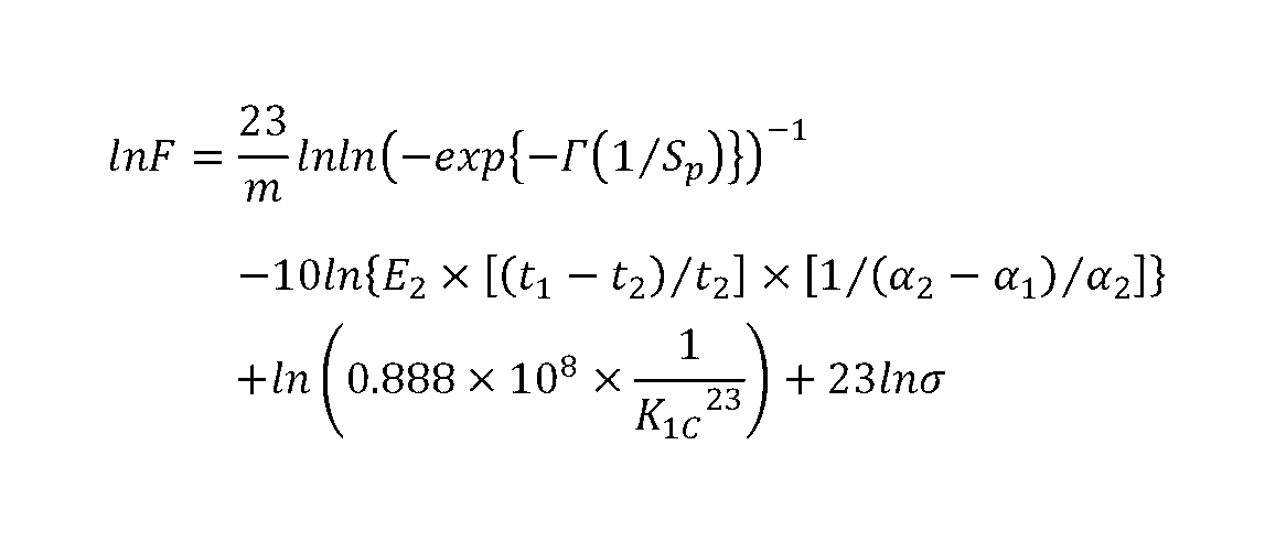
- the substrate holding member of the present disclosure is a substrate holding member provided with a main body made of a plate-like ceramic and a coating film that covers the surface of the main body, and the ceramic has a fracture toughness of K 1C , a thermal expansion coefficient Is ⁇ 1, thickness is t1, Young's modulus is E1, thermal expansion coefficient of the covering film is ⁇ 2, thickness is t2, Young's modulus is E2, compressive strength is ⁇ , and safety factor of the substrate holding member is Sp When t1 is 0.5 mm or more and 30 mm or less, t2 is 3 ⁇ m or more and 0.1 t1 or less, and the F value represented by Formula 1 is 1 ⁇ 10 22 or more. Further, a semiconductor manufacturing apparatus of the present disclosure includes the above-described substrate holding member.
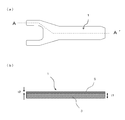
- FIG. 2 is a schematic view of a substrate holding member according to an embodiment of the present invention, in which (a) is a top view and (b) is a cross-sectional view taken along the line AA ′. It is the schematic which shows the model used for stress analysis. It is an example of the chemical structure of PI. It is a chemical structure of PBI.
- the substrate holding member is a member used for holding and transporting the substrate in the semiconductor manufacturing apparatus, and for example, a processing chamber, a holding pin for holding the substrate in the load lock chamber, and a carrier for transporting the substrate in the apparatus It is an arm etc.
- FIG. 1 is a schematic view of a substrate holding member 1 (transfer arm) according to an embodiment of the present invention.
- the substrate holding member 1 of the present disclosure includes a main body 3 made of ceramic and a covering film 5 that covers the surface of the main body 3.
- the thickness t1 of the main body 3 is in the range of 0.5 mm to 30 mm, the thickness t2 of the covering film 5 is 3 ⁇ m or more, and the range of 1/10 or less of the thickness t1 of the main body 3.
- the fracture toughness of the ceramic is K 1C
- the thermal expansion coefficient is ⁇ 1
- the thickness is t1
- the Young's modulus is E1
- the Weibull coefficient is m
- the thermal expansion coefficient of the covering film 5 is ⁇ 2
- the F value represented by Formula 1 is 1 ⁇ 10 22 or more.
- the compressive strength of the resin is the yield strength.
- Sp value (it is also called a safety factor) in Formula 1 is stress analysis software which used compressive strength ⁇ of resin which forms covering film 5 using a finite element method made by Siemens as shown in Formula 2. It is a value divided by ⁇ f calculated using NX (version 11.0.0.33). This ⁇ f is the maximum value when the generated stress is calculated using a model.
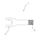
- the thicknesses of the main body 3 and the covering film 5 were changed using the model 2 of the shape shown in FIG. 2 to calculate ⁇ f. Further, the thermal expansion coefficients and Young's modulus values of the main body 3 and the covering film 5 were also changed.
- Model 2 of FIG. 2 is a transfer arm 2 for mounting a substrate on a substrate support 2a divided into two, and the end on the opposite side of the substrate support 2a attaches the transfer arm 2 to the substrate transfer apparatus It is the attachment part 2b.
- the covering film 5 covers the entire surface on one side of the main body 3. Then, in FIG. 2, when the covering film 5 of the substrate support portion 2a in the hatched range is 300 ° C., and the attachment portion 2b in the hatched range is 20 ° C., ⁇ f generated in the model 2 is NX Calculated.
- the compression strength of the resin forming the covering film 5 was divided by the ⁇ f calculated in this manner to calculate the Sp value. Then, the Sp value calculated using NX was substituted into equation 1, and the thicknesses of the main body 3 and the covering film 5, the thermal expansion coefficient, and the Young's modulus were also substituted. Further, fracture toughness was substituted for the main body 3 and strength was substituted for the covering film 5.
- This equation 1 is based on the life prediction generated from the natural defect contained in the member of the substrate holding member 1, and the variation of the natural defect inherent in the substrate holding member 1, the substrate holding member 1 and the coating The influence of parameters such as the thermal expansion coefficient difference of the film 5 on the durability of the substrate holding member 1 is quantified.
- Each value regarding the ceramics substituted to Formula 1 is measured by the method shown in Table 1. In the simulation to be described later, the values described in Table 1 were used for the respective values of the ceramics.
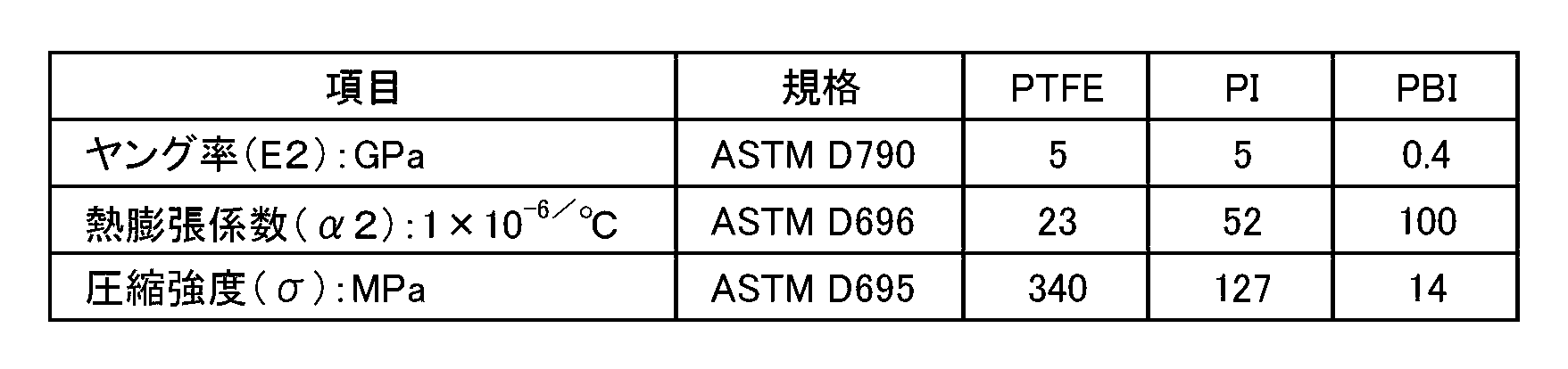
- each value regarding resin substituted to Formula 1 is measured by the method shown in Table 2.
- each value regarding resin which forms the coating film 5 used the value described in Table 2.
- the Young's modulus of the resin is a value calculated from the flexural modulus.
- each value is directly measured from the substrate holding member 1 It is not possible. In such a case, a test piece may be prepared and measured separately from the substrate holding member 1.
- data provided by a ceramic or resin supplier may be used.
- the values described in Tables 1 and 2 may be used.
- the value described in the second method of selecting the plastic material of the JIS usage series new edition issued by Japan Standards Association may be used.
- the resin can be specified, for example, using infrared spectroscopy (IR), nuclear magnetic resonance (NMR), thermal decomposition gas chromatography-mass spectrometry (Py-GC-MS) or the like.
- IR infrared spectroscopy
- NMR nuclear magnetic resonance
- Py-GC-MS thermal decomposition gas chromatography-mass spectrometry
- the substrate holding member 1 of the present disclosure that satisfies the equation 1 has excellent durability.
- the F-number satisfy 1 ⁇ 10 30 or more. It becomes the board
- the substrate holding member 1 is excellent in heat resistance and can be used at high temperatures.
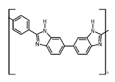
- the resin having a high glass transition temperature include polyimide (PI) and polybenzimidazole (PBI).
- FIG. 3 shows a typical PI chemical structure.
- PI is a generic term for polymers containing an imide bond in the repeating unit.
- Figure 4 shows the chemical structure of PBI.
- Benzimidazole is an organic compound represented by a molecular formula C 7 H 6 N 2 , and is a heterocyclic compound in which a benzene ring and an imidazole ring are bonded by sharing one side.
- the heat resistance temperature (glass transition temperature) of PBI is about 427 ° C.
- the heat resistance temperature of PI is about 285 ° C. to 410 ° C., which is higher than the heat resistance temperature (about 260 ° C.) of tetrafluoroethylene resin (PTFE).
- the heat resistant temperature of PI of the structure shown in FIG. 3 is 410.degree. Therefore, if PI is used as the resin, it can be used even when the temperature of the substrate exceeds 260 ° C.
- the tensile strength of PBI is about 160 MPa, and the tensile strength of PI is about 86 MPa, which is higher than the tensile strength of PTFE (about 20 to 35 MPa). Therefore, even if there is vibration or the like of the device, peeling of resin at the contact portion between the substrate holding member 1 and the substrate is unlikely to occur.
- a resin having conductivity may be used as the covering film 5.
- electrostatic breakdown of the substrate can be suppressed.
- resin which has electroconductivity what added the electroconductivity imparting agent of carbon, a metal, etc. to various resin is mentioned.
- metal powder or carbon powder may be added to the resin.
- Each value of the resin substituted into Formula 1 in that case may use each value of the main component of resin except metal powder and carbon powder. That is, when the resin is a matrix and the additive is dispersed in the matrix, the characteristics of the resin which is the matrix are dominant, so the influence on the calculation of the F value can be ignored.
- the surface resistivity of the coating film 5 be 10 4 ⁇ / sq or more and 10 10 ⁇ / sq or less. If the surface resistivity is in the above range, sparks are unlikely to occur and static electricity can be sufficiently removed. When the thickness of the coating film 5 is 10 ⁇ m or more, it becomes easy to coat the main body 3.
- the conductivity imparting additive (hereinafter also referred to as an additive) imparts conductivity to the resin by being added to the resin.
- the additive is an inorganic material such as carbon, metal, metal oxide, metal salt or the like, the conductivity can be easily adjusted as compared with the organic material, and deterioration and degassing are less even if the temperature rises.
- the additive itself is conductive, such as carbon and metal, the conductivity becomes high.
- metals to be added titanium, zinc, tin, alkali metals, alkaline earth metals, and alloys thereof are preferable.
- the amount of the metal additive to the total amount of the resin so that the surface resistivity of the coating film 5 is 10 4 ⁇ / ⁇ or more and 10 10 ⁇ / ⁇ or less, it has an elimination effect of static electricity. Can.
- the covering film 5 may cover the entire surface of the main body 3 but may be disposed at least at a part of the substrate support 2a. Furthermore, when the covering film 5 has conductivity, it is possible to suppress electrostatic breakdown of the substrate.
- alumina-based ceramics also described as Al 2 O 3
- silicon carbide-based ceramics also described as SiC
- cordierite-based ceramics also described as 2MgO ⁇ 2Al 2 O 3 ⁇ 5SiO 2 , CO
- silicon nitride Ceramics also described as Si 3 N 4
- alumina ceramics, silicon carbide ceramics, and cordierite ceramics may be used. The use of these ceramics results in the substrate holding member 1 having excellent durability.
- the ceramic may be conductive for the same reason as the coating film 5.
- the thickness of the main body is changed in the range of 0.5 to 30 mm, and the thickness of the covering film 5 is changed in the range of 0.003 mm (3 ⁇ m) to 3 mm
- Tables 3 to 11 show F values in the formula 1 of I omitted some of the combinations. Also, in the table, 1 ⁇ 10 22 is written as 1.0E + 22.
- one combination (frame) of t1 and t2 is expressed as one area in the table.
- the F value was 1 ⁇ 10 22 or more in the five regions in the table.
- the F value of 1 ⁇ 10 22 or more is indicated in bold in the table.
- a combination having an F value of 1 ⁇ 10 22 or more will have durability superior to that of a substrate holding member coated with ceramics, which has been conventionally used.
- PI When PI is used as a resin and considered in combination with four types of ceramics, when PI is used as a resin, a substrate having excellent durability by combining Al 2 O 3 , SiC, and CO as ceramics. It becomes the holding member 1.
- the F value As shown in Table 8, when PBI was used as the resin and Al 2 O 3 was used as the ceramic, the F value became 1 ⁇ 10 22 or more in the 17 region in the table. Further, as shown in Table 9, when PBI was used as the resin and SiC was used as the ceramic, the F value was 1 ⁇ 10 22 or more in all the regions in the table. In addition, as shown in Table 10, when PBI was used as the resin and Si 3 N 4 was used as the ceramic, the F value was 1 ⁇ 10 22 or more in the 15 region in the table. As shown in Table 11, when PI was used as the resin and cordierite was used as the ceramic, the F value was 1 ⁇ 10 22 or more in all of the amount ranges in the table.
- the width of the combination of the thickness of the main body 3 and the thickness of the resin 5 which can improve the durability of the substrate holding member 1 widens.
- the substrate holding member 1 of the present disclosure can be used as a transfer arm.
- PBI or PI which is excellent in heat resistance, is used as a resin
- handling can be performed without waiting for the temperature of the substrate heated by various processes to drop to normal temperature, and therefore the tact time can be shortened.
- a semiconductor manufacturing apparatus using the above substrate holding member 1 is excellent in durability.
- the semiconductor manufacturing apparatus is used in the manufacturing process of semiconductor elements and liquid crystal display devices.
- Examples of the semiconductor manufacturing apparatus include an exposure apparatus, a CVD apparatus, and a dry etching apparatus. In these apparatuses, after the substrate is carried into the processing unit of the apparatus, subjected to desired processing, and then taken out, the element and circuit are formed on the substrate by repeating the cycle.
- the substrate holding member 1 can have the function of removing static electricity by the coating film 5 being electrically connected to the ground.
- the covering film 5 does not have to cover the entire surface of the main body 3, and the thicknesses of the main body 3 and the covering film 5 may also be changed depending on the position.
- the thicknesses of the main body 3 and the covering film 5 of the portion of the substrate support 2a in contact with the substrate may be controlled within the range of the present disclosure.
- the thicknesses of the main body 3 and the covering film 5 are changed, the thicknesses of the main body 3 and the covering film 5 of the portion in contact with the substrate are used in the substrate support portion 2a Just do it.
- Substrate holding member 2 Model 2a: Substrate supporting portion 2b: Mounting portion 3: Main body 5: Coating film
Landscapes
- Engineering & Computer Science (AREA)
- Chemical & Material Sciences (AREA)
- Ceramic Engineering (AREA)
- Materials Engineering (AREA)
- Structural Engineering (AREA)
- Organic Chemistry (AREA)
- Robotics (AREA)
- Mechanical Engineering (AREA)
- Container, Conveyance, Adherence, Positioning, Of Wafer (AREA)
- Manipulator (AREA)
Abstract
本開示の基板保持部材は、板状のセラミックスからなる本体と、前記本体の表面を被覆する被覆膜とを備えた基板保持部材であって、前記セラミックスの破壊靱性をK1C、熱膨張係数をα1、厚みをt1、ヤング率をE1とし、前記被覆膜の熱膨張係数をα2、厚みをt2、ヤング率をE2、圧縮強度をσとし、前記基板保持部材の安全率をSpとしたとき、t1は、0.5mm以上、30mm以下であり、t2は、3μm以上、0.1t1以下であり、式1で表されるF値が、1×10²²以上である。また、本開示の半導体製造装置は、上記の基板保持部材を備える。
Description
本発明は、半導体製造装置などで、基板の保持に使用される基板保持部材に関する。
半導体素子や液晶表示装置の製造工程では、露光装置、CVD装置、ドライエッチング装置などの半導体製造装置を用いて、基板に素子や回路を形成する。これらの装置では、基板を装置の処理部に搬入し、所望の処理を施した後、搬出するというサイクルを繰り返す。処理の際、基板が加熱されることから、基板の温度を、基板に接触して保持、または搬送する部材(以下、基板保持部材という)の耐熱温度以下にして搬送する必要があり、基板保持部材の耐熱性がタクトタイムに影響する。特許文献1には、セラミックス部材をコートするための樹脂として、PTFE(ポリテトラフルオロエチレン)が記載されている。
本開示の基板保持部材は、板状のセラミックスからなる本体と、前記本体の表面を被覆する被覆膜とを備えた基板保持部材であって、前記セラミックスの破壊靱性をK1C、熱膨張係数をα1、厚みをt1、ヤング率をE1とし、前記被覆膜の熱膨張係数をα2、厚みをt2、ヤング率をE2、圧縮強度をσとし、前記基板保持部材の安全率をSpとしたとき、t1は、0.5mm以上、30mm以下であり、t2は、3μm以上、0.1t1以下であり、式1で表されるF値が、1×10²²以上である。また、本開示の半導体製造装置は、上記の基板保持部材を備えたものである。
以下、本発明の実施形態について説明する。
基板保持部材は、半導体製造装置で基板の保持、搬送に使用される部材であり、例えば、処理室、ロードロック室で基板を保持するための保持ピン、装置内で基板を搬送するための搬送アームなどである。図1に本発明の一実施形態である基板保持部材1(搬送アーム)の概略図を示す。
本開示の基板保持部材1は、セラミックスからなる本体3と、本体3の表面を被覆する被覆膜5とを備えている。そして、本体3の厚みt1は、0.5mm~30mmの範囲であり、被覆膜5の厚みt2は、3μm以上であり、本体3の厚みt1の1/10以下の範囲である。
本体3の厚みを0.5mm以上としたのは基板保持部材1の機械的な強度、剛性を維持できるからである。また、本体3の厚みt1を30mm以下としたのは、基板保持部材1の重量を比較的小さくすることができるからである。
被覆膜5の厚みt2を3μm以上としたのは、被覆膜5の破損を抑制することができるからである。また、被覆膜5の厚みt2を本体3の厚みt1の1/10以下としたのは、基板保持部材1の重量の増加を抑制できるからである。
また、本開示の基板保持部材1は、セラミックスの破壊靱性をK1C、熱膨張係数をα1、厚みをt1、ヤング率をE1、ワイブル係数をmとし、被覆膜5の熱膨張係数をα2、厚みをt2、ヤング率をE2、圧縮強度をσとしたとき、式1で表されるF値が、1×10²²以上となる。なお、樹脂の圧縮強度は、降伏強度である。
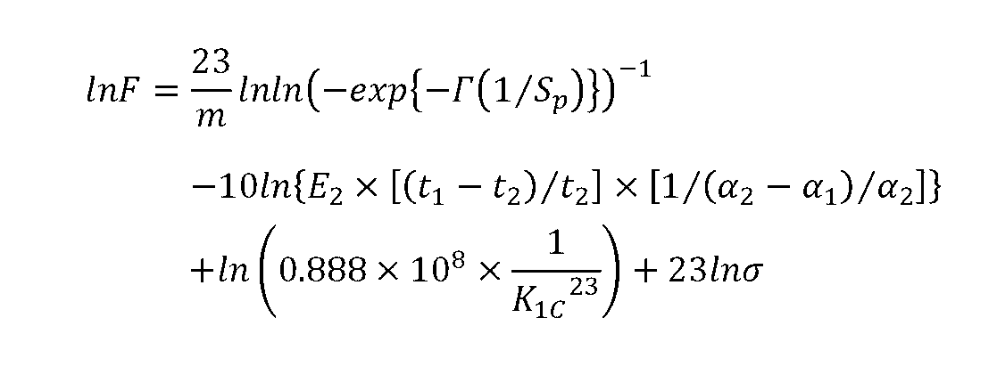
なお、式1中のSp値(安全率ともいう)は、式2に示すように、被覆膜5を形成する樹脂の圧縮強度σを、シーメンス社製の有限要素法を用いた応力解析ソフトであるNX(バージョン11.0.0.33)を用いて算出したσfで割った値である。このσfは、モデルを用いて、発生する応力を計算したときの最大値である。

図2に示す形状のモデル2を用いて、本体3と被覆膜5の厚みを変化させて、σfを算出した。また、本体3と被覆膜5の熱膨張係数、ヤング率の値もそれぞれ変化させた。
図2のモデル2は、2つに分かれた基板支持部2aの上に基板を載置する搬送アーム2であり、基板支持部2aと反対側の端部が搬送アーム2を基板搬送装置に取り付ける取り付け部2bである。
図2におけるモデル2では、被覆膜5は、本体3の片面の全面を覆っている。そして、図2において、斜線で示す範囲の基板支持部2aの被覆膜5が300℃であり、斜線で示す範囲の取り付け部2bを20℃としたとき、モデル2に発生するσfをNXで算出した。
NXの設定は、メッシュタイプとして3D四面体を選択し、メッシュパラメータの要素サイズは4mmとした。また、フリーマップドメッシュの試行を選択した。重力加速度は9.810mm/sec2とした。多角形ジオメトリの高解像度化、接点の接続は、使わなかった。
このようにして算出したσfで、被覆膜5を形成する樹脂の圧縮強度を割って、Sp値を算出した。そして、さらに、NXを用いて算出したSp値を式1に代入し、あわせて、本体3と被覆膜5の厚み、熱膨張係数、ヤング率の値も代入した。また、本体3については、破壊靱性を代入し、被覆膜5については、強度を代入した。
この式1から算出したF値が大きいほど、基板保持部材1の寿命が長くなることを意味する。
この式1は、基板保持部材1の部材中に含まれる自然欠陥から発生した寿命予測を基礎とするものであり、基板保持部材1に内在する自然欠陥のバラツキや、基板保持部材1と被覆膜5の熱膨張係数差等のパラメータが基板保持部材1の耐久性に与える影響を数値化したものである。
なお、式1の関係を充足するとき、基板保持部材1の構成要素のうち最初に樹脂からなる被覆膜5が壊れる。そこで、式を単純化するため、破壊しないセラミックスの強度は数1から除外した。また、同様の理由から、セラミックスのワイブル係数mは、セラミックスの種類によらず15として計算した。
式1に、代入するセラミックスに関する各値は、表1に示す方法で測定する。なお、後述するシミュレーションでは、セラミックスに関する各値は表1に記載した値を用いた。
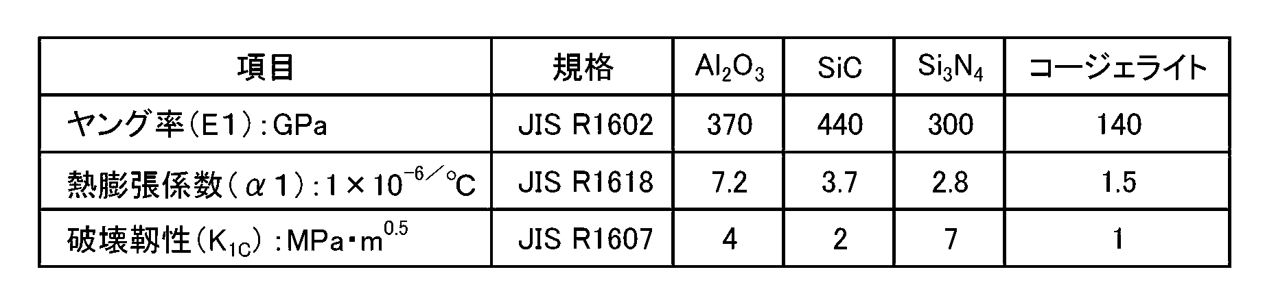
また、式1に代入する樹脂に関する各値は、表2に示す方法で測定する。なお、後述するシミュレーションでは、被覆膜5を形成する樹脂に関する各値は表2に記載した値を用いた。樹脂のヤング率は、曲げ弾性率から算出した値である。
なお、式1に代入する各値を求めるにあたり、表1、2に示す測定方法に定められている大きさなどの試験条件を満たさない場合には、各値を基板保持部材1から直接測定することはできない。その様な場合、基板保持部材1とは別に試験片を準備して測定してもよい。
また、セラミックスや樹脂の供給元から提供されたデータを用いてもよい。あるいは、例えば、表1、2に記載した値を用いてもよい。また、例えば、財団法人日本規格協会が発行するJIS使い方シリーズ新版プラスチック材料選択のポイント第2版に記載された値を用いてもよい。また、これらに記載されていない材料を用いる場合には、朝倉書店が出版しているプラスチック事典のデータを用いてもよい。
なお、セラミックスの特定は、例えば、XRDを用いて行うことができる。また、樹脂の特定は、例えば、赤外分光法(IR)、核磁気共鳴法(NMR)、熱分解ガスクロマトグラフ-質量分析法(Py-GC-MS)などを用いて行うことができる。
式1を充足する本開示の基板保持部材1は優れた耐久性を有している。
さらに、F値が1×1030以上を充足するとよい。このような構成であるとさらに優れた耐久性を有する基板保持部材1となる。
また、被覆膜5としてガラス転移温度が270℃以上の樹脂を用いると、耐熱性に優れ、高温での使用が可能な基板保持部材1となる。ガラス転移温度が高い樹脂として、例えば、ポリイミド(PI)やポリベンゾイミダゾール(PBI)が挙げられる。
図3に代表的なPIの化学構造を示す。PIは、繰り返し単位にイミド結合を含む高分子の総称である。
図4にPBIの化学構造を。ベンゾイミダゾールは分子式C7H6N2で表される有機化合物で、ベンゼン環とイミダゾール環が一辺を共有して結合した複素環式化合物である。
これらの樹脂は強度、耐熱性に優れるため、耐久性に優れた基板保持部材1となる。
PBIの耐熱温度(ガラス転移温度)は約427℃、PIの耐熱温度は約285℃~410℃であり、テトラフルオロエチレン樹脂(PTFE)の耐熱温度(約260℃)よりも高い。図3に示す構造のPIの耐熱温度は410℃である。そのため、樹脂としてPIを用いると、基板が260℃を越える温度となっても使用可能である。
PBIの引張強度は、約160MPa、PIの引張強度は約86MPaであり、PTFEの引張強度(約20~35MPa)よりも高い。そのため、装置の振動などがあっても、基板保持部材1と基板との接触部での樹脂はがれが起こりにくい。
また、被覆膜5として、導電性を有する樹脂を用いてもよい。このような樹脂を用いると、基板の静電破壊を抑制することができる。導電性を有する樹脂としては、種々の樹脂にカーボンや金属などの導電性付与剤を添加したものが挙げられる。
被覆膜5に導電性を付与する場合、例えば、金属粉末や炭素粉末を樹脂に添加すればよい。その場合の式1に代入する樹脂の各値は、金属粉末や炭素粉末を除く、樹脂の主成分の各値を用いればよい。つまり、樹脂がマトリックスで添加物がマトリックス中に分散している場合には、マトリックスである樹脂の特性が支配的となるため、F値の算出に与える影響は無視することができる。
被覆膜5の表面抵抗率が104Ω/□以上1010Ω/□以下であれば好適である。表面抵抗率が上記範囲であれば、スパークが生じにくく、かつ、静電気を充分に除去できる。被覆膜5の厚みを、10μm以上とすると、本体3を被覆することが容易となる。
導電性付与添加物(以下、添加物ともいう)は、樹脂に添加することで、樹脂に導電性を付与する。添加物が、炭素、金属、金属酸化物、金属塩などの無機材料であると、有機材料と比べて、導電率調整がし易く、温度が上がっても変質および脱ガスが少ない。特に添加物が、炭素、金属のように、添加物自体が導電性を有していると導電率が高くなる。添加する金属としては、チタン、亜鉛、錫、アルカリ金属、アルカリ土類金属、およびそれらの合金などが好適である。そして、被覆膜5の表面抵抗率が104Ω/□以上1010Ω/□以下となるように、樹脂の総量に対する金属添加物の量を調整することで、静電気の除去作用を有することができる。
被覆膜5は、本体3の表面全体を被覆していてもよいが、少なくとも、基板支持部2aの一部に配置されているとよい。さらに、基板支持部2aから取り付け部2bまで連続して配置されており、被覆膜5が導電性を有する場合には、基板の静電破壊を抑制することができる。
本体3を構成するセラミックスとして、種々の材質を用いることができる。例えば、アルミナ質セラミックス(Al2O3とも表記する)、炭化珪素質セラミックス(SiCとも表記する)、コージェライト質セラミックス(2MgO・2Al2O3・5SiO2、COとも表記する)、窒化珪素質セラミックス(Si3N4とも表記する)が挙げられる。特に、アルミナ質セラミックス、炭化珪素質セラミックス、コージェライト質セラミックスを用いてもよい。これらのセラミックスを用いると耐久性に優れた基板保持部材1となる。
また、セラミックスは、被覆膜5と同様の理由により、導電性を有するものとしてもよい。
以下に、数1を用いたシミュレーションについて、説明する。
セラミックスとして、Al2O3、SiC、Si3N4、CO、樹脂として、PTFE、PI、PBIを組み合わせ、表1、2に記載した、それぞれの特性に基づいて、有限要素法に基づく基板保持部材1の耐久性との関係を調査した。
表1のセラミックスと表2の樹脂とを組み合わせ、本体の厚みを0.5~30mmの範囲で変化させ、被覆膜5の厚みを0.003mm(3μm)から3mmの範囲で変化させた場合の式1におけるF値を表3~表11に示す。なお、一部の組み合わせについては割愛した。また、表中において、1×10²²は、1.0E+22と表記している。

表3に示すように、樹脂としてPTFEを用い、セラミックスとしてAl2O3を用いた場合、t1とt2の全ての組み合わせでF値は1×10²²未満となった。同様に、セラミックスとして、SiC、Si3N4、COを用い、樹脂としてPTFEを用いた場合、t1とt2の全ての組み合わせでF値は1×10²²未満となったため、Al2O3とPTFE以外の組み合わせについては、表を割愛した。
なお、以下では、表中でt1とt2の一つの組み合わせ(枠)を一つの領域と表現する。
次に、樹脂として、PIを用い、4種のセラミックスと組み合わせた場合のF値を表4~7に示す。
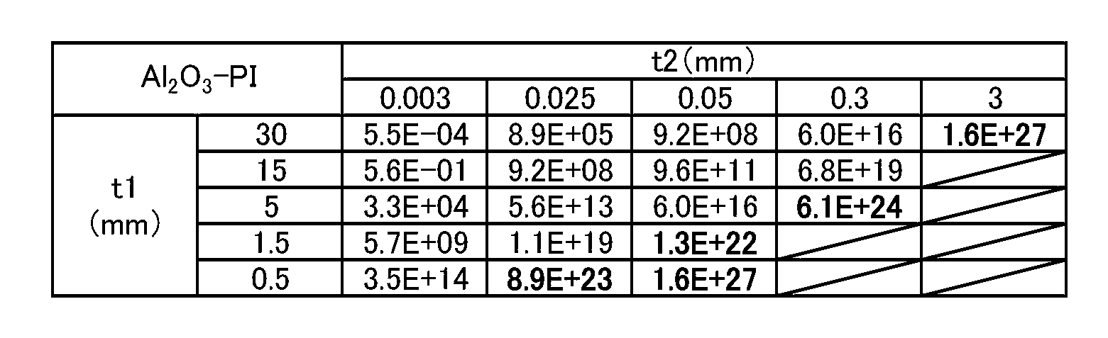

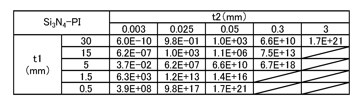

表4に示すように、樹脂としてPIを用い、セラミックスとしてAl2O3を用いた場合、表中の5つの領域でF値が1×10²²以上となった。なお、1×10²²以上のF値は、表中において太字で表記した。
また、表5に示すように、樹脂としてPIを用い、セラミックスとしてSiCを用いた場合、表中の10の領域でF値が1×10²²以上となった。また、表6に示すように、樹脂としてPIを用い、セラミックスとしてSi3N4を用いた場合は、F値が1×10²²以上の領域はなかった。表7に示すように樹脂としてPIを用い、セラミックスとしてCOを用いた場合は、表中の10の量域でF値が1×10²²以上となった。
F値が1×10²²以上の組み合わせは、従来、用いられていたPTFEでセラミックスを被覆した基板保持部材よりも優れた耐久性を有することになる。
樹脂としてPIを用い、4種のセラミックスと組み合わせた場合について検討すると、樹脂として、PIを用いた場合には、セラミックスとしてAl2O3、SiC、COを組み合わせることによって、耐久性の優れた基板保持部材1となる。
次に、樹脂として、PBIを用い、4種のセラミックスと組み合わせた場合のF値を表8~11に示す。


表8に示すように、樹脂としてPBIを用い、セラミックスとしてAl2O3を用いた場合、表中の17の領域でF値が1×10²²以上となった。また、表9に示すように、樹脂としてPBIを用い、セラミックスとしてSiCを用いた場合、表中の全ての領域でF値が1×10²²以上となった。また、表10に示すように、樹脂としてPBIを用い、セラミックスとしてSi3N4を用いた場合は、表中の15の領域でF値が1×10²²以上となった。表11に示すように樹脂としてPIを用い、セラミックスとしてコージェライトを用いた場合は、表中の全ての量域でF値が1×10²²以上となった。
樹脂としてPBIを用いると、PIを用いた場合よりも、F値が1×10²²以上の領域が増加した。
以上説明したとおり、樹脂としてPI、PBIを用いると、基板保持部材1の耐久性を向上させることができる本体3および樹脂5の厚みの組み合わせの幅が広がることがわかる。
本開示の基板保持部材1は、搬送アームとして用いることができる。樹脂として、耐熱性に優れるPBIやPIを用いると、種々の加工により加熱された基板の温度が常温に下がるまで待つことなく、取り扱うことができるためタクトタイムを短くすることができる。
上記の基板保持部材1を用いた半導体製造装置は、耐久性に優れたものとなる。
半導体製造装置は、半導体素子や液晶表示装置の製造工程で使用される。半導体製造装置として、例えば露光装置、CVD装置、ドライエッチング装置などがある。これらの装置では、基板を装置の処理部に搬入し、所望の処理を施した後、搬出するというサイクルを繰り返して、基板に素子や回路を形成する。半導体製造装置において、被覆膜5が、アースと電気的に接続されることで、基板保持部材1は静電気の除去作用を有することができる。
以上、本発明の実施形態について説明したが、本発明は上述の実施形態に限定されず、本発明の要旨を逸脱しない範囲において、各種の改良および変更を行なってもよい。例えば、被覆膜5は本体3の全面を覆う必要はなく、本体3および被覆膜5の厚みも位置によって変化させてもよい。例えば、基板支持部2aにおいて基板と接触する部分の本体3および被覆膜5の厚みを本開示の範囲に制御すればよい。本体3や被覆膜5の厚みが変化している形態では、数1、2を用いた計算では、基板支持部2aにおいて、基板と接触する部分の本体3および被覆膜5の厚みを用いればよい。
1 :基板保持部材
2 :モデル
2a:基板支持部
2b:取り付け部
3 :本体
5 :被覆膜
2 :モデル
2a:基板支持部
2b:取り付け部
3 :本体
5 :被覆膜
Claims (8)
- 板状のセラミックスからなる本体と、
前記本体の表面を被覆する被覆膜とを備えた基板保持部材であって、
前記セラミックスの破壊靱性をK1C、熱膨張係数をα1、厚みをt1、ヤング率をE1とし、
前記被覆膜の熱膨張係数をα2、厚みをt2、ヤング率をE2、圧縮強度をσとし、
前記基板保持部材の安全率をSpとしたとき、
t1は、0.5mm以上、30mm以下であり、
t2は、3μm以上、0.1t1以下であり、
式1で表されるF値が、1×10²²以上である、基板保持部材。
- 上記F値が、1×1030以上である、請求項1に記載の基板保持部材。
- 前記被覆膜は、ガラス転移温度が270℃以上である、請求項1または2に記載の基板保持部材。
- 前記被覆膜は、PBIまたはPIである、請求項1乃至3のいずれかに記載の基板保持部材。
- 前記被覆膜は、導電性を有する、請求項1乃至4のいずれかに記載の基板保持部材。
- 前記セラミックスは、アルミナ質セラミックス、炭化珪素質セラミックス、コージェライト質セラミックスから選ばれるいずれかである、請求項1乃至5のいずれかに記載の基板保持部材。
- 前記セラミックスは、導電性を有する、請求項1乃至6のいずれかに記載の基板保持部材。
- 請求項1~7に記載の基板保持部材を備えた半導体製造装置。
Priority Applications (3)
| Application Number | Priority Date | Filing Date | Title |
|---|---|---|---|
| JP2019532896A JP6859008B2 (ja) | 2017-07-28 | 2018-07-30 | 基板保持部材および半導体製造装置 |
| CN201880047790.5A CN110945640B (zh) | 2017-07-28 | 2018-07-30 | 基板保持构件和半导体制造装置 |
| US16/633,090 US20200161167A1 (en) | 2017-07-28 | 2018-07-30 | Substrate holding member and semiconductor manufacturing device |
Applications Claiming Priority (2)
| Application Number | Priority Date | Filing Date | Title |
|---|---|---|---|
| JP2017146661 | 2017-07-28 | ||
| JP2017-146661 | 2017-07-28 |
Publications (1)
| Publication Number | Publication Date |
|---|---|
| WO2019022258A1 true WO2019022258A1 (ja) | 2019-01-31 |
Family
ID=65041029
Family Applications (1)
| Application Number | Title | Priority Date | Filing Date |
|---|---|---|---|
| PCT/JP2018/028483 Ceased WO2019022258A1 (ja) | 2017-07-28 | 2018-07-30 | 基板保持部材および半導体製造装置 |
Country Status (4)
| Country | Link |
|---|---|
| US (1) | US20200161167A1 (ja) |
| JP (1) | JP6859008B2 (ja) |
| CN (1) | CN110945640B (ja) |
| WO (1) | WO2019022258A1 (ja) |
Cited By (1)
| Publication number | Priority date | Publication date | Assignee | Title |
|---|---|---|---|---|
| JP2021118323A (ja) * | 2020-01-29 | 2021-08-10 | Hoya株式会社 | 静電チャッククリーナー及び静電チャックのクリーニング方法 |
Families Citing this family (1)
| Publication number | Priority date | Publication date | Assignee | Title |
|---|---|---|---|---|
| WO2022138662A1 (ja) * | 2020-12-23 | 2022-06-30 | 京セラ株式会社 | クランプ用治具、クランプ用治具の製造方法および洗浄装置 |
Citations (2)
| Publication number | Priority date | Publication date | Assignee | Title |
|---|---|---|---|---|
| JP2003285382A (ja) * | 2002-03-28 | 2003-10-07 | Dainippon Screen Mfg Co Ltd | 複合構造部材および該部材の製造方法 |
| JP2004134747A (ja) * | 2002-07-22 | 2004-04-30 | Applied Materials Inc | 高温基板移送用ロボット |
Family Cites Families (10)
| Publication number | Priority date | Publication date | Assignee | Title |
|---|---|---|---|---|
| JP4090771B2 (ja) * | 2002-03-28 | 2008-05-28 | 京セラ株式会社 | 半導電性セラミックス、並びにこれを用いた磁気ディスク基板用保持部材及び治工具 |
| CN100579333C (zh) * | 2003-01-23 | 2010-01-06 | 东丽株式会社 | 电路基板用部件、电路基板的制造方法及电路基板的制造装置 |
| JP4360847B2 (ja) * | 2003-06-30 | 2009-11-11 | 日本特殊陶業株式会社 | セラミック回路基板、放熱モジュール、および半導体装置 |
| KR20060030370A (ko) * | 2004-10-05 | 2006-04-10 | 주식회사 엘지화학 | 생체활성 세라믹 코팅 복합체의 제조방법 |
| JP2007311737A (ja) * | 2006-04-21 | 2007-11-29 | Hitachi Chem Co Ltd | 静電チャック |
| JP2008147309A (ja) * | 2006-12-07 | 2008-06-26 | Hitachi Metals Ltd | セラミックス基板およびこれを用いた半導体モジュール |
| CN101647109B (zh) * | 2007-03-29 | 2011-11-09 | 日本电气株式会社 | 半导体装置 |
| JP2010114434A (ja) * | 2008-10-08 | 2010-05-20 | Ngk Spark Plug Co Ltd | 部品内蔵配線基板及びその製造方法 |
| JP5744045B2 (ja) * | 2010-10-26 | 2015-07-01 | 京セラ株式会社 | コージェライト質セラミックスおよびこれを用いた半導体製造装置用部材 |
| WO2016042957A1 (ja) * | 2014-09-16 | 2016-03-24 | 日本碍子株式会社 | セラミック構造体、基板保持装置用部材及びセラミック構造体の製法 |
-
2018
- 2018-07-30 JP JP2019532896A patent/JP6859008B2/ja active Active
- 2018-07-30 CN CN201880047790.5A patent/CN110945640B/zh active Active
- 2018-07-30 US US16/633,090 patent/US20200161167A1/en not_active Abandoned
- 2018-07-30 WO PCT/JP2018/028483 patent/WO2019022258A1/ja not_active Ceased
Patent Citations (2)
| Publication number | Priority date | Publication date | Assignee | Title |
|---|---|---|---|---|
| JP2003285382A (ja) * | 2002-03-28 | 2003-10-07 | Dainippon Screen Mfg Co Ltd | 複合構造部材および該部材の製造方法 |
| JP2004134747A (ja) * | 2002-07-22 | 2004-04-30 | Applied Materials Inc | 高温基板移送用ロボット |
Cited By (1)
| Publication number | Priority date | Publication date | Assignee | Title |
|---|---|---|---|---|
| JP2021118323A (ja) * | 2020-01-29 | 2021-08-10 | Hoya株式会社 | 静電チャッククリーナー及び静電チャックのクリーニング方法 |
Also Published As
| Publication number | Publication date |
|---|---|
| JPWO2019022258A1 (ja) | 2020-07-16 |
| JP6859008B2 (ja) | 2021-04-14 |
| CN110945640A (zh) | 2020-03-31 |
| CN110945640B (zh) | 2023-10-31 |
| US20200161167A1 (en) | 2020-05-21 |
Similar Documents
| Publication | Publication Date | Title |
|---|---|---|
| US5665260A (en) | Ceramic electrostatic chuck with built-in heater | |
| TWI659828B (zh) | 附散熱用金屬材之結構物、印刷電路板、電子機器及散熱用金屬材 | |
| TWI532420B (zh) | 多層配線基板及使用該多層配線基板之探針卡 | |
| JP2001244320A (ja) | セラミック基板およびその製造方法 | |
| KR20050067085A (ko) | 정전 척과 그 제조 방법 및 알루미나 소결 부재와 그 제조방법 | |
| WO2019022258A1 (ja) | 基板保持部材および半導体製造装置 | |
| JP2005235672A (ja) | ヒータユニット及びそれを搭載した装置 | |
| CN117321755A (zh) | 散热电路基板、散热构件及散热电路基板的制造方法 | |
| CN112840741B (zh) | 陶瓷加热器 | |
| CN113039863B (zh) | 静电卡盘加热器 | |
| KR20080059501A (ko) | 정전 척이 부착된 세라믹 히터 | |
| JP2012096931A (ja) | 窒化アルミニウムを被覆した耐蝕性部材およびその製造方法 | |
| KR20180016702A (ko) | 후막형 압력센서 및 그 제조방법 | |
| JP3297571B2 (ja) | 静電チャック | |
| JP2020021922A (ja) | 基板加熱ユニットおよび表面板 | |
| CN113767467A (zh) | 电子部件模块及氮化硅电路基板 | |
| JP4338994B2 (ja) | 高剛性低熱膨張セラミックス部材 | |
| US20190276722A1 (en) | Composite material and method of forming same, and electrical component including composite material | |
| JP2010189257A (ja) | 結晶粒の方位を制御する結晶化法 | |
| JP7754779B2 (ja) | 保持装置 | |
| JP3869160B2 (ja) | 複層セラミックスヒータおよびその製造方法 | |
| US4936010A (en) | Method of forming dielectric layer on a metal substrate having improved adhesion | |
| JP2015070101A (ja) | 多層基板及びその製造方法 | |
| JP2002190372A (ja) | ホットプレートユニット | |
| Fukuda et al. | Effect of repeated thermal cycles on thermal stress in copper paste films on alumina substrates |
Legal Events
| Date | Code | Title | Description |
|---|---|---|---|
| 121 | Ep: the epo has been informed by wipo that ep was designated in this application |
Ref document number: 18838313 Country of ref document: EP Kind code of ref document: A1 |
|
| ENP | Entry into the national phase |
Ref document number: 2019532896 Country of ref document: JP Kind code of ref document: A |
|
| NENP | Non-entry into the national phase |
Ref country code: DE |
|
| 122 | Ep: pct application non-entry in european phase |
Ref document number: 18838313 Country of ref document: EP Kind code of ref document: A1 |