WO2019006905A1 - 一种显示面板及其制作方法 - Google Patents
一种显示面板及其制作方法 Download PDFInfo
- Publication number
- WO2019006905A1 WO2019006905A1 PCT/CN2017/106306 CN2017106306W WO2019006905A1 WO 2019006905 A1 WO2019006905 A1 WO 2019006905A1 CN 2017106306 W CN2017106306 W CN 2017106306W WO 2019006905 A1 WO2019006905 A1 WO 2019006905A1
- Authority
- WO
- WIPO (PCT)
- Prior art keywords
- substrate
- region
- spacer layer
- disposed
- driving
- Prior art date
- Legal status (The legal status is an assumption and is not a legal conclusion. Google has not performed a legal analysis and makes no representation as to the accuracy of the status listed.)
- Ceased
Links
Images


Classifications
-
- G—PHYSICS
- G02—OPTICS
- G02F—OPTICAL DEVICES OR ARRANGEMENTS FOR THE CONTROL OF LIGHT BY MODIFICATION OF THE OPTICAL PROPERTIES OF THE MEDIA OF THE ELEMENTS INVOLVED THEREIN; NON-LINEAR OPTICS; FREQUENCY-CHANGING OF LIGHT; OPTICAL LOGIC ELEMENTS; OPTICAL ANALOGUE/DIGITAL CONVERTERS
- G02F1/00—Devices or arrangements for the control of the intensity, colour, phase, polarisation or direction of light arriving from an independent light source, e.g. switching, gating or modulating; Non-linear optics
- G02F1/01—Devices or arrangements for the control of the intensity, colour, phase, polarisation or direction of light arriving from an independent light source, e.g. switching, gating or modulating; Non-linear optics for the control of the intensity, phase, polarisation or colour
- G02F1/13—Devices or arrangements for the control of the intensity, colour, phase, polarisation or direction of light arriving from an independent light source, e.g. switching, gating or modulating; Non-linear optics for the control of the intensity, phase, polarisation or colour based on liquid crystals, e.g. single liquid crystal display cells
- G02F1/133—Constructional arrangements; Operation of liquid crystal cells; Circuit arrangements
- G02F1/1333—Constructional arrangements; Manufacturing methods
- G02F1/1339—Gaskets; Spacers; Sealing of cells
- G02F1/13394—Gaskets; Spacers; Sealing of cells spacers regularly patterned on the cell subtrate, e.g. walls, pillars
-
- G—PHYSICS
- G02—OPTICS
- G02F—OPTICAL DEVICES OR ARRANGEMENTS FOR THE CONTROL OF LIGHT BY MODIFICATION OF THE OPTICAL PROPERTIES OF THE MEDIA OF THE ELEMENTS INVOLVED THEREIN; NON-LINEAR OPTICS; FREQUENCY-CHANGING OF LIGHT; OPTICAL LOGIC ELEMENTS; OPTICAL ANALOGUE/DIGITAL CONVERTERS
- G02F1/00—Devices or arrangements for the control of the intensity, colour, phase, polarisation or direction of light arriving from an independent light source, e.g. switching, gating or modulating; Non-linear optics
- G02F1/01—Devices or arrangements for the control of the intensity, colour, phase, polarisation or direction of light arriving from an independent light source, e.g. switching, gating or modulating; Non-linear optics for the control of the intensity, phase, polarisation or colour
- G02F1/13—Devices or arrangements for the control of the intensity, colour, phase, polarisation or direction of light arriving from an independent light source, e.g. switching, gating or modulating; Non-linear optics for the control of the intensity, phase, polarisation or colour based on liquid crystals, e.g. single liquid crystal display cells
- G02F1/133—Constructional arrangements; Operation of liquid crystal cells; Circuit arrangements
- G02F1/13306—Circuit arrangements or driving methods for the control of single liquid crystal cells
-
- G—PHYSICS
- G02—OPTICS
- G02F—OPTICAL DEVICES OR ARRANGEMENTS FOR THE CONTROL OF LIGHT BY MODIFICATION OF THE OPTICAL PROPERTIES OF THE MEDIA OF THE ELEMENTS INVOLVED THEREIN; NON-LINEAR OPTICS; FREQUENCY-CHANGING OF LIGHT; OPTICAL LOGIC ELEMENTS; OPTICAL ANALOGUE/DIGITAL CONVERTERS
- G02F1/00—Devices or arrangements for the control of the intensity, colour, phase, polarisation or direction of light arriving from an independent light source, e.g. switching, gating or modulating; Non-linear optics
- G02F1/01—Devices or arrangements for the control of the intensity, colour, phase, polarisation or direction of light arriving from an independent light source, e.g. switching, gating or modulating; Non-linear optics for the control of the intensity, phase, polarisation or colour
- G02F1/13—Devices or arrangements for the control of the intensity, colour, phase, polarisation or direction of light arriving from an independent light source, e.g. switching, gating or modulating; Non-linear optics for the control of the intensity, phase, polarisation or colour based on liquid crystals, e.g. single liquid crystal display cells
- G02F1/133—Constructional arrangements; Operation of liquid crystal cells; Circuit arrangements
- G02F1/1333—Constructional arrangements; Manufacturing methods
- G02F1/1345—Conductors connecting electrodes to cell terminals
- G02F1/13452—Conductors connecting driver circuitry and terminals of panels
-
- G—PHYSICS
- G02—OPTICS
- G02F—OPTICAL DEVICES OR ARRANGEMENTS FOR THE CONTROL OF LIGHT BY MODIFICATION OF THE OPTICAL PROPERTIES OF THE MEDIA OF THE ELEMENTS INVOLVED THEREIN; NON-LINEAR OPTICS; FREQUENCY-CHANGING OF LIGHT; OPTICAL LOGIC ELEMENTS; OPTICAL ANALOGUE/DIGITAL CONVERTERS
- G02F1/00—Devices or arrangements for the control of the intensity, colour, phase, polarisation or direction of light arriving from an independent light source, e.g. switching, gating or modulating; Non-linear optics
- G02F1/01—Devices or arrangements for the control of the intensity, colour, phase, polarisation or direction of light arriving from an independent light source, e.g. switching, gating or modulating; Non-linear optics for the control of the intensity, phase, polarisation or colour
- G02F1/13—Devices or arrangements for the control of the intensity, colour, phase, polarisation or direction of light arriving from an independent light source, e.g. switching, gating or modulating; Non-linear optics for the control of the intensity, phase, polarisation or colour based on liquid crystals, e.g. single liquid crystal display cells
- G02F1/133—Constructional arrangements; Operation of liquid crystal cells; Circuit arrangements
- G02F1/1333—Constructional arrangements; Manufacturing methods
- G02F1/1345—Conductors connecting electrodes to cell terminals
- G02F1/13454—Drivers integrated on the active matrix substrate
-
- G—PHYSICS
- G02—OPTICS
- G02F—OPTICAL DEVICES OR ARRANGEMENTS FOR THE CONTROL OF LIGHT BY MODIFICATION OF THE OPTICAL PROPERTIES OF THE MEDIA OF THE ELEMENTS INVOLVED THEREIN; NON-LINEAR OPTICS; FREQUENCY-CHANGING OF LIGHT; OPTICAL LOGIC ELEMENTS; OPTICAL ANALOGUE/DIGITAL CONVERTERS
- G02F1/00—Devices or arrangements for the control of the intensity, colour, phase, polarisation or direction of light arriving from an independent light source, e.g. switching, gating or modulating; Non-linear optics
- G02F1/01—Devices or arrangements for the control of the intensity, colour, phase, polarisation or direction of light arriving from an independent light source, e.g. switching, gating or modulating; Non-linear optics for the control of the intensity, phase, polarisation or colour
- G02F1/13—Devices or arrangements for the control of the intensity, colour, phase, polarisation or direction of light arriving from an independent light source, e.g. switching, gating or modulating; Non-linear optics for the control of the intensity, phase, polarisation or colour based on liquid crystals, e.g. single liquid crystal display cells
- G02F1/133—Constructional arrangements; Operation of liquid crystal cells; Circuit arrangements
- G02F1/136—Liquid crystal cells structurally associated with a semi-conducting layer or substrate, e.g. cells forming part of an integrated circuit
- G02F1/1362—Active matrix addressed cells
- G02F1/136286—Wiring, e.g. gate line, drain line
-
- G—PHYSICS
- G09—EDUCATION; CRYPTOGRAPHY; DISPLAY; ADVERTISING; SEALS
- G09G—ARRANGEMENTS OR CIRCUITS FOR CONTROL OF INDICATING DEVICES USING STATIC MEANS TO PRESENT VARIABLE INFORMATION
- G09G3/00—Control arrangements or circuits, of interest only in connection with visual indicators other than cathode-ray tubes
- G09G3/20—Control arrangements or circuits, of interest only in connection with visual indicators other than cathode-ray tubes for presentation of an assembly of a number of characters, e.g. a page, by composing the assembly by combination of individual elements arranged in a matrix no fixed position being assigned to or needed to be assigned to the individual characters or partial characters
- G09G3/34—Control arrangements or circuits, of interest only in connection with visual indicators other than cathode-ray tubes for presentation of an assembly of a number of characters, e.g. a page, by composing the assembly by combination of individual elements arranged in a matrix no fixed position being assigned to or needed to be assigned to the individual characters or partial characters by control of light from an independent source
- G09G3/36—Control arrangements or circuits, of interest only in connection with visual indicators other than cathode-ray tubes for presentation of an assembly of a number of characters, e.g. a page, by composing the assembly by combination of individual elements arranged in a matrix no fixed position being assigned to or needed to be assigned to the individual characters or partial characters by control of light from an independent source using liquid crystals
-
- G—PHYSICS
- G02—OPTICS
- G02F—OPTICAL DEVICES OR ARRANGEMENTS FOR THE CONTROL OF LIGHT BY MODIFICATION OF THE OPTICAL PROPERTIES OF THE MEDIA OF THE ELEMENTS INVOLVED THEREIN; NON-LINEAR OPTICS; FREQUENCY-CHANGING OF LIGHT; OPTICAL LOGIC ELEMENTS; OPTICAL ANALOGUE/DIGITAL CONVERTERS
- G02F1/00—Devices or arrangements for the control of the intensity, colour, phase, polarisation or direction of light arriving from an independent light source, e.g. switching, gating or modulating; Non-linear optics
- G02F1/01—Devices or arrangements for the control of the intensity, colour, phase, polarisation or direction of light arriving from an independent light source, e.g. switching, gating or modulating; Non-linear optics for the control of the intensity, phase, polarisation or colour
- G02F1/13—Devices or arrangements for the control of the intensity, colour, phase, polarisation or direction of light arriving from an independent light source, e.g. switching, gating or modulating; Non-linear optics for the control of the intensity, phase, polarisation or colour based on liquid crystals, e.g. single liquid crystal display cells
- G02F1/133—Constructional arrangements; Operation of liquid crystal cells; Circuit arrangements
- G02F1/1333—Constructional arrangements; Manufacturing methods
- G02F1/1339—Gaskets; Spacers; Sealing of cells
- G02F1/13398—Spacer materials; Spacer properties
-
- G—PHYSICS
- G02—OPTICS
- G02F—OPTICAL DEVICES OR ARRANGEMENTS FOR THE CONTROL OF LIGHT BY MODIFICATION OF THE OPTICAL PROPERTIES OF THE MEDIA OF THE ELEMENTS INVOLVED THEREIN; NON-LINEAR OPTICS; FREQUENCY-CHANGING OF LIGHT; OPTICAL LOGIC ELEMENTS; OPTICAL ANALOGUE/DIGITAL CONVERTERS
- G02F1/00—Devices or arrangements for the control of the intensity, colour, phase, polarisation or direction of light arriving from an independent light source, e.g. switching, gating or modulating; Non-linear optics
- G02F1/01—Devices or arrangements for the control of the intensity, colour, phase, polarisation or direction of light arriving from an independent light source, e.g. switching, gating or modulating; Non-linear optics for the control of the intensity, phase, polarisation or colour
- G02F1/13—Devices or arrangements for the control of the intensity, colour, phase, polarisation or direction of light arriving from an independent light source, e.g. switching, gating or modulating; Non-linear optics for the control of the intensity, phase, polarisation or colour based on liquid crystals, e.g. single liquid crystal display cells
- G02F1/133—Constructional arrangements; Operation of liquid crystal cells; Circuit arrangements
- G02F1/136—Liquid crystal cells structurally associated with a semi-conducting layer or substrate, e.g. cells forming part of an integrated circuit
- G02F1/13606—Liquid crystal cells structurally associated with a semi-conducting layer or substrate, e.g. cells forming part of an integrated circuit having means for reducing parasitic capacitance
-
- G—PHYSICS
- G02—OPTICS
- G02F—OPTICAL DEVICES OR ARRANGEMENTS FOR THE CONTROL OF LIGHT BY MODIFICATION OF THE OPTICAL PROPERTIES OF THE MEDIA OF THE ELEMENTS INVOLVED THEREIN; NON-LINEAR OPTICS; FREQUENCY-CHANGING OF LIGHT; OPTICAL LOGIC ELEMENTS; OPTICAL ANALOGUE/DIGITAL CONVERTERS
- G02F2202/00—Materials and properties
- G02F2202/02—Materials and properties organic material
- G02F2202/022—Materials and properties organic material polymeric
Definitions
- the present application relates to the field of display panel technologies, and in particular, to a display panel for reducing a resistance load of a circuit and a manufacturing method thereof.
- liquid crystal displays have become the mainstream products of displays due to their thin body, low power consumption and low radiation, and have been widely used.
- Most of the liquid crystal displays on the market are backlight type liquid crystal displays, which include a liquid crystal panel and a backlight module.
- the working principle of the liquid crystal panel is to place liquid crystal molecules in two parallel glass substrates, and apply a driving voltage on the two glass substrates to control the rotation direction of the liquid crystal molecules to refract the light of the backlight module to generate a picture.
- the thin film transistor liquid crystal display includes a liquid crystal panel and a backlight module, and the liquid crystal panel includes a second substrate (Color Filter Substrate, CF Substrate, also referred to as a color filter substrate), and a thin film transistor first substrate (Thin Film Transistor Substrate, TFT Substrate) And a mask, a transparent electrode is present on the opposite inner side of the substrate. A layer of liquid crystal molecules (LC) is sandwiched between the two substrates.
- LC liquid crystal molecules
- TFT-LCD Thin Film Transistor-Liquid Crystal Display
- GOA Gate Driver on Array circuits
- the GOA circuit is formed simultaneously with the in-plane structure of the first substrate by the same film formation method as the semiconductor device such as the in-plane liquid crystal drive switch, and its appearance eliminates the cost of the scan line driver chip, and at the same time There is no need to solder the flexible circuit board FPC to the edge of the liquid crystal display panel.
- the GOA circuit not only makes the control and design of the liquid crystal display more convenient, but also greatly reduces the width of the border of the liquid crystal display.
- GOA technology also has some problems that cannot be solved very well temporarily.
- the related circuit has a problem that the load capacity is too large.
- the technical problem to be solved by the present application is to provide a display panel capable of slowing down and reducing a resistance load of a circuit and a manufacturing method thereof
- the present application provides a display panel for reducing a resistance load of a circuit, and a manufacturing method thereof, the display panel comprising:
- a second substrate including a color resist layer, disposed opposite to the first substrate
- liquid crystal layer disposed between the first substrate and the second substrate
- the first substrate comprises a circuit area, and a display area
- the circuit area includes:
- a driver region integrated with a gate driver chip
- the spacer layer is respectively disposed between the first substrate and the second substrate corresponding to the driving region and the lead region;
- the spacer layer comprises a polystyrene material.
- the application also discloses a method for manufacturing a display panel, comprising the steps of:
- a spacer layer is disposed corresponding to the circuit region, and the spacer layer has a dielectric constant lower than that of the liquid crystal layer.
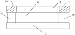
- FIG. 1 is a schematic view of a display panel of the present application
- FIG. 2 is a schematic view of a display panel according to an embodiment of the present application.
- FIG. 3 is a schematic view of a display panel according to another embodiment of the present application.
- Figure 4 is a diagram showing the arrangement structure corresponding to the embodiment shown in Figure 2;
- Figure 5 is a corresponding structural view of the embodiment shown in Figure 3;
- FIG. 6 is a flow chart of a method for fabricating a display panel of the present application.
- FIG. 1 is a schematic diagram of a display panel for reducing a resistance load of a circuit according to the present application, the display panel includes:
- the second substrate 20 includes a color resist layer (not shown) disposed opposite to the first substrate 10;
- liquid crystal layer 30 disposed between the first substrate 10 and the second substrate 20;
- the first substrate 10 includes a circuit area 11, and a display area 12 corresponding to the liquid crystal layer 30;
- a spacer layer 40 is formed on the circuit region, and the dielectric constant of the spacer layer 40 is lower than the dielectric constant of the liquid crystal layer 30.
- the circuit region 11 is a GOA circuit region; the spacer layer 40 is filled with a low dielectric material.
- a portion corresponding to the circuit region is provided with a dielectric
- FIG. 2 is a schematic view of an embodiment of the present application
- FIG. 3 is a schematic view of another embodiment of the present application
- FIG. 4 is a configuration diagram corresponding to the embodiment shown in FIG. 2
- FIG. 5 is a corresponding structure of the embodiment shown in FIG. Figure 2, Figure 5, together with Figure 1 shows:
- the circuit area 11 includes:
- a driving region 121 integrated with a gate driving chip
- the lead region 122 transmits a signal of the driving region 121 to the scan line in the display region 12;
- the spacer layer 40 is disposed between the first substrate 10 and the second substrate 20 corresponding to the driving region. Specifically, the cross-sectional shape of the spacer layer corresponds to the shape of the driving region.
- the capacitor of the circuit region includes a starting capacitor (Cd_com), and the starting capacitor (Cd_com) is mainly present in the driving region.
- a portion of the corresponding driving region is provided with a dielectric between the first substrate and the second substrate.
- the constant is lower than the spacer layer of the liquid crystal layer.
- the circuit area 11 includes:
- a driving region 121 integrated with a gate driving chip
- the lead region 122 transmits a signal of the driving region 121 to the scan line in the display region 12;
- the spacer layer 40 is disposed between the first substrate 10 and the second substrate 20 corresponding to the lead region 122.
- the cross-sectional shape of the spacer layer corresponds to the shape of the lead region.
- the capacitance of the circuit region includes a gate-drain capacitance (Cgd), and the gate-drain capacitance (Cgd) is mainly present in the lead region.
- Cgd gate-drain capacitance
- Cgd gate-drain capacitance
- Cgd gate-drain capacitance
- the circuit area 11 includes:
- a driving region 121 integrated with a gate driving chip
- the lead region 122 transmits a signal of the driving region 121 to the scan line in the display region 12;
- the spacer layer 40 is disposed between the first substrate 10 and the second substrate 20 corresponding to the driving region 121 and the lead region 122, respectively.
- the cross-sectional shape of the spacer layer corresponds to the overall shape of the driving region and the lead region.
- the capacitance of the circuit region includes a starting capacitor (Cd_com) and a gate drain capacitor (Cgd), and the starting capacitor (Cd_com) is mainly present in the driving region, and the gate-drain capacitance (Cgd) is mainly present in the lead region.
- the width of the spacer layer, etc. it is possible to match the size and shape of the corresponding driving area, lead area or circuit area as much as possible. Of course, it can be slightly larger or smaller, as long as it is compatible with the structure of the product. .
- a spacer supporting unit (not shown) is disposed between the first substrate 10 and the second substrate 20, and the spacer layer 40 and the spacer supporting unit are made of the same material.
- the spacer layer 40 includes a polystyrene material (PS material, that is, a Polystyrene material, which can be applied to a liquid crystal panel, which can be used as a material for manufacturing a spacer supporting unit, which is a PS/photo spacer).
- PS material polystyrene material
- the polystyrene material has a dielectric constant lower than 3 and lower than the dielectric constant of the liquid crystal layer, and is used as a corresponding filler in the circuit region, which can effectively reduce the overall dielectric constant of the polystyrene material.
- the spacer layer has a variety of materials to choose from, such as a low dielectric constant material based on silicon-based polymer or carbon doped silicon oxide, can also pass This is achieved by reducing the polarity of the material itself and increasing the density of the voids in the material, thereby reducing the molecular density of the material.
- the polystyrene material not only has its dielectric constant in accordance with the present case The demand, and the technology is mature, can be quickly utilized, and the cost is relatively low; in addition, the polystyrene material is used here, not only can effectively alleviate the problem of excessive resistance load, but also can be used as the first substrate.
- FIG. 6 is a diagram of a method for fabricating a display panel provided by the present application, the method comprising the steps of:
- a spacer layer is disposed corresponding to the circuit region, and the spacer layer has a dielectric constant lower than that of the liquid crystal layer.
- the step of forming the circuit region includes forming a driving region integrated with the function of the gate driving chip, and transmitting a signal of the driving region to the lead region of the scanning line in the display region;
- the spacer layer is disposed between the first substrate and the second substrate corresponding to the driving region. Specifically, the spacer layer is disposed corresponding to the driving region, and a cross-sectional shape of the spacer layer matches a shape of the driving region.
- the capacitor of the circuit region includes a starting capacitor (Cd_com), and the starting capacitor (Cd_com) is mainly present in the driving region.
- a portion of the corresponding driving region is provided with a dielectric between the first substrate and the second substrate.
- the dielectric constant of the spacer layer is lower than that of the liquid crystal. It can be seen that, after the setting, the capacitance of the driving region is lowered, so that the overall capacitance of the circuit region can be effectively reduced, thereby alleviating the problem of excessive resistance load.
- the step of forming the circuit region includes forming a driving region integrated with the function of the gate driving chip, and transmitting a signal of the driving region to the lead region of the scanning line in the display region;
- the spacer layer is disposed between the first substrate and the second substrate corresponding to the lead region. Specifically, the spacer layer is disposed corresponding to the lead region, and a cross-sectional shape of the spacer layer matches a shape of the lead region.
- the capacitance of the circuit region includes a gate-drain capacitance (Cgd), and the gate-drain capacitance (Cgd) is mainly present in the lead region.
- Cgd gate-drain capacitance
- Cgd gate-drain capacitance
- the circuit area is a GOA circuit area.
- the step of forming the circuit region includes forming a driving region integrated with the function of the gate driving chip, and transmitting a signal of the driving region to the lead region of the scanning line in the display region;
- the spacer layer is disposed between the first substrate and the second substrate corresponding to the driving region and the lead region. Specifically, the spacer layer is disposed corresponding to the lead region and the lead region, and the cross-sectional shape of the spacer layer matches the overall shape of the driving region and the lead region.
- the capacitance of the circuit region includes a starting capacitor (Cd_com) and a gate drain capacitor (Cgd), and the starting capacitor (Cd_com) is mainly present in the driving region, and the gate-drain capacitance (Cgd) is mainly present in the lead region.
- the display panel comprises a TN, OCB, VA type, curved type liquid crystal display panel. But it is not limited to this.
- the spacer layer may be the same material as the spacer unit PS (Photo Spacer).
- a spacer supporting unit is further disposed between the first substrate and the second substrate, and the spacer layer and the spacer supporting unit are formed by the same process using the same material. The same process is formed and the same material is used to improve work efficiency.
Landscapes
- Physics & Mathematics (AREA)
- Nonlinear Science (AREA)
- General Physics & Mathematics (AREA)
- Chemical & Material Sciences (AREA)
- Crystallography & Structural Chemistry (AREA)
- Optics & Photonics (AREA)
- Mathematical Physics (AREA)
- Engineering & Computer Science (AREA)
- Microelectronics & Electronic Packaging (AREA)
- Computer Hardware Design (AREA)
- Theoretical Computer Science (AREA)
- Liquid Crystal (AREA)
- Devices For Indicating Variable Information By Combining Individual Elements (AREA)
Abstract
Description
Claims (20)
- 一种显示面板,包括:第一基板;第二基板,包括色阻层,与所述第一基板相对设置;设置在所述第一基板和第二基板之间的液晶层;其中,所述第一基板包括电路区,以及显示区;所述电路区上形成有一间隔层,所述间隔层的介电常数低于所述液晶层的介电常数。
- 如权利要求1所述的显示面板,其中,所述电路区包括:驱动区,集成有栅极驱动芯片;以及引线区,将驱动区的信号传递给所述显示区内的扫描线;所述介电材料对应所述驱动区设置在所述第一基板和第二基板之间。
- 如权利要求2所述的显示面板,其中:所述间隔层的截面形状与所述驱动区形状相对应。
- 如权利要求2所述的显示面板,其中:所述间隔层包括聚苯乙烯材料。
- 如权利要求1所述的显示面板,其中,所述电路区包括:驱动区,集成有栅极驱动芯片;以及引线区,将驱动区的信号传递给所述显示区内的扫描线;所述间隔层对应所述引线区设置在所述第一基板和第二基板之间。
- 如权利要求5所述的显示面板,其中:所述间隔层的截面形状与所述引线区形状相对应。
- 如权利要求5所述的显示面板,其中:所述间隔层包括聚苯乙烯材料。
- 如权利要求1所述的显示面板,其中,所述电路区包括:驱动区,集成有栅极驱动芯片;以及引线区,将驱动区的信号传递给所述显示区内的扫描线;所述间隔层分别对应所述驱动区和引线区设置在所述第一基板和第二基板之间。
- 如权利要求8所述的显示面板,其中:所述间隔层的截面形状与所述引线区和引线区的整体形状相对应。
- 如权利要求8所述的显示面板,其中:所述间隔层包括聚苯乙烯材料。
- 如权利要求1所述的显示面板,其中,所述第一基板和第二基板之间还设置有间隔支撑单元,所述间隔层与所述间隔支撑单元使用同种材料制成。
- 一种显示面板的制作方法,包括步骤:提供一第一基板;提供一第二基板,与第一基板相对设置;在所述第二基板上形成色阻层;在所述第一基板以及第二基板之间形成液晶层;在所述第一基板的显示区的外围曝光显影,形成电路区;在所述第一基板和第二基板之间,对应电路区设置间隔层,所述间隔层的介电常数低于液晶层。
- 如权利要求12所述的制作方法,其中:所述形成电路区的步骤包括形成集成有栅极驱动芯片功能的驱动区,以及将驱动区的信号传递给所述显示区内的扫描线的引线区;所述间隔层对应所述驱动区设置在所述第一基板和第二基板之间。
- 如权利要求13所述的制作方法,其中:所述间隔层对应所述驱动区设置,所述间隔层的截面形状与所述驱动区形状相匹配。
- 如权利要求12所述的制作方法,其中:所述形成电路区的步骤包括形成集成有栅极驱动芯片功能的驱动区,以及将驱动区的信号传递给所述显示区内的扫描线的引线区;所述间隔层对应所述引线区设置在所述第一基板和第二基板之间。
- 如权利要求15所述的制作方法,其中:所述间隔层对应所述引线区设 置,所述间隔层的截面形状与所述引线区形状相匹配。
- 如权利要求12所述的制作方法,其中:所述形成电路区的步骤包括形成集成有栅极驱动芯片功能的驱动区,以及将驱动区的信号传递给所述显示区内的扫描线的引线区;所述间隔层对应所述驱动区和引线区设置在所述第一基板和第二基板之间。
- 如权利要求17所述的制作方法,其中:所述间隔层对应所述引线区和引线区设置,所述间隔层的截面形状与所述驱动区和引线区的整体形状相匹配。
- 如权利要求12所述的制作方法,其中:所述第一基板和第二基板之间还对应设置有间隔支撑单元,所述间隔层和间隔支撑单元使用同一种材料通过同一道制程制成。
- 一种显示面板,包括:第一基板;第二基板,包括色阻层,与所述第一基板相对设置;设置在所述第一基板和第二基板之间的液晶层;其中,所述第一基板包括电路区,以及显示区;所述电路区上形成有一间隔层,所述间隔层的介电常数低于所述液晶层的介电常数;其中,所述电路区包括:驱动区,集成有栅极驱动芯片;以及引线区,将驱动区的信号传递给所述显示区内的扫描线;所述间隔层分别对应所述驱动区和引线区设置在所述第一基板和第二基板之间;所述第一基板和第二基板之间设置有间隔支撑单元,所述间隔层与所述间隔支撑单元使用同种材料制成;所述间隔层包括聚苯乙烯材料。
Priority Applications (1)
| Application Number | Priority Date | Filing Date | Title |
|---|---|---|---|
| US15/740,356 US20200033657A1 (en) | 2017-07-06 | 2017-10-16 | Display panel and method of manufacturing the same |
Applications Claiming Priority (2)
| Application Number | Priority Date | Filing Date | Title |
|---|---|---|---|
| CN201710546034.4 | 2017-07-06 | ||
| CN201710546034.4A CN107329300A (zh) | 2017-07-06 | 2017-07-06 | 一种显示面板及其制作方法 |
Publications (1)
| Publication Number | Publication Date |
|---|---|
| WO2019006905A1 true WO2019006905A1 (zh) | 2019-01-10 |
Family
ID=60196056
Family Applications (1)
| Application Number | Title | Priority Date | Filing Date |
|---|---|---|---|
| PCT/CN2017/106306 Ceased WO2019006905A1 (zh) | 2017-07-06 | 2017-10-16 | 一种显示面板及其制作方法 |
Country Status (3)
| Country | Link |
|---|---|
| US (1) | US20200033657A1 (zh) |
| CN (1) | CN107329300A (zh) |
| WO (1) | WO2019006905A1 (zh) |
Families Citing this family (2)
| Publication number | Priority date | Publication date | Assignee | Title |
|---|---|---|---|---|
| WO2020087662A1 (zh) * | 2018-10-29 | 2020-05-07 | 惠科股份有限公司 | 显示装置 |
| CN113419385B (zh) * | 2021-05-31 | 2022-09-27 | 北海惠科光电技术有限公司 | 显示面板及其制备方法、显示装置 |
Citations (6)
| Publication number | Priority date | Publication date | Assignee | Title |
|---|---|---|---|---|
| CN1517751A (zh) * | 2003-01-08 | 2004-08-04 | ���ǵ�����ʽ���� | 上基底及具有该基底的液晶显示装置 |
| CN101311787A (zh) * | 2007-05-25 | 2008-11-26 | 群康科技(深圳)有限公司 | 液晶显示面板 |
| CN101581848A (zh) * | 2009-06-19 | 2009-11-18 | 友达光电股份有限公司 | 液晶显示面板 |
| CN101957522A (zh) * | 2010-09-01 | 2011-01-26 | 友达光电股份有限公司 | 显示面板 |
| US20150001487A1 (en) * | 2013-07-01 | 2015-01-01 | Samsung Display Co., Ltd. | Display device and method of manufacturing the same |
| CN105389063A (zh) * | 2014-08-20 | 2016-03-09 | 株式会社日本显示器 | 显示装置以及输入装置 |
Family Cites Families (3)
| Publication number | Priority date | Publication date | Assignee | Title |
|---|---|---|---|---|
| JP3299869B2 (ja) * | 1995-09-27 | 2002-07-08 | シャープ株式会社 | 液晶表示装置とその製造方法 |
| US6288764B1 (en) * | 1996-06-25 | 2001-09-11 | Semiconductor Energy Laboratory Co., Ltd. | Display device or electronic device having liquid crystal display panel |
| US7713437B2 (en) * | 2006-05-31 | 2010-05-11 | Fujifilm Corporation | Liquid crystal composition, liquid crystal element, reflective display material, and light-controlling material |
-
2017
- 2017-07-06 CN CN201710546034.4A patent/CN107329300A/zh active Pending
- 2017-10-16 WO PCT/CN2017/106306 patent/WO2019006905A1/zh not_active Ceased
- 2017-10-16 US US15/740,356 patent/US20200033657A1/en not_active Abandoned
Patent Citations (6)
| Publication number | Priority date | Publication date | Assignee | Title |
|---|---|---|---|---|
| CN1517751A (zh) * | 2003-01-08 | 2004-08-04 | ���ǵ�����ʽ���� | 上基底及具有该基底的液晶显示装置 |
| CN101311787A (zh) * | 2007-05-25 | 2008-11-26 | 群康科技(深圳)有限公司 | 液晶显示面板 |
| CN101581848A (zh) * | 2009-06-19 | 2009-11-18 | 友达光电股份有限公司 | 液晶显示面板 |
| CN101957522A (zh) * | 2010-09-01 | 2011-01-26 | 友达光电股份有限公司 | 显示面板 |
| US20150001487A1 (en) * | 2013-07-01 | 2015-01-01 | Samsung Display Co., Ltd. | Display device and method of manufacturing the same |
| CN105389063A (zh) * | 2014-08-20 | 2016-03-09 | 株式会社日本显示器 | 显示装置以及输入装置 |
Also Published As
| Publication number | Publication date |
|---|---|
| US20200033657A1 (en) | 2020-01-30 |
| CN107329300A (zh) | 2017-11-07 |
Similar Documents
| Publication | Publication Date | Title |
|---|---|---|
| JP3900859B2 (ja) | 液晶装置、投射型表示装置および電子機器 | |
| CN102629606B (zh) | 阵列基板及其制备方法和显示装置 | |
| CN100485505C (zh) | 共平面开关模式液晶显示器件及其制造方法 | |
| US8947384B2 (en) | Liquid crystal display panel with embedded touchscreen components and driving method thereof | |
| CN108761941B (zh) | Coa型液晶显示面板结构及coa型液晶显示面板的制作方法 | |
| WO2017008370A1 (zh) | 阵列彩膜集成式液晶显示面板的制作方法及其结构 | |
| CN103472607A (zh) | 显示面板与其制造方法 | |
| WO2013086906A1 (zh) | Tft阵列基板及其制作方法和显示装置 | |
| KR20040082796A (ko) | 횡전계형 액정표시장치 및 그 제조방법 | |
| US10353251B2 (en) | Display panel and manufacturing method thereof | |
| CN108020971A (zh) | 阵列基板、液晶面板以及液晶显示装置 | |
| WO2017101524A1 (zh) | 像素结构及其制作方法、阵列基板及显示装置 | |
| CN101097333A (zh) | 液晶显示器件及其制造方法 | |
| CN106886112B (zh) | 阵列基板、显示面板和显示装置 | |
| CN103064224A (zh) | 阵列基板及显示装置 | |
| WO2017012165A1 (zh) | 用于窄边框lcd的goa电路结构 | |
| JPH09258265A (ja) | 液晶表示装置 | |
| CN103163699B (zh) | 用于非晶硅栅极驱动电路的电容器及液晶显示器 | |
| US20210335849A1 (en) | Tft array substrate, fabricating method thereof and display panel having the tft array substrate | |
| WO2014205904A1 (zh) | 阵列基板及其制造方法和显示装置 | |
| CN101286516B (zh) | 有源矩阵衬底,液晶显示面板及其制造方法 | |
| CN103246112A (zh) | 液晶显示器 | |
| WO2020082718A1 (zh) | 胶框的制作方法及显示面板 | |
| WO2019006905A1 (zh) | 一种显示面板及其制作方法 | |
| CN1606161A (zh) | 薄膜晶体管阵列面板 |
Legal Events
| Date | Code | Title | Description |
|---|---|---|---|
| 121 | Ep: the epo has been informed by wipo that ep was designated in this application |
Ref document number: 17917188 Country of ref document: EP Kind code of ref document: A1 |
|
| NENP | Non-entry into the national phase |
Ref country code: DE |
|
| 122 | Ep: pct application non-entry in european phase |
Ref document number: 17917188 Country of ref document: EP Kind code of ref document: A1 |
|
| 32PN | Ep: public notification in the ep bulletin as address of the adressee cannot be established |
Free format text: NOTING OF LOSS OF RIGHTS PURSUANT TO RULE 112(1) EPC (EPO FORM 1205A DATED 07.08.2020) |
|
| 122 | Ep: pct application non-entry in european phase |
Ref document number: 17917188 Country of ref document: EP Kind code of ref document: A1 |