WO2019004002A1 - 膜付きガラス、及び膜付きガラスの製造方法 - Google Patents
膜付きガラス、及び膜付きガラスの製造方法 Download PDFInfo
- Publication number
- WO2019004002A1 WO2019004002A1 PCT/JP2018/023250 JP2018023250W WO2019004002A1 WO 2019004002 A1 WO2019004002 A1 WO 2019004002A1 JP 2018023250 W JP2018023250 W JP 2018023250W WO 2019004002 A1 WO2019004002 A1 WO 2019004002A1
- Authority
- WO
- WIPO (PCT)
- Prior art keywords
- film
- transparent conductive
- glass
- electrode
- glass substrate
- Prior art date
- Legal status (The legal status is an assumption and is not a legal conclusion. Google has not performed a legal analysis and makes no representation as to the accuracy of the status listed.)
- Ceased
Links
Images




Classifications
-
- C—CHEMISTRY; METALLURGY
- C03—GLASS; MINERAL OR SLAG WOOL
- C03C—CHEMICAL COMPOSITION OF GLASSES, GLAZES OR VITREOUS ENAMELS; SURFACE TREATMENT OF GLASS; SURFACE TREATMENT OF FIBRES OR FILAMENTS MADE FROM GLASS, MINERALS OR SLAGS; JOINING GLASS TO GLASS OR OTHER MATERIALS
- C03C17/00—Surface treatment of glass, not in the form of fibres or filaments, by coating
- C03C17/06—Surface treatment of glass, not in the form of fibres or filaments, by coating with metals
-
- C—CHEMISTRY; METALLURGY
- C03—GLASS; MINERAL OR SLAG WOOL
- C03C—CHEMICAL COMPOSITION OF GLASSES, GLAZES OR VITREOUS ENAMELS; SURFACE TREATMENT OF GLASS; SURFACE TREATMENT OF FIBRES OR FILAMENTS MADE FROM GLASS, MINERALS OR SLAGS; JOINING GLASS TO GLASS OR OTHER MATERIALS
- C03C17/00—Surface treatment of glass, not in the form of fibres or filaments, by coating
- C03C17/06—Surface treatment of glass, not in the form of fibres or filaments, by coating with metals
- C03C17/10—Surface treatment of glass, not in the form of fibres or filaments, by coating with metals by deposition from the liquid phase
-
- C—CHEMISTRY; METALLURGY
- C03—GLASS; MINERAL OR SLAG WOOL
- C03C—CHEMICAL COMPOSITION OF GLASSES, GLAZES OR VITREOUS ENAMELS; SURFACE TREATMENT OF GLASS; SURFACE TREATMENT OF FIBRES OR FILAMENTS MADE FROM GLASS, MINERALS OR SLAGS; JOINING GLASS TO GLASS OR OTHER MATERIALS
- C03C17/00—Surface treatment of glass, not in the form of fibres or filaments, by coating
- C03C17/22—Surface treatment of glass, not in the form of fibres or filaments, by coating with other inorganic material
- C03C17/23—Oxides
- C03C17/245—Oxides by deposition from the vapour phase
-
- C—CHEMISTRY; METALLURGY
- C03—GLASS; MINERAL OR SLAG WOOL
- C03C—CHEMICAL COMPOSITION OF GLASSES, GLAZES OR VITREOUS ENAMELS; SURFACE TREATMENT OF GLASS; SURFACE TREATMENT OF FIBRES OR FILAMENTS MADE FROM GLASS, MINERALS OR SLAGS; JOINING GLASS TO GLASS OR OTHER MATERIALS
- C03C17/00—Surface treatment of glass, not in the form of fibres or filaments, by coating
- C03C17/34—Surface treatment of glass, not in the form of fibres or filaments, by coating with at least two coatings having different compositions
-
- H—ELECTRICITY
- H01—ELECTRIC ELEMENTS
- H01B—CABLES; CONDUCTORS; INSULATORS; SELECTION OF MATERIALS FOR THEIR CONDUCTIVE, INSULATING OR DIELECTRIC PROPERTIES
- H01B13/00—Apparatus or processes specially adapted for manufacturing conductors or cables
-
- H—ELECTRICITY
- H01—ELECTRIC ELEMENTS
- H01B—CABLES; CONDUCTORS; INSULATORS; SELECTION OF MATERIALS FOR THEIR CONDUCTIVE, INSULATING OR DIELECTRIC PROPERTIES
- H01B5/00—Non-insulated conductors or conductive bodies characterised by their form
- H01B5/14—Non-insulated conductors or conductive bodies characterised by their form comprising conductive layers or films on insulating-supports
Definitions
- the present invention relates to a filmed glass and a method of manufacturing the filmed glass.
- the film-coated glass disclosed in Patent Document 1 includes a glass substrate, an electrode provided on the main surface of the glass substrate, a transparent conductive film provided on the main surface of the glass substrate and the electrode, and a transparent conductive film. And an antireflective film provided thereon.
- a film-coated glass is applied to a camera, a frozen showcase, etc. as a cover glass having an antifogging function.
- the lead-out wire for supplying electric power is connected to the electrode of the film-coated glass, as in the film-coated glass of Patent Document 1, a transparent conductive film or an anti-reflection film is provided on the electrode. If so, the cost for forming the lead lines tends to be large. That is, in the film-coated glass in which the transparent conductive film or the antireflective film is provided on the electrode, the lead-out line is formed before the formation of the transparent conductive film or the antireflective film. In this case, since a mask is formed on the glass substrate provided with the electrodes and the lead lines are printed, the number of mask processes for forming the mask is increased. Furthermore, in the case of cutting the glass plate after printing the lead lines to obtain the final product, the mask process becomes very complicated because it is necessary to form a mask in consideration of the cutting lines.
- the present invention has been made in view of these circumstances, and an object thereof is to provide a film-coated glass capable of easily connecting a lead wire or the like to an electrode, and a method of manufacturing the same.
- a film-coated glass for solving the above problems is a film provided with a glass substrate, a multilayer film provided on at least one surface of the glass substrate and having a transparent conductive film and an insulating film, and an electrode for energizing the transparent conductive film.
- the laminated glass one end of the electrode is bonded to the glass substrate in the stacking direction of the multilayer film, and the other end is exposed from the surface of the multilayer film.
- the multilayer structure of the multilayer film can be designed without considering the configuration for connecting the lead wires and the like.
- a lead-out wire is preferably connected to a portion of the electrode exposed from the surface of the multilayer film.
- the insulating film is preferably an antireflective film.
- the antireflective film be positioned on the side of the glass substrate and the opposite side of the transparent conductive film in the stacking direction of the multilayer film.
- the reflectance is reduced as compared to the case where all the anti-reflection films are formed on the outer side of the transparent conductive film (that is, at a position farther from the glass substrate than the transparent conductive film). Can. Therefore, the reflectance can be reduced while reducing the thickness of the multilayer film.
- the multilayer film preferably includes a plurality of the transparent conductive films separated by the insulating film in the stacking direction.
- an electrode having one end joined to the glass substrate and the other end exposed from the surface of the multilayer film is in contact with each transparent conductive film. Therefore, it is possible to share the electrodes to be energized to the respective transparent conductive films, and it is not necessary to provide separate electrodes. Therefore, the configuration of the electrode in which one end is joined to the glass substrate and the other end is exposed from the surface of the multilayer film is particularly effective when combined with the configuration having a plurality of transparent conductive films separated by an insulating film. is there.
- the method of manufacturing the film-coated glass includes the steps of forming the multilayer film on the glass substrate, and penetrating the multilayer film on the glass substrate on which the multilayer film is formed to form the electrode.
- the process of forming the said electrode is a process of joining the said electrode comprised with a solder to the said glass base material by ultrasonic soldering from the surface side of the said multilayer film.
- the lead wire and the like can be easily connected to the electrode.
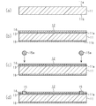
- membrane of 1st Embodiment. 2-2 line sectional drawing of FIG. (A)-(d) is explanatory drawing which shows the manufacturing method of glass with a film
- (A)-(c) is explanatory drawing of the laminated structure of the multilayer film of Examples 1-3
- (d) is a graph which shows the relationship of the wavelength of the light and the reflectance which were irradiated to the glass plate with a film
- the film-coated glass 10 ⁇ / b> A of the first embodiment includes a plate-like translucent glass substrate 11.
- the thickness of the glass substrate 11 is, for example, 0.05 to 5 mm.
- known glasses such as non-alkali glass, aluminosilicate glass, soda lime glass and the like can be used.
- tempered glass such as chemically strengthened glass or crystallized glass such as LAS-based crystallized glass can be used.
- an aluminosilicate glass in particular, SiO 2 : 50 to 80% by mass, Al 2 O 3 : 5 to 25% by mass, B 2 O 3 : 0 to 15% by mass, Na 2 O: 1 It is preferable to use a chemically strengthened glass containing ⁇ 20 mass% and K 2 O: 0 ⁇ 10 mass%.
- a multilayer film 12 is provided on one main surface 11 a of the glass substrate 11. As shown in FIG. 2, the multilayer film 12 has a laminated structure in which a transparent conductive film 13 and an antireflection film 14 as an insulating film are located in order from the main surface 11 a side of the glass substrate 11. Therefore, the transparent conductive film 13 is provided closer to the glass substrate 11 than the antireflective film 14.
- the transparent conductive film 13 functions as a heating element that generates heat when energized.
- the material which comprises the transparent conductive film 13 will not be specifically limited if it has translucency and electroconductivity.
- Examples of the material constituting the transparent conductive film 13 include, for example, indium tin oxide, fluorine-doped tin oxide, indium zinc oxide, aluminum-doped zinc oxide, tin oxide, zinc oxide, indium oxide, antimony-doped indium oxide, titanium oxide It can be mentioned. Among these, indium tin oxide having a low resistance value and a large calorific value is preferable.
- the thickness of the transparent conductive film 13 is, for example, preferably 25 nm or more, and more preferably 125 nm or more. By forming the transparent conductive film 13 thick, a high calorific value can be easily obtained. Further, from the viewpoint of securing the light transmittance, the thickness of the transparent conductive film 13 is preferably 500 nm or less.
- the antireflective film 14 is a film for reflecting specific light such as visible light, and has a structure in which a high refractive index film and a low refractive index film having a refractive index lower than that of the high refractive index film are alternately stacked. It has a dielectric multilayer film.
- the material constituting the high refractive index film include, for example, at least one selected from niobium oxide, titanium oxide, tantalum oxide, lanthanum oxide, tungsten oxide, and zirconium oxide.
- the high refractive index film preferably contains niobium oxide.
- the material constituting the low refractive index film include, for example, at least one selected from silicon oxide and aluminum oxide.
- the low refractive index film preferably contains silicon oxide.
- the transparent conductive film 13 is an indium tin oxide film (ITO film)
- ITO film indium tin oxide film
- the anti-reflection film 14 so as to be a so-called IMITO film (Index Matched ITO film).
- the film in contact with the transparent conductive film 13 may be either a high refractive index film or a low refractive index film, but is preferably a low refractive index film.
- the thickness of the anti-reflection film 14 is, for example, 200 to 4000 nm.
- the total number of stacked layers of the high refractive index film and the low refractive index film in the antireflective film 14 is, for example, 4 to 60 layers.
- a dielectric multilayer film having a laminated structure shown in FIG. 6A can be mentioned.
- the wavelength of light whose reflection is prevented by the antireflective film 14 is not particularly limited.
- the laminated structure of the dielectric multilayer film is designed according to the wavelength of light to be prevented from being reflected.
- the antireflective film 14 may have a transition layer in which the refractive index gradually decreases or increases from the high refractive index film toward the low refractive index film, between the high refractive index film and the low refractive index film. .
- the antireflective film 14 may have a transition layer in which the refractive index gradually decreases toward the transparent conductive film 13 in the portion on the transparent conductive film 13 side.
- the antireflection film 14 may have a medium refractive index film whose refractive index is smaller than that of the high refractive index film and larger than that of the low refractive index film.
- the film-coated glass 10 ⁇ / b> A includes a pair of electrodes 15 for energizing the transparent conductive film 13.
- the electrode 15 is provided so that the whole is located inside the peripheral edges of the glass substrate 11 and the multilayer film 12 in a plan view shown in FIG. Then, as shown in FIG. 2, in the stacking direction of the multilayer film 12, the electrode 15 penetrates the multilayer film 12, and one end (the lower portion in FIG. 2) is joined to the glass substrate 11, In FIG. 2, the upper part is exposed from the surface of the multilayer film 12.
- the electrode 15 is made of solder and is joined to the major surface 11 a of the glass substrate 11 by ultrasonic soldering.
- the kind of solder which comprises the electrode 15 is not specifically limited, The well-known solder which can be ultrasonically soldered can be used.
- an anti-reflection film 16 is provided on the other main surface 11 b of the glass substrate 11.
- the antireflective film 16 is made of the same dielectric multilayer film as the antireflective film 14.
- the film-coated glass 10A Since the film-coated glass 10A generates heat when current is applied to the transparent conductive film 13 through the electrode 15, it can be applied, for example, as a cover glass having an antifogging function.
- cover glass having an antifogging function.
- applications of the above cover glass include, for example, camera applications (eg, CMOS cameras, CCD cameras), and frozen showcase applications.
- the film-coated glass 10A is manufactured by sequentially performing a film forming process and an electrode forming process described below.
- the film forming step is a step of forming the multilayer film 12 on the glass substrate 11.
- the transparent conductive film 13 is formed on one main surface 11 a of the glass substrate 11 using a known film forming method.
- the method for forming the transparent conductive film 13 include known film forming methods such as a sputtering method, a vacuum evaporation method, an ion beam method, an ion plating method, and a CVD method.
- the sputtering method is preferable because the layer thickness can be controlled with high accuracy and the transparent conductive film 13 with stable film quality can be obtained.
- each layer of the anti-reflection film 14 is sequentially formed on the upper surface of the transparent conductive film 13 using a known film forming method.
- the method for forming the antireflective film 14 include known film forming methods such as sputtering, vacuum evaporation, ion beam, ion plating, and CVD.
- the sputtering method is preferable because the layer thickness can be controlled with high accuracy and the antireflective film 14 with stable film quality can be obtained.
- the anti-reflection film 16 is formed on the other principal surface 11 b of the glass substrate 11 using a known film forming method.
- the electrode forming step is a step of forming the electrode 15 by penetrating the multilayer film 12 in the glass substrate 11 on which the multilayer film 12 is formed.
- the electrode 15 composed of solder is joined to the glass substrate 11 by ultrasonic soldering. Specifically, molten solder 15 a in a state in which ultrasonic vibration is applied is applied to the surface of multilayer film 12.
- molten solder 15a Due to the cavitation effect of molten solder 15a, molten solder 15a penetrates anti-reflection film 14 and transparent conductive film 13 constituting multilayer film 12 to reach main surface 11a of glass substrate 11, and is bonded to glass substrate 11 .
- the heating temperature in ultrasonic soldering is preferably 120 to 400 ° C., for example.
- the film-coated glass 10A is provided on the glass substrate 11, the major surface 11a of the glass substrate 11, and the multilayer film 12 having the transparent conductive film 13 and the antireflective film 14 as the insulating film, and transparent conductive
- An electrode 15 is provided to energize the membrane 13. One end of the electrode 15 is bonded to the glass substrate 11 in the stacking direction of the multilayer film 12, and the other end is exposed from the surface of the multilayer film 12.
- the lead wire 17 to the electrode 15 from the surface side of the multilayer film 12 by a method such as printing or soldering, as indicated by a phantom line (one-dot chain line) in FIG. is there.
- a phantom line one-dot chain line
- the film-coated glass 10A is used by being held by a holding member such as a casing, a terminal is provided on the holding portion of the holding member, and the terminal is brought into contact with the electrode 15 exposed on the surface side of the multilayer film 12 It is also possible to connect the terminal and the electrode 15. Therefore, a lead wire or the like can be easily connected to the electrode 15.
- the electrode 15 can be exposed on the surface of the multilayer film 12 without being affected by the multilayer structure of the multilayer film 12, the degree of freedom in designing the multilayer structure of the multilayer film 12 is improved. That is, the laminated structure of the multilayer film 12 can be designed without considering the configuration for connecting the lead wires and the like. For example, it is easy to make the transparent conductive film 13 and the antireflective film 14 into an IMITO film.
- the electrodes other than the periphery of the glass substrate 11 and the multilayer film 12 are electrodes Also in the case where the wiring 15 is disposed, a lead wire or the like can be connected to the electrode 15 from the surface side of the multilayer film 12. Therefore, the degree of freedom in the arrangement of the electrodes 15 in the surface direction of the film-coated glass 10A is improved.
- the electrode 15 is directly bonded to the glass substrate 11, so that the electrode 15 is less likely to be detached from the glass substrate 11 can get.
- the peripheral portion of the filmed glass is suitable as a holding portion for holding the filmed glass by a holding member such as a casing.
- a holding member such as a casing.
- an electrode is disposed at the peripheral portion of the film-coated glass in consideration of connection to a lead wire or the like, it is difficult to use the portion as the holding portion because it easily interferes with the lead wire or the like.
- the filmed glass 10A of the present embodiment since the electrode 15 is disposed avoiding the peripheral portion of the filmed glass, the peripheral portion of the filmed glass is used as the holding portion or for other purposes. Is easy.
- the transparent conductive film 13 is positioned closer to the glass substrate 11 than the antireflective film 14 as the insulating film. According to the above configuration, compared to the configuration in which the antireflective film 14 is located closer to the glass substrate 11 than the transparent conductive film 13 and the transparent conductive film 13 is located on the surface of the multilayer film 12, the reflectance is Can be lowered.
- the multilayer film 12 is penetrated through the film forming step of forming the multilayer film 12 on the glass substrate 11 and the glass substrate 11 on which the multilayer film 12 is formed.
- an electrode forming step of forming The electrode forming step is a step of bonding the electrode 15 composed of the solder to the glass substrate 11 by ultrasonic soldering from the surface side of the multilayer film 12.
- the insulating film (reflection) is particularly outside the transparent conductive film 13 (that is, farther from the glass substrate 11 than the transparent conductive film 13) without being affected by the laminated structure of the multilayer film 12 Even when the protective film 14) is positioned, the film-coated glass 10A in which the electrode 15 is exposed from the surface of the multilayer film 12 can be manufactured.
- the film-coated glass 10A since it is not necessary to perform processing such as masking the portion where the electrode 15 is disposed in the multilayer film formation step, the film-coated glass 10A can be easily manufactured.
- the second embodiment of the film-coated glass will be described focusing on differences from the first embodiment.
- the configuration of the multilayer film 12 is different from that of the first embodiment.
- an antireflective film 14a, a transparent conductive film 13, and an antireflective film 14b are formed in order from the main surface 11a side of the glass substrate 11. Therefore, on the side of the glass substrate 11 relative to the transparent conductive film 13 and on the opposite side (that is, a position closer to the glass substrate 11 than the transparent conductive film 13 and a position farther from the glass substrate 11 than the transparent conductive film 13)
- the anti-reflective film 14 (14a, 14b) is provided in each.
- Each of the antireflection films 14a and 14b is formed of a dielectric multilayer film, a high refractive index film, or a low refractive index film having a structure in which the high refractive index film and the low refractive index film are alternately stacked. .
- the thickness of each of the antireflective films 14a and 14b is, for example, 5 to 4000 nm.
- the total number of stacked layers of all the high refractive index films and low refractive index films including the antireflective films 14a and 14b is, for example, 4 to 60 layers.
- the number of stacked layers of each of the antireflective films 14a and 14b is one or more.
- the multilayer film 12 of the glass 10B with a film the multilayer film of the laminated structure shown to FIG. 6B is mentioned, for example.
- the multilayer film 12 may be formed in the order of the antireflective film 14a, the transparent conductive film 13 and the antireflective film 14b in the above film forming step.
- the antireflective films 14a and 14b are provided on the side of the glass substrate 11 relative to the transparent conductive film 13 and on the opposite side.
- the reflectance is higher than when the antireflective films 14a and 14b are formed on the opposite side of the transparent conductive film 13 to the side opposite to the glass substrate 11 (the film-coated glass 10A of the first embodiment) Can be lowered. Therefore, the reflectance can be reduced while reducing the overall thickness of the multilayer film 12.
- the above effect is particularly effective when the transparent conductive film 13 is formed thick (for example, when the thickness is 125 nm or more).
- the reason why the above effect can be obtained is that, in the case where the transparent conductive film 13 is formed thick and the thick transparent conductive film 13 is in contact with the glass substrate 11, the glass substrate 11 is interfered by light interference therebetween. It is considered that the reflectance is not sufficiently lowered only with the anti-reflection film 14b located on the opposite side to the above.
- the multilayer film 12 As shown in FIG. 5, in the multilayer film 12 of the film-coated glass 10C, the antireflective film 14a, the transparent conductive film 13a, the antireflective film 14b, the transparent conductive film 13b, and so on from the main surface 11a side of the glass substrate 11. And the anti-reflective film 14c is formed. Therefore, the multilayer film 12 has a plurality (two layers in this embodiment) of transparent conductive films 13 (13a, 13b) separated by the antireflective films 14 (14a, 14b, 14c) in the laminating direction. There is.
- each transparent conductive film 13 13a, 13b
- the anti-reflective film 14 14a, 14b, 14c is provided in each of the position away from.
- the transparent conductive films 13a and 13b may be the same transparent conductive film or different transparent conductive films.
- Each of the anti-reflection films 14a, 14b and 14c is composed of a dielectric multilayer film having a structure in which the high refractive index film and the low refractive index film are alternately stacked, the high refractive index film, or the low refractive index film. Be done.
- the thickness of each of the antireflective films 14a, 14b and 14c is, for example, 5 to 4000 nm.
- the total number of stacked layers of all the high refractive index films and low refractive index films including the antireflective films 14a, 14b and 14c is, for example, 4 to 60.
- the number of stacked layers of each of the antireflective films 14a, 14b and 14c is one or more.
- the multilayer film 12 of the film-coated glass 10C for example, a multilayer film having a laminated structure shown in FIG.
- the multilayer film 12 is formed in the order of the antireflective film 14a, the transparent conductive film 13a, the antireflective film 14b, the transparent conductive film 13b, and the antireflective film 14c in the above film forming step. Form.
- the multilayer film 12 has a plurality of transparent conductive films 13a and 13b separated by an insulating film (antireflection film 14b) in the stacking direction.
- one end is bonded to the glass substrate 11 and the other end (the upper portion in FIG. 5) is exposed from the surface of the multilayer film 12 in the stacking direction of the multilayer film 12.
- the electrode 15 is in contact with both of the transparent conductive films 13a and 13b. Therefore, the electrodes 15 to be energized to the transparent conductive films 13a and 13b can be made common, and it is not necessary to provide separate electrodes 15. Therefore, the configuration of the electrode 15 having one end joined to the glass substrate 11 and the other end exposed from the surface of the multilayer film 12 is combined with the configuration having a plurality of transparent conductive films 13 separated by an insulating film. Particularly effective.
- the antireflective films 14a, 14b and 14c are provided on the side of the glass substrate 11 and the opposite side of the transparent conductive films 13a and 13b. According to the above configuration, the same effect as the above (5) can be obtained.
- the film-coated glass 10A is connected to a portion of the electrode 15 exposed from the surface of the multilayer film 12 as indicated by a phantom line (one-dot chain line) in FIG. 17 may be provided.
- a phantom line one-dot chain line
- the multilayer film 12 may have a laminated structure in which the transparent conductive film 13 is positioned closest to the surface (the side opposite to the glass substrate 11).
- the multilayer film 12 may have other films than the transparent conductive film 13 and the antireflective film 14. Examples of other films include, for example, an antifouling film for preventing adhesion of dirt, and a protective film for preventing scratching and corrosion.
- the multilayer film 12 may have an insulating film other than the antireflective film 14. In the case where the other films have insulating properties, the films are also included in the insulating film.
- the multilayer film 12 includes a plurality of insulating films, at least one insulating film is positioned outside the transparent conductive film 13 (that is, the glass substrate than the transparent conductive film 13). Preferably located away from 11). Further, when the multilayer film 12 has an insulating film other than the antireflective film 14, the antireflective film 14 may be omitted.
- the antireflective film 14 is not limited to the dielectric multilayer film, and may be another known antireflective film.
- the transparent conductive film 13a may be provided on the main surface 11a of the glass substrate 11 without an insulating film such as the antireflective film 14 being interposed.
- the surface treatment to be applied to the other principal surface 11b of the glass substrate 11 is not particularly limited.
- a film other than the antireflective film 16 may be provided, or the antireflective film 16 may be omitted.
- the multilayer film 12 may be provided on the major surface 11 b of the glass substrate 11.
- the formation position of the electrode 15 is not particularly limited.
- the electrode 15 may be formed at a position along the periphery of the glass substrate 11 or the insulating film.
- the shape of the electrode 15 is not particularly limited.
- the electrode 15 may be formed to be flush with the surface of the multilayer film 12 or may be formed to project beyond the surface of the multilayer film 12.
- the material which comprises the electrode 15 is not limited to a solder.
- the electrode 15 may be formed using a known conductive material used as an electrode such as silver paste.
- a film-coated glass of Example 1 was produced by forming a multilayer film of the laminated structure shown in FIG. 6 (a) on one main surface of a glass substrate (manufactured by Nippon Electric Glass Co., Ltd .: OA-10G).
- the transparent conductive film constituting the multilayer film is an ITO film.
- the ITO film was formed using an ITO target using a magnetron sputtering apparatus (ANELVA SPC-350) under the conditions of Ar: 40 sccm, O 2 : 1 sccm, power: 150 W, and substrate temperature 250 ° C.
- the antireflection film constituting the multilayer film is a dielectric multilayer film comprising a plurality of niobium oxide films (Nb 2 O 5 ) and a plurality of silicon oxide films (SiO 2 ), and prevents reflection of light in the visible light range It is designed as.
- a dielectric multilayer film was formed under the conditions of Ar: 20 sccm, O 2 : 15 sccm, power: 150 W, and substrate temperature 250 ° C. using the above-described apparatus.
- Example 2 In the same manner as in Example 1, a film-coated glass of Example 2 having a multilayer film having a laminated structure shown in FIG. 6B was produced.
- the second embodiment is different from the first embodiment in that a transparent conductive film is provided between two antireflection films in the multilayer structure of the multilayer film.
- Example 3 a film-coated glass of Example 3 having a multilayer film having a laminated structure shown in FIG. 6C was produced.
- the third embodiment is different from the first embodiment in that the transparent conductive film is formed in two layers and each transparent conductive film is provided between two antireflection films with respect to the laminated structure of the multilayer film.
- FIG. 6 (d) is a graph showing the relationship between the wavelength of light irradiated to the film-coated glass of Examples 1 to 3 and the reflectance of the surface of the film-coated glass on which the multilayer film is formed.
- the reflectances of the second embodiment and the third embodiment are lower than the reflectance of the first embodiment. From this result, it can be seen that reflection can be more effectively prevented by providing the anti-reflection film on each of the glass substrate side and the opposite side of the transparent conductive film.
- the above-described effect can be similarly obtained also when a plurality of transparent conductive films are provided as in the third embodiment.
- 10A, 10B, 10C Glass with film
- 11 Glass substrate
- 12 Multilayer film
- 13, 13a, 13b Transparent conductive film
- 14, 14a, 14b, 14c Antireflection film (insulation film)
- 15 Electrode
- 17 ... lead wire.
Landscapes
- Chemical & Material Sciences (AREA)
- Engineering & Computer Science (AREA)
- Materials Engineering (AREA)
- Chemical Kinetics & Catalysis (AREA)
- General Chemical & Material Sciences (AREA)
- Geochemistry & Mineralogy (AREA)
- Life Sciences & Earth Sciences (AREA)
- Organic Chemistry (AREA)
- Manufacturing & Machinery (AREA)
- Surface Treatment Of Glass (AREA)
- Non-Insulated Conductors (AREA)
- Manufacturing Of Electric Cables (AREA)
- Surface Treatment Of Optical Elements (AREA)
- Laminated Bodies (AREA)
Abstract
本発明は、電極に対して引出し線等を容易に接続することのできる膜付きガラスを提供することを課題とする。膜付きガラス(10A)は、ガラス基材(11)と、ガラス基材(11)の主面(11a)に設けられ、透明導電膜(13)、及び絶縁膜としての反射防止膜(14)を有する多層膜(12)と、透明導電膜(13)に通電する電極(15)とを備えている。電極(15)は、多層膜(12)の積層方向において、一端がガラス基材(11)に接合され、他端が多層膜(12)の表面から露出している。
Description
本発明は、膜付きガラス、及び膜付きガラスの製造方法に関する。
特許文献1に開示される膜付きガラスは、ガラス基板と、ガラス基板の主面に設けられた電極と、ガラス基板の主面及び電極の上に設けられた透明導電膜と、透明導電膜の上に設けられた反射防止膜とを備えている。こうした膜付きガラスは、防曇機能を有するカバーガラスとして、カメラや冷凍ショーケース等に適用されている。
ところで、膜付きガラスの電極には、電力を供給するための引出し線が接続されるが、特許文献1の膜付きガラスのように、電極の上に透明導電膜や反射防止膜が設けられている場合には、引出し線の形成にかかるコストが大きくなりやすい。すなわち、電極の上に透明導電膜や反射防止膜が設けられている膜付きガラスは、透明導電膜や反射防止膜の成膜前に引出し線が形成される。この場合、電極を設けたガラス基板の上にマスクを形成して引出し線を印刷することになるため、マスクを形成するマスク工程が増えてしまう。さらに、引出し線を印刷した後にガラス板を切断して最終製品を得る場合には、切断線を考慮してマスクを形成する必要がある等の理由から、マスク工程が非常に複雑になる。
この発明は、こうした実情に鑑みてなされたものであり、その目的は、電極に対して引出し線等を容易に接続することのできる膜付きガラス、及びその製造方法を提供することにある。
上記課題を解決する膜付きガラスは、ガラス基材と、前記ガラス基材の少なくとも一面に設けられ、透明導電膜及び絶縁膜を有する多層膜と、前記透明導電膜に通電する電極とを備える膜付きガラスであって、前記電極は、前記多層膜の積層方向において、一端が前記ガラス基材に接合され、他端が前記多層膜の表面から露出している。
上記構成によれば、電極における多層膜の表面から露出した部分に対して、多層膜の表面側から引出し線等を接続することが可能である。そのため、多層膜の成膜前にマスクを形成して引出し線を印刷する必要がなく、電極に対して引出し線等を容易に接続することができる。また、多層膜の積層構造に影響されることなく、多層膜の表面に電極を露出させることができるため、多層膜の積層構造を設計する際の自由度が向上する。すなわち、引出し線等を接続するための構成を考慮することなく、多層膜の積層構造を設計することができる。
上記膜付きガラスにおいて、前記電極における前記多層膜の表面から露出した部分には、引出し線が接続されていることが好ましい。
上記膜付きガラスにおいて、前記絶縁膜は、反射防止膜であることが好ましい。
上記膜付きガラスにおいて、前記絶縁膜は、反射防止膜であることが好ましい。
上記構成によれば、光の反射が少ないことが好ましい用途に好適に適用することができる。
上記膜付きガラスにおいて、前記反射防止膜は、前記多層膜の積層方向において、前記透明導電膜よりも前記ガラス基材側とその反対側のそれぞれに位置することが好ましい。
上記膜付きガラスにおいて、前記反射防止膜は、前記多層膜の積層方向において、前記透明導電膜よりも前記ガラス基材側とその反対側のそれぞれに位置することが好ましい。
上記構成によれば、透明導電膜の外側に(すなわち、透明導電膜よりもガラス基材から離れた位置において)全ての反射防止膜を重ねて形成した場合と比較して反射率を低下させることができる。したがって、多層膜の厚さを小さくしつつ反射率を低下させることができる。
上記膜付きガラスにおいて、前記多層膜は、その積層方向において、前記絶縁膜により隔てられた複数の前記透明導電膜を有していることが好ましい。
多層膜の積層方向において、一端がガラス基材に接合され、他端が多層膜の表面から露出している電極は、各透明導電膜に接触している。そのため、各透明導電膜に通電する電極を共通化することができ、それぞれ別々の電極を設ける必要がない。したがって、一端がガラス基材に接合され、他端が多層膜の表面から露出している電極の構成は、絶縁膜により隔てられた複数の透明導電膜を有する構成と組み合わせた場合に特に有効である。
多層膜の積層方向において、一端がガラス基材に接合され、他端が多層膜の表面から露出している電極は、各透明導電膜に接触している。そのため、各透明導電膜に通電する電極を共通化することができ、それぞれ別々の電極を設ける必要がない。したがって、一端がガラス基材に接合され、他端が多層膜の表面から露出している電極の構成は、絶縁膜により隔てられた複数の透明導電膜を有する構成と組み合わせた場合に特に有効である。
上記膜付きガラスの製造方法は、前記ガラス基材に前記多層膜を形成する工程と、前記多層膜が形成された前記ガラス基材に、前記多層膜を貫通させて前記電極を形成する工程とを有する。前記電極を形成する工程は、前記多層膜の表面側からの超音波はんだ付けによって、はんだにより構成される前記電極を前記ガラス基材に接合する工程であることが好ましい。
上記構成によれば、多層膜の積層構造に影響されることなく、多層膜の表面から電極が露出している膜付きガラスを容易に製造することができる。
本発明によれば、電極に対して引出し線等を容易に接続することができる。
<第1実施形態>
以下、膜付きガラスの第1実施形態について説明する。
図1及び図2に示すように、第1実施形態の膜付きガラス10Aは、板状をなす透光性のガラス基材11を備えている。ガラス基材11の厚さは、例えば、0.05~5mmである。ガラス基材11としては、例えば、無アルカリガラス、アルミノシリケートガラス、ソーダライムガラス等の公知のガラスを用いることができる。また、化学強化ガラス等の強化ガラスやLAS系結晶化ガラス等の結晶化ガラスを用いることができる。これらのなかでも、アルミノシリケートガラスを用いること、特に、SiO2:50~80質量%、Al2O3:5~25質量%、B2O3:0~15質量%、Na2O:1~20質量%、K2O:0~10質量%を含有する化学強化ガラスを用いることが好ましい。
以下、膜付きガラスの第1実施形態について説明する。
図1及び図2に示すように、第1実施形態の膜付きガラス10Aは、板状をなす透光性のガラス基材11を備えている。ガラス基材11の厚さは、例えば、0.05~5mmである。ガラス基材11としては、例えば、無アルカリガラス、アルミノシリケートガラス、ソーダライムガラス等の公知のガラスを用いることができる。また、化学強化ガラス等の強化ガラスやLAS系結晶化ガラス等の結晶化ガラスを用いることができる。これらのなかでも、アルミノシリケートガラスを用いること、特に、SiO2:50~80質量%、Al2O3:5~25質量%、B2O3:0~15質量%、Na2O:1~20質量%、K2O:0~10質量%を含有する化学強化ガラスを用いることが好ましい。
ガラス基材11の一方の主面11aには、多層膜12が設けられている。図2に示すように、多層膜12は、ガラス基材11の主面11a側から順に、透明導電膜13、絶縁膜としての反射防止膜14が位置する積層構造を有する。したがって、反射防止膜14よりもガラス基材11側に透明導電膜13が設けられている。
透明導電膜13は、通電されることにより発熱する発熱体として機能する。透明導電膜13を構成する材料は、透光性及び導電性を有するものであれば特に限定されない。透明導電膜13を構成する材料の例としては、例えば、酸化インジウムスズ、フッ素ドープ酸化錫、酸化インジウム亜鉛、アルミニウムドープ酸化亜鉛、酸化錫、酸化亜鉛、酸化インジウム、アンチモンドープ酸化インジウム、酸化チタンが挙げられる。これらのなかでも、抵抗値が低く、発熱量が大きい酸化インジウムスズが好ましい。
透明導電膜13の厚さは、例えば、25nm以上であることが好ましく、125nm以上であることがより好ましい。透明導電膜13を厚く形成することにより、高い発熱量が得られやすくなる。また、透光性を確保する観点から、透明導電膜13の厚さは、500nm以下であることが好ましい。
反射防止膜14は、可視光等の特定の光を反射するための膜であり、高屈折率膜と、高屈折率膜よりも屈折率が低い低屈折率膜とを交互に積層した構造を有する誘電体多層膜からなる。高屈折率膜を構成する材料の例としては、例えば、酸化ニオブ、酸化チタン、酸化タンタル、酸化ランタン、酸化タングステン、及び酸化ジルコニウムから選ばれる少なくとも一種が挙げられる。高屈折率膜は、酸化ニオブを含むことが好ましい。低屈折率膜を構成する材料の例としては、例えば、酸化ケイ素及び酸化アルミニウムから選ばれる少なくとも一種が挙げられる。低屈折率膜は、酸化ケイ素を含むことが好ましい。
なお、透明導電膜13が酸化インジウムスズ膜(ITO膜)である場合、いわゆるIMITO膜(Index Matched ITO膜)となるように、反射防止膜14を設計することが好ましい。また、反射防止膜14において、透明導電膜13に接する膜は、高屈折率膜及び低屈折率膜のいずれでもよいが、低屈折率膜であることが好ましい。
反射防止膜14の厚さは、例えば、200~4000nmである。反射防止膜14における高屈折率膜と低屈折率膜との合計積層数は、例えば、4~60層である。反射防止膜14の具体例としては、例えば、図6(a)に示す積層構造の誘電体多層膜が挙げられる。
なお、反射防止膜14によって反射が防止される光の波長は特に限定されるものではない。誘電体多層膜の積層構造は、反射を防止すべき光の波長に応じて設計される。また、反射防止膜14は、高屈折率膜から低屈折率膜に向けて屈折率が漸減または漸増する漸移層を高屈折率膜と低屈折率膜との間に有していてもよい。反射防止膜14は、透明導電膜13側の部分に、透明導電膜13に向けて屈折率が漸減する漸移層を有していてもよい。反射防止膜14は、屈折率が高屈折率膜よりも小さく、かつ、低屈折率膜より大きい中屈折率膜を有していてもよい。
図1及び図2に示すように、膜付きガラス10Aは、透明導電膜13に通電するための一対の電極15を備えている。電極15は、図1に示す平面視において、その全体がガラス基材11及び多層膜12の周縁よりも内側に位置するように設けられている。そして、図2に示すように、多層膜12の積層方向において、電極15は、多層膜12を貫通し、その一端(図2では下部)がガラス基材11に接合されるとともに、他端(図2では上部)が多層膜12の表面から露出している。
電極15は、はんだにより構成され、超音波はんだ付けによってガラス基材11の主面11aに接合されている。電極15を構成するはんだの種類は特に限定されるものではなく、超音波はんだ付けが可能な公知のはんだを用いることができる。
また、図2に示すように、ガラス基材11のもう一方の主面11bには、反射防止膜16が設けられている。反射防止膜16は、反射防止膜14と同様の誘電体多層膜からなる。
膜付きガラス10Aは、電極15を通じて透明導電膜13に通電することにより発熱することから、例えば、防曇機能を有するカバーガラスとして適用することができる。上記カバーガラスの用途の例としては、例えば、カメラ用途(例えば、CMOSカメラ、CCDカメラ)、及び冷凍ショーケース用途が挙げられる。
次に、膜付きガラス10Aの製造方法の一例について説明する。
膜付きガラス10Aは、以下に記載する膜形成工程、及び電極形成工程を順に経ることにより製造される。
膜付きガラス10Aは、以下に記載する膜形成工程、及び電極形成工程を順に経ることにより製造される。
図3(a)~(b)に示すように、膜形成工程は、ガラス基材11に多層膜12を形成する工程である。膜形成工程では、まず周知の成膜方法を用いて、ガラス基材11の一方の主面11aに透明導電膜13を形成する。透明導電膜13の形成方法の例としては、例えば、スパッタリング法、真空蒸着法、イオンビーム法、イオンプレーティング法、CVD法等の公知の成膜方法が挙げられる。これらの成膜方法の中でも、層の厚さを高精度で制御することができるとともに、安定した膜質の透明導電膜13が得られることから、スパッタリング法が好ましい。
そして、周知の成膜方法を用いて、透明導電膜13の上面に反射防止膜14の各層を順次形成する。反射防止膜14の形成方法の例としては、例えば、スパッタリング法、真空蒸着法、イオンビーム法、イオンプレーティング法、CVD法等の公知の成膜方法が挙げられる。これらの成膜方法の中でも、層の厚さを高精度で制御することができるとともに、安定した膜質の反射防止膜14が得られることから、スパッタリング法が好ましい。
また、膜形成工程において、周知の成膜方法を用いて、ガラス基材11のもう一方の主面11bに反射防止膜16を形成する。
図3(c)~(d)に示すように、電極形成工程は、多層膜12が形成されたガラス基材11に、多層膜12を貫通させて電極15を形成する工程である。電極形成工程では、超音波はんだ付けによって、はんだにより構成される電極15をガラス基材11に接合する。具体的には、超音波振動が付与されている状態の溶融はんだ15aを多層膜12の表面に塗布する。溶融はんだ15aのキャビテーション効果により、多層膜12を構成する反射防止膜14及び透明導電膜13を貫通して溶融はんだ15aがガラス基材11の主面11aに達し、ガラス基材11に接合される。なお、超音波はんだ付けにおける加熱温度は、例えば、120~400℃であることが好ましい。
図3(c)~(d)に示すように、電極形成工程は、多層膜12が形成されたガラス基材11に、多層膜12を貫通させて電極15を形成する工程である。電極形成工程では、超音波はんだ付けによって、はんだにより構成される電極15をガラス基材11に接合する。具体的には、超音波振動が付与されている状態の溶融はんだ15aを多層膜12の表面に塗布する。溶融はんだ15aのキャビテーション効果により、多層膜12を構成する反射防止膜14及び透明導電膜13を貫通して溶融はんだ15aがガラス基材11の主面11aに達し、ガラス基材11に接合される。なお、超音波はんだ付けにおける加熱温度は、例えば、120~400℃であることが好ましい。
次に、本実施形態の作用及び効果について記載する。
(1)膜付きガラス10Aは、ガラス基材11と、ガラス基材11の主面11aに設けられ、透明導電膜13、及び絶縁膜としての反射防止膜14を有する多層膜12と、透明導電膜13に通電する電極15とを備えている。電極15は、多層膜12の積層方向において、一端がガラス基材11に接合され、他端が多層膜12の表面から露出している。
(1)膜付きガラス10Aは、ガラス基材11と、ガラス基材11の主面11aに設けられ、透明導電膜13、及び絶縁膜としての反射防止膜14を有する多層膜12と、透明導電膜13に通電する電極15とを備えている。電極15は、多層膜12の積層方向において、一端がガラス基材11に接合され、他端が多層膜12の表面から露出している。
上記構成によれば、図1の仮想線(一点鎖線)で示すように、電極15に対して多層膜12の表面側から印刷やはんだ付け等の方法により引出し線17を接続することが可能である。また、膜付きガラス10Aをケーシング等の保持部材に保持させて用いる場合には、保持部材の保持部分に端子を設け、多層膜12の表面側に露出する電極15に上記端子を接触させて、上記端子と電極15とを接続することも可能である。したがって、電極15に対して引出し線等を容易に接続することができる。
また、多層膜12の積層構造に影響されることなく、多層膜12の表面に電極15を露出させることができるため、多層膜12の積層構造を設計する際の自由度が向上する。すなわち、引出し線等を接続するための構成を考慮することなく、多層膜12の積層構造を設計することができる。例えば、透明導電膜13及び反射防止膜14をIMITO膜とすることが容易である。
また、膜付きガラス10Aの面方向(膜付きガラス10Aの厚さ方向に直交する方向、すなわち、膜付きガラス10Aの面内)において、ガラス基材11や多層膜12の周縁以外の部分に電極15を配置した場合にも、多層膜12の表面側から電極15に引出し線等を接続することができる。そのため、膜付きガラス10Aの面方向における電極15の配置の自由度が向上する。
また、多層膜12の積層構造によっては、多層膜12を構成する最表面の膜に対して電極15を接合することにより、多層膜12の表面から電極15を露出させることは可能である。こうした構成と比較して、上記実施形態の構成によれば、ガラス基材11に対して電極15が直接、接合されていることにより、ガラス基材11から電極15が脱離し難くなるという効果も得られる。
(2)膜付きガラス10Aの面方向(膜付きガラス10Aの厚さ方向に直交する方向、すなわち、膜付きガラス10Aの面内)において、ガラス基材11及び多層膜12の周縁よりも内側に電極15が位置している。
膜付きガラスの周縁部分は、ケーシング等の保持部材により膜付きガラスを保持するための保持部分として適している。しかしながら、引出し線等に接続することを考慮して膜付きガラスの周縁部分に電極を配置した場合には、引出し線等と干渉し易いことから、当該部分を上記保持部分として利用することが難しくなる。本実施形態の膜付きガラス10Aによれば、膜付きガラスの周縁部分を避けて電極15が配置されているため、膜付きガラスの周縁部分を上記保持部分として、又はその他の目的に利用することが容易である。
(3)多層膜12において、絶縁膜としての反射防止膜14よりもガラス基材11側に透明導電膜13が位置している。
上記構成によれば、透明導電膜13よりもガラス基材11側に反射防止膜14が位置して、多層膜12の表面に透明導電膜13が位置している構成と比較して、反射率を低下させることができる。
上記構成によれば、透明導電膜13よりもガラス基材11側に反射防止膜14が位置して、多層膜12の表面に透明導電膜13が位置している構成と比較して、反射率を低下させることができる。
(4)膜付きガラス10Aの製造方法は、ガラス基材11に多層膜12を形成する膜形成工程と、多層膜12が形成されたガラス基材11に、多層膜12を貫通させて電極15を形成する電極形成工程とを有している。電極形成工程は、多層膜12の表面側からの超音波はんだ付けによって、はんだにより構成される電極15をガラス基材11に接合する工程である。
上記構成によれば、多層膜12の積層構造に影響されることなく、特に、透明導電膜13よりも外側に(すなわち、透明導電膜13よりもガラス基材11から離れて)絶縁膜(反射防止膜14)が位置している場合であっても、多層膜12の表面から電極15が露出している膜付きガラス10Aを製造することができる。また、多層膜形成工程において、電極15を配置する部分をマスクする等の処理を行う必要が無いため、膜付きガラス10Aを容易に製造することができる。
<第2実施形態>
以下、膜付きガラスの第2実施形態について、第1実施形態との相違点を中心に説明する。第2実施形態の膜付きガラス10Bは、多層膜12の構成が第1実施形態と相違している。
以下、膜付きガラスの第2実施形態について、第1実施形態との相違点を中心に説明する。第2実施形態の膜付きガラス10Bは、多層膜12の構成が第1実施形態と相違している。
図4に示すように、膜付きガラス10Bの多層膜12は、ガラス基材11の主面11a側から順に、反射防止膜14a、透明導電膜13、反射防止膜14bが形成されている。したがって、透明導電膜13よりもガラス基材11側とその反対側(すなわち、透明導電膜13よりもガラス基材11に近い位置と透明導電膜13よりもガラス基材11から離れた位置)のそれぞれに反射防止膜14(14a,14b)が設けられている。
各反射防止膜14a,14bは、上記高屈折率膜と上記低屈折率膜とを交互に積層した構造を有する誘電体多層膜、上記高屈折率膜、又は上記低屈折率膜により構成される。各反射防止膜14a,14bの厚さは、例えば、5~4000nmである。反射防止膜14a,14bを合わせた全ての高屈折率膜及び低屈折率膜の合計積層数は、例えば、4~60層である。なお、反射防止膜14a,14bそれぞれの積層数は1層以上である。
膜付きガラス10Bの多層膜12の具体例としては、例えば、図6(b)に示す積層構造の多層膜が挙げられる。なお、膜付きガラス10Bを製造する場合には、上記の膜形成工程において、反射防止膜14a、透明導電膜13、反射防止膜14bの順で多層膜12を形成すればよい。
次に、本実施形態の作用及び効果について記載する。
(5)多層膜12において、反射防止膜14a,14bは、透明導電膜13よりもガラス基材11側とその反対側のそれぞれに設けられている。
(5)多層膜12において、反射防止膜14a,14bは、透明導電膜13よりもガラス基材11側とその反対側のそれぞれに設けられている。
上記構成によれば、透明導電膜13よりもガラス基材11とは反対側に反射防止膜14a,14bを重ねて形成した場合(第1実施形態の膜付きガラス10A)と比較して反射率を低下させることができる。したがって、多層膜12全体の厚さを小さくしつつ反射率を低下させることができる。上記効果は、透明導電膜13が厚く形成されている場合(例えば、厚さ125nm以上の場合)に特に有効である。上記効果の得られる理由は、透明導電膜13が厚く形成されており、かつ、厚い透明導電膜13がガラス基材11と接している場合、それらの間の光の干渉により、ガラス基材11とは反対側に位置する反射防止膜14bのみでは反射率が十分に低下しないためと考えられる。
<第3実施形態>
以下、膜付きガラスの第3実施形態について、第1実施形態との相違点を中心に説明する。第3実施形態の膜付きガラス10Cは、多層膜12の構成が第1実施形態と相違している。
以下、膜付きガラスの第3実施形態について、第1実施形態との相違点を中心に説明する。第3実施形態の膜付きガラス10Cは、多層膜12の構成が第1実施形態と相違している。
図5に示すように、膜付きガラス10Cの多層膜12においては、ガラス基材11の主面11a側から順に、反射防止膜14a、透明導電膜13a、反射防止膜14b、透明導電膜13b、及び反射防止膜14cが形成されている。したがって、多層膜12は、その積層方向において、反射防止膜14(14a,14b,14c)により隔てられた複数(本実施形態では2層)の透明導電膜13(13a,13b)を有している。また、各透明導電膜13(13a,13b)よりもガラス基材11側とその反対側(すなわち、透明導電膜13よりもガラス基材11に近い位置と透明導電膜13よりもガラス基材11から離れた位置)のそれぞれに反射防止膜14(14a,14b,14c)が設けられている。
透明導電膜13a,13bは、同じ透明導電膜であってもよいし、異なる透明導電膜であってもよい。
各反射防止膜14a,14b,14cは、上記高屈折率膜と上記低屈折率膜とを交互に積層した構造を有する誘電体多層膜、上記高屈折率膜、又は上記低屈折率膜により構成される。各反射防止膜14a,14b,14cの厚さは、例えば、5~4000nmである。反射防止膜14a,14b,14cを合わせた全ての高屈折率膜及び低屈折率膜の合計積層数は、例えば、4~60層である。なお、反射防止膜14a,14b,14cそれぞれの積層数は1層以上である。
各反射防止膜14a,14b,14cは、上記高屈折率膜と上記低屈折率膜とを交互に積層した構造を有する誘電体多層膜、上記高屈折率膜、又は上記低屈折率膜により構成される。各反射防止膜14a,14b,14cの厚さは、例えば、5~4000nmである。反射防止膜14a,14b,14cを合わせた全ての高屈折率膜及び低屈折率膜の合計積層数は、例えば、4~60層である。なお、反射防止膜14a,14b,14cそれぞれの積層数は1層以上である。
膜付きガラス10Cの多層膜12の具体例としては、例えば、図6(c)に示す積層構造の多層膜が挙げられる。なお、膜付きガラス10Cを製造する場合には、上記の膜形成工程において、反射防止膜14a、透明導電膜13a、反射防止膜14b、透明導電膜13b、反射防止膜14cの順で多層膜12を形成すればよい。
次に、本実施形態の作用及び効果について記載する。
(6)多層膜12は、その積層方向において、絶縁膜(反射防止膜14b)により隔てられた複数の透明導電膜13a,13bを有している。
(6)多層膜12は、その積層方向において、絶縁膜(反射防止膜14b)により隔てられた複数の透明導電膜13a,13bを有している。
図5に示すように、多層膜12の積層方向において、一端(図5では下部)がガラス基材11に接合され、他端(図5では上部)が多層膜12の表面から露出している電極15は、透明導電膜13a,13bの両方に接触している。そのため、透明導電膜13a,13bに通電する電極15を共通化することができ、それぞれ別々の電極15を設ける必要がない。したがって、一端がガラス基材11に接合され、他端が多層膜12の表面から露出している電極15の構成は、絶縁膜により隔てられた複数の透明導電膜13を有する構成と組み合わせた場合に特に有効である。
(7)多層膜12において、反射防止膜14a,14b,14cは、透明導電膜13a,13bよりもガラス基材11側とその反対側のそれぞれに設けられている。
上記構成によれば、上記(5)と同様の効果が得られる。
上記構成によれば、上記(5)と同様の効果が得られる。
なお、本実施形態は、次のように変更して具体化することも可能である。
・第1実施形態において、膜付きガラス10Aは、図1の仮想線(一点鎖線)で示すように、電極15における多層膜12の表面から露出した部分に接続されて、電極15から延びる引出し線17を備えるものであってもよい。第2及び第3実施形態においても同様である。
・第1実施形態において、膜付きガラス10Aは、図1の仮想線(一点鎖線)で示すように、電極15における多層膜12の表面から露出した部分に接続されて、電極15から延びる引出し線17を備えるものであってもよい。第2及び第3実施形態においても同様である。
・多層膜12は、最も表面側(ガラス基材11とは反対側)に透明導電膜13が位置する積層構造であってもよい。
・多層膜12は、透明導電膜13及び反射防止膜14以外のその他の膜を有していてもよい。その他の膜の例としては、例えば、汚れの付着を防止するための防汚膜、傷付きや腐食等を防止するための保護膜が挙げられる。
・多層膜12は、透明導電膜13及び反射防止膜14以外のその他の膜を有していてもよい。その他の膜の例としては、例えば、汚れの付着を防止するための防汚膜、傷付きや腐食等を防止するための保護膜が挙げられる。
・多層膜12は、反射防止膜14以外の絶縁膜を有していてもよい。上記その他の膜が絶縁性を有する場合には、当該膜も絶縁膜に含まれる。そして、多層膜12が複数の絶縁膜が有している場合には、少なくとも1つの絶縁膜が透明導電膜13よりも外側に位置していること(すなわち、透明導電膜13よりもガラス基材11から離れて位置していること)が好ましい。また、多層膜12が反射防止膜14以外の絶縁膜を有している場合には、反射防止膜14を省略してもよい。
・反射防止膜14は、誘電体多層膜に限定されるものではなく、その他の公知の反射防止膜であってもよい。
・上記第3実施形態において、ガラス基材11の主面11aに、反射防止膜14等の絶縁膜を介することなく透明導電膜13aが設けられていてもよい。
・上記第3実施形態において、ガラス基材11の主面11aに、反射防止膜14等の絶縁膜を介することなく透明導電膜13aが設けられていてもよい。
・ガラス基材11のもう一方の主面11bに施される表面処理は、特に限定されるものではない。例えば、反射防止膜16以外の被膜を設けてもよいし、反射防止膜16を省略してもよい。また、ガラス基材11の主面11bにも多層膜12を設けてもよい。
・電極15の形成位置は特に限定されるものではない。例えば、ガラス基材11や絶縁膜の周縁に沿う位置に電極15が形成されていてもよい。
・電極15の形状は特に限定されるものではない。例えば、電極15は、多層膜12の表面に対して面一となるように形成されていてもよいし、多層膜12の表面よりも突出するように形成されていてもよい。
・電極15の形状は特に限定されるものではない。例えば、電極15は、多層膜12の表面に対して面一となるように形成されていてもよいし、多層膜12の表面よりも突出するように形成されていてもよい。
・電極15を構成する材料は、はんだに限定されるものではない。例えば、銀ペーストのような電極として用いられる公知の導電性材料を用いて電極15を形成してもよい。
以下に実施例を挙げ、上記実施形態をさらに具体的に説明する。なお、本発明はこれらに限定されるものではない。
ガラス基材(日本電気硝子社製:OA-10G)の一方の主面に、図6(a)に示す積層構造の多層膜を形成することにより、実施例1の膜付きガラスを作製した。多層膜を構成する透明導電膜はITO膜である。ITO膜は、マグネトロンスパッタリング装置(ANELVA SPC-350)を用いて、ITOターゲットを使用し、Ar:40sccm、O2:1sccm、電力:150W、基材温度250℃の条件で形成した。多層膜を構成する反射防止膜は、複数の酸化ニオブ膜(Nb2O5)及び複数の酸化ケイ素膜(SiO2)からなる誘電体多層膜であり、可視光域の光の反射を防止するように設計されている。誘電体多層膜は、上記の装置を用いて、Ar:20sccm、O2:15sccm、電力:150W、基材温度250℃の条件で形成した。
ガラス基材(日本電気硝子社製:OA-10G)の一方の主面に、図6(a)に示す積層構造の多層膜を形成することにより、実施例1の膜付きガラスを作製した。多層膜を構成する透明導電膜はITO膜である。ITO膜は、マグネトロンスパッタリング装置(ANELVA SPC-350)を用いて、ITOターゲットを使用し、Ar:40sccm、O2:1sccm、電力:150W、基材温度250℃の条件で形成した。多層膜を構成する反射防止膜は、複数の酸化ニオブ膜(Nb2O5)及び複数の酸化ケイ素膜(SiO2)からなる誘電体多層膜であり、可視光域の光の反射を防止するように設計されている。誘電体多層膜は、上記の装置を用いて、Ar:20sccm、O2:15sccm、電力:150W、基材温度250℃の条件で形成した。
実施例1と同様にして、図6(b)に示す積層構造の多層膜を有する実施例2の膜付きガラスを作製した。実施例2は、多層膜の積層構造に関して、2つの反射防止膜の間に透明導電膜を設けている点が実施例1と異なっている。
また、実施例1と同様にして、図6(c)に示す積層構造の多層膜を有する実施例3の膜付きガラスを作製した。実施例3は、多層膜の積層構造に関して、透明導電膜を2層にするとともに、各透明導電膜を2つの反射防止膜の間に設けている点が実施例1と異なっている。
図6(d)は、実施例1~3の膜付きガラスに照射した光の波長と、膜付きガラスにおける多層膜が形成されている面の反射率との関係を示すグラフである。図6(d)に示すように、実施例2及び実施例3の反射率は、実施例1の反射率よりも低くなっている。この結果から、透明導電膜よりもガラス基材側とその反対側のそれぞれに反射防止膜を設けることによって、より効果的に反射を防止できることが分かる。また、上記効果は、実施例3のように透明導電膜を複数設けた場合にも同様に得られることが分かる。
10A,10B,10C…膜付きガラス、11…ガラス基材、12…多層膜、13,13a,13b…透明導電膜、14,14a,14b,14c…反射防止膜(絶縁膜)、15…電極、16…反射防止膜、17…引出し線。
Claims (7)
- ガラス基材と、
前記ガラス基材の少なくとも一面に設けられ、透明導電膜及び絶縁膜を有する多層膜と、
前記透明導電膜に通電する電極とを備える膜付きガラスであって、
前記電極は、前記多層膜の積層方向において、一端が前記ガラス基材に接合され、他端が前記多層膜の表面から露出していることを特徴とする膜付きガラス。 - 前記電極における前記多層膜の表面から露出した部分には、引出し線が接続されていることを特徴とする請求項1に記載の膜付きガラス。
- 前記絶縁膜は、反射防止膜であることを特徴とする請求項1又は請求項2に記載の膜付きガラス。
- 前記反射防止膜は、前記多層膜の積層方向において、前記透明導電膜よりも前記ガラス基材側とその反対側のそれぞれに位置することを特徴とする請求項3に記載の膜付きガラス。
- 前記多層膜は、その積層方向において、前記絶縁膜により隔てられた複数の前記透明導電膜を有していることを特徴とする請求項1~4のいずれか一項に記載の膜付きガラス。
- 請求項1~5のいずれか一項に記載の膜付きガラスの製造方法であって、
前記ガラス基材に前記多層膜を形成する工程と、
前記多層膜が形成された前記ガラス基材に、前記多層膜を貫通させて前記電極を形成する工程とを有することを特徴とする膜付きガラスの製造方法。 - 前記電極を形成する工程は、前記多層膜の表面側からの超音波はんだ付けによって、はんだにより構成される前記電極を前記ガラス基材に接合する工程であることを特徴とする請求項6に記載の膜付きガラスの製造方法。
Applications Claiming Priority (2)
| Application Number | Priority Date | Filing Date | Title |
|---|---|---|---|
| JP2017-126624 | 2017-06-28 | ||
| JP2017126624A JP2019006656A (ja) | 2017-06-28 | 2017-06-28 | 膜付きガラス、及び膜付きガラスの製造方法 |
Publications (1)
| Publication Number | Publication Date |
|---|---|
| WO2019004002A1 true WO2019004002A1 (ja) | 2019-01-03 |
Family
ID=64740685
Family Applications (1)
| Application Number | Title | Priority Date | Filing Date |
|---|---|---|---|
| PCT/JP2018/023250 Ceased WO2019004002A1 (ja) | 2017-06-28 | 2018-06-19 | 膜付きガラス、及び膜付きガラスの製造方法 |
Country Status (2)
| Country | Link |
|---|---|
| JP (1) | JP2019006656A (ja) |
| WO (1) | WO2019004002A1 (ja) |
Cited By (1)
| Publication number | Priority date | Publication date | Assignee | Title |
|---|---|---|---|---|
| WO2024200591A1 (en) * | 2023-03-31 | 2024-10-03 | Agp Worldwide Operations Gmbh | Glazing with low emissivity coating and enhanced bendability |
Citations (4)
| Publication number | Priority date | Publication date | Assignee | Title |
|---|---|---|---|---|
| JPH08287850A (ja) * | 1995-02-14 | 1996-11-01 | Sony Corp | 陰極線管、表示装置および陰極線管の製造方法 |
| JPH10101378A (ja) * | 1996-09-26 | 1998-04-21 | Sun Tec Corp Kk | 導電性加熱板およびその製造方法 |
| JP2006202626A (ja) * | 2005-01-21 | 2006-08-03 | Seiko Epson Corp | 光学薄膜及び光学薄膜の成膜方法 |
| JP2008159534A (ja) * | 2006-12-26 | 2008-07-10 | Nippon Electric Glass Co Ltd | 導電性フリット材、透明面状ヒーター及び電磁波シールド体 |
-
2017
- 2017-06-28 JP JP2017126624A patent/JP2019006656A/ja active Pending
-
2018
- 2018-06-19 WO PCT/JP2018/023250 patent/WO2019004002A1/ja not_active Ceased
Patent Citations (4)
| Publication number | Priority date | Publication date | Assignee | Title |
|---|---|---|---|---|
| JPH08287850A (ja) * | 1995-02-14 | 1996-11-01 | Sony Corp | 陰極線管、表示装置および陰極線管の製造方法 |
| JPH10101378A (ja) * | 1996-09-26 | 1998-04-21 | Sun Tec Corp Kk | 導電性加熱板およびその製造方法 |
| JP2006202626A (ja) * | 2005-01-21 | 2006-08-03 | Seiko Epson Corp | 光学薄膜及び光学薄膜の成膜方法 |
| JP2008159534A (ja) * | 2006-12-26 | 2008-07-10 | Nippon Electric Glass Co Ltd | 導電性フリット材、透明面状ヒーター及び電磁波シールド体 |
Cited By (1)
| Publication number | Priority date | Publication date | Assignee | Title |
|---|---|---|---|---|
| WO2024200591A1 (en) * | 2023-03-31 | 2024-10-03 | Agp Worldwide Operations Gmbh | Glazing with low emissivity coating and enhanced bendability |
Also Published As
| Publication number | Publication date |
|---|---|
| JP2019006656A (ja) | 2019-01-17 |
Similar Documents
| Publication | Publication Date | Title |
|---|---|---|
| CN112272871B (zh) | 一种倒装发光二极管 | |
| JP4349794B2 (ja) | 導電性を有する多層反射防止膜付透明基板の製造方法 | |
| JP2509215B2 (ja) | 反射防止能を有する透明導電性フイルム | |
| CN108351450B (zh) | 金色调多层涂层和包含所述涂层的反射体 | |
| JP6292225B2 (ja) | 透明導電体 | |
| JP6319302B2 (ja) | 透明導電体及びその製造方法 | |
| WO2019004002A1 (ja) | 膜付きガラス、及び膜付きガラスの製造方法 | |
| WO2023068187A1 (ja) | センサ用カバー、及びセンサモジュール | |
| JP2007114776A (ja) | 電気伝導性反射防止コーティング | |
| JP4773145B2 (ja) | 増反射膜付きAg又はAg合金反射電極膜及びその製造方法 | |
| JP2007163995A (ja) | 透明導電膜付き基板およびその製造方法 | |
| TW201908264A (zh) | 具有經陶瓷塗料改質之表面的塗覆物件,及/或其相關方法 | |
| JP2009282256A (ja) | 青色光透過率を向上させる低抵抗光減衰反射防止被覆層構造及びその作製方法 | |
| US20160263865A1 (en) | Low emissivity film and window having the same | |
| JP2010008550A (ja) | 光学素子及び光学ユニット | |
| CN120152483B (zh) | 显示装置及其制备方法 | |
| JPWO2015087895A1 (ja) | 透明導電体 | |
| TWI766688B (zh) | 光學多層膜及其用途 | |
| WO2015125677A1 (ja) | 透明導電体 | |
| CN114371790B (zh) | 电磁屏蔽基板与显示面板 | |
| JP2009045752A (ja) | 透過可能な表面導電層を有する低抵抗光減衰反射防止塗布層構造及びその作製方法 | |
| JP2018016859A (ja) | 反射鏡 | |
| JP2016177940A (ja) | 透明導電体の製造方法 | |
| JP2003121623A (ja) | 高反射ミラーおよび高反射ミラー光学系 | |
| JP2009045753A (ja) | 透過可能な表面導電層を有する低抵抗光減衰反射防止塗布層構造及びその作製方法 |
Legal Events
| Date | Code | Title | Description |
|---|---|---|---|
| 121 | Ep: the epo has been informed by wipo that ep was designated in this application |
Ref document number: 18823824 Country of ref document: EP Kind code of ref document: A1 |
|
| NENP | Non-entry into the national phase |
Ref country code: DE |
|
| 122 | Ep: pct application non-entry in european phase |
Ref document number: 18823824 Country of ref document: EP Kind code of ref document: A1 |