WO2019003363A1 - 半導体装置及びその製造方法 - Google Patents
半導体装置及びその製造方法 Download PDFInfo
- Publication number
- WO2019003363A1 WO2019003363A1 PCT/JP2017/023830 JP2017023830W WO2019003363A1 WO 2019003363 A1 WO2019003363 A1 WO 2019003363A1 JP 2017023830 W JP2017023830 W JP 2017023830W WO 2019003363 A1 WO2019003363 A1 WO 2019003363A1
- Authority
- WO
- WIPO (PCT)
- Prior art keywords
- electrode
- semiconductor device
- recess
- nitride
- layer
- Prior art date
- Legal status (The legal status is an assumption and is not a legal conclusion. Google has not performed a legal analysis and makes no representation as to the accuracy of the status listed.)
- Ceased
Links
Images






Classifications
-
- H—ELECTRICITY
- H10—SEMICONDUCTOR DEVICES; ELECTRIC SOLID-STATE DEVICES NOT OTHERWISE PROVIDED FOR
- H10D—INORGANIC ELECTRIC SEMICONDUCTOR DEVICES
- H10D30/00—Field-effect transistors [FET]
- H10D30/40—FETs having zero-dimensional [0D], one-dimensional [1D] or two-dimensional [2D] charge carrier gas channels
- H10D30/47—FETs having zero-dimensional [0D], one-dimensional [1D] or two-dimensional [2D] charge carrier gas channels having two-dimensional [2D] charge carrier gas channels, e.g. nanoribbon FETs or high electron mobility transistors [HEMT]
- H10D30/471—High electron mobility transistors [HEMT] or high hole mobility transistors [HHMT]
-
- H—ELECTRICITY
- H10—SEMICONDUCTOR DEVICES; ELECTRIC SOLID-STATE DEVICES NOT OTHERWISE PROVIDED FOR
- H10D—INORGANIC ELECTRIC SEMICONDUCTOR DEVICES
- H10D30/00—Field-effect transistors [FET]
- H10D30/80—FETs having rectifying junction gate electrodes
- H10D30/87—FETs having Schottky gate electrodes, e.g. metal-semiconductor FETs [MESFET]
Definitions
- the present invention relates to a semiconductor device and a method of manufacturing the same.
- III-V group nitride compound semiconductors represented by gallium nitride (GaN), so-called nitride semiconductors.
- Nitride semiconductors general formula is represented by In x Ga y Al 1-xy N (0 ⁇ x ⁇ 1,0 ⁇ y ⁇ 1, x + y ⁇ 1), aluminum group III element (Al), gallium It is a compound semiconductor which consists of (Ga) and indium (In), and nitrogen (N) which is V group element.
- a nitride semiconductor can form various mixed crystals and can easily form a heterojunction interface.
- the heterojunction of the nitride semiconductor is characterized in that a high concentration two-dimensional electron gas layer is generated at the junction interface by spontaneous polarization or piezoelectric polarization even in the non-doped state.
- a field effect transistor (FET) using this high concentration two-dimensional electron gas layer as a carrier has attracted attention as a device for high frequency and high power.
- a p-type nitride semiconductor layer (for example, a p-type GaN layer) is provided in the vicinity of the drain electrode of the FET, and the p-type nitride semiconductor layer and the drain electrode are electrically connected.
- Patent No. 5618571 gazette
- the present invention has been made in view of the above problems, and it is an object of the present invention to provide a semiconductor device capable of suppressing current collapse and suppressing an increase in on-resistance and a method of manufacturing the same.
- the present invention provides a nitride-based semiconductor layer, a first electrode in contact with the nitride-based semiconductor layer, a second electrode in contact with the nitride-based semiconductor layer, and the first electrode.
- an auxiliary film made of a p-type nitride semiconductor is an nitride-based semiconductor layer, a first electrode in contact with the nitride-based semiconductor layer, a second electrode in contact with the nitride-based semiconductor layer, and the first electrode.
- the auxiliary film of the p-type nitride semiconductor is electrically connected to the first electrode in the recess formed in the nitride-based semiconductor layer between the first electrode and the second electrode. Holes are injected from the auxiliary film, and electrons trapped in the nitride-based semiconductor layer causing current collapse can be neutralized more effectively, and current collapse can be suppressed more effectively.
- an increase in on-resistance can be suppressed.
- the p-type nitride formed in the recess is formed. Holes are injected from an object semiconductor, and the electrons trapped in the nitride-based semiconductor layer that causes current collapse can be neutralized more effectively, and current collapse can be suppressed more effectively. Further, by providing the p-type nitride semiconductor in the recess as described above, an increase in on-resistance can be easily suppressed.
- the p-type nitride semiconductor electrically connected to the drain electrode is formed in the recess between the first electrode and the second electrode.
- the electron injection from the p-type metal oxide semiconductor more effectively neutralizes the electrons trapped in the nitride-based semiconductor layer that causes the current collapse, and the current collapse is more effectively suppressed. An increase in on-resistance can be suppressed.
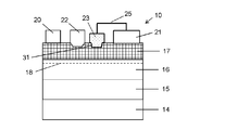
- FIG. 1 is a schematic cross-sectional view showing the semiconductor device of the first embodiment.
- the semiconductor device 10 shown in FIG. 1 includes a channel layer 16 and a barrier layer 17 made of a nitride-based semiconductor, and a two-dimensional electron gas layer 18 generated to extend in the vicinity of the interface between the channel layer 16 and the barrier layer 17 in plan view.
- the auxiliary film 23 is separated from the electrode (second electrode) 20 and formed in the recess 31 and made of a p-type nitride semiconductor.
- the auxiliary film 23 can be, for example, p-type GaN or Al (1-x) Ga x N (where x is 0 or more and 1 or less).
- the semiconductor device 10 can further include a substrate 14 and a buffer layer 15 made of a nitride-based semiconductor provided on the substrate 14.
- the formation of the two-dimensional electron gas layer 18 in the channel layer 16 can reduce the on-resistance of the semiconductor device 10.
- the substrate 14 can be, for example, a silicon substrate or a SiC substrate
- the channel layer 16 can be, for example, a GaN layer
- the barrier layer 17 can be, for example, an AlGaN layer.
- the barrier layer 17 may be the same material as the auxiliary film 23 or may be a different material from the auxiliary film 23.
- the buffer layer 15 can have, for example, a laminated structure of nitride-based semiconductor layers having different compositions.
- the drain electrode 21 and the auxiliary film 23 are electrically connected using the wiring 25.
- the wiring 25 may be the same material as the drain electrode 21 or the same material as the auxiliary film 23, or may be a different material from these.
- the drain electrode 21 and the auxiliary film 23 may be electrically connected without the wiring 25.
- the auxiliary film 23 may be formed on the surface of the barrier 17 between the recess 31 and the drain electrode 21, and the auxiliary film 23 may be in direct contact with the drain electrode 21. Since the auxiliary film 23 is also formed on the barrier layer 17 between the recess 31 and the drain electrode 21, the nitride semiconductor layer in the vicinity of the drain electrode (first electrode) 21 where electrons are relatively easily trapped. Electrons trapped in the region can be neutralized more effectively, and the current collapse phenomenon can be suppressed more effectively.
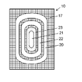
- the auxiliary film 23 is provided to surround the drain electrode 21.
- the auxiliary electrode (auxiliary film) 23 may be periodically spaced to surround the drain electrode 21 rather than completely surrounding the auxiliary electrode (auxiliary film) 23. desirable.
- the source electrode 20 is provided outside the drain electrode 21 in FIG. 4
- the drain electrode 21 may be provided outside the source electrode 20.
- the auxiliary film 23 is provided so as to surround the drain electrode 21 inside in a ring shape.
- the auxiliary film 23 is provided so as to surround the drain electrode 21, whereby the auxiliary film 23 having a larger area can be provided in the region adjacent to the drain electrode 21. This makes the current collapse phenomenon more efficient. Can be suppressed. Further, as in the semiconductor device of the third embodiment and its modification described later, the recess 31 provided with a part of the auxiliary film 23 is a drain electrode 21 in the region between the drain electrode 21 and the gate electrode 22. May be periodically provided at intervals in the direction in which the nitride semiconductor layer is stretched.
- the drain electrode (first electrode) 21 is applied with a higher potential than the source electrode (second electrode) 20.
- the drain electrode (first electrode) 21 and the source electrode (second electrode) 20 are provided on the barrier layer 17, but the channel layer 16 is penetrated through the barrier layer 17. It is possible to provide a groove portion reaching the above and to provide a drain electrode (first electrode) 21 and a source electrode (second electrode) 20 in the groove portion. Further, the drain electrode (first electrode) 21 and the source electrode (second electrode) 20 may be formed on a contact layer made of a nitride semiconductor further provided on the barrier layer.
- a gate electrode (control electrode) 22 for controlling a main current flowing between the drain electrode (first electrode) 21 and the source electrode (second electrode) 20 is further provided.
- the gate electrode 22 is also formed in a recess formed on the upper surface of the barrier layer 17. Since the recess is formed on the upper surface of the barrier layer 17, the carrier concentration of the two-dimensional electron gas layer 18 immediately below the gate electrode 22 is reduced, the current path is blocked, and the semiconductor device 10 becomes a normally-off device.
- the depth of the recess of the barrier layer under the gate electrode 22 may be the same as that of the recess 31. Further, as in the semiconductor device of FIG. 3, the recess may not be formed in the region of the barrier layer 17 under the gate electrode 22.
- the recess 31 and the auxiliary film 23 are formed between the drain electrode (first electrode) 21 and the gate electrode (control electrode) 22, and the auxiliary film 23 is separated from the gate electrode (control electrode) 22. preferable. By separating the auxiliary film 23 from the gate electrode (control electrode) 22 in this manner, it is possible to reduce the leak current between the auxiliary film 23 and the gate electrode (control control electrode) 22.
- the auxiliary film 23 formed in the recess 31 more effectively mediums the electrons trapped in the nitride-based semiconductor layer which causes the current collapse. Sum and current collapse can be suppressed more effectively. Further, by forming the auxiliary film 23 in the recess 31, an increase in on-resistance can be suppressed.
- the barrier layer 17 is formed on the channel layer 16 by a known method (for example, metal organic chemical vapor deposition).
- a photoresist film 24 is formed on the barrier layer 17 in a region other than the auxiliary film formation region 29 and the gate formation region 30 by a known method (for example, a photolithography method).
- a known method for example, a photolithography method.
- recesses in the gate formation region 30 and the auxiliary film formation region 29 are formed on the surface of the barrier layer 17.
- the photoresist film 24 is removed, and a p-type nitride semiconductor is formed, for example, by metal organic vapor phase epitaxy. Thereafter, the p-type nitride semiconductor on the formation region of the source electrode 20 and the periphery thereof, the p-type nitride semiconductor on the formation region of the drain electrode 21, on the space between the gate formation region 30 and the recess 31 The p-type nitride semiconductor is removed.
- the p-type nitride semiconductor film 22 is formed on the recess of the gate formation region 30, and the p-type nitride semiconductor film 23 is formed on the recess 31. Note that an electrode may be formed on the p-type nitride semiconductor film 22 in a later step to form the gate electrode 22.
- the drain electrode (drain ohmic electrode) 21 and the source electrode (source ohmic electrode) 20 are formed.
- the substrate 14 and the buffer layer 15 below the channel layer 16 are omitted.
- a wiring 25 for electrically connecting the p-type nitride semiconductor film 23 and the drain electrode 21 is formed.
- the semiconductor device 10 of the first embodiment shown in FIG. 1 can be manufactured. As described above with reference to FIG. 2, in the semiconductor device 10, since the auxiliary film 23 is formed in the recess, the leak current can be easily reduced, and the current collapse phenomenon can be more effectively suppressed. .
- FIG. 5 is a schematic cross-sectional view showing the semiconductor device of the second embodiment.
- the semiconductor device 13 of FIG. 5 has substantially the same structure as the semiconductor device of the third embodiment shown in FIG. 4 except that a part of the drain electrode 21 is provided on the upper surface of the auxiliary film 23. It differs from the semiconductor device of one embodiment. Also in the semiconductor device of the second embodiment, the same effect as that of the semiconductor device of the first embodiment can be obtained. As shown in FIG. 5, the end of the auxiliary film 23 on the source electrode 20 side may be closer to the source electrode 20 than the end of the drain electrode 21 on the source electrode 20 side.
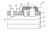
- FIG. 6 (a) is a schematic cross-sectional view showing the semiconductor device of the third embodiment
- FIG. 6 (b) is a top view of FIG. 6 (a).
- 6B shows the upper surface of the region in the vicinity of the drain electrode 21, and an insulating film 32 described later and part of the drain electrode 21 provided on the insulating film 32 are omitted.
- the insulating film 32 is provided on the auxiliary film 23 and the drain electrode 21, and a part of the drain electrode 21 is also provided on the insulating film 32.
- the insulating film 32 can be, for example, a SiO 2 film or a SiN film.
- the shape seen from above the recess 31 in which a part of the auxiliary film 23 is provided is circular, and the recess 31 in which a part of the auxiliary film 23 is provided is In the region between the drain electrode 21 and the gate electrode 22, the drain electrode 21 is periodically provided at intervals in the direction in which the nitride semiconductor layer is stretched (see FIG. 6B). Also in the semiconductor device of the third embodiment, the same effects as those of the semiconductor devices of the first and second embodiments can be obtained.
- the semiconductor device of the third embodiment by providing a part of the auxiliary film 23 in the recess 31, hole injection efficiency can be increased in the region of the recess 31, and the region between the recess 31 and the recess 31 is provided. Then, since the thickness of the barrier layer 17 does not decrease, it is possible to suppress the decrease in the concentration of the two-dimensional electric gas layer 18 and to suppress the increase in the on-resistance of the FET.
- Recesses 31 in which a part of the auxiliary film 23 is provided are periodically provided at intervals in a direction (for example, perpendicular direction) intersecting the direction connecting the drain electrode 21 and the source electrode 20. The portion where the recess 31 is provided can effectively inject holes.
- the thickness of a barrier layer does not become thin in the part in which the recessed part 31 is not provided, an electric current can be flowed favorably. Therefore, the increase in the on-resistance of the semiconductor device can be reduced while suppressing the current collapse.
- the dimension X of the recess 31 along the drain electrode 21 smaller than the dimension Y between the recesses 31 along the drain electrode 21, the hole injection effect is enhanced, and the current collapse can be further improved.
- the ON in the reduction of the carrier concentration of the two-dimensional electron gas layer by providing the recess The current collapse can be improved while suppressing the increase in resistance.
- the recess 31 and the auxiliary film 23 are formed only on one side of the drain electrode 21 when viewed from the top view of FIG. 6B, the recess 31 and the auxiliary film 23 surround the drain electrode 31. It may be formed.
- FIG. 7 is a schematic cross-sectional view showing a first modified example of the semiconductor device of the third embodiment.
- the recess 31 in which a part of the auxiliary film 23 is provided is formed deeper than the recess of the barrier layer 17 directly below the gate electrode 22, and the recess 31 penetrates the barrier layer 17.
- Channel layer 16 Also in the first modification of the semiconductor device of the third embodiment, the same effect as that of the semiconductor device of the third embodiment can be obtained.
- FIG. 8 is a top view showing a second modification of the semiconductor device of the third embodiment.
- FIG. 8 shows the upper surface of the region in the vicinity of the drain electrode 21 similarly to FIG. 6B, and the insulating film 32 and part of the drain electrode 21 provided on the insulating film 32 are omitted.
- the shape seen from above the recess 31 in which a portion of the auxiliary film 23 is provided is rectangular, and the recess 31 in which a portion of the auxiliary film 23 is provided is a drain electrode. I am in contact with 21.
- the shape seen from the upper part of the recessed part 31 can also be made into various shapes, such as a circle
- the recess 31 in which a part of the auxiliary film 23 is provided is in contact with the drain electrode 21, even in the nitride semiconductor layer near the drain electrode 21 where electrons are easily trapped, Hole injection can be made more effective, and current collapse can be reduced.
- the recess 31 and the auxiliary film 23 are formed only on one side of the drain electrode 21 when viewed from the top view of FIG. 8, the recess 31 and the auxiliary film 23 are formed to surround the drain electrode 31. It is good.
- FIG. 9 is a top view showing a third modification of the semiconductor device of the third embodiment. Similarly to FIG. 6B, FIG. 9 also shows the top surface of the region in the vicinity of the drain electrode 21. The insulating film 32 and part of the drain electrode 21 provided on the insulating film 32 are omitted.
- the semiconductor device shown in FIG. 9 has substantially the same configuration as the semiconductor device shown in FIG. 8, but an auxiliary film 23 is provided over the entire region of the barrier layer sandwiched between the recess 31 and the adjacent recess 31. The difference is that the auxiliary film 23 is provided on the recess 31 and the periphery thereof, and the auxiliary film 23 is periodically provided at intervals. In the semiconductor device of FIG.
- the recess 31 and the auxiliary film 23 are periodically provided in the region between the drain electrode 21 and the gate electrode 22 in the direction in which the drain electrode 21 extends on the nitride semiconductor layer. Since the concave portions 31 provided between the adjacent auxiliary films 23 and the region where the auxiliary film 23 is not provided can flow a current well. Therefore, the increase in the on resistance of the semiconductor device can be reduced.
- FIG. 10 is a top view showing a fourth modification of the semiconductor device of the third embodiment. Similarly to FIG. 6B, FIG. 10 also shows the upper surface of the region in the vicinity of the drain electrode 21. The insulating film 32 and part of the drain electrode 21 provided on the insulating film 32 are omitted.
- the shape seen from above the recess 31 in which a part of the auxiliary film 23 is provided is rectangular, and the auxiliary film 23 is provided in the recess 31.
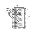
- the recess 31 is provided between the drain electrode 21 and the source electrode 20 so as to be separated from the drain electrode 21, and the end 23 B of the auxiliary film 23 on the barrier layer between the adjacent recesses 31 is the periphery of the recess 31.
- the end of the auxiliary film 23 on the barrier layer is closer to the drain electrode 21 than the end 23A, and the shape seen from above the auxiliary film 23 is a comb shape. Also in the semiconductor device of FIG. 10, the same effect as that of the semiconductor device of the second embodiment can be obtained. Although the recess 31 and the auxiliary film 23 are formed only on one side of the drain electrode 21 when viewed from the top view of FIG. 10, the recess 31 and the auxiliary film 23 are formed so as to surround the drain electrode 31. It is good.
- FIG. 11A is a schematic cross-sectional view showing a semiconductor device 41 of the fourth embodiment
- FIG. 11B is a top view of FIG. FIG. 11B shows the upper surface of the region in the vicinity of the drain electrode 21, and the insulating film 32 and the wiring 25 on the insulating film 32 are omitted.
- the auxiliary film 23 and the drain electrode 21 are electrically connected by the wiring 25.
- the auxiliary film 23 and the drain electrode 21 are connected to the wiring 25 through the opening provided in the insulating film 32 (see FIG. 11A).
- the recess 31 in which a part of the auxiliary film 23 is provided does not penetrate the barrier layer 17 and does not reach the channel layer 16.
- the recess 31 partially provided may penetrate through the barrier layer 17 to reach the channel layer 16.
- the same effect as that of the semiconductor device of the fourth embodiment can be obtained.
- the present invention is not limited to the above embodiment.
- the above embodiment is an exemplification, and it has substantially the same configuration as the technical idea described in the claims of the present invention, and any one having the same function and effect can be used. It is included in the technical scope of the invention.
- Buffer layer 16 Channel layer (first nitride-based semiconductor layer) 17: Barrier layer (second nitride semiconductor layer) 18: Two-dimensional electron gas layer 20: Source electrode (second electrode) 21 ... drain electrode (first electrode) 22: Gate electrode (control electrode) 23 ... Auxiliary film (auxiliary electrode) 24 Photoresist film 25 Wiring 29 Auxiliary electrode formation region 30 Gate formation region 31 Concave portion 32 Insulating film
Landscapes
- Junction Field-Effect Transistors (AREA)
Abstract
半導体装置は、第1の窒化物系半導体層と、前記第1の窒化物系半導体層上の第2の窒化物系半導体層と、前記第1の窒化物系半導体層と前記第2の窒化物系半導体層との界面近傍の2次元電子ガス層と、前記2次元電子ガス層と電気的に接続する第1の電極と、前記2次元電子ガス層と電気的に接続する第2の電極と、前記第1の電極と前記第2の電極との間にあって、前記第2の窒化物系半導体層の表面に設けられた凹部と、前記第1の電極と電気的に接続し、前記第2の電極とは離間し、前記凹部内に設けられたp型窒化物半導体から成る補助膜とを備える。これにより、電流コラプスを抑制するとともに、オン抵抗の上昇を抑制することができる。
Description
本発明は、半導体装置及びその製造方法に関する。
窒化ガリウム(GaN)に代表されるIII-V族窒化物系化合物半導体、いわゆる窒化物半導体が注目を集めている。窒化物半導体は、一般式がInxGayAl1-x-yN(0≦x≦1、0≦y≦1、x+y≦1)で表される、III族元素であるアルミニウム(Al)、ガリウム(Ga)及びインジウム(In)と、V族元素である窒素(N)とからなる化合物半導体である。窒化物半導体は種々の混晶を形成することができ、ヘテロ接合界面を容易に形成することができる。窒化物半導体のヘテロ接合には、ドーピングなしの状態においても自発分極又はピエゾ分極によって高濃度の2次元電子ガス層が接合界面に発生するという特徴がある。この高濃度の2次元電子ガス層をキャリアとして用いた電界効果トランジスタ(FET:Field Effect Transistor)が、高周波用及び大電力用のデバイスとして注目を集めている。
しかしながら、窒化物半導体を用いたFETには電流コラプスと呼ばれる現象が生じやすい。電流コラプスとは、一旦デバイスをオフ状態とした後、再びオン状態とする際に電流が一定時間流れにくくなる現象である。電流コラプスの特性が悪いと高速なスイッチングが困難となり、デバイスの動作に極めて深刻な問題が生じる。
特許文献1では、FETのドレイン電極近傍にp型窒化物半導体層(例えば、p型GaN層)を設け、p型窒化物半導体層とドレイン電極を電気的に接続し、p型窒化物半導体層からホールを注入することで、電流コラプスの原因となる半導体層中にトラップされた電子を中和し、電流コラプスを抑制している。
しかしながら、特許文献1のFETでは、p型窒化物半導体層をバリア層(電子供給層)上に部分的に形成するため、ホールの注入効率が悪いという問題があった。また、ホールの注入効率を上げるためにバリア層を薄くすると、2次元電子ガス層のキャリア濃度が低下し、オン抵抗が増加するという問題があった。
本発明は、上記問題点に鑑みてなされたものであって、電流コラプスを抑制するとともに、オン抵抗の上昇を抑制することができる半導体装置及びその製造方法を提供することを目的とする。
上記目的を達成するために、本発明は、窒化物系半導体層と、前記窒化物系半導体層と接する第1の電極と、前記窒化物系半導体層と接する第2の電極と、前記第1の電極と前記第2の電極との間の前記窒化物系半導体層に形成された凹部と、前記第1の電極と電気的に接続し、前記第2の電極とは離間し、前記凹部内に設けられ、p型窒化物半導体から成る補助膜とを備えたものであることを特徴とする半導体装置を提供する。
このように、第1の電極と第2の電極との間の窒化物系半導体層に形成された凹部内にp型窒化物半導体の補助膜を第1の電極と電気的に接続することで、補助膜からホールが注入され、電流コラプスの原因となる窒化物系半導体層にトラップされた電子をより効果的に中和することができ、電流コラプスをより効果的に抑制することができる。また、このように、凹部内にp型窒化物半導体を設けることによって、オン抵抗の増加を抑制することができる。
上記目的を達成するために、本発明の製造方法は、窒化物系半導体層と接する第1の電極及び第2の電極を形成する工程と、前記窒化物系半導体層上に凹部を形成する工程と、前記凹部内にp型の窒化物半導体から成る補助膜を形成する工程と、前記第1の電極と電気的に接続する配線を形成する工程とを特徴とする半導体装置の製造方法を提供する。
本発明の半導体装置の製造方法によれば、第1の電極と電気的に接続したp型の窒化物半導体の補助膜を凹部内に形成することで、凹部内に形成されたp型の窒化物半導体からホールが注入され、電流コラプスの原因となる窒化物系半導体層にトラップされた電子をより効果的に中和し、電流コラプスをより効果的に抑制することができる。また、このように、凹部内にp型の窒化物半導体を設けることにより、容易にオン抵抗の増加を抑制することができる。
以上のように、本発明の半導体装置及びその製造方法によれば、ドレイン電極と電気的に接続するp型窒化物半導体を第1の電極と第2の電極との間に凹部内に形成することで、p型金属酸化物半導体からホール注入することで電流コラプスの原因となる窒化物系半導体層にトラップされた電子をより効果的に中和し、電流コラプスをより効果的に抑制し、オン抵抗の増加を抑制することができる。
以下、本発明について、実施態様の一例として、図を参照しながら詳細に説明するが、本発明はこれに限定されるものではない。
まず、第1実施形態の半導体装置について、図1を参照しながら説明する。
図1は第1実施形態の半導体装置を示す概略断面図である。図1の半導体装置10は、窒化物系半導体からなるチャネル層16及びバリア層17と、チャネル層16及びバリア層17との界面近傍に平面的に広がるように生じる2次元電子ガス層18と、2次元電子ガス層18と電気的に接続するドレイン電極(第1の電極)21と、2次元電子ガス層18と電気的に接続するソース電極(第2の電極)20と、ドレイン電極(第1の電極)21とソース電極(第2の電極)20との間に設けられた窒化物系半導体表面上の凹部31と、ドレイン電極(第1の電極)21と電気的に接続し、ソース電極(第2の電極)20とは離間し、凹部31内に形成されたp型窒化物半導体から成る補助膜23とを備えている。補助膜23は、例えば、p型のGaN又はAl(1-x)GaxN(但しxは0以上1以下)とすることができる。
ここで、半導体装置10は、さらに、基板14と、基板14上に設けられた窒化物系半導体からバッファ層15とを有することができる。チャネル層16内に2次元電子ガス層18が形成されていることで、半導体装置10のオン抵抗を低減させることができる。
基板14は、例えば、シリコン基板又はSiC基板とすることができ、チャネル層16は、例えば、GaN層とすることができ、バリア層17は、例えば、AlGaN層とすることができる。バリア層17は、補助膜23と同じ材料であってもよいし、補助膜23と異なる材料であってもよい。
また、バッファ層15は、例えば、組成の異なる窒化物系半導体層の積層構造とすることができる。
また、バッファ層15は、例えば、組成の異なる窒化物系半導体層の積層構造とすることができる。
第1実施形態の半導体装置10では、ドレイン電極21と補助膜23とを配線25を用いて電気的に接続している。配線25はドレイン電極21と同じ材料又は補助膜23と同じ材料であってもよいし、これらと異なる材料であってもよい。
また、配線25を介さずドレイン電極21と補助膜23とが電気的に接続していても良い。例えば、図3のように、補助膜23が凹部31とドレイン電極21との間のバリア17の表面上にも形成され、補助膜23がドレイン電極21と直接接触していても良い。補助膜23が凹部31とドレイン電極21との間のバリア層17上にも形成しているので、電子が比較的トラップされ易いドレイン電極(第1の電極)21の近傍の窒化物半導体層の領域においてトラップされた電子を、より効果的に中和することができ、電流コラプス現象をより効果的に抑制することができる。
また、半導体装置10を上方から平面的に見て、図4で示すように、補助膜23がドレイン電極21の周りを取り囲むように設けられている。ここで、補助電極(補助膜)23が周りを取り囲むとは完全に囲むよりも、補助電極(補助膜)23が周期的に間隔を開けてドレイン電極21の周りを取り囲むように配置することが望ましい。これにより、ドレイン電極(第1の電極)21の近傍の窒化物半導体層の領域においてトラップされた電子を、より効果的に中和することができ、電流コラプス現象をより効果的に抑制することができる。
また、図4において、ソース電極20がドレイン電極21よりも外側に設けられているが、ドレイン電極21がソース電極20よりも外側に設けられていても良い。この場合、補助膜23はドレイン電極21よりも内側でリング状に囲むように設けられることは言うまでもない。補助膜23がドレイン電極21を取り囲むように設けられていることで、ドレイン電極21に隣接した領域に、より広い面積の補助膜23を設けることができ、これにより、より効率的に電流コラプス現象を抑制することができる。また、後述する第3の実施形態やその変形例の半導体装置のように、補助膜23の一部が設けられている凹部31はドレイン電極21とゲート電極22との間の領域においてドレイン電極21が窒化物半導体層上を延伸する方向に間隔をあけて周期的に設けられていても良い。
また、図4において、ソース電極20がドレイン電極21よりも外側に設けられているが、ドレイン電極21がソース電極20よりも外側に設けられていても良い。この場合、補助膜23はドレイン電極21よりも内側でリング状に囲むように設けられることは言うまでもない。補助膜23がドレイン電極21を取り囲むように設けられていることで、ドレイン電極21に隣接した領域に、より広い面積の補助膜23を設けることができ、これにより、より効率的に電流コラプス現象を抑制することができる。また、後述する第3の実施形態やその変形例の半導体装置のように、補助膜23の一部が設けられている凹部31はドレイン電極21とゲート電極22との間の領域においてドレイン電極21が窒化物半導体層上を延伸する方向に間隔をあけて周期的に設けられていても良い。
ドレイン電極(第1の電極)21は、ソース電極(第2の電極)20よりも高電位が印加される。第1実施形態の半導体装置10では、ドレイン電極(第1の電極)21とソース電極(第2の電極)20はバリア層17上に設けているが、バリア層17を貫通してチャネル層16に達する溝部を設けて、溝部内にドレイン電極(第1の電極)21とソース電極(第2の電極)20を設けても良い。また、ドレイン電極(第1の電極)21とソース電極(第2の電極)20はバリア層上に更に設けた窒化物半導体から成るコンタクト層上に形成されても良い。
ドレイン電極(第1の電極)21とソース電極(第2の電極)20との間を流れる主電流を制御するゲート電極(制御電極)22を更に備える。図1の半導体装置のように、ゲート電極22はバリア層17の上面にリセスが形成された中にも形成されている。バリア層17の上面にリセスが形成されていることにより、ゲート電極22直下の2次元電子ガス層18のキャリア濃度が減少し、電流通路が遮断され、半導体装置10はノーマリオフデバイスとなる。なお、ゲート電極22下のバリア層のリセスの深さは凹部31と同じ深さとしても良い。また、図3の半導体装置のように、ゲート電極22下のバリア層17の領域はリセスを形成しなくても良い。
凹部31及び補助膜23はドレイン電極(第1の電極)21とゲート電極(制御電極)22との間に形成され、補助膜23はゲート電極(制御電極)22から離間したものであることが好ましい。このように補助膜23がゲート電極(制御電極)22から離間していることで、補助膜23とゲート電極(制御制御電)22との間のリーク電流を低減することができる。
凹部31及び補助膜23はドレイン電極(第1の電極)21とゲート電極(制御電極)22との間に形成され、補助膜23はゲート電極(制御電極)22から離間したものであることが好ましい。このように補助膜23がゲート電極(制御電極)22から離間していることで、補助膜23とゲート電極(制御制御電)22との間のリーク電流を低減することができる。
上記で説明した第1実施形態の半導体装置によれば、凹部31内に形成された補助膜23が、電流コラプスの原因となる窒化物系半導体層内部にトラップされた電子をより効果的に中和し、電流コラプスをより効果的に抑制することができる。また、補助膜23を凹部31内に形成することで、オン抵抗の増加を抑制することができる。
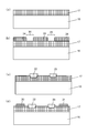
ここで、第1実施形態の半導体装置の製造方法を示す工程フローを説明する。
まず、図2(a)に示すように、既知の方法(例えば、有機金属気相成長法)により、チャネル層16上にバリア層17を形成する。次に、図2(b)に示すように、バリア層17上に既知の方法(例えば、フォトリソグラフィー法)により、補助膜形成領域29及びゲート形成領域30以外の領域に、フォトレジスト膜24を形成する。
次に、図2(c)に示すように、バリア層17の表面にゲート形成領域30内と補助膜形成領域29内の凹部を形成する。そして、フォトレジスト膜24を除去し、例えば、有機金属気相成長法にてp型の窒化物半導体を形成する。その後にソース電極20の形成領域とその周囲の上のp型の窒化物半導体、ドレイン電極21の形成領域の上のp型の窒化物半導体、ゲート形成領域30内と凹部31との間の上のp型の窒化物半導体を除去する。これにより、p型窒化物半導体膜22がゲート形成領域30の凹部上に形成され、p型窒化物半導体膜23が凹部31上に形成される。なお、後工程でp型窒化物半導体膜22上に電極を形成してゲート電極22としても良い。
まず、図2(a)に示すように、既知の方法(例えば、有機金属気相成長法)により、チャネル層16上にバリア層17を形成する。次に、図2(b)に示すように、バリア層17上に既知の方法(例えば、フォトリソグラフィー法)により、補助膜形成領域29及びゲート形成領域30以外の領域に、フォトレジスト膜24を形成する。
次に、図2(c)に示すように、バリア層17の表面にゲート形成領域30内と補助膜形成領域29内の凹部を形成する。そして、フォトレジスト膜24を除去し、例えば、有機金属気相成長法にてp型の窒化物半導体を形成する。その後にソース電極20の形成領域とその周囲の上のp型の窒化物半導体、ドレイン電極21の形成領域の上のp型の窒化物半導体、ゲート形成領域30内と凹部31との間の上のp型の窒化物半導体を除去する。これにより、p型窒化物半導体膜22がゲート形成領域30の凹部上に形成され、p型窒化物半導体膜23が凹部31上に形成される。なお、後工程でp型窒化物半導体膜22上に電極を形成してゲート電極22としても良い。
次に、図2(d)に示すように、ドレイン電極(ドレインオーミック電極)21及びソース電極(ソースオーミック電極)20を形成する。なお、図2において、チャネル層16より下層の基板14及びバッファ層15は省略されている。その後、p型窒化物半導体膜23とドレイン電極21とを電気的に接続する配線25を形成する。
上記のようにして、図1に示す第1実施形態の半導体装置10を製造することができる。
上記で図2を用いて説明したように、半導体装置10では補助膜23が凹部内に形成されているので、容易にリーク電流を低下させることができ、電流コラプス現象をより効果的に抑制できる。
上記で図2を用いて説明したように、半導体装置10では補助膜23が凹部内に形成されているので、容易にリーク電流を低下させることができ、電流コラプス現象をより効果的に抑制できる。
次に、第2実施形態の半導体装置について、図5を参照しながら説明する。
図5は第2実施形態の半導体装置を示す概略断面図である。図5の半導体装置13は、図4に示す第3実施形態の半導体装置とほぼ同様の構成であるが、ドレイン電極21の一部が補助膜23の上面上に設けられている点で、第1実施形態の半導体装置と異なっている。第2実施形態の半導体装置においても、第1実施形態の半導体装置と同様の効果を得ることができる。図5で示すように、ソース電極20側の補助膜23の端はソース電極20側のドレイン電極21の端よりもソース電極20側としても良い。
次に、第3実施形態の半導体装置について、図6-10を参照しながら、説明する。
図6(a)は第3実施形態の半導体装置を示す概略断面図であり、図6(b)は図6(a)の上面図である。なお、図6(b)はドレイン電極21近傍の領域の上面を示すものであり、また、後述する絶縁膜32、及び絶縁膜32上に設けられたドレイン電極21の一部は省略されている。
図6の半導体装置40は、補助膜23及びドレイン電極21上に絶縁膜32が設けられ、ドレイン電極21の一部が絶縁膜32上にも設けられている。ここで、絶縁膜32は、例えば、SiO2膜、又はSiN膜とすることができる。なお、図6の半導体装置40において、補助膜23の一部が設けられている凹部31の上から見た形状は円形であり、また、補助膜23の一部が設けられている凹部31はドレイン電極21とゲート電極22との間の領域においてドレイン電極21が窒化物半導体層上を延伸する方向に間隔をあけて周期的に設けられている(図6(b)参照)。第3実施形態の半導体装置においても、第1及び第2実施形態の半導体装置と同様の効果を得ることができる。
図6の半導体装置40は、補助膜23及びドレイン電極21上に絶縁膜32が設けられ、ドレイン電極21の一部が絶縁膜32上にも設けられている。ここで、絶縁膜32は、例えば、SiO2膜、又はSiN膜とすることができる。なお、図6の半導体装置40において、補助膜23の一部が設けられている凹部31の上から見た形状は円形であり、また、補助膜23の一部が設けられている凹部31はドレイン電極21とゲート電極22との間の領域においてドレイン電極21が窒化物半導体層上を延伸する方向に間隔をあけて周期的に設けられている(図6(b)参照)。第3実施形態の半導体装置においても、第1及び第2実施形態の半導体装置と同様の効果を得ることができる。
第3実施形態の半導体装置においては、補助膜23の一部を凹部31内に設けることで、凹部31の領域ではホール注入効率を上げることができるとともに、凹部31と凹部31との間の領域では、バリア層17の厚さが薄くならないので、2次元電ガス層18の濃度が低下することを抑制し、FETのオン抵抗の増加を抑制させることができる。補助膜23の一部が設けられている凹部31がドレイン電極21とソース電極20とを結ぶ方向とは交わる方向(例えば垂直な方向)に間隔をあけて周期的に設けられている。凹部31が設けられている部分は効果的にホールを注入することができる。そして凹部31が設けられていない部分はバリア層の厚みが薄くならないので、良好に電流を流すことができる。それゆえ、電流コラプスを抑制しつつ、半導体装置のオン抵抗が増加することを低減することができる。ここで、ドレイン電極21に沿った凹部31の寸法Xをドレイン電極21に沿った凹部31間の寸法Yよりも小さくすることで、ホール注入効果が高まり、より電流コラプスを改善することができる。一方、ドレイン電極21に沿った凹部31の寸法Xをドレイン電極21に沿った凹部31間の寸法Yよりも大きくすることで、凹部を設けることによる2次元電子ガス層のキャリア濃度の低下におけるオン抵抗の増加を抑制しつつ、電流コラプスを改善することができる。
なお、図6(b)の上面図から見て、凹部31及び補助膜23はドレイン電極21の一方の側にしか形成していないが、凹部31及び補助膜23はドレイン電極31を取り囲むように形成されていても良い。
なお、図6(b)の上面図から見て、凹部31及び補助膜23はドレイン電極21の一方の側にしか形成していないが、凹部31及び補助膜23はドレイン電極31を取り囲むように形成されていても良い。
図7は第3実施形態の半導体装置の第1の変形例を示す概略断面図である。図7の半導体装置40’では、補助膜23の一部が設けられている凹部31がゲート電極22直下のバリア層17のリセスよりも深く形成されており、凹部31がバリア層17を貫通してチャネル層16に達している。第3実施形態の半導体装置の第1の変形例においても、第3実施形態の半導体装置と同様の効果を得ることができる。
図8は第3実施形態の半導体装置の第2の変形例を示す上面図である。図8は図6(b)と同様にドレイン電極21近傍の領域の上面を示すものであり、絶縁膜32、及び絶縁膜32上に設けられたドレイン電極21の一部は省略されている。図8の半導体装置においては、補助膜23の一部が設けられている凹部31の上から見た形状は長方形であり、また、補助膜23の一部が設けられている凹部31はドレイン電極21と接している。
なお、凹部31の上から見た形状は、例えば、円、六角形等様々な形状とすることもできる。
図8の半導体装置においては、補助膜23の一部が設けられている凹部31がドレイン電極21と接しているので、電子がトラップしやすいドレイン電極21近傍の窒化物系半導体層内においても、より効果的にホール注入させることができ、電流コラプスを低減することができる。なお、図8の上面図から見て、凹部31及び補助膜23はドレイン電極21の一方の側にしか形成していないが、凹部31及び補助膜23はドレイン電極31を取り囲むように形成されていても良い。
なお、凹部31の上から見た形状は、例えば、円、六角形等様々な形状とすることもできる。
図8の半導体装置においては、補助膜23の一部が設けられている凹部31がドレイン電極21と接しているので、電子がトラップしやすいドレイン電極21近傍の窒化物系半導体層内においても、より効果的にホール注入させることができ、電流コラプスを低減することができる。なお、図8の上面図から見て、凹部31及び補助膜23はドレイン電極21の一方の側にしか形成していないが、凹部31及び補助膜23はドレイン電極31を取り囲むように形成されていても良い。
図9は第3実施形態の半導体装置の第3の変形例を示す上面図である。図9も図6(b)と同様にドレイン電極21近傍の領域の上面を示すものであり、絶縁膜32、及び絶縁膜32上に設けられたドレイン電極21の一部は省略されている。図9の半導体装置は、図8の半導体装置とほぼ同様の構成であるが、凹部31と隣の凹部31との間で挟まれたバリア層の領域上の全域に亘って補助膜23が設けられている訳では無く、補助膜23が凹部31とその周囲に設けられ、補助膜23が間隔をあけて周期的に設けられている点で異なっている。
図9の半導体装置においては、ドレイン電極21とゲート電極22との間の領域で凹部31及び補助膜23はドレイン電極21が窒化物半導体層上を延伸する方向に間隔をあけて周期的に設けられているので、隣り合う補助膜23間に設けられた凹部31及び補助膜23が設けられていない領域は良好に電流を流すことができる。それゆえ、半導体装置のオン抵抗の増加を低減することができる。
図9の半導体装置においては、ドレイン電極21とゲート電極22との間の領域で凹部31及び補助膜23はドレイン電極21が窒化物半導体層上を延伸する方向に間隔をあけて周期的に設けられているので、隣り合う補助膜23間に設けられた凹部31及び補助膜23が設けられていない領域は良好に電流を流すことができる。それゆえ、半導体装置のオン抵抗の増加を低減することができる。
図10は第3実施形態の半導体装置の第4の変形例を示す上面図である。図10も図6(b)と同様にドレイン電極21近傍の領域の上面を示すものであり、絶縁膜32、及び絶縁膜32上に設けられたドレイン電極21の一部は省略されている。図10の半導体装置においては、補助膜23の一部が設けられている凹部31の上から見た形状は長方形であり、凹部31内に補助膜23が設けられている。また、凹部31はドレイン電極21から離間してドレイン電極21とソース電極20との間に設けられており、隣り合う凹部31間のバリア層上の補助膜23の端23Bは凹部31の周囲のバリア層上の補助膜23の端23Aよりもドレイン電極21側であり、補助膜23の上から見た形状は櫛型状である。
図10の半導体装置においても第2実施形態の半導体装置と同様の効果を得ることができる。また、図10の上面図から見て、凹部31及び補助膜23はドレイン電極21の一方の側にしか形成していないが、凹部31及び補助膜23はドレイン電極31を取り囲むように形成されていても良い。
図10の半導体装置においても第2実施形態の半導体装置と同様の効果を得ることができる。また、図10の上面図から見て、凹部31及び補助膜23はドレイン電極21の一方の側にしか形成していないが、凹部31及び補助膜23はドレイン電極31を取り囲むように形成されていても良い。
次に、第4実施形態の半導体装置41について、図11を参照しながら、説明する。
図11(a)は第4実施形態の半導体装置41を示す概略断面図であり、図11(b)は図11(a)の上面図である。なお、図11(b)はドレイン電極21近傍の領域の上面を示すものであり、また、絶縁膜32、及び絶縁膜32上の配線25は省略されている。図11の半導体装置41は補助膜23とドレイン電極21は配線25によって電気的に接続されている。ここで、補助膜23及びドレイン電極21は絶縁膜32に設けられた開口部を介して配線25に接続されている(図11(a)参照)。なお、図11の半導体装置41では、補助膜23の一部が設けられている凹部31がバリア層17を貫通せずにチャネル層16に達していない構成になっているが、補助膜23の一部が設けられている凹部31がバリア層17を貫通してチャネル層16に達する構成としてもよい。第5実施形態の半導体装置においても、第4実施形態の半導体装置と同様の効果を得ることができる。
なお、本発明は、上記実施形態に限定されるものではない。上記実施形態は、例示であり、本発明の特許請求の範囲に記載された技術的思想と実質的に同一な構成を有し、同様な作用効果を奏するものは、いかなるものであっても本発明の技術的範囲に包含される。
10、13、40、40’、41…半導体装置
14…基板、
15…バッファ層
16…チャネル層(第1の窒化物系半導体層)
17…バリア層(第2の窒化物系半導体層)
18…2次元電子ガス層
20…ソース電極(第2の電極)
21…ドレイン電極(第1の電極)
22…ゲート電極(制御電極)
23…補助膜(補助電極)
24…フォトレジスト膜
25…配線
29…補助電極形成領域
30…ゲート形成領域
31…凹部
32…絶縁膜
14…基板、
15…バッファ層
16…チャネル層(第1の窒化物系半導体層)
17…バリア層(第2の窒化物系半導体層)
18…2次元電子ガス層
20…ソース電極(第2の電極)
21…ドレイン電極(第1の電極)
22…ゲート電極(制御電極)
23…補助膜(補助電極)
24…フォトレジスト膜
25…配線
29…補助電極形成領域
30…ゲート形成領域
31…凹部
32…絶縁膜
Claims (9)
- 第1の窒化物系半導体層と、
前記第1の窒化物系半導体層上の第2の窒化物系半導体層と、
前記第1の窒化物系半導体層と前記第2の窒化物系半導体層との界面近傍の2次元電子ガス層と、
前記2次元電子ガス層と電気的に接続する第1の電極と、
前記2次元電子ガス層と電気的に接続する第2の電極と、
前記第1の電極と前記第2の電極との間にあって、前記第2の窒化物系半導体層の表面に設けられた凹部と、
前記第1の電極と電気的に接続し、前記第2の電極とは離間し、前記凹部内に設けられたp型窒化物半導体から成る補助膜と
を備えたものであることを特徴とする半導体装置。 - 前記第1の電極は前記第2の電極よりも高電位となる電極であることを特徴とする請求項1に記載の半導体装置。
- 前記凹部は前記第1の電極の延伸する方向に周期的に離間して配置されていることを特徴とする請求項1又は請求項2に記載の半導体装置。
- 前記凹部は前記第1の電極から離間し、
前記補助膜は前記凹部と前記第1の電極との間の前記第2の窒化物系半導体層上に形成されていることを特徴とする請求項1から請求項3のいずれか1項に記載の半導体装置。 - 前記凹部は前記第1の電極と接し、
前記補助膜は前記第1の電極と接触していることを特徴とする請求項1から請求項3のいずれか1項に記載の半導体装置。 - 前記凹部は前記第1の電極に沿って複数形成されていることを特徴とする請求項1から請求項5のいずれか1項に記載の半導体装置。
- 前記補助膜は前記第1の電極の周りを取り囲むように設けられたものであることを特徴とする請求項1から請求項6のいずれか1項に記載の半導体装置。
- 第1の窒化物系半導体層と、前記第1の窒化物系半導体層上に第2の窒化物系半導体層とを形成し、第1の窒化物系半導体層と第2の窒化物系半導体層との界面近傍に2次元電子ガス層を生じさせる工程と、
前記第2の窒化物系半導体層の表面に凹部を形成する工程と、
前記2次元電子ガス層に電気的に接続する第1の電極及び第2の電極を形成する工程と、
前記第1の電極と電気的に接続し、前記凹部内にp型の窒化物半導体層を形成する工程と
を備えることを特徴とする半導体装置の製造方法。 - 前記凹部は前記第1の電極の延伸する方向に複数離間して形成されることを特徴とする請求項8に記載の半導体装置の製造方法。
Priority Applications (1)
| Application Number | Priority Date | Filing Date | Title |
|---|---|---|---|
| PCT/JP2017/023830 WO2019003363A1 (ja) | 2017-06-28 | 2017-06-28 | 半導体装置及びその製造方法 |
Applications Claiming Priority (1)
| Application Number | Priority Date | Filing Date | Title |
|---|---|---|---|
| PCT/JP2017/023830 WO2019003363A1 (ja) | 2017-06-28 | 2017-06-28 | 半導体装置及びその製造方法 |
Publications (1)
| Publication Number | Publication Date |
|---|---|
| WO2019003363A1 true WO2019003363A1 (ja) | 2019-01-03 |
Family
ID=64742008
Family Applications (1)
| Application Number | Title | Priority Date | Filing Date |
|---|---|---|---|
| PCT/JP2017/023830 Ceased WO2019003363A1 (ja) | 2017-06-28 | 2017-06-28 | 半導体装置及びその製造方法 |
Country Status (1)
| Country | Link |
|---|---|
| WO (1) | WO2019003363A1 (ja) |
Cited By (1)
| Publication number | Priority date | Publication date | Assignee | Title |
|---|---|---|---|---|
| CN111527610A (zh) * | 2020-03-23 | 2020-08-11 | 英诺赛科(珠海)科技有限公司 | 半导体装置及其制造方法 |
Citations (3)
| Publication number | Priority date | Publication date | Assignee | Title |
|---|---|---|---|---|
| JP2011181743A (ja) * | 2010-03-02 | 2011-09-15 | Panasonic Corp | 電界効果トランジスタ |
| JP2011243978A (ja) * | 2010-04-23 | 2011-12-01 | Advanced Power Device Research Association | 窒化物系半導体装置 |
| WO2016157718A1 (ja) * | 2015-04-02 | 2016-10-06 | パナソニック株式会社 | 窒化物半導体装置 |
-
2017
- 2017-06-28 WO PCT/JP2017/023830 patent/WO2019003363A1/ja not_active Ceased
Patent Citations (3)
| Publication number | Priority date | Publication date | Assignee | Title |
|---|---|---|---|---|
| JP2011181743A (ja) * | 2010-03-02 | 2011-09-15 | Panasonic Corp | 電界効果トランジスタ |
| JP2011243978A (ja) * | 2010-04-23 | 2011-12-01 | Advanced Power Device Research Association | 窒化物系半導体装置 |
| WO2016157718A1 (ja) * | 2015-04-02 | 2016-10-06 | パナソニック株式会社 | 窒化物半導体装置 |
Cited By (2)
| Publication number | Priority date | Publication date | Assignee | Title |
|---|---|---|---|---|
| CN111527610A (zh) * | 2020-03-23 | 2020-08-11 | 英诺赛科(珠海)科技有限公司 | 半导体装置及其制造方法 |
| US12074199B2 (en) | 2020-03-23 | 2024-08-27 | Innoscience (Zhuhai) Technology Co., Ltd. | Semiconductor device with a field plate extending from drain |
Similar Documents
| Publication | Publication Date | Title |
|---|---|---|
| JP6701282B2 (ja) | 抵抗率増強領域を有する半導体デバイスおよびその製造方法 | |
| JP6174874B2 (ja) | 半導体装置 | |
| JP6371986B2 (ja) | 窒化物半導体構造物 | |
| JP5383652B2 (ja) | 電界効果トランジスタ及びその製造方法 | |
| KR101773259B1 (ko) | 질화갈륨(GaN) 고 전자이동도 트랜지스터용 구조체 | |
| US9461122B2 (en) | Semiconductor device and manufacturing method for the same | |
| US9685549B2 (en) | Nitride semiconductor device and method for manufacturing same | |
| US8350297B2 (en) | Compound semiconductor device and production method thereof | |
| JP5841417B2 (ja) | 窒化物半導体ダイオード | |
| JP6834546B2 (ja) | 半導体装置及びその製造方法 | |
| CN108807527A (zh) | 具有栅极堆叠中的隧道二极管的iiia族氮化物hemt | |
| KR102071019B1 (ko) | 노멀리 오프 타입 트랜지스터 및 그 제조방법 | |
| JP2009200395A (ja) | Hfetおよびその製造方法 | |
| JP2008091392A (ja) | 窒化物半導体装置及びその製造方法 | |
| CN104037212A (zh) | 氮化物半导体元件及其制造方法 | |
| US9076850B2 (en) | High electron mobility transistor | |
| JP5707463B2 (ja) | 半導体装置とその製造方法 | |
| JP5379391B2 (ja) | 窒化ガリウム系化合物半導体からなる半導体素子及びその製造方法 | |
| JP6530210B2 (ja) | 半導体装置及びその製造方法 | |
| JP2013229458A (ja) | ヘテロ接合電界効果型トランジスタおよびその製造方法 | |
| JP2011142358A (ja) | 窒化物半導体装置 | |
| JP2015008244A (ja) | ヘテロ接合電界効果型トランジスタおよびその製造方法 | |
| JP2017143231A (ja) | 半導体装置 | |
| WO2019003363A1 (ja) | 半導体装置及びその製造方法 | |
| JP5898802B2 (ja) | 電界効果トランジスタ |
Legal Events
| Date | Code | Title | Description |
|---|---|---|---|
| 121 | Ep: the epo has been informed by wipo that ep was designated in this application |
Ref document number: 17915869 Country of ref document: EP Kind code of ref document: A1 |
|
| NENP | Non-entry into the national phase |
Ref country code: DE |
|
| 122 | Ep: pct application non-entry in european phase |
Ref document number: 17915869 Country of ref document: EP Kind code of ref document: A1 |
|
| NENP | Non-entry into the national phase |
Ref country code: JP |