WO2018230109A1 - 導電性樹脂組成物及びそれを用いたシールドパッケージの製造方法 - Google Patents
導電性樹脂組成物及びそれを用いたシールドパッケージの製造方法 Download PDFInfo
- Publication number
- WO2018230109A1 WO2018230109A1 PCT/JP2018/014287 JP2018014287W WO2018230109A1 WO 2018230109 A1 WO2018230109 A1 WO 2018230109A1 JP 2018014287 W JP2018014287 W JP 2018014287W WO 2018230109 A1 WO2018230109 A1 WO 2018230109A1
- Authority
- WO
- WIPO (PCT)
- Prior art keywords
- resin composition
- conductive resin
- package
- compound
- conductive
- Prior art date
- Legal status (The legal status is an assumption and is not a legal conclusion. Google has not performed a legal analysis and makes no representation as to the accuracy of the status listed.)
- Ceased
Links
Images

Classifications
-
- C—CHEMISTRY; METALLURGY
- C08—ORGANIC MACROMOLECULAR COMPOUNDS; THEIR PREPARATION OR CHEMICAL WORKING-UP; COMPOSITIONS BASED THEREON
- C08G—MACROMOLECULAR COMPOUNDS OBTAINED OTHERWISE THAN BY REACTIONS ONLY INVOLVING UNSATURATED CARBON-TO-CARBON BONDS
- C08G59/00—Polycondensates containing more than one epoxy group per molecule; Macromolecules obtained by polymerising compounds containing more than one epoxy group per molecule using curing agents or catalysts which react with the epoxy groups
- C08G59/18—Macromolecules obtained by polymerising compounds containing more than one epoxy group per molecule using curing agents or catalysts which react with the epoxy groups ; e.g. general methods of curing
- C08G59/40—Macromolecules obtained by polymerising compounds containing more than one epoxy group per molecule using curing agents or catalysts which react with the epoxy groups ; e.g. general methods of curing characterised by the curing agents used
- C08G59/4007—Curing agents not provided for by the groups C08G59/42 - C08G59/66
- C08G59/4014—Nitrogen containing compounds
- C08G59/4042—Imines; Imides
-
- C—CHEMISTRY; METALLURGY
- C08—ORGANIC MACROMOLECULAR COMPOUNDS; THEIR PREPARATION OR CHEMICAL WORKING-UP; COMPOSITIONS BASED THEREON
- C08G—MACROMOLECULAR COMPOUNDS OBTAINED OTHERWISE THAN BY REACTIONS ONLY INVOLVING UNSATURATED CARBON-TO-CARBON BONDS
- C08G59/00—Polycondensates containing more than one epoxy group per molecule; Macromolecules obtained by polymerising compounds containing more than one epoxy group per molecule using curing agents or catalysts which react with the epoxy groups
- C08G59/18—Macromolecules obtained by polymerising compounds containing more than one epoxy group per molecule using curing agents or catalysts which react with the epoxy groups ; e.g. general methods of curing
- C08G59/40—Macromolecules obtained by polymerising compounds containing more than one epoxy group per molecule using curing agents or catalysts which react with the epoxy groups ; e.g. general methods of curing characterised by the curing agents used
- C08G59/50—Amines
- C08G59/5046—Amines heterocyclic
- C08G59/5053—Amines heterocyclic containing only nitrogen as a heteroatom
- C08G59/5073—Amines heterocyclic containing only nitrogen as a heteroatom having two nitrogen atoms in the ring
-
- C—CHEMISTRY; METALLURGY
- C08—ORGANIC MACROMOLECULAR COMPOUNDS; THEIR PREPARATION OR CHEMICAL WORKING-UP; COMPOSITIONS BASED THEREON
- C08G—MACROMOLECULAR COMPOUNDS OBTAINED OTHERWISE THAN BY REACTIONS ONLY INVOLVING UNSATURATED CARBON-TO-CARBON BONDS
- C08G59/00—Polycondensates containing more than one epoxy group per molecule; Macromolecules obtained by polymerising compounds containing more than one epoxy group per molecule using curing agents or catalysts which react with the epoxy groups
- C08G59/18—Macromolecules obtained by polymerising compounds containing more than one epoxy group per molecule using curing agents or catalysts which react with the epoxy groups ; e.g. general methods of curing
- C08G59/40—Macromolecules obtained by polymerising compounds containing more than one epoxy group per molecule using curing agents or catalysts which react with the epoxy groups ; e.g. general methods of curing characterised by the curing agents used
- C08G59/50—Amines
- C08G59/56—Amines together with other curing agents
- C08G59/58—Amines together with other curing agents with polycarboxylic acids or with anhydrides, halides, or low-molecular-weight esters thereof
-
- C—CHEMISTRY; METALLURGY
- C08—ORGANIC MACROMOLECULAR COMPOUNDS; THEIR PREPARATION OR CHEMICAL WORKING-UP; COMPOSITIONS BASED THEREON
- C08K—Use of inorganic or non-macromolecular organic substances as compounding ingredients
- C08K3/00—Use of inorganic substances as compounding ingredients
- C08K3/02—Elements
- C08K3/08—Metals
-
- C—CHEMISTRY; METALLURGY
- C08—ORGANIC MACROMOLECULAR COMPOUNDS; THEIR PREPARATION OR CHEMICAL WORKING-UP; COMPOSITIONS BASED THEREON
- C08K—Use of inorganic or non-macromolecular organic substances as compounding ingredients
- C08K5/00—Use of organic ingredients
- C08K5/16—Nitrogen-containing compounds
- C08K5/34—Heterocyclic compounds having nitrogen in the ring
-
- C—CHEMISTRY; METALLURGY
- C08—ORGANIC MACROMOLECULAR COMPOUNDS; THEIR PREPARATION OR CHEMICAL WORKING-UP; COMPOSITIONS BASED THEREON
- C08K—Use of inorganic or non-macromolecular organic substances as compounding ingredients
- C08K5/00—Use of organic ingredients
- C08K5/16—Nitrogen-containing compounds
- C08K5/34—Heterocyclic compounds having nitrogen in the ring
- C08K5/3442—Heterocyclic compounds having nitrogen in the ring having two nitrogen atoms in the ring
- C08K5/3445—Five-membered rings
-
- C—CHEMISTRY; METALLURGY
- C08—ORGANIC MACROMOLECULAR COMPOUNDS; THEIR PREPARATION OR CHEMICAL WORKING-UP; COMPOSITIONS BASED THEREON
- C08L—COMPOSITIONS OF MACROMOLECULAR COMPOUNDS
- C08L101/00—Compositions of unspecified macromolecular compounds
- C08L101/12—Compositions of unspecified macromolecular compounds characterised by physical features, e.g. anisotropy, viscosity or electrical conductivity
-
- C—CHEMISTRY; METALLURGY
- C08—ORGANIC MACROMOLECULAR COMPOUNDS; THEIR PREPARATION OR CHEMICAL WORKING-UP; COMPOSITIONS BASED THEREON
- C08L—COMPOSITIONS OF MACROMOLECULAR COMPOUNDS
- C08L33/00—Compositions of homopolymers or copolymers of compounds having one or more unsaturated aliphatic radicals, each having only one carbon-to-carbon double bond, and only one being terminated by only one carboxyl radical, or of salts, anhydrides, esters, amides, imides or nitriles thereof; Compositions of derivatives of such polymers
- C08L33/04—Homopolymers or copolymers of esters
- C08L33/06—Homopolymers or copolymers of esters of esters containing only carbon, hydrogen and oxygen, which oxygen atoms are present only as part of the carboxyl radical
-
- C—CHEMISTRY; METALLURGY
- C08—ORGANIC MACROMOLECULAR COMPOUNDS; THEIR PREPARATION OR CHEMICAL WORKING-UP; COMPOSITIONS BASED THEREON
- C08L—COMPOSITIONS OF MACROMOLECULAR COMPOUNDS
- C08L33/00—Compositions of homopolymers or copolymers of compounds having one or more unsaturated aliphatic radicals, each having only one carbon-to-carbon double bond, and only one being terminated by only one carboxyl radical, or of salts, anhydrides, esters, amides, imides or nitriles thereof; Compositions of derivatives of such polymers
- C08L33/04—Homopolymers or copolymers of esters
- C08L33/06—Homopolymers or copolymers of esters of esters containing only carbon, hydrogen and oxygen, which oxygen atoms are present only as part of the carboxyl radical
- C08L33/10—Homopolymers or copolymers of methacrylic acid esters
-
- C—CHEMISTRY; METALLURGY
- C08—ORGANIC MACROMOLECULAR COMPOUNDS; THEIR PREPARATION OR CHEMICAL WORKING-UP; COMPOSITIONS BASED THEREON
- C08L—COMPOSITIONS OF MACROMOLECULAR COMPOUNDS
- C08L35/00—Compositions of homopolymers or copolymers of compounds having one or more unsaturated aliphatic radicals, each having only one carbon-to-carbon double bond, and at least one being terminated by a carboxyl radical, and containing at least one other carboxyl radical in the molecule, or of salts, anhydrides, esters, amides, imides or nitriles thereof; Compositions of derivatives of such polymers
-
- C—CHEMISTRY; METALLURGY
- C08—ORGANIC MACROMOLECULAR COMPOUNDS; THEIR PREPARATION OR CHEMICAL WORKING-UP; COMPOSITIONS BASED THEREON
- C08L—COMPOSITIONS OF MACROMOLECULAR COMPOUNDS
- C08L63/00—Compositions of epoxy resins; Compositions of derivatives of epoxy resins
-
- H—ELECTRICITY
- H10—SEMICONDUCTOR DEVICES; ELECTRIC SOLID-STATE DEVICES NOT OTHERWISE PROVIDED FOR
- H10W—GENERIC PACKAGES, INTERCONNECTIONS, CONNECTORS OR OTHER CONSTRUCTIONAL DETAILS OF DEVICES COVERED BY CLASS H10
- H10W74/00—Encapsulations, e.g. protective coatings
-
- H—ELECTRICITY
- H10—SEMICONDUCTOR DEVICES; ELECTRIC SOLID-STATE DEVICES NOT OTHERWISE PROVIDED FOR
- H10W—GENERIC PACKAGES, INTERCONNECTIONS, CONNECTORS OR OTHER CONSTRUCTIONAL DETAILS OF DEVICES COVERED BY CLASS H10
- H10W99/00—Subject matter not provided for in other groups of this subclass
Definitions
- the present invention relates to a conductive resin composition and a method for producing a shield package using the same.
- Patent Document 1 an electromagnetic shielding member having a high shielding effect is easily obtained by spraying (coating) a conductive resin composition containing conductive particles on the surface of a package, coating, and heat-curing. It is stated that it can.
- the color of the shield layer changes and it is difficult to obtain a preferable appearance.
- the shield layer is formed using high-purity silver particles, discoloration can be suppressed, but it is expensive and therefore lacks versatility.
- the conductive resin composition according to the present invention includes (A) a compound represented by the following general formula (I), a molecular weight of 500 to 2000, and having two or more maleimide groups in one molecule, (B) thermosetting A conductive compound, (C) a compound having an imidazole group, and (D) a conductive filler.
- A a compound represented by the following general formula (I), a molecular weight of 500 to 2000, and having two or more maleimide groups in one molecule
- thermosetting A conductive compound thermosetting A conductive compound
- C a compound having an imidazole group
- D a conductive filler
- X represents an aliphatic, alicyclic or aromatic hydrocarbon group which is a hydrocarbon group having 10 to 30 carbon atoms in the main chain, and these groups are , A hetero atom, a substituent, or a siloxane skeleton.
- thermosetting compound (B) may be at least one selected from the group consisting of an epoxy resin that is solid at room temperature, an epoxy resin that is liquid at room temperature, and a (meth) acrylate compound. .
- the content of the compound (C) having an imidazole group is 0.5 to 50 parts by mass with respect to 100 parts by mass of the total amount of the compound (A) having the maleimide group and the thermosetting compound (B). It can be assumed that
- the content of the conductive filler (D) is 200 to 1800 parts by mass with respect to 100 parts by mass of the total amount of the maleimide group-containing compound (A) and the thermosetting compound (B). can do.
- the conductive filler (D) may be copper powder, silver-coated copper powder, or silver-coated copper alloy powder.
- the conductive resin composition according to the present invention can be used for shielding electronic component packages.
- a method of manufacturing a shield package according to the present invention is a method of manufacturing a shield package in which an electronic component is mounted on a substrate, and the package in which the electronic component is sealed with a sealing material is covered with a shield layer.
- a step of sealing the electronic component by mounting a plurality of electronic components on the substrate, filling the substrate with a sealing material, and curing, and cutting the sealing material between the plurality of electronic components Forming a package of each electronic component on the substrate by these groove portions, applying the conductive resin composition to the surface of the individualized package by spraying, and the surface of the package Heating the substrate coated with the conductive resin composition to form a shield layer by curing the conductive resin composition, and extending the substrate along the groove It can be assumed to have at least a step of obtaining a shielding package singulation by cutting.
- a coating film having a uniform thickness can be formed by a spray method, and the obtained coating film can suppress discoloration even under severe heating conditions. Therefore, by applying the conductive resin composition of the present invention to the package surface by spraying, it becomes possible to easily form a shield layer having excellent shielding effect and appearance and excellent adhesion to the package.
- a shield package of the present invention it is possible to efficiently manufacture a shield package having excellent shielding properties, discoloration resistance and adhesion to the package as described above without using a large-scale apparatus. it can.
- the conductive resin composition according to the present invention is (A) a compound represented by the following general formula (I), having a molecular weight of 500 to 2000, and having two or more maleimide groups in one molecule, B) contains at least a thermosetting compound, (C) a compound having an imidazole group, and (D) a conductive filler.
- the use of the conductive resin composition is not particularly limited, but a shield layer is formed by spraying spray or the like on the surface of the package before being singulated or on the surface of the singulated package. Therefore, it is preferably used for obtaining a shield package.
- X represents an aliphatic, alicyclic, or aromatic hydrocarbon group, which is a hydrocarbon group having 10 to 30 carbon atoms in the main chain. May have a heteroatom, a substituent, or a siloxane skeleton.
- X is preferably an aliphatic or alicyclic hydrocarbon group, or an aliphatic hydrocarbon group modified with an alicyclic hydrocarbon group, and an aliphatic hydrocarbon group modified with an alicyclic hydrocarbon group Is particularly preferred.
- the main chain of X preferably has 10 to 30 carbon atoms, more preferably 15 to 25 carbon atoms.
- the shield layer obtained by heat curing is blackened by using together with the compound (C) having an imidazole group. Even if it is added, the discoloration of the shield layer becomes inconspicuous.
- the aliphatic hydrocarbon group including the side chain preferably has 10 to 55 carbon atoms, and more preferably 10 to 40 carbon atoms.
- the molecular weight of the compound (A) is preferably 500 or more, and more preferably 550 or more.
- the shield layer obtained by heat-curing is blackened, so that the discoloration of the shield layer is not noticeable even if it is put into the solder reflow process.
- the conductive filler is less likely to settle during storage of the conductive resin composition. Furthermore, after applying the conductive resin composition to the package, it can be prevented from dripping on the wall surface of the package, and a uniform coating film can be easily formed.
- the molecular weight of the compound (A) is preferably 2000 or less, more preferably 1000 or less, and still more preferably 900 or less.
- the shield layer obtained by heat curing is blackened. Therefore, even if it is put into the solder reflow process, discoloration of the shield layer is not noticeable. Moreover, it becomes easy to form a uniform coating film after the conductive resin composition is applied to the package.
- the method for producing the compound (A) is not particularly limited, and for example, it can be produced by a known method in which an acid anhydride and a diamine are subjected to a condensation reaction and then dehydrated and cyclized (imidized).
- acid anhydrides examples include polybutadiene-graft-maleic anhydride; polyethylene-graft-maleic anhydride; polyethylene-maleic anhydride alternating copolymer; polymaleic anhydride-1-octadecene alternating copolymer Polypropylene-graft-maleic anhydride; poly (styrene-maleic anhydride) copolymer; pyromellitic anhydride; maleic anhydride, succinic anhydride; 1,2,3,4-cyclobutanetetracarboxylic dianhydride 1,4,5,8-naphthalenetetracarboxylic dianhydride; 3,4,9,10-perylenetetracarboxylic dianhydride; bicyclo (2.2.2) oct-7-ene-2,3 , 5,6-tetracarboxylic dianhydride; diethylenetriaminepentaacetic acid dianhydride; ethylenediaminetetraace
- diamines examples include 1,10-diaminodecane; 1,12-diaminododecane; dimer diamine; 1,2-diamino-2-methylpropane; 1,2-diaminocyclohexane; 1,2-diaminopropane; 1,4-diaminobutane; 1,5-diaminopentane; 1,7-diaminoheptane; 1,8-diaminomentane; 1,8-diaminooctane; 1,9-diaminononane; '-Diamino-N-methyldipropylamine;diaminomaleonitrile;1,3-diaminopentane;9,10-diaminophenanthrene;4,4'-diaminooctafluorobiphenyl; 3,5-diaminobenzoic acid; -Diamino-2-methoxyfluorene; 4,4'-d
- BMI-689 (synthesized from dimer diamine and maleic anhydride) and the like can be suitably used.
- BMI-689 is represented by the following structural formula.
- thermosetting compound (B) The compound which has an epoxy group, the compound which has a (meth) acryloyl group, a phenol resin, a melamine resin, a silicon resin, an alkyd resin, a xylene resin etc. are used. be able to. These may be used alone or in combination of two or more. Among these, it is preferable to contain a compound having an epoxy group or a compound having a (meth) acryloyl group.
- thermosetting compound (B) As described above, it does not soften even when exposed to the solder reflow process, and it is easy to maintain the function as a package.
- the content of the compound (B) is preferably 30 to 90 parts by mass, and more preferably 50 to 85 parts by mass, in 100 parts by mass in total with the compound (A).
- a mixture of the compound (A) and the compound (B) is used as a binder component.
- an epoxy resin that is solid at room temperature hereinafter sometimes referred to as “solid epoxy resin”
- an epoxy resin that is liquid at room temperature hereinafter referred to as “liquid”. Any of the “epoxy resins” may be used.
- solid at normal temperature for an epoxy resin means a state that does not have fluidity in a solvent-free state at 25 ° C.
- liquid at normal temperature has fluidity under the same conditions. It means to be in a state.
- the solid epoxy resin can be used by dissolving in a solvent.
- the solvent to be used is not particularly limited, and can be appropriately selected from those described below.
- the solid epoxy resin include, but are not limited to, bisphenol type epoxy resin such as bisphenol A type epoxy resin, bisphenol F type epoxy resin, bisphenol S type epoxy resin, spiro ring type epoxy resin, naphthalene type epoxy resin. , Biphenyl type epoxy resin, terpene type epoxy resin, glycidyl ether type epoxy resin such as tris (glycidyloxyphenyl) methane, tetrakis (glycidyloxyphenyl) ethane, glycidylamine type epoxy resin such as tetraglycidyldiaminodiphenylmethane, tetrabromobisphenol A Type epoxy resin, cresol novolac type epoxy resin, phenol novolac type epoxy resin, ⁇ -naphthol novolak type epoxy resin, brominated pheno Novolac type novolak epoxy resin having an epoxy resin, rubber-modified epoxy resins. These can be used alone or in combination of two or more.
- the epoxy resin that is liquid at normal temperature include, but are not particularly limited to, liquid glycidylamine epoxy resins and liquid glycidyl ether epoxy resins, and are preferably liquid glycidylamine epoxy resins.
- the compound having the (meth) acryloyl group is not particularly limited as long as it has an acryloyl group or a methacryloyl group.
- isoamyl acrylate, neopentyl glycol diacrylate, trimethylolpropane triacrylate, ditrimethylolpropane tetraacrylate examples include 2-hydroxy-3-acryloyloxypropyl methacrylate, phenylglycidyl ether acrylate hexamethylene diisocyanate urethane prepolymer, bisphenol A diglycidyl ether acrylic acid adduct, ethylene glycol dimethacrylate, and diethylene glycol dimethacrylate. These can be used alone or in combination of two or more.
- the content ratio of the compound having a (meth) acryloyl group is the compound having an epoxy group and (meth)
- the total amount with the compound having an acrylate group is preferably 5 to 95% by mass, more preferably 20 to 80% by mass.
- the compound having a (meth) acrylate group is 5% by mass or more, the storage stability of the conductive resin composition is excellent, the conductive resin composition can be quickly cured, and further, the coating dripping at the time of curing can be prevented. Can be prevented.
- the compound which has a (meth) acrylate group is 95 mass% or less, the adhesiveness of a package and a shield layer tends to become favorable.
- a compound (C) having an imidazole group is used to cure the binder component.
- the compound (C) having an imidazole group as a curing agent, when the coating layer made of the conductive resin composition of the present invention is heated and cured to form a shielding layer, the resulting shielding layer is blackened. For this reason, even if the solder reflow process is performed, discoloration of the shield layer is less noticeable.
- the compound (C) having an imidazole group used in the present invention is not particularly limited, and examples thereof include imidazole, 2-undecylimidazole, 2-heptadecylimidazole, 2-methylimidazole, 2-ethylimidazole, and 2-phenyl. Examples include imidazole, 2-ethyl-4-methyl-imidazole, and 1-cyanoethyl-2-undecylimidazole. These may be used alone or in combination of two or more.
- the content of the compound (C) having an imidazole group is not particularly limited, but usually it is preferably 0.5 to 50 parts by mass and preferably 5 to 50 parts by mass with respect to 100 parts by mass of the binder component. More preferred.
- the content of the compound (C) having an imidazole group is 0.5 parts by mass or more, the adhesion between the shield layer and the package surface and the conductivity of the shield layer become good, and the shield layer has an excellent shielding effect. Is easily obtained, and when it is 50 parts by mass or less, the storage stability of the conductive resin composition is easily maintained.
- a radical curing agent can be used as a curing agent, and the content thereof is 0.3 to 8 parts by mass with respect to 100 parts by mass of the binder component. It is preferable that When the content of the radical curing agent is 0.3 parts by mass or more, the adhesion between the conductive coating film and the surface of the coating object and the conductivity of the conductive coating film become good, and the conductivity is excellent in the shielding effect. If the amount is 8 parts by mass or less, the storage stability of the conductive resin composition is improved.
- the conductive filler (D) in the conductive resin composition of the present invention is not particularly limited, but is preferably copper powder, silver powder, silver nanopowder, silver-coated copper powder, or silver-coated copper alloy powder. More preferably, silver-coated copper powder or silver-coated copper alloy powder.
- the silver-coated copper alloy powder may have a copper alloy powder and a silver-containing layer that covers the copper alloy powder. Further, the copper alloy powder may have a nickel content of 0.5 to 20% by mass and a zinc content of 1 to 20% by mass. Nickel and zinc are included within the above-described range, and the balance is made of copper, and the balance of copper may contain unavoidable impurities.
- the shield package excellent in shielding property can be obtained by using the copper alloy powder which has a silver coating layer.
- the silver coating amount is preferably 3 to 30% by mass and more preferably 5 to 20% by mass in the ratio of silver-coated copper powder or silver-coated copper alloy powder.
- the silver coating amount is 3% by mass or more, it is easy to suppress discoloration of the shield package even under severe heating conditions, and good conductivity can be obtained.
- the silver coating layer is 30% by mass or less, a package having excellent shielding properties can be obtained at low cost.
- Examples of the shape of the conductive filler (D) include flakes (scales), dendrites, spheres, fibers, irregular shapes (polyhedrons), etc., but the resistance value is lower and the shielding property is more. From the viewpoint of obtaining an improved shield layer, a flake shape is preferred.
- the tap density of the conductive filler (D) is preferably 4.0 to 6.5 g / cm 3 .
- the conductivity of the shield layer becomes better.
- the conductive filler (D) when the conductive filler (D) is flaky, the conductive filler (D) preferably has an aspect ratio of 2 to 10. When the aspect ratio is within the above range, the conductivity of the shield layer becomes better.
- the average particle diameter of the conductive filler (D) is preferably 1 to 30 ⁇ m. When the average particle diameter of the conductive filler (D) is 1 ⁇ m or more, the dispersibility of the conductive filler (D) is good and aggregation can be prevented, and it is difficult to oxidize. Good connectivity.
- the content of the conductive filler (D) is not particularly limited, but is preferably 200 to 1800 parts by mass with respect to 100 parts by mass of the binder component.
- the content is 200 parts by mass or more, the conductivity of the shield layer is good, and when it is 1800 parts by mass or less, the adhesion between the shield layer and the package and the physical properties of the conductive resin composition after curing are good.
- the shield layer is less likely to be chipped when cut with a dicing saw described later. Further, even if the conductive coating is heat-cured and then left undisturbed due to the blackening of the resin, the discoloration becomes inconspicuous.
- additives such as antifoaming agents, thickeners, pressure-sensitive adhesives, fillers, flame retardants, and colorants are added to the conductive resin composition of the present invention within a range that does not impair the purpose of the invention. be able to.
- the conductive resin composition of the present invention preferably has a lower viscosity than the so-called conductive paste so that the conductive resin composition can be uniformly applied to the package surface by spraying.
- the viscosity of the conductive resin composition of the present invention is preferably adjusted as appropriate according to the application and the equipment used for coating, and is not particularly limited, but general guidelines are as described below.
- the method for measuring the viscosity is not limited, but if the conductive resin composition has a low viscosity, it can be measured with a cone-plate rotational viscometer (so-called cone-plate viscometer). For example, it can be measured with a single cylindrical rotational viscometer (so-called B-type or BH-type viscometer).
- the viscosity measured at 0.5 rpm using a cone field CP40 (Cone angle: 0.8 °, cone radius: 24 mm) manufactured by Brookfield is 100 mPa. ⁇ It is preferably at least s, more preferably at least 150 mPa ⁇ s. When the viscosity is 100 mPa ⁇ s or more, it is easy to form a conductive coating film without unevenness by preventing dripping when the coated surface is not horizontal.
- a thin film is formed by reducing the coating amount once, and a thin film is formed thereon.
- a so-called overcoating method that repeats the operation is effective. If the viscosity is measurable with a conical plate type rotational viscometer, there is no problem even if it is high.
- Rotator No. when measuring with a single cylindrical rotational viscometer.
- the viscosity measured at 10 rpm using 5 is preferably 30 dPa ⁇ s or less, and more preferably 25 dPa ⁇ s or less. When it is 30 dPa ⁇ s or less, the spray nozzle is prevented from being clogged, and a conductive coating film is easily formed without unevenness. If the viscosity is measurable with a single cylindrical rotational viscometer, there is no problem even if it is low.
- a solvent can be used so as to be within the above range.
- the solvent that can be used in the present invention is not particularly limited.
- the content of the solvent is appropriately adjusted according to the use of the conductive resin composition and the equipment used for coating. Accordingly, although it varies depending on the viscosity of the binder component, the content of the conductive filler, and the like, the standard is about 10 to 60% by mass with respect to the total amount of the components (excluding the solvent) of the conductive resin composition.
- the shield layer obtained by the conductive resin composition of the present invention is excellent in adhesion with a ground circuit formed of copper foil or the like. Specifically, since the adhesion between the copper foil of the ground circuit exposed from a part of the shield package and the shield layer is good, after the conductive resin composition is applied to the shield package surface and the shield layer is formed When the package is cut into individual pieces, it is possible to prevent the shield layer from being peeled off from the ground circuit due to an impact at the time of cutting.
- the coating film formed from the conductive resin composition of the present invention preferably has a specific resistance of 2 ⁇ 10 ⁇ 4 ⁇ ⁇ cm or less from the viewpoint of obtaining excellent shielding properties. .
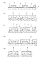
- a plurality of electronic components (IC or the like) 2 are mounted on a substrate 1 and a ground circuit pattern (copper foil) 3 is provided between the plurality of electronic components 2.
- the electronic component 2 is sealed by filling the electronic component 2 and the ground circuit pattern 3 with a sealing material 4 and curing it.
- the sealing material 4 is cut between the plurality of electronic components 2 to form grooves, and the packages of the electronic components on the substrate 1 are individualized by these grooves.
- Reference symbol A indicates an individual package. At least a part of the ground circuit is exposed from the wall surface constituting the groove, and the bottom of the groove does not completely penetrate the substrate.
- a predetermined amount of the binder component, the conductive filler and the curing agent described above and a solvent used as necessary are mixed to prepare a conductive resin composition.
- the conductive resin composition is sprayed in the form of a mist with a known spray gun or the like and applied evenly on the package surface.
- the spray pressure and spray flow rate at this time, and the distance between the spray gun spray port and the package surface are appropriately set as necessary.
- FIG. 2 is a plan view showing the substrate in this state.
- Reference numerals B 1 , B 2 ,... B 9 denote shield packages before being separated into individual pieces, and reference numerals 11 to 19 denote grooves between these shield packages, respectively.
- an individual package B is obtained by cutting the substrate with a dicing saw or the like along the bottom of the groove of the package before the individualization.
- the individual package B thus obtained has a uniform shield layer formed on the package surface (all of the upper surface portion, the side surface portion, and the corner portion of the boundary between the upper surface portion and the side surface portion). Good shielding characteristics can be obtained.
- the adhesion between the shield layer and the package surface and the ground circuit is excellent, it is possible to prevent the shield layer from being peeled off from the package surface or the ground circuit due to an impact when the package is separated into pieces by a dicing saw or the like. .
- Compound (b1) Liquid glycidylamine epoxy resin, manufactured by ADEKA Corporation, trade name “EP-3905S”
- Compound (b2) Liquid glycidyl ether epoxy resin, manufactured by ADEKA Corporation, trade name “EP-4400”
- Compound (b3) (meth) acrylate compound, 2-hydroxy-3-acryloyloxypropyl methacrylate (manufactured by Kyoeisha Chemical Co., Ltd., trade name “Light Ester G-201P”)
- ⁇ Curing agent> Compound having imidazole group (c1): 2-ethyl-4-methylimidazole (manufactured by Shikoku Kasei Kogyo Co., Ltd., trade name “2E4MZ”)
- Solvent Methyl ethyl ketone (MEK)
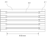
- Conductivity of conductive coating film The conductivity of the conductive coating film obtained from the conductive resin composition of Example 1 was evaluated by specific resistance. Specifically, as shown in FIG. 3, the electrode pad 21 formed of copper foil has a thickness of 55 ⁇ m provided with a slit having a width of 5 mm on the glass epoxy substrate 20 provided at both ends with an interval of 60 mm. The polyimide film was affixed so that the ends of the slits overlapped with the electrode pads 21 at both ends to form a printing plate. On top of that, the conductive resin compositions obtained in the examples and comparative examples were printed using a metal squeegee. The conductive resin composition is cured by heating at 190 ° C.
- the polyimide film is peeled off, and a cured product 22 having a length of 70 mm, a width of 5 mm, and a thickness of about 40 ⁇ m is connected between the electrode pads 21 at both ends.
- the substrate 20 formed in the above was obtained.
- the resistance value ((ohm)) between electrode pads was measured using a tester, and specific resistance ((omega
- the cross-sectional area, length, and specific resistance of the sample a total of 15 lines were formed by printing 5 lines each on 3 glass epoxy substrates, and the average value was obtained. If the specific resistance is 2 ⁇ 10 ⁇ 4 ⁇ ⁇ cm or less, it can be suitably used as a conductive resin composition used for the shield layer.
- Adhesiveness of conductive coating (comparison before and after solder dip) The adhesion between the shield layer and the package surface or the ground circuit was evaluated based on JIS K 5600-5-6: 1999 (cross cut method). Specifically, a copper foil was prepared for evaluation of adhesion to the ground circuit, and a mold resin for evaluation of adhesion to the package surface was prepared. Each is masked with a polyimide tape so as to form an opening having a width of 5 cm and a length of 10 cm, and after spray application of the conductive resin composition using a spray coating apparatus SL-940 (manufactured by Nordson Asymtek) at 190 ° C.
- SL-940 manufactured by Nordson Asymtek
- the evaluation of adhesion was performed according to the following criteria. 0: The edge of the cut is completely smooth and there is no peeling to the eyes of any lattice. 1: Small peeling of the coating film occurs at the intersection of cuts. The cross-cut portion is clearly not affected by more than 5%. 2: The coating film is peeled along the edge of the cut and / or at the intersection. The cross-cut part is clearly affected by more than 5% but not more than 15%. 3: The coating film is partially or completely peeled along the edge of the cut, and / or various parts of the eye are partially or completely peeled off. The cross-cut part is clearly affected by more than 15% but not more than 35%.
- the coating film is partially or completely peeled along the edge of the cut, and / or some eyes are partially or completely peeled off. It is clearly not more than 35% that the cross-cut is affected. 5: Any of the degree of peeling that cannot be classified even with classification 4.
- the color (hue H, lightness V, and saturation C) of the obtained cured coating film was examined according to JIS Z 8721 (1993). Next, these cured coating films were further heated at 200 ° C. for 60 minutes, and the colors of the cured coating films were examined in the same manner as described above. The color after further heating the cured coating film at 200 ° C. for 60 minutes is almost the same as the color of the cured coating film after the heat cycle test (200 cycles of ⁇ 65 ° C. for 30 minutes and 150 ° C. for 30 minutes). It has been confirmed in advance. The color change was evaluated according to the following criteria.
- Pass (O) The amount of change in viscosity before and after freezing was less than 20%.
- Fail (x) The amount of change in viscosity before and after freezing storage was 20% or more.
Landscapes
- Chemical & Material Sciences (AREA)
- Health & Medical Sciences (AREA)
- Chemical Kinetics & Catalysis (AREA)
- Medicinal Chemistry (AREA)
- Polymers & Plastics (AREA)
- Organic Chemistry (AREA)
- Compositions Of Macromolecular Compounds (AREA)
- Paints Or Removers (AREA)
- Shielding Devices Or Components To Electric Or Magnetic Fields (AREA)
- Structures Or Materials For Encapsulating Or Coating Semiconductor Devices Or Solid State Devices (AREA)
Abstract
良好なシールド性を有し、パッケージとの密着性が良好で、厳しい加熱条件下でも変色しにくいシールド層がスプレー塗布により形成可能な導電性樹脂組成物、及びこれを用いたシールドパッケージの製造方法を提供する。 (A)下記一般式(I)で表され、分子量が500~2000であり、1分子内に2以上のマレイミド基を有する化合物、(B)熱硬化性化合物、(C)イミダゾール基を有する化合物、及び(D)導電性フィラーを少なくとも含有する導電性樹脂組成物とする。
Description
本発明は、導電性樹脂組成物及びそれを用いたシールドパッケージの製造方法に関する。
携帯電話やタブレット端末等の電子機器においては、近年、大容量のデータを伝送するための無線通信用の電子部品を多数実装している。このような無線通信用の電子部品は、ノイズを発生しやすいだけでなくノイズに対する感受性が高く、外部からのノイズに曝されると誤動作を起こしやすいという問題を有する。
一方で、電子機器の小型軽量化と高機能化を両立させるため、電子部品の実装密度を高めることが求められている。しかしながら、実装密度を高めるとノイズの発生源となる電子部品が増えるだけでなく、ノイズの影響を受ける電子部品も増えてしまうという問題がある。
従来から、この課題を解決する手段として、ノイズの発生源である電子部品をパッケージごとシールド層で覆うことで、電子部品からのノイズの発生を防止するとともにノイズの侵入を防止した、いわゆるシールドパッケージが知られている。例えば特許文献1には、パッケージの表面に、導電性粒子を含有する導電性樹脂組成物をスプレー(噴霧)してコーティングし、加熱硬化することにより、シールド効果の高い電磁シールド部材を容易に得ることができる旨記載されている。
しかしながら、従来のシールドパッケージはハンダリフロー工程に投入すると、シールド層の色味が変化し、好ましい外観が得られにくいという問題を有する。これに対し、高純度の銀粒子を用いてシールド層を形成すれば変色を抑えることができるが、高価となるため、汎用性に欠けるものとなる。
一方で、銅粉または銀被覆銅粉を用いると、導電性樹脂組成物の価格は抑えられるが、導電性樹脂組成物を加熱硬化することで得られたシールド層の色味が変化するという問題を有する。
銅粉または銀被覆銅粉を用いた導電性樹脂組成物からなるシールド層が変色する要因は、樹脂組成物と銅粉または銀被覆銅粉との相互作用によるものと推測できる。従って、樹脂組成物中の銅粉または銀被覆銅粉の配合量を減らすことにより変色を抑えることが可能であると考えられる。しかしながら、樹脂組成物中の銅粉または銀被覆銅粉の配合量を減らせば、樹脂組成物の抵抗値が上昇するため、パッケージのシールド効果が低減するという問題が生じる。
本発明は上記に鑑みてなされたものであり、良好なシールド性を有するシールド層がスプレー塗布により形成可能な導電性樹脂組成物であって、得られたシールド層はパッケージとの密着性が良好で、厳しい加熱条件下でも変色しにくい導電性樹脂組成物を安価で提供することを目的とする。また、上記のようなシールド層が容易に形成可能なシールドパッケージの製造方法を提供することを目的とする。
本発明に係る導電性樹脂組成物は、(A)下記一般式(I)で表され、分子量が500~2000であり、1分子内に2以上のマレイミド基を有する化合物、(B)熱硬化性化合物、(C)イミダゾール基を有する化合物、及び(D)導電性フィラーを少なくとも含有するものとすることができる。

但し、式(I)中、Xは、脂肪族、脂環式、又は芳香族の炭化水素基であって、主鎖の炭素数が10~30である炭化水素基を示し、これらの基は、ヘテロ原子、置換基、又はシロキサン骨格を有していてもよい。
上記熱硬化性化合物(B)は、常温で固体であるエポキシ樹脂、常温で液体であるエポキシ樹脂、及び(メタ)アクリレート化合物からなる群より選択される少なくとも1種であるものとすることができる。
上記イミダゾール基を有する化合物(C)の含有量は、上記マレイミド基を有する化合物(A)と上記熱硬化性化合物(B)との合計量100質量部に対して、0.5~50質量部であるものとすることができる。
上記導電性フィラー(D)の含有量は、上記マレイミド基を有する化合物(A)と上記熱硬化性化合物(B)との合計量100質量部に対して、200~1800質量部であるものとすることができる。
上記導電性フィラー(D)は、銅粉、銀被覆銅粉、又は銀被覆銅合金粉であるものとすることができる。
本発明に係る導電性樹脂組成物は、電子部品のパッケージのシールド用とすることができる。
本発明に係るシールドパッケージの製造方法は、基板上に電子部品が搭載され、この電子部品が封止材によって封止されたパッケージがシールド層によって被覆されたシールドパッケージの製造方法であって、基板上に複数の電子部品を搭載し、この基板上に封止材を充填して硬化させることにより上記電子部品を封止する工程と、上記複数の電子部品間で封止材を切削して溝部を形成し、これらの溝部によって基板上の各電子部品のパッケージを個別化させる工程と、上記個別化したパッケージの表面に、上記導電性樹脂組成物を噴霧により塗布する工程と、上記パッケージの表面に導電性樹脂組成物が塗布された基板を加熱して、上記導電性樹脂組成物を硬化させることによりシールド層を形成する工程と、上記基板を上記溝部に沿って切断することにより個片化したシールドパッケージを得る工程とを少なくとも有するものとすることができる。
本発明の導電性樹脂組成物によれば、スプレー法により均一な厚みの塗膜を形成可能であり、得られた塗膜は厳しい加熱条件下でも変色を抑えることができる。従って、本発明の導電性樹脂組成物をパッケージ表面にスプレー塗布することにより、シールド効果と外観が優れ、かつパッケージとの密着性に優れたシールド層を容易に形成することが可能となる。
また本発明のシールドパッケージの製造方法によれば、上記のようなシールド性、耐変色性及びパッケージとの密着性に優れたシールドパッケージを、大がかりな装置を用いずに効率的に製造することができる。
A……基板上で個別化されたパッケージ、
B……個片化されたシールドパッケージ、
B1,B2,B9……個片化される前のシールドパッケージ、
1……基板、2……電子部品、3……グランド回路パターン(銅箔)、
4……封止材、5……シールド層(導電性塗膜)、11~19……溝、
20……基板、21……電極パッド、22……導電性樹脂組成物の硬化物
B……個片化されたシールドパッケージ、
B1,B2,B9……個片化される前のシールドパッケージ、
1……基板、2……電子部品、3……グランド回路パターン(銅箔)、
4……封止材、5……シールド層(導電性塗膜)、11~19……溝、
20……基板、21……電極パッド、22……導電性樹脂組成物の硬化物
本発明に係る導電性樹脂組成物は、上記の通り、(A)下記一般式(I)で表され、分子量が500~2000であり、1分子内に2以上のマレイミド基を有する化合物、(B)熱硬化性化合物、(C)イミダゾール基を有する化合物、及び(D)導電性フィラーを少なくとも含有する。この導電性樹脂組成物の用途は特に限定されるわけではないが、個片化される前のパッケージ又は個片化されたパッケージの表面に、スプレー等で霧状に噴射してシールド層を形成させてシールドパッケージを得るために好適に使用される。
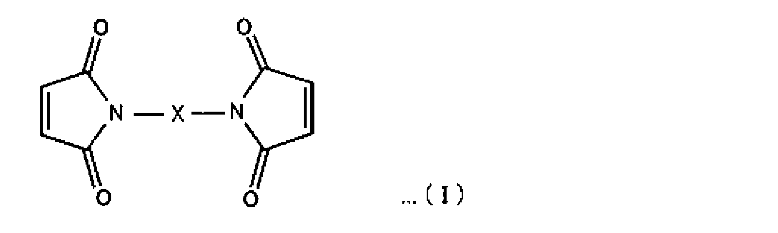
ここで、式(I)中、Xは、脂肪族、脂環式、又は芳香族の炭化水素基であって、主鎖の炭素数が10~30である炭化水素基を示し、これらの基は、ヘテロ原子、置換基、又はシロキサン骨格を有していてもよい。
Xは、好ましくは、脂肪族又は脂環式炭化水素基、若しくは脂環式炭化水素基により修飾された脂肪族炭化水素基であり、脂環式炭化水素基により修飾された脂肪族炭化水素基が特に好ましい。Xの主鎖の炭素数は10~30であることが好ましく、より好ましくは15~25である。Xの主鎖の炭素数が10~30の範囲内であると、イミダゾール基を有する化合物(C)と併用することにより、加熱硬化により得られたシールド層が黒化するため、ハンダリフロー工程に投入してもシールド層の変色は目立ちにくくなる。また、側鎖も含めた脂肪族炭化水素基としては炭素数が10~55であることがより好ましく、10~40であることがさらに好ましい。
上記化合物(A)の分子量は、500以上が好ましく、550以上であることがより好ましい。分子量が500以上であると、加熱硬化により得られたシールド層が黒化するため、ハンダリフロー工程に投入してもシールド層の変色は目立ちにくくなる。また、導電性樹脂組成物を保管中に導電性フィラーが沈降しにくくなる。さらに、導電性樹脂組成物をパッケージに塗布後、パッケージの壁面で液垂れすることを防ぐことができ、均一な塗膜を形成しやすくなる。
また、上記化合物(A)の分子量は、2000以下が好ましく、1000以下がより好ましく、900以下であることがさらに好ましい。分子量が2000以下であると、加熱硬化により得られたシールド層が黒化するため、ハンダリフロー工程に投入してもシールド層の変色は目立ちにくくなる。また、導電性樹脂組成物をパッケージに塗布後、均一な塗膜を形成しやすくなる。
上記化合物(A)の製造方法は特に限定されず、例えば酸無水物とジアミンとを縮合反応させたのち、脱水して環化(イミド化)を行う公知の方法により製造することができる。
その製造に使用可能な酸無水物の例としては、ポリブタジエン-グラフト-無水マレイン酸;ポリエチレン-グラフト-無水マレイン酸;ポリエチレン-無水マレイン酸交互共重合体;ポリ無水マレイン酸-1-オクタデセン交互共重合体;ポリプロピレン-グラフト-無水マレイン酸;ポリ(スチレン-無水マレイン酸)共重合体;無水ピロメリト酸;無水マレイン酸、無水コハク酸;1,2,3,4-シクロブタンテトラカルボン酸二無水物;1,4,5,8-ナフタレンテトラカルボン酸二無水物;3,4,9,10-ペリレンテトラカルボン酸二無水物;ビシクロ(2.2.2)オクト-7-エン-2,3,5,6-テトラカルボン酸二無水物;ジエチレントリアミンペンタ酢酸二無水物;エチレンジアミン四酢酸二無水物;3,3’,4,4’-ベンゾフェノンテトラカルボン酸二無水物;3,3’,4,4’-ビフェニルテトラカルボン酸二無水物;4,4’-オキシジフタリック無水物;3,3’,4,4’-ジフェニルスルホンテトラカルボン酸二無水物;2,2’-ビス(3,4-ジカルボキシフェニル)ヘキサフルオロプロパン二無水物;4,4’-ビスフェノールAジフタル酸無水物;5-(2,5-ジオキシテトラヒドロ)-3-メチル-3-シクロヘキセン-1,2-ジカルボン無水物;エチレングリコールビス(トリメリット酸無水物);ヒドロキノンジフタル酸無水物;アリルナディック酸無水物(allyl nadic anhydride);2-オクテン-1-イルコハク酸無水物;無水フタル酸;1,2,3,6-テトラヒドロフタル酸無水物;3,4,5,6-テトラヒドロフタル酸無水物;1,8-ナフタル酸無水物;グルタル酸無水物;ドデセニルコハク酸無水物;ヘキサデセニルコハク酸無水物;ヘキサヒドロフタル酸無水物;メチルヘキサヒドロフタル酸無水物;テトラデセニルコハク酸無水物等が挙げられる。
またジアミンの例としては、1,10-ジアミノデカン;1,12-ジアミノドデカン;ダイマージアミン;1,2-ジアミノ-2-メチルプロパン;1,2-ジアミノシクロヘキサン;1,2-ジアミノプロパン;1,3-ジアミノプロパン;1,4-ジアミノブタン;1,5-ジアミノペンタン;1,7-ジアミノヘプタン;1,8-ジアミノメンタン;1,8-ジアミノオクタン;1,9-ジアミノノナン;3,3’-ジアミノ-N-メチルジプロピルアミン;ジアミノマレオニトリル;1,3-ジアミノペンタン;9,10-ジアミノフェナントレン;4,4’-ジアミノオクタフルオロビフェニル;3,5-ジアミノ安息香酸;3,7-ジアミノ-2-メトキシフルオレン;4,4’-ジアミノベンゾフェノン;3,4-ジアミノベンゾフェノン;3,4-ジアミノトルエン;2,6-ジアミノアントラキノン;2,6-ジアミノトルエン;2,3-ジアミノトルエン;1,8-ジアミノナフタレン;2,4-ジアミノトルエン;2,5-ジアミノトルエン;1,4-ジアミノアントラキノン;1,5-ジアミノアントラキノン;1,5-ジアミノナフタレン;1,2-ジアミノアントラキノン;2,4-クメンジアミン;1,3-ビスアミノメチルベンゼン;1,3-ビスアミノメチルシクロヘキサン;2-クロロ-1,4-ジアミノベンゼン;1,4-ジアミノ-2,5-ジクロロベンゼン;1,4-ジアミノ-2,5-ジメチルベンゼン;4,4’-ジアミノ-2,2’-ビストリフルオロメチルビフェニル;ビス(アミノ-3-クロロフェニル)エタン;ビス(4-アミノ-3,5-ジメチルフェニル)メタン;ビス(4-アミノ-3,5-ジエチルフェニル)メタン;ビス(4-アミノ-3-エチルジアミノフルオレン;ジアミノ安息香酸;2,3-ジアミノナフタレン;2,3-ジアミノフェノール;-5-メチルフェニル)メタン;ビス(4-アミノ-3-メチルフェニル)メタン;ビス(4-アミノ-3-エチルフェニル)メタン;4,4’-ジアミノフェニルスルホン;3,3’-ジアミノフェニルスルホン;2,2-ビス(4-(4アミノフェノキシ)フェニル)スルホン;2,2-ビス(4-(3-アミノフェノキシ)フェニル)スルホン;4,4’-オキシジアニリン;4,4’-ジアミノジフェニルスルフィド;3,4’-オキシジアニリン;2,2-ビス(4-(4-アミノフェノキシ)フェニル)プロパン;1,3-ビス(4-アミノフェノキシ)ベンゼン;4,4’-ビス(4-アミノフェノキシ)ビフェニル;4,4’-ジアミノ-3,3’-ジヒドロキシビフェニル;4,4’-ジアミノ-3,3’-ジメチルビフェニル;4,4’-ジアミノ-3,3’-ジメトキシビフェニル;Bisaniline M;Bisaniline P;9,9-ビス(4-アミノフェニル)フルオレン;o-トリジンスルホン;メチレンビス(アントラニル酸);1,3-ビス(4-アミノフェノキシ)-2,2-ジメチルプロパン;1,3-ビス(4-アミノフェノキシ)プロパン;1,4-ビス(4-アミノフェノキシ)ブタン;1,5-ビス(4-アミノフェノキシ)ブタン;2,3,5,6-テトラメチル-1,4-フェニレンジアミン;3,3’,5,5’-テトラメチルベンジジン;4,4’-ジアミノベンザニリド;2,2-ビス(4-アミノフェニル)ヘキサフルオロプロパン;ポリオキシアルキレンジアミン類(たとえば、HuntsmanのJeffamine D-230、D400、D-2000およびD-4000);1,3-シクロヘキサンビス(メチルアミン);m-キシリレンジアミン;p-キシリレンジアミン;ビス(4-アミノ-3-メチルシクロヘキシル)メタン;1,2-ビス(2-アミノエトキシ)エタン;3(4),8(9)-ビス(アミノメチル)トリシクロ(5.2.1.02,6)デカン、1,2-ビス(アミノオクチル)-3-オクチル-4-ヘキシル-シクロヘキサン等が挙げられる。これらの中でも、優れた誘電特性や強度を示す樹脂含浸物及び硬化物を得る観点から、アルキル鎖の主鎖の炭素数が10~30であるジアミンであることが好ましい。
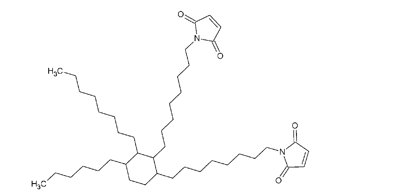
上記化合物(A)は、市販の化合物を用いることもでき、好ましい例としては、DESIGNER MOLECURES Inc.製のBMI-689(ダイマージアミン、マレイン酸無水物より合成)等を好適に用いることができる。BMI-689は、下記構造式で表される。
上記熱硬化性化合物(B)としては、特に限定されないが、エポキシ基を有する化合物、(メタ)アクリロイル基を有する化合物や、フェノール樹脂、メラミン樹脂、シリコン樹脂、アルキッド樹脂、キシレン樹脂等を使用することができる。これらは1種単独で用いてもよく、2種以上を併用してもよい。これらの中でもエポキシ基を有する化合物、または(メタ)アクリロイル基を有する化合物を含有することが好ましい。
上記のような熱硬化性化合物(B)を使用することで、ハンダリフロー工程に曝されても軟化せず、パッケージとしての機能を維持しやすい。
上記化合物(B)の含有量は、上記化合物(A)との合計量100質量部中、30~90質量部であることが好ましく、50~85質量部であることがより好ましい。以下、本明細書において、化合物(A)と化合物(B)との混合物をバインダー成分とする。
上記化合物(B)として、エポキシ基を有する化合物を用いる場合には、常温で固体のエポキシ樹脂(以下、「固体エポキシ樹脂」という場合がある)と、常温で液体のエポキシ樹脂(以下、「液体エポキシ樹脂」という場合がある)のいずれも用いることができる。
ここでエポキシ樹脂について「常温で固体」とは、25℃において無溶媒状態で流動性を有さない状態であることを意味するものとし、「常温で液体」とは同条件において流動性を有する状態であることを意味するものとする。
固体エポキシ樹脂は、溶剤に溶解して使用することができる。使用する溶剤は特に限定されず、後述するものの中から適宜選択することができる。
固体エポキシ樹脂の具体例としては、特にこれらに限定されないが、ビスフェノールA型エポキシ樹脂、ビスフェノールF型エポキシ樹脂、ビスフェノールS型エポキシ樹脂などのビスフェノール型エポキシ樹脂、スピロ環型エポキシ樹脂、ナフタレン型エポキシ樹脂、ビフェニル型エポキシ樹脂、テルペン型エポキシ樹脂、トリス(グリシジルオキシフェニル)メタン、テトラキス(グリシジルオキシフェニル)エタンなどのグリシジルエーテル型エポキシ樹脂、テトラグリシジルジアミノジフェニルメタンなどのグリシジルアミン型エポキシ樹脂、テトラブロムビスフェノールA型エポキシ樹脂、クレゾールノボラック型エポキシ樹脂、フェノールノボラック型エポキシ樹脂、α-ナフトールノボラック型エポキシ樹脂、臭素化フェノールノボラック型エポキシ樹脂等のノボラック型エポキシ樹脂、ゴム変性エポキシ樹脂等が挙げられる。これらは1種を単独で使用することもでき、2種以上を併用することもできる。
常温で液体のエポキシ樹脂の具体例としては、特に限定されないが、液体グリシジルアミン系エポキシ樹脂や、液体グリシジルエーテル系エポキシ樹脂等が挙げられ、液体グリシジルアミン系エポキシ樹脂であることが好ましい。
上記(メタ)アクリロイル基を有する化合物は、アクリロイル基又はメタクリロイル基を有する化合物であれば特に限定されないが、例えば、イソアミルアクリレート、ネオペンチルグリコールジアクリレート、トリメチロールプロパントリアクリレート、ジトリメチロールプロパンテトラアクリレート、2-ヒドロキシ-3-アクリロイロキシプロピルメタクリレート、フェニルグリシジルエーテルアクリレートヘキサメチレンジイソシアネートウレタンプレポリマー、ビスフェノールAジグリシジルエーテルアクリル酸付加物、エチレングリコールジメタクリレート、及びジエチレングリコールジメタクリレート等が挙げられる。これらは1種を単独で使用することもでき、2種以上を併用することもできる。
上記化合物(B)として、エポキシ基を有する化合物と、(メタ)アクリロイル基を有する化合物とを併用する場合、(メタ)アクリロイル基を有する化合物の含有割合は、エポキシ基を有する化合物と(メタ)アクリレート基を有する化合物との合計量中5~95質量%であることが好ましく、より好ましくは20~80質量%である。(メタ)アクリレート基を有する化合物が5質量%以上であることにより導電性樹脂組成物の保存安定性が優れ、導電性樹脂組成物を速やかに硬化させることができ、さらに硬化時の塗料ダレを防止することができる。また、(メタ)アクリレート基を有する化合物が95質量%以下である場合、パッケージとシールド層との密着性が良好となりやすい。
本発明においては、上記バインダー成分を硬化させるため、イミダゾール基を有する化合物(C)を使用する。硬化剤としてイミダゾール基を有する化合物(C)を用いることにより、本発明の導電性樹脂組成物からなる塗膜を加熱し硬化させてシールド層を形成した際に、得られたシールド層は黒化するため、ハンダリフロー工程に投入してもシールド層の変色は目立ちにくくなる。
本発明に使用するイミダゾール基を有する化合物(C)としては、特に限定されないが、例えば、イミダゾール、2-ウンデシルイミダゾール、2-ヘプタデシルイミダゾール、2-メチルイミダゾール、2-エチルイミダゾール、2-フェニルイミダゾール、2-エチル-4-メチル-イミダゾール、1-シアノエチル-2-ウンデシルイミダゾールが挙げられる。これらは1種単独で使用してもよく、2種以上を併用してもよい。
イミダゾール基を有する化合物(C)の含有量は、特に限定されないが、通常はバインダー成分100質量部に対して0.5~50質量部であることが好ましく、5~50質量部であることがより好ましい。イミダゾール基を有する化合物(C)の含有量が0.5質量部以上であると、シールド層とパッケージ表面との密着性とシールド層の導電性が良好となって、シールド効果に優れたシールド層が得られやすく、50質量部以下であると導電性樹脂組成物の保存安定性を良好に保ちやすい。また、イミダゾール基を有する化合物(C)に加えて、硬化剤としてラジカル系硬化剤を使用することも可能であり、その含有量は、バインダー成分100質量部に対して0.3~8質量部であることが好ましい。ラジカル系硬化剤の含有量が0.3質量部以上であると導電性塗膜と塗布対象物表面との密着性と導電性塗膜の導電性が良好となって、シールド効果に優れた導電性塗膜が得られやすく、8質量部以下であると導電性樹脂組成物の保存安定性が向上する。
本発明の導電性樹脂組成物における導電性フィラー(D)は、特に限定されないが、銅粉、銀粉、銀ナノ粉、銀被覆銅粉、又は銀被覆銅合金粉であることが好ましく、銅粉、銀被覆銅粉、又は銀被覆銅合金粉であることがより好ましい。銀被覆銅合金粉は、銅合金粉と、この銅合金粉を被覆する銀含有層とを有していてもよい。また、銅合金粉は、ニッケルの含有量が0.5~20質量%であり、かつ亜鉛の含有量が1~20質量%であってもよい。ニッケルと亜鉛とを上記した範囲内で含み、残部が銅からなり、残部の銅は不可避不純物を含んでいてもよい。このように銀被覆層を有する銅合金粉を用いることにより、シールド性に優れたシールドパッケージを得ることができる。
銀被覆量は、銀被覆銅粉中又は銀被覆銅合金粉中の割合で3~30質量%であることが好ましく、5~20質量%であることがより好ましい。銀被覆量が3質量%以上であると、厳しい加熱条件下でもシールドパッケージが変色するのを抑えやすく、かつ良好な導電性を得ることができる。銀被覆層が30質量%以下であると、シールド性に優れたパッケージを低コストで得ることができる。
上記導電性フィラー(D)の形状の例としては、フレーク状(鱗片状)、樹枝状、球状、繊維状、不定形(多面体)等が挙げられるが、抵抗値がより低く、シールド性がより向上したシールド層が得られる点からは、フレーク状であることが好ましい。
上記導電性フィラー(D)がフレーク状である場合は、導電性フィラー(D)のタップ密度は4.0~6.5g/cm3であることが好ましい。タップ密度が上記範囲内であると、シールド層の導電性がより良好となる。
また、上記導電性フィラー(D)がフレーク状である場合には、導電性フィラー(D)のアスペクト比は2~10であることが好ましい。アスペクト比が上記範囲内であると、シールド層の導電性がより良好となる。
上記導電性フィラー(D)の平均粒径は、1~30μmであることが好ましい。導電性フィラー(D)の平均粒径が1μm以上であると、導電性フィラー(D)の分散性が良好で凝集が防止でき、また酸化されにくく、30μm以下であるとパッケージのグランド回路との接続性が良好である。
上記導電性フィラー(D)の含有量は、特に限定されないが、バインダー成分100質量部に対して200~1800質量部であることが好ましい。その含有量が200質量部以上であるとシールド層の導電性が良好となり、1800質量部以下であると、シールド層とパッケージとの密着性、及び硬化後の導電性樹脂組成物の物性が良好となり、後述するダイシングソーで切断した時にシールド層のカケが生じにくくなる。また、導電性塗料を加熱硬化後、樹脂の黒色化により放置しても変色が目立ちにくくなる。
また、本発明の導電性樹脂組成物には、発明の目的を損なわない範囲内において、消泡剤、増粘剤、粘着剤、充填剤、難燃剤、着色剤等、公知の添加剤を加えることができる。
本発明の導電性樹脂組成物は、導電性樹脂組成物をスプレー噴霧によりパッケージ表面に均一に塗布できるようにするためには、いわゆる導電性ペーストよりも低粘度であることが好ましい。
本発明の導電性樹脂組成物の粘度は、用途や塗布に使用する機器に応じて適宜調整するのが好ましく、特に限定されないが、一般的な目安としては以下に述べる通りである。粘度の測定方法も限定されるものではないが、導電性樹脂組成物が低粘度であれば円錐平板型回転粘度計(いわゆるコーン・プレート型粘度計)で測定することができ、高粘度であれば単一円筒形回転粘度計(いわゆるB型又はBH型粘度計)で測定することができる。
円錐平板型回転粘度計で測定する場合は、ブルックフィールド(BROOK FIELD)社のコーンスピンドルCP40(コーン角度:0.8°、コーン半径:24mm)を用いて、0.5rpmで測定した粘度が100mPa・s以上であることが好ましく、150mPa・s以上であることがより好ましい。粘度が100mPa・s以上であると、塗布面が水平でない場合における液ダレを防止して導電性塗膜をムラなく形成しやすい。なお、100mPa・s付近やそれよりも低粘度の場合、所望の厚さの均一な塗膜を得るには、1回の塗布量を少なくして薄膜を形成し、その上にまた薄膜を形成する操作をくり返す、いわゆる重ね塗りを行う方法が有効である。なお、円錐平板型回転粘度計で測定可能な粘度であれば、高くとも問題はない。
単一円筒形回転粘度計で測定する場合はローターNo.5を用いて10rpmで測定した粘度が30dPa・s以下であることが好ましく、25dPa・s以下であることがより好ましい。30dPa・s以下であるとスプレーノズルの目詰まりを防ぎ、ムラなく導電性塗膜を形成しやすい。なお、単一円筒形回転粘度計で測定可能な粘度であれば、低くとも問題はない。
導電性樹脂組成物の粘度はバインダー成分の粘度や導電性フィラーの含有量等により異なるので、上記範囲内にするために、溶剤を使用することができる。本発明において使用可能な溶剤は、特に限定されないが、例えば、プロピレングリコールモノメチルエーテル、3-メトキシ-3-メチル-1-ブチルアセテート、アセトン、メチルエチルケトン、アセトフェノン、メチルセロソルブ、メチルセロソルブアセテート、メチルカルビトール、ジエチレングリコールジメチルエーテル、テトラヒドロフラン、酢酸ブチル、酢酸メチル等が挙げられる。これらは1種を単独で使用することもでき、2種以上を併用してもよい。
溶剤の含有量は、導電性樹脂組成物の用途や塗布に使用する機器等に応じて適宜調整するのが好ましい。従って、バインダー成分の粘度や導電性フィラーの含有量等により異なるが、目安としては、導電性樹脂組成物の含有成分(溶剤を除く)の合計量に対して10~60質量%程度である。
本発明の導電性樹脂組成物によって得られるシールド層は、銅箔等で形成されたグランド回路との密着性に優れる。具体的には、シールドパッケージの一部から露出したグランド回路の銅箔とシールド層との密着性が良好であるため、シールドパッケージ表面に導電性樹脂組成物を塗布してシールド層を形成した後にパッケージを切断して個片化する際、切断時の衝撃によりシールド層がグランド回路から剥離することを防ぐことができる。
本発明の導電性樹脂組成物により形成される塗膜は、シールド層として使用する場合は、優れたシールド特性が得られる点から比抵抗が2×10⁻⁴Ω・cm以下であることが好ましい。
次に、本発明の導電性樹脂組成物を用いてシールドパッケージを得るための方法の一実施形態について図を用いて説明する。
まず、図1(a)に示すように、基板1に複数の電子部品(IC等)2を搭載し、これら複数の電子部品2間にグランド回路パターン(銅箔)3が設けられたものを用意する。
次に、同図(b)に示すように、これら電子部品2及びグランド回路パターン3上に封止材4を充填して硬化させ、電子部品2を封止する。
次に、同図(c)において矢印で示すように、複数の電子部品2間で封止材4を切削して溝部を形成し、これらの溝部によって基板1の各電子部品のパッケージを個別化させる。符号Aは、それぞれ個別化したパッケージを示す。溝を構成する壁面からはグランド回路の少なくとも一部が露出しており、溝の底部は基板を完全には貫通していない。
一方で、上述したバインダー成分、導電性フィラー及び硬化剤の所定量と、必要に応じて使用される溶剤を混合し、導電性樹脂組成物を用意する。
次いで、導電性樹脂組成物を公知のスプレーガン等によって霧状に噴射し、パッケージ表面にまんべんなく塗布する。このときの噴射圧力や噴射流量、スプレーガンの噴射口とパッケージ表面との距離は、必要に応じて適宜設定される。
次に、導電性樹脂組成物が塗布されたパッケージを加熱して溶剤を十分に乾燥させた後、さらに加熱して導電性樹脂組成物を十分に硬化させ、同図(d)に示すように、パッケージ表面にシールド層(導電性塗膜)5を形成させる。このときの加熱条件は適宜設定することができる。図2はこの状態における基板を示す平面図である。符号B1,B2,…B9は、個片化される前のシールドパッケージをそれぞれ示し、符号11~19はこれらシールドパッケージ間の溝をそれぞれ表す。
次に、図1(e)において矢印で示すように、個片化前のパッケージの溝の底部に沿って基板をダイシングソー等により切断することにより個片化されたパッケージBが得られる。
このようにして得られる個片化されたパッケージBは、パッケージ表面(上面部、側面面部及び上面部と側面部との境界の角部のいずれも)に均一なシールド層が形成されているため、良好なシールド特性が得られる。またシールド層とパッケージ表面及びグランド回路との密着性に優れているため、ダイシングソー等によってパッケージを個片化する際の衝撃によりパッケージ表面やグランド回路からシールド層が剥離することを防ぐことができる。
以下、本発明の内容を実施例に基づいて詳細に説明するが、本発明は以下に限定されるものではない。また、以下において「部」又は「%」とあるのは、特にことわらない限り質量基準とする。
[実施例、比較例]
次に示す1分子内に2以上のマレイミド基を有する化合物(a1,a2)と、熱硬化性化合物(b1~b3)との合計量100質量部に対して、硬化剤、導電性フィラー(d)、及び溶剤を表1に記載された割合で配合して混合し、導電性樹脂組成物を得た。使用した各成分の詳細は以下の通りである。
次に示す1分子内に2以上のマレイミド基を有する化合物(a1,a2)と、熱硬化性化合物(b1~b3)との合計量100質量部に対して、硬化剤、導電性フィラー(d)、及び溶剤を表1に記載された割合で配合して混合し、導電性樹脂組成物を得た。使用した各成分の詳細は以下の通りである。
化合物(a1):DESIGNER MOLECURES Inc.製、商品名「BMI-689」、重量平均分子量=約689
化合物(a2):DESIGNER MOLECURES Inc.製、商品名「BMI-3000」、重量平均分子量=約3000
化合物(a2):DESIGNER MOLECURES Inc.製、商品名「BMI-3000」、重量平均分子量=約3000
化合物(b1):液体グリシジルアミン系エポキシ樹脂、(株)ADEKA製、商品名「EP-3905S」
化合物(b2):液体グリシジルエーテル系エポキシ樹脂、(株)ADEKA製、商品名「EP-4400」
化合物(b3):(メタ)アクリレート化合物、2-ヒドロキシ-3-アクリロイロキシプロピルメタクリレート(共栄社化学(株)製、商品名「ライトエステルG-201P」)
化合物(b2):液体グリシジルエーテル系エポキシ樹脂、(株)ADEKA製、商品名「EP-4400」
化合物(b3):(メタ)アクリレート化合物、2-ヒドロキシ-3-アクリロイロキシプロピルメタクリレート(共栄社化学(株)製、商品名「ライトエステルG-201P」)
<硬化剤>
イミダゾール基を有する化合物(c1):2-エチル-4-メチルイミダゾール(四国化成工業(株)製、商品名「2E4MZ」)
イミダゾール基を有する化合物(c2):2-ウンデシルイミダゾール(四国化成工業(株)製、商品名「C11Z」)
アミン系化合物:ポリアミン系硬化剤((株)T&K TOKA製、商品名「フジキュアーFXR-1030」)
イミダゾール基を有する化合物(c1):2-エチル-4-メチルイミダゾール(四国化成工業(株)製、商品名「2E4MZ」)
イミダゾール基を有する化合物(c2):2-ウンデシルイミダゾール(四国化成工業(株)製、商品名「C11Z」)
アミン系化合物:ポリアミン系硬化剤((株)T&K TOKA製、商品名「フジキュアーFXR-1030」)
導電性フィラー(d):銀被覆銅合金粉(平均粒径=5μm、フレーク状、アスペクト比=2~10、タップ密度=5.8g/cm3)
溶剤:メチルエチルケトン(MEK)
溶剤:メチルエチルケトン(MEK)
上記実施例及び比較例の導電性樹脂組成物の評価を以下の通り行った。結果を表1に示す。
(1)導電性塗膜の導電性
実施例1の導電性樹脂組成物から得られた導電性塗膜の導電性を、比抵抗で評価した。具体的には、図3に示すように、銅箔で形成された電極パッド21が60mmの間隔をあけて両端に設けられたガラスエポキシ基板20上に、幅5mmのスリットを設けた厚さ55μmのポリイミドフィルムを、スリットの端部が両端の電極パッド21と重なるように貼り付けて印刷版とした。その上に、各実施例及び比較例で得られた導電性樹脂組成物を、金属スキージを用いて印刷した。190℃で20分間加熱することにより導電性樹脂組成物を硬化させ、ポリイミドフィルムを剥離し、長さ70mm、幅5mm、厚さ約40μmの硬化物22が両端の電極パッド21間を接続するように形成された基板20を得た。この硬化物サンプルにつき、テスターを用いて電極パッド間の抵抗値(Ω)を測定し、断面積(S、cm2)と長さ(L、cm)から次式(1)により比抵抗(Ω・cm)を計算した。
実施例1の導電性樹脂組成物から得られた導電性塗膜の導電性を、比抵抗で評価した。具体的には、図3に示すように、銅箔で形成された電極パッド21が60mmの間隔をあけて両端に設けられたガラスエポキシ基板20上に、幅5mmのスリットを設けた厚さ55μmのポリイミドフィルムを、スリットの端部が両端の電極パッド21と重なるように貼り付けて印刷版とした。その上に、各実施例及び比較例で得られた導電性樹脂組成物を、金属スキージを用いて印刷した。190℃で20分間加熱することにより導電性樹脂組成物を硬化させ、ポリイミドフィルムを剥離し、長さ70mm、幅5mm、厚さ約40μmの硬化物22が両端の電極パッド21間を接続するように形成された基板20を得た。この硬化物サンプルにつき、テスターを用いて電極パッド間の抵抗値(Ω)を測定し、断面積(S、cm2)と長さ(L、cm)から次式(1)により比抵抗(Ω・cm)を計算した。

サンプルの断面積、長さ及び比抵抗は、ガラスエポキシ基板3枚に各5本のライン印刷を施して合計15本形成し、その平均値を求めた。なお、比抵抗が2×10⁻⁴Ω・cm以下であれば、シールド層に用いる導電性樹脂組成物として好適に使用できる。
また、他の実施例及び比較例についても同様に比抵抗を測定した。
(2)導電性塗膜の密着性(ハンダディップ前後の比較)
シールド層とパッケージ表面又はグランド回路との密着性を、JIS K 5600-5-6:1999(クロスカット法)に基づき評価した。具体的には、グランド回路との密着性評価用に銅箔を用意し、パッケージ表面との密着性評価用のモールド樹脂を用意した。それぞれに、幅5cm、長さ10cmの開口部を形成するようにポリイミドテープでマスキングし、スプレーコーティング装置SL-940(Nordson Asymtek製)を用いて導電性樹脂組成物をスプレー塗布後、190℃で20分間加熱することにより硬化させ、ポリイミドテープを剥離し、厚さ約15μmの塗膜を形成した。塗膜が形成された銅箔、及びモールド樹脂上でクロスカット試験を行った。クロスカット試験は、リフロー前と、250℃で10秒間のリフロー処理を3回行ったものについて実施した。
シールド層とパッケージ表面又はグランド回路との密着性を、JIS K 5600-5-6:1999(クロスカット法)に基づき評価した。具体的には、グランド回路との密着性評価用に銅箔を用意し、パッケージ表面との密着性評価用のモールド樹脂を用意した。それぞれに、幅5cm、長さ10cmの開口部を形成するようにポリイミドテープでマスキングし、スプレーコーティング装置SL-940(Nordson Asymtek製)を用いて導電性樹脂組成物をスプレー塗布後、190℃で20分間加熱することにより硬化させ、ポリイミドテープを剥離し、厚さ約15μmの塗膜を形成した。塗膜が形成された銅箔、及びモールド樹脂上でクロスカット試験を行った。クロスカット試験は、リフロー前と、250℃で10秒間のリフロー処理を3回行ったものについて実施した。
密着性の評価は、次の基準で行った。
0:カットの縁が完全に滑らかで、どの格子の目にもはがれがない。
1:カットの交差点において塗膜の小さなはがれが生じている。クロスカット部分で影響を受けるのは明確に5%を上回ることはない。
2:塗膜がカットの縁に沿って、及び/又は交差点においてはがれている。クロスカット部分で影響を受けるのは明確に5%を越えるが15%を上回ることはない。
3:塗膜がカットの縁に沿って、部分的又は全面的に大はがれを生じており、及び/又は目のいろいろな部分が、部分的又は全面的にはがれている。クロスカット部分で影響を受けるのは、明確に15%を越えるが35%を上回ることはない。
4:塗膜がカットの縁に沿って、部分的又は全面的に大はがれを生じており、及び/又は数カ所の目が部分的又全面的にはがれている。クロスカット部分で影響を受けるのは、明確に35%を上回ることはない。
5:分類4でも分類できないはがれ程度のいずれか。
0:カットの縁が完全に滑らかで、どの格子の目にもはがれがない。
1:カットの交差点において塗膜の小さなはがれが生じている。クロスカット部分で影響を受けるのは明確に5%を上回ることはない。
2:塗膜がカットの縁に沿って、及び/又は交差点においてはがれている。クロスカット部分で影響を受けるのは明確に5%を越えるが15%を上回ることはない。
3:塗膜がカットの縁に沿って、部分的又は全面的に大はがれを生じており、及び/又は目のいろいろな部分が、部分的又は全面的にはがれている。クロスカット部分で影響を受けるのは、明確に15%を越えるが35%を上回ることはない。
4:塗膜がカットの縁に沿って、部分的又は全面的に大はがれを生じており、及び/又は数カ所の目が部分的又全面的にはがれている。クロスカット部分で影響を受けるのは、明確に35%を上回ることはない。
5:分類4でも分類できないはがれ程度のいずれか。
(3)導電性塗膜の変色試験(加熱前後の色調変化の測定)
本発明の導電性樹脂組成物を加熱硬化した後の塗膜の色調を評価した。具体的には、ガラスプレート上に幅1.5cm、長さ4.0cmの開口部を形成するようにポリイミドテープを用いてマスキングし、スプレーコーティング装置SL-940(Nordson Asymtek製)を用いて導電性樹脂組成物をスプレー塗布後、190℃で20分間加熱することにより硬化させ、ポリイミドテープを剥離し、厚さ20μmの硬化塗膜を得た。得られた硬化塗膜の色(色相H、明度V、及び彩度C)を、JIS Z 8721(1993)に準拠して調べた。次に、これらの硬化塗膜をさらに200℃で60分間加熱し、上記と同様に硬化塗膜の色を調べた。なお、硬化塗膜をさらに200℃で60分間加熱した後の色は、ヒートサイクル試験(-65℃で30分間と150℃で30分間を200サイクル)後の硬化塗膜の色とほぼ同等であることを、予め確認済である。色の変化は、次の基準で評価した。
本発明の導電性樹脂組成物を加熱硬化した後の塗膜の色調を評価した。具体的には、ガラスプレート上に幅1.5cm、長さ4.0cmの開口部を形成するようにポリイミドテープを用いてマスキングし、スプレーコーティング装置SL-940(Nordson Asymtek製)を用いて導電性樹脂組成物をスプレー塗布後、190℃で20分間加熱することにより硬化させ、ポリイミドテープを剥離し、厚さ20μmの硬化塗膜を得た。得られた硬化塗膜の色(色相H、明度V、及び彩度C)を、JIS Z 8721(1993)に準拠して調べた。次に、これらの硬化塗膜をさらに200℃で60分間加熱し、上記と同様に硬化塗膜の色を調べた。なお、硬化塗膜をさらに200℃で60分間加熱した後の色は、ヒートサイクル試験(-65℃で30分間と150℃で30分間を200サイクル)後の硬化塗膜の色とほぼ同等であることを、予め確認済である。色の変化は、次の基準で評価した。
合格(○):明度Vが変化しないか、2段階未満の変化(例えばV6からV5へと変化)であった。
不合格(×):明度Vの2段階以上の変化があった。
不合格(×):明度Vの2段階以上の変化があった。
表1に記載のとおり、各実施例では加熱硬化後の変色が抑えられていたが、比較例1~3においては、いずれも明度Vについて2段階の変化が見られ、著しく変色していた。
(4)導電性樹脂組成物の保存安定性
上記各実施例及び比較例で得られた導電性樹脂組成物の溶剤の含有量を5質量%となるように調製し、3ヶ月間冷凍保存した。冷凍保存前と冷凍保存後の導電性樹脂組成物について、BH型粘度計又は円錐平板型回転粘度計を用いて、組成物の温度25℃における粘度を測定した。BH型粘度計での粘度測定はローターNo.5を用いて、回転数10rpmで行った。円錐平板型回転粘度計での粘度測定は、ブルックフィールド(BROOK FIELD)社のプログラマブル粘度計「DV-II+Pro」、コーンスピンドルCP40を用いて、0.5rpmで行った。
上記各実施例及び比較例で得られた導電性樹脂組成物の溶剤の含有量を5質量%となるように調製し、3ヶ月間冷凍保存した。冷凍保存前と冷凍保存後の導電性樹脂組成物について、BH型粘度計又は円錐平板型回転粘度計を用いて、組成物の温度25℃における粘度を測定した。BH型粘度計での粘度測定はローターNo.5を用いて、回転数10rpmで行った。円錐平板型回転粘度計での粘度測定は、ブルックフィールド(BROOK FIELD)社のプログラマブル粘度計「DV-II+Pro」、コーンスピンドルCP40を用いて、0.5rpmで行った。
冷凍保存前と冷凍保存後の粘度の変化量に基づき次の基準で評価した。
合格(○):冷凍保存前後の粘度の変化量が20%未満であった。
不合格(×):冷凍保存前後の粘度の変化量が20%以上であった。
合格(○):冷凍保存前後の粘度の変化量が20%未満であった。
不合格(×):冷凍保存前後の粘度の変化量が20%以上であった。

表1に示す結果から、各実施例の導電性樹脂組成物により得られる塗膜はいずれも良好な導電性を有するのみならず、密着性も良好で、厳しい加熱条件下でも変色しにくいことが確認された。また、保存安定性にも優れていた。
Claims (7)
- (A)下記一般式(I)で表され、分子量が500~2000であり、1分子内に2以上のマレイミド基を有する化合物、
(B)熱硬化性化合物、
(C)イミダゾール基を有する化合物、及び
(D)導電性フィラー
を少なくとも含有する、導電性樹脂組成物。

- 前記熱硬化性化合物(B)が、
常温で固体であるエポキシ樹脂、常温で液体であるエポキシ樹脂、及び(メタ)アクリレート化合物からなる群より選択される少なくとも1種である、
請求項1に記載の導電性樹脂組成物。 - 前記イミダゾール基を有する化合物(C)の含有量が、前記マレイミド基を有する化合物(A)と前記熱硬化性化合物(B)との合計量100質量部に対して、0.5~50質量部である、請求項1又は2に記載の導電性樹脂組成物。
- 前記導電性フィラー(D)の含有量が、前記マレイミド基を有する化合物(A)と前記熱硬化性化合物(B)との合計量100質量部に対して、200~1800質量部である、請求項1~3のいずれか1項に記載の導電性樹脂組成物。
- 前記導電性フィラー(D)が、銅粉、銀被覆銅粉、又は銀被覆銅合金粉である、請求項1~4のいずれか1項に記載の導電性樹脂組成物。
- 電子部品のパッケージのシールド用である、請求項1~5のいずれか1項に記載の導電性樹脂組成物。
- 基板上に電子部品が搭載され、この電子部品が封止材によって封止されたパッケージがシールド層によって被覆されたシールドパッケージの製造方法であって、
基板上に複数の電子部品を搭載し、この基板上に封止材を充填して硬化させることにより前記電子部品を封止する工程と、
前記複数の電子部品間で封止材を切削して溝部を形成し、これらの溝部によって基板上の各電子部品のパッケージを個別化させる工程と、
前記個別化したパッケージの表面に、請求項1~6のいずれか1項に記載の導電性樹脂組成物を噴霧により塗布する工程と、
前記パッケージの表面に導電性樹脂組成物が塗布された基板を加熱して、前記導電性樹脂組成物を硬化させることによりシールド層を形成する工程と、
前記基板を前記溝部に沿って切断することにより個片化したシールドパッケージを得る工程と
を少なくとも有する、シールドパッケージの製造方法。
Priority Applications (2)
| Application Number | Priority Date | Filing Date | Title |
|---|---|---|---|
| CN201880017919.8A CN110382620A (zh) | 2017-06-15 | 2018-04-03 | 导电性树脂组合物及使用该导电性树脂组合物的屏蔽封装体的制造方法 |
| KR1020197025414A KR20200019593A (ko) | 2017-06-15 | 2018-04-03 | 도전성 수지 조성물 및 그것을 사용한 차폐 패키지의 제조 방법 |
Applications Claiming Priority (2)
| Application Number | Priority Date | Filing Date | Title |
|---|---|---|---|
| JP2017117814A JP2019001912A (ja) | 2017-06-15 | 2017-06-15 | 導電性樹脂組成物及びそれを用いたシールドパッケージの製造方法 |
| JP2017-117814 | 2017-06-15 |
Publications (1)
| Publication Number | Publication Date |
|---|---|
| WO2018230109A1 true WO2018230109A1 (ja) | 2018-12-20 |
Family
ID=64660003
Family Applications (1)
| Application Number | Title | Priority Date | Filing Date |
|---|---|---|---|
| PCT/JP2018/014287 Ceased WO2018230109A1 (ja) | 2017-06-15 | 2018-04-03 | 導電性樹脂組成物及びそれを用いたシールドパッケージの製造方法 |
Country Status (5)
| Country | Link |
|---|---|
| JP (1) | JP2019001912A (ja) |
| KR (1) | KR20200019593A (ja) |
| CN (1) | CN110382620A (ja) |
| TW (1) | TW201904764A (ja) |
| WO (1) | WO2018230109A1 (ja) |
Families Citing this family (3)
| Publication number | Priority date | Publication date | Assignee | Title |
|---|---|---|---|---|
| JP7272284B2 (ja) * | 2020-01-15 | 2023-05-12 | 信越化学工業株式会社 | 低誘電樹脂組成物 |
| CN111508911B (zh) * | 2020-04-30 | 2022-03-25 | 青岛歌尔微电子研究院有限公司 | 分腔电磁屏蔽封装方法及封装结构 |
| TW202444786A (zh) * | 2023-03-09 | 2024-11-16 | 日商拓自達電線股份有限公司 | 導電性組成物 |
Citations (5)
| Publication number | Priority date | Publication date | Assignee | Title |
|---|---|---|---|---|
| JP2003258137A (ja) * | 2002-02-28 | 2003-09-12 | Mitsubishi Electric Corp | 半導体装置 |
| JP2008063449A (ja) * | 2006-09-07 | 2008-03-21 | Hitachi Ltd | ポリマーナノコンポジット材料、その製造方法電子部品装置およびその製造方法 |
| JP2009179725A (ja) * | 2008-01-31 | 2009-08-13 | Sumitomo Bakelite Co Ltd | 樹脂組成物およびそれを用いて作製した半導体装置または回路基板 |
| WO2016051700A1 (ja) * | 2014-09-30 | 2016-04-07 | タツタ電線株式会社 | 導電性塗料及びそれを用いたシールドパッケージの製造方法 |
| JP2017008160A (ja) * | 2015-06-18 | 2017-01-12 | 京セラ株式会社 | ダイボンディングペーストの製造方法およびダイボンディングペースト |
Family Cites Families (1)
| Publication number | Priority date | Publication date | Assignee | Title |
|---|---|---|---|---|
| JP5266719B2 (ja) * | 2007-10-29 | 2013-08-21 | 住友ベークライト株式会社 | 樹脂組成物及び樹脂組成物を使用して作製した半導体装置 |
-
2017
- 2017-06-15 JP JP2017117814A patent/JP2019001912A/ja active Pending
-
2018
- 2018-04-03 CN CN201880017919.8A patent/CN110382620A/zh active Pending
- 2018-04-03 WO PCT/JP2018/014287 patent/WO2018230109A1/ja not_active Ceased
- 2018-04-03 KR KR1020197025414A patent/KR20200019593A/ko not_active Ceased
- 2018-04-17 TW TW107113043A patent/TW201904764A/zh unknown
Patent Citations (5)
| Publication number | Priority date | Publication date | Assignee | Title |
|---|---|---|---|---|
| JP2003258137A (ja) * | 2002-02-28 | 2003-09-12 | Mitsubishi Electric Corp | 半導体装置 |
| JP2008063449A (ja) * | 2006-09-07 | 2008-03-21 | Hitachi Ltd | ポリマーナノコンポジット材料、その製造方法電子部品装置およびその製造方法 |
| JP2009179725A (ja) * | 2008-01-31 | 2009-08-13 | Sumitomo Bakelite Co Ltd | 樹脂組成物およびそれを用いて作製した半導体装置または回路基板 |
| WO2016051700A1 (ja) * | 2014-09-30 | 2016-04-07 | タツタ電線株式会社 | 導電性塗料及びそれを用いたシールドパッケージの製造方法 |
| JP2017008160A (ja) * | 2015-06-18 | 2017-01-12 | 京セラ株式会社 | ダイボンディングペーストの製造方法およびダイボンディングペースト |
Also Published As
| Publication number | Publication date |
|---|---|
| KR20200019593A (ko) | 2020-02-24 |
| CN110382620A (zh) | 2019-10-25 |
| JP2019001912A (ja) | 2019-01-10 |
| TW201904764A (zh) | 2019-02-01 |
Similar Documents
| Publication | Publication Date | Title |
|---|---|---|
| US9236169B2 (en) | Electromagnetic wave shielding structure and method for fabricating the same | |
| KR101725748B1 (ko) | 전자 부품의 패키지의 쉴드용 도전성 도료 및 이것을 이용한 쉴드 패키지의 제조 방법 | |
| TWI722136B (zh) | 導電性塗料及使用其之屏蔽封裝體之製造方法 | |
| US10294324B2 (en) | Resin composition, conductive resin composition, adhesive, conductive adhesive, paste for forming electrodes, and semiconductor device | |
| JP6992083B2 (ja) | シールドパッケージ | |
| JP6831731B2 (ja) | 導電性塗料及びそれを用いたシールドパッケージの製造方法 | |
| US20180222152A1 (en) | Resin-clad copper foil, and printed wiring board | |
| WO2018230109A1 (ja) | 導電性樹脂組成物及びそれを用いたシールドパッケージの製造方法 | |
| JP7464044B2 (ja) | 磁性粉体を含む樹脂組成物 | |
| WO2018012017A1 (ja) | 導電性塗料及びそれを用いたシールドパッケージの製造方法 | |
| JP2020055977A (ja) | 導電性塗料 | |
| HK1229833A1 (en) | Conductive coating material and method for producing shield package using same | |
| HK40002728A (zh) | 导电性胶粘剂组合物 |
Legal Events
| Date | Code | Title | Description |
|---|---|---|---|
| 121 | Ep: the epo has been informed by wipo that ep was designated in this application |
Ref document number: 18818213 Country of ref document: EP Kind code of ref document: A1 |
|
| ENP | Entry into the national phase |
Ref document number: 20197025414 Country of ref document: KR Kind code of ref document: A |
|
| NENP | Non-entry into the national phase |
Ref country code: DE |
|
| 122 | Ep: pct application non-entry in european phase |
Ref document number: 18818213 Country of ref document: EP Kind code of ref document: A1 |