WO2018220910A1 - 表面被覆立方晶窒化硼素焼結体およびこれを備える切削工具 - Google Patents
表面被覆立方晶窒化硼素焼結体およびこれを備える切削工具 Download PDFInfo
- Publication number
- WO2018220910A1 WO2018220910A1 PCT/JP2018/006170 JP2018006170W WO2018220910A1 WO 2018220910 A1 WO2018220910 A1 WO 2018220910A1 JP 2018006170 W JP2018006170 W JP 2018006170W WO 2018220910 A1 WO2018220910 A1 WO 2018220910A1
- Authority
- WO
- WIPO (PCT)
- Prior art keywords
- coating
- boron nitride
- cubic boron
- interface
- less
- Prior art date
- Legal status (The legal status is an assumption and is not a legal conclusion. Google has not performed a legal analysis and makes no representation as to the accuracy of the status listed.)
- Ceased
Links
Images

Classifications
-
- B—PERFORMING OPERATIONS; TRANSPORTING
- B23—MACHINE TOOLS; METAL-WORKING NOT OTHERWISE PROVIDED FOR
- B23B—TURNING; BORING
- B23B27/00—Tools for turning or boring machines; Tools of a similar kind in general; Accessories therefor
- B23B27/14—Cutting tools of which the bits or tips or cutting inserts are of special material
-
- B—PERFORMING OPERATIONS; TRANSPORTING
- B23—MACHINE TOOLS; METAL-WORKING NOT OTHERWISE PROVIDED FOR
- B23B—TURNING; BORING
- B23B27/00—Tools for turning or boring machines; Tools of a similar kind in general; Accessories therefor
- B23B27/14—Cutting tools of which the bits or tips or cutting inserts are of special material
- B23B27/18—Cutting tools of which the bits or tips or cutting inserts are of special material with cutting bits or tips or cutting inserts rigidly mounted, e.g. by brazing
- B23B27/20—Cutting tools of which the bits or tips or cutting inserts are of special material with cutting bits or tips or cutting inserts rigidly mounted, e.g. by brazing with diamond bits or cutting inserts
-
- B—PERFORMING OPERATIONS; TRANSPORTING
- B23—MACHINE TOOLS; METAL-WORKING NOT OTHERWISE PROVIDED FOR
- B23B—TURNING; BORING
- B23B51/00—Tools for drilling machines
-
- B—PERFORMING OPERATIONS; TRANSPORTING
- B23—MACHINE TOOLS; METAL-WORKING NOT OTHERWISE PROVIDED FOR
- B23C—MILLING
- B23C5/00—Milling-cutters
- B23C5/16—Milling-cutters characterised by physical features other than shape
-
- B—PERFORMING OPERATIONS; TRANSPORTING
- B23—MACHINE TOOLS; METAL-WORKING NOT OTHERWISE PROVIDED FOR
- B23D—PLANING; SLOTTING; SHEARING; BROACHING; SAWING; FILING; SCRAPING; LIKE OPERATIONS FOR WORKING METAL BY REMOVING MATERIAL, NOT OTHERWISE PROVIDED FOR
- B23D77/00—Reaming tools
-
- B—PERFORMING OPERATIONS; TRANSPORTING
- B23—MACHINE TOOLS; METAL-WORKING NOT OTHERWISE PROVIDED FOR
- B23F—MAKING GEARS OR TOOTHED RACKS
- B23F21/00—Tools specially adapted for use in machines for manufacturing gear teeth
-
- B—PERFORMING OPERATIONS; TRANSPORTING
- B23—MACHINE TOOLS; METAL-WORKING NOT OTHERWISE PROVIDED FOR
- B23G—THREAD CUTTING; WORKING OF SCREWS, BOLT HEADS, OR NUTS, IN CONJUNCTION THEREWITH
- B23G5/00—Thread-cutting tools; Die-heads
- B23G5/02—Thread-cutting tools; Die-heads without means for adjustment
- B23G5/06—Taps
-
- C—CHEMISTRY; METALLURGY
- C04—CEMENTS; CONCRETE; ARTIFICIAL STONE; CERAMICS; REFRACTORIES
- C04B—LIME, MAGNESIA; SLAG; CEMENTS; COMPOSITIONS THEREOF, e.g. MORTARS, CONCRETE OR LIKE BUILDING MATERIALS; ARTIFICIAL STONE; CERAMICS; REFRACTORIES; TREATMENT OF NATURAL STONE
- C04B35/00—Shaped ceramic products characterised by their composition; Ceramics compositions; Processing powders of inorganic compounds preparatory to the manufacturing of ceramic products
- C04B35/515—Shaped ceramic products characterised by their composition; Ceramics compositions; Processing powders of inorganic compounds preparatory to the manufacturing of ceramic products based on non-oxide ceramics
- C04B35/58—Shaped ceramic products characterised by their composition; Ceramics compositions; Processing powders of inorganic compounds preparatory to the manufacturing of ceramic products based on non-oxide ceramics based on borides, nitrides, i.e. nitrides, oxynitrides, carbonitrides or oxycarbonitrides or silicides
- C04B35/583—Shaped ceramic products characterised by their composition; Ceramics compositions; Processing powders of inorganic compounds preparatory to the manufacturing of ceramic products based on non-oxide ceramics based on borides, nitrides, i.e. nitrides, oxynitrides, carbonitrides or oxycarbonitrides or silicides based on boron nitride
- C04B35/5831—Shaped ceramic products characterised by their composition; Ceramics compositions; Processing powders of inorganic compounds preparatory to the manufacturing of ceramic products based on non-oxide ceramics based on borides, nitrides, i.e. nitrides, oxynitrides, carbonitrides or oxycarbonitrides or silicides based on boron nitride based on cubic boron nitrides or Wurtzitic boron nitrides, including crystal structure transformation of powder
-
- C—CHEMISTRY; METALLURGY
- C04—CEMENTS; CONCRETE; ARTIFICIAL STONE; CERAMICS; REFRACTORIES
- C04B—LIME, MAGNESIA; SLAG; CEMENTS; COMPOSITIONS THEREOF, e.g. MORTARS, CONCRETE OR LIKE BUILDING MATERIALS; ARTIFICIAL STONE; CERAMICS; REFRACTORIES; TREATMENT OF NATURAL STONE
- C04B41/00—After-treatment of mortars, concrete, artificial stone or ceramics; Treatment of natural stone
- C04B41/80—After-treatment of mortars, concrete, artificial stone or ceramics; Treatment of natural stone of only ceramics
- C04B41/81—Coating or impregnation
- C04B41/85—Coating or impregnation with inorganic materials
- C04B41/87—Ceramics
Definitions
- the present invention relates to a surface-coated cubic boron nitride sintered body and a cutting tool including the same.
- a cutting tool using a sintered body of cubic boron nitride (hereinafter also referred to as “cBN”) is known.
- cBN cubic boron nitride
- Patent Document 1 Japanese Patent Application Laid-Open No. 2015-209354
- a bias voltage is applied to a cBN sintered body, the surface of the cBN sintered body is etched with Ar ions, and then a coating is formed on the surface.
- a technique for manufacturing a cutting tool by forming a film is disclosed.
- the surface-coated cubic boron nitride sintered body includes a base material that is a cubic boron nitride sintered body and a coating that covers the base material in contact with the base material.
- the Fe content is 1 at% or less
- the W content is 1 at% or less
- the O content is 2 at% or less.
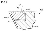
- FIG. 1 is a partial cross-sectional view showing an example of the configuration of a cutting tool according to the present embodiment.
- FIG. 2 is a TEM image (bright-field image) of 2 million times showing the interface between cubic boron nitride and the coating in FIG.
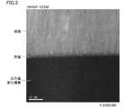
- FIG. 2 is a 2 million times TEM image (HAADF image (high-angle annular dark field image)) showing the interface between the cubic boron nitride and the coating in FIG.
- HAADF image high-angle annular dark field image
- the present disclosure provides a surface-coated cubic boron nitride sintered body excellent in peeling resistance of a coating and a cutting tool including the same.
- M to N means the upper and lower limits of the range (that is, not less than M and not more than N), and there is no unit in M, but only in N.
- the unit of M and the unit of N are the same.
- a surface-coated cubic boron nitride sintered body includes a base material that is a cubic boron nitride sintered body and a coating that covers the base material in contact with the base material.
- the Fe content is 1 at% or less
- the W content is 1 at% or less
- the O content is 2 at% or less.
- the cubic boron nitride sintered body as a base material is composed of cubic boron nitride and a binder.
- the adhesion between the substrate and the coating is affected by the difference in lattice constant between the cubic boron nitride crystal and the coating crystal in the substrate.
- the lattice constant of the crystal of the coating is larger than the lattice constant of the cubic boron nitride crystal.
- at least one of Fe and W is present at the interface, it penetrates into the crystal of the film, and increases the lattice constant of the crystal.
- Fe is often contained in a jig used when forming a film, and tends to adhere to the surface of the substrate.
- the base material is brazed to a cemented carbide obtained by sintering WC powder. Therefore, when a film is formed on the surface of the substrate after being brazed to the cemented carbide, W contained in the cemented carbide tends to adhere to the surface of the substrate.
- the lattice constant of the crystal increases due to the entry of Fe or W into the crystal of the coating, and the adhesion between the substrate and the coating tends to decrease.
- the adhesion between the cubic boron nitride and the coating is improved, and a surface-coated cubic boron nitride sintered body having improved peeling resistance of the coating can be realized.
- the thickness of the layer having a total content of Fe content and W content of 0.05 at% or more is 5 nm or less.
- the coating is a polycrystalline body.
- a region within 10 nm from the interface in the coating consists of crystal grains having an average grain size of 10 nm or less.
- region in a film increases, the stress which arises in an interface can be relieve
- the increase in grain boundaries enhances the action of preventing the plastic deformation and the progress of cracks at the grain boundaries. Further, even when subjected to an impact, the coating is difficult to peel off, and the impact resistance of the surface-coated cubic boron nitride sintered body is improved.
- the Ar content at the interface is 1 at% or less.
- a cleaning process is performed by irradiating the surface of the substrate with Ar ions.
- Ar may adhere to the surface of the substrate and remain at the interface between the substrate and the coating.
- the crystallinity of the coating is deteriorated and the stress at the interface is increased, whereby the adhesion between the substrate and the coating is lowered.
- Ar content in an interface is 1 at% or less, the adhesiveness of a base material and a film improves.
- the thickness of the coating is not less than 0.3 ⁇ m and not more than 10 ⁇ m.
- the coating is at least one element selected from the group consisting of Al, Ti, Cr and Si, and at least selected from the group consisting of C and N It contains at least one compound composed of one element. Thereby, the hardness, abrasion resistance, and oxidation resistance of the coating are improved.
- a cutting tool according to the present disclosure includes the surface-coated cubic boron nitride sintered body. According to the said cutting tool, the peeling resistance of a film improves. Thereby, the lifetime of the cutting tool can be prolonged.
- the present embodiment an embodiment of the present invention (hereinafter referred to as “the present embodiment”) will be described. However, this embodiment is not limited to these.
- the same reference numerals represent the same or corresponding parts.
- the atomic ratio when a compound or the like is represented by a chemical formula, when the atomic ratio is not particularly limited, it includes any conventionally known atomic ratio, and is not necessarily limited to a stoichiometric range.
- FIG. 1 is a partial cross-sectional view showing an example of the configuration of a cutting tool according to the present embodiment.
- the cutting tool 100 includes a base metal 101 and a surface-coated cBN sintered body 10 fixed to a predetermined region of the base metal 101 via a brazing layer 102.
- the shape and application of the cutting tool 100 are not particularly limited.
- a pin for pin milling of a shaft can be exemplified.
- the shape and material of the base metal 101 are not particularly limited, and conventionally known ones can be used.
- the base metal 101 is a cemented carbide obtained by mixing and sintering WC (tungsten carbide) and a binder (for example, Co).
- the surface-coated cBN sintered body 10 includes a base material 11 and a coating 12 that contacts the base material 11 and covers the base material 11.
- the base material 11 is fixed to the base metal 101 via the brazing layer 102.
- the material for the brazing layer (the brazing material) may be appropriately selected in consideration of the bonding strength and the melting point, and a material having a melting point of 800 ° C. or higher (for example, a material mainly composed of Ag) is preferable.
- the coating 12 covers the surface of the base material 11 and extends to the surface of the base metal 101, and constitutes a rake face 100 a and a flank face 100 b of the cutting tool 100.
- the coating 12 preferably covers the entire surface of the substrate 11, but even if a part of the substrate 11 is not covered with the coating 12 or the configuration of the coating 12 is partially different. It does not depart from the scope of the present invention.
- the base material 11 is a cBN sintered body containing cBN and a binder.
- the cBN sintered body may contain other components as long as it contains cBN and a binder, and may contain unavoidable impurities due to raw materials used, production conditions, and the like.
- the cBN is contained in the cBN sintered body, for example, 40 to 75% by volume.
- the binding material is not particularly limited as long as it exhibits an action of binding cBNs to each other, and any conventionally known binding material can be adopted.
- the binding material includes a group 4 element (Ti, Zr, Hf, etc.), a group 5 element (V, Nb, Ta, etc.) and a group 6 element (Cr, Mo, W, etc.) of the periodic table of elements.
- a compound containing at least one of these elements and at least one element of C, N, B, and O, a solid solution of such a compound, or an aluminum compound is preferable.
- the binding material may include two or more of the above compounds, solid solutions of the above compounds, and aluminum compounds.
- the coating 12 is a polycrystal.
- the coating 12 is formed by a physical vapor deposition method directly on the substrate 11 and covers the substrate 11 in contact with the substrate 11.
- the film 12 is, for example, at least one compound selected from at least one element selected from the group consisting of Al, Ti, Cr and Si and at least one element selected from the group consisting of C and N including. Examples of the compound include TiAlN, AlCrN, TiAlSiN, TiSiN, TiCN and the like.
- the thickness of the coating 12 is preferably 0.3 to 10 ⁇ m. Thereby, the effect by a film can be exhibited notably. Such effects include improvements in hardness, wear resistance, oxidation resistance, reaction resistance, and chipping resistance. If the thickness of the coating 12 is less than 0.3 ⁇ m, these effects may not be sufficiently exhibited. If the thickness exceeds 10 ⁇ m, chipping tends to occur due to residual stress in the coating 12.
- the lower limit of the thickness of the film 12 is more preferably 0.5 ⁇ m, and even more preferably 1 ⁇ m.
- the upper limit of the thickness of the film 12 is more preferably 8 ⁇ m, still more preferably 6 ⁇ m, and particularly preferably 4 ⁇ m.
- a thin film of one layer or two or more layers may be formed on the surface of the film 12 as the second film.
- examples of such a thin film include a film having a material of any one of nitrides, carbides, carbonitrides and oxides of group 4 elements.
- the Fe content and W content are subjected to structural observation and elemental analysis of the fracture surface of the surface-coated cBN sintered body 10 using an energy dispersive X-ray analyzer (EDS) attached to a transmission electron microscope (TEM). Is measured. Specifically, a line crossing the interface is specified along the normal direction of the interface between the cubic boron nitride and the coating 12 in the base material 11 in the TEM image, and along the line using EDS. Line scan measurement to measure the concentration distribution change of the selected element.
- the interface between the cubic boron nitride and the coating 12 is a position where the concentration of B contained in the cubic boron nitride is 1 ⁇ 2 of the average value in the substrate 11.
- Fe and W are metallic elements (foreign metal elements) not included in the elements constituting the cubic boron nitride and the coating 12, and when detected at the interface, they are concentrated near the interface. A large amount of Fe is contained in a jig used when the coating 12 is formed. W is included in the base metal 101 when the base metal 101 is made of a cemented carbide containing WC. Therefore, Fe released from the jig and W released from the base metal 101 adhere to the surface of the base material 11 and are likely to remain at the interface between the base material 11 and the coating 12.
- a peak occurs in the concentration distribution of Fe obtained by line scan measurement.
- the peak includes a point corresponding to the interface on the line.
- the maximum concentration (at%) of the peak is the Fe content at the interface.
- the content of W at the interface is determined by the same method.
- the Fe content at the interface is more preferably 0.5 at% or less, and further preferably 0.3 at% or less.
- the W content at the interface is more preferably 0.5 at% or less, and further preferably 0.3 at% or less.
- the lower limit of the content of Fe and W at the interface is not particularly limited, and is ideally 0 at%.
- the oxygen (O) content (at%) at the interface between the cubic boron nitride and the coating 12 in the substrate 11 is 2 at% or less.
- the O content at the interface is measured by the same method as for Fe and W. However, when O is not concentrated near the interface, no peak occurs in the O concentration distribution obtained by EDS line scan measurement. In this case, the average value of the O content (at%) in the total 4 nm section of 2 nm from the interface to the film 12 side and 2 nm to the cubic boron nitride side is obtained as the O content of the interface.
- O at the interface between cubic boron nitride and coating 12 exists as an oxide. Such an oxide reduces the adhesion between the cubic boron nitride and the coating 12.
- O content (at%) at the interface between the cubic boron nitride and the coating 12 as described above, the adhesion between the cubic boron nitride and the coating 12 is reduced due to the oxide at the interface. And the peel resistance of the coating 12 can be improved.
- the O content at the interface is more preferably 1 at% or less, still more preferably 0.5 at% or less, and particularly preferably 0.3 at% or less.
- the lower limit of the O content (at%) at the interface is not particularly limited, but is preferably less than the detection limit of EDS, and ideally 0 at%.
- the thickness of the layer (hereinafter also referred to as “different metal element layer”) having a total content of Fe content and W content of 0.05 at% or more is preferably 5 nm or less.
- the thickness of the different metal element layer is determined based on the analysis result using the EDS attached to the TEM described above. Specifically, in the synthetic data of the concentration distribution of Fe and W obtained by the EDS line scan measurement, the line length at which the total content is 0.05 at% or more is obtained as the thickness of the different metal element layer. .
- the thickness of the different metal element layer is 5 nm or less, a decrease in adhesion due to at least one of Fe and W can be suppressed, and the adhesion between the cubic boron nitride and the coating 12 is further improved.
- the thickness of the different metal element layer is more preferably 3 nm or less, still more preferably 2 nm or less, and particularly preferably 1 nm or less.
- the lower limit of the thickness of the different metal element layer is not particularly limited, and is ideally 0 nm.
- the Ar content at the interface between the cubic boron nitride and the coating 12 is preferably 1 at% or less, more preferably 0.5 at% or less, and further preferably 0.3 at% or less.
- the surface of the base material 11 is usually irradiated with Ar ions for cleaning. Therefore, Ar ions are likely to adhere to the surface of the substrate 11 and remain at the interface between the cubic boron nitride and the coating 12.
- the Ar ions remaining at the interface also deteriorate the crystallinity of the interface in the coating film and increase the stress, so that the adhesion between the cubic boron nitride and the coating film 12 tends to decrease.
- the adhesiveness between the cubic boron nitride and the coating 12 can be further improved by defining the Ar content at the interface as described above. Similar to Fe and W, the Ar content (at%) at the interface is obtained by analysis using EDS attached to TEM.
- the lower limit of the Ar content at the interface is not particularly limited, and is ideally 0 at%.
- the region within 10 nm from the interface in the coating 12 is preferably composed of crystal grains having an average grain size of 10 nm or less. Thereby, a grain boundary increases in the vicinity of the interface in the coating 12. As a result, the stress generated from the difference in lattice constant between the cubic boron nitride crystal constituting the base material 11 and the crystal constituting the coating film 12 is easily relaxed by the grain boundary, and the peeling resistance of the coating film 12 is further improved. it can. In addition, the increase in grain boundaries enhances the action of preventing the plastic deformation and the progress of cracks at the grain boundaries.
- the average grain size of the crystal grains in a region within 10 nm from the interface in the coating 12 is more preferably 5 nm or less, and even more preferably 3 nm or less.
- the average particle size is preferably 1 nm or more in consideration of crystallinity.
- the manufacturing method of the cutting tool of the present embodiment includes, for example, a step of preparing a base material (hereinafter referred to as “base material preparation step”), a step of cleaning the surface of the base material (hereinafter referred to as “bombarding step”), And a step of forming a film on the surface of the substrate (hereinafter referred to as “film formation step”). Furthermore, the manufacturing method of a cutting tool is provided with the 1st pre-processing process implemented before a bombarding process, and the 2nd pre-processing process implemented before a film-forming process. Hereinafter, each process is explained in full detail.
- Base material preparation process the base material which is a cBN sintered compact is produced using a well-known method.
- a base material is produced by sintering a mixture of cBN particles and raw material powder of a binder under high temperature and high pressure.
- the cutting tool (however, it does not have a film) whose cutting-blade part consists of a base material is obtained.
- First pretreatment process The joined body of the base metal and the base material obtained in the base material preparation step is installed in a chamber of a PVD (Physical Vapor Deposition) apparatus, and the inside of the chamber is evacuated to a vacuum by a vacuum pump. At this time, it is preferable to heat the substrate to, for example, 650 ° C. in order to reduce the influence of outgas (outgas) in the chamber.
- PVD Physical Vapor Deposition
- the pressure in the chamber is reduced to 1 ⁇ 10 ⁇ 3 Pa or less, preferably 5 ⁇ 10 ⁇ 4 Pa or less.
- the moisture pressure in the chamber is measured when the chamber is depressurized.
- the moisture pressure in the chamber is more preferably 1 ⁇ 10 ⁇ 4 Pa or less, and further preferably 5 ⁇ 10 ⁇ 5 Pa or less.
- the lower limit of the moisture pressure in the chamber is not particularly limited, but can be easily lowered to about 1 ⁇ 10 ⁇ 5 Pa by using a vacuum pump.
- a gas purification device may be connected to the chamber, and the moisture pressure in the chamber may be controlled in combination with a vacuum pump.
- the gas purification device is a device that removes water using a catalyst or an adsorbent. By using the gas purifier, the water pressure in the chamber can be easily lowered to about 1 ⁇ 10 ⁇ 6 Pa.
- An inert gas is introduced into a chamber whose moisture pressure is limited to 1 ⁇ 10 ⁇ 3 Pa or less, a bias voltage is applied to the substrate, and the surface of the substrate is irradiated with inert gas ions. Thereby, impurities such as oxides are removed from the surface of the substrate, and the surface of the substrate is cleaned.
- Ar ions can be used as the inert gas ions.
- the substrate is irradiated with inert gas ions until the water pressure in the chamber becomes 5 ⁇ 10 ⁇ 3 Pa or less (preferably 3 ⁇ 10 ⁇ 3 Pa or less).
- the moisture pressure in the chamber is measured in a state where an inert gas is contained in the chamber.
- the moisture pressure in the chamber is more preferably 5 ⁇ 10 ⁇ 4 Pa or less, and further preferably 2 ⁇ 10 ⁇ 4 Pa or less.
- the bias voltage applied to the substrate is -100 to -300V.
- a high bias voltage condition for example, ⁇ 500 V
- the inert gas ions collide with the base metal and various jigs in the chamber.
- Metal particles for example, Fe, W
- a phenomenon resputtering
- the absolute value of the bias voltage to 300 V or less as described above, it is possible to suppress the metal particles released from the base metal and the jig from adhering to the substrate surface. Furthermore, it can suppress that an inert gas ion remains on the base-material surface.
- the irradiation energy to the base material of an inert gas ion reduces by making the absolute value of a bias voltage 300V or less, since the moisture pressure in a chamber is maintained in the low state as mentioned above, Oxidation on the surface of cubic boron nitride can be sufficiently suppressed.
- the absolute value of the bias voltage is set to 100V or more.
- the inert gas in the chamber is 0.6-1 Pa. Thereby, it can suppress that an inert gas ion remains on the base-material surface.
- Second pretreatment process >> Next, the inert gas is exhausted from the chamber by operating the vacuum pump. Thereafter, the process waits until the water pressure in the chamber becomes 2 ⁇ 10 ⁇ 4 Pa or less, preferably 1 ⁇ 10 ⁇ 4 Pa. At this time, the substrate is heated to 500 ° C. or higher.
- the moisture pressure in the chamber is more preferably 3 ⁇ 10 ⁇ 5 or less, and further preferably 2 ⁇ 10 ⁇ 5 or less.
- ⁇ Film formation process After the moisture pressure in the chamber becomes 2 ⁇ 10 ⁇ 4 Pa or less, a film is formed on the substrate surface by physical vapor deposition. Any conventionally known method (such as an arc ion plating method or a sputtering method) can be employed as the physical vapor deposition method.
- a film in the arc ion plating method, can be formed using a target (metal evaporation source) containing a metal species that constitutes the film and a reactive gas such as CH 4 or N 2 .
- a target metal evaporation source
- a reactive gas such as CH 4 or N 2 .
- a film can be formed by using a target including a metal species constituting the film, a reactive gas such as CH 4 or N 2, and a sputtering gas such as Ar, Kr, or Xe.
- a target including a metal species constituting the film, a reactive gas such as CH 4 or N 2, and a sputtering gas such as Ar, Kr, or Xe.
- a sputtering gas such as Ar, Kr, or Xe.
- HiPIMS method high power ion pulse magnetron sputtering method
- the metal atoms, O, and inert gas ions contained in the jig or base metal on the substrate surface are suppressed from adhering to the substrate surface.
- the content of these atoms at the interface can be reduced.
- nucleation and grain growth occur uniformly during film formation, the grain boundary near the interface in the coating increases, and the stress generated at the interface can be relaxed. As a result, the adhesion between the cubic boron nitride and the coating is improved, and the peeling resistance of the coating is improved.
- the cutting tools 1 to 9 and 12 to 15 include the above-described surface-coated cBN sintered body.
- the cutting tools 10 and 11 are comparative examples.
- Example No. 1 cutting tool> A mixture of 70% by volume of cBN and the remaining binder (TiN, Ti, Al) was sintered at 1400 ° C. and 5 Pa to prepare a base material that was a cBN sintered body. This sintered body was bonded to a base metal made of a WC-based cemented carbide and formed into the shape of ISO standard DNGA150408. For joining, a brazing material containing Ag as a main component was used.
- the joined body of the base material and the base metal was installed in the chamber of the PVD apparatus using the HiPIMS method.
- a vacuum pump is connected to the chamber of the PVD apparatus, and the inside of the chamber can be evacuated.
- a turntable is installed in the chamber, and the turntable is configured so that a joined body including a base material can be set via a jig.
- the base material set in the chamber can be heated by a heater installed in the chamber.
- a gas pipe for introducing gas used in the bombarding process and the film forming process is connected to the chamber via a mass flow controller (MFC) for flow rate control.
- MFC mass flow controller
- a tungsten filament for generating Ar ions for the bombarding process and a sputtering source for the film forming process to which a necessary power source is connected are arranged.
- An evaporation source material (target) necessary for film formation can be set in the sputtering source.
- the substrate While evacuating the inside of the chamber with a vacuum pump, the substrate was heated at 650 ° C. for 2 hours with a heater installed in the chamber. Thereafter, heating and evacuation were continued until the water pressure in the chamber became 1 ⁇ 10 ⁇ 3 Pa or less.
- the moisture pressure in the chamber was measured using a gas analyzer “Qulee CGM-052” manufactured by ULVAC, Inc.
- the water pressure in the chamber was measured, and the bombardment was continued until the water pressure became 5 ⁇ 10 ⁇ 3 Pa or less.
- the water pressure at the end of the bombardment was 4.92 ⁇ 10 ⁇ 3 Pa.
- the moisture pressure in the bombardment was measured with Ar gas in the chamber.
- water pressure at the start of film formation was 1.94 ⁇ 10 ⁇ 4 Pa.
- Sample No. 1 was used except that an arc ion plating method was used for forming the coating and the film forming process was performed according to the following film forming conditions. Sample No. 1 under the same conditions as in No. 1. 14 cutting tools were produced.
- Sample No. For each of the cutting tools 1 to 15, samples for analysis were prepared that were broken in the direction perpendicular to the interface between the substrate and the coating. The fracture surface is smoothed by irradiation with a focused ion beam, and then analyzed by an ion milling apparatus using an Ar ion beam so that the thickness along the normal direction of the fracture surface is 100 nm. The fracture surface of the sample was polished. This is to suppress variation in the measured value of the O content due to the thickness of the analytical sample.
- the sample was introduced into a TEM apparatus to obtain a TEM image near the interface between the cubic boron nitride and the coating, Line scan measurement by EDS was performed so as to cross the interface with the coating. The following was used as an analyzer.
- a 200 nm long line is specified that crosses the interface along the normal direction of the interface between the cubic boron nitride and the coating, and the concentration distribution of elements along the line is determined using EDS.
- a line scan measurement was performed to measure the change.
- the measurement elements were Fe, W, O, and Ar in addition to B and N, which are calibration elements of cubic boron nitride, and the constituent elements of the film.
- B and N which are calibration elements of cubic boron nitride, and the constituent elements of the film.
- concentration in a base material was specified as a point on an interface.
- the concentrations of elements other than B and N detected in cubic boron nitride are the background level (detection limit) in the measurement, and the respective concentrations of these elements in cubic boron nitride.
- the average values of these were calculated, these values were excluded from the line scan measurement results, and the concentrations of the measured elements were recalculated.
- the maximum concentration of Fe and W concentration distribution peaks (peaks including points on the interface) in the vicinity of the interface in the recalculated line scan measurement results was defined as the Fe (W) content (at%) at the interface.
- Sample No. In 1 to 15 cutting tools, at least one of Fe and W was detected at the interface.
- the O content (at%) at the interface was evaluated from the line scan measurement result using EDS.
- the maximum concentration of the peak was defined as the O content (at%) at the interface, similarly to Fe and W.
- the average of the O content (at%) in the total 4 nm section of 2 nm from the interface to the film side and 2 nm to the cubic boron nitride side was defined as the O content (at%) at the interface.
- ⁇ Average particle size of the coating near the interface> In a 5 million times TEM image, the average grain size of the crystal grains at a position of 10 nm from the interface in the coating was measured. Specifically, a lattice image is taken in a high-resolution TEM image, crystal grains are distinguished by the difference in crystal orientation and the presence of grain boundaries, the width of 30 crystal grains is measured for one sample, and the average value is calculated. The average particle size was taken.
- the cutting edge portion was cut out by wire electric discharge machining, and the cut out portion was embedded in resin. Thereafter, the cross section of the coating was exposed by CP (cross section polisher) processing based on the ion milling method, and an SEM image at a magnification of 15000 was observed. The film thickness was measured at five points in a region within 1 mm from the tip of the blade edge, and an average value was taken.
- Table 2 shows Sample No. For each of the cutting tools 1 to 15, the content at the interface of Fe and W, the content of O and Ar at the interface, the thickness of the different metal element layer, and the average particle diameter at a position 10 nm from the interface in the coating film The measurement result of the thickness of a film and a tool life is shown.
- FIG. 2 shows sample no. 2 is a TEM image (bright-field image) of 2 million times showing the interface between cubic boron nitride and the coating in FIG.
- FIG. 2 is a 2 million times TEM image (HAADF image (high-angle annular dark field image)) showing the interface between the cubic boron nitride and the coating in FIG.
- HAADF image high-angle annular dark field image
- the Fe content at the interface is 1 at% or less and the W content is 1 at% or less, it is possible to suppress an increase in the lattice constant of the crystal in the coating film due to Fe and W entering the crystal of the coating film.
- an increase in the difference in lattice constant between the cubic boron nitride crystal and the coating crystal in the substrate can be suppressed, and the adhesion between the cubic boron nitride and the coating is improved.
- the O content at the interface between the cubic boron nitride and the coating is suppressed to 2 at% or less, and the decrease in adhesion between the cubic boron nitride and the coating due to O can be suppressed.
- the adhesion between the cubic boron nitride and the coating is improved. It is considered that the peel resistance of the coating in the cutting tools 1 to 9 and 12 to 15 was improved.
- sample no. With 10 cutting tools, it was confirmed that the tool life was as short as 2 minutes.
- Sample No. 10 the moisture pressure before the start of bombardment is 1.98 ⁇ 10 ⁇ 3 Pa, and the moisture pressure at the end of bombardment is 7.93 ⁇ 10 ⁇ 3 Pa. Therefore, at the interface between the cubic boron nitride and the coating, The O content (at%) is higher than 2 at%. As a result, it is considered that the adhesion between the cubic boron nitride and the coating is lowered, and the tool life is shortened.
Landscapes
- Engineering & Computer Science (AREA)
- Chemical & Material Sciences (AREA)
- Mechanical Engineering (AREA)
- Ceramic Engineering (AREA)
- Materials Engineering (AREA)
- Structural Engineering (AREA)
- Organic Chemistry (AREA)
- Inorganic Chemistry (AREA)
- Crystallography & Structural Chemistry (AREA)
- Manufacturing & Machinery (AREA)
- Physical Vapour Deposition (AREA)
- Cutting Tools, Boring Holders, And Turrets (AREA)
Abstract
表面被覆立方晶窒化硼素焼結体は、立方晶窒化硼素焼結体である基材と、基材に接して基材を被覆する被膜とを備える。基材中の立方晶窒化硼素と被膜との界面において、Fe含有量は1at%以下であり、W含有量は1at%以下であり、かつO含有量は2at%以下である。
Description
本発明は、表面被覆立方晶窒化硼素焼結体およびこれを備える切削工具に関する。本出願は、2017年5月29日に出願した日本特許出願である特願2017-105583号に基づく優先権を主張する。当該日本特許出願に記載された全ての記載内容は、参照によって本明細書に援用される。
従来、立方晶窒化硼素(以下、「cBN」ともいう。)焼結体を用いた切削工具が知られている。たとえば、特開2015-209354号公報(特許文献1)には、cBN焼結体にバイアス電圧を印加し、ArイオンによりcBN焼結体の表面に対してエッチングを行なった後に、当該表面に被膜を形成することにより切削工具を製造する技術が開示されている。
本開示の一態様に係る表面被覆立方晶窒化硼素焼結体は、立方晶窒化硼素焼結体である基材と、基材に接して基材を被覆する被膜とを備える。基材中の立方晶窒化硼素と被膜との界面において、Fe含有量は1at%以下であり、W含有量は1at%以下であり、かつO含有量は2at%以下である。
[本開示が解決しようとする課題]
ところで近年、切削速度の高速化および難削材に対する切削性能の向上の要求が高まっている。しかしながら、従来の切削工具では、切削速度を速めた場合または難削材を切削するときに被膜が剥離しやすく、上記の要求を十分に満たすことができない。
ところで近年、切削速度の高速化および難削材に対する切削性能の向上の要求が高まっている。しかしながら、従来の切削工具では、切削速度を速めた場合または難削材を切削するときに被膜が剥離しやすく、上記の要求を十分に満たすことができない。
以上の点に鑑み、本開示では、被膜の耐剥離性に優れた表面被覆立方晶窒化硼素焼結体およびこれを備える切削工具を提供する。
[本開示の効果]
上記によれば、被膜の耐剥離性に優れた表面被覆立方晶窒化硼素焼結体および切削工具を提供することができる。
上記によれば、被膜の耐剥離性に優れた表面被覆立方晶窒化硼素焼結体および切削工具を提供することができる。
[本願発明の実施形態の説明]
最初に本開示の実施態様を列記して説明する。なお、本明細書において「M~N」という形式の表記は、範囲の上限下限(すなわちM以上N以下)を意味し、Mにおいて単位の記載がなく、Nにおいてのみ単位が記載されている場合、Mの単位とNの単位とは同じである。
最初に本開示の実施態様を列記して説明する。なお、本明細書において「M~N」という形式の表記は、範囲の上限下限(すなわちM以上N以下)を意味し、Mにおいて単位の記載がなく、Nにおいてのみ単位が記載されている場合、Mの単位とNの単位とは同じである。
〔1〕本開示に係る表面被覆立方晶窒化硼素焼結体は、立方晶窒化硼素焼結体である基材と、基材に接して基材を被覆する被膜とを備える。基材中の立方晶窒化硼素と被膜との界面において、Fe含有量は1at%以下であり、W含有量は1at%以下であり、かつO含有量は2at%以下である。
基材である立方晶窒化硼素焼結体は、立方晶窒化硼素と結合剤とからなる。基材と被膜との密着性は、基材中の立方晶窒化硼素の結晶と被膜の結晶との格子定数の差に影響される。一般に、被膜の結晶の格子定数は、立方晶窒化硼素の結晶の格子定数よりも大きい。ここで、FeおよびWの少なくとも一方は、界面に存在すると、被膜の結晶中に入り込み、当該結晶の格子定数を増大させる。その結果、立方晶窒化硼素の結晶と被膜の結晶との格子定数の差がさらに大きくなり、基材と被膜との密着性が低下する。しかしながら、上記の構成によれば、立方晶窒化硼素の結晶と被膜の結晶との格子定数の差に起因する密着性の低下を抑制できる。
Feは、被膜を形成する際に用いる治具に含まれることが多く、基材の表面に付着しやすい。また、基材は、WC粉末を焼結させた超硬合金にろう付けされて使用されることが多い。そのため、超硬合金にろう付けされた後に基材の表面に被膜を形成する場合に、超硬合金に含まれるWが基材の表面に付着しやすい。FeまたはWが基材と被膜との界面に存在すると、FeまたはWが被膜の結晶中に入り込むことによって、当該結晶の格子定数が大きくなり、基材と被膜との密着性が低下しやすい。しかしながら、上記の構成によれば、基材中の立方晶窒化硼素の結晶と被膜の結晶との格子定数の差に起因する密着性の低下を抑制できる。
また、立方晶窒化硼素と被膜との界面に酸化物が存在すると、立方晶窒化硼素と被膜との密着性が低下しやすい。しかしながら、上記の構成によれば、酸化物による立方晶窒化硼素と被膜との密着性の低下を抑制できる。
以上により、立方晶窒化硼素と被膜との密着性が向上し、被膜の耐剥離性が向上した表面被覆立方晶窒化硼素焼結体を実現できる。
〔2〕Fe含有量とW含有量との合計含有量が0.05at%以上である層の厚みは5nm以下である。これにより、FeおよびWの少なくとも一方に起因した密着性の低下を抑制でき、基材と被膜との密着性がさらに向上する。
〔3〕上記表面被覆立方晶窒化硼素焼結体において、被膜は多結晶体である。被膜における界面から10nm以内の領域は、平均粒径が10nm以下の結晶粒からなる。これにより、被膜における界面近傍領域の粒界が増加し、界面に生じる応力を緩和させることができ、被膜の耐剥離性がさらに向上する。また、粒界が増加することにより、粒界において塑性変形および亀裂の進展を阻止する作用が高められる。さらに、衝撃を受けた場合であっても、被膜が剥離しにくくなり、表面被覆立方晶窒化硼素焼結体の耐衝撃性が向上する。
〔4〕上記界面におけるAr含有量は1at%以下である。一般に、基材の表面にArイオンを照射して、クリーニングする処理が行なわれる。このとき、Arが基材の表面に付着し、基材と被膜との界面に残る場合がある。Arが界面に多く存在すると、被膜の結晶性が悪化するとともに、界面の応力が増大することにより、基材と被膜との密着性が低下する。しかしながら、上記の構成によれば、界面におけるAr含有量が1at%以下であるため、基材と被膜との密着性が向上する。
〔5〕上記表面被覆立方晶窒化硼素焼結体において、被膜の厚みは0.3μm以上10μm以下である。これにより、被膜による耐摩耗性の向上等の効果をより顕著に発揮することができる。
〔6〕上記表面被覆立方晶窒化硼素焼結体において、被膜は、Al,Ti,CrおよびSiからなる群より選択される少なくとも1種の元素と、CおよびNからなる群より選択される少なくとも1種の元素とからなる少なくとも1種の化合物を含む。これにより、被膜の硬度、耐摩耗性、耐酸化性が向上する。
〔7〕本開示に係る切削工具は、上記表面被覆立方晶窒化硼素焼結体を備える。上記切削工具によれば、被膜の耐剥離性が向上する。これにより、切削工具の寿命を長期化することができる。
[本願発明の実施形態の詳細]
以下、本発明の一実施形態(以下「本実施形態」と記す)について説明する。ただし、本実施形態はこれらに限定されるものではない。なお以下の実施の形態の説明に用いられる図面において、同一の参照符号は、同一部分または相当部分を表わす。また、本明細書において化合物などを化学式で表す場合、原子比を特に限定しないときは従来公知のあらゆる原子比を含むものとし、必ずしも化学量論的範囲のものに限定されるものではない。たとえば「AlCrN」と記載されている場合、AlCrNを構成する原子数の比はAl:Cr:N=0.5:0.5:1に限られず、従来公知のあらゆる原子比が含まれる。
以下、本発明の一実施形態(以下「本実施形態」と記す)について説明する。ただし、本実施形態はこれらに限定されるものではない。なお以下の実施の形態の説明に用いられる図面において、同一の参照符号は、同一部分または相当部分を表わす。また、本明細書において化合物などを化学式で表す場合、原子比を特に限定しないときは従来公知のあらゆる原子比を含むものとし、必ずしも化学量論的範囲のものに限定されるものではない。たとえば「AlCrN」と記載されている場合、AlCrNを構成する原子数の比はAl:Cr:N=0.5:0.5:1に限られず、従来公知のあらゆる原子比が含まれる。
〈切削工具〉
図1は、本実施形態に係る切削工具の構成の一例を示す部分断面図である。図1に示されるように、切削工具100は、台金101と、台金101の所定の領域にろう付け層102を介して固定された表面被覆cBN焼結体10とを備える。
図1は、本実施形態に係る切削工具の構成の一例を示す部分断面図である。図1に示されるように、切削工具100は、台金101と、台金101の所定の領域にろう付け層102を介して固定された表面被覆cBN焼結体10とを備える。
切削工具100の形状および用途は特に制限されない。たとえばドリル、エンドミル、ドリル用刃先交換型切削チップ、エンドミル用刃先交換型切削チップ、フライス加工用刃先交換型切削チップ、旋削加工用刃先交換型切削チップ、メタルソー、歯切工具、リーマ、タップ、クランクシャフトのピンミーリング加工用チップなどを挙げることができる。
台金101の形状および材料は特に限定されず、従来公知のものを用いることができる。たとえば、台金101は、WC(炭化タングステン)と結合材(たとえば、Co)とを混合して焼結した超硬合金である。
表面被覆cBN焼結体10は、基材11と、基材11に接して基材11を被覆する被膜12とを備える。基材11は、台金101にろう付け層102を介して固定される。ろう付け層の材料(ろう材)は、接合強度や融点を考慮し適宜選択すればよく、800℃以上の融点を有する材料(たとえば、Agを主成分とする材料)が好ましい。
被膜12は、基材11の表面を被覆するとともに、台金101の表面にまで延在し、切削工具100のすくい面100aおよび逃げ面100bを構成する。なお、被膜12は、基材11の全面を被覆することが好ましいが、基材11の一部がこの被膜12で被覆されていなかったり、被膜12の構成が部分的に異なっていたりしたとしても本発明の範囲を逸脱するものではない。
《基材》
基材11は、cBNと結合材とを含むcBN焼結体である。cBN焼結体は、cBNと結合材とを含む限り他の成分を含んでもよく、また使用する原料や製造条件等に起因する不可避不純物を含み得る。cBNは、cBN焼結体にたとえば40~75体積%含まれている。
基材11は、cBNと結合材とを含むcBN焼結体である。cBN焼結体は、cBNと結合材とを含む限り他の成分を含んでもよく、また使用する原料や製造条件等に起因する不可避不純物を含み得る。cBNは、cBN焼結体にたとえば40~75体積%含まれている。
結合材は、cBN同士を互いに結合する作用を示すものであれば特に限定されず、従来公知の結合材をいずれも採用できる。結合材は、たとえば、元素の周期表の第4族元素(Ti、ZrまたはHf等)、第5族元素(V、NbまたはTa等)および第6族元素(Cr、MoまたはW等)のうちの少なくとも1つの元素と、C、N、B及びOのうちの少なくとも1つの元素とを含む化合物、かかる化合物の固溶体、または、アルミニウム化合物であることが好ましい。結合材は、上記化合物、上記化合物の固溶体、および、アルミニウム化合物のうちの2種以上を含んでもよい。
《被膜》
被膜12は、多結晶体である。被膜12は、基材11の直上に物理蒸着法により形成され、基材11と接して基材11を被覆する。被膜12は、たとえば、Al、Ti、CrおよびSiからなる群より選択される少なくとも1種の元素と、CおよびNからなる群より選択される少なくとも1種の元素とからなる少なくとも1種の化合物を含む。当該化合物としては、たとえばTiAlN、AlCrN、TiAlSiN、TiSiN、TiCN等を挙げることができる。被膜12としてこのような化合物を選択することにより、被膜12の硬度が向上するとともに、耐摩耗性および耐酸化性が向上する。被膜12の耐摩耗性が向上することに伴い、切削抵抗が増大しにくく、摩耗が発達しにくくなる。
被膜12は、多結晶体である。被膜12は、基材11の直上に物理蒸着法により形成され、基材11と接して基材11を被覆する。被膜12は、たとえば、Al、Ti、CrおよびSiからなる群より選択される少なくとも1種の元素と、CおよびNからなる群より選択される少なくとも1種の元素とからなる少なくとも1種の化合物を含む。当該化合物としては、たとえばTiAlN、AlCrN、TiAlSiN、TiSiN、TiCN等を挙げることができる。被膜12としてこのような化合物を選択することにより、被膜12の硬度が向上するとともに、耐摩耗性および耐酸化性が向上する。被膜12の耐摩耗性が向上することに伴い、切削抵抗が増大しにくく、摩耗が発達しにくくなる。
被膜12の厚みは、0.3~10μmであることが好ましい。これにより、被膜による効果を顕著に発揮することができる。当該効果には、硬度、耐摩耗性、耐酸化性、耐反応性、耐チッピング性の向上が含まれる。被膜12の厚みが0.3μm未満であると、これらの効果が十分に発揮されない場合があり、10μmを超えると、被膜12における残留応力のためにチッピングが生じやすくなる。被膜12の厚みの下限は、より好ましくは0.5μmであり、さらに好ましくは1μmである。被膜12の厚みの上限は、より好ましくは8μmであり、さらに好ましくは6μmであり、特に好ましくは4μmである。
なお、被膜12の表面上に、第2被膜として、1層または2層以上の薄膜が形成されてもよい。このような薄膜としては、たとえば4族元素の窒化物、炭化物、炭窒化物および酸化物のいずれかの材質を有する膜等が挙げられる。
《立方晶窒化硼素と被膜との界面》
基材11と被膜12との界面のうち、立方晶窒化硼素と被膜12の界面において、Fe含有量は1at%以下であり、W含有量は1at%以下であり、かつO含有量は2at%以下である。
基材11と被膜12との界面のうち、立方晶窒化硼素と被膜12の界面において、Fe含有量は1at%以下であり、W含有量は1at%以下であり、かつO含有量は2at%以下である。
Fe含有量およびW含有量は、透過型電子顕微鏡(TEM)付帯のエネルギー分散型X線分析器(EDS)を用いて、表面被覆cBN焼結体10の破断面の組織観察および元素分析を行なうことにより測定される。具体的には、TEM像にて基材11中の立方晶窒化硼素と被膜12との界面の法線方向に沿って当該界面を横断するラインを指定し、EDSを用いて、当該ラインに沿った元素の濃度分布変化を計測するラインスキャン測定を行なう。ここで、立方晶窒化硼素と被膜12との界面は、立方晶窒化硼素に含まれるBの濃度が基材11中の濃度の平均値の1/2となる位置である。
FeおよびWは、立方晶窒化硼素および被膜12を構成する元素に含まれない金属元素(異金属元素)であり、界面において検出される場合には界面付近に集中して存在することになる。Feは、被膜12を形成する際に用いられる治具に多く含まれている。Wは、WCを含む超硬合金によって台金101を構成した場合に、当該台金101に含まれる。そのため、治具から放出されたFeおよび台金101から放出されたWが基材11の表面に付着し、基材11と被膜12との界面に残存しやすい。
Feが界面付近に集中して存在すると、ラインスキャン測定によって得られたFeの濃度分布においてピークが生じる。当該ピークは、ライン上の界面に対応する点を含む。ここでは、当該ピークの最大濃度(at%)を、界面におけるFeの含有量とする。同様の方法により、界面におけるWの含有量が求められる。
FeおよびWの少なくとも一方は、界面付近に存在する場合、被膜12の結晶に入り込み、被膜12を構成する結晶の格子定数を増大させる。これにより、基材11を構成する立方晶窒化硼素の結晶の格子定数と被膜12を構成する結晶の格子定数との差が大きくなり、立方晶窒化硼素と被膜12との密着性を低下させる。しかしながら、界面におけるFeおよびWの含有量を上記のように規定することにより、FeまたはWに起因した立方晶窒化硼素と被膜12との密着性の低下を抑制し、被膜12の耐剥離性を向上させることができる。
界面におけるFe含有量は、より好ましくは0.5at%以下であり、さらに好ましくは0.3at%以下である。界面におけるW含有量は、より好ましくは0.5at%以下であり、さらに好ましくは0.3at%以下である。界面におけるFeおよびWの含有量の下限は、特に限定されるものではなく、理想的には0at%である。
基材11中の立方晶窒化硼素と被膜12との界面における酸素(O)含有量(at%)は、2at%以下である。界面におけるO含有量は、FeおよびWと同様の方法により測定される。ただし、Oが界面付近に集中して存在しない場合、EDSのラインスキャン測定によって得られたO濃度分布においてピークが生じない。この場合、界面から被膜12側に2nm、立方晶窒化硼素側に2nmの合計4nmの区間のO含有量(at%)の平均値を界面のO含有量として求める。
立方晶窒化硼素と被膜12との界面におけるOの多くは酸化物として存在する。このような酸化物は、立方晶窒化硼素と被膜12との密着性を低下させる。しかしながら、立方晶窒化硼素と被膜12との界面におけるO含有量(at%)を上記のように規定することにより、界面の酸化物に起因した立方晶窒化硼素と被膜12との密着性の低下を抑制し、被膜12の耐剥離性を向上させることができる。
界面におけるO含有量は、より好ましくは1at%以下であり、さらに好ましくは0.5at%以下であり、特に好ましくは0.3at%以下である。界面におけるO含有量(at%)の下限は特に限定されるものではないが、EDSの検出限界未満であることが好ましく、理想的には0at%である。
Fe含有量とW含有量との合計含有量が0.05at%以上である層(以下、「異金属元素層」ともいう。)の厚みは、5nm以下であることが好ましい。異金属元素層の厚みは、上述したTEM付帯のEDSを用いた分析結果に基づいて求められる。具体的には、EDSのラインスキャン測定によって得られたFeとWとの濃度分布の合成データにおいて、合計含有量が0.05at%以上となるライン長さを、異金属元素層の厚みとして求める。異金属元素層の厚みが5nm以下であることにより、FeおよびWの少なくとも一方に起因した密着性の低下を抑制でき、立方晶窒化硼素と被膜12との密着性がさらに向上する。異金属元素層の厚みは、より好ましくは3nm以下であり、さらに好ましくは2nm以下であり、特に好ましくは1nm以下である。異金属元素層の厚みの下限は特に限定されるものではなく、理想的には0nmである。
立方晶窒化硼素と被膜12との界面におけるAr含有量は、好ましくは1at%以下であり、より好ましくは0.5at%以下であり、さらに好ましくは0.3at%以下である。基材11に被膜12を形成する前に、通常、基材11の表面にArイオンを照射してクリーニングする処理が行なわれる。そのため、Arイオンが基材11の表面に付着し、立方晶窒化硼素と被膜12との界面に残存しやすい。界面に残存するArイオンによっても、被膜における界面の結晶性が悪化するとともに、応力が増加するため、立方晶窒化硼素と被膜12との密着性が低下しやすい。そのため、界面におけるAr含有量を上記のように規定することにより、立方晶窒化硼素と被膜12との密着性をより向上させることができる。界面におけるAr含有量(at%)は、FeおよびWと同様にTEM付帯のEDSを用いた分析によって求められる。界面におけるAr含有量の下限は特に限定されるものではなく、理想的には0at%である。
被膜12における界面から10nm以内の領域は、平均粒径が10nm以下の結晶粒により構成されることが好ましい。これにより、被膜12における界面近傍には粒界が増加する。その結果、基材11を構成する立方晶窒化硼素の結晶と被膜12を構成する結晶との格子定数の差から生じた応力が粒界によって緩和されやすくなり、被膜12の耐剥離性をさらに向上できる。また、粒界が増加することにより、粒界において塑性変形および亀裂の進展を阻止する作用が高められる。さらに、衝撃を受けた場合であっても、被膜が剥離しにくくなるため、表面被覆cBN焼結体10の耐衝撃性が向上する。被膜12における界面から10nm以内の領域の結晶粒の平均粒径は、より好ましくは5nm以下であり、さらに好ましくは3nm以下である。当該平均粒径は、結晶性を考慮して、1nm以上であることが好ましい。
〈切削工具の製造方法〉
本実施形態の切削工具の製造方法は、たとえば、基材を準備する工程(以下、「基材準備工程」という)と、基材表面をクリーニングする工程(以下、「ボンバード工程」という)と、基材表面に被膜を形成する工程(以下、「成膜工程」という)とを備える。さらに、切削工具の製造方法は、ボンバード工程の前に実施される第1前処理工程と、成膜工程の前に実施される第2前処理工程とを備える。以下、各工程について詳述する。
本実施形態の切削工具の製造方法は、たとえば、基材を準備する工程(以下、「基材準備工程」という)と、基材表面をクリーニングする工程(以下、「ボンバード工程」という)と、基材表面に被膜を形成する工程(以下、「成膜工程」という)とを備える。さらに、切削工具の製造方法は、ボンバード工程の前に実施される第1前処理工程と、成膜工程の前に実施される第2前処理工程とを備える。以下、各工程について詳述する。
《基材準備工程》
まず、公知の方法を用いて、cBN焼結体である基材を作製する。たとえば、cBN粒子と結合材の原料粉末とからなる混合物を高温高圧下で焼結させることにより、基材が作製される。
まず、公知の方法を用いて、cBN焼結体である基材を作製する。たとえば、cBN粒子と結合材の原料粉末とからなる混合物を高温高圧下で焼結させることにより、基材が作製される。
次に、得られた基材を所定形状に加工した後、台金にろう付けする。これにより、切れ刃部分が基材からなる切削工具(ただし、被膜を有していない)が得られる。
《第1前処理工程》
基材準備工程によって得られた台金と基材との接合体をPVD(Physical Vapor Deposition)装置のチャンバ内に設置し、チャンバ内を真空ポンプで真空に排気する。このとき、チャンバ内のアウトガス(出ガス)による影響を低減するために、基材をたとえば650℃に加熱することが好ましい。
基材準備工程によって得られた台金と基材との接合体をPVD(Physical Vapor Deposition)装置のチャンバ内に設置し、チャンバ内を真空ポンプで真空に排気する。このとき、チャンバ内のアウトガス(出ガス)による影響を低減するために、基材をたとえば650℃に加熱することが好ましい。
チャンバに接続された真空ポンプを用いて、チャンバ内の水分圧が1×10⁻³Pa以下、好ましくは5×10⁻⁴Pa以下となるまで減圧する。チャンバ内の水分圧は、チャンバ内を減圧しているときに測定される。チャンバ内の水分圧は、より好ましくは1×10⁻⁴Pa以下であり、さらに好ましくは5×10⁻⁵Pa以下である。チャンバ内の水分圧の下限は特に限定されるものではないが、真空ポンプを用いることにより1×10⁻⁵Pa程度まで容易に下げることができる。
なお、チャンバにガス精製装置を接続し、真空ポンプと併用してチャンバ内の水分圧を制御してもよい。ガス精製装置は、触媒または吸着剤を用いて水を除去する装置である。ガス精製装置を用いることにより、チャンバ内の水分圧を1×10⁻⁶Pa程度まで容易に下げることができる。
《ボンバード工程》
水分圧が1×10⁻³Pa以下に制限されたチャンバ内に不活性ガスを導入し、基材にバイアス電圧を印加して、不活性ガスイオンを基材の表面に照射する。これにより、基材の表面から酸化物等の不純物が除去され、基材の表面がクリーニングされる。不活性ガスイオンとしては、たとえばArイオンを用いることができる。
水分圧が1×10⁻³Pa以下に制限されたチャンバ内に不活性ガスを導入し、基材にバイアス電圧を印加して、不活性ガスイオンを基材の表面に照射する。これにより、基材の表面から酸化物等の不純物が除去され、基材の表面がクリーニングされる。不活性ガスイオンとしては、たとえばArイオンを用いることができる。
このとき、チャンバ内の水分圧が5×10⁻³Pa以下(好ましくは、3×10⁻³Pa以下)になるまで、不活性ガスイオンを基材に照射する。チャンバ内の水分圧は、チャンバ内に不活性ガスが含まれる状態で測定される。チャンバ内の水分圧が低い状態になるまでボンバードを行なうことにより、立方晶窒化硼素表面の酸化膜を除去し、ボンバード中およびボンバード後に立方晶窒化硼素表面が再び酸化することを抑制することができる。チャンバ内の水分圧は、より好ましくは5×10⁻⁴Pa以下であり、さらに好ましくは2×10⁻⁴Pa以下である。
基材に印加されるバイアス電圧は-100~-300Vである。特開2015-209354号公報に記載されているような高バイアス電圧条件(たとえば、-500V)では、不活性ガスイオンが台金およびチャンバ内の各種治具に衝突することにより、台金および治具から金属粒子(たとえば、Fe、W)が放出され、基材表面に堆積する現象(再スパッタ)が生じやすい。しかしながら、上記のようにバイアス電圧の絶対値を300V以下にすることにより、台金および治具から放出された金属粒子が基材表面に付着することを抑制できる。さらに、不活性ガスイオンが基材表面に残存することを抑制することができる。
なお、バイアス電圧の絶対値を300V以下にすることにより、不活性ガスイオンの基材への照射エネルギーが減少するものの、チャンバ内の水分圧が上記のように低い状態に維持されているため、立方晶窒化硼素表面の酸化を十分に抑制することができる。
バイアス電圧の絶対値が100V未満であると、不活性ガスイオンの基材への照射エネルギーが低くなりすぎ、基材表面のクリーニングを十分に行なうことができない。そのため、バイアス電圧の絶対値は、100V以上に設定される。
チャンバ内の不活性ガスは0.6~1Paである。これにより、不活性ガスイオンが基材表面に残存することを抑制することができる。
以上のようなボンバード工程を行なうことにより、治具や台金に含まれる金属原子、O、不活性ガスイオンが基材表面へ付着することを抑制することができる。
《第2前処理工程》
次に、真空ポンプを動作させてチャンバ内から不活性ガスを排気する。その後、チャンバ内の水分圧が2×10⁻⁴Pa以下、好ましくは1×10⁻⁴Paになるまで待機する。このとき、基材を500℃以上に加熱する。チャンバ内の水分圧は、より好ましくは3×10⁻⁵以下であり、さらに好ましくは2×10⁻⁵以下である。
次に、真空ポンプを動作させてチャンバ内から不活性ガスを排気する。その後、チャンバ内の水分圧が2×10⁻⁴Pa以下、好ましくは1×10⁻⁴Paになるまで待機する。このとき、基材を500℃以上に加熱する。チャンバ内の水分圧は、より好ましくは3×10⁻⁵以下であり、さらに好ましくは2×10⁻⁵以下である。
《成膜工程》
チャンバ内の水分圧が2×10⁻⁴Pa以下になった後、物理蒸着法により基材表面に被膜を形成する。物理蒸着法としては、従来公知の方法(アークイオンプレーティング法、スパッタリング法など)をいずれも採用することができる。
チャンバ内の水分圧が2×10⁻⁴Pa以下になった後、物理蒸着法により基材表面に被膜を形成する。物理蒸着法としては、従来公知の方法(アークイオンプレーティング法、スパッタリング法など)をいずれも採用することができる。
アークイオンプレーティング法では、被膜を構成することになる金属種を含むターゲット(金属蒸発源)とCH4またはN2等の反応ガスとを用いて、被膜を形成することができる。アークイオンプレーティング法により被膜を形成する条件としては、表面被覆cBN焼結体の被膜をアークイオンプレーティング法により形成する公知の条件を採用することができる。
スパッタ法では、被膜を構成することになる金属種を含むターゲットとCH4またはN2等の反応ガスとAr、KrまたはXe等のスバッタガスとを用いて、被膜を形成することができる。スパッタ法により被覆層を形成する条件としては、表面被覆cBN焼結体の被膜をスパッタ法により形成する公知の条件を採用することができる。
スパッタ法の中でも、コンデンサによって充電した電力を瞬間的に投入して、ターゲット材を効率良くイオン化することが可能な高出力イオンパルスマグネトロンスパッタリング法(High Power Impulse Magnetron Sputtering:HiPIMS法)を用いることが好ましい。これにより、緻密な被膜を形成することができる。
上記のボンバード工程において、基材表面における治具や台金に含まれる金属原子、O、不活性ガスイオンが基材表面へ付着することを抑制しているため、立方晶窒化硼素と被膜との界面におけるこれらの原子の含有量を低減できる。また、成膜時の核発生と粒成長とが均一に起こるために、被膜における界面近傍の粒界が増加し、界面に生じる応力を緩和することができる。その結果、立方晶窒化硼素と被膜との密着性が向上し、被膜の耐剥離性が向上する。
以下実施例を挙げて本発明をより詳細に説明するが、本発明はこれらに限定されるものではない。試料No.1~9,12~15の切削工具は、上述の表面被覆cBN焼結体を備えている。試料No.10,11の切削工具は比較例である。
〈試料No.1の切削工具〉
70体積%のcBNと残部の結合材(TiN,Ti,Al)との混合物を1400℃、5Paにて焼結させ、cBN焼結体である基材を作製した。この焼結体をWC基超硬合金からなる台金に接合し、ISO規格のDNGA150408の形状に成形した。接合には、Agを主成分とするろう材を用いた。
70体積%のcBNと残部の結合材(TiN,Ti,Al)との混合物を1400℃、5Paにて焼結させ、cBN焼結体である基材を作製した。この焼結体をWC基超硬合金からなる台金に接合し、ISO規格のDNGA150408の形状に成形した。接合には、Agを主成分とするろう材を用いた。
次に、HiPIMS法を用いたPVD装置のチャンバ内に、基材と台金との接合体を設置した。
ここで、PVD装置について説明する。PVD装置のチャンバには真空ポンプが接続されており、チャンバ内を真空引き可能である。チャンバ内には、回転テーブルが設置されており、当該回転テーブルは、治具を介して基材を含む接合体がセットできるように構成されている。チャンバ内にセットされた基材は、チャンバ内に設置されているヒーターにより加熱することができる。またチャンバには、ボンバード工程および成膜工程に用いるガスを導入するためのガス配管が流量制御用のマスフローコントローラ(MFC:Mass Flow Controller)を介して接続されている。さらにチャンバ内には、ボンバード工程用のArイオンを発生させるためのタングステンフィラメント、必要な電源が接続された成膜工程用のスパッタ源が配置されている。そしてスパッタ源には、成膜に必要な蒸発源原料(ターゲット)がセット可能である。
チャンバー内を真空ポンプで真空排気しながら、チャンバ内に設置されたヒーターにより基材を650℃で2時間加熱した。その後、チャンバ内の水分圧が1×10⁻³Pa以下になるまで加熱と真空引きとを継続した。チャンバ内の水分圧は、株式会社アルバック製のガス分析器「Qulee CGM-052」を使用して測定した。
そしてチャンバ内の水分圧が1×10⁻³Pa以下になったときに、ボンバード工程を開始し、Arイオンによる基材表面のクリーニングを60分間行なった。ボンバード開始前の水分圧は0.921×10⁻³Paであった。ボンバード工程では、Arガスをチャンバ内に導入し、チャンバ内の圧力を0.8Paに維持した。このとき、基材に-150Vのバイアス電圧を印加するとともに、タングステンフィラメントに電流を流すことによって、Arガス中でグロー放電を発生させた。
ボンバード中もチャンバ内の水分圧を測定し、水分圧が5×10⁻³Pa以下になるまでボンバードを継続した。ボンバード終了時の水分圧は4.92×10⁻³Paであった。ボンバード中の水分圧は、チャンバ内にArガスが入っている状態で測定された。
その後、チャンバ内からArガスを排気し、チャンバ内の水分圧が2×10⁻⁴Pa以下になるまで待機した。このとき、基材の温度が500℃になるように温度制御した。
そして、チャンバ内の水分圧が2×10⁻⁴Pa以下になったときに、以下の成膜条件に従って、基材の表面上に被膜を形成する成膜工程を開始し、被膜を形成した。成膜工程の開始時の水分圧(以下、「成膜開始時の水分圧」という。)は、1.94×10⁻⁴Paであった。
《成膜条件》
ターゲット:Ti0.5Al0.5(粉末冶金)
パルス電力:45kW
パルス幅:0.2ms
平均電力:7.0kW
バイアス電圧:-40V
基材温度:430℃
Ar分圧:0.45Pa
反応ガス:N2(遷移モードで成膜するように反応ガスの分圧を調整した)。
ターゲット:Ti0.5Al0.5(粉末冶金)
パルス電力:45kW
パルス幅:0.2ms
平均電力:7.0kW
バイアス電圧:-40V
基材温度:430℃
Ar分圧:0.45Pa
反応ガス:N2(遷移モードで成膜するように反応ガスの分圧を調整した)。
〈試料No.2,3,10,12,13の切削工具〉
チャンバ内の水分圧が5×10⁻⁴Paを下回ったときにボンバード工程を開始する点、およびチャンバ内の水分圧が1×10⁻⁴Paを下回ったときに成膜工程を開始する点を除いて、試料No.1と同じ条件で試料No.2の切削工具を作製した。
チャンバ内の水分圧が5×10⁻⁴Paを下回ったときにボンバード工程を開始する点、およびチャンバ内の水分圧が1×10⁻⁴Paを下回ったときに成膜工程を開始する点を除いて、試料No.1と同じ条件で試料No.2の切削工具を作製した。
チャンバ内の水分圧が3×10⁻⁴Paを下回ったときにボンバード工程を開始する点、およびチャンバ内の水分圧が5×10⁻⁵Paを下回ったときに成膜工程を開始する点を除いて、試料No.1と同じ条件で試料No.3の切削工具を作製した。
チャンバ内の水分圧が2×10⁻³Paを下回ったときにボンバード工程を開始する点、およびチャンバ内の水分圧が5×10⁻⁴Paを下回ったときに成膜工程を開始する点を除いて、試料No.1と同じ条件で試料No.10の切削工具を作製した。
チャンバ内の水分圧が1×10⁻⁴Paを下回ったときにボンバード工程を開始する点、およびチャンバ内の水分圧が3×10⁻⁵Paを下回ったときに成膜工程を開始する点を除いて、試料No.1と同じ条件で試料No.12の切削工具を作製した。
チャンバ内の水分圧が5×10⁻⁵Paを下回ったときにボンバード工程を開始する点、およびチャンバ内の水分圧が2×10⁻⁵Paを下回ったときに成膜工程を開始する点を除いて、試料No.1と同じ条件で試料No.13の切削工具を作製した。
試料No.2,3,10のそれぞれにおける、ボンバード開始時の水分圧、ボンバード終了時の水分圧および成膜開始時の水分圧は、後述する表1に記したとおりである。
〈試料No.4,5,11の切削工具〉
ボンバード工程において基材に印加するバイアス電圧を-100Vとした点を除いて、試料No.1と同じ条件で試料No.4の切削工具を作製した。ボンバード工程において基材に印加するバイアス電圧を-250Vとした点を除いて、試料No.1と同じ条件で試料No.5の切削工具を作製した。ボンバード工程において基材に印加するバイアス電圧を-500Vとした点を除いて、試料No.1と同じ条件で試料No.11の切削工具を作製した。
ボンバード工程において基材に印加するバイアス電圧を-100Vとした点を除いて、試料No.1と同じ条件で試料No.4の切削工具を作製した。ボンバード工程において基材に印加するバイアス電圧を-250Vとした点を除いて、試料No.1と同じ条件で試料No.5の切削工具を作製した。ボンバード工程において基材に印加するバイアス電圧を-500Vとした点を除いて、試料No.1と同じ条件で試料No.11の切削工具を作製した。
〈試料No.6の切削工具〉
以下の成膜条件に従って成膜工程を行なった点を除いて、試料No.1と同じ条件で試料No.6の切削工具を作製した。
以下の成膜条件に従って成膜工程を行なった点を除いて、試料No.1と同じ条件で試料No.6の切削工具を作製した。
《成膜条件》
ターゲット:Al0.6Cr0.4(粉末冶金)
パルス電力:30kW
パルス幅:2.0ms
平均電力:6.0kW
バイアス電圧:-45V
基材温度:430℃
Ar分圧:0.45Pa
反応ガス:N2(遷移モードで成膜するように反応ガスの分圧を調整した)。
ターゲット:Al0.6Cr0.4(粉末冶金)
パルス電力:30kW
パルス幅:2.0ms
平均電力:6.0kW
バイアス電圧:-45V
基材温度:430℃
Ar分圧:0.45Pa
反応ガス:N2(遷移モードで成膜するように反応ガスの分圧を調整した)。
〈試料No.7の切削工具〉
以下の成膜条件に従って成膜工程を行なった点を除いて、試料No.1と同じ条件で試料No.7の切削工具を作製した。
以下の成膜条件に従って成膜工程を行なった点を除いて、試料No.1と同じ条件で試料No.7の切削工具を作製した。
《成膜条件》
ターゲット:Ti0.45Al0.45Si0.1(粉末冶金)
パルス電力:45kW
パルス幅:0.2ms
平均電力:7.0kW
バイアス電圧:-40V
基材温度:430℃
Ar分圧:0.45Pa
反応ガス:N2(遷移モードで成膜するように反応ガスの分圧を調整した)。
ターゲット:Ti0.45Al0.45Si0.1(粉末冶金)
パルス電力:45kW
パルス幅:0.2ms
平均電力:7.0kW
バイアス電圧:-40V
基材温度:430℃
Ar分圧:0.45Pa
反応ガス:N2(遷移モードで成膜するように反応ガスの分圧を調整した)。
〈試料No.8の切削工具〉
以下の成膜条件に従って成膜工程を行なった点を除いて、試料No.1と同じ条件で試料No.8の切削工具を作製した。
以下の成膜条件に従って成膜工程を行なった点を除いて、試料No.1と同じ条件で試料No.8の切削工具を作製した。
《成膜条件》
ターゲット:Ti0.8Si0.2(粉末冶金)
パルス電力:45kW
パルス幅:0.1ms
平均電力:6.0kW
バイアス電圧:-30V
基材温度:430℃
Ar分圧:0.50Pa
反応ガス:N2(遷移モードで成膜するように反応ガスの分圧を調整した)。
ターゲット:Ti0.8Si0.2(粉末冶金)
パルス電力:45kW
パルス幅:0.1ms
平均電力:6.0kW
バイアス電圧:-30V
基材温度:430℃
Ar分圧:0.50Pa
反応ガス:N2(遷移モードで成膜するように反応ガスの分圧を調整した)。
〈試料No.9の切削工具〉
以下の成膜条件に従って成膜工程を行なった点を除いて、試料No.1と同じ条件で試料No.9の切削工具を作製した。
以下の成膜条件に従って成膜工程を行なった点を除いて、試料No.1と同じ条件で試料No.9の切削工具を作製した。
《成膜条件》
ターゲット:Ti(粉末冶金)
パルス電力:60kW
パルス幅:10.0ms
平均電力:8.0kW
バイアス電圧:-40V
基材温度:550℃
Ar分圧:0.50Pa
反応ガス:N2,CH4(遷移モードで成膜するように各反応ガスの分圧を調整した)。
ターゲット:Ti(粉末冶金)
パルス電力:60kW
パルス幅:10.0ms
平均電力:8.0kW
バイアス電圧:-40V
基材温度:550℃
Ar分圧:0.50Pa
反応ガス:N2,CH4(遷移モードで成膜するように各反応ガスの分圧を調整した)。
〈試料No.14の切削工具〉
被膜の形成にアークイオンプレーティング法を用い、以下の成膜条件に従って成膜工程を行なった点を除いて、試料No.1と同じ条件で試料No.14の切削工具を作製した。
被膜の形成にアークイオンプレーティング法を用い、以下の成膜条件に従って成膜工程を行なった点を除いて、試料No.1と同じ条件で試料No.14の切削工具を作製した。
《成膜条件》
ターゲット:Ti0.5Al0.5(粉末冶金)
アーク電流:80A
バイアス電圧:-100V
基材温度:430℃
N2分圧:3.0Pa
〈試料No.15の切削工具〉
被膜の形成にアークイオンプレーティング法を用い、試料No.14と同じ成膜条件で成膜工程を行なった点を除いて、試料No.13と同じ条件で試料No.15の切削工具を作製した。
ターゲット:Ti0.5Al0.5(粉末冶金)
アーク電流:80A
バイアス電圧:-100V
基材温度:430℃
N2分圧:3.0Pa
〈試料No.15の切削工具〉
被膜の形成にアークイオンプレーティング法を用い、試料No.14と同じ成膜条件で成膜工程を行なった点を除いて、試料No.13と同じ条件で試料No.15の切削工具を作製した。
〈ボンバード処理条件およびターゲット材〉
表1に、試料No.1~15の各々における、ボンバード工程の条件と成膜時に用いたダーゲットとを示す。
表1に、試料No.1~15の各々における、ボンバード工程の条件と成膜時に用いたダーゲットとを示す。

〈立方晶窒化硼素と被膜との界面の分析方法〉
試料No.1~15の切削工具のそれぞれについて、基材と被膜との界面に垂直な方向に破断した分析用サンプルを作製した。破断面は、集束イオンビーム(Focused Ion Beam)を照射して平滑化した後、破断面の法線方向に沿った厚みが100nmとなるように、Arイオンビームを用いたイオンミリング装置によって分析用サンプルの破断面を研磨した。これは、分析用サンプルの厚みによる、O含有量の測定値のばらつきを抑制するためである。
試料No.1~15の切削工具のそれぞれについて、基材と被膜との界面に垂直な方向に破断した分析用サンプルを作製した。破断面は、集束イオンビーム(Focused Ion Beam)を照射して平滑化した後、破断面の法線方向に沿った厚みが100nmとなるように、Arイオンビームを用いたイオンミリング装置によって分析用サンプルの破断面を研磨した。これは、分析用サンプルの厚みによる、O含有量の測定値のばらつきを抑制するためである。
分析用サンプルの破断面の研磨直後(研磨終了後の5分以内)にサンプルをTEM装置に導入し、立方晶窒化硼素と被膜との界面付近のTEM像を取得するとともに、立方晶窒化硼素と被膜との界面を横断するようにEDSによるラインスキャン測定を行なった。分析装置として以下を用いた。
《分析装置》
・TEM:日本電子株式会社製「JEM-2100F/Cs」
(Csコレクタ:CEOS社製「CESCOR」)
(TEM観察条件:加速電圧200kV、プローブサイズ0.13nm)
・EDS:日本電子株式会社製「JED2300 Series ドライSD60GV検出器」
(ラインスキャン条件:加速電圧200kV、測定点間隔0.25nm(ただし、結果出力時にビニングをかけるために0.5nmとなる))。
・TEM:日本電子株式会社製「JEM-2100F/Cs」
(Csコレクタ:CEOS社製「CESCOR」)
(TEM観察条件:加速電圧200kV、プローブサイズ0.13nm)
・EDS:日本電子株式会社製「JED2300 Series ドライSD60GV検出器」
(ラインスキャン条件:加速電圧200kV、測定点間隔0.25nm(ただし、結果出力時にビニングをかけるために0.5nmとなる))。
まず、TEM像において、立方晶窒化硼素と被膜との界面の法線方向に沿って当該界面を横断する長さ200nmのラインを指定し、EDSを用いて、当該ラインに沿った元素の濃度分布変化を計測するラインスキャン測定を行なった。測定元素は、立方晶窒化硼素の校正元素であるB、N、膜の構成元素に加え、Fe,W,OおよびArとした。そして、Bの濃度が基材中の濃度の平均値の1/2となる点を界面上の点として特定した。
次に、立方晶窒化硼素中において検出されたB、N以外の元素の濃度は、測定におけるバックグラウンドレベル(検出限界)であると仮定し、立方晶窒化硼素中のこれらの元素のそれぞれの濃度の平均値を算出し、これらの値をラインスキャンの測定結果から除外し、測定した元素の濃度を再計算した。再計算したラインスキャン測定結果における界面近傍におけるFe、Wの濃度分布のピーク(界面上の点を含むピーク)の最大濃度を、界面におけるFe、Wの含有量(at%)とした。
試料No.1~15の切削工具では、FeおよびWの少なくとも一方が界面において検出された。
さらに、EDSを用いたラインスキャン測定結果から、界面におけるO含有量(at%)を評価した。ラインスキャン測定においてO濃度分布のピークが界面にみられる場合には、FeおよびWと同様に、そのピークの最大濃度を界面におけるO含有量(at%)とした。一方、ラインスキャン測定においてO濃度分布のピークが界面にみられない場合には、界面から被膜側に2nm、立方晶窒化硼素側に2nmの合計4nmの区間のO含有量(at%)の平均値を界面におけるO含有量(at%)とした。
さらに、EDSを用いたラインスキャン測定結果から、界面におけるAr含有量(at%)を評価した。
〈異金属元素層の厚み〉
上記のラインスキャン測定結果において、FeおよびWの合計含有量が0.05at%以上となるライン長さを、FeおよびWを含む層(異金属元素層)の厚みとして計測した。
上記のラインスキャン測定結果において、FeおよびWの合計含有量が0.05at%以上となるライン長さを、FeおよびWを含む層(異金属元素層)の厚みとして計測した。
〈界面近傍の被膜の平均粒径〉
500万倍のTEM像において、被膜における界面から10nmの位置における結晶粒の平均粒径を測定した。具体的には、高分解能TEM像において格子像を撮影し、結晶方位の違いと粒界の存在により結晶粒を区別し、1つのサンプルについて30個の結晶粒の幅を計測し、平均値を平均粒径とした。
500万倍のTEM像において、被膜における界面から10nmの位置における結晶粒の平均粒径を測定した。具体的には、高分解能TEM像において格子像を撮影し、結晶方位の違いと粒界の存在により結晶粒を区別し、1つのサンプルについて30個の結晶粒の幅を計測し、平均値を平均粒径とした。
〈被膜の厚み〉
ワイヤ放電加工によって刃先部分を切り出し、切り出した部分を樹脂に埋め込んだ。その後、イオンミリング法に基づいてCP(クロスセクションポリッシャ)加工により被膜の断面を露出させ、倍率15000倍のSEM像を観察した。刃先の先端から1mm以内の領域の5点における被膜の厚みを測定し、平均値を取った。
ワイヤ放電加工によって刃先部分を切り出し、切り出した部分を樹脂に埋め込んだ。その後、イオンミリング法に基づいてCP(クロスセクションポリッシャ)加工により被膜の断面を露出させ、倍率15000倍のSEM像を観察した。刃先の先端から1mm以内の領域の5点における被膜の厚みを測定し、平均値を取った。
〈切削試験〉
試料No.1~15の各々の切削工具を用いて、下記の条件にて断続切削する切削試験を実施し、チッピングが生じるまでの切削時間を工具寿命として求めた。工具寿命は、被膜の剥離性と相関しており、剥離性が優れるほど長くなる。そのため、工具寿命を確認することにより、被膜の剥離性を評価することができる。
試料No.1~15の各々の切削工具を用いて、下記の条件にて断続切削する切削試験を実施し、チッピングが生じるまでの切削時間を工具寿命として求めた。工具寿命は、被膜の剥離性と相関しており、剥離性が優れるほど長くなる。そのため、工具寿命を確認することにより、被膜の剥離性を評価することができる。
《切削条件》
被削材:浸炭焼入鋼SCM415H-5V、HRC62(直径100mm×長さ300mm、被削材の軸方向に5本のV溝あり)
切削速度:V=130m/min.
送り:f=0.1mm/rev.
切込み:ap=0.2mm
湿式/乾式:乾式。
被削材:浸炭焼入鋼SCM415H-5V、HRC62(直径100mm×長さ300mm、被削材の軸方向に5本のV溝あり)
切削速度:V=130m/min.
送り:f=0.1mm/rev.
切込み:ap=0.2mm
湿式/乾式:乾式。
〈結果〉
表2は、試料No.1~15の切削工具の各々について、FeおよびWの界面における含有量と、界面におけるOおよびArの含有量と、異金属元素層の厚みと、被膜における界面から10nmの位置における平均粒径と、被膜の厚みと、工具寿命との測定結果を示す。
表2は、試料No.1~15の切削工具の各々について、FeおよびWの界面における含有量と、界面におけるOおよびArの含有量と、異金属元素層の厚みと、被膜における界面から10nmの位置における平均粒径と、被膜の厚みと、工具寿命との測定結果を示す。
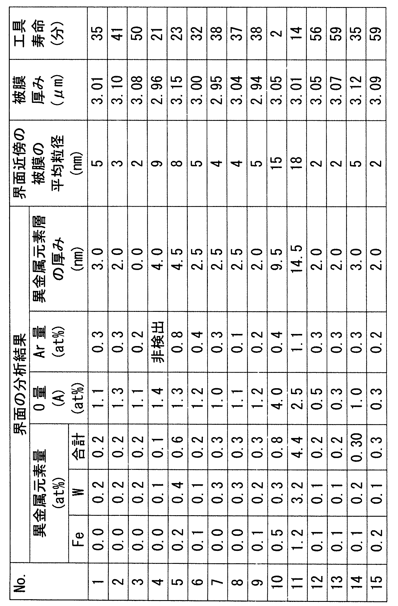
試料No.1~9,12~15の切削工具では、工具寿命が20分以上となり、被膜の耐剥離性に優れることが確認された。
試料No.1~9,12~15では、ボンバード処理において基材に印加されるバイアス電圧の絶対値が300V以下に制限されるため、チャンバ内の治具から放出されるFeの量が低減されるとともに、基材に接続された超硬合金から放出されるWの量が低減される。これにより、立方晶窒化硼素と被膜との界面において、Fe含有量が1at%以下であり、W含有量が1at%以下であることが確認された。
図2は、試料No.2における立方晶窒化硼素と被膜との界面を示す200万倍のTEM像(明視野像(bright-field image))である。図3は、試料No.2における立方晶窒化硼素と被膜との界面を示す200万倍のTEM像(HAADF像(high-angle annular dark field image))である。図2および図3に示されるように、界面にFe、Wおよび酸化物の層がほとんど見られず、被膜における界面近傍の結晶粒が小さいことがわかる。これは、立方晶窒化硼素の表面に存在するFe、W、O、Arが少ないことにより、成膜工程の際に、核発生と粒成長とが均一に起こるためである。すなわち、核発生がある場所に集中することが抑制されるとともに、粒成長しやすい場所と成長しにくい場所とが混在することも抑制される。
界面におけるFe含有量が1at%以下であり、W含有量が1at%以下であることにより、FeおよびWが被膜の結晶中に入り込むことによる被膜中の結晶の格子定数の増大化を抑制できる。その結果、基材中の立方晶窒化硼素の結晶と被膜の結晶との格子定数差の増大を抑制でき、立方晶窒化硼素と被膜との密着性が向上する。
さらに、試料No.1~9,12~15では、ボンバード開始前の水分圧が1×10⁻³Pa以下に制限されるとともに、ボンバード終了時の水分圧が5×10⁻³Pa以下に制限されている。これにより、立方晶窒化硼素と被膜との界面のO含有量が2at%以下に抑制され、Oに起因した立方晶窒化硼素と被膜との密着性の低下を抑制できる。
以上のように、界面におけるFe,WおよびOの含有量を低くすることにより、立方晶窒化硼素と被膜との密着性が向上し、試料No.1~9,12~15の切削工具における被膜の耐剥離性が向上したものと考えられる。
これに対し、試料No.10の切削工具では、工具寿命が2分と短いことが確認された。試料No.10では、ボンバード開始前の水分圧が1.98×10⁻³Paであり、ボンバード終了時の水分圧が7.93×10⁻³Paであるため、立方晶窒化硼素と被膜との界面におけるO含有量(at%)が2at%よりも高くなっている。その結果、立方晶窒化硼素と被膜との密着性が低下し、工具寿命が短くなったものと考えられる。
試料No.11の切削工具でも、工具寿命が14分と短いことが確認された。試料No.11では、ボンバード工程において基材に印加されるバイアス電圧が500Vと高いために、チャンバ内の治具から放出されるFe、および基材に接合された超硬合金から放出されるWの量が増大する。そのため、立方晶窒化硼素と被膜との界面におけるFeおよびWの合計含有量が4.4at%と多くなった。これにより、FeおよびWによって立方晶窒化硼素の結晶と被膜の結晶との格子定数差が広がり、立方晶窒化硼素と被膜との密着性が低下し、工具寿命が短くなったものと考えられる。
さらに、試料No.1~3,6~9,12~15では、工具寿命が30分以上となることが確認された。これは、異金属元素層の厚みが3nm以下であり、かつ界面近傍の被膜の平均粒径が5nm以下であることにより、立方晶窒化硼素と被膜との密着性がさらに向上したためと考えられる。そのため、異金属元素層の厚みを3nm以下とし、かつ界面近傍の被膜の平均粒径を5nm以下とすることが好ましいことが確認された。
さらに、試料No.2,3,12,13,15では、工具寿命が40分以上となることが確認された。これは、界面近傍の被膜の平均粒径が3nm以下であることにより、立方晶窒化硼素と被膜との界面の応力が緩和しやすくなったためと考えられる。そのため、界面近傍の被膜の平均粒径を3nm以下とすることが好ましいことが確認された。
以上のように本発明の実施の形態および実施例について説明を行なったが、上述の各実施の形態および実施例の構成を適宜組み合わせたり、様々に変形することも当初から予定している。
今回開示された実施の形態および実施例はすべての点で例示であって、制限的なものではないと考えられるべきである。本発明の範囲は上記した実施の形態および実施例ではなく請求の範囲によって示され、請求の範囲と均等の意味、および範囲内でのすべての変更が含まれることが意図される。
10 表面被覆cBN焼結体、 11 基材、 12 被膜、 100 切削工具、 100a すくい面、 100b 逃げ面、 101 台金、 102 ろう付け層。
Claims (7)
- 立方晶窒化硼素焼結体である基材と、
前記基材に接して前記基材を被覆する被膜とを備え、
前記基材中の立方晶窒化硼素と前記被膜との界面において、Fe含有量は1at%以下であり、W含有量は1at%以下であり、かつO含有量は2at%以下である、表面被覆立方晶窒化硼素焼結体。 - 前記Fe含有量と前記W含有量との合計含有量が0.05at%以上である層の厚みは5nm以下である、請求項1に記載の表面被覆立方晶窒化硼素焼結体。
- 前記被膜は多結晶体であり、
前記被膜における前記界面から10nm以内の領域は、平均粒径が10nm以下の結晶粒からなる、請求項1または請求項2に記載の表面被覆立方晶窒化硼素焼結体。 - 前記界面におけるAr含有量は1at%以下である、請求項1から請求項3のいずれか1項に記載の表面被覆立方晶窒化硼素焼結体。
- 前記被膜の厚みは0.3μm以上10μm以下である、請求項1から請求項4のいずれか1項に記載の表面被覆立方晶窒化硼素焼結体。
- 前記被膜は、Al,Ti,CrおよびSiからなる群より選択される少なくとも1種の元素と、CおよびNからなる群より選択される少なくとも1種の元素とからなる少なくとも1種の化合物を含む、請求項1から請求項5のいずれか1項に記載の表面被覆立方晶窒化硼素焼結体。
- 請求項1から請求項6のいずれか1項に記載の表面被覆立方晶窒化硼素焼結体を備えた切削工具。
Priority Applications (1)
| Application Number | Priority Date | Filing Date | Title |
|---|---|---|---|
| JP2019521955A JP7016866B2 (ja) | 2017-05-29 | 2018-02-21 | 表面被覆立方晶窒化硼素焼結体およびこれを備える切削工具 |
Applications Claiming Priority (2)
| Application Number | Priority Date | Filing Date | Title |
|---|---|---|---|
| JP2017-105583 | 2017-05-29 | ||
| JP2017105583 | 2017-05-29 |
Publications (1)
| Publication Number | Publication Date |
|---|---|
| WO2018220910A1 true WO2018220910A1 (ja) | 2018-12-06 |
Family
ID=64454509
Family Applications (1)
| Application Number | Title | Priority Date | Filing Date |
|---|---|---|---|
| PCT/JP2018/006170 Ceased WO2018220910A1 (ja) | 2017-05-29 | 2018-02-21 | 表面被覆立方晶窒化硼素焼結体およびこれを備える切削工具 |
Country Status (2)
| Country | Link |
|---|---|
| JP (1) | JP7016866B2 (ja) |
| WO (1) | WO2018220910A1 (ja) |
Cited By (1)
| Publication number | Priority date | Publication date | Assignee | Title |
|---|---|---|---|---|
| JP2021053740A (ja) * | 2019-09-30 | 2021-04-08 | 株式会社タンガロイ | 被覆工具 |
Citations (2)
| Publication number | Priority date | Publication date | Assignee | Title |
|---|---|---|---|---|
| JP2010029980A (ja) * | 2008-07-29 | 2010-02-12 | Kyocera Corp | 切削工具 |
| JP2015209354A (ja) * | 2014-04-25 | 2015-11-24 | 住友電工ハードメタル株式会社 | 複合焼結体および表面被覆窒化硼素焼結体工具 |
Family Cites Families (3)
| Publication number | Priority date | Publication date | Assignee | Title |
|---|---|---|---|---|
| US8178220B2 (en) * | 2004-04-30 | 2012-05-15 | Sumitomo Electric Hardmetal Corp. | Surface-covered cubic boron nitride sintered body tool and method of manufacturing the same |
| EP2778146B1 (en) * | 2011-11-07 | 2018-05-09 | Tungaloy Corporation | Cubic boron nitride sintered body |
| JP2015209534A (ja) * | 2014-04-30 | 2015-11-24 | 株式会社日本触媒 | (ポリ)アルキレングリコール化合物及び(ポリ)アルキレングリコール系重合体 |
-
2018
- 2018-02-21 WO PCT/JP2018/006170 patent/WO2018220910A1/ja not_active Ceased
- 2018-02-21 JP JP2019521955A patent/JP7016866B2/ja active Active
Patent Citations (2)
| Publication number | Priority date | Publication date | Assignee | Title |
|---|---|---|---|---|
| JP2010029980A (ja) * | 2008-07-29 | 2010-02-12 | Kyocera Corp | 切削工具 |
| JP2015209354A (ja) * | 2014-04-25 | 2015-11-24 | 住友電工ハードメタル株式会社 | 複合焼結体および表面被覆窒化硼素焼結体工具 |
Cited By (2)
| Publication number | Priority date | Publication date | Assignee | Title |
|---|---|---|---|---|
| JP2021053740A (ja) * | 2019-09-30 | 2021-04-08 | 株式会社タンガロイ | 被覆工具 |
| JP7467860B2 (ja) | 2019-09-30 | 2024-04-16 | 株式会社タンガロイ | 被覆工具 |
Also Published As
| Publication number | Publication date |
|---|---|
| JPWO2018220910A1 (ja) | 2020-03-26 |
| JP7016866B2 (ja) | 2022-02-07 |
Similar Documents
| Publication | Publication Date | Title |
|---|---|---|
| KR102268364B1 (ko) | 표면 피복 절삭 공구 및 그 제조 방법 | |
| JP6773287B2 (ja) | 表面被覆工具およびその製造方法 | |
| JP5297388B2 (ja) | 表面被覆切削工具 | |
| JP5098726B2 (ja) | 被覆工具及び被覆工具の製造方法 | |
| KR102198744B1 (ko) | 표면 피복 절삭 공구 | |
| JP5321975B2 (ja) | 表面被覆切削工具 | |
| EP3808477B1 (en) | Surface-coated cutting tool and process for producing same | |
| KR20190142359A (ko) | 피복 절삭 공구 | |
| JPWO2019171648A1 (ja) | 表面被覆切削工具及びその製造方法 | |
| JP6984108B2 (ja) | 表面被覆切削工具及びその製造方法 | |
| JP7016866B2 (ja) | 表面被覆立方晶窒化硼素焼結体およびこれを備える切削工具 | |
| JPWO2020075356A1 (ja) | 切削工具及びその製造方法 | |
| JP7055961B2 (ja) | 表面被覆切削工具及びその製造方法 | |
| JP7064438B2 (ja) | 切削工具およびその製造方法 | |
| JP6122975B2 (ja) | TixSi1−xN層を含んでなるコーティングによりワークピースをコーティングする方法 | |
| JP2012076156A (ja) | 超硬合金およびその製造方法 | |
| JP4697389B2 (ja) | 高速切削加工で硬質被覆層がすぐれた耐摩耗性を発揮する表面被覆超硬合金製切削工具 | |
| JP5327534B2 (ja) | 硬質被覆層の耐欠損性、耐剥離性に優れる表面被覆切削工具 | |
| JP2017166011A (ja) | 被膜、切削工具および被膜の製造方法 | |
| JP7286812B2 (ja) | 切削工具 | |
| JP2006015451A (ja) | 高速切削加工で硬質被覆層がすぐれた耐摩耗性を発揮する表面被覆超硬合金製切削工具の製造方法 | |
| JP2020152983A (ja) | 被覆切削工具及びその製造方法 | |
| JPH08174341A (ja) | 硬質膜被覆ツイストドリルおよびその製造方法 | |
| JP2005342856A (ja) | 断続重切削条件で硬質被覆層がすぐれた耐チッピング性を発揮する表面被覆超硬合金製切削工具 |
Legal Events
| Date | Code | Title | Description |
|---|---|---|---|
| 121 | Ep: the epo has been informed by wipo that ep was designated in this application |
Ref document number: 18810802 Country of ref document: EP Kind code of ref document: A1 |
|
| ENP | Entry into the national phase |
Ref document number: 2019521955 Country of ref document: JP Kind code of ref document: A |
|
| NENP | Non-entry into the national phase |
Ref country code: DE |
|
| 122 | Ep: pct application non-entry in european phase |
Ref document number: 18810802 Country of ref document: EP Kind code of ref document: A1 |