WO2018199258A1 - 電極、構造体およびその製造方法、接続構造体、並びに、その電極を用いた素子 - Google Patents
電極、構造体およびその製造方法、接続構造体、並びに、その電極を用いた素子 Download PDFInfo
- Publication number
- WO2018199258A1 WO2018199258A1 PCT/JP2018/017058 JP2018017058W WO2018199258A1 WO 2018199258 A1 WO2018199258 A1 WO 2018199258A1 JP 2018017058 W JP2018017058 W JP 2018017058W WO 2018199258 A1 WO2018199258 A1 WO 2018199258A1
- Authority
- WO
- WIPO (PCT)
- Prior art keywords
- alloy
- electrode
- layer
- atoms
- content
- Prior art date
- Legal status (The legal status is an assumption and is not a legal conclusion. Google has not performed a legal analysis and makes no representation as to the accuracy of the status listed.)
- Ceased
Links
- FXKMXDQBHDTQII-UHFFFAOYSA-N c(cc1)ccc1-[n](c(cccc1)c1c1c2)c1ccc2-c(cc1)cc(c2cc(-c(cc3)cc(c4ccccc44)c3[n]4-c3ccccc3)ccc22)c1[n]2-c1ccccc1 Chemical compound c(cc1)ccc1-[n](c(cccc1)c1c1c2)c1ccc2-c(cc1)cc(c2cc(-c(cc3)cc(c4ccccc44)c3[n]4-c3ccccc3)ccc22)c1[n]2-c1ccccc1 FXKMXDQBHDTQII-UHFFFAOYSA-N 0.000 description 1
Images





Classifications
-
- C—CHEMISTRY; METALLURGY
- C22—METALLURGY; FERROUS OR NON-FERROUS ALLOYS; TREATMENT OF ALLOYS OR NON-FERROUS METALS
- C22C—ALLOYS
- C22C23/00—Alloys based on magnesium
-
- H—ELECTRICITY
- H05—ELECTRIC TECHNIQUES NOT OTHERWISE PROVIDED FOR
- H05B—ELECTRIC HEATING; ELECTRIC LIGHT SOURCES NOT OTHERWISE PROVIDED FOR; CIRCUIT ARRANGEMENTS FOR ELECTRIC LIGHT SOURCES, IN GENERAL
- H05B33/00—Electroluminescent light sources
- H05B33/10—Apparatus or processes specially adapted to the manufacture of electroluminescent light sources
-
- H—ELECTRICITY
- H05—ELECTRIC TECHNIQUES NOT OTHERWISE PROVIDED FOR
- H05B—ELECTRIC HEATING; ELECTRIC LIGHT SOURCES NOT OTHERWISE PROVIDED FOR; CIRCUIT ARRANGEMENTS FOR ELECTRIC LIGHT SOURCES, IN GENERAL
- H05B33/00—Electroluminescent light sources
- H05B33/12—Light sources with substantially two-dimensional [2D] radiating surfaces
- H05B33/26—Light sources with substantially two-dimensional [2D] radiating surfaces characterised by the composition or arrangement of the conductive material used as an electrode
-
- H—ELECTRICITY
- H10—SEMICONDUCTOR DEVICES; ELECTRIC SOLID-STATE DEVICES NOT OTHERWISE PROVIDED FOR
- H10D—INORGANIC ELECTRIC SEMICONDUCTOR DEVICES
- H10D30/00—Field-effect transistors [FET]
- H10D30/60—Insulated-gate field-effect transistors [IGFET]
- H10D30/67—Thin-film transistors [TFT]
-
- H—ELECTRICITY
- H10—SEMICONDUCTOR DEVICES; ELECTRIC SOLID-STATE DEVICES NOT OTHERWISE PROVIDED FOR
- H10D—INORGANIC ELECTRIC SEMICONDUCTOR DEVICES
- H10D64/00—Electrodes of devices having potential barriers
- H10D64/01—Manufacture or treatment
- H10D64/011—Manufacture or treatment of electrodes ohmically coupled to a semiconductor
-
- H—ELECTRICITY
- H10—SEMICONDUCTOR DEVICES; ELECTRIC SOLID-STATE DEVICES NOT OTHERWISE PROVIDED FOR
- H10D—INORGANIC ELECTRIC SEMICONDUCTOR DEVICES
- H10D64/00—Electrodes of devices having potential barriers
- H10D64/20—Electrodes characterised by their shapes, relative sizes or dispositions
- H10D64/23—Electrodes carrying the current to be rectified, amplified, oscillated or switched, e.g. sources, drains, anodes or cathodes
-
- H—ELECTRICITY
- H10—SEMICONDUCTOR DEVICES; ELECTRIC SOLID-STATE DEVICES NOT OTHERWISE PROVIDED FOR
- H10K—ORGANIC ELECTRIC SOLID-STATE DEVICES
- H10K10/00—Organic devices specially adapted for rectifying, amplifying, oscillating or switching; Organic capacitors or resistors having potential barriers
- H10K10/40—Organic transistors
- H10K10/46—Field-effect transistors, e.g. organic thin-film transistors [OTFT]
-
- H—ELECTRICITY
- H10—SEMICONDUCTOR DEVICES; ELECTRIC SOLID-STATE DEVICES NOT OTHERWISE PROVIDED FOR
- H10K—ORGANIC ELECTRIC SOLID-STATE DEVICES
- H10K50/00—Organic light-emitting devices
- H10K50/10—OLEDs or polymer light-emitting diodes [PLED]
-
- Y—GENERAL TAGGING OF NEW TECHNOLOGICAL DEVELOPMENTS; GENERAL TAGGING OF CROSS-SECTIONAL TECHNOLOGIES SPANNING OVER SEVERAL SECTIONS OF THE IPC; TECHNICAL SUBJECTS COVERED BY FORMER USPC CROSS-REFERENCE ART COLLECTIONS [XRACs] AND DIGESTS
- Y02—TECHNOLOGIES OR APPLICATIONS FOR MITIGATION OR ADAPTATION AGAINST CLIMATE CHANGE
- Y02E—REDUCTION OF GREENHOUSE GAS [GHG] EMISSIONS, RELATED TO ENERGY GENERATION, TRANSMISSION OR DISTRIBUTION
- Y02E10/00—Energy generation through renewable energy sources
- Y02E10/50—Photovoltaic [PV] energy
- Y02E10/549—Organic PV cells
Definitions
- the present invention relates to an electrode, a structure, and a connection structure that can efficiently inject electrons into a semiconductor.
- the present invention also relates to an element using the electrode.
- a semiconductor element such as a transistor or an organic light-emitting element has a structure in which a metal electrode is connected to a semiconductor layer, and is configured to operate through charge transfer between the metal electrode and the semiconductor layer.
- a field-effect transistor includes a source electrode and a drain electrode provided separately, a semiconductor layer provided in contact with each electrode between the source electrode and the drain electrode, and a semiconductor layer that overlaps the semiconductor layer. And a gate electrode provided through a gate insulating layer.
- a charge flow channel channel is formed in the semiconductor layer, and the source electrode and the drain electrode are connected to each other. Current flows.
- the transistor functions as a switching element or a current amplifying element that controls on / off of the element connected to the drain electrode, for example.
- the electrode material of such a semiconductor element gold has been most frequently used so far (see, for example, Patent Documents 1 to 3). This is because gold is chemically stable, can be easily formed using vacuum deposition, and can be finely processed by a lift-off method using a photoresist.
- JP 2016-190826 A Japanese Patent Laid-Open No. 2015-170760 JP 2014-078730 A
- the present inventors provide an electrode, a structure, and a connection structure that have a low work function, can be brought into ohmic contact with a semiconductor layer, and have high lithography suitability.
- intensive investigations have been made for the purpose of providing an element having a low driving voltage and good characteristics by using such an electrode.
- the inventors have made an exhaustive study of forming electrodes with various metals and alloys, connecting them to a semiconductor layer, and evaluating their voltage-current characteristics.
- an electrode having an alloy containing Mg and Ca and a semiconductor layer are connected, an ideal result is obtained that the voltage-current curve increases linearly through the origin, and ohmic contact is realized. It came to obtain the knowledge that.
- MgCa electrode the knowledge that the weather resistance of an electrode improved by prescribing
- the present inventors have been proposed based on these findings, and specifically have the following configurations.
- General formula (1) MgCa (X) n [In General Formula (1), n represents 0 or 1. When n is 0, the content of Ca contained in the alloy is 5 to 30 atomic% of the total number of atoms in the alloy. When n is 1, X represents one or more atoms selected from Ag, Al, Cr, Cu, Zn and Li, and the content of Mg contained in the alloy is 50 to 95 atoms of the total number of atoms in the alloy The Ca content in the alloy is 1 to 50 atomic% of the total number of atoms of the alloy, and the Ag content in the alloy is 0.1 to 30 atomic% of the total number of atoms of the alloy. is there.
- [7] A structure having irregularities having a pitch of 500 nm to 200 ⁇ m on the surface, made of an alloy represented by the general formula (1).
- [8] The structure according to [7], wherein the plurality of strips made of the alloy have a structure in which the strips are arranged in parallel at a pitch of 500 nm to 200 ⁇ m.
- a method for manufacturing a structure including a step of forming the alloy represented by the general formula (1) by a lithography method.
- the method for manufacturing a structure according to any one of [9] to [12], wherein the alloy is an alloy film formed on a substrate.
- connection structure having a structure in which an alloy represented by the general formula (1) and a semiconductor are electrically connected.
- the electrode of the present invention Since the electrode of the present invention has a small work function, when connected to the semiconductor layer, the energy barrier against electron injection from the electrode to the semiconductor layer is low, and electrons can be efficiently injected into the semiconductor layer.
- the contact state with the semiconductor layer can be ohmic contact.
- the electrode of the present invention has high lithography suitability, and can be finely processed precisely using a lithography method.
- the electrode of the present invention has excellent weather resistance and exhibits barrier properties against oxygen and water vapor. Since the element of the present invention uses such an electrode, the driving voltage is low, good characteristics are obtained, and the durability is high.
- a numerical range represented by using “to” means a range including numerical values described before and after “to” as a lower limit value and an upper limit value.
- the isotope species of the hydrogen atom present in the molecule of the compound used in the present invention is not particularly limited. For example, all the hydrogen atoms in the molecule may be 1 H, or a part or all of the hydrogen atoms are 2 H. (Deuterium D) may be used. Further, the contents (atomic%) of materials other than the atoms represented by Mg, Ca, and X and the alloy represented by the general formula (1) in this specification are measured by an energy dispersive X-ray analyzer. It is what is done.
- Electrode The electrode of this invention has the alloy represented by following General formula (1), It is characterized by the above-mentioned.
- General formula (1) MgCa (X) n
- n represents 0 or 1.
- the content of Ca contained in the alloy is 5 to 30 atomic% of the total number of atoms in the alloy.
- X represents one or more atoms selected from Ag, Al, Cr, Cu, Zn and Li
- the content of Mg contained in the alloy is 50 to 95 atoms of the total number of atoms in the alloy
- the Ca content in the alloy is 1 to 50 atomic% of the total number of atoms of the alloy
- the Ag content in the alloy is 0.1 to 30 atomic% of the total number of atoms of the alloy. is there.
- the alloy represented by the general formula (1) means an alloy containing only Mg and Ca as alloy components.
- an alloy represented by the general formula (1) when n is 0 is referred to as an MgCa alloy.
- the Ca content in the MgCa alloy is 5 to 30 atomic% of the total number of atoms in the alloy, and the remainder is the Mg content.
- the alloy represented by the general formula (1) means an alloy having Mg and Ca and atoms represented by X as alloy components.
- an alloy represented by the general formula (1) when n is 1 is referred to as an MgCaX alloy.
- X is one or more atoms selected from Ag, Al, Cr, Cu, Zn and Li, and may be one kind of atom or two or more kinds of atoms.
- the content of each atom in the MgCaX alloy is not particularly limited, and the three or more types of atoms may be included in the alloy, and the total amount may be 100 atomic%.
- “Inevitable impurity element” means an element having a content of 1 atomic% or less in the alloy, and the content is preferably 0.1 atomic% or less, and 0.01 atomic% or less. Is more preferable, and it is further more preferable that it is 0.001 atomic% or less.
- the alloy represented by the general formula (1) used in the present invention has a low work function of 4 eV or less.
- the electrode having the alloy represented by the general formula (1) has a low energy barrier against electron injection from the electrode to the semiconductor layer in the connection structure between the electrode and the semiconductor layer, and efficiently injects electrons into the semiconductor layer.
- the contact state with the semiconductor layer can be ohmic contact. Thereby, the drive voltage of the element using this electrode can be lowered and good element characteristics can be realized.
- the alloy represented by the general formula (1) can be easily formed using a vapor phase process, and the alloy film can be finely processed precisely using a lithography method. Suitable for microfabrication.
- Mg and Ca which are constituent elements of this alloy film, are not rare elements such as Au, and thus are inexpensive.
- the manufacturing cost of an element can be reduced by comprising an electrode with the alloy represented by General formula (1).
- the alloy represented by the general formula (1) has excellent barrier properties against oxygen and water vapor, and the weather resistance of the device can be improved by using this alloy for an electrode. Thereby, instead of an expensive gas barrier film having a high barrier property, an inexpensive gas barrier film having a relatively low barrier property can be used, so that the manufacturing cost of the element can be further reduced.
- the alloy represented by the general formula (1) has a high reflectance with respect to light in the visible region.
- the alloy represented by the general formula (1) used in the present invention is an MgCa alloy containing only Mg and Ca as an alloy component when n is 0, and Ca contained in the MgCa alloy.
- the content is 5 to 30 atomic% of the total number of atoms of the alloy, and the balance is the Mg content.
- an MgCa alloy having a Ca content of 5 to 30 atomic% is excellent in weather resistance and exhibits a barrier property against oxygen and water vapor.
- performance deterioration with time or electrode It was also found that shape deformation can be suppressed.
- the Ca content of the MgCa alloy in the present invention is defined based on these findings.
- the MgCa alloy used in the present invention has a Ca content of 5 to 30 atomic%, and thus has a low work function, and realizes a low energy barrier and ohmic contact in the connection structure between the electrode and the semiconductor layer. Can do.
- the element is provided with a barrier property against oxygen and water vapor, and deterioration of performance over time and deformation of the electrode during element storage can be suppressed.
- the device is provided with a barrier property against oxygen or water vapor, an expensive gas barrier exhibiting a high barrier property of 10 ⁇ 6 gm ⁇ 2 day ⁇ 1 level even in an organic electroluminescence device that is weak against oxygen or water.
- the preferable range of the Ca content of the MgCa alloy is 5 to 18 atomic%.
- the reflectance of the MgCa alloy is increased. For example, when an electrode having the MgCa alloy is disposed on the side opposite to the light extraction side of the light emitting element, the light emitted from the light emitting layer is efficiently reflected by the electrode. It can be taken out on the take-out side. As a result, high luminous efficiency can be obtained.
- the lower limit of the Ca content of the MgCa alloy is preferably more than 6 atomic%, more preferably 9 atomic% or more, and the upper limit is more preferably less than 16 atomic%, More preferably, it is at most atomic%.
- the Ca content of the MgCa alloy is within the range defined by the above lower limit, performance deterioration during device storage can be more effectively suppressed.
- the Ca content of the MgCa alloy is within the range defined by the above upper limit, the work function can be made lower.
- the alloy represented by the general formula (1) used in the present invention is an MgCaX alloy having an atom represented by Mg, Ca and X as an alloy component when n is 1.
- the content of each atom contained in the MgCaX alloy is not particularly limited, but the Mg content is preferably 50 to 95 atomic% of the total number of atoms of the alloy, more preferably 70 to 95 atoms of the total number of atoms of the alloy. %.
- the atom represented by X of the MgCaX alloy is one or more atoms selected from Ag, Al, Cr, Cu, Zn and Li, and may be one kind of atom or a combination of two or more kinds of atoms. Good.
- the MgCaX alloy contains atoms represented by X in addition to Mg and Ca, thereby controlling the work function of the electrode and improving conductivity and barrier properties.
- the atom represented by X is preferably one or more atoms selected from Ag and Al.
- Preferred examples of the MgCaX alloy in which one or more atoms selected from Ag and Al are X include MgCaAg alloy, MgCaAl alloy, and MgCaAgAl alloy.
- the content of atoms represented by X is preferably 0.1 to 30 atomic percent, more preferably 1 to 30 atomic percent of the total number of atoms in the alloy.
- the lower limit may be selected from the range of 1 atom% or more, 3 atom% or more, 5 atom% or more, and the upper limit is 23 atom% or less, 16 atom% or less, 10 atom% or less, 6 atom% or less. You may select from the range.
- the Ca content is preferably 1 to 50 atomic%, more preferably 3 to 50 atomic% of the total number of atoms in the alloy.
- the lower limit may be selected from the range of 2 atomic% or more, 3 atomic% or more, 5 atomic% or more, and the upper limit is 30 atomic% or less, 20 atomic% or less, 10 atomic% or less, 6 atomic% or less. You may select from the range.
- the total content of atoms represented by Ca and X is preferably 5 to 50 atomic%, more preferably 10 to 30 atomic% of the total number of atoms in the alloy.
- the content of atoms represented by X is preferably 0.2 to 5.0 times the number of Ca atoms.
- the lower limit is 0.3 times or more and 0.6 times or more of the number of Ca atoms.
- the total content thereof corresponds to the content of the atoms represented by X described above.
- the total content of Ca and Mg in the MgCaX alloy is, for example, 70 atomic% or more, 77 atomic% or more, 84 atomic% or more, 90 atomic% or more, 95 atomic% or more, 99 atomic% or more of the total number of atoms of the alloy, You may select from the range of 99.9 atomic% or more.
- the content of Mg contained in the alloy is 50 to 95 atomic% of the total number of atoms of the alloy, and the content of Ca contained in the alloy is 1 to 50 atomic% of the total number of atoms of the alloy.
- a composition in which the X content in the alloy is 0.1 to 30 atomic% of the total number of atoms in the alloy, or a Mg content in the alloy is in the range of 50 to 95 atoms in the total number of atoms of the alloy.
- the Ca content in the alloy is 3 to 50 atomic% of the total number of atoms of the alloy, and the X content in the alloy is 0.1 to 30 atomic% of the total number of atoms of the alloy.
- a certain composition etc. can be selected preferably.
- the electrode of the present invention and the layer having the alloy represented by the general formula (1) constituting the laminated structure described later may be composed of only the alloy represented by the general formula (1). Materials other than alloys may be included.
- the electrode and the layer include a material other than the alloy represented by the general formula (1), the content of the material other than the alloy is, for example, 20% by weight or less, 10% by weight or less, 5% by weight or less, 1 It may be selected within a range of not more than wt% and not more than 0.1 wt%.
- the material other than the alloy may be an inorganic material or an organic material, or may be a composite material of an inorganic material and an organic material.
- the aspect of materials other than an alloy is not specifically limited, For example, it may be disperse
- the shape of the electrode of the present invention is not particularly limited, and a known electrode shape such as a layer shape, a column shape, a bump shape, or a wire shape can be employed.
- a semiconductor element such as a transistor, an organic light emitting element, or a solar cell
- a layered electrode is provided.
- the electrode of the present invention When the electrode of the present invention is layered, it may have a single-layer configuration of a layer having an alloy represented by the general formula (1), or two layers having an alloy represented by the general formula (1).
- a multilayer structure in which the layers are laminated as described above may be used, or a multilayer structure in which a layer having an alloy represented by the general formula (1) and another layer are laminated may be employed.
- the other layer is a layer that does not have the alloy represented by the general formula (1), and may be a layer made of an inorganic material or a layer made of an organic material. It may be a layer made of a composite material.
- the other layer may contain one of Mg and Ca.
- the number of layers having the alloy represented by the general formula (1) and the number of other layers is one each. Or multiple layers.
- the constituent components of each layer and the content ratios and thicknesses of the constituent components may be the same or different, but adjacent layers are at least a part of the constituent components. It is preferable that at least one of the content ratios of the constituent components is different.
- the thickness and planar shape of the electrode are not particularly limited, and can be appropriately selected according to the usage mode.
- the “planar shape of the electrode” in the present specification means a shape in a plan view when the electrode is viewed from a direction orthogonal to the thickness direction.
- the thickness is preferably 10 to 2000 nm, and more preferably 10 to 1000 nm. More preferably, it is 10 to 100 nm.
- the planar shape of the electrode may be a continuous shape as a whole or a shape composed of a plurality of separated parts.
- the shape of each part of the whole continuous shape and the shape consisting of a plurality of parts is not particularly limited, and is a strip, a line, a lattice, a square, a rectangle, a circle, an ellipse, an oval, Any of semicircular shape, indefinite shape, etc. may be sufficient.
- the electrode may form a repeating pattern in which two or more parts having the same shape are arranged in parallel with a space therebetween. Examples of the repetitive pattern include a stripe shape, a lattice shape, and a dot shape.
- the pitch between adjacent portions in the repetitive pattern is preferably 500 nm to 200 ⁇ m, more preferably 500 nm to 100 ⁇ m, and even more preferably 500 nm to 50 ⁇ m.
- the pitch refers to the distance between the center of one part and the center of the adjacent part.
- the planar shape of the electrode is a stripe
- the distance between the center of the electrode line in the minor axis direction and the center of the electrode line adjacent thereto in the minor axis direction corresponds to the pitch.
- the width (short axis length) of the electrode line is preferably 500 nm to 2000 ⁇ m, more preferably 500 nm to 1000 ⁇ m, and more preferably 500 nm to 500 ⁇ m. Further preferred.
- the “work function” refers to a photoelectric work function measured using a photoelectron spectrometer.
- the work function of the electrode is preferably 4.5 eV or less, more preferably 2.5 to 4.5 eV, and even more preferably 2.5 to 4.0 eV.
- the work function of the electrode is preferably selected in accordance with the energy state of the connected body that is electrically connected to the electrode. For example, when the body to be connected is an organic semiconductor, the work function of the electrode is E LUMO ⁇ 1.5 eV, where the absolute value of the LUMO (Lowest Unoccupied Molecular Orbital) level of the organic semiconductor is E LUMO.
- the work function of the electrode is ⁇ ⁇ 1.5 eV, where ⁇ is the electron affinity of the inorganic semiconductor, that is, the energy from the bottom of the conduction band to the vacuum level.
- ⁇ is the electron affinity of the inorganic semiconductor, that is, the energy from the bottom of the conduction band to the vacuum level.
- ⁇ is the electron affinity of the inorganic semiconductor, that is, the energy from the bottom of the conduction band to the vacuum level.
- it is ⁇ ⁇ 1.0 eV, more preferably ⁇ ⁇ 0.5 eV.
- the work function of the electrode is particularly preferably less than or equal to the work function of the connected body.
- the LUMO level of the organic semiconductor can be measured by an optical energy gap calculated from the absorption edge of the absorption spectrum or by inverse photoelectron spectroscopy.
- the electron affinity of the inorganic semiconductor can be measured by an optical energy gap calculated from the absorption edge of the absorption spectrum or inverse photoelectron spectroscopy.
- the “reflectance with respect to light in the visible region” refers to a value measured by a spectroscopic ellipsometry apparatus or a spectral transmittance / reflectance measuring apparatus.
- the reflectance of the electrode with respect to light in the visible region (380 to 780 nm) is preferably 80% or more, more preferably 85% or more, and further preferably 90% or more.
- the reflectance of the electrode is preferably in the above-mentioned range over the entire visible region, but the reflectance may be in the above-mentioned range may be a part of the visible region.
- the reflectance of the light emitting wavelength region of the organic light emitting device is preferably in the above range.
- the structure of the present invention is made of an alloy represented by the general formula (1), and has irregularities having a pitch of 500 nm to 200 ⁇ m on the surface.
- the structure of the present invention may have a single layer configuration of a layer made of an alloy represented by the general formula (1) or a multilayer configuration of a layer made of an alloy represented by the general formula (1). Also good.
- the presence / absence of atoms represented by X in each layer, the type and the content ratio of components, and the thickness may be the same or different, but adjacent layers are represented by X. It is preferable that at least one of the presence / absence of atoms, the type, and the content ratio of the constituent components is different.
- corrugation in this invention contains the shape which convex parts isolate
- the concave and convex portions of the structure have a repeating pattern in which two or more convex portions having the same shape are arranged in parallel with each other in a plan view viewed from the top side of the convex portion.
- the repetitive pattern include a stripe shape, a lattice shape, and a dot shape in which a plurality of strips are arranged in parallel.
- the “pitch” in the present invention refers to the distance between the center of the convex portion in plan view and the center of the convex portion adjacent thereto, for example, when the convex portion is in a stripe shape or a lattice shape. The distance between the center of the convex part in the short axis direction and the center of the convex part adjacent to the convex part in the short axis direction corresponds to the pitch.
- the manufacturing method of the structure of this invention includes the process of forming an unevenness
- Specific examples can be referred to the explanation, preferred range and specific examples of the alloy represented by the general formula (1) of the electrode. it can.
- the description of the unevenness and the specific examples of the preferable range and shape the description of the unevenness and the preferable range and specific shape in the section of the structure can be referred to.
- the “lithography method” in the present invention means that an alloy represented by the general formula (1) is formed in a predetermined pattern.
- the alloy represented by the general formula (1) may be directly formed so as to have a predetermined pattern, or after the alloy film is uniformly formed, a part of the alloy film is removed to obtain a predetermined pattern. Although it may be formed into a pattern, the latter method is preferred. In the latter method, part of the alloy film can be removed by, for example, locally etching an unnecessary part of the alloy film, and it is preferable to use a mask having a predetermined pattern.
- a mask having a predetermined pattern is formed by irradiating and developing a part of a film made of an energy ray-sensitive material that is cured or solubilized by the action of energy rays, and developing the mask.
- the pattern or the reverse pattern is transferred to the alloy film.
- the lithography method using a mask include a photolithography method, an X-ray lithography method, an electron beam lithography method, an extreme ultraviolet lithography method, an ion beam lithography method, and the like, and it is preferable to use a photolithography method.
- the energy beam sensitive material used in the lithography method a negative resin composition that is cured by the action of energy rays, a positive resist film that is solubilized by the action of energy rays, or the like can be used.
- the manufacturing process of the structure by the lithography method is not particularly limited, for example, the following first manufacturing method or second manufacturing method can be used.
- a substrate for forming an alloy film is prepared, a film made of an energy beam sensitive material is formed on the substrate, and developed by irradiating the energy beam to develop a mask of a reverse pattern with respect to the target pattern. Form.
- an alloy represented by the general formula (1) is uniformly formed on the substrate so as to cover the mask, thereby obtaining an alloy film.
- the method for forming the alloy represented by the general formula (1) is not particularly limited. For example, a vapor deposition process such as vacuum deposition, sputtering, ion plating, plating such as electrolytic plating, immersion plating, electroless plating, thermal spraying, joining of metal foil, etc. can be used. It is preferable to form an alloy film.
- the mask and the alloy film immediately above the mask are removed by using a solvent.
- a solvent As a result, only the alloy film in the region where the mask is not formed remains on the substrate, and an alloy film formed into a mask reversal pattern (target pattern) is obtained.
- An alloy film is obtained by uniformly forming an alloy represented by the general formula (1) on the substrate.
- the method for forming the alloy film the method for forming the alloy film in the first manufacturing method can be referred to.
- a film made of an energy beam sensitive material is formed on the alloy film, and a mask having a target pattern is formed by developing by irradiating the energy beam.
- the mask on the alloy film is removed by peeling. As a result, only the alloy film in the region where the mask was formed remains on the substrate, and an alloy film formed into a mask pattern (target pattern) is obtained.
- etching method of the alloy film a dry etching method such as plasma etching, sputter etching, reactive ion etching, sputter ion beam etching, reactive ion beam etching, or a wet etching method can be used.
- the base material for forming the alloy film can be appropriately selected according to the element to which the structure of the present invention is applied.
- the element to which the structure of the present invention is applied is an organic light-emitting element, a transistor, or a solar cell
- the substrate illustrated below or a layer directly below the electrode may be used as a base material. it can.
- the first manufacturing method and the second manufacturing method it is preferable to use the first manufacturing method because unnecessary portions of the alloy film can be removed without etching and the process is simple. .
- connection structure of this invention has the electrode which has the alloy represented by General formula (1), and the semiconductor layer connected to this electrode.
- This connection structure can be used, for example, as a connection structure between an electrode and a semiconductor layer in a semiconductor element.
- the electrode having the alloy represented by the general formula (1) the preferred range, and a specific example, the description of the above-mentioned electrode can be referred to.
- the semiconductor layer connected to the electrode can be appropriately selected according to the element to which the connection structure of the present invention is applied.
- an electron transport layer in an organic light-emitting element described later a semiconductor layer in a transistor (preferably an n-channel semiconductor) Layer, n-type organic semiconductor layer), and a semiconductor layer corresponding to a photoelectric conversion layer or an electron extraction layer in a solar cell can be used.
- a semiconductor layer in a transistor preferably an n-channel semiconductor) Layer, n-type organic semiconductor layer
- a semiconductor layer corresponding to a photoelectric conversion layer or an electron extraction layer in a solar cell can be used.
- the work function of the electrode is small, the energy barrier against electron injection from the electrode to the semiconductor layer is low, electrons can be efficiently injected into the semiconductor layer, and the contact state between the electrode and the semiconductor layer Can be in ohmic contact.
- the connection structure which contributes to the reduction of the drive voltage of an element and the improvement of a voltage-current characteristic can be obtained.
- the ohmic contact between the electrode and the semiconductor layer means that a transistor in which the electrode is connected to the semiconductor layer as a source electrode and a drain electrode is produced, and the drain voltage-drain current curve passes through the origin and is a linear function. It can be confirmed with an increase.
- the element of the present invention has the electrode of the present invention. Since the electrode of the present invention has a low work function, when connected to a semiconductor layer, the energy barrier against electron injection from the electrode to the semiconductor layer is low, and electrons can be efficiently injected into the semiconductor layer. The contact state with the layer can be ohmic contact. For this reason, the element having the electrode of the present invention has a low driving voltage and can obtain good element characteristics.
- the element of the present invention is a semiconductor element having a connection structure in which an electrode and a semiconductor layer are electrically connected, and the electrode electrically connected to the semiconductor layer is preferably constituted by the electrode of the present invention. . Examples of the semiconductor element include an organic light emitting element, a transistor, and a solar cell. Hereinafter, an organic light emitting device, a transistor, and a solar cell will be described as the device of the present invention. However, the element of the present invention should not be limitedly interpreted by these specific examples.
- the organic light emitting device of the present invention is preferably an organic electroluminescent device that emits light from a light emitting material by current excitation.
- the organic electroluminescent element has at least an anode, a cathode, and a structure in which an organic layer is formed between the anode and the cathode, and the cathode is preferably composed of the electrode of the present invention.
- the organic layer includes at least a light emitting layer, and may consist of only the light emitting layer, or may have one or more organic layers in addition to the light emitting layer.
- Examples of such other organic layers include a hole transport layer, a hole injection layer, an electron blocking layer, a hole blocking layer, an electron injection layer, an electron transport layer, and an exciton blocking layer.
- the hole transport layer may be a hole injection / transport layer having a hole injection function
- the electron transport layer may be an electron injection / transport layer having an electron injection function.
- FIG. 1 A specific example of the structure of an organic electroluminescence element is shown in FIG. In FIG. 1, 1 is a substrate, 2 is an anode, 3 is a hole injection layer, 4 is a hole transport layer, 5 is a light emitting layer, 6 is an electron transport layer, and 7 is a cathode. Below, each member and each layer of an organic electroluminescent element are demonstrated.
- the organic electroluminescence device of the present invention is preferably supported on a substrate.
- the substrate is not particularly limited and may be any substrate conventionally used for organic electroluminescence elements.
- a substrate made of glass, transparent plastic, quartz, silicon, or the like can be used.
- an electrode material made of a metal, an alloy, an electrically conductive compound, or a mixture thereof having a high work function (4 eV or more) is preferably used.
- electrode materials include metals such as Au, and conductive transparent materials such as CuI, indium tin oxide (ITO), SnO 2 , and ZnO.
- conductive transparent materials such as CuI, indium tin oxide (ITO), SnO 2 , and ZnO.
- an amorphous material such as IDIXO (In 2 O 3 —ZnO) capable of forming a transparent conductive film may be used.
- a thin film may be formed by vapor deposition or sputtering of these electrode materials, and a pattern of a desired shape may be formed by photolithography, or when pattern accuracy is not so high (about 100 ⁇ m or more) ), A pattern may be formed through a mask having a desired shape at the time of vapor deposition or sputtering of the electrode material.
- wet film-forming methods such as a printing system and a coating system, can also be used.
- the transmittance be greater than 10%, and the sheet resistance as the anode is preferably several hundred ⁇ / ⁇ or less.
- the film thickness depends on the material, it is usually selected in the range of 10 to 1000 nm, preferably 10 to 200 nm.
- the cathode is constituted by the electrode of the present invention. Since the electrode of the present invention has a small work function, by constituting the cathode with the electrode of the present invention, electrons can be efficiently transferred to the organic layer (the electron transport layer 6 in the organic electroluminescence device shown in FIG. 1) bonded thereto. While being able to inject
- the work function of the electrode used for the cathode of the organic electroluminescence element is preferably E LUMO ⁇ 1.5 eV, where E LUMO is the absolute value of the LUMO level of the organic layer bonded to the cathode, E LUMO ⁇ 1.0 eV is more preferable, and E LUMO ⁇ 0.5 eV is even more preferable.
- the light emitting layer is a layer that emits light after excitons are generated by recombination of holes and electrons injected from each of the anode and the cathode, and the light emitting material may be used alone for the light emitting layer. , Preferably including a luminescent material and a host material. As the light emitting material, a fluorescent material, a phosphorescent material, a delayed fluorescent material, or the like can be used. In order for the organic electroluminescence device of the present invention to exhibit high luminous efficiency, it is important to confine singlet excitons and triplet excitons generated in the light emitting material in the light emitting material.
- a host material in addition to the light emitting material in the light emitting layer.
- the host material an organic compound in which at least one of excited singlet energy and excited triplet energy has a value higher than that of the light-emitting material can be used.
- singlet excitons and triplet excitons generated in the light emitting material can be confined in the molecule of the light emitting material, and the light emission efficiency can be sufficiently extracted.
- high luminous efficiency can be obtained, so that host materials that can achieve high luminous efficiency are particularly limited. And can be used in the present invention.
- light emission is generated from the light emitting material contained in the light emitting layer.
- This emission includes both fluorescence and delayed fluorescence.
- light emission from the host material may be partly or partly emitted.
- the amount of the light emitting material contained in the light emitting layer is preferably 0.1% by weight or more, more preferably 1% by weight or more, and 50% by weight or less. Is preferably 20% by weight or less, more preferably 10% by weight or less.
- the host material in the light-emitting layer is preferably an organic compound that has a hole transporting ability and an electron transporting ability, prevents the emission of longer wavelengths, and has a high glass transition temperature.
- the light emitting material can be selected in consideration of the wavelength to be emitted.
- a light emitting material such as a phosphorescent light emitting material, a fluorescent material such as a heat activated delayed fluorescent material, or an exciplex light emitting material can be appropriately selected and used.
- the light emitting material include a dye material, a metal complex material, a polymer material, and a dopant material.
- dye-based materials include cyclopentamine derivatives, tetraphenylbutadiene derivative compounds, triphenylamine derivatives, oxadiazole derivatives, pyrazoloquinoline derivatives, distyrylbenzene derivatives, distyrylarylene derivatives, pyrrole derivatives, thiophene ring compounds. Pyridine ring compounds, perinone derivatives, perylene derivatives, oligothiophene derivatives, oxadiazole dimers, pyrazoline dimers, quinacridone derivatives, coumarin derivatives, and the like.
- the metal complex material examples include rare earth metals such as Tb, Eu, and Dy, or Al, Zn, Be, Pt, Ir, and the like as a central metal, and oxadiazole, thiadiazole, phenylpyridine, phenylbenzimidazole, and quinoline.
- Examples include metal complexes having a structure as a ligand, for example, iridium complexes, platinum complexes and other metal complexes having light emission from a triplet excited state, aluminum quinolinol complexes, benzoquinolinol beryllium complexes, benzoxazolyl zinc A complex, a benzothiazole zinc complex, an azomethylzinc complex, a porphyrin zinc complex, a phenanthroline europium complex, and the like can be given.
- metal complexes having a structure as a ligand for example, iridium complexes, platinum complexes and other metal complexes having light emission from a triplet excited state, aluminum quinolinol complexes, benzoquinolinol beryllium complexes, benzoxazolyl zinc A complex, a benzothiazole zinc complex, an azomethylzinc complex, a porphyrin zinc complex, a phenanthroline europium complex, and the
- polystyrene resins polyparaphenylene vinylene derivatives, polythiophene derivatives, polyparaphenylene derivatives, polysilane derivatives, polyacetylene derivatives, polyfluorene derivatives, polyvinyl carbazole derivatives, the above dye materials and metal complex light emitting materials are polymerized. The thing etc. can be mentioned.
- examples of the material that emits blue light include distyrylarylene derivatives, oxadiazole derivatives, and polymers thereof, polyvinylcarbazole derivatives, polyparaphenylene derivatives, and polyfluorene derivatives.
- polymer materials such as polyvinyl carbazole derivatives, polyparaphenylene derivatives, and polyfluorene derivatives are preferred.
- examples of materials that emit green light include quinacridone derivatives, coumarin derivatives, and polymers thereof, polyparaphenylene vinylene derivatives, polyfluorene derivatives, and the like. Of these, polymer materials such as polyparaphenylene vinylene derivatives and polyfluorene derivatives are preferred.
- Examples of materials that emit red light include coumarin derivatives, thiophene ring compounds, and polymers thereof, polyparaphenylene vinylene derivatives, polythiophene derivatives, and polyfluorene derivatives.
- polymer materials such as polyparaphenylene vinylene derivatives, polythiophene derivatives, and polyfluorene derivatives are preferable.
- phosphorescent materials include Irr complexes such as Flrpic, FCNIr, Ir (dbfmi), FIr6, Ir (fbppz) 2 (dfbdp), FIrN4, and [Cu (dnbp) (DPEPhos)] BF 4 described later.
- [Cu (dppb) (DPEPhos)] BF4 [Cu ( ⁇ -l) dppb] 2, [Cu ( ⁇ -Cl) DPEphos] 2, Cu (2-tzq) (DPEPhos), [Cu (PNP))
- Compound 1001 Cu complexes such as Cu (Bpz4) (DPEPhos), and Pt complexes such as FPt and Pt-4 can be mentioned as preferred examples.
- thermally activated delayed fluorescent material for example, the following PIC-TRZ, [Cu (PNP-tBu)] 2 can be cited as a preferred example.
- Preferred examples of the exciplex light emitting material include the following m-MTDATA and PBD, PyPySPyPy and NPB, and PPSPP and NPB.
- the injection layer is a layer provided between the electrode and the organic layer for lowering the driving voltage and improving the luminance of light emission.
- the injection layer can be provided as necessary.
- the blocking layer is a layer that can prevent diffusion of charges (electrons or holes) and / or excitons existing in the light emitting layer to the outside of the light emitting layer.
- the electron blocking layer can be disposed between the light emitting layer and the hole transport layer and blocks electrons from passing through the light emitting layer toward the hole transport layer.
- a hole blocking layer can be disposed between the light emitting layer and the electron transporting layer to prevent holes from passing through the light emitting layer toward the electron transporting layer.
- the blocking layer can also be used to block excitons from diffusing outside the light emitting layer. That is, each of the electron blocking layer and the hole blocking layer can also function as an exciton blocking layer.
- the term “electron blocking layer” or “exciton blocking layer” as used herein is used in the sense of including a layer having the functions of an electron blocking layer and an exciton blocking layer in one layer.
- the hole blocking layer has a function of an electron transport layer in a broad sense.
- the hole blocking layer has a role of blocking holes from reaching the electron transport layer while transporting electrons, thereby improving the recombination probability of electrons and holes in the light emitting layer.
- the material for the hole blocking layer the material for the electron transport layer described later can be used as necessary.
- the electron blocking layer has a function of transporting holes in a broad sense.
- the electron blocking layer has a role to block electrons from reaching the hole transport layer while transporting holes, thereby improving the probability of recombination of electrons and holes in the light emitting layer. .
- the exciton blocking layer is a layer for preventing excitons generated by recombination of holes and electrons in the light emitting layer from diffusing into the charge transport layer. It becomes possible to efficiently confine in the light emitting layer, and the light emission efficiency of the device can be improved.
- the exciton blocking layer can be inserted on either the anode side or the cathode side adjacent to the light emitting layer, or both can be inserted simultaneously.
- the layer when the exciton blocking layer is provided on the anode side, the layer can be inserted adjacent to the light emitting layer between the hole transport layer and the light emitting layer, and when inserted on the cathode side, the light emitting layer and the cathode Between the luminescent layer and the light-emitting layer.
- a hole injection layer, an electron blocking layer, or the like can be provided between the anode and the exciton blocking layer adjacent to the anode side of the light emitting layer, and the excitation adjacent to the cathode and the cathode side of the light emitting layer can be provided.
- an electron injection layer, an electron transport layer, a hole blocking layer, and the like can be provided.
- the blocking layer is disposed, at least one of the excited singlet energy and the excited triplet energy of the material used as the blocking layer is preferably higher than the excited singlet energy and the excited triplet energy of the light emitting material.
- the hole transport layer is made of a hole transport material having a function of transporting holes, and the hole transport layer can be provided as a single layer or a plurality of layers.
- the hole transport material has any one of hole injection or transport and electron barrier properties, and may be either organic or inorganic.
- hole transport materials that can be used include, for example, triazole derivatives, oxadiazole derivatives, imidazole derivatives, carbazole derivatives, indolocarbazole derivatives, polyarylalkane derivatives, pyrazoline derivatives and pyrazolone derivatives, phenylenediamine derivatives, arylamine derivatives, Examples include amino-substituted chalcone derivatives, oxazole derivatives, styrylanthracene derivatives, fluorenone derivatives, hydrazone derivatives, stilbene derivatives, silazane derivatives, aniline copolymers, and conductive polymer oligomers, particularly thiophene oligomers.
- An aromatic tertiary amine compound and an styrylamine compound are preferably used, and an aromatic tertiary amine compound is more preferably used.
- the electron transport layer is made of a material having a function of transporting electrons, and the electron transport layer can be provided as a single layer or a plurality of layers.
- the electron transport material (which may also serve as a hole blocking material) may have a function of transmitting electrons injected from the cathode to the light emitting layer.
- Examples of the electron transport layer that can be used include nitro-substituted fluorene derivatives, diphenylquinone derivatives, thiopyran dioxide oxide derivatives, carbodiimides, fluorenylidenemethane derivatives, anthraquinodimethane and anthrone derivatives, oxadiazole derivatives, and the like.
- a thiadiazole derivative in which the oxygen atom of the oxadiazole ring is substituted with a sulfur atom, and a quinoxaline derivative having a quinoxaline ring known as an electron withdrawing group can also be used as an electron transport material.
- a polymer material in which these materials are introduced into a polymer chain or these materials are used as a polymer main chain can also be used.
- the organic electroluminescence device of the present invention emits light by applying an electric field between an anode and a cathode. At this time, if the light is emitted by excited singlet energy, light having a wavelength corresponding to the energy level is confirmed as fluorescence emission and delayed fluorescence emission. In addition, in the case of light emission by excited triplet energy, a wavelength corresponding to the energy level is confirmed as phosphorescence. Since normal fluorescence has a shorter fluorescence lifetime than delayed fluorescence, the emission lifetime can be distinguished from fluorescence and delayed fluorescence.
- phosphorescence is hardly observable at room temperature in ordinary organic compounds such as the compounds of the present invention because the excited triplet energy is unstable and converted to heat, etc., and has a short lifetime and immediately deactivates.
- the excited triplet energy of a normal organic compound it can be measured by observing light emission under extremely low temperature conditions.
- the transistor of the present invention may be a bipolar transistor or a field effect transistor (unipolar transistor).
- the transistor of the present invention is an npn-type bipolar transistor, it is preferable that at least one of the emitter electrode and the collector electrode is composed of the electrode of the present invention, and both the emitter electrode and the collector electrode are composed of the electrode of the present invention. More preferably.
- the base electrode is preferably composed of the electrode of the present invention.
- the transistor of the present invention is a field effect transistor, it is preferable that at least one of the source electrode and the drain electrode is composed of the electrode of the present invention, and both the source electrode and the drain electrode are composed of the electrode of the present invention. It is preferable.
- the semiconductor layer of the field effect transistor is preferably an n-channel semiconductor layer or an n-type organic semiconductor layer. The structure of a field effect transistor will be described below as a representative.
- a field effect transistor is provided via a gate insulating layer so as to overlap a source layer and a drain electrode provided separately, a semiconductor layer provided between the source electrode and the drain electrode, and the semiconductor layer. And at least one of the source electrode and the drain is constituted by the electrode of the present invention.
- the electrode of the present invention may be composed of only the source electrode or only the drain electrode, or both the source electrode and the drain electrode, but both the source electrode and the drain electrode are the main electrodes. It is preferable that it is comprised by the electrode of invention. In this embodiment, the case where both the source electrode and the drain electrode are constituted by the electrodes of the present invention is taken as an example.
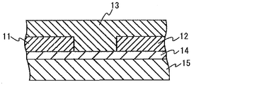
- a specific structure example of a field effect transistor is shown in FIG. In FIG.
- 11 is a source electrode
- 12 is a drain electrode
- 13 is a semiconductor layer
- 14 is a gate insulating layer
- 15 is a gate electrode also serving as a substrate.
- the field effect transistor shown in FIG. 2 is configured as a bottom contact / bottom gate transistor in which a source electrode, a drain electrode, and a gate electrode are closer to the substrate than the semiconductor layer.
- each member and each layer of the field effect transistor will be described.
- the field effect transistor is preferably supported on a substrate.
- Specific examples of the substrate include the same examples as the specific examples of the substrate in the organic electroluminescence element.
- gate electrode The constituent material of the gate electrode is not particularly limited as long as it is a conductive material, and any known material can be selected and used.
- gate electrode materials include platinum, gold, aluminum, chromium, nickel, copper, titanium, magnesium, calcium, barium, metals such as sodium, INO2, SnO 2, conductive metal oxides such as ITO, camphorsulfonic Conductive polymer with doped conductive polymer such as polyaniline doped with acid, polyethylenedioxythiophene doped with para-toluenesulfonic acid, and carbon black, graphite powder, metal fine particles etc. dispersed in binder A composite material etc. are mentioned.
- n-type impurities include Group 15 elements such as phosphorus (P) and arsenic (As).
- the thickness of the gate electrode is not particularly limited, but is preferably 0.01 ⁇ m or more, particularly 0.02 ⁇ m or more, and usually 2 ⁇ m or less, particularly 1 ⁇ m or less.
- the gate insulating layer is a layer having a function of maintaining an overlapping region between the gate electrode, the source electrode, and the drain electrode and a channel region on the gate electrode as an electrically insulating region.
- electrical insulation means that the electric conductivity is 10 ⁇ 9 S / cm or less.
- the material of the gate insulating layer is not particularly limited as long as it is an insulating material.
- any one of these materials may be used alone, or two or more of these materials may be used in any ratio and combination.
- a silicon substrate is used as the substrate, a SiO 2 layer formed by thermally oxidizing the silicon substrate may be used as the gate insulating layer.
- the electric conductivity at room temperature is usually 10 ⁇ 9 S / cm or less, particularly 10 ⁇ 14 S / cm.
- the following is preferable.
- the relative dielectric constant is usually 2.0 or more, preferably 2.5 or more.
- the thickness of the gate insulating layer is preferably 0.01 ⁇ m or more, particularly 0.1 ⁇ m or more, more preferably 0.2 ⁇ m or more, and usually 4 ⁇ m or less, especially 2 ⁇ m or less, and more preferably 1 ⁇ m or less.
- the constituent material of the semiconductor layer may be an organic semiconductor or an inorganic semiconductor.
- An oxide semiconductor is preferably used as the inorganic semiconductor.
- the organic semiconductor is preferably an n-type organic semiconductor.
- n-type organic semiconductors include fullerene (C60, C70, C76), octaazaporphyrin, p-type organic semiconductor perfluoro, naphthalene tetracarboxylic acid anhydride, naphthalene tetracarboxylic acid diimide, perylene tetracarboxylic acid anhydride, Examples thereof include aromatic carboxylic acid anhydrides such as perylenetetracarboxylic acid diimide, imidized products thereof, and derivatives containing these compounds as a skeleton.
- the preferable range and specific example of the p-type organic semiconductor used as a perfluoro body the preferable range and specific example of the p-type organic semiconductor used with the below-mentioned solar cell can be referred.
- the oxide semiconductor include zinc oxide, nickel oxide, tin oxide, titanium oxide, vanadium oxide, indium oxide, strontium titanate, and an In—Ga—Zn—O-based compound.
- the preferable thickness of the organic semiconductor layer is usually 5 nm or more, particularly 10 nm or more, more preferably 30 nm or more, and usually 10 ⁇ m or less, especially 1 ⁇ m or less, and further 500 nm or less.
- the source electrode and the drain electrode are constituted by the electrodes of the present invention. Since the electrode of the present invention has a small work function, the source electrode and the drain electrode can be efficiently injected into the semiconductor layer by configuring the source electrode and the drain electrode with the electrode of the present invention. The contact state of the drain electrode can be ohmic contact. As a result, the driving voltage is lowered and good voltage-current characteristics can be obtained.
- the work function of the electrodes used for the source electrode and the drain electrode of the transistor if the semiconductor layer bonded to the these electrodes is an organic semiconductor layer, and the absolute value E LUMO of the LUMO level of the organic semiconductor layer E LUMO ⁇ 1.5 eV, more preferably E LUMO ⁇ 1.0 eV, and even more preferably E LUMO ⁇ 0.5 eV.
- the work functions of the electrodes used for the source electrode and the drain electrode of the transistor are determined from the electron affinity of the inorganic semiconductor layer, that is, the bottom of the conduction band, when the semiconductor layer bonded to these electrodes is an inorganic semiconductor layer.
- the energy up to the vacuum level is ⁇ , it is preferably ⁇ ⁇ 1.5 eV, more preferably ⁇ ⁇ 1.0 eV, and even more preferably ⁇ ⁇ 0.5 eV.
- the work functions of the electrodes used for the source electrode and the drain electrode are particularly preferably equal to or lower than the work functions of the semiconductor layer bonded to these electrodes.
- the thicknesses of the source electrode and the drain electrode are not particularly limited, but are preferably 0.01 ⁇ m or more, particularly 0.02 ⁇ m or more, and usually 2 ⁇ m or less, especially 1 ⁇ m or less.
- An organic electric field transistor performs switching or amplification operation by controlling a current in a channel portion sandwiched between a source electrode and a drain electrode by a gate electrode.
- the channel width (the width between the source electrode and the drain electrode) is large in that it allows a large current to flow.
- the channel width is too large, the area of the element increases, which is disadvantageous in terms of integration. It may become. Note that a long channel length can be obtained by using a comb electrode as the source electrode and the drain electrode.
- the channel length is preferably 100 nm or more, particularly 500 nm or more, more preferably 1 ⁇ m or more, and usually 1 mm or less, especially 100 ⁇ m or less, and more preferably 50 ⁇ m or less.
- the width of the channel is preferably in the range of usually 500 nm or more, especially 5 ⁇ m or more, more preferably 10 ⁇ m or more, and usually 20 mm or less, especially 5 mm or less, more preferably 1 mm or less.
- the solar cell of the present invention has at least an anode, a cathode, and a structure in which a power generation layer is formed between the anode and the cathode, and the cathode is preferably composed of the electrode of the present invention.
- the power generation layer includes at least a photoelectric conversion layer, may be composed of only a photoelectric conversion layer, or may have one or more functional layers in addition to the photoelectric conversion layer. Examples of such other functional layers include a hole extraction layer, a hole transport layer, an electron blocking layer, a hole blocking layer, an electron transport layer, and an electron extraction layer.
- 21 is a substrate
- 22 is a cathode
- 23 is an electron extraction layer
- 24 is a photoelectric conversion layer
- 25 is a hole extraction layer
- 26 is an anode.
- the solar cell of the present invention is preferably supported by a substrate.
- a substrate the thing similar to the specific example of the board
- a metal foil or a laminate of a metal foil and a resin film can also be used as the substrate.
- the cathode has a function of taking out electrons from the power generation layer.
- the cathode is constituted by the electrode of the present invention. Since the electrode of the present invention has a small work function, the difference between the work function of the cathode and the work function of the anode is increased by forming the cathode with the electrode of the present invention, and a high open circuit voltage can be obtained.
- the contact state between the cathode and the semiconductor layer in the solar cell shown in FIG. 3, the electron extraction layer 23) can be ohmic contact, electrons from the semiconductor layer can be efficiently extracted to the cathode. Thereby, high energy conversion efficiency can be obtained.
- the work function of the electrode used for the cathode of the solar cell is E LUMO when the absolute value of the LUMO level of the organic semiconductor layer is E LUMO.
- LUMO ⁇ 1.5 eV is preferred, E LUMO ⁇ 1.0 eV is more preferred, and E LUMO ⁇ 0.5 eV is even more preferred.
- the work function of the electrode used for the cathode of the solar cell is as follows.
- the semiconductor layer bonded to the cathode is an inorganic semiconductor layer, the electron affinity of the inorganic semiconductor layer, that is, from the bottom of the conduction band to the vacuum level.
- the work function of the electrode used for the cathode of the solar cell is preferably equal to or lower than the work function of the semiconductor layer bonded to the cathode.
- the anode has a function of taking out holes from the power generation layer. It is preferable to use a conductive transparent material having a large work function for the anode. Specific examples of the conductive material used for the anode include the same materials as the specific examples of the anode in the organic electroluminescence element.
- the photoelectric conversion layer is a layer that converts light energy into electric energy.
- Examples of the material used for the photoelectric conversion layer include thin film single crystal silicon, thin film polycrystalline silicon, amorphous silicon, microcrystalline silicon, spherical silicon, an inorganic semiconductor, an organic dye, and an organic semiconductor.
- the photoelectric conversion layer may be a multi-junction type such as a stack type, a stacked type, or a tandem type.
- the inorganic semiconductor is preferably a chalcogenide-based semiconductor containing a chalcogen element such as S, Se, or Te, more preferably a group I-III-VI2 semiconductor (chalcopyrite system), and a group I element
- a Cu-III-VI2 group semiconductor using Cu as a CIS-based semiconductor [CuIn (Se1-ySy) 2; 0 ⁇ y ⁇ 1] or a CIGS-based semiconductor [Cu (In1-xGax) (Se1). ⁇ ySy) 2; 0 ⁇ x ⁇ 1, 0 ⁇ y ⁇ 1]] is particularly preferable.
- the photoelectric conversion layer is composed of an organic semiconductor, a bulk heterojunction type having a layer (i layer) in which a p-type organic semiconductor and an n-type organic semiconductor are phase-separated in the layer, and a layer (p layer) including a p-type organic semiconductor; It is preferable to use a laminated type (hetero pn junction type) in which layers (n layers) including an n-type organic semiconductor are laminated, a PIN type, a Schottky type, or a combination of these, and in particular, a bulk hetero junction type. Is more preferable.
- a ⁇ -conjugated polymer material As the p-type organic semiconductor, a ⁇ -conjugated polymer material, a ⁇ -conjugated low molecular organic compound, or the like can be preferably used.
- the conjugated polymer material is obtained by polymerizing single or plural kinds of ⁇ -conjugated monomers.
- ⁇ -conjugated monomers thiophene, fluorene, carbazole, diphenylthiophene, dithienothiophene, dithienosilole, dithienocyclohexane, benzothiadiazole, thienothiophene, imidothiophene, benzodithiophene, and derivatives containing these compounds as a skeleton Etc.
- Low molecular organic semiconductor materials include condensed aromatic hydrocarbons such as pentacene and naphthacene, oligothiophenes having four or more thiophene rings, porphyrin compounds, tetrabenzoporphyrin compounds and their metal complexes, phthalocyanine compounds and their metal complexes, etc. Is mentioned.
- n-type semiconductor compounds include fullerenes (C60, C70, C76), octaazaporphyrins, perfluoro compounds of the above p-type organic semiconductors, naphthalenetetracarboxylic acid anhydride, naphthalenetetracarboxylic acid diimide, and perylenetetracarboxylic acid anhydride.
- aromatic carboxylic acid anhydrides such as perylenetetracarboxylic acid diimide, imidized products thereof, and derivatives containing these compounds as a skeleton.
- the electron extraction layer is a layer that facilitates electron injection into the cathode.
- the material for the electron extraction layer include alkali metal salts such as LiF, n-type oxide semiconductors such as titanium oxide (TiOx) and zinc oxide (ZnO).
- the hole extraction layer is a layer that facilitates hole injection into the anode.
- a conductive polymer in which polythiophene, polypyrrole, polyaniline, or the like is doped with sulfonic acid, halogen, or the like, or a metal oxide having a high work function such as molybdenum oxide or nickel oxide can be used.
- the material constituting the photoelectric conversion layer is excited to generate charges.
- holes are transported to the positive electrode side and taken out to the anode, and electrons are transported to the cathode side and taken out to the cathode, and an electromotive force is generated between the anode and the cathode.
- a current flowing from the anode to the cathode can be obtained by connecting a conductor between the anode where the electromotive force is generated and the cathode.
- each layer and each member constituting the element of the present invention is not particularly limited, and either a dry process or a wet process may be used.
- the lithography method can be used.
- specific methods and steps reference can be made to the description of the lithography method in the method for producing a structure of the present invention, specific methods and steps.
- the reflectance was measured using a 1280 type tabletop thin film analyzer (n & k), and the work function was measured using a photoelectron spectrometer (AC-2) manufactured by Riken Keiki Co., Ltd.
- the output characteristics of the transistor were measured using a semiconductor parameter analyzer (manufactured by Agilent Technologies: HP4155) in an inert atmosphere having an oxygen concentration and a water concentration of 1 ppm or less.
- the light emitting area of the organic electroluminescence element was measured using an organic EL reliability evaluation apparatus evaluation and measurement apparatus EAS-26B (System Giken). Further, the alloy layer was formed by a vacuum evaporation method at a vacuum degree of 1 ⁇ 10 ⁇ 4 Pa or less by a co-evaporation method using a separate evaporation source for each constituent element.
- Example 1 Production and Evaluation of Electrode Consisting of MgCa Alloy
- An MgCa film having a thickness of 50 nm was formed on a glass substrate by a vacuum vapor deposition method to obtain an electrode.
- the Ca concentration was 6 atomic% or 25 atomic%, and two types of MgCa layers were formed.
- an Al layer, an MgAu layer, and an Mg layer were each formed to a thickness of 50 nm on a glass substrate by vacuum deposition.
- the concentration of Au in the MgAu layer was 10 atomic%.
- FIG. 4 shows the reflectance spectrum of each layer produced. In FIG.
- Mg94Ca6 represents an MgCa layer containing 6 atomic% of Ca
- Mg75Ca25 represents an MgCa layer containing 25 atomic% of Ca. As shown in FIG. 4, the MgCa layer had a high reflectance in the visible region regardless of whether the Ca concentration was low or high.
- Example 2 Production and Evaluation of Structure Made of MgCa Alloy
- a comb-shaped MgCa layer was produced by photolithography on a silicon substrate with an oxide film as described below to obtain a structure.
- surface treatment was performed with hexamethyldisilazane (HMDS).
- HMDS hexamethyldisilazane
- a lift-off layer forming solution (Rohm and Haas Co., Ltd .: LOL1000) is applied onto the substrate by spin coating, and then baked at 150 ° C., and then a positive resist (Tokyo Ohka Kogyo Co., Ltd.) is applied.
- Co., Ltd .: TMSR-8900 was applied by spin coating and baked at 110 ° C.
- the positive resist is exposed through a quartz photomask having a reversal pattern with respect to the target pattern (comb pattern), and the exposed portion is removed with a developer (manufactured by Tokyo Ohka Kogyo Co., Ltd .: NMD-3).
- a resist film patterned in a reverse pattern was obtained.
- an MgCa alloy was formed on the glass or silicon oxide-coated silicon or quartz substrate by a vacuum deposition method so as to cover the resist mask, thereby forming an MgCa layer having a thickness of 50 nm.
- the concentration of Ca in the MgCa alloy was 10 atomic%.
- FIG. 5 is a graph in which the irradiation light energy of ultraviolet rays is plotted on the horizontal axis and the photoelectron yield 0.5 power (square root) is plotted on the vertical axis.
- “0h”, “6h”, and “24h” represent sample storage (atmosphere) time from the completion of the process to the measurement of the electron yield. From FIG. 5, the work function of the MgCa layer of this comb pattern is 3.6 eV, which is a very small value.
- Example 3 Production and evaluation of organic transistor using MgCa alloy as source electrode and drain electrode Heavy doped n + -Si wafer (hereinafter referred to as a thermal oxide film (SiO 2 ) having a thickness of 300 nm as an insulating layer) And “n + -Si substrate”).
- a thermal oxide film SiO 2
- the n + -Si substrate was used as a substrate
- the n + region was used as a gate electrode
- a thermal oxide film was used as a gate insulating layer.
- a comb-shaped MgCa layer was formed on the n + -Si substrate in the same procedure as in Example 2.
- the Ca concentration in the MgCa alloy is set to 10 atomic%, and the resist film and the MgCa layer immediately above the resist film are peeled off using a remover solution (Rohm and Haas Co., Ltd .: Micro positremover 116) and acetone. It was.
- the comb teeth alternately correspond to the source electrode and the drain electrode, respectively, and have a total of 20 electrode pairs. The distance between the source electrode and the drain electrode was 25 ⁇ m, and the channel width was 4 mm.
- a C60 (n-type semiconductor) film was formed on the n + -Si substrate by vacuum deposition so as to cover the source electrode and the drain electrode, thereby forming a C60 layer having a thickness of 50 nm.
- the deposition rate was 0.01 nm / s.
- a bottom-gate / bottom-contact transistor was manufactured.
- Comparative Example 1 Fabrication and Evaluation of Organic Transistor Using Au as Source and Drain Electrode A transistor was formed in the same manner as in Example 3 except that source electrode and drain electrode were formed using Au instead of MgCa alloy. Was made. The drain voltage-drain current characteristics of the manufactured transistor are shown on the right side of FIG. Looking at the right side of FIG. 6, the drain current could not be observed in this measured voltage range, and good output characteristics as shown in FIG. 6 could not be obtained. This is presumably because the energy barrier between the source and drain electrodes and the C60 layer is large and is in a Schottky contact.
- Example 4 Production and evaluation of organic electroluminescence device using MgCa alloy as cathode Cathodic thin film was deposited on glass substrate on which an anode made of indium tin oxide (ITO) having a thickness of 100 nm was formed. And at a vacuum degree of 1 ⁇ 10 ⁇ 4 Pa. Specifically, first, HATCN was formed to a thickness of 10 nm on ITO, and TrisPCz was formed to a thickness of 30 nm thereon. Next, mCBP and 4CzIPN were co-evaporated from different deposition sources to form a layer having a thickness of 30 nm as a light emitting layer. At this time, the concentration of 4CzIPN was 15% by weight.
- ITO indium tin oxide
- T2T was formed to a thickness of 10 nm
- BPyTP2 was formed thereon to a thickness of 55 nm.
- a quartz photomask having a pattern corresponding to the planar shape of the cathode was used, a cathode was formed in the same manner as in the source electrode and drain electrode formation process of Example 3 to obtain an organic electroluminescence element.
- the concentration of Ca in the MgCa alloy was 30 atomic%.
- Example 2 Production and evaluation of organic electroluminescence device using Al or MgAu alloy as cathode
- Al or MgAu alloy was used instead of MgCa alloy when forming the cathode.
- two types of organic electroluminescence elements having different cathode materials were produced.
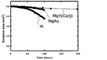
- the organic electroluminescent elements produced in Example 4 and Comparative Example 2 were left under conditions of room temperature of 25 ° C. and relative humidity of 50%, and the change with time of the size of the light emitting region was examined. The result is shown in FIG. As shown in FIG.
- the organic electroluminescence device having a cathode made of an MgCa alloy hardly changed the light emission area even when time passed, and kept a wide light emission area even after 200 hours passed. From this, it was confirmed that the electrode made of MgCa alloy was excellent in barrier properties.
- Example 5 Production and evaluation of electrode made of MgCa alloy, MgCaAg alloy or MgCaAl alloy
- an MgCa layer, MgCaAg layer or MgCaAl layer was formed on a glass substrate with a film thickness of 100 nm, respectively. It was.
- an Al layer having a thickness of 100 nm was formed on a glass substrate by a vacuum deposition method to form an electrode.
- Table 1 shows the composition ratio and work function of each layer produced. Moreover, the reflectance spectrum of each produced layer is shown in FIG.
- the composition of the alloy shown in FIG. 8 corresponds to the composition of the alloy shown in Table 1, and the numerical value represents the composition ratio in atomic%. The same applies to the alloy composition in the following description.
- the work functions of the MgCaAg alloy and the MgCaAl alloy were extremely small values as in the case of the MgCa alloy.
- the MgCa layer, the MgCaAg layer, and the MgCaAl layer all show a high reflectance in the visible light region.
- the MgCaAg layer and the MgCaAl layer are shorter than the MgCa layer in the short wavelength region of 450 nm or less. It can be seen that a high reflectance of 80% or more is exhibited. From this, it was found that by adding Ag or Al to the alloy as the third component, a high reflectance of 80% or more can be achieved in the entire visible light region.
- Example 6 Preparation and evaluation of organic electroluminescence device using MgCaAg alloy or MgCaAl alloy as cathode
- MgCa having the composition shown in Table 2 instead of the MgCa alloy having a Ca concentration of 30 atomic%
- Three types of organic electroluminescence elements having different cathode materials were produced in the same manner as in Example 4 except that an alloy, MgCaAg alloy, and MgCaAl alloy were used.
- the produced organic electroluminescence device was left standing under conditions of room temperature 25 ° C. and relative humidity 50%, and the change over time of the size of the light emitting region was examined.
- FIG. Table 2 shows the time to reach% (electrode life).
- the composition of the alloy shown in FIG. 9 corresponds to the alloy composition of the cathode shown in Table 2, and each indicates an organic electroluminescence element using the alloy as a cathode.
- the organic electroluminescence device using the MgCaAg alloy or MgCaAl alloy as the cathode decreases the emission region over time as compared with the organic electroluminescence device using the MgCa alloy as the cathode. It can be seen that is significantly suppressed. From this, it was found that the atmospheric stability of the electrode is greatly improved by adding Ag or Al as the third component to the electrode alloy. When the same test was performed on the Mg77Ca8Ag15 alloy layer, the same reflection characteristics and electrode life characteristics (atmospheric stability) as the Mg73Ca5Ag22 alloy layer were shown.
- Example 2 when the Mg73Ca5Ag22 alloy, the Mg77Ca8Ag15 alloy, or the Mg88Ca9Al3 alloy was formed in a comb pattern by the same method as in Example 2, a good pattern shape equivalent to the MgCa alloy in Example 2 was obtained. It was confirmed that the aptitude was very high. Further, using a Mg73Ca5Ag22 alloy, a Mg77Ca8Ag15 alloy, or a Mg88Ca9Al3 alloy as a source electrode material and a drain electrode material, a transistor was fabricated and the drain voltage-drain current characteristics were measured in the same manner as in Example 3. The same tendency as in Example 3 was observed. Thus, it was confirmed that each electrode and the C60 layer were in ohmic contact.
- Example 7 Preparation and evaluation of organic electroluminescence device in which Ca content of MgCa alloy constituting cathode is changed.
- a cathode instead of forming an MgCa layer having a Ca content of 30 atomic%, it is shown in Table 3. Except that the MgCa layer having the composition ratio was formed, the same steps as in Example 4 were performed to prepare eight types of organic electroluminescence elements having different Ca contents of the MgCa alloy constituting the cathode. Each of the produced organic electroluminescence elements was allowed to stand for 95 hours under conditions of a room temperature of 25 ° C. and a relative humidity of 40%, and the ratio (%) of the light emission area after 95 hours to the initial light emission area was determined.
- the electrode shape was observed with a microscope when 48 hours passed and 95 hours passed, and durability was evaluated according to the following criteria.
- Durability evaluation by electrode shape ⁇ : The electrode shape is maintained at the time of 95 hours.
- an MgCa layer was formed at the same composition ratio as the cathode of each organic electroluminescence element, and the work function and the reflectance of 450 nm wavelength light were examined. Further, the reflectance was evaluated according to the following criteria.
- the organic electroluminescence device using the MgCa layer as the cathode has a light emitting area ratio with respect to the initial value at the time of 95 hours higher than 86% of the standard device, and maintains the electrode shape at the time of 95 hours, Excellent durability.
- the MgCa layer having a Ca content of 18 atomic% or less has a high reflectance of 80% or more, and the reflected light can contribute to improving the light extraction efficiency of the device.
- the organic electroluminescence device using the MgCa layer with a Ca content of 4 atomic% as the cathode has a light emitting area ratio with respect to the initial value after the lapse of 95 hours, which is less than 86% of the standard device. It was inferior to.
- the organic electroluminescence device using the MgCa layer having a Ca content of 31 atomic% as the cathode had an electrode deformed after 95 hours and was also inferior in durability. From the above results, it was found that the Ca content of the MgCa alloy needs to be 5 to 30 atomic% in order to realize a highly durable device using the electrode having the MgCa alloy.
- the electrode of the present invention has a low work function, can be brought into ohmic contact with the semiconductor layer, has high lithography suitability, and is excellent in weather resistance and a barrier against oxygen and water vapor. For this reason, by using the electrode of the present invention, a driving voltage is low, good element characteristics are obtained, and an element having excellent durability can be realized. For this reason, this invention has high industrial applicability.
Landscapes
- Chemical & Material Sciences (AREA)
- Engineering & Computer Science (AREA)
- Materials Engineering (AREA)
- Mechanical Engineering (AREA)
- Metallurgy (AREA)
- Organic Chemistry (AREA)
- Manufacturing & Machinery (AREA)
- Electrodes Of Semiconductors (AREA)
Abstract
MgCa(X)nで表される合金を有する電極。nは0または1を表す。nが0であるとき、Caの含有量が5~30原子%である。nが1であるとき、XはAg、Al、Cr、Cu、ZnおよびLiから選択される1以上の原子を表し、Mgの含有量が50~95原子%であり、Caの含有量が1~50原子%であり、Agの含有量が0.1~30原子%である。この発明によれば、仕事関数が低く、半導体層に対してオーミック接触させることができ、さらに、高いリソグラフィー適性を有し、耐候性およびバリア性に優れた電極を実現しうる。
Description
本発明は、半導体に効率よく電子を注入することができる電極、構造体および接続構造体に関する。また、その電極を用いた素子にも関する。
トランジスタや有機発光素子などの半導体素子は、半導体層に金属電極が接続された構造を有し、金属電極と半導体層の間の電荷移動を経て動作するように構成されている。
例えば、電界効果型のトランジスタは、分離して設けられたソース電極およびドレイン電極と、ソース電極とドレイン電極の間に、各電極と接触して設けられた半導体層と、この半導体層に重なるように、ゲート絶縁層を介して設けられたゲート電極とを有して構成されている。こうしたトランジスタでは、ドレイン電極とソース電極の間に電位差を生じさせた状態で、ゲート電極に信号電圧を印加すると、半導体層に電荷の流路(チャネル)が形成され、ソース電極-ドレイン電極間を電流が流れる。これにより、トランジスタは、例えばドレイン電極に接続された素子のオン・オフを制御するスイッチング素子や電流増幅素子として機能する。
こうした半導体素子の電極材料としては、これまで金が最も多く用いられている(例えば、特許文献1~3参照)。これは、金が化学的に安定であるとともに、真空蒸着を用いて容易に成膜することができ、また、フォトレジストを用いたリフトオフ法により微細加工が可能であるためである。
例えば、電界効果型のトランジスタは、分離して設けられたソース電極およびドレイン電極と、ソース電極とドレイン電極の間に、各電極と接触して設けられた半導体層と、この半導体層に重なるように、ゲート絶縁層を介して設けられたゲート電極とを有して構成されている。こうしたトランジスタでは、ドレイン電極とソース電極の間に電位差を生じさせた状態で、ゲート電極に信号電圧を印加すると、半導体層に電荷の流路(チャネル)が形成され、ソース電極-ドレイン電極間を電流が流れる。これにより、トランジスタは、例えばドレイン電極に接続された素子のオン・オフを制御するスイッチング素子や電流増幅素子として機能する。
こうした半導体素子の電極材料としては、これまで金が最も多く用いられている(例えば、特許文献1~3参照)。これは、金が化学的に安定であるとともに、真空蒸着を用いて容易に成膜することができ、また、フォトレジストを用いたリフトオフ法により微細加工が可能であるためである。
しかしながら、金は仕事関数がおよそ4.9eV程度と高いために、金電極を半導体層に接続すると、電極の仕事関数と半導体層の電子親和力との差に相当するエネルギー障壁が高くなって電極から半導体層への電子注入効率が低くなることや、電極の仕事関数が半導体層の仕事関数よりも大きくなって電極と半導体層との接触がショットキー接触になることにより、素子の駆動電圧が高くなる傾向がある。また、トランジスタの場合では、低電圧領域では、電極から半導体層へ電流がほとんど流れず、印加電圧が一定の値に達すると、急に大きな電流が半導体層へ流れるという現象が見られ、良好な電圧電流特性が得られないという問題も生じている。
このような状況下において、本発明者らは、仕事関数が低く、半導体層に対してオーミック接触させることができ、さらに、高いリソグラフィー適性を有する電極、構造体および接続構造体を提供することを目的として鋭意検討を進めた。また、こうした電極を用いることにより、駆動電圧が低く、良好な特性が得られる素子を提供することを目的として鋭意検討を進めた。
上記の目的を達成するために、本発明者らが様々な金属や合金で電極を形成して半導体層と接続し、その電圧電流特性を評価する検討を網羅的に行ったところ、驚くべきことに、MgとCaを含む合金を有する電極と半導体層とを接続した場合に、その電圧電流曲線が原点を通って一次関数的に増大するという理想的な結果が得られ、オーミック接触が実現するという知見を得るに至った。さらに、MgCa電極については、そのCa含有量を特定の範囲に規定することにより、電極の耐候性が向上し、その電極を適用した素子の耐久性が改善されるとの知見も得た。本発明者らは、これらの知見に基づいて提案されたものであり、具体的に、以下の構成を有する。
[1] 下記一般式(1)で表される合金を有する電極。
一般式(1)
MgCa(X)n
[一般式(1)において、nは0または1を表す。nが0であるとき、前記合金に含まれるCaの含有量が合金全原子数の5~30原子%である。nが1であるとき、XはAg、Al、Cr、Cu、ZnおよびLiから選択される1以上の原子を表し、前記合金に含まれるMgの含有量が合金全原子数の50~95原子%であり、前記合金に含まれるCaの含有量が合金全原子数の1~50原子%であり、前記合金に含まれるAgの含有量が合金全原子数の0.1~30原子%である。]
[2] nが0である、[1]に記載の電極。
[3] 前記合金に含まれるCaの含有量が合金全原子数の5~18原子%である、[2]に記載の電極。
[4] nが1である、[1]に記載の電極。
[5] XがAgおよびAlから選択される1以上の原子である、[1]に記載の電極。
[6] 前記合金の仕事関数が4.0eV以下である、[1]~[5]のいずれか1項に記載の電極。
一般式(1)
MgCa(X)n
[一般式(1)において、nは0または1を表す。nが0であるとき、前記合金に含まれるCaの含有量が合金全原子数の5~30原子%である。nが1であるとき、XはAg、Al、Cr、Cu、ZnおよびLiから選択される1以上の原子を表し、前記合金に含まれるMgの含有量が合金全原子数の50~95原子%であり、前記合金に含まれるCaの含有量が合金全原子数の1~50原子%であり、前記合金に含まれるAgの含有量が合金全原子数の0.1~30原子%である。]
[2] nが0である、[1]に記載の電極。
[3] 前記合金に含まれるCaの含有量が合金全原子数の5~18原子%である、[2]に記載の電極。
[4] nが1である、[1]に記載の電極。
[5] XがAgおよびAlから選択される1以上の原子である、[1]に記載の電極。
[6] 前記合金の仕事関数が4.0eV以下である、[1]~[5]のいずれか1項に記載の電極。
[7] 前記一般式(1)で表される合金からなり、表面に500nm~200μmのピッチを有する凹凸を有する構造体。
[8] 前記合金からなる複数の帯状体が、500nm~200μmのピッチで並列した構造を有する、[7]に記載の構造体。
[8] 前記合金からなる複数の帯状体が、500nm~200μmのピッチで並列した構造を有する、[7]に記載の構造体。
[9] 前記一般式(1)で表される合金をリソグラフィー法により成形する工程を含む、構造体の製造方法。
[10] 前記工程が、前記合金の表面にリソグラフィー法により凹凸を形成する工程である、[9]に記載の構造体の製造方法。
[11] 前記工程が、前記合金をリフトオフ法により成形する工程を含む、[9]に記載の構造体の製造方法。
[12] 前記リソグラフィー法がフォトリソグラフィー法である、[9]~[11]のいずれか1項に記載の構造体の製造方法。
[13] 前記合金が、基板上に形成された合金膜である、[9]~[12]のいずれか1項に記載の構造体の製造方法。
[14] 前記合金膜をスパッタリング法により形成する、[13]に記載の構造体の製造方法。
[10] 前記工程が、前記合金の表面にリソグラフィー法により凹凸を形成する工程である、[9]に記載の構造体の製造方法。
[11] 前記工程が、前記合金をリフトオフ法により成形する工程を含む、[9]に記載の構造体の製造方法。
[12] 前記リソグラフィー法がフォトリソグラフィー法である、[9]~[11]のいずれか1項に記載の構造体の製造方法。
[13] 前記合金が、基板上に形成された合金膜である、[9]~[12]のいずれか1項に記載の構造体の製造方法。
[14] 前記合金膜をスパッタリング法により形成する、[13]に記載の構造体の製造方法。
[15] 前記一般式(1)で表される合金と半導体が電気的に接続した構造を有する、接続構造体。
[16] 前記半導体が有機半導体である、[15]に記載の接続構造体。
[17] 前記半導体が酸化物半導体である、[15]に記載の接続構造体。
[18] 前記合金と前記半導体がオーミック接触している、[15]~[17]のいずれか1項に記載の接続構造体。
[16] 前記半導体が有機半導体である、[15]に記載の接続構造体。
[17] 前記半導体が酸化物半導体である、[15]に記載の接続構造体。
[18] 前記合金と前記半導体がオーミック接触している、[15]~[17]のいずれか1項に記載の接続構造体。
[19] [1]~[6]のいずれか1項に記載の電極を有する素子。
[20] 前記素子が、前記電極と半導体が電気的に接続した構造を有する、[19]に記載の素子。
[21] 前記素子が有機発光素子、太陽電池、またはトランジスタである、[19]または[20]に記載の素子。
[22] 前記素子が有機トランジスタである、[21]に記載の素子。
[23] 前記素子が酸化物トランジスタである、[21]に記載の素子。
[20] 前記素子が、前記電極と半導体が電気的に接続した構造を有する、[19]に記載の素子。
[21] 前記素子が有機発光素子、太陽電池、またはトランジスタである、[19]または[20]に記載の素子。
[22] 前記素子が有機トランジスタである、[21]に記載の素子。
[23] 前記素子が酸化物トランジスタである、[21]に記載の素子。
本発明の電極は、仕事関数が小さいため、半導体層と接続したときに、電極から半導体層への電子注入に対するエネルギー障壁が低く、半導体層へ効率よく電子を注入することができるとともに、電極と半導体層との接触状態をオーミック接触にすることができる。また、本発明の電極は高いリソグラフィー適性を有しており、リソグラフィー法を用いて精密に微細加工することができる。さらに、本発明の電極は、耐候性に優れており、酸素や水蒸気に対してバリア性を示す。本発明の素子は、こうした電極を用いるため、駆動電圧が低く、良好な特性が得られ、高い耐久性を有する。
以下において、本発明の内容について詳細に説明する。以下に記載する構成要件の説明は、本発明の代表的な実施態様や具体例に基づいてなされることがあるが、本発明はそのような実施態様や具体例に限定されるものではない。なお、本明細書において「~」を用いて表される数値範囲は、「~」の前後に記載される数値を下限値および上限値として含む範囲を意味する。また、本発明に用いられる化合物の分子内に存在する水素原子の同位体種は特に限定されず、例えば分子内の水素原子がすべて1Hであってもよいし、一部または全部が2H(デューテリウムD)であってもよい。また、本明細書中におけるMg、Ca、Xで表される原子、一般式(1)で表される合金以外の材料の各含有量(原子%)は、エネルギー分散型X線分析装置により測定されるものである。
(1)電極
本発明の電極は、下記一般式(1)で表される合金を有することを特徴とする。
一般式(1)
MgCa(X)n
一般式(1)において、nは0または1を表す。nが0であるとき、合金に含まれるCaの含有量が合金全原子数の5~30原子%である。nが1であるとき、XはAg、Al、Cr、Cu、ZnおよびLiから選択される1以上の原子を表し、前記合金に含まれるMgの含有量が合金全原子数の50~95原子%であり、前記合金に含まれるCaの含有量が合金全原子数の1~50原子%であり、前記合金に含まれるAgの含有量が合金全原子数の0.1~30原子%である。
一般式(1)において、nが0であるとき、一般式(1)で表される合金は、MgとCaのみを合金成分とする合金を意味する。以下の説明では、nが0である場合の一般式(1)で表される合金をMgCa合金という。MgCa合金におけるCaの含有量は、合金全原子数の5~30原子%であり、その残部がMgの含有量である。
一般式(1)において、nが1であるとき、一般式(1)で表される合金は、MgおよびCaと、Xで表される原子を合金成分とする合金を意味する。以下の説明では、nが1である場合の一般式(1)で表される合金をMgCaX合金という。XはAg、Al、Cr、Cu、ZnおよびLiから選択される1以上の原子であり、1種類の原子であっても2種類以上の原子であってもよい。MgCaX合金の各原子の含有量は特に制限されず、その3種類以上の原子が合金に含まれていて、合計で100原子%になっていればよい。
なお、上記の「MgとCaのみを合金成分とする合金」、「MgおよびCaと、Xで表される原子を合金成分とする合金」は、合金が不可避的な不純物元素を含むことを排除するものではない。「不可避的な不純物元素」とは、合金における含有量が1原子%以下の元素のことをいい、含有量は0.1原子%以下であることが好ましく、0.01原子%以下であることがより好ましく、0.001原子%以下であることがさらに好ましい。
本発明で用いる一般式(1)で表される合金は仕事関数が4eV以下の低い水準にある。このため、一般式(1)で表される合金を有する電極は、電極と半導体層との接続構造において、電極から半導体層への電子注入に対するエネルギー障壁が低く、半導体層へ効率よく電子を注入することができるとともに、半導体層との接触状態をオーミック接触にすることができる。これにより、この電極を用いる素子の駆動電圧を低くして、良好な素子特性を実現することができる。
また、一般式(1)で表される合金は、気相プロセスを用いて容易に成膜できるとともに、その合金膜は、リソグラフィー法を用いて精密に微細加工することができ、特に、リフトオフ法による微細加工に適している。さらに、この合金膜の構成元素であるMgおよびCaは、Auのような希少元素ではないために安価である。このため、一般式(1)で表される合金で電極を構成することにより、素子の製造コストを削減することができる。
また、一般式(1)で表される合金は酸素や水蒸気に対するバリア性に優れており、この合金を電極に用いることにより、素子の耐候性を向上させることができる。これにより、バリア性が高い高価なガスバリアフィルムに替えて、バリア性が比較的低い安価なガスバリアフィルムを用いることができるため、素子の製造コストをさらに削減することが可能になる。
さらに、また、一般式(1)で表される合金は可視領域の光に対して反射率が高い。このため、この合金を、例えば発光素子の光取出し側と反対側に配される電極に用いた場合には、発光層から光取出し側と反対側に放射された光が電極で効率よく反射され、光取出し側から効率よく取り出すことができる。これにより、高い発光効率を得ることができる。
以下において、一般式(1)で表される合金の組成について、nが0である場合と、nが1である場合のそれぞれについて説明する。
本発明の電極は、下記一般式(1)で表される合金を有することを特徴とする。
一般式(1)
MgCa(X)n
一般式(1)において、nは0または1を表す。nが0であるとき、合金に含まれるCaの含有量が合金全原子数の5~30原子%である。nが1であるとき、XはAg、Al、Cr、Cu、ZnおよびLiから選択される1以上の原子を表し、前記合金に含まれるMgの含有量が合金全原子数の50~95原子%であり、前記合金に含まれるCaの含有量が合金全原子数の1~50原子%であり、前記合金に含まれるAgの含有量が合金全原子数の0.1~30原子%である。
一般式(1)において、nが0であるとき、一般式(1)で表される合金は、MgとCaのみを合金成分とする合金を意味する。以下の説明では、nが0である場合の一般式(1)で表される合金をMgCa合金という。MgCa合金におけるCaの含有量は、合金全原子数の5~30原子%であり、その残部がMgの含有量である。
一般式(1)において、nが1であるとき、一般式(1)で表される合金は、MgおよびCaと、Xで表される原子を合金成分とする合金を意味する。以下の説明では、nが1である場合の一般式(1)で表される合金をMgCaX合金という。XはAg、Al、Cr、Cu、ZnおよびLiから選択される1以上の原子であり、1種類の原子であっても2種類以上の原子であってもよい。MgCaX合金の各原子の含有量は特に制限されず、その3種類以上の原子が合金に含まれていて、合計で100原子%になっていればよい。
なお、上記の「MgとCaのみを合金成分とする合金」、「MgおよびCaと、Xで表される原子を合金成分とする合金」は、合金が不可避的な不純物元素を含むことを排除するものではない。「不可避的な不純物元素」とは、合金における含有量が1原子%以下の元素のことをいい、含有量は0.1原子%以下であることが好ましく、0.01原子%以下であることがより好ましく、0.001原子%以下であることがさらに好ましい。
本発明で用いる一般式(1)で表される合金は仕事関数が4eV以下の低い水準にある。このため、一般式(1)で表される合金を有する電極は、電極と半導体層との接続構造において、電極から半導体層への電子注入に対するエネルギー障壁が低く、半導体層へ効率よく電子を注入することができるとともに、半導体層との接触状態をオーミック接触にすることができる。これにより、この電極を用いる素子の駆動電圧を低くして、良好な素子特性を実現することができる。
また、一般式(1)で表される合金は、気相プロセスを用いて容易に成膜できるとともに、その合金膜は、リソグラフィー法を用いて精密に微細加工することができ、特に、リフトオフ法による微細加工に適している。さらに、この合金膜の構成元素であるMgおよびCaは、Auのような希少元素ではないために安価である。このため、一般式(1)で表される合金で電極を構成することにより、素子の製造コストを削減することができる。
また、一般式(1)で表される合金は酸素や水蒸気に対するバリア性に優れており、この合金を電極に用いることにより、素子の耐候性を向上させることができる。これにより、バリア性が高い高価なガスバリアフィルムに替えて、バリア性が比較的低い安価なガスバリアフィルムを用いることができるため、素子の製造コストをさらに削減することが可能になる。
さらに、また、一般式(1)で表される合金は可視領域の光に対して反射率が高い。このため、この合金を、例えば発光素子の光取出し側と反対側に配される電極に用いた場合には、発光層から光取出し側と反対側に放射された光が電極で効率よく反射され、光取出し側から効率よく取り出すことができる。これにより、高い発光効率を得ることができる。
以下において、一般式(1)で表される合金の組成について、nが0である場合と、nが1である場合のそれぞれについて説明する。
[nが0である場合の一般式(1)で表される合金の組成]
上記のように、本発明で用いる一般式(1)で表される合金は、nが0であるとき、MgとCaのみを合金成分とするMgCa合金であり、そのMgCa合金に含まれるCaの含有量は、合金全原子数の5~30原子%であり、その残部がMgの含有量である。Caの含有量を上記の範囲に規定したのは下記の理由による。
すなわち、MgCa合金の組成比をMg:Ca=1:1からCa組成比を下げて行くと、仕事関数が大きくなる傾向が見られることから、これまでは、Caの含有量が50原子%未満のMgCa合金は電極材料として有用性が低いと考えられていた。しかし、本発明者らが、Ca含有量を30原子%程度まで減らしたMgCa合金を作製し、その特性を評価したところ、仕事関数が4eV以下の低い水準にあるという、意外な発見をした。また、特にCa含有量が5~30原子%のMgCa合金は、耐候性に優れていて、酸素や水蒸気に対するバリア性を示し、その合金を電極に使用した素子において、経時的な性能劣化や電極形状の変形が抑えられることも判明した。本発明におけるMgCa合金のCa含有量は、こうした知見に基づいて規定されたものである。すなわち、本発明で用いるMgCa合金は、そのCa含有量が5~30原子%であることにより、仕事関数が低く、電極と半導体層との接続構造において、低いエネルギー障壁とオーミック接触を実現することができる。また、そのMgCa合金を素子の電極に用いることにより、素子に酸素や水蒸気に対するバリア性が付与されて、素子保管時の経時的な性能劣化や電極の変形が抑えられるようになる。さらに、素子に酸素や水蒸気に対するバリア性が付与されるため、特に、酸素や水に弱い有機エレクトロルミネッセンス素子等においても、10-6gm-2day-1レベルの高いバリア性を示す高価なガスバリアフィルムを用いなくても、よりバリア性が低い安価なガスバリアフィルム(10-4gm-2day-1レベル)を用いれば十分になる。その結果、こうした素子の製造コストを削減することが可能になる。
ここで、MgCa合金のCa含有量の好ましい範囲は、5~18原子%である。これにより、MgCa合金の反射率が高くなり、例えば、そのMgCa合金を有する電極を発光素子の光取出し側と反対側に配したとき、発光層が放射した光を電極で効率よく反射させて光取出し側で取り出すことができる。その結果、高い発光効率を得ることができる。また、さらに、MgCa合金のCa含有量の下限は、6原子%超であることが好ましく、9原子%以上であることがより好ましく、その上限は16原子%未満であることがより好ましく、12原子%以下であることがさらに好ましい。MgCa合金のCa含有量が、上記の下限で規定される範囲であることにより、素子保管時の性能劣化をより効果的に抑えることができる。また、MgCa合金のCa含有量が、上記の上限で規定される範囲であることにより、仕事関数がより低いものにすることができる。
上記のように、本発明で用いる一般式(1)で表される合金は、nが0であるとき、MgとCaのみを合金成分とするMgCa合金であり、そのMgCa合金に含まれるCaの含有量は、合金全原子数の5~30原子%であり、その残部がMgの含有量である。Caの含有量を上記の範囲に規定したのは下記の理由による。
すなわち、MgCa合金の組成比をMg:Ca=1:1からCa組成比を下げて行くと、仕事関数が大きくなる傾向が見られることから、これまでは、Caの含有量が50原子%未満のMgCa合金は電極材料として有用性が低いと考えられていた。しかし、本発明者らが、Ca含有量を30原子%程度まで減らしたMgCa合金を作製し、その特性を評価したところ、仕事関数が4eV以下の低い水準にあるという、意外な発見をした。また、特にCa含有量が5~30原子%のMgCa合金は、耐候性に優れていて、酸素や水蒸気に対するバリア性を示し、その合金を電極に使用した素子において、経時的な性能劣化や電極形状の変形が抑えられることも判明した。本発明におけるMgCa合金のCa含有量は、こうした知見に基づいて規定されたものである。すなわち、本発明で用いるMgCa合金は、そのCa含有量が5~30原子%であることにより、仕事関数が低く、電極と半導体層との接続構造において、低いエネルギー障壁とオーミック接触を実現することができる。また、そのMgCa合金を素子の電極に用いることにより、素子に酸素や水蒸気に対するバリア性が付与されて、素子保管時の経時的な性能劣化や電極の変形が抑えられるようになる。さらに、素子に酸素や水蒸気に対するバリア性が付与されるため、特に、酸素や水に弱い有機エレクトロルミネッセンス素子等においても、10-6gm-2day-1レベルの高いバリア性を示す高価なガスバリアフィルムを用いなくても、よりバリア性が低い安価なガスバリアフィルム(10-4gm-2day-1レベル)を用いれば十分になる。その結果、こうした素子の製造コストを削減することが可能になる。
ここで、MgCa合金のCa含有量の好ましい範囲は、5~18原子%である。これにより、MgCa合金の反射率が高くなり、例えば、そのMgCa合金を有する電極を発光素子の光取出し側と反対側に配したとき、発光層が放射した光を電極で効率よく反射させて光取出し側で取り出すことができる。その結果、高い発光効率を得ることができる。また、さらに、MgCa合金のCa含有量の下限は、6原子%超であることが好ましく、9原子%以上であることがより好ましく、その上限は16原子%未満であることがより好ましく、12原子%以下であることがさらに好ましい。MgCa合金のCa含有量が、上記の下限で規定される範囲であることにより、素子保管時の性能劣化をより効果的に抑えることができる。また、MgCa合金のCa含有量が、上記の上限で規定される範囲であることにより、仕事関数がより低いものにすることができる。
[nが1である場合の一般式(1)で表される合金の組成]
本発明で用いる一般式(1)で表される合金は、nが1であるとき、Mg、CaおよびXで表される原子を合金成分とするMgCaX合金である。MgCaX合金に含まれる各原子の含有量は、特に制限されないが、Mgの含有量は、好ましくは合金全原子数の50~95原子%であり、より好ましくは合金全原子数の70~95原子%である。
MgCaX合金のXが表す原子は、Ag、Al、Cr、Cu、ZnおよびLiから選択される1以上の原子であり、1種類の原子であっても2種類以上の原子の組み合わせであってもよい。MgCaX合金は、MgおよびCaの他に、Xで表される原子を含むことにより、電極の仕事関数を制御することや、導電率やバリア性を向上させることができる。また、Xが表す原子は、AgおよびAlから選択される1以上の原子であることが好ましい。AgおよびAlから選択される1以上の原子をXとするMgCaX合金の好ましい例として、MgCaAg合金、MgCaAl合金、MgCaAgAl合金を挙げることができる。
MgCaX合金において、Xで表される原子の含有量は、合金全原子数の0.1~30原子%であることが好ましく、1~30原子%であることがより好ましい。例えば下限値が1原子%以上、3原子%以上、5原子%以上の範囲から選択してもよいし、上限値が23原子%以下、16原子%以下、10原子%以下、6原子%以下の範囲から選択してもよい。MgCaX合金において、Caの含有量は、合金全原子数の1~50原子%であることが好ましく、3~50原子%であることがより好ましい。例えば下限値が2原子%以上、3原子%以上、5原子%以上の範囲から選択してもよいし、上限値が30原子%以下、20原子%以下、10原子%以下、6原子%以下の範囲から選択してもよい。また、CaとXで表される原子の合計含有量は、合金全原子数の5~50原子%であることが好ましく、10~30原子%であることがより好ましい。
また、Xで表される原子の含有量は、Ca原子数の0.2~5.0倍であることが好ましく、例えば下限値がCa原子数の0.3倍以上、0.6倍以上、1倍以上の範囲から選択してもよく、上限値がCa原子数の4.4倍以下、2倍以下、1.5倍以下の範囲から選択してもよい。
ここで、Xが2種類以上の原子の組み合わせを表す場合には、その合計の含有量が上記のXで表される原子の含有量に対応することとする。
一方、MgCaX合金におけるCaとMgの合計含有量は、例えば合金全原子数の70原子%以上、77原子%以上、84原子%以上、90原子%以上、95原子%以上、99原子%以上、99.9原子%以上の範囲から選択してもよい。
MgCaX合金の組成として、例えば、合金に含まれるMgの含有量が合金全原子数の50~95原子%であり、前記合金に含まれるCaの含有量が合金全原子数の1~50原子%であり、前記合金に含まれるXの含有量が合金全原子数の0.1~30原子%である組成や、あるいは、合金に含まれるMgの含有量が合金全原子数の50~95原子%であり、前記合金に含まれるCaの含有量が合金全原子数の3~50原子%であり、前記合金に含まれるXの含有量が合金全原子数の0.1~30原子%である組成などを好ましく選択することができる。
本発明で用いる一般式(1)で表される合金は、nが1であるとき、Mg、CaおよびXで表される原子を合金成分とするMgCaX合金である。MgCaX合金に含まれる各原子の含有量は、特に制限されないが、Mgの含有量は、好ましくは合金全原子数の50~95原子%であり、より好ましくは合金全原子数の70~95原子%である。
MgCaX合金のXが表す原子は、Ag、Al、Cr、Cu、ZnおよびLiから選択される1以上の原子であり、1種類の原子であっても2種類以上の原子の組み合わせであってもよい。MgCaX合金は、MgおよびCaの他に、Xで表される原子を含むことにより、電極の仕事関数を制御することや、導電率やバリア性を向上させることができる。また、Xが表す原子は、AgおよびAlから選択される1以上の原子であることが好ましい。AgおよびAlから選択される1以上の原子をXとするMgCaX合金の好ましい例として、MgCaAg合金、MgCaAl合金、MgCaAgAl合金を挙げることができる。
MgCaX合金において、Xで表される原子の含有量は、合金全原子数の0.1~30原子%であることが好ましく、1~30原子%であることがより好ましい。例えば下限値が1原子%以上、3原子%以上、5原子%以上の範囲から選択してもよいし、上限値が23原子%以下、16原子%以下、10原子%以下、6原子%以下の範囲から選択してもよい。MgCaX合金において、Caの含有量は、合金全原子数の1~50原子%であることが好ましく、3~50原子%であることがより好ましい。例えば下限値が2原子%以上、3原子%以上、5原子%以上の範囲から選択してもよいし、上限値が30原子%以下、20原子%以下、10原子%以下、6原子%以下の範囲から選択してもよい。また、CaとXで表される原子の合計含有量は、合金全原子数の5~50原子%であることが好ましく、10~30原子%であることがより好ましい。
また、Xで表される原子の含有量は、Ca原子数の0.2~5.0倍であることが好ましく、例えば下限値がCa原子数の0.3倍以上、0.6倍以上、1倍以上の範囲から選択してもよく、上限値がCa原子数の4.4倍以下、2倍以下、1.5倍以下の範囲から選択してもよい。
ここで、Xが2種類以上の原子の組み合わせを表す場合には、その合計の含有量が上記のXで表される原子の含有量に対応することとする。
一方、MgCaX合金におけるCaとMgの合計含有量は、例えば合金全原子数の70原子%以上、77原子%以上、84原子%以上、90原子%以上、95原子%以上、99原子%以上、99.9原子%以上の範囲から選択してもよい。
MgCaX合金の組成として、例えば、合金に含まれるMgの含有量が合金全原子数の50~95原子%であり、前記合金に含まれるCaの含有量が合金全原子数の1~50原子%であり、前記合金に含まれるXの含有量が合金全原子数の0.1~30原子%である組成や、あるいは、合金に含まれるMgの含有量が合金全原子数の50~95原子%であり、前記合金に含まれるCaの含有量が合金全原子数の3~50原子%であり、前記合金に含まれるXの含有量が合金全原子数の0.1~30原子%である組成などを好ましく選択することができる。
[合金以外の成分]
本発明の電極、および、後述の積層構造を構成する一般式(1)で表される合金を有する層は、一般式(1)で表される合金のみから構成されていてもよいし、この合金以外の材料を含んでいてもよい。電極および層が一般式(1)で表される合金以外の材料を含む場合、この合金以外の材料の含有量は、例えば全体の20重量%以下、10重量%以下、5重量%以下、1重量%以下、0.1重量%以下の範囲内で選択してもよい。
合金以外の材料は、無機材料であっても有機材料であってもよく、無機材料と有機材料の複合材料であってもよい。また、合金以外の材料の態様は特に限定されず、例えば一般式(1)で表される合金膜の中に分散されていてもよいし、一般式(1)で表される合金膜の表面に層状に形成されていてもよい。ただし、電極の被接続体に対する電気的接続面となる表面は、一般式(1)で表される合金で構成されていることが好ましい。
本発明の電極、および、後述の積層構造を構成する一般式(1)で表される合金を有する層は、一般式(1)で表される合金のみから構成されていてもよいし、この合金以外の材料を含んでいてもよい。電極および層が一般式(1)で表される合金以外の材料を含む場合、この合金以外の材料の含有量は、例えば全体の20重量%以下、10重量%以下、5重量%以下、1重量%以下、0.1重量%以下の範囲内で選択してもよい。
合金以外の材料は、無機材料であっても有機材料であってもよく、無機材料と有機材料の複合材料であってもよい。また、合金以外の材料の態様は特に限定されず、例えば一般式(1)で表される合金膜の中に分散されていてもよいし、一般式(1)で表される合金膜の表面に層状に形成されていてもよい。ただし、電極の被接続体に対する電気的接続面となる表面は、一般式(1)で表される合金で構成されていることが好ましい。
[電極の形状]
本発明の電極の形状は、特に限定されず、層状、円柱状、バンプ状、ワイヤ状等、公知の電極形状を採用することができる。例えば、トランジスタや有機発光素子、太陽電池のような半導体素子の場合には、層状の電極が設けられる。
本発明の電極の形状は、特に限定されず、層状、円柱状、バンプ状、ワイヤ状等、公知の電極形状を採用することができる。例えば、トランジスタや有機発光素子、太陽電池のような半導体素子の場合には、層状の電極が設けられる。
[層構造]
本発明の電極が層状をなす場合、一般式(1)で表される合金を有する層の単層構成であってもよいし、一般式(1)で表される合金を有する層を2層以上積層した多層構成であってもよいし、一般式(1)で表される合金を有する層と他の層を積層した多層構成であってもよい。ここで、他の層とは、一般式(1)で表される合金を有しない層であり、無機材料からなる層であっても有機材料からなる層であってもよく、無機材料と有機材料の複合材料からなる層であってもよい。なお、他の層は、MgおよびCaの一方を含んでいてもよい。一般式(1)で表される合金を有する層と他の層を積層した多層構成である場合、一般式(1)で表される合金を有する層および他の層の数は、それぞれ1層であっても複数層であってもよい。また、いずれの多層構成である場合にも、各層の構成成分および構成成分の含有比率、厚さは同じであっても異なっていてもよいが、隣接する層同士は、構成成分の少なくとも一部、および、構成成分の含有比率の少なくとも一方が異なることが好ましい。
本発明の電極が層状をなす場合、一般式(1)で表される合金を有する層の単層構成であってもよいし、一般式(1)で表される合金を有する層を2層以上積層した多層構成であってもよいし、一般式(1)で表される合金を有する層と他の層を積層した多層構成であってもよい。ここで、他の層とは、一般式(1)で表される合金を有しない層であり、無機材料からなる層であっても有機材料からなる層であってもよく、無機材料と有機材料の複合材料からなる層であってもよい。なお、他の層は、MgおよびCaの一方を含んでいてもよい。一般式(1)で表される合金を有する層と他の層を積層した多層構成である場合、一般式(1)で表される合金を有する層および他の層の数は、それぞれ1層であっても複数層であってもよい。また、いずれの多層構成である場合にも、各層の構成成分および構成成分の含有比率、厚さは同じであっても異なっていてもよいが、隣接する層同士は、構成成分の少なくとも一部、および、構成成分の含有比率の少なくとも一方が異なることが好ましい。
[電極の厚さ、平面形状]
本発明の電極が層状をなす場合、電極の厚さ、および、平面形状は特に制限されず、その使用態様に応じて適宜選択することができる。ここで、本明細書中における「電極の平面形状」とは、電極を厚さ方向に対する直交方向から見た平面視での形状のことを意味する。例えば、トランジスタや有機発光素子、太陽電池のような半導体素子に組み込まれて使用される電極の場合には、その厚さは10~2000nmであることが好ましく、10~1000nmであることがより好ましく、10~100nmであることがさらに好ましい。
電極の平面形状は、全体が連続した形状であってもよいし、分離した複数の部分からなる形状であってもよい。全体が連続した形状、および、複数の部分からなる形状の各部分の形状は、特に限定されず、帯状、線状、格子状、正方形状、長方形状、円形状、楕円状、長円状、半円状、不定形状等のいずれであってもよい。また、電極は、2つ以上の同一形状の部分が間隔を空けて並列した繰り返しパターンを形成していてもよい。繰り返しパターンとしては、ストライプ状、格子状、ドット状等を挙げることができる。繰り返しパターンにおける隣り合う部分同士のピッチは、500nm~200μmであることが好ましく、500nm~100μmであることがより好ましく、500nm~50μmであることがさらに好ましい。ここで、ピッチとは、一の部分の中央と、その隣にある部分の中央との距離のことを言い、例えば、電極の平面形状がストライプ状である場合には、ストライプを構成する一の電極線の短軸方向における中央と、その隣にある電極線の短軸方向における中央との距離がピッチに相当する。また、電極の平面形状がストライプ状である場合、電極線の幅(短軸長)は、500nm~2000μmであることが好ましく、500nm~1000μmであることがより好ましく、500nm~500μmであることがさらに好ましい。
本発明の電極が層状をなす場合、電極の厚さ、および、平面形状は特に制限されず、その使用態様に応じて適宜選択することができる。ここで、本明細書中における「電極の平面形状」とは、電極を厚さ方向に対する直交方向から見た平面視での形状のことを意味する。例えば、トランジスタや有機発光素子、太陽電池のような半導体素子に組み込まれて使用される電極の場合には、その厚さは10~2000nmであることが好ましく、10~1000nmであることがより好ましく、10~100nmであることがさらに好ましい。
電極の平面形状は、全体が連続した形状であってもよいし、分離した複数の部分からなる形状であってもよい。全体が連続した形状、および、複数の部分からなる形状の各部分の形状は、特に限定されず、帯状、線状、格子状、正方形状、長方形状、円形状、楕円状、長円状、半円状、不定形状等のいずれであってもよい。また、電極は、2つ以上の同一形状の部分が間隔を空けて並列した繰り返しパターンを形成していてもよい。繰り返しパターンとしては、ストライプ状、格子状、ドット状等を挙げることができる。繰り返しパターンにおける隣り合う部分同士のピッチは、500nm~200μmであることが好ましく、500nm~100μmであることがより好ましく、500nm~50μmであることがさらに好ましい。ここで、ピッチとは、一の部分の中央と、その隣にある部分の中央との距離のことを言い、例えば、電極の平面形状がストライプ状である場合には、ストライプを構成する一の電極線の短軸方向における中央と、その隣にある電極線の短軸方向における中央との距離がピッチに相当する。また、電極の平面形状がストライプ状である場合、電極線の幅(短軸長)は、500nm~2000μmであることが好ましく、500nm~1000μmであることがより好ましく、500nm~500μmであることがさらに好ましい。
[電極の特性]
(仕事関数)
本明細書中において「仕事関数」とは、光電子分光装置を用いて測定される光電的仕事関数のことをいう。
電極の仕事関数は、4.5eV以下であることが好ましく、2.5~4.5eVであることがより好ましく、2.5~4.0eVであることがさらに好ましい。また、電極の仕事関数は、該電極と電気的に接続される被接続体のエネルギー状態に合わせて選択することが好ましい。例えば、被接続体が有機半導体である場合には、電極の仕事関数は、有機半導体のLUMO(Lowest UnoccupiedMolecular Orbital)準位の絶対値をELUMOとしたときに、ELUMO±1.5eVであることが好ましく、ELUMO±1.0eVであることがより好ましく、ELUMO±0.5eVであることがさらに好ましい。また、被接続体が無機半導体である場合には、電極の仕事関数は、無機半導体の電子親和力、すなわち伝導帯の底から真空準位までのエネルギーをχとしたとき、χ±1.5eVであることが好ましく、χ±1.0eVであることがより好ましく、χ±0.5eVであることがさらに好ましい。また、電極の仕事関数は、被接続体の仕事関数以下であることが特に好ましい。
有機半導体のLUMO準位は、吸収スペクトルの吸収端より算出した光学エネルギーギャップや逆光電子分光法により測定することができる。無機半導体の電子親和力は、吸収スペクトルの吸収端より算出した光学エネルギーギャップや逆光電子分光法により測定することができる。
(仕事関数)
本明細書中において「仕事関数」とは、光電子分光装置を用いて測定される光電的仕事関数のことをいう。
電極の仕事関数は、4.5eV以下であることが好ましく、2.5~4.5eVであることがより好ましく、2.5~4.0eVであることがさらに好ましい。また、電極の仕事関数は、該電極と電気的に接続される被接続体のエネルギー状態に合わせて選択することが好ましい。例えば、被接続体が有機半導体である場合には、電極の仕事関数は、有機半導体のLUMO(Lowest UnoccupiedMolecular Orbital)準位の絶対値をELUMOとしたときに、ELUMO±1.5eVであることが好ましく、ELUMO±1.0eVであることがより好ましく、ELUMO±0.5eVであることがさらに好ましい。また、被接続体が無機半導体である場合には、電極の仕事関数は、無機半導体の電子親和力、すなわち伝導帯の底から真空準位までのエネルギーをχとしたとき、χ±1.5eVであることが好ましく、χ±1.0eVであることがより好ましく、χ±0.5eVであることがさらに好ましい。また、電極の仕事関数は、被接続体の仕事関数以下であることが特に好ましい。
有機半導体のLUMO準位は、吸収スペクトルの吸収端より算出した光学エネルギーギャップや逆光電子分光法により測定することができる。無機半導体の電子親和力は、吸収スペクトルの吸収端より算出した光学エネルギーギャップや逆光電子分光法により測定することができる。
(可視領域の光に対する反射率)
本明細書中において「可視領域の光に対する反射率」とは、分光エリプソメトリー装置や分光透過率・反射率測定装置により測定される値のことをいう。
電極の可視領域(380~780nm)の光に対する反射率は、80%以上であることが好ましく、85%以上であることがより好ましく、90%以上であることがさらに好ましい。ここで、電極の反射率は、可視領域の全体で上記の範囲であることが好ましいが、反射率が上記の範囲であるのは可視領域の一部であってもよい。例えば、本発明の電極を有機発光素子の光取出し側と反対側の電極に用いる場合には、電極は、その有機発光素子の発光波長領域の反射率が上記の範囲であることが好ましい。
本明細書中において「可視領域の光に対する反射率」とは、分光エリプソメトリー装置や分光透過率・反射率測定装置により測定される値のことをいう。
電極の可視領域(380~780nm)の光に対する反射率は、80%以上であることが好ましく、85%以上であることがより好ましく、90%以上であることがさらに好ましい。ここで、電極の反射率は、可視領域の全体で上記の範囲であることが好ましいが、反射率が上記の範囲であるのは可視領域の一部であってもよい。例えば、本発明の電極を有機発光素子の光取出し側と反対側の電極に用いる場合には、電極は、その有機発光素子の発光波長領域の反射率が上記の範囲であることが好ましい。
(2)構造体
本発明の構造体は、一般式(1)で表される合金からなり、表面に500nm~200μmのピッチを有する凹凸を有する。
一般式(1)で表される合金の説明と好ましい範囲、具体例については、上記の電極が有する一般式(1)で表される合金についての説明と好ましい範囲、具体例を参照することができる。本発明の構造体は、一般式(1)で表される合金からなる層の単層構成であってもよいし、一般式(1)で表される合金からなる層の多層構成であってもよい。多層構成である場合、各層におけるXで表される原子の有無、種類および構成成分の含有比率、厚さは同じであっても異なっていてもよいが、隣接する層同士は、Xで表される原子の有無、種類および構成成分の含有比率の少なくともいずれかが異なることが好ましい。
本発明における凹凸は、凸部同士が凹部の底部を介して連続した形状の他、凹部が貫通して底部を有さず、凸部同士が分離した形状も含む。構造体が有する凹凸の凸部は、それぞれ、凸部の頂部側から見た平面視で、2つ以上の同一形状の凸部が間隔を空けて並列した繰り返しパターンを形成していることが好ましい。繰り返しパターンとしては、複数の帯状体が並列したストライプ状や格子状、ドット状等を挙げることができる。また、本発明における「ピッチ」とは、平面視における凸部の中央と、その隣にある凸部の中央との距離のことを言い、例えば、凸部がストライプ状または格子状である場合には、凸部の短軸方向における中央と、その隣にある凸部の短軸方向における中央との距離がピッチに相当する。
本発明の構造体は、一般式(1)で表される合金からなり、表面に500nm~200μmのピッチを有する凹凸を有する。
一般式(1)で表される合金の説明と好ましい範囲、具体例については、上記の電極が有する一般式(1)で表される合金についての説明と好ましい範囲、具体例を参照することができる。本発明の構造体は、一般式(1)で表される合金からなる層の単層構成であってもよいし、一般式(1)で表される合金からなる層の多層構成であってもよい。多層構成である場合、各層におけるXで表される原子の有無、種類および構成成分の含有比率、厚さは同じであっても異なっていてもよいが、隣接する層同士は、Xで表される原子の有無、種類および構成成分の含有比率の少なくともいずれかが異なることが好ましい。
本発明における凹凸は、凸部同士が凹部の底部を介して連続した形状の他、凹部が貫通して底部を有さず、凸部同士が分離した形状も含む。構造体が有する凹凸の凸部は、それぞれ、凸部の頂部側から見た平面視で、2つ以上の同一形状の凸部が間隔を空けて並列した繰り返しパターンを形成していることが好ましい。繰り返しパターンとしては、複数の帯状体が並列したストライプ状や格子状、ドット状等を挙げることができる。また、本発明における「ピッチ」とは、平面視における凸部の中央と、その隣にある凸部の中央との距離のことを言い、例えば、凸部がストライプ状または格子状である場合には、凸部の短軸方向における中央と、その隣にある凸部の短軸方向における中央との距離がピッチに相当する。
(3)構造体の製造方法
本発明の構造体の製造方法は、一般式(1)で表される合金の表面にリソグラフィー法により凹凸を形成する工程を含む。
一般式(1)で表される合金の説明と好ましい範囲、具体例については、上記の電極が有する一般式(1)で表される合金についての説明と好ましい範囲、具体例を参照することができる。凹凸の説明と好ましい範囲、形状の具体例については、構造体の項における凹凸についての説明と好ましい範囲、具体的な形状を参照することができる。
本発明の構造体の製造方法は、一般式(1)で表される合金の表面にリソグラフィー法により凹凸を形成する工程を含む。
一般式(1)で表される合金の説明と好ましい範囲、具体例については、上記の電極が有する一般式(1)で表される合金についての説明と好ましい範囲、具体例を参照することができる。凹凸の説明と好ましい範囲、形状の具体例については、構造体の項における凹凸についての説明と好ましい範囲、具体的な形状を参照することができる。
本発明における「リソグラフィー法」とは、一般式(1)で表される合金を所定のパターンで形成することをいう。
一般式(1)で表される合金は、所定のパターンになるように直接形成してもよいし、合金膜を一様に形成した後、該合金膜の一部を除去することで所定のパターンに成形してもよいが、後者の方法によることが好ましい。後者の方法において、合金膜の一部の除去は、例えば合金膜の不要な部分に局所的にエッチングを施すことで行うことができ、所定のパターンを有するマスクを用いて行うことが好ましい。マスクを用いるリソグラフィー法では、エネルギー線の作用により硬化または可溶化するエネルギー線感受性材料からなる膜の一部にエネルギー線を照射し現像することで所定のパターンを有するマスクを形成し、そのマスクのパターンまたは反転パターンを合金膜に転写する。
マスクを用いるリソグラフィー法としては、フォトリソグラフィー法、X線リソグラフィー法、電子線リソグラフィー法、極端紫外線リソグラフィー法、イオンビームリソグラフィー法等を挙げることができ、フォトリソグラフィー法を用いることが好ましい。リソグラフィー法で用いるエネルギー線感受性材料としては、エネルギー線の作用により硬化するネガ型の樹脂組成物、エネルギー線の作用により可溶化するポジ型のレジスト膜等を用いることができる。
リソグラフィー法による構造体の製造工程は特に限定されないが、例えば下記の第1製造方法または第2製造方法を用いることができる。
一般式(1)で表される合金は、所定のパターンになるように直接形成してもよいし、合金膜を一様に形成した後、該合金膜の一部を除去することで所定のパターンに成形してもよいが、後者の方法によることが好ましい。後者の方法において、合金膜の一部の除去は、例えば合金膜の不要な部分に局所的にエッチングを施すことで行うことができ、所定のパターンを有するマスクを用いて行うことが好ましい。マスクを用いるリソグラフィー法では、エネルギー線の作用により硬化または可溶化するエネルギー線感受性材料からなる膜の一部にエネルギー線を照射し現像することで所定のパターンを有するマスクを形成し、そのマスクのパターンまたは反転パターンを合金膜に転写する。
マスクを用いるリソグラフィー法としては、フォトリソグラフィー法、X線リソグラフィー法、電子線リソグラフィー法、極端紫外線リソグラフィー法、イオンビームリソグラフィー法等を挙げることができ、フォトリソグラフィー法を用いることが好ましい。リソグラフィー法で用いるエネルギー線感受性材料としては、エネルギー線の作用により硬化するネガ型の樹脂組成物、エネルギー線の作用により可溶化するポジ型のレジスト膜等を用いることができる。
リソグラフィー法による構造体の製造工程は特に限定されないが、例えば下記の第1製造方法または第2製造方法を用いることができる。
[第1製造方法(リフトオフ法)]
合金膜を形成するための基材を用意し、この基材の上に、エネルギー線感受性材料からなる膜を形成し、エネルギー線を照射して現像することで、目的のパターンに対する反転パターンのマスクを形成する。
次に、基材の上に、マスクを覆うように、一般式(1)で表される合金を一様に成膜して合金膜を得る。
一般式(1)で表される合金の成膜方法は特に限定されない。例えば、真空蒸着法、スパッタリング法、イオンプレーティング等の気相プロセス、電解メッキ、浸漬メッキ、無電解メッキ等のメッキ法、溶射法、金属箔の接合等を用いることができ、スパッタリング法を用いて合金膜を成膜することが好ましい。
次に、溶媒を用いて、マスクと該マスクの直上の合金膜を剥離して除去する。これにより、マスクが形成されていない領域の合金膜のみが基材上に残存し、マスクの反転パターン(目的のパターン)に成形された合金膜が得られる。
合金膜を形成するための基材を用意し、この基材の上に、エネルギー線感受性材料からなる膜を形成し、エネルギー線を照射して現像することで、目的のパターンに対する反転パターンのマスクを形成する。
次に、基材の上に、マスクを覆うように、一般式(1)で表される合金を一様に成膜して合金膜を得る。
一般式(1)で表される合金の成膜方法は特に限定されない。例えば、真空蒸着法、スパッタリング法、イオンプレーティング等の気相プロセス、電解メッキ、浸漬メッキ、無電解メッキ等のメッキ法、溶射法、金属箔の接合等を用いることができ、スパッタリング法を用いて合金膜を成膜することが好ましい。
次に、溶媒を用いて、マスクと該マスクの直上の合金膜を剥離して除去する。これにより、マスクが形成されていない領域の合金膜のみが基材上に残存し、マスクの反転パターン(目的のパターン)に成形された合金膜が得られる。
[第2製造方法]
基材の上に、一般式(1)で表される合金を一様に成膜して合金膜を得る。
合金膜の成膜方法については、第1製造方法における合金膜の成膜方法を参照することができる。
次に、合金膜の上に、エネルギー線感受性材料からなる膜を形成し、エネルギー線を照射して現像することで、目的のパターンを有するマスクを形成する。そして、マスクから露出している合金膜をエッチングして除去した後、合金膜の上のマスクを剥離して除去する。これにより、マスクが形成されていた領域の合金膜のみが基材上に残り、マスクのパターン(目的のパターン)に成形された合金膜が得られる。
合金膜のエッチング法としては、プラズマエッチング、スパッタエッチング、リアクティブイオンエッチング、スパッタイオンビームエッチング、リアクティブイオンビームエッチング等のドライエッチング法やウェットエッチング法を用いることができる。
基材の上に、一般式(1)で表される合金を一様に成膜して合金膜を得る。
合金膜の成膜方法については、第1製造方法における合金膜の成膜方法を参照することができる。
次に、合金膜の上に、エネルギー線感受性材料からなる膜を形成し、エネルギー線を照射して現像することで、目的のパターンを有するマスクを形成する。そして、マスクから露出している合金膜をエッチングして除去した後、合金膜の上のマスクを剥離して除去する。これにより、マスクが形成されていた領域の合金膜のみが基材上に残り、マスクのパターン(目的のパターン)に成形された合金膜が得られる。
合金膜のエッチング法としては、プラズマエッチング、スパッタエッチング、リアクティブイオンエッチング、スパッタイオンビームエッチング、リアクティブイオンビームエッチング等のドライエッチング法やウェットエッチング法を用いることができる。
以上の各製造方法において、合金膜を形成するための基材は、本発明の構造体を適用する素子に応じて適宜選択することができる。例えば、本発明の構造体を適用する素子が有機発光素子、トランジスタ、太陽電池である場合には、後述する基板の項に例示したものや、電極の直下となる層を基材とすることができる。
また、第1製造方法および第2製造方法のうちでは、合金膜の不要な部分を、エッチングによらずに除去することができ、工程が簡単であることから第1製造方法を用いることが好ましい。
また、第1製造方法および第2製造方法のうちでは、合金膜の不要な部分を、エッチングによらずに除去することができ、工程が簡単であることから第1製造方法を用いることが好ましい。
(4)接続構造体
本発明の接続構造体は、一般式(1)で表される合金を有する電極と該電極に接続された半導体層を有する。この接続構造体は、例えば半導体素子における電極と半導体層の接続構造として用いることができる。
一般式(1)で表される合金を有する電極の説明と好ましい範囲、具体例については、上記の電極の項の記載を参照することができる。電極に接続する半導体層は、本発明の接続構造体を適用する素子に応じて適宜選択することができ、例えば後述の有機発光素子における電子輸送層、トランジスタにおける半導体層(好ましくは、nチャネル半導体層、n型有機半導体層)、太陽電池における光電変換層や電子取出し層に相当する半導体層を用いることができる。
本発明によれば、電極の仕事関数が小さいため、電極から半導体層への電子注入に対するエネルギー障壁が低く、半導体層へ効率よく電子を注入することができるとともに、電極と半導体層との接触状態をオーミック接触にすることができる。これにより、素子の駆動電圧の低減および電圧電流特性の改善に貢献する接続構造体を得ることができる。
ここで電極と半導体層とがオーミック接触していることは、その電極をソース電極およびドレイン電極として半導体層と接続させたトランジスタを作製し、そのドレイン電圧-ドレイン電流曲線が原点を通って一次関数的に増大することをもって確認することができる。
本発明の接続構造体は、一般式(1)で表される合金を有する電極と該電極に接続された半導体層を有する。この接続構造体は、例えば半導体素子における電極と半導体層の接続構造として用いることができる。
一般式(1)で表される合金を有する電極の説明と好ましい範囲、具体例については、上記の電極の項の記載を参照することができる。電極に接続する半導体層は、本発明の接続構造体を適用する素子に応じて適宜選択することができ、例えば後述の有機発光素子における電子輸送層、トランジスタにおける半導体層(好ましくは、nチャネル半導体層、n型有機半導体層)、太陽電池における光電変換層や電子取出し層に相当する半導体層を用いることができる。
本発明によれば、電極の仕事関数が小さいため、電極から半導体層への電子注入に対するエネルギー障壁が低く、半導体層へ効率よく電子を注入することができるとともに、電極と半導体層との接触状態をオーミック接触にすることができる。これにより、素子の駆動電圧の低減および電圧電流特性の改善に貢献する接続構造体を得ることができる。
ここで電極と半導体層とがオーミック接触していることは、その電極をソース電極およびドレイン電極として半導体層と接続させたトランジスタを作製し、そのドレイン電圧-ドレイン電流曲線が原点を通って一次関数的に増大することをもって確認することができる。
(5)素子
本発明の素子は、本発明の電極を有することを特徴とする。
本発明の電極は仕事関数が小さいため、半導体層と接続したときに、電極から半導体層への電子注入に対するエネルギー障壁が低く、半導体層へ効率よく電子を注入することができるとともに、電極と半導体層との接触状態をオーミック接触にすることができる。このため、本発明の電極を有する素子は、駆動電圧が低く、良好な素子特性を得ることができる。
本発明の素子は、電極と半導体層とが電気的に接続した接続構造を有する半導体素子であって、半導体層と電気的に接続される電極が本発明の電極により構成されていることが好ましい。半導体素子としては、有機発光素子、トランジスタ、太陽電池等を挙げることができる。以下において、本発明の素子として有機発光素子、トランジスタおよび太陽電池について説明する。ただし、本発明の素子はこれらの具体例によって限定的に解釈されるべきものではない。
本発明の素子は、本発明の電極を有することを特徴とする。
本発明の電極は仕事関数が小さいため、半導体層と接続したときに、電極から半導体層への電子注入に対するエネルギー障壁が低く、半導体層へ効率よく電子を注入することができるとともに、電極と半導体層との接触状態をオーミック接触にすることができる。このため、本発明の電極を有する素子は、駆動電圧が低く、良好な素子特性を得ることができる。
本発明の素子は、電極と半導体層とが電気的に接続した接続構造を有する半導体素子であって、半導体層と電気的に接続される電極が本発明の電極により構成されていることが好ましい。半導体素子としては、有機発光素子、トランジスタ、太陽電池等を挙げることができる。以下において、本発明の素子として有機発光素子、トランジスタおよび太陽電池について説明する。ただし、本発明の素子はこれらの具体例によって限定的に解釈されるべきものではない。
[有機発光素子]
本発明の有機発光素子は、電流励起により発光材料を発光させる有機エレクトロルミネッセンス素子であることが好ましい。
有機エレクトロルミネッセンス素子は、少なくとも陽極、陰極、および陽極と陰極の間に有機層を形成した構造を有しており、陰極が本発明の電極で構成されていることが好ましい。有機層は、少なくとも発光層を含むものであり、発光層のみからなるものであってもよいし、発光層の他に1層以上の有機層を有するものであってもよい。そのような他の有機層として、正孔輸送層、正孔注入層、電子阻止層、正孔阻止層、電子注入層、電子輸送層、励起子阻止層などを挙げることができる。正孔輸送層は正孔注入機能を有した正孔注入輸送層でもよく、電子輸送層は電子注入機能を有した電子注入輸送層でもよい。具体的な有機エレクトロルミネッセンス素子の構造例を図1に示す。図1において、1は基板、2は陽極、3は正孔注入層、4は正孔輸送層、5は発光層、6は電子輸送層、7は陰極を表わす。
以下において、有機エレクトロルミネッセンス素子の各部材および各層について説明する。
本発明の有機発光素子は、電流励起により発光材料を発光させる有機エレクトロルミネッセンス素子であることが好ましい。
有機エレクトロルミネッセンス素子は、少なくとも陽極、陰極、および陽極と陰極の間に有機層を形成した構造を有しており、陰極が本発明の電極で構成されていることが好ましい。有機層は、少なくとも発光層を含むものであり、発光層のみからなるものであってもよいし、発光層の他に1層以上の有機層を有するものであってもよい。そのような他の有機層として、正孔輸送層、正孔注入層、電子阻止層、正孔阻止層、電子注入層、電子輸送層、励起子阻止層などを挙げることができる。正孔輸送層は正孔注入機能を有した正孔注入輸送層でもよく、電子輸送層は電子注入機能を有した電子注入輸送層でもよい。具体的な有機エレクトロルミネッセンス素子の構造例を図1に示す。図1において、1は基板、2は陽極、3は正孔注入層、4は正孔輸送層、5は発光層、6は電子輸送層、7は陰極を表わす。
以下において、有機エレクトロルミネッセンス素子の各部材および各層について説明する。
(基板)
本発明の有機エレクトロルミネッセンス素子は、基板に支持されていることが好ましい。この基板については、特に制限はなく、従来から有機エレクトロルミネッセンス素子に慣用されているものであればよく、例えば、ガラス、透明プラスチック、石英、シリコンなどからなるものを用いることができる。
本発明の有機エレクトロルミネッセンス素子は、基板に支持されていることが好ましい。この基板については、特に制限はなく、従来から有機エレクトロルミネッセンス素子に慣用されているものであればよく、例えば、ガラス、透明プラスチック、石英、シリコンなどからなるものを用いることができる。
(陽極)
有機エレクトロルミネッセンス素子における陽極としては、仕事関数の大きい(4eV以上)金属、合金、電気伝導性化合物およびこれらの混合物を電極材料とするものが好ましく用いられる。このような電極材料の具体例としてはAu等の金属、CuI、インジウムチンオキシド(ITO)、SnO2、ZnO等の導電性透明材料が挙げられる。また、IDIXO(In2O3-ZnO)等非晶質で透明導電膜を作製可能な材料を用いてもよい。陽極はこれらの電極材料を蒸着やスパッタリング等の方法により、薄膜を形成させ、フォトリソグラフィー法で所望の形状のパターンを形成してもよく、あるいはパターン精度をあまり必要としない場合は(100μm以上程度)、上記電極材料の蒸着やスパッタリング時に所望の形状のマスクを介してパターンを形成してもよい。あるいは、有機導電性化合物のように塗布可能な材料を用いる場合には、印刷方式、コーティング方式等湿式成膜法を用いることもできる。この陽極より発光を取り出す場合には、透過率を10%より大きくすることが望ましく、また陽極としてのシート抵抗は数百Ω/□以下が好ましい。さらに膜厚は材料にもよるが、通常10~1000nm、好ましくは10~200nmの範囲で選ばれる。
有機エレクトロルミネッセンス素子における陽極としては、仕事関数の大きい(4eV以上)金属、合金、電気伝導性化合物およびこれらの混合物を電極材料とするものが好ましく用いられる。このような電極材料の具体例としてはAu等の金属、CuI、インジウムチンオキシド(ITO)、SnO2、ZnO等の導電性透明材料が挙げられる。また、IDIXO(In2O3-ZnO)等非晶質で透明導電膜を作製可能な材料を用いてもよい。陽極はこれらの電極材料を蒸着やスパッタリング等の方法により、薄膜を形成させ、フォトリソグラフィー法で所望の形状のパターンを形成してもよく、あるいはパターン精度をあまり必要としない場合は(100μm以上程度)、上記電極材料の蒸着やスパッタリング時に所望の形状のマスクを介してパターンを形成してもよい。あるいは、有機導電性化合物のように塗布可能な材料を用いる場合には、印刷方式、コーティング方式等湿式成膜法を用いることもできる。この陽極より発光を取り出す場合には、透過率を10%より大きくすることが望ましく、また陽極としてのシート抵抗は数百Ω/□以下が好ましい。さらに膜厚は材料にもよるが、通常10~1000nm、好ましくは10~200nmの範囲で選ばれる。
(陰極)
陰極は、本発明の電極により構成されている。本発明の電極は仕事関数が小さいため、陰極を本発明の電極で構成することにより、それと接合している有機層(図1に示す有機エレクトロルミネッセンス素子では電子輸送層6)に効率よく電子を注入することができるとともに、その有機層と陰極の接触状態をオーミック接触にすることができる。これにより、駆動電圧を低くして、良好な特性を得ることができる。
有機エレクトロルミネッセンス素子の陰極に用いる電極の仕事関数は、その陰極と接合している有機層のLUMO準位の絶対値をELUMOとしたときに、ELUMO±1.5eVであることが好ましく、ELUMO±1.0eVであることがより好ましく、ELUMO±0.5eVであることがさらに好ましい。
陰極は、本発明の電極により構成されている。本発明の電極は仕事関数が小さいため、陰極を本発明の電極で構成することにより、それと接合している有機層(図1に示す有機エレクトロルミネッセンス素子では電子輸送層6)に効率よく電子を注入することができるとともに、その有機層と陰極の接触状態をオーミック接触にすることができる。これにより、駆動電圧を低くして、良好な特性を得ることができる。
有機エレクトロルミネッセンス素子の陰極に用いる電極の仕事関数は、その陰極と接合している有機層のLUMO準位の絶対値をELUMOとしたときに、ELUMO±1.5eVであることが好ましく、ELUMO±1.0eVであることがより好ましく、ELUMO±0.5eVであることがさらに好ましい。
(発光層)
発光層は、陽極および陰極のそれぞれから注入された正孔および電子が再結合することにより励起子が生成した後、発光する層であり、発光材料を単独で発光層に使用しても良いが、好ましくは発光材料とホスト材料を含む。発光材料としては、蛍光材料、りん光材料、遅延蛍光材料等を用いることができる。本発明の有機エレクトロルミネッセンス素子が高い発光効率を発現するためには、発光材料に生成した一重項励起子および三重項励起子を、発光材料中に閉じ込めることが重要である。従って、発光層中に発光材料に加えてホスト材料を用いることが好ましい。ホスト材料としては、励起一重項エネルギー、励起三重項エネルギーの少なくとも何れか一方が発光材料よりも高い値を有する有機化合物を用いることができる。その結果、発光材料に生成した一重項励起子および三重項励起子を、発光材料の分子中に閉じ込めることが可能となり、その発光効率を十分に引き出すことが可能となる。もっとも、一重項励起子および三重項励起子を十分に閉じ込めることができなくても、高い発光効率を得ることが可能な場合もあるため、高い発光効率を実現しうるホスト材料であれば特に制約なく本発明に用いることができる。本発明の有機エレクトロルミネッセンス素子において、発光は発光層に含まれる発光材料から生じる。この発光は蛍光発光および遅延蛍光発光の両方を含む。但し、発光の一部或いは部分的にホスト材料からの発光があってもかまわない。
ホスト材料を用いる場合、発光材料が発光層中に含有される量は0.1重量%以上であることが好ましく、1重量%以上であることがより好ましく、また、50重量%以下であることが好ましく、20重量%以下であることがより好ましく、10重量%以下であることがさらに好ましい。
発光層におけるホスト材料としては、正孔輸送能、電子輸送能を有し、かつ発光の長波長化を防ぎ、なおかつ高いガラス転移温度を有する有機化合物であることが好ましい。
発光層は、陽極および陰極のそれぞれから注入された正孔および電子が再結合することにより励起子が生成した後、発光する層であり、発光材料を単独で発光層に使用しても良いが、好ましくは発光材料とホスト材料を含む。発光材料としては、蛍光材料、りん光材料、遅延蛍光材料等を用いることができる。本発明の有機エレクトロルミネッセンス素子が高い発光効率を発現するためには、発光材料に生成した一重項励起子および三重項励起子を、発光材料中に閉じ込めることが重要である。従って、発光層中に発光材料に加えてホスト材料を用いることが好ましい。ホスト材料としては、励起一重項エネルギー、励起三重項エネルギーの少なくとも何れか一方が発光材料よりも高い値を有する有機化合物を用いることができる。その結果、発光材料に生成した一重項励起子および三重項励起子を、発光材料の分子中に閉じ込めることが可能となり、その発光効率を十分に引き出すことが可能となる。もっとも、一重項励起子および三重項励起子を十分に閉じ込めることができなくても、高い発光効率を得ることが可能な場合もあるため、高い発光効率を実現しうるホスト材料であれば特に制約なく本発明に用いることができる。本発明の有機エレクトロルミネッセンス素子において、発光は発光層に含まれる発光材料から生じる。この発光は蛍光発光および遅延蛍光発光の両方を含む。但し、発光の一部或いは部分的にホスト材料からの発光があってもかまわない。
ホスト材料を用いる場合、発光材料が発光層中に含有される量は0.1重量%以上であることが好ましく、1重量%以上であることがより好ましく、また、50重量%以下であることが好ましく、20重量%以下であることがより好ましく、10重量%以下であることがさらに好ましい。
発光層におけるホスト材料としては、正孔輸送能、電子輸送能を有し、かつ発光の長波長化を防ぎ、なおかつ高いガラス転移温度を有する有機化合物であることが好ましい。
発光材料は、発光させたい波長等を考慮して選択することができる。例えば、リン光発光材料、熱活性化型遅延蛍光材料などの蛍光材料、エキサイプレックス型発光材料といった発光材料を適宜選択して用いることができる。発光材料としては、例えば色素系材料、金属錯体系材料、高分子系材料、ドーパント材料を挙げることができる。
色素系材料としては、例えば、シクロペンダミン誘導体、テトラフェニルブタジエン誘導体化合物、トリフェニルアミン誘導体、オキサジアゾール誘導体、ピラゾロキノリン誘導体、ジスチリルベンゼン誘導体、ジスチリルアリーレン誘導体、ピロール誘導体、チオフェン環化合物、ピリジン環化合物、ペリノン誘導体、ペリレン誘導体、オリゴチオフェン誘導体、オキサジアゾールダイマー、ピラゾリンダイマー、キナクリドン誘導体、クマリン誘導体などを挙げることができる。金属錯体系材料としては、例えばTb、Eu、Dyなどの希土類金属、またはAl、Zn、Be、Pt、Irなどを中心金属に有し、オキサジアゾール、チアジアゾール、フェニルピリジン、フェニルベンゾイミダゾール、キノリン構造などを配位子に有する金属錯体を挙げることができ、例えばイリジウム錯体、白金錯体などの三重項励起状態からの発光を有する金属錯体、アルミニウムキノリノール錯体、ベンゾキノリノールベリリウム錯体、ベンゾオキサゾリル亜鉛錯体、ベンゾチアゾー
ル亜鉛錯体、アゾメチル亜鉛錯体、ポルフィリン亜鉛錯体、フェナントロリンユーロピウム錯体などを挙げることができる。高分子系材料としては、ポリパラフェニレンビニレン誘導体、ポリチオフェン誘導体、ポリパラフェニレン誘導体、ポリシラン誘導体、ポリアセチレン誘導体、ポリフルオレン誘導体、ポリビニルカルバゾール誘導体、上記色素系材料や金属錯体系発光材料を高分子化したものなどを挙げることができる。
色素系材料としては、例えば、シクロペンダミン誘導体、テトラフェニルブタジエン誘導体化合物、トリフェニルアミン誘導体、オキサジアゾール誘導体、ピラゾロキノリン誘導体、ジスチリルベンゼン誘導体、ジスチリルアリーレン誘導体、ピロール誘導体、チオフェン環化合物、ピリジン環化合物、ペリノン誘導体、ペリレン誘導体、オリゴチオフェン誘導体、オキサジアゾールダイマー、ピラゾリンダイマー、キナクリドン誘導体、クマリン誘導体などを挙げることができる。金属錯体系材料としては、例えばTb、Eu、Dyなどの希土類金属、またはAl、Zn、Be、Pt、Irなどを中心金属に有し、オキサジアゾール、チアジアゾール、フェニルピリジン、フェニルベンゾイミダゾール、キノリン構造などを配位子に有する金属錯体を挙げることができ、例えばイリジウム錯体、白金錯体などの三重項励起状態からの発光を有する金属錯体、アルミニウムキノリノール錯体、ベンゾキノリノールベリリウム錯体、ベンゾオキサゾリル亜鉛錯体、ベンゾチアゾー
ル亜鉛錯体、アゾメチル亜鉛錯体、ポルフィリン亜鉛錯体、フェナントロリンユーロピウム錯体などを挙げることができる。高分子系材料としては、ポリパラフェニレンビニレン誘導体、ポリチオフェン誘導体、ポリパラフェニレン誘導体、ポリシラン誘導体、ポリアセチレン誘導体、ポリフルオレン誘導体、ポリビニルカルバゾール誘導体、上記色素系材料や金属錯体系発光材料を高分子化したものなどを挙げることができる。
上記発光性材料のうち、青色に発光する材料としては、ジスチリルアリーレン誘導体、オキサジアゾール誘導体、およびそれらの重合体、ポリビニルカルバゾール誘導体、ポリパラフェニレン誘導体、ポリフルオレン誘導体などを挙げることができる。なかでも高分子材料のポリビニルカルバゾール誘導体、ポリパラフェニレン誘導体やポリフルオレン誘導体などが好ましい。また、緑色に発光する材料としては、キナクリドン誘導体、クマリン誘導体、およびそれらの重合体、ポリパラフェニレンビニレン誘導体、ポリフルオレン誘導体などを挙げることができる。なかでも高分子材料のポリパラフェニレンビニレン誘導体、ポリフルオレン誘導体などが好ましい。また、赤色に発光する材料としては、クマリン誘導体、チオフェン環化合物、およびそれらの重合体、ポリパラフェニレンビニレン誘導体、ポリチオフェン誘導体、ポリフルオレン誘導体などを挙げることができる。なかでも高分子材料のポリパラフェニレンビニレン誘導体、ポリチオフェン誘導体、ポリフル
オレン誘導体などが好ましい。
オレン誘導体などが好ましい。
リン光発光材料の具体例としては、Flrpic、FCNIr、Ir(dbfmi)、FIr6、Ir(fbppz)2(dfbdp)、FIrN4などのIr錯体や、後掲の[Cu(dnbp)(DPEPhos)]BF4や、[Cu(dppb)(DPEPhos)]BF4、[Cu(μ-l)dppb]2、[Cu(μ-Cl)DPEphos]2、Cu(2-tzq)(DPEPhos)、[Cu(PNP)]2、compound 1001、Cu(Bpz4)(DPEPhos)などのCu錯体、FPt、Pt-4などのPt錯体を好ましい例として挙げることができる。これらの構造を以下に示す。

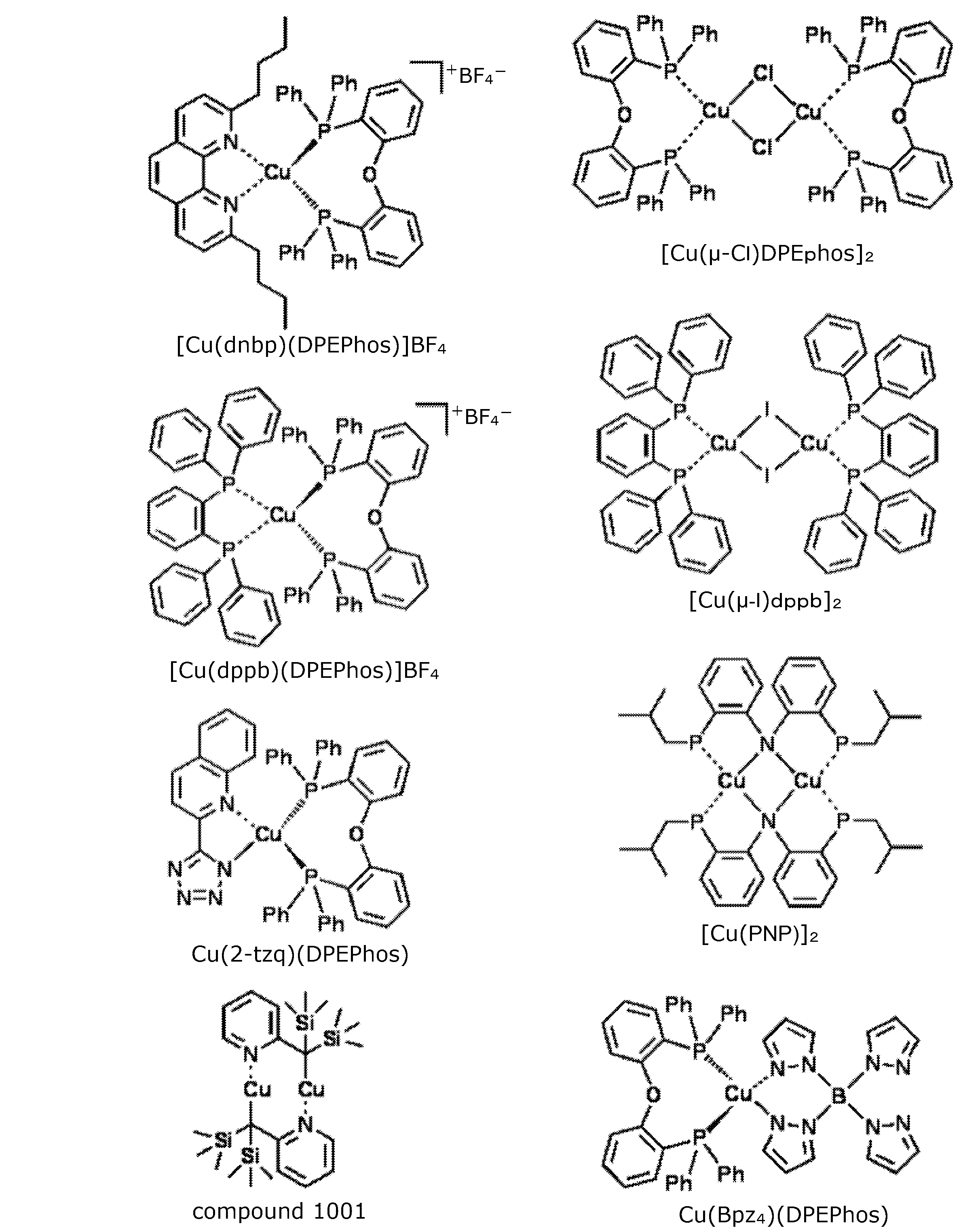
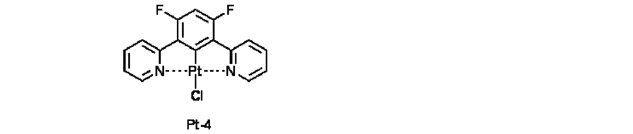
熱活性化型遅延蛍光材料としては、例えば下記のPIC-TRZ、[Cu(PNP-tBu)]2を好ましい例として挙げることができる。

エキサイプレックス型発光材料としては、例えば下記のm-MTDATAとPBD、PyPySPyPyとNPB、PPSPPとNPBを好ましい例として挙げることができる。

上に代表的な発光材料の具体例を記載したが、本発明に用いることができる発光材料はこれらに限定されるものではなく、その他の公知の発光材料も用いることができる。主な発光材料は、例えば、シーエムシー出版、「有機ELのデバイス物理・材料化学・デバイス応用」の第9章に記載されている。
(注入層)
注入層とは、駆動電圧低下や発光輝度向上のために電極と有機層間に設けられる層のことで、正孔注入層と電子注入層があり、陽極と発光層または正孔輸送層の間、および陰極と発光層または電子輸送層との間に存在させてもよい。注入層は必要に応じて設けることができる。
注入層とは、駆動電圧低下や発光輝度向上のために電極と有機層間に設けられる層のことで、正孔注入層と電子注入層があり、陽極と発光層または正孔輸送層の間、および陰極と発光層または電子輸送層との間に存在させてもよい。注入層は必要に応じて設けることができる。
(阻止層)
阻止層は、発光層中に存在する電荷(電子もしくは正孔)および/または励起子の発光層外への拡散を阻止することができる層である。電子阻止層は、発光層および正孔輸送層の間に配置されることができ、電子が正孔輸送層の方に向かって発光層を通過することを阻止する。同様に、正孔阻止層は発光層および電子輸送層の間に配置されることができ、正孔が電子輸送層の方に向かって発光層を通過することを阻止する。阻止層はまた、励起子が発光層の外側に拡散することを阻止するために用いることができる。すなわち電子阻止層、正孔阻止層はそれぞれ励起子阻止層としての機能も兼ね備えることができる。本明細書でいう電子阻止層または励起子阻止層は、一つの層で電子阻止層および励起子阻止層の機能を有する層を含む意味で使用される。
阻止層は、発光層中に存在する電荷(電子もしくは正孔)および/または励起子の発光層外への拡散を阻止することができる層である。電子阻止層は、発光層および正孔輸送層の間に配置されることができ、電子が正孔輸送層の方に向かって発光層を通過することを阻止する。同様に、正孔阻止層は発光層および電子輸送層の間に配置されることができ、正孔が電子輸送層の方に向かって発光層を通過することを阻止する。阻止層はまた、励起子が発光層の外側に拡散することを阻止するために用いることができる。すなわち電子阻止層、正孔阻止層はそれぞれ励起子阻止層としての機能も兼ね備えることができる。本明細書でいう電子阻止層または励起子阻止層は、一つの層で電子阻止層および励起子阻止層の機能を有する層を含む意味で使用される。
(正孔阻止層)
正孔阻止層とは広い意味では電子輸送層の機能を有する。正孔阻止層は電子を輸送しつつ、正孔が電子輸送層へ到達することを阻止する役割があり、これにより発光層中での電子と正孔の再結合確率を向上させることができる。正孔阻止層の材料としては、後述する電子輸送層の材料を必要に応じて用いることができる。
正孔阻止層とは広い意味では電子輸送層の機能を有する。正孔阻止層は電子を輸送しつつ、正孔が電子輸送層へ到達することを阻止する役割があり、これにより発光層中での電子と正孔の再結合確率を向上させることができる。正孔阻止層の材料としては、後述する電子輸送層の材料を必要に応じて用いることができる。
(電子阻止層)
電子阻止層とは、広い意味では正孔を輸送する機能を有する。電子阻止層は正孔を輸送しつつ、電子が正孔輸送層へ到達することを阻止する役割があり、これにより発光層中での電子と正孔が再結合する確率を向上させることができる。
電子阻止層とは、広い意味では正孔を輸送する機能を有する。電子阻止層は正孔を輸送しつつ、電子が正孔輸送層へ到達することを阻止する役割があり、これにより発光層中での電子と正孔が再結合する確率を向上させることができる。
(励起子阻止層)
励起子阻止層とは、発光層内で正孔と電子が再結合することにより生じた励起子が電荷輸送層に拡散することを阻止するための層であり、本層の挿入により励起子を効率的に発光層内に閉じ込めることが可能となり、素子の発光効率を向上させることができる。励起子阻止層は発光層に隣接して陽極側、陰極側のいずれにも挿入することができ、両方同時に挿入することも可能である。すなわち、励起子阻止層を陽極側に有する場合、正孔輸送層と発光層の間に、発光層に隣接して該層を挿入することができ、陰極側に挿入する場合、発光層と陰極との間に、発光層に隣接して該層を挿入することができる。また、陽極と、発光層の陽極側に隣接する励起子阻止層との間には、正孔注入層や電子阻止層などを有することができ、陰極と、発光層の陰極側に隣接する励起子阻止層との間には、電子注入層、電子輸送層、正孔阻止層などを有することができる。阻止層を配置する場合、阻止層として用いる材料の励起一重項エネルギーおよび励起三重項エネルギーの少なくともいずれか一方は、発光材料の励起一重項エネルギーおよび励起三重項エネルギーよりも高いことが好ましい。
励起子阻止層とは、発光層内で正孔と電子が再結合することにより生じた励起子が電荷輸送層に拡散することを阻止するための層であり、本層の挿入により励起子を効率的に発光層内に閉じ込めることが可能となり、素子の発光効率を向上させることができる。励起子阻止層は発光層に隣接して陽極側、陰極側のいずれにも挿入することができ、両方同時に挿入することも可能である。すなわち、励起子阻止層を陽極側に有する場合、正孔輸送層と発光層の間に、発光層に隣接して該層を挿入することができ、陰極側に挿入する場合、発光層と陰極との間に、発光層に隣接して該層を挿入することができる。また、陽極と、発光層の陽極側に隣接する励起子阻止層との間には、正孔注入層や電子阻止層などを有することができ、陰極と、発光層の陰極側に隣接する励起子阻止層との間には、電子注入層、電子輸送層、正孔阻止層などを有することができる。阻止層を配置する場合、阻止層として用いる材料の励起一重項エネルギーおよび励起三重項エネルギーの少なくともいずれか一方は、発光材料の励起一重項エネルギーおよび励起三重項エネルギーよりも高いことが好ましい。
(正孔輸送層)
正孔輸送層とは正孔を輸送する機能を有する正孔輸送材料からなり、正孔輸送層は単層または複数層設けることができる。
正孔輸送材料としては、正孔の注入または輸送、電子の障壁性のいずれかを有するものであり、有機物、無機物のいずれであってもよい。使用できる公知の正孔輸送材料としては例えば、トリアゾール誘導体、オキサジアゾール誘導体、イミダゾール誘導体、カルバゾール誘導体、インドロカルバゾール誘導体、ポリアリールアルカン誘導体、ピラゾリン誘導体およびピラゾロン誘導体、フェニレンジアミン誘導体、アリールアミン誘導体、アミノ置換カルコン誘導体、オキサゾール誘導体、スチリルアントラセン誘導体、フルオレノン誘導体、ヒドラゾン誘導体、スチルベン誘導体、シラザン誘導体、アニリン系共重合体、また導電性高分子オリゴマー、特にチオフェンオリゴマー等が挙げられるが、ポルフィリン化合物、芳香族第3級アミン化合物およびスチリルアミン化合物を用いることが好ましく、芳香族第3級アミン化合物を用いることがより好ましい。
正孔輸送層とは正孔を輸送する機能を有する正孔輸送材料からなり、正孔輸送層は単層または複数層設けることができる。
正孔輸送材料としては、正孔の注入または輸送、電子の障壁性のいずれかを有するものであり、有機物、無機物のいずれであってもよい。使用できる公知の正孔輸送材料としては例えば、トリアゾール誘導体、オキサジアゾール誘導体、イミダゾール誘導体、カルバゾール誘導体、インドロカルバゾール誘導体、ポリアリールアルカン誘導体、ピラゾリン誘導体およびピラゾロン誘導体、フェニレンジアミン誘導体、アリールアミン誘導体、アミノ置換カルコン誘導体、オキサゾール誘導体、スチリルアントラセン誘導体、フルオレノン誘導体、ヒドラゾン誘導体、スチルベン誘導体、シラザン誘導体、アニリン系共重合体、また導電性高分子オリゴマー、特にチオフェンオリゴマー等が挙げられるが、ポルフィリン化合物、芳香族第3級アミン化合物およびスチリルアミン化合物を用いることが好ましく、芳香族第3級アミン化合物を用いることがより好ましい。
(電子輸送層)
電子輸送層とは電子を輸送する機能を有する材料からなり、電子輸送層は単層または複数層設けることができる。
電子輸送材料(正孔阻止材料を兼ねる場合もある)としては、陰極より注入された電子を発光層に伝達する機能を有していればよい。使用できる電子輸送層としては例えば、ニトロ置換フルオレン誘導体、ジフェニルキノン誘導体、チオピランジオキシド誘導体、カルボジイミド、フレオレニリデンメタン誘導体、アントラキノジメタンおよびアントロン誘導体、オキサジアゾール誘導体等が挙げられる。さらに、上記オキサジアゾール誘導体において、オキサジアゾール環の酸素原子を硫黄原子に置換したチアジアゾール誘導体、電子吸引基として知られているキノキサリン環を有するキノキサリン誘導体も、電子輸送材料として用いることができる。さらにこれらの材料を高分子鎖に導入した、またはこれらの材料を高分子の主鎖とした高分子材料を用いることもできる。
電子輸送層とは電子を輸送する機能を有する材料からなり、電子輸送層は単層または複数層設けることができる。
電子輸送材料(正孔阻止材料を兼ねる場合もある)としては、陰極より注入された電子を発光層に伝達する機能を有していればよい。使用できる電子輸送層としては例えば、ニトロ置換フルオレン誘導体、ジフェニルキノン誘導体、チオピランジオキシド誘導体、カルボジイミド、フレオレニリデンメタン誘導体、アントラキノジメタンおよびアントロン誘導体、オキサジアゾール誘導体等が挙げられる。さらに、上記オキサジアゾール誘導体において、オキサジアゾール環の酸素原子を硫黄原子に置換したチアジアゾール誘導体、電子吸引基として知られているキノキサリン環を有するキノキサリン誘導体も、電子輸送材料として用いることができる。さらにこれらの材料を高分子鎖に導入した、またはこれらの材料を高分子の主鎖とした高分子材料を用いることもできる。
本発明の有機エレクトロルミネッセンス素子は、陽極と陰極の間に電界を印加することにより発光する。このとき、励起一重項エネルギーによる発光であれば、そのエネルギーレベルに応じた波長の光が、蛍光発光および遅延蛍光発光として確認される。また、励起三重項エネルギーによる発光であれば、そのエネルギーレベルに応じた波長が、りん光として確認される。通常の蛍光は、遅延蛍光発光よりも蛍光寿命が短いため、発光寿命は蛍光と遅延蛍光で区別できる。
一方、りん光については、本発明の化合物のような通常の有機化合物では、励起三重項エネルギーは不安定で熱等に変換され、寿命が短く直ちに失活するため、室温では殆ど観測できない。通常の有機化合物の励起三重項エネルギーを測定するためには、極低温の条件での発光を観測することにより測定可能である。
一方、りん光については、本発明の化合物のような通常の有機化合物では、励起三重項エネルギーは不安定で熱等に変換され、寿命が短く直ちに失活するため、室温では殆ど観測できない。通常の有機化合物の励起三重項エネルギーを測定するためには、極低温の条件での発光を観測することにより測定可能である。
[トランジスタ]
本発明のトランジスタは、バイポーラ型トランジスタであっても電界効果型トランジスタ(ユニポーラト型トランジスタ)であってもよい。本発明のトランジスタがnpn型バイポーラトランジスタである場合、エミッタ電極およびコレクタ電極の少なくとも一方が本発明の電極で構成されていること好ましく、エミッタ電極およびコレクタ電極の両方が本発明の電極で構成されていることがより好ましい。本発明のトランジスタがpnp型バイポーラトランジスタである場合、ベース電極が本発明の電極で構成されていることが好ましい。本発明のトランジスタが電界効果型トランジスタである場合、ソース電極およびドレイン電極の少なくとも一方が本発明の電極で構成されていることが好ましく、ソース電極およびドレイン電極の両方が本発明の電極で構成されていることが好ましい。また、電界効果型トランジスタの半導体層は、nチャネル型半導体層またはn型の有機半導体層であることが好ましい。以下に、代表として、電界効果型トランジスタの構成について説明する。
本発明のトランジスタは、バイポーラ型トランジスタであっても電界効果型トランジスタ(ユニポーラト型トランジスタ)であってもよい。本発明のトランジスタがnpn型バイポーラトランジスタである場合、エミッタ電極およびコレクタ電極の少なくとも一方が本発明の電極で構成されていること好ましく、エミッタ電極およびコレクタ電極の両方が本発明の電極で構成されていることがより好ましい。本発明のトランジスタがpnp型バイポーラトランジスタである場合、ベース電極が本発明の電極で構成されていることが好ましい。本発明のトランジスタが電界効果型トランジスタである場合、ソース電極およびドレイン電極の少なくとも一方が本発明の電極で構成されていることが好ましく、ソース電極およびドレイン電極の両方が本発明の電極で構成されていることが好ましい。また、電界効果型トランジスタの半導体層は、nチャネル型半導体層またはn型の有機半導体層であることが好ましい。以下に、代表として、電界効果型トランジスタの構成について説明する。
電界効果型トランジスタは、分離して設けられたソース電極およびドレイン電極と、ソース電極とドレイン電極の間に設けられた半導体層と、この半導体層と重なるように、ゲート絶縁層を介して設けられたゲート電極とを少なくとも有しており、ソース電極およびドレインの少なくとも一方が本発明の電極により構成されている。本発明の電極により構成されるのは、ソース電極のみ、または、ドレイン電極のみであってもよいし、ソース電極およびドレイン電極の両方であってもよいが、ソース電極およびドレイン電極の両方が本発明の電極により構成されていることが好ましい。この実施形態ではソース電極およびドレイン電極の両方が本発明の電極で構成されている場合を例にする。具体的な電界効果型トランジスタの構造例を図2に示す。図2において、11はソース電極、12はドレイン電極、13は半導体層、14はゲート絶縁層、15は基板を兼ねるゲート電極を表す。図2に示す電界効果型トランジスタは、ソース電極、ドレイン電極およびゲート電極が半導体層よりも基板側にあるボトムコンタクト・ボトムゲート型トランジスタとして構成されている。
以下において、電界効果型トランジスタの各部材および各層について説明する。
以下において、電界効果型トランジスタの各部材および各層について説明する。
(基板)
電界効果型トランジスタは、基板に支持されていることが好ましい。基板の具体例としては、上記の有機エレクトロルミネッセンス素子における基板の具体例と同様のものを挙げることができる。
電界効果型トランジスタは、基板に支持されていることが好ましい。基板の具体例としては、上記の有機エレクトロルミネッセンス素子における基板の具体例と同様のものを挙げることができる。
(ゲート電極)
ゲート電極の構成材料としては、導電性を示す材料であれば特に制限されず、公知の材料を任意に選択して用いることができる。ゲート電極の材料の例としては、白金、金、アルミニウム、クロム、ニッケル、銅、チタン、マグネシウム、カルシウム、バリウム、ナトリウム等の金属、InO2、SnO2、ITO等の導電性金属酸化物、樟脳スルホン酸がドープされたポリアニリン、パラトルエンスルホン酸がドープされたポリエチレンジオキシチオフェン等の、ドープされた導電性高分子、および、カーボンブラック、グラファイト粉、金属微粒子等がバインダーに分散されてなる導電性複合材料等が挙げられる。これらの材料は、いずれか一種を単独で用いてもよく、二種以上を任意の比率および組み合わせで併用してもよい。また、基板としてシリコン基板を用いる場合には、該シリコン基板にn型不純物をドープした領域をゲート電極として用いてもよい。n型不純物としては、リン(P)やヒ素(As)等の15族元素を挙げることができる。
ゲート電極の構成材料としては、導電性を示す材料であれば特に制限されず、公知の材料を任意に選択して用いることができる。ゲート電極の材料の例としては、白金、金、アルミニウム、クロム、ニッケル、銅、チタン、マグネシウム、カルシウム、バリウム、ナトリウム等の金属、InO2、SnO2、ITO等の導電性金属酸化物、樟脳スルホン酸がドープされたポリアニリン、パラトルエンスルホン酸がドープされたポリエチレンジオキシチオフェン等の、ドープされた導電性高分子、および、カーボンブラック、グラファイト粉、金属微粒子等がバインダーに分散されてなる導電性複合材料等が挙げられる。これらの材料は、いずれか一種を単独で用いてもよく、二種以上を任意の比率および組み合わせで併用してもよい。また、基板としてシリコン基板を用いる場合には、該シリコン基板にn型不純物をドープした領域をゲート電極として用いてもよい。n型不純物としては、リン(P)やヒ素(As)等の15族元素を挙げることができる。
ゲート電極の厚みは、特に制限されるものではないが、通常0.01μm以上、中でも0.02μm以上、また、通常2μm以下、中でも1μm以下の範囲とすることが好ましい。
(ゲート絶縁層)
ゲート絶縁層は、ゲート電極とソース電極およびドレイン電極とのオーバーラッピング領域、並びにゲート電極上のチャネル領域を電気的絶縁領域として維持する機能を有する層である。なお、ここで「電気的絶縁」とは、電気伝導度が10-9S/cm以下のことを言う。
ゲート絶縁層は、ゲート電極とソース電極およびドレイン電極とのオーバーラッピング領域、並びにゲート電極上のチャネル領域を電気的絶縁領域として維持する機能を有する層である。なお、ここで「電気的絶縁」とは、電気伝導度が10-9S/cm以下のことを言う。
ゲート絶縁層の材料は、絶縁性を有する材料ならば特に限定されないが、例えば、ポリメチル(メタ)アクリレート、ポリスチレン、ポリビニルフェノール、ポリイミド、ポリカーボネート、ポリエステル、ポリビニルアルコール、ポリ酢酸ビニル、ポリウレタン、ポリスルホン、ポリイミド樹脂、ポリアミド樹脂、エポキシ樹脂、フェノール樹脂等のポリマーおよびこれらを組み合わせた共重合体、二酸化珪素、酸化アルミニウム、酸化チタン等の酸化物、SrTiO3、BaTiO3等の強誘電性酸化物、窒化珪素等の窒化物、硫化物、フッ化物等の誘電体、或いはこれら誘電体の粒子を分散させたポリマー、等が挙げられる。これらの材料は、いずれか一種を単独で用いてもよく、二種以上を任意の比率および組み合わせで併用してもよい。また、基板としてシリコン基板を用いる場合には、該シリコン基板を熱酸化することで形成したSiO2層をゲート絶縁層として用いてもよい。
ゲート絶縁層としては、ゲート電極への漏れ電流、電界効果トランジスタの低ゲート電圧駆動に関係することから、室温での電気伝導度が通常10-9S/cm以下、中でも10-14S/cm以下であることが好ましい。また、比誘電率が通常2.0以上、中でも2.5以上であることが好ましい。
ゲート絶縁層の厚みは、通常0.01μm以上、中でも0.1μm以上、更には0.2μm以上、また、通常4μm以下、中でも2μm以下、更には1μm以下の範囲であることが好ましい。
(半導体層)
半導体層の構成材料は、有機半導体であっても無機半導体であってもよい。無機半導体としては酸化物半導体を用いることが好ましい。
有機半導体はn型有機半導体であることが好ましい。n型有機半導体の例として、フラーレン(C60、C70、C76)、オクタアザポルフィリン、p型有機半導体のパーフルオロ体、ナフタレンテトラカルボン酸無水物、ナフタレンテトラカルボン酸ジイミド、ペリレンテトラカルボン酸無水物、ペリレンテトラカルボン酸ジイミド等の芳香族カルボン酸無水物やそのイミド化物、および、これら化合物を骨格として含む誘導体等を挙げることができる。また、パーフルオロ体とするp型有機半導体の好ましい範囲と具体例については、後述の太陽電池で用いるp型有機半導体の好ましい範囲と具体例を参照することができる。
酸化物半導体としては、酸化亜鉛、酸化ニッケル、酸化スズ、酸化チタン、酸化バナジウム、酸化インジウム、チタン酸ストロンチウム、In-Ga-Zn-O系化合物等を挙げることができる。
半導体層の構成材料は、有機半導体であっても無機半導体であってもよい。無機半導体としては酸化物半導体を用いることが好ましい。
有機半導体はn型有機半導体であることが好ましい。n型有機半導体の例として、フラーレン(C60、C70、C76)、オクタアザポルフィリン、p型有機半導体のパーフルオロ体、ナフタレンテトラカルボン酸無水物、ナフタレンテトラカルボン酸ジイミド、ペリレンテトラカルボン酸無水物、ペリレンテトラカルボン酸ジイミド等の芳香族カルボン酸無水物やそのイミド化物、および、これら化合物を骨格として含む誘導体等を挙げることができる。また、パーフルオロ体とするp型有機半導体の好ましい範囲と具体例については、後述の太陽電池で用いるp型有機半導体の好ましい範囲と具体例を参照することができる。
酸化物半導体としては、酸化亜鉛、酸化ニッケル、酸化スズ、酸化チタン、酸化バナジウム、酸化インジウム、チタン酸ストロンチウム、In-Ga-Zn-O系化合物等を挙げることができる。
有機半導体層の膜厚は、薄過ぎると電流の流れる部分が制限され、特性が不充分になってしまう傾向があり、厚過ぎると成膜に必要な材料が多くなったり、成膜時間が長くなったりしてコストアップにつながり、且つ、オフ電流が流れやすくなりオンオフ比を大きく取れなくなる傾向がある。従って、好ましい有機半導体層の膜厚は、通常5nm以上、中でも10nm以上、更には30nm以上、また、通常10μm以下、中でも1μm以下、更には500nm以下の範囲である。
(ソース電極およびドレイン電極)
ソース電極およびドレイン電極は、本発明の電極により構成されている。本発明の電極は仕事関数が小さいため、ソース電極およびドレイン電極を本発明の電極で構成することにより、半導体層に効率よく電子を注入することができるとともに、ソース電極と半導体層、半導体層とドレイン電極の接触状態をオーミック接触にすることができる。これにより、駆動電圧が低くなり、また、良好な電圧電流特性を得ることができる。
トランジスタのソース電極およびドレイン電極に用いる電極の仕事関数は、これらの電極と接合している半導体層が有機半導体層である場合には、その有機半導体層のLUMO準位の絶対値をELUMOとしたとき、ELUMO±1.5eVであることが好ましく、ELUMO±1.0eVであることがより好ましく、ELUMO±0.5eVであることがさらに好ましい。
また、トランジスタのソース電極およびドレイン電極に用いる電極の仕事関数は、これらの電極と接合している半導体層が無機半導体層である場合には、無機半導体層の電子親和力、すなわち伝導帯の底から真空準位までのエネルギーをχとしたとき、χ±1.5eVであることが好ましく、χ±1.0eVであることがより好ましく、χ±0.5eVであることがさらに好ましい。
さらに、ソース電極およびドレイン電極に用いる電極の仕事関数は、これらの電極と接合している半導体層の仕事関数以下であることが特に好ましい。
ソース電極およびドレイン電極は、本発明の電極により構成されている。本発明の電極は仕事関数が小さいため、ソース電極およびドレイン電極を本発明の電極で構成することにより、半導体層に効率よく電子を注入することができるとともに、ソース電極と半導体層、半導体層とドレイン電極の接触状態をオーミック接触にすることができる。これにより、駆動電圧が低くなり、また、良好な電圧電流特性を得ることができる。
トランジスタのソース電極およびドレイン電極に用いる電極の仕事関数は、これらの電極と接合している半導体層が有機半導体層である場合には、その有機半導体層のLUMO準位の絶対値をELUMOとしたとき、ELUMO±1.5eVであることが好ましく、ELUMO±1.0eVであることがより好ましく、ELUMO±0.5eVであることがさらに好ましい。
また、トランジスタのソース電極およびドレイン電極に用いる電極の仕事関数は、これらの電極と接合している半導体層が無機半導体層である場合には、無機半導体層の電子親和力、すなわち伝導帯の底から真空準位までのエネルギーをχとしたとき、χ±1.5eVであることが好ましく、χ±1.0eVであることがより好ましく、χ±0.5eVであることがさらに好ましい。
さらに、ソース電極およびドレイン電極に用いる電極の仕事関数は、これらの電極と接合している半導体層の仕事関数以下であることが特に好ましい。
ソース電極およびドレイン電極の厚みは、特に制限されるものではないが、通常0.01μm以上、中でも0.02μm以上、また、通常2μm以下、中でも1μm以下の範囲とすることが好ましい。
(チャネル)
有機電界型トランジスタは、ソース電極およびドレイン電極で挟まれるチャネル部分の電流をゲート電極により制御して、スイッチング或いは増幅の動作をする。このチャネル部分の長さ(ソース電極とドレイン電極とのギャップ間隔)は、一般に狭いほどトランジスタとしての特性が上昇するが、狭過ぎるとオフ電流が増加したり、オンオフ比が小さくなったりする、いわゆるショートチャンネル効果が生じる傾向がある。また、チャネルの幅(ソース電極とドレイン電極との間の幅)が大きくなると、大きな電流を流せるようになるという点で好ましいが、大き過ぎると素子の面積が大きくなり、集積化の面で不利になる場合がある。なお、ソース電極およびドレイン電極を櫛型電極にすることにより、長いチャネル長を得ることができる。
有機電界型トランジスタは、ソース電極およびドレイン電極で挟まれるチャネル部分の電流をゲート電極により制御して、スイッチング或いは増幅の動作をする。このチャネル部分の長さ(ソース電極とドレイン電極とのギャップ間隔)は、一般に狭いほどトランジスタとしての特性が上昇するが、狭過ぎるとオフ電流が増加したり、オンオフ比が小さくなったりする、いわゆるショートチャンネル効果が生じる傾向がある。また、チャネルの幅(ソース電極とドレイン電極との間の幅)が大きくなると、大きな電流を流せるようになるという点で好ましいが、大き過ぎると素子の面積が大きくなり、集積化の面で不利になる場合がある。なお、ソース電極およびドレイン電極を櫛型電極にすることにより、長いチャネル長を得ることができる。
従って、チャネル長は、通常100nm以上、中でも500nm以上、更には1μm以上、また、通常1mm以下、中でも100μm以下、更には50μm以下の範囲であることが好ましい。また、チャネルの幅は、通常500nm以上、中でも5μm以上、更には10μm以上、また、通常20mm以下、中でも5mm以下、更には1mm以下の範囲であることが好ましい。
[太陽電池]
本発明の太陽電池は、少なくとも陽極、陰極、および陽極と陰極の間に発電層を形成した構造を有しており、陰極が本発明の電極により構成されていることが好ましい。発電層は、少なくとも光電変換層を含むものであり、光電変換層のみからなるものであってもよいし、光電変換層の他に1層以上の機能層を有するものであってもよい。そのような他の機能層として、正孔取出し層、正孔輸送層、電子阻止層、正孔阻止層、電子輸送層、電子取出し層などを挙げることができる。具体的な太陽電池の構造例を図3に示す。図3において、21は基板、22は陰極、23は電子取出し層、24は光電変換層、25は正孔取出し層、26は陽極を表わす。
以下において、太陽電池を構成する各部材および各層について説明する。
本発明の太陽電池は、少なくとも陽極、陰極、および陽極と陰極の間に発電層を形成した構造を有しており、陰極が本発明の電極により構成されていることが好ましい。発電層は、少なくとも光電変換層を含むものであり、光電変換層のみからなるものであってもよいし、光電変換層の他に1層以上の機能層を有するものであってもよい。そのような他の機能層として、正孔取出し層、正孔輸送層、電子阻止層、正孔阻止層、電子輸送層、電子取出し層などを挙げることができる。具体的な太陽電池の構造例を図3に示す。図3において、21は基板、22は陰極、23は電子取出し層、24は光電変換層、25は正孔取出し層、26は陽極を表わす。
以下において、太陽電池を構成する各部材および各層について説明する。
(基板)
本発明の太陽電池は、基板に支持されていることが好ましい。基板の具体例については、有機エレクトロルミネッセンス素子における基板の具体例と同様のものを挙げることができる。この他に、金属箔や、金属箔と樹脂フィルムの積層体も基板として用いることができる。
本発明の太陽電池は、基板に支持されていることが好ましい。基板の具体例については、有機エレクトロルミネッセンス素子における基板の具体例と同様のものを挙げることができる。この他に、金属箔や、金属箔と樹脂フィルムの積層体も基板として用いることができる。
(陰極)
陰極は、発電層からの電子を取り出す機能を有する。
陰極は、本発明の電極により構成されている。本発明の電極は仕事関数が小さいため、陰極を本発明の電極で構成することにより、陰極の仕事関数と陽極の仕事関数の差が大きくなり、高い開放電圧を得ることができる。また、陰極と半導体層(図3に示す太陽電池では電子取出し層23)の接触状態をオーミック接触にすることができるため、半導体層からの電子を陰極へ効率よく取り出すことができる。これにより、高いエネルギー変換効率を得ることができる。
太陽電池の陰極に用いる電極の仕事関数は、その陰極と接合している半導体層が有機半導体層である場合には、その有機半導体層のLUMO準位の絶対値をELUMOとしたとき、ELUMO±1.5eVであることが好ましく、ELUMO±1.0eVであることがより好ましく、ELUMO±0.5eVであることがさらに好ましい。
また、太陽電池の陰極に用いる電極の仕事関数は、その陰極と接合している半導体層が無機半導体層である場合には、無機半導体層の電子親和力、すなわち伝導帯の底から真空準位までのエネルギーをχとしたとき、χ±1.5eVであることが好ましく、χ±1.0eVであることがより好ましく、χ±0.5eVであることがさらに好ましい。
さらに、太陽電池の陰極に用いる電極の仕事関数は、その陰極と接合している半導体層の仕事関数以下であることが好ましい。
陰極は、発電層からの電子を取り出す機能を有する。
陰極は、本発明の電極により構成されている。本発明の電極は仕事関数が小さいため、陰極を本発明の電極で構成することにより、陰極の仕事関数と陽極の仕事関数の差が大きくなり、高い開放電圧を得ることができる。また、陰極と半導体層(図3に示す太陽電池では電子取出し層23)の接触状態をオーミック接触にすることができるため、半導体層からの電子を陰極へ効率よく取り出すことができる。これにより、高いエネルギー変換効率を得ることができる。
太陽電池の陰極に用いる電極の仕事関数は、その陰極と接合している半導体層が有機半導体層である場合には、その有機半導体層のLUMO準位の絶対値をELUMOとしたとき、ELUMO±1.5eVであることが好ましく、ELUMO±1.0eVであることがより好ましく、ELUMO±0.5eVであることがさらに好ましい。
また、太陽電池の陰極に用いる電極の仕事関数は、その陰極と接合している半導体層が無機半導体層である場合には、無機半導体層の電子親和力、すなわち伝導帯の底から真空準位までのエネルギーをχとしたとき、χ±1.5eVであることが好ましく、χ±1.0eVであることがより好ましく、χ±0.5eVであることがさらに好ましい。
さらに、太陽電池の陰極に用いる電極の仕事関数は、その陰極と接合している半導体層の仕事関数以下であることが好ましい。
(陽極)
陽極は、発電層からの正孔を取り出す機能を有する。
陽極には、仕事関数の大きい導電性透明材料を用いることが好ましい。陽極に用いる導電性材料の具体例としては、有機エレクトロルミネッセンス素子における陽極の具体例と同様のものを挙げることができる。
陽極は、発電層からの正孔を取り出す機能を有する。
陽極には、仕事関数の大きい導電性透明材料を用いることが好ましい。陽極に用いる導電性材料の具体例としては、有機エレクトロルミネッセンス素子における陽極の具体例と同様のものを挙げることができる。
(光電変換層)
光電変換層は、光エネルギーを電気エネルギーに変換する層である。
光電変換層に用いられる材料としては、薄膜単結晶シリコン、薄膜多結晶シリコン、アモルファスシリコン、微結晶シリコン、球状シリコン、無機半導体、有機色素、有機半導体を挙げることができる。また、光電変換層は、スタック型、積層型、タンデム型のような多接合型になっていてもよい。
無機半導体(化合物半導体)は、S、Se、Teなどのカルコゲン元素を含むカルコゲナイド系半導体であることが好ましく、I-III-VI2族半導体(カルコパイライト系)であることがより好ましく、I族元素としてCuを用いたCu-III-VI2族半導体であることがさらに好ましく、CIS系半導体〔CuIn(Se1-ySy)2;0≦y≦1〕やCIGS系半導体〔Cu(In1-xGax)(Se1-ySy)2;0<x<1、0≦y≦1〕〕であることが特に好ましい。
光電変換層は、光エネルギーを電気エネルギーに変換する層である。
光電変換層に用いられる材料としては、薄膜単結晶シリコン、薄膜多結晶シリコン、アモルファスシリコン、微結晶シリコン、球状シリコン、無機半導体、有機色素、有機半導体を挙げることができる。また、光電変換層は、スタック型、積層型、タンデム型のような多接合型になっていてもよい。
無機半導体(化合物半導体)は、S、Se、Teなどのカルコゲン元素を含むカルコゲナイド系半導体であることが好ましく、I-III-VI2族半導体(カルコパイライト系)であることがより好ましく、I族元素としてCuを用いたCu-III-VI2族半導体であることがさらに好ましく、CIS系半導体〔CuIn(Se1-ySy)2;0≦y≦1〕やCIGS系半導体〔Cu(In1-xGax)(Se1-ySy)2;0<x<1、0≦y≦1〕〕であることが特に好ましい。
光電変換層を有機半導体で構成する場合、p型有機半導体とn型有機半導体が層内で相分離した層(i層)を有するバルクヘテロ接合型、p型有機半導体を含む層(p層)とn型有機半導体を含む層(n層)を積層した積層型(ヘテロpn接合型)、PIN型、ショットキー型や、これらを組み合わせた構成とすることが好ましく、中でも、バルクヘテロ接合型とすることがより好ましい。
p型有機半導体として、π共役高分子材料やπ共役低分子有機化合物などを好ましく用いることができる。共役高分子材料は、単一あるいは複数種のπ共役モノマーを重合したものである。π共役モノマーとしては、チオフェン、フルオレン、カルバゾール、ジフェニルチオフェン、ジチエノチオフェン、ジチエノシロール、ジチエノシクロヘキサン、ベンゾチアジアゾール、チエノチオフェン、イミドチオフェン、ベンゾジチオフェン、およおび、これらの化合物を骨格として含む誘導体等を挙げることができる。これらのモノマーは直接結合していてもよいし、CH=CHやC三C、NやOを介して結合していてもよい。低分子有機半導体材料としてはペンタセンやナフタセン等の縮合芳香族炭化水素、チオフェン環を4個以上結合したオリゴチオフェン類、ポルフィリン化合物やテトラベンゾポルフィリン化合物及びその金属錯体、並びにフタロシアニン化合物及びその金属錯体等が挙げられる。
n型半導体化合物としては、フラーレン(C60、C70、C76)、オクタアザポルフィリン、上記のp型有機半導体のパーフルオロ体、ナフタレンテトラカルボン酸無水物、ナフタレンテトラカルボン酸ジイミド、ペリレンテトラカルボン酸無水物、ペリレンテトラカルボン酸ジイミド等の芳香族カルボン酸無水物やそのイミド化物、および、これら化合物を骨格として含む誘導体等を挙げることができる。
(電子取出層)
電子取出層は陰極への電子注入を容易にする層である。
電子取出層の材料としては、LiF等のアルカリ金属塩、酸化チタン(TiOx)、酸化亜鉛(ZnO)のようなn型酸化物半導体等を挙げることができる。その他に、バソキュプロイン(BCP)、バソフェナントレン(Bphen)等のフェナントレン誘導体、P=OあるいはP=S構造を有するホスフィン化合物も電子取出層の材料に用いることができ、中でも、リン原子に芳香族炭化水素基又は芳香族複素環基が結合したホスフィン化合物を用いることが好ましい。
電子取出層は陰極への電子注入を容易にする層である。
電子取出層の材料としては、LiF等のアルカリ金属塩、酸化チタン(TiOx)、酸化亜鉛(ZnO)のようなn型酸化物半導体等を挙げることができる。その他に、バソキュプロイン(BCP)、バソフェナントレン(Bphen)等のフェナントレン誘導体、P=OあるいはP=S構造を有するホスフィン化合物も電子取出層の材料に用いることができ、中でも、リン原子に芳香族炭化水素基又は芳香族複素環基が結合したホスフィン化合物を用いることが好ましい。
(正孔取出層)
正孔取出層は陽極への正孔注入を容易にする層である。
正孔取出層の材料としては、ポリチオフェン、ポリピロールまたはポリアニリン等に、スルホン酸やハロゲン等をドーピングした導電性ポリマーや、酸化モリブデンや酸化ニッケル等の仕事関数の大きな金属酸化物を用いることができる。
正孔取出層は陽極への正孔注入を容易にする層である。
正孔取出層の材料としては、ポリチオフェン、ポリピロールまたはポリアニリン等に、スルホン酸やハロゲン等をドーピングした導電性ポリマーや、酸化モリブデンや酸化ニッケル等の仕事関数の大きな金属酸化物を用いることができる。
この太陽電池では、太陽光等の光が照射されると、光電変換層を構成する材料が励起されて電荷が発生する。電荷のうち正孔は正極側に輸送されて陽極に取り出され、電子は陰極側に輸送されて陰極に取り出され、陽極と陰極の間に起電力が生じる。起電力が生じた陽極と陰極の間を導体で接続することにより、陽極から陰極に流れる電流を得ることができる。
本発明の素子を構成する各層および各部材の形成方法は特に限定されず、ドライプロセス、ウェットプロセスのどちらを用いてもよい。また、各層および各部材をパターニングする場合、リソグラフィー法を用いることができる。リソグラフィー法の説明、具体的な方法および工程については、本発明の構造体の製造方法におけるリソグラフィー法について説明、具体的な方法および工程を参照することができる。
以下に実施例を挙げて本発明の特徴をさらに具体的に説明する。以下に示す材料、処理内容、処理手順等は、本発明の趣旨を逸脱しない限り適宜変更することができる。したがって、本発明の範囲は以下に示す具体例により限定的に解釈されるべきものではない。
なお、反射率の測定は1280型卓上薄膜解析装置(n&k社)を用いて行い、仕事関数の測定は理研計器社製光電子分光装置(AC-2)を用いて行った。トランジスタの出力特性の測定は、半導体パラメーターアナライザー(アジレントテクノロジー社製:HP4155)を用い、酸素濃度および水分濃度が1ppm以下の不活性雰囲気下で行った。有機エレクトロルミネッセンス素子の発光面積の測定は有機EL信頼性評価装置評価測定装置EAS-26B(システム技研)を用いて行った。また、真空蒸着法による合金層の成膜は、1×10⁻⁴Pa以下の真空度で、構成元素毎に別々の蒸着源を用いる共蒸着法により行った。
なお、反射率の測定は1280型卓上薄膜解析装置(n&k社)を用いて行い、仕事関数の測定は理研計器社製光電子分光装置(AC-2)を用いて行った。トランジスタの出力特性の測定は、半導体パラメーターアナライザー(アジレントテクノロジー社製:HP4155)を用い、酸素濃度および水分濃度が1ppm以下の不活性雰囲気下で行った。有機エレクトロルミネッセンス素子の発光面積の測定は有機EL信頼性評価装置評価測定装置EAS-26B(システム技研)を用いて行った。また、真空蒸着法による合金層の成膜は、1×10⁻⁴Pa以下の真空度で、構成元素毎に別々の蒸着源を用いる共蒸着法により行った。
(実施例1) MgCa合金からなる電極の作製と評価
ガラス基板上に、真空蒸着法にて、膜厚50nmのMgCa膜を形成して電極とした。このとき、Caの濃度は、6原子%または25原子%として2種類のMgCa層を形成した。
また、比較として、ガラス基板上に、真空蒸着法にて、Al層、MgAu層、Mg層をそれぞれ50nmの膜厚で形成した。このとき、MgAu層のAuの濃度は10原子%とした。
作製した各層の反射率スペクトルを図4に示す。図4中、「Mg94Ca6」は6原子%のCaを含むMgCa層を表し、「Mg75Ca25」は25原子%のCaを含むMgCa層を表す。
図4に示すように、MgCa層は、Ca濃度が低い場合および高い場合のいずれにおいても、可視領域において高い反射率を有していた。
ガラス基板上に、真空蒸着法にて、膜厚50nmのMgCa膜を形成して電極とした。このとき、Caの濃度は、6原子%または25原子%として2種類のMgCa層を形成した。
また、比較として、ガラス基板上に、真空蒸着法にて、Al層、MgAu層、Mg層をそれぞれ50nmの膜厚で形成した。このとき、MgAu層のAuの濃度は10原子%とした。
作製した各層の反射率スペクトルを図4に示す。図4中、「Mg94Ca6」は6原子%のCaを含むMgCa層を表し、「Mg75Ca25」は25原子%のCaを含むMgCa層を表す。
図4に示すように、MgCa層は、Ca濃度が低い場合および高い場合のいずれにおいても、可視領域において高い反射率を有していた。
(実施例2) MgCa合金からなる構造体の作製と評価
以下のようにして、酸化膜付きシリコン基板上に、フォトリソグラフィー法にて、櫛型パターンのMgCa層を作製し、構造体とした。
まず、酸化膜付きシリコン基板を洗浄した後、ヘキサメチルジシラザン(HMDS)により表面処理を行った。次に、この基板上に、リフトオフ層形成用液(ローム アンド ハース社製:LOL1000)をスピンコート法により塗布した後、150℃でベーク処理を行い、その上に、ポジ型レジスト(東京応化工業社製:TMSR-8900)をスピンコート法により塗布し、110℃でベーク処理を行った。次に、ポジ型レジストに、目的のパターン(櫛型パターン)に対する反転パターンの石英フォトマスクを通して露光を行い、露光部分を現像液 (東京応化工業社製:NMD-3)で除去することにより、反転パターンにパターニングされたレジスト膜を得た。続いて、ガラスまたは酸化膜付きシリコンまたは石英基板の上に、真空蒸着法にて、レジストマスクを覆うようにMgCa合金を成膜し、膜厚50nmのMgCa層を形成した。このとき、MgCa合金におけるCaの濃度は10原子%とした。その後、N-メチルピロリドンを用いてレジスト膜と該レジスト膜直上のMgCa層を剥離して除去した。以上の工程により、櫛型パターンのMgCa層(構造体)を作製した。
作製したMgCa層の断面を観察したところ、各櫛の歯(凸部)の角が比較的シャープで安定していた。このことから、MgCa層は、リソグラフィー適性が非常に高いことを確認することができた。
また、作製した櫛型パターンのMgCa層について、光電子分光装置により紫外線を照射して光電子収率を測定した。紫外線の照射光エネルギーを横軸に、光電子収率の0.5乗(平方根)を縦軸にとったグラフを図5に示す。図5中、「0h」、「6h」、「24h」はプロセス完了後から電子収率測定までの試料保管(大気雰囲気)時間を表す。図5から、この櫛型パターンのMgCa層の仕事関数は3.6eVであり、極めて小さい値であった。
以下のようにして、酸化膜付きシリコン基板上に、フォトリソグラフィー法にて、櫛型パターンのMgCa層を作製し、構造体とした。
まず、酸化膜付きシリコン基板を洗浄した後、ヘキサメチルジシラザン(HMDS)により表面処理を行った。次に、この基板上に、リフトオフ層形成用液(ローム アンド ハース社製:LOL1000)をスピンコート法により塗布した後、150℃でベーク処理を行い、その上に、ポジ型レジスト(東京応化工業社製:TMSR-8900)をスピンコート法により塗布し、110℃でベーク処理を行った。次に、ポジ型レジストに、目的のパターン(櫛型パターン)に対する反転パターンの石英フォトマスクを通して露光を行い、露光部分を現像液 (東京応化工業社製:NMD-3)で除去することにより、反転パターンにパターニングされたレジスト膜を得た。続いて、ガラスまたは酸化膜付きシリコンまたは石英基板の上に、真空蒸着法にて、レジストマスクを覆うようにMgCa合金を成膜し、膜厚50nmのMgCa層を形成した。このとき、MgCa合金におけるCaの濃度は10原子%とした。その後、N-メチルピロリドンを用いてレジスト膜と該レジスト膜直上のMgCa層を剥離して除去した。以上の工程により、櫛型パターンのMgCa層(構造体)を作製した。
作製したMgCa層の断面を観察したところ、各櫛の歯(凸部)の角が比較的シャープで安定していた。このことから、MgCa層は、リソグラフィー適性が非常に高いことを確認することができた。
また、作製した櫛型パターンのMgCa層について、光電子分光装置により紫外線を照射して光電子収率を測定した。紫外線の照射光エネルギーを横軸に、光電子収率の0.5乗(平方根)を縦軸にとったグラフを図5に示す。図5中、「0h」、「6h」、「24h」はプロセス完了後から電子収率測定までの試料保管(大気雰囲気)時間を表す。図5から、この櫛型パターンのMgCa層の仕事関数は3.6eVであり、極めて小さい値であった。
(実施例3) MgCa合金をソース電極およびドレイン電極に用いた有機トランジスタの作製と評価
絶縁層として熱酸化膜(SiO2)が300nmの膜厚で形成されたヘビードープ型n+-Siウェハ(以下、「n+-Si基板」という)を用意した。ここでは、このn+-Si基板を基板として用いるとともに、そのn+領域をゲート電極とし、熱酸化膜をゲート絶縁層として使用した。
次に、このn+-Si基板の上に、実施例2と同様の手順で櫛型パターンのMgCa層を形成した。ただし、ここでは、MgCa合金におけるCaの濃度を10原子%とし、レジスト膜と該レジスト膜直上のMgCa層の剥離を、リムーバ液(ローム アンド ハース社製:Micro positremover 116)とアセトンを用いて行った。形成したMgCa層は、櫛の歯が、それぞれ交互にソース電極およびドレイン電極に対応しており、合計で20対の電極対を有するものである。ソース電極とドレイン電極の間隔は25μm、チャネル幅は4mmであった。
次に、n+-Si基板上に、真空蒸着法にて、ソース電極およびドレイン電極を覆うようにC60(n型半導体)を成膜し、膜厚50nmのC60層を形成した。このとき、蒸着速度は0.01nm/sであった。
以上の工程により、ボトムゲート・ボトムコンタクト型のトランジスタを作製した。
作製したトランジスタのドレイン電圧-ドレイン電流特性を図6左に示す。
図6左を見ると、ドレイン電圧-ドレイン電流曲線が原点を通って一次関数的に増大していることがわかる。このことから、このトランジスタでは、ソース電極-C60層-ドレイン電極からなる電流路がV=IR(V:ドレイン電圧、I:ドレイン電流、R:抵抗)を満たしており、各電極とC60層とがオーミック接触していることを確認することができた。
絶縁層として熱酸化膜(SiO2)が300nmの膜厚で形成されたヘビードープ型n+-Siウェハ(以下、「n+-Si基板」という)を用意した。ここでは、このn+-Si基板を基板として用いるとともに、そのn+領域をゲート電極とし、熱酸化膜をゲート絶縁層として使用した。
次に、このn+-Si基板の上に、実施例2と同様の手順で櫛型パターンのMgCa層を形成した。ただし、ここでは、MgCa合金におけるCaの濃度を10原子%とし、レジスト膜と該レジスト膜直上のMgCa層の剥離を、リムーバ液(ローム アンド ハース社製:Micro positremover 116)とアセトンを用いて行った。形成したMgCa層は、櫛の歯が、それぞれ交互にソース電極およびドレイン電極に対応しており、合計で20対の電極対を有するものである。ソース電極とドレイン電極の間隔は25μm、チャネル幅は4mmであった。
次に、n+-Si基板上に、真空蒸着法にて、ソース電極およびドレイン電極を覆うようにC60(n型半導体)を成膜し、膜厚50nmのC60層を形成した。このとき、蒸着速度は0.01nm/sであった。
以上の工程により、ボトムゲート・ボトムコンタクト型のトランジスタを作製した。
作製したトランジスタのドレイン電圧-ドレイン電流特性を図6左に示す。
図6左を見ると、ドレイン電圧-ドレイン電流曲線が原点を通って一次関数的に増大していることがわかる。このことから、このトランジスタでは、ソース電極-C60層-ドレイン電極からなる電流路がV=IR(V:ドレイン電圧、I:ドレイン電流、R:抵抗)を満たしており、各電極とC60層とがオーミック接触していることを確認することができた。
(比較例1) Auをソース電極およびドレイン電極に用いた有機トランジスタの作製と評価
MgCa合金の代わりにAuを用いてソース電極およびドレイン電極を形成したこと以外は、実施例3と同様にしてトランジスタを作製した。
作製したトランジスタのドレイン電圧-ドレイン電流特性を図6右に示す。
図6右を見ると、この測定電圧範囲ではドレイン電流は観測できず、図6に示すような良好な出力特性は得られなかった。これは、ソース電極およびドレイン電極とC60層との間のエネルギー障壁が大きく、ショットキー接触になっているためであると考えられる。
MgCa合金の代わりにAuを用いてソース電極およびドレイン電極を形成したこと以外は、実施例3と同様にしてトランジスタを作製した。
作製したトランジスタのドレイン電圧-ドレイン電流特性を図6右に示す。
図6右を見ると、この測定電圧範囲ではドレイン電流は観測できず、図6に示すような良好な出力特性は得られなかった。これは、ソース電極およびドレイン電極とC60層との間のエネルギー障壁が大きく、ショットキー接触になっているためであると考えられる。
(実施例4) MgCa合金を陰極に用いた有機エレクトロルミネッセンス素子の作製と評価
膜厚100nmのインジウム・スズ酸化物(ITO)からなる陽極が形成されたガラス基板上に、各薄膜を真空蒸着法にて、真空度1×10⁻⁴Paで積層した。具体的には、まず、ITO上にHATCNを10nmの厚さに形成し、その上にTrisPCzを30nmの厚さに形成した。次に、mCBPと4CzIPNを異なる蒸着源から共蒸着し、30nmの厚さの層を形成して発光層とした。この時、4CzIPNの濃度は15重量%とした。次に、T2Tを10nmの厚さに形成し、その上にBPyTP2を55nmの厚さに形成した。次に、陰極の平面形状に対応するパターンの石英フォトマスクを用いること以外は、実施例3のソース電極およびドレイン電極の形成工程と同様にして陰極を形成し、有機エレクトロルミネッセンス素子とした。このとき、MgCa合金におけるCaの濃度は30原子%とした。
膜厚100nmのインジウム・スズ酸化物(ITO)からなる陽極が形成されたガラス基板上に、各薄膜を真空蒸着法にて、真空度1×10⁻⁴Paで積層した。具体的には、まず、ITO上にHATCNを10nmの厚さに形成し、その上にTrisPCzを30nmの厚さに形成した。次に、mCBPと4CzIPNを異なる蒸着源から共蒸着し、30nmの厚さの層を形成して発光層とした。この時、4CzIPNの濃度は15重量%とした。次に、T2Tを10nmの厚さに形成し、その上にBPyTP2を55nmの厚さに形成した。次に、陰極の平面形状に対応するパターンの石英フォトマスクを用いること以外は、実施例3のソース電極およびドレイン電極の形成工程と同様にして陰極を形成し、有機エレクトロルミネッセンス素子とした。このとき、MgCa合金におけるCaの濃度は30原子%とした。
(比較例2) AlまたはMgAu合金を陰極に用いた有機エレクトロルミネッセンス素子の作製と評価
陰極を形成する際、MgCa合金の代わりにAlまたはMgAu合金を用いたこと以外は、実施例4と同様にして、陰極の材料が異なる2種類の有機エレクトロルミネッセンス素子を作製した。
実施例4および比較例2で作製した有機エレクトロルミネッセンス素子を室温25℃、相対湿度50%の条件下で放置し、その発光領域の大きさの経時変化を調べた。その結果を図7に示す。
図7に示すように、MgCa合金で陰極を形成した有機エレクトロルミネッセンス素子は、時間が経過しても発光面積が殆ど変わらず、200時間経過後においても広い発光面積を保持していた。このことから、MgCa合金からなる電極はバリア性にも優れていることを確認することができた。
陰極を形成する際、MgCa合金の代わりにAlまたはMgAu合金を用いたこと以外は、実施例4と同様にして、陰極の材料が異なる2種類の有機エレクトロルミネッセンス素子を作製した。
実施例4および比較例2で作製した有機エレクトロルミネッセンス素子を室温25℃、相対湿度50%の条件下で放置し、その発光領域の大きさの経時変化を調べた。その結果を図7に示す。
図7に示すように、MgCa合金で陰極を形成した有機エレクトロルミネッセンス素子は、時間が経過しても発光面積が殆ど変わらず、200時間経過後においても広い発光面積を保持していた。このことから、MgCa合金からなる電極はバリア性にも優れていることを確認することができた。
(実施例5) MgCa合金、MgCaAg合金またはMgCaAl合金からなる電極の作製と評価
真空蒸着法にて、MgCa層、MgCaAg層またはMgCaAl層を、それぞれガラス基板の上に膜厚100nmで形成して電極とした。
また、比較として、ガラス基板の上に、真空蒸着法にて、Al層を膜厚100nmで形成して電極とした。
作製した各層の組成比と仕事関数を表1に示す。また、作製した各層の反射率スペクトルを図8に示す。図8中に示した合金の組成は、表1に示した合金の組成に対応し、数値は原子%での組成比を表す。また、以下の説明における合金の組成についても同様である。
真空蒸着法にて、MgCa層、MgCaAg層またはMgCaAl層を、それぞれガラス基板の上に膜厚100nmで形成して電極とした。
また、比較として、ガラス基板の上に、真空蒸着法にて、Al層を膜厚100nmで形成して電極とした。
作製した各層の組成比と仕事関数を表1に示す。また、作製した各層の反射率スペクトルを図8に示す。図8中に示した合金の組成は、表1に示した合金の組成に対応し、数値は原子%での組成比を表す。また、以下の説明における合金の組成についても同様である。
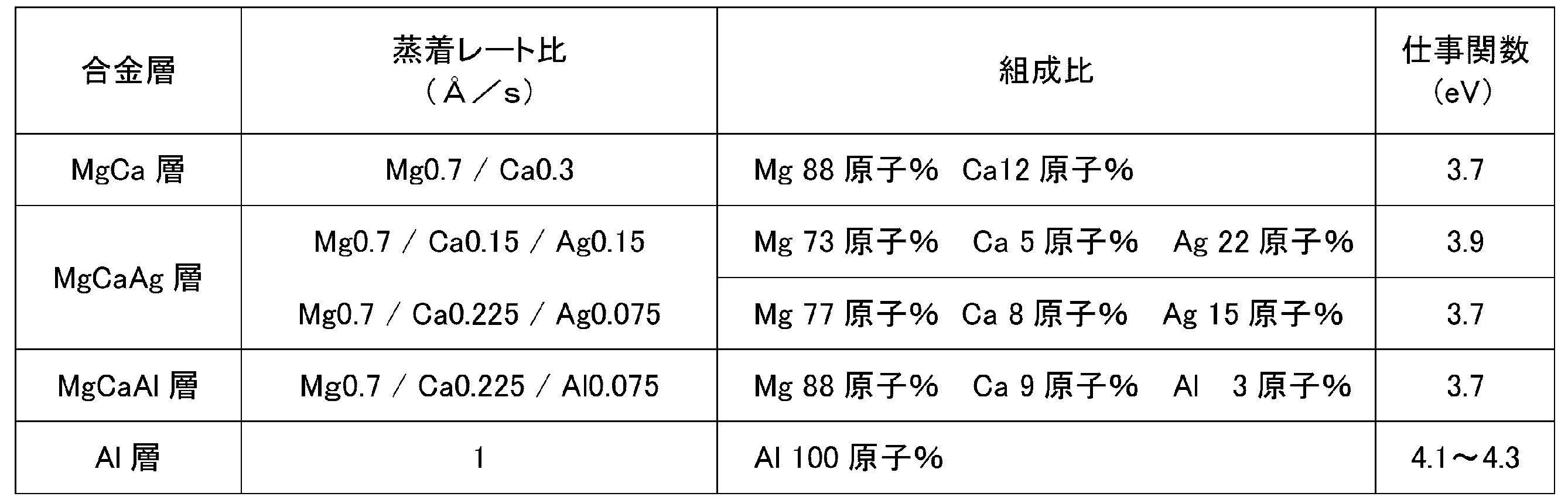
表1に示しているように、MgCaAg合金、MgCaAl合金の仕事関数は、MgCa合金と同様に極めて小さい値であった。
また、図8から、MgCa層、MgCaAg層、MgCaAl層は、いずれも可視光領域で高い反射率を示すが、特に、MgCaAg層、MgCaAl層は、450nm以下の短波長領域で、MgCa層よりも高い80%以上の反射率を示すことがわかる。このことから、AgやAlを第3成分として合金に添加することにより、可視光領域全般で80%以上の高い反射率を達成できることがわかった。
また、図8から、MgCa層、MgCaAg層、MgCaAl層は、いずれも可視光領域で高い反射率を示すが、特に、MgCaAg層、MgCaAl層は、450nm以下の短波長領域で、MgCa層よりも高い80%以上の反射率を示すことがわかる。このことから、AgやAlを第3成分として合金に添加することにより、可視光領域全般で80%以上の高い反射率を達成できることがわかった。
(実施例6) MgCaAg合金またはMgCaAl合金を陰極に用いた有機エレクトロルミネッセンス素子の作製と評価
陰極を形成する際、Ca濃度が30原子%であるMgCa合金の代わりに、表2に示す組成のMgCa合金、MgCaAg合金、MgCaAl合金を用いたこと以外は、実施例4と同様にして、陰極の材料が異なる3種類の有機エレクトロルミネッセンス素子を作製した。
作製した有機エレクトロルミネッセンス素子を室温25℃、相対湿度50%の条件下で放置し、その発光領域の大きさの経時変化を調べた結果を図9に示し、発光領域の面積が初期面積の95%になるまでの時間(電極寿命)を表2に示す。また、比較として、Alを陰極に用いた有機エレクトロルミネッセンス素子の測定結果も図9、表2に併せて示す。図9中に示した合金の組成は、表2に示した陰極の合金組成に対応し、それぞれ、その合金を陰極として用いた有機エレクトロルミネッセンス素子であることを示す。
陰極を形成する際、Ca濃度が30原子%であるMgCa合金の代わりに、表2に示す組成のMgCa合金、MgCaAg合金、MgCaAl合金を用いたこと以外は、実施例4と同様にして、陰極の材料が異なる3種類の有機エレクトロルミネッセンス素子を作製した。
作製した有機エレクトロルミネッセンス素子を室温25℃、相対湿度50%の条件下で放置し、その発光領域の大きさの経時変化を調べた結果を図9に示し、発光領域の面積が初期面積の95%になるまでの時間(電極寿命)を表2に示す。また、比較として、Alを陰極に用いた有機エレクトロルミネッセンス素子の測定結果も図9、表2に併せて示す。図9中に示した合金の組成は、表2に示した陰極の合金組成に対応し、それぞれ、その合金を陰極として用いた有機エレクトロルミネッセンス素子であることを示す。

図9および表2に示す電極寿命の測定結果から、MgCaAg合金またはMgCaAl合金を陰極に用いた有機エレクトロルミネッセンス素子は、MgCa合金を陰極に用いた有機エレクトロルミネッセンス素子に比べて発光領域の経時的減少が顕著に抑制されていることがわかる。このことから、AgやAlを第3成分として電極の合金に添加することにより、電極の大気安定性が大幅に改善されることがわかった。
なお、Mg77Ca8Ag15の合金層についても、同様の試験を行ったところ、Mg73Ca5Ag22の合金層と同等の反射特性と電極寿命特性(大気安定性)を示した。
また、Mg73Ca5Ag22合金、Mg77Ca8Ag15合金またはMg88Ca9Al3合金を、それぞれ実施例2と同じ手法で櫛型パターンに形成したところ、実施例2におけるMgCa合金と同等の良好なパターン形状が得られ、これらの合金もリソグラフィー適性が非常に高いことが確認された。さらに、Mg73Ca5Ag22合金、Mg77Ca8Ag15合金またはMg88Ca9Al3合金をソース電極材およびドレイン電極材に用い、実施例3と同様にしてトランジスタを作製してドレイン電圧-ドレイン電流特性を測定したところ、実施例3と同じ傾向の特性が得られ、各電極とC60層とがオーミック接触していることを確認することができた。
なお、Mg77Ca8Ag15の合金層についても、同様の試験を行ったところ、Mg73Ca5Ag22の合金層と同等の反射特性と電極寿命特性(大気安定性)を示した。
また、Mg73Ca5Ag22合金、Mg77Ca8Ag15合金またはMg88Ca9Al3合金を、それぞれ実施例2と同じ手法で櫛型パターンに形成したところ、実施例2におけるMgCa合金と同等の良好なパターン形状が得られ、これらの合金もリソグラフィー適性が非常に高いことが確認された。さらに、Mg73Ca5Ag22合金、Mg77Ca8Ag15合金またはMg88Ca9Al3合金をソース電極材およびドレイン電極材に用い、実施例3と同様にしてトランジスタを作製してドレイン電圧-ドレイン電流特性を測定したところ、実施例3と同じ傾向の特性が得られ、各電極とC60層とがオーミック接触していることを確認することができた。
(実施例7) 陰極を構成するMgCa合金のCa含有量を変えた有機エレクトロルミネッセンス素子の作製と評価
陰極として、Ca含有量が30原子%であるMgCa層を形成する代わりに、表3に示す組成比のMgCa層を形成したこと以外は、実施例4と同様の工程を行って、陰極を構成するMgCa合金のCa含有量が異なる8種類の有機エレクトロルミネッセンス素子を作製した。
作製した各有機エレクトロルミネッセンス素子を、室温25℃、相対湿度40%の条件下で95時間放置し、初期発光面積に対する95時間経過時の発光面積の比(%)を求めた。また、48時間経過時と95時間経過時に電極形状を顕微鏡にて観察し、下記の基準で耐久性を評価した。
電極形状による耐久性評価
〇:95時間経過時点で電極形状を維持している
△:48時間経過時点では電極形状を維持していたが、95時間経過時点で電極が変形した
×:48時間経過前に電極が変形した
また、これとは別に、各有機エレクトロルミネッセンス素子の陰極と同じ組成比でMgCa層を形成し、その仕事関数と450nm波長光の反射率を調べた。また、反射率については、下記の基準で評価した。
反射率の評価
〇:反射率が80%以上
△:反射率が65%以上80%未満
×:反射率が65%未満
以上の評価結果を、陰極の組成と合わせて表3に示す。また、MgAl層を陰極として形成したこと以外は、上記と同様の工程を行って、標準素子としての有機エレクトロルミネッセンス素子を作製し、同様の評価を行った。その結果も表3に示す。
陰極として、Ca含有量が30原子%であるMgCa層を形成する代わりに、表3に示す組成比のMgCa層を形成したこと以外は、実施例4と同様の工程を行って、陰極を構成するMgCa合金のCa含有量が異なる8種類の有機エレクトロルミネッセンス素子を作製した。
作製した各有機エレクトロルミネッセンス素子を、室温25℃、相対湿度40%の条件下で95時間放置し、初期発光面積に対する95時間経過時の発光面積の比(%)を求めた。また、48時間経過時と95時間経過時に電極形状を顕微鏡にて観察し、下記の基準で耐久性を評価した。
電極形状による耐久性評価
〇:95時間経過時点で電極形状を維持している
△:48時間経過時点では電極形状を維持していたが、95時間経過時点で電極が変形した
×:48時間経過前に電極が変形した
また、これとは別に、各有機エレクトロルミネッセンス素子の陰極と同じ組成比でMgCa層を形成し、その仕事関数と450nm波長光の反射率を調べた。また、反射率については、下記の基準で評価した。
反射率の評価
〇:反射率が80%以上
△:反射率が65%以上80%未満
×:反射率が65%未満
以上の評価結果を、陰極の組成と合わせて表3に示す。また、MgAl層を陰極として形成したこと以外は、上記と同様の工程を行って、標準素子としての有機エレクトロルミネッセンス素子を作製し、同様の評価を行った。その結果も表3に示す。

表3に示したように、Ca含有量が5~30原子%のMgCa層は、いずれも仕事関数が4eV未満と低いものであった。また、そのMgCa層を陰極に用いた有機エレクトロルミネッセンス素子は、95時間経過時の初期に対する発光面積比が標準素子の86%よりも高く、且つ、95時間経過時に電極形状を維持しており、耐久性に優れていた。また、特に、Ca含有量が18原子%以下のMgCa層は、80%以上の高い反射率を有しており、その反射光により素子の光取り出し効率向上に貢献できるものであった。これに対して、Ca含有量が4原子%のMgCa層を陰極に用いた有機エレクトロルミネッセンス素子は、95時間経過時の初期に対する発光面積比が、標準素子の86%を下回っており、耐久性に劣っていた。また、Ca含有量が31原子%のMgCa層を陰極に用いた有機エレクトロルミネッセンス素子は、95時間経過時に電極が変形しており、やはり耐久性に劣るものであった。以上の結果から、MgCa合金を有する電極を用いて耐久性が高い素子を実現するには、MgCa合金のCa含有量を5~30原子%にする必要があることがわかった。

本発明の電極は、仕事関数が低く、半導体層に対してオーミック接触させることができ、さらに、高いリソグラフィー適性を有し、耐候性、酸素や水蒸気に対するバリアに優れている。このため、本発明の電極を用いることにより、駆動電圧が低く、良好な素子特性が得られ、耐久性に優れた素子を実現することができる。このため、本発明は産業上の利用可能性が高い。
1 基板
2 陽極
3 正孔注入層
4 正孔輸送層
5 発光層
6 電子輸送層
7 陰極
11 ソース電極
12 ドレイン電極
13 半導体層
14 ゲート絶縁層
15 ゲート電極
21 基板
22 陰極
23 電子取出し層
24 光電変換層
25 正孔取出し層
26 陽極
2 陽極
3 正孔注入層
4 正孔輸送層
5 発光層
6 電子輸送層
7 陰極
11 ソース電極
12 ドレイン電極
13 半導体層
14 ゲート絶縁層
15 ゲート電極
21 基板
22 陰極
23 電子取出し層
24 光電変換層
25 正孔取出し層
26 陽極
Claims (23)
- 下記一般式(1)で表される合金を有する電極。
一般式(1)
MgCa(X)n
[一般式(1)において、nは0または1を表す。nが0であるとき、前記合金に含まれるCaの含有量が合金全原子数の5~30原子%である。nが1であるとき、XはAg、Al、Cr、Cu、ZnおよびLiから選択される1以上の原子を表し、前記合金に含まれるMgの含有量が合金全原子数の50~95原子%であり、前記合金に含まれるCaの含有量が合金全原子数の1~50原子%であり、前記合金に含まれるAgの含有量が合金全原子数の0.1~30原子%である。] - nが0である、請求項1に記載の電極。
- 前記合金に含まれるCaの含有量が合金全原子数の5~18原子%である、請求項2に記載の電極。
- nが1である、請求項1に記載の電極。
- XがAgおよびAlから選択される1以上の原子である、請求項1に記載の電極。
- 前記合金の仕事関数が4.0eV以下である、請求項1~5のいずれか1項に記載の電極。
- 下記一般式(1)で表される合金からなり、表面に500nm~200μmのピッチを有する凹凸を有する構造体。
一般式(1)
MgCa(X)n
[一般式(1)において、nは0または1を表す。nが0であるとき、前記合金に含まれるCaの含有量が合金全原子数の5~30原子%である。nが1であるとき、XはAg、Al、Cr、Cu、ZnおよびLiから選択される1以上の原子を表し、前記合金に含まれるMgの含有量が合金全原子数の50~95原子%であり、前記合金に含まれるCaの含有量が合金全原子数の1~50原子%であり、前記合金に含まれるAgの含有量が合金全原子数の0.1~30原子%である。] - 前記合金からなる複数の帯状体が、500nm~200μmのピッチで並列した構造を有する、請求項7に記載の構造体。
- 下記一般式(1)で表される合金をリソグラフィー法により成形する工程を含む、構造体の製造方法。
一般式(1)
MgCa(X)n
[一般式(1)において、nは0または1を表す。nが0であるとき、前記合金に含まれるCaの含有量が合金全原子数の5~30原子%である、nが1であるとき、XはAg、Al、Cr、Cu、ZnおよびLiから選択される1以上の原子を表し、前記合金に含まれるMgの含有量が合金全原子数の50~95原子%であり、前記合金に含まれるCaの含有量が合金全原子数の1~50原子%であり、前記合金に含まれるAgの含有量が合金全原子数の0.1~30原子%である。] - 前記工程が、前記合金の表面にリソグラフィー法により凹凸を形成する工程である、請求項9に記載の構造体の製造方法。
- 前記工程が、前記合金をリフトオフ法により成形する工程を含む、請求項9に記載の構造体の製造方法。
- 前記リソグラフィー法がフォトリソグラフィー法である、請求項9~11のいずれか1項に記載の構造体の製造方法。
- 前記合金が、基板上に形成された合金膜である、請求項9~12のいずれか1項に記載の構造体の製造方法。
- 前記合金膜をスパッタリング法により形成する、請求項13に記載の構造体の製造方法。
- 下記一般式(1)で表される合金と半導体が電気的に接続した構造を有する、接続構造体。
一般式(1)
MgCa(X)n
[一般式(1)において、nは0または1を表す。nが0であるとき、前記合金に含まれるCaの含有量が合金全原子数の5~30原子%である。nが1であるとき、XはAg、Al、Cr、Cu、ZnおよびLiから選択される1以上の原子を表し、前記合金に含まれるMgの含有量が合金全原子数の50~95原子%であり、前記合金に含まれるCaの含有量が合金全原子数の1~50原子%であり、前記合金に含まれるAgの含有量が合金全原子数の0.1~30原子%である。] - 前記半導体が有機半導体である、請求項15に記載の接続構造体。
- 前記半導体が酸化物半導体である、請求項15に記載の接続構造体。
- 前記合金と前記半導体がオーミック接触している、請求項15~17のいずれか1項に記載の接続構造体。
- 請求項1~6のいずれか1項に記載の電極を有する素子。
- 前記素子が、前記電極と半導体が電気的に接続した構造を有する、請求項19に記載の素子。
- 前記素子が有機発光素子、太陽電池、またはトランジスタである、請求項19または20に記載の素子。
- 前記素子が有機トランジスタである、請求項21に記載の素子。
- 前記素子が酸化物トランジスタである、請求項21に記載の素子。
Applications Claiming Priority (4)
| Application Number | Priority Date | Filing Date | Title |
|---|---|---|---|
| JP2017-087376 | 2017-04-26 | ||
| JP2017087376 | 2017-04-26 | ||
| JP2017213896 | 2017-11-06 | ||
| JP2017-213896 | 2017-11-06 |
Publications (1)
| Publication Number | Publication Date |
|---|---|
| WO2018199258A1 true WO2018199258A1 (ja) | 2018-11-01 |
Family
ID=63919810
Family Applications (1)
| Application Number | Title | Priority Date | Filing Date |
|---|---|---|---|
| PCT/JP2018/017058 Ceased WO2018199258A1 (ja) | 2017-04-26 | 2018-04-26 | 電極、構造体およびその製造方法、接続構造体、並びに、その電極を用いた素子 |
Country Status (1)
| Country | Link |
|---|---|
| WO (1) | WO2018199258A1 (ja) |
Citations (9)
| Publication number | Priority date | Publication date | Assignee | Title |
|---|---|---|---|---|
| JPS49106884A (ja) * | 1973-02-12 | 1974-10-09 | ||
| JPH0734172A (ja) * | 1993-07-23 | 1995-02-03 | Toyota Motor Corp | ダイカスト用マグネシウム合金 |
| JP2008045203A (ja) * | 2006-07-19 | 2008-02-28 | Nippon Steel Corp | アモルファス形成能が高い合金及びこれを用いた合金めっき金属材 |
| WO2008133217A1 (ja) * | 2007-04-20 | 2008-11-06 | Kabushiki Kaisha Toyota Jidoshokki | 鋳造用マグネシウム合金およびマグネシウム合金鋳物 |
| WO2009125721A1 (ja) * | 2008-04-10 | 2009-10-15 | 出光興産株式会社 | 有機薄膜トランジスタ用化合物及び有機薄膜トランジスタ |
| JP2013008927A (ja) * | 2011-06-27 | 2013-01-10 | Mitsubishi Chemicals Corp | 有機電子デバイス用組成物、有機電子デバイスの作製方法、有機電子デバイス及び電界効果トランジスタ |
| WO2013038627A1 (ja) * | 2011-09-12 | 2013-03-21 | 保土谷化学工業株式会社 | 有機エレクトロルミネッセンス素子 |
| WO2015060459A1 (ja) * | 2013-10-23 | 2015-04-30 | 国立大学法人 熊本大学 | マグネシウム合金及びその製造方法 |
| WO2015155925A1 (ja) * | 2014-04-08 | 2015-10-15 | パナソニックIpマネジメント株式会社 | 平面発光体及び照明装置 |
-
2018
- 2018-04-26 WO PCT/JP2018/017058 patent/WO2018199258A1/ja not_active Ceased
Patent Citations (9)
| Publication number | Priority date | Publication date | Assignee | Title |
|---|---|---|---|---|
| JPS49106884A (ja) * | 1973-02-12 | 1974-10-09 | ||
| JPH0734172A (ja) * | 1993-07-23 | 1995-02-03 | Toyota Motor Corp | ダイカスト用マグネシウム合金 |
| JP2008045203A (ja) * | 2006-07-19 | 2008-02-28 | Nippon Steel Corp | アモルファス形成能が高い合金及びこれを用いた合金めっき金属材 |
| WO2008133217A1 (ja) * | 2007-04-20 | 2008-11-06 | Kabushiki Kaisha Toyota Jidoshokki | 鋳造用マグネシウム合金およびマグネシウム合金鋳物 |
| WO2009125721A1 (ja) * | 2008-04-10 | 2009-10-15 | 出光興産株式会社 | 有機薄膜トランジスタ用化合物及び有機薄膜トランジスタ |
| JP2013008927A (ja) * | 2011-06-27 | 2013-01-10 | Mitsubishi Chemicals Corp | 有機電子デバイス用組成物、有機電子デバイスの作製方法、有機電子デバイス及び電界効果トランジスタ |
| WO2013038627A1 (ja) * | 2011-09-12 | 2013-03-21 | 保土谷化学工業株式会社 | 有機エレクトロルミネッセンス素子 |
| WO2015060459A1 (ja) * | 2013-10-23 | 2015-04-30 | 国立大学法人 熊本大学 | マグネシウム合金及びその製造方法 |
| WO2015155925A1 (ja) * | 2014-04-08 | 2015-10-15 | パナソニックIpマネジメント株式会社 | 平面発光体及び照明装置 |
Non-Patent Citations (1)
| Title |
|---|
| NEWHOUSE ET AL.: "Thermodynamic properties of calcium-magnesium alloys determined by emf measurements", ELECTROCHIMICA ACTA, vol. 91, 7 December 2012 (2012-12-07), pages 293 - 301, XP028981423 * |
Similar Documents
| Publication | Publication Date | Title |
|---|---|---|
| JP5710704B2 (ja) | 有機発光素子およびその製造方法 | |
| JP6178966B2 (ja) | 改善された性能を有する発光トランジスタ | |
| CN100536190C (zh) | 有机电致发光元件 | |
| JP5453904B2 (ja) | 正孔注入輸送層形成用インク | |
| TWI301037B (en) | Organic semiconductor element | |
| US9401493B2 (en) | Organic electroluminescent element, method for manufacturing same, and organic electroluminescent display device | |
| US20090066227A1 (en) | Organic light-emitting device | |
| CN102130299A (zh) | 晶体管元件及其制造方法以及发光元件和显示器 | |
| US20140151681A1 (en) | Organic electroluminescence device | |
| JP2013518373A (ja) | 色変換のための集積層を有する有機エレクトロルミネッセンスデバイス | |
| US20140299869A1 (en) | Organic Electronic Device And Method Of Manufacture | |
| EP3532565B1 (en) | Formulation of an organic functional material | |
| US20110210323A1 (en) | Organic electroluminescent element and display device | |
| Choudhury et al. | Highly efficient hole injection using polymeric anode materials for small‐molecule organic light‐emitting diodes | |
| US20170054100A1 (en) | Method of preparing a hole transport layer having improved hole mobility | |
| EP3435437A1 (en) | Organic light-emitting element | |
| JP2001244077A (ja) | 有機発光素子 | |
| JP6355288B1 (ja) | 電極、構造体およびその製造方法、接続構造体、並びに、その電極を用いた素子 | |
| TW200926475A (en) | Organic semiconductor light emitting device | |
| WO2018199258A1 (ja) | 電極、構造体およびその製造方法、接続構造体、並びに、その電極を用いた素子 | |
| JP7439585B2 (ja) | 光電変換素子及び光電変換層形成用組成物 | |
| JP7567223B2 (ja) | 光電変換素子及び光電変換層形成用組成物 | |
| JP3927221B2 (ja) | ポリチオフェンを用いたel素子 | |
| CN117378295A (zh) | 薄层电阻组件 | |
| JP2015127408A (ja) | 金属酸化物含有層形成用組成物、及び電子デバイスの製造方法 |
Legal Events
| Date | Code | Title | Description |
|---|---|---|---|
| 121 | Ep: the epo has been informed by wipo that ep was designated in this application |
Ref document number: 18791386 Country of ref document: EP Kind code of ref document: A1 |
|
| NENP | Non-entry into the national phase |
Ref country code: DE |
|
| 122 | Ep: pct application non-entry in european phase |
Ref document number: 18791386 Country of ref document: EP Kind code of ref document: A1 |
|
| NENP | Non-entry into the national phase |
Ref country code: JP |
|
| NENP | Non-entry into the national phase |
Ref country code: JP |