WO2018199017A1 - 配線回路基板、および、撮像装置 - Google Patents
配線回路基板、および、撮像装置 Download PDFInfo
- Publication number
- WO2018199017A1 WO2018199017A1 PCT/JP2018/016447 JP2018016447W WO2018199017A1 WO 2018199017 A1 WO2018199017 A1 WO 2018199017A1 JP 2018016447 W JP2018016447 W JP 2018016447W WO 2018199017 A1 WO2018199017 A1 WO 2018199017A1
- Authority
- WO
- WIPO (PCT)
- Prior art keywords
- terminal
- insulating layer
- thickness direction
- circuit board
- wiring
- Prior art date
Links
- 238000003384 imaging method Methods 0.000 title claims description 83
- 230000002093 peripheral effect Effects 0.000 claims abstract description 58
- 239000007787 solid Substances 0.000 claims abstract description 40
- 238000007747 plating Methods 0.000 claims description 70
- PCHJSUWPFVWCPO-UHFFFAOYSA-N gold Chemical compound [Au] PCHJSUWPFVWCPO-UHFFFAOYSA-N 0.000 claims description 42
- 229910052737 gold Inorganic materials 0.000 claims description 42
- 239000010931 gold Substances 0.000 claims description 42
- 230000000149 penetrating effect Effects 0.000 abstract 1
- 239000010410 layer Substances 0.000 description 279
- 239000000758 substrate Substances 0.000 description 123
- 229910052751 metal Inorganic materials 0.000 description 115
- 239000002184 metal Substances 0.000 description 115
- 239000010409 thin film Substances 0.000 description 69
- 239000004020 conductor Substances 0.000 description 46
- 238000000034 method Methods 0.000 description 35
- 229920002120 photoresistant polymer Polymers 0.000 description 25
- 239000000463 material Substances 0.000 description 18
- RYGMFSIKBFXOCR-UHFFFAOYSA-N Copper Chemical compound [Cu] RYGMFSIKBFXOCR-UHFFFAOYSA-N 0.000 description 14
- 229910052802 copper Inorganic materials 0.000 description 14
- 239000010949 copper Substances 0.000 description 14
- PXHVJJICTQNCMI-UHFFFAOYSA-N Nickel Chemical compound [Ni] PXHVJJICTQNCMI-UHFFFAOYSA-N 0.000 description 12
- 230000015572 biosynthetic process Effects 0.000 description 11
- 230000004048 modification Effects 0.000 description 11
- 238000012986 modification Methods 0.000 description 11
- 238000009713 electroplating Methods 0.000 description 10
- 239000010408 film Substances 0.000 description 10
- 238000004519 manufacturing process Methods 0.000 description 10
- 238000010586 diagram Methods 0.000 description 9
- 229910000679 solder Inorganic materials 0.000 description 8
- VYZAMTAEIAYCRO-UHFFFAOYSA-N Chromium Chemical compound [Cr] VYZAMTAEIAYCRO-UHFFFAOYSA-N 0.000 description 7
- 230000003287 optical effect Effects 0.000 description 7
- 238000004544 sputter deposition Methods 0.000 description 7
- 230000000694 effects Effects 0.000 description 6
- 239000011810 insulating material Substances 0.000 description 6
- 229910052759 nickel Inorganic materials 0.000 description 6
- 238000002360 preparation method Methods 0.000 description 6
- 229920005989 resin Polymers 0.000 description 6
- 239000011347 resin Substances 0.000 description 6
- 229910052804 chromium Inorganic materials 0.000 description 5
- 239000011651 chromium Substances 0.000 description 5
- 238000006073 displacement reaction Methods 0.000 description 5
- 238000005530 etching Methods 0.000 description 5
- 239000012790 adhesive layer Substances 0.000 description 4
- 229910045601 alloy Inorganic materials 0.000 description 4
- 239000000956 alloy Substances 0.000 description 4
- 239000007769 metal material Substances 0.000 description 4
- 229920001721 polyimide Polymers 0.000 description 4
- 238000007772 electroless plating Methods 0.000 description 3
- 239000009719 polyimide resin Substances 0.000 description 3
- 238000001039 wet etching Methods 0.000 description 3
- KDLHZDBZIXYQEI-UHFFFAOYSA-N Palladium Chemical compound [Pd] KDLHZDBZIXYQEI-UHFFFAOYSA-N 0.000 description 2
- XUIMIQQOPSSXEZ-UHFFFAOYSA-N Silicon Chemical compound [Si] XUIMIQQOPSSXEZ-UHFFFAOYSA-N 0.000 description 2
- BQCADISMDOOEFD-UHFFFAOYSA-N Silver Chemical compound [Ag] BQCADISMDOOEFD-UHFFFAOYSA-N 0.000 description 2
- RTAQQCXQSZGOHL-UHFFFAOYSA-N Titanium Chemical compound [Ti] RTAQQCXQSZGOHL-UHFFFAOYSA-N 0.000 description 2
- BASFCYQUMIYNBI-UHFFFAOYSA-N platinum Chemical compound [Pt] BASFCYQUMIYNBI-UHFFFAOYSA-N 0.000 description 2
- -1 polyethylene terephthalate Polymers 0.000 description 2
- 229910052710 silicon Inorganic materials 0.000 description 2
- 239000010703 silicon Substances 0.000 description 2
- 229910052709 silver Inorganic materials 0.000 description 2
- 239000004332 silver Substances 0.000 description 2
- 239000010935 stainless steel Substances 0.000 description 2
- 229910001220 stainless steel Inorganic materials 0.000 description 2
- 229910052719 titanium Inorganic materials 0.000 description 2
- 239000010936 titanium Substances 0.000 description 2
- 238000007740 vapor deposition Methods 0.000 description 2
- 239000004925 Acrylic resin Substances 0.000 description 1
- 229920000178 Acrylic resin Polymers 0.000 description 1
- 229910000838 Al alloy Inorganic materials 0.000 description 1
- 229910000881 Cu alloy Inorganic materials 0.000 description 1
- 239000004962 Polyamide-imide Substances 0.000 description 1
- 239000004695 Polyether sulfone Substances 0.000 description 1
- 239000004642 Polyimide Substances 0.000 description 1
- 239000003522 acrylic cement Substances 0.000 description 1
- 239000000853 adhesive Substances 0.000 description 1
- 230000001070 adhesive effect Effects 0.000 description 1
- XAGFODPZIPBFFR-UHFFFAOYSA-N aluminium Chemical compound [Al] XAGFODPZIPBFFR-UHFFFAOYSA-N 0.000 description 1
- 238000006243 chemical reaction Methods 0.000 description 1
- 238000000576 coating method Methods 0.000 description 1
- 229910000365 copper sulfate Inorganic materials 0.000 description 1
- ARUVKPQLZAKDPS-UHFFFAOYSA-L copper(II) sulfate Chemical compound [Cu+2].[O-][S+2]([O-])([O-])[O-] ARUVKPQLZAKDPS-UHFFFAOYSA-L 0.000 description 1
- 230000007423 decrease Effects 0.000 description 1
- 230000006866 deterioration Effects 0.000 description 1
- 230000003628 erosive effect Effects 0.000 description 1
- 238000010438 heat treatment Methods 0.000 description 1
- 239000003112 inhibitor Substances 0.000 description 1
- 238000007733 ion plating Methods 0.000 description 1
- 230000007257 malfunction Effects 0.000 description 1
- 229910052763 palladium Inorganic materials 0.000 description 1
- 229910052697 platinum Inorganic materials 0.000 description 1
- 229920003207 poly(ethylene-2,6-naphthalate) Polymers 0.000 description 1
- 229920002312 polyamide-imide Polymers 0.000 description 1
- 229920006393 polyether sulfone Polymers 0.000 description 1
- 239000011112 polyethylene naphthalate Substances 0.000 description 1
- 239000005020 polyethylene terephthalate Substances 0.000 description 1
- 229920000139 polyethylene terephthalate Polymers 0.000 description 1
- 239000004800 polyvinyl chloride Substances 0.000 description 1
- 229920000915 polyvinyl chloride Polymers 0.000 description 1
- 239000004065 semiconductor Substances 0.000 description 1
- 239000002356 single layer Substances 0.000 description 1
- 229920003002 synthetic resin Polymers 0.000 description 1
- 239000000057 synthetic resin Substances 0.000 description 1
- 229910052715 tantalum Inorganic materials 0.000 description 1
- GUVRBAGPIYLISA-UHFFFAOYSA-N tantalum atom Chemical compound [Ta] GUVRBAGPIYLISA-UHFFFAOYSA-N 0.000 description 1
- 239000002966 varnish Substances 0.000 description 1
Images


Classifications
-
- H—ELECTRICITY
- H01—ELECTRIC ELEMENTS
- H01L—SEMICONDUCTOR DEVICES NOT COVERED BY CLASS H10
- H01L27/00—Devices consisting of a plurality of semiconductor or other solid-state components formed in or on a common substrate
- H01L27/14—Devices consisting of a plurality of semiconductor or other solid-state components formed in or on a common substrate including semiconductor components sensitive to infrared radiation, light, electromagnetic radiation of shorter wavelength or corpuscular radiation and specially adapted either for the conversion of the energy of such radiation into electrical energy or for the control of electrical energy by such radiation
- H01L27/144—Devices controlled by radiation
- H01L27/146—Imager structures
-
- H—ELECTRICITY
- H04—ELECTRIC COMMUNICATION TECHNIQUE
- H04N—PICTORIAL COMMUNICATION, e.g. TELEVISION
- H04N25/00—Circuitry of solid-state image sensors [SSIS]; Control thereof
- H04N25/70—SSIS architectures; Circuits associated therewith
-
- H—ELECTRICITY
- H05—ELECTRIC TECHNIQUES NOT OTHERWISE PROVIDED FOR
- H05K—PRINTED CIRCUITS; CASINGS OR CONSTRUCTIONAL DETAILS OF ELECTRIC APPARATUS; MANUFACTURE OF ASSEMBLAGES OF ELECTRICAL COMPONENTS
- H05K1/00—Printed circuits
- H05K1/02—Details
-
- H—ELECTRICITY
- H05—ELECTRIC TECHNIQUES NOT OTHERWISE PROVIDED FOR
- H05K—PRINTED CIRCUITS; CASINGS OR CONSTRUCTIONAL DETAILS OF ELECTRIC APPARATUS; MANUFACTURE OF ASSEMBLAGES OF ELECTRICAL COMPONENTS
- H05K3/00—Apparatus or processes for manufacturing printed circuits
- H05K3/30—Assembling printed circuits with electric components, e.g. with resistor
- H05K3/32—Assembling printed circuits with electric components, e.g. with resistor electrically connecting electric components or wires to printed circuits
- H05K3/34—Assembling printed circuits with electric components, e.g. with resistor electrically connecting electric components or wires to printed circuits by soldering
Definitions
- the present invention relates to a printed circuit board and an imaging device.
- an imaging device such as a camera module mounted on a mobile phone or the like generally includes an optical lens, a housing that houses and holds the optical lens, an imaging device such as a CMOS sensor or a CCD sensor, and an imaging device. And an imaging element mounting substrate for electrically connecting to external wiring.
- An image pickup device is mounted on a substantially central portion of the image pickup device mounting substrate, and a housing is disposed on the peripheral end portion of the image pickup device mounting substrate so as to surround the image pickup device.
- Patent Document 1 discloses such a substrate.
- An imaging device used for a mobile phone or the like is required to be further reduced in thickness (lower height) in response to a request for downsizing of the mobile phone.
- One of the means for reducing the height of the imaging apparatus is to make the imaging element mounting substrate thinner.
- the image pickup device mounting substrate generally includes a rigid wiring circuit board reinforced with a metal plate or the like on the entire back surface, and a thin flexible wiring circuit board (FPC) whose entire lower surface is not reinforced with a metal plate.
- FPC thin flexible wiring circuit board
- FPC Since FPC is not reinforced with a metal plate, it can be made thinner than a rigid printed circuit board. However, since the FPC is a thin film, unevenness caused by a conductor pattern such as a wiring or a terminal is formed on the upper surface or the lower surface of the FPC. The FPC has flexibility. Therefore, when a plurality of terminals of an electronic element such as an imaging element are mounted on each terminal of the FPC, some terminal regions may be deformed and recessed in the thickness direction. If it does so, since an image sensor will incline, the malfunction which the mounting accuracy of an image sensor falls will arise.
- the present invention [1] includes a first insulating layer, a terminal, a second insulating layer disposed on one side in the thickness direction of the terminal, and a wiring continuous in a direction intersecting the terminal and the thickness direction,
- the first insulating layer has an opening that penetrates in the thickness direction and has an opening cross-sectional area that increases toward one side in the thickness direction, and the terminal is provided on an inner surface of the first insulating layer that forms the opening.
- a peripheral edge part that is in contact, and a solid part that is disposed integrally with the peripheral edge part inside the peripheral edge part, and the peripheral edge part and the solid part fill the whole of the opening. Includes a printed circuit board.
- the terminal fills the entire opening of the first insulating layer, the terminal area where the electronic element such as the image sensor is mounted is reinforced by the solid part. Accordingly, when the electronic element is mounted on the printed circuit board, the terminal area of the printed circuit board can be prevented from being deformed in the thickness direction, and as a result, the electronic element can be mounted on the printed circuit board with high accuracy. it can. Further, since a support substrate such as a metal support plate is not required, the thickness can be reduced.
- the opening has an opening cross-sectional area that increases toward one side in the thickness direction, and the opening is filled with a terminal. Therefore, the terminal has a wide shape in which the cross-sectional area is widened toward one side in the thickness direction, and has a sufficient thickness. Therefore, the terminal can receive the stress from the other side in the thickness direction during mounting while dispersing the stress toward the one side in the thickness direction. Therefore, damage to the terminal can be suppressed.
- the present invention [2] includes the wired circuit board according to [1], wherein the other surface in the thickness direction of the terminal is substantially flush with the other surface in the thickness direction of the first insulating layer.
- the electronic element can be easily mounted from the other side in the thickness direction, and the mountability is excellent.
- the present invention [3] provides the wired circuit board according to [1] or 2, wherein one surface in the thickness direction of the printed circuit board overlapping the terminal is substantially flat when the terminal is projected in the thickness direction. Contains.
- the terminal area of the wired circuit board can be more reliably suppressed from being deformed in the thickness direction.
- the terminal includes a wiring connection portion disposed integrally with the peripheral portion and the solid portion on one side in the thickness direction of the peripheral portion and the solid portion, and the wiring The printed circuit board according to any one of [1] to [3], wherein one surface in the thickness direction is substantially flush with the one surface in the thickness direction of the wiring connection portion.
- the terminal since the terminal includes a terminal connection portion that is flush with one surface in the thickness direction of the wiring, the terminal region is further reinforced by the terminal connection portion. Therefore, it is possible to further suppress the terminal region from being deformed in the thickness direction.
- one surface in the thickness direction of the wiring and the wiring connection portion is substantially flush, the one surface in the thickness direction of the printed circuit board can be further flattened. Therefore, the deformation of the printed circuit board can be further suppressed.
- the terminal includes an inner part included in the opening and an outer part extending outward from the inner part when projected in the thickness direction.
- the direction includes the printed circuit board according to any one of [1] to [4], which is substantially flush with one surface in the thickness direction of the outer portion.
- the present invention [6] includes the printed circuit board according to any one of [1] to [5], wherein the terminal has a thickness of 30 ⁇ m or less.
- the present invention [7] is any one of [1] to [6], wherein the terminal further includes a gold plating layer disposed in the opening and exposed from the other surface in the thickness direction of the opening.
- the printed circuit board is included.
- the gold plating layer is provided on the other surface in the thickness direction, the durability of the terminal is improved. Further, since the gold plating layer has good etching resistance, it is possible to suppress the etching intrusion into the solid portion in the step of exposing the other surface of the terminal by etching or the like. For this reason, damage to the terminal can be suppressed. Furthermore, since the gold plating layer is disposed in the opening, the gold plating layer can be prevented from protruding from the other surface in the thickness direction of the printed circuit board, and the mountability of the electronic element is excellent.
- the present invention [8] further includes a shield layer disposed on one side in the thickness direction of the second insulating layer, and a third insulating layer disposed on one side in the thickness direction of the shield layer.
- the printed circuit board according to any one of [7] is included.
- electromagnetic waves generated from the outside can be shielded by the shield layer, so that the reliability of the imaging device can be improved.
- the present invention [9] includes the printed circuit board according to any one of [1] to [8], which is used for mounting an imaging device.
- This wired circuit board can be used as a wired circuit board for mounting an image sensor.
- the present invention [10] includes an imaging device including the wired circuit board according to any one of [1] to [9] and an imaging element mounted on the wired circuit board.
- the imaging apparatus since the wiring circuit board and the imaging element are provided, deformation in the thickness direction is suppressed in the terminal region of the wiring circuit board. For this reason, the image sensor is mounted on the printed circuit board with high accuracy, and the connection reliability is excellent. Further, since a support substrate such as a metal support plate is not required, the thickness can be reduced. Furthermore, damage to the terminals is suppressed.
- the printed circuit board and the imaging apparatus of the present invention have good mounting accuracy of electronic elements, and can suppress breakage of terminals.
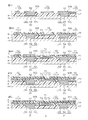
- FIG. 1 is a bottom view of a first embodiment of an image sensor mounting substrate according to the present invention.
- FIG. 2 is a cross-sectional view taken along the line AA of the image sensor mounting substrate shown in FIG. 3A to 3B are cross-sectional views of only the image sensor connection terminal of the image sensor mounting substrate shown in FIG. 2, and
- FIG. 3A illustrates the peripheral portion and the solid portion of the terminal connection portion of the image sensor connection terminal in phantom lines.
- FIG. 3B shows a diagram in which the inner side portion and the outer side portion are indicated by virtual lines in the image sensor connection terminal.
- 4A to 4E show manufacturing process diagrams of the image sensor mounting substrate shown in FIG. 1, FIG. 4A is a metal support plate preparation process, FIG.
- FIG. 4B is a base insulating layer formation process
- FIG. 4C is a metal thin film formation process
- 4D shows a photoresist forming process
- FIG. 4E shows a conductor pattern forming process.
- 5F to FIG. 5J show manufacturing process diagrams of the imaging element mounting substrate shown in FIG. 1 following FIG. 4,
- FIG. 5F shows a photoresist / metal thin film removing process
- FIG. 5G shows a first cover insulating layer forming process.
- 5H shows a shield layer forming step
- FIG. 5I shows a second cover insulating layer forming step
- FIG. 5J shows a metal support plate removing step.
- FIG. 6 shows an imaging apparatus including the imaging element mounting substrate shown in FIG. FIG.
- FIG. 7 is a schematic diagram when the imaging element is mounted on the imaging element mounting substrate shown in FIG.
- FIG. 8A to FIG. 8B are schematic diagrams when the image pickup device is mounted on the image pickup device mounting substrate in which the solid portion is not filled in the image pickup device opening
- FIG. 8A is an image pickup device mounting substrate before mounting
- 8B shows the imaging apparatus after mounting.
- 9A to 9B are schematic diagrams when the image pickup device is mounted on the cover-lay-bonded image pickup device mounting substrate, FIG. 9A is the image pickup device mounting substrate before mounting, and FIG. 9B is the image pickup device after mounting. Indicates.
- FIG. 9A is the image pickup device mounting substrate before mounting
- FIG. 9B is the image pickup device after mounting. Indicates.
- FIG. 9A is the image pickup device mounting substrate before mounting
- FIG. 9B is the image pickup device after mounting. Indicates.
- FIG. 9A is the image pickup device mounting substrate before mounting
- FIG. 9B is the image pickup device after mounting. Indicates.
- FIG. 10 shows a cross-sectional view of a modification of the first embodiment of the imaging element mounting substrate of the present invention (a form in which a minute recess is formed on the upper surface).
- FIG. 11 shows a cross-sectional view of a modification of the first embodiment of the imaging element mounting substrate of the present invention (a form not including a shield layer and a second cover insulating layer).
- FIG. 12 shows a side sectional view of the second embodiment of the image sensor mounting substrate of the present invention.
- 13A to 13B are cross-sectional views of only the image sensor connection terminal of the image sensor mounting substrate shown in FIG. 12, and FIG. 13A shows a peripheral portion and a solid portion of the terminal connection portion of the image sensor connection terminal as virtual lines.
- FIG. 13A shows a peripheral portion and a solid portion of the terminal connection portion of the image sensor connection terminal as virtual lines.
- FIG. 13B shows a diagram in which the inner side and the outer side are indicated by imaginary lines in the image sensor connection terminal.
- 14A to 14E show manufacturing process diagrams of the imaging element mounting substrate shown in FIG. 12, FIG. 14A is a gold plating layer forming process, FIG. 14B is a filling part forming process, and FIG. 14C is a metal thin film forming process.
- FIG. 14D shows a photoresist forming process, and FIG. 14E shows a conductor pattern forming process.
- 15F to FIG. 15J show manufacturing process diagrams of the imaging element mounting substrate shown in FIG. 12 following FIG. 14, FIG. 15F shows a photoresist / metal thin film removing step, and FIG. 15G shows a first cover insulating layer forming step.
- FIG. 15H shows a shield layer forming step
- FIG. 15I shows a second cover insulating layer forming step
- FIG. 15J shows a metal support plate removing step.
- FIG. 16 shows a cross-sectional view of a modification of the second embodiment of the image sensor mounting substrate of the present invention (a form not including a shield layer and a second cover insulating layer).
- FIG. 17 shows a modification of the second embodiment of the image sensor mounting substrate of the present invention (a mode in which the shield layer and the second cover insulating layer are not provided).
- the vertical direction of the paper is the front-back direction (first direction)
- the upper side of the paper is the front side (one side in the first direction)
- the lower side of the paper surface is the rear side (the other side in the first direction).
- the left-right direction on the paper surface is the left-right direction (second direction orthogonal to the first direction)
- the left side of the paper surface is the left side (second side in the second direction)
- the right side of the paper surface is the right side (the other side in the second direction).
- the paper thickness direction is the vertical direction (thickness direction, third direction orthogonal to the first direction and the second direction), the back side of the paper is the upper side (one side in the thickness direction, the third direction one side), and the front side of the paper is The lower side (the other side in the thickness direction, the other side in the third direction). Specifically, it conforms to the direction arrow in each figure.
- ⁇ First Embodiment> 1. Image Sensor Mounting Board With reference to FIGS. 1 to 3B, a first embodiment of an image sensor mounting board (hereinafter also simply referred to as a mounting board) will be described as an embodiment of the wired circuit board of the present invention.
- the mounting substrate 1 of the first embodiment is a flexible printed circuit board (FPC) for mounting an image sensor 21 (described later), and does not yet include the image sensor 21.
- the mounting substrate 1 has a flat plate shape (sheet shape) having a substantially rectangular shape (rectangular shape) in plan view extending in the front-rear direction and the left-right direction (plane direction).
- the mounting substrate 1 includes a housing arrangement portion 2 and an external component connecting portion 3 as shown in FIG.
- the housing arrangement part 2 is a part where a housing 22 (described later) and an image sensor 21 are arranged. Specifically, when the housing 22 is disposed on the mounting substrate 1, it is a portion overlapping with the housing 22 when projected in the thickness direction. A plurality of image sensor connection terminals 9 (described later) for electrical connection with the image sensor 21 are arranged at a substantially central portion of the housing arrangement portion 2. In addition, the housing arrangement
- the external component connecting portion 3 is an area other than the housing arrangement portion 2 and is a portion for connecting to an external component.
- the external component connection portion 3 is arranged on the rear side of the housing arrangement portion 2 such that the front end edge of the external component connection portion 3 is continuous with the rear end edge of the housing arrangement portion 2.
- a plurality of external component connection terminals 10 (described later) for electrical connection with external components are arranged on the rear edge of the external component connection portion 3.
- the mounting substrate 1 includes a base insulating layer 4 as a first insulating layer, a conductor pattern 5, a first cover insulating layer 6 as a second insulating layer, a shield layer 7, and a third layer. And a second insulating cover layer 8 as an insulating layer.
- the mounting substrate 1 includes only the base insulating layer 4, the conductor pattern 5, the first cover insulating layer 6, the shield layer 7, and the second cover insulating layer 8.
- the base insulating layer 4 has an outer shape of the mounting substrate 1 and is formed in a substantially rectangular shape in bottom view.
- the lower surface (the other surface in the thickness direction) of the insulating base layer 4 is formed to be substantially flat.
- a plurality of imaging element openings 41 (openings) and a plurality of external component openings 42 are formed.
- the plurality of imaging element openings 41 are openings for exposing the imaging element connection terminals 9 from the lower surface.
- the plurality of image sensor opening portions 41 are arranged at intervals in the center portion of the housing arrangement portion 2 so as to form a rectangular frame shape.
- the imaging element opening 41 penetrates the base insulating layer 4 in the thickness direction and has a substantially circular shape in a bottom view.
- the imaging element opening 41 has a shape in which the opening cross-sectional area increases toward the upper side. That is, the image sensor opening 41 has a tapered shape that becomes wider as it goes upward (becomes narrower as it goes downward) in a side sectional view.
- the image sensor opening 41 is partitioned from the inner side surface 43 of the base insulating layer 4, and an angle formed by the inner side surface 43 of the base insulating layer 4 and the lower surface of the image sensor opening 41 is, for example, in a side sectional view. , 100 ° or more, preferably 120 ° or more, and for example, 170 ° or less, preferably 160 ° or less.
- the metal thin film 17 can be formed uniformly in the image sensor opening 41, and the taper-shaped image sensor connection terminal 9 can be reliably formed.
- the plurality of external component openings 42 are openings for exposing the external component connection terminals 10 from the lower surface.
- the external component openings 42 are aligned and arranged at the rear end edge of the external component connection portion 3 at intervals in the left-right direction.
- the external component opening 42 penetrates the insulating base layer 4 in the thickness direction and has a substantially rectangular shape (rectangular shape) when viewed from the bottom.
- the external component opening 42 is formed so as to extend from the rear end edge of the external component connecting portion 3 toward the front side in a bottom view.
- the base insulating layer 4 is made of an insulating material.
- the insulating material include synthetic resins such as polyimide resin, polyamideimide resin, acrylic resin, polyethernitrile resin, polyethersulfone resin, polyethylene terephthalate resin, polyethylene naphthalate resin, and polyvinyl chloride resin.
- the base insulating layer 4 is made of a polyimide resin.
- the thickness T 1 of the base insulating layer 4 is, for example, 1 ⁇ m or more, preferably 3 ⁇ m or more, more preferably 5 ⁇ m or more, and for example, 30 ⁇ m or less, preferably 10 ⁇ m or less, more preferably 8 ⁇ m or less. is there.
- the conductor pattern 5 is provided on the upper side of the insulating base layer 4 so as to be in contact with the upper surface (one surface in the thickness direction) of the insulating base layer 4.
- the conductor pattern 5 includes a plurality of image sensor connection terminals 9 (terminals), a plurality of external component connection terminals 10, and a plurality of wirings 11.
- the plurality of image sensor connection terminals 9 are aligned and arranged at intervals in the center of the housing arrangement portion 2 so as to form a rectangular frame. That is, the plurality of image sensor connection terminals 9 are provided so as to correspond to a plurality of terminals 25 (described later) of the image sensor 21 to be mounted. The plurality of image sensor connection terminals 9 are provided corresponding to the plurality of image sensor openings 41.
- the image sensor connection terminal 9 has a substantially inverted hat shape in cross section, and is integrally provided with a terminal connection portion 51 and a wiring connection portion 52 disposed thereon.
- the terminal connection part 51 is a part connected to a solder bump 26 (described later), and forms the lower part of the image sensor connection terminal 9.
- the terminal connection portion 51 is disposed inside the image sensor opening 41.
- the terminal connection part 51 has a shape in which the opening cross-sectional area widens toward the upper side.
- the terminal connection portion 51 has a tapered shape that becomes wider as it goes upward (becomes narrower as it goes downward) in a side sectional view.
- the terminal connection portion 51 has a substantially circular shape when viewed from the bottom, and has a substantially truncated cone shape that increases in diameter toward the upper side (reduces toward the lower side).
- the terminal connection part 51 is integrally provided with the peripheral part 53 and the solid part 54 arrange
- the peripheral edge 53 is in contact with the inner side surface 43 that forms the imaging element opening 41 of the base insulating layer 4, and forms an outer shape in the surface direction of the terminal connection portion 51. That is, the peripheral portion 53 has a hollow substantially truncated cone shape.
- the solid part 54 is formed integrally with the peripheral part 53 inside the peripheral part 53. That is, the outer peripheral edge of the solid portion 54 is continuous with the inner peripheral edge of the peripheral portion 53.
- the solid part 54 has a solid substantially truncated cone shape.
- the peripheral portion 53 and the solid portion 54 fill (fill) the entire image sensor opening 41 as shown in FIG. That is, the shape of the terminal connection portion 51 including the peripheral portion 53 and the solid portion 54 matches the shape of the image sensor opening portion 41, and the thickness thereof is the same as the thickness of the base insulating layer 4.
- the lower surface (exposed surface) of the terminal connection portion 51 is exposed from the image sensor opening 41 and is formed to be substantially flat. Specifically, the lower surface of the terminal connection portion 51 is substantially flush with the lower surface of the base insulating layer 4. That is, the vertical displacement (step) is not completely generated between the lower surface of the terminal connection portion 51 and the lower surface of the base insulating layer 4, or the step is, for example, 2.0 ⁇ m or less in the vertical direction, preferably 1.0 ⁇ m or less, more preferably 0.5 ⁇ m or less.
- the wiring connection part 52 is a part that is continuous with the connection wiring 12 in the surface direction, and forms the upper part of the image sensor connection terminal 9.
- the wiring connection portion 52 has a substantially circular flat plate shape when viewed from the bottom, and includes the terminal connection portion 51 when projected in the thickness direction. That is, the peripheral edge of the wiring connection part 52 is located outside the peripheral edge of the terminal connection part 51 in the surface direction (front-rear direction and left-right direction).
- the lower surface of the inner peripheral portion of the wiring connection portion 52 is integrally continuous with the upper surface of the terminal connection portion 51 in the vertical direction.
- the lower surface of the outer peripheral portion of the wiring connection portion 52 is in contact with the upper surface of the base insulating layer 4.
- the image sensor connection terminal 9 extends outward from the inner portion 55 and the inner portion 55 included in the outermost shape of the image sensor opening 41 when projected in the vertical direction, as referred to by the imaginary line in FIG. 3B.
- An outer portion 56 (a collar portion) is integrally provided. That is, in the image sensor connection terminal 9, the terminal connection portion 51 and the inner peripheral portion of the wiring connection portion 52 that is continuous with the terminal connection portion 51 in the vertical direction correspond to the inner side portion 55, and the upper surface of the base insulating layer 4. The peripheral edge portion of the wiring connection portion 52 that is in contact corresponds to the outer side portion 56.
- the upper surface of the image sensor connection terminal 9 (that is, the upper surface of the wiring connection portion 52) is formed to be substantially flat. Specifically, the upper surface of the inner portion 55 is substantially flush with the upper surface of the outer portion 56. That is, there is no vertical displacement (step) between the upper surface of the inner portion 55 and the upper surface of the outer portion 56, or the step is, for example, 2.0 ⁇ m or less in the vertical direction, preferably 1.0 ⁇ m or less, more preferably 0.5 ⁇ m or less.
- a region in plan view or bottom view that overlaps with the image sensor connection terminal 9 is defined as a terminal region 14.
- the plurality of external component connection terminals 10 are arranged at the rear end edge of the external component connection portion 3 so as to be spaced apart from each other in the left-right direction. That is, it is provided so as to correspond to a plurality of terminals (not shown) of the external component.
- the plurality of external component connection terminals 10 are provided corresponding to the plurality of external component openings 42.
- the external component connection terminal 10 has a substantially rectangular shape (rectangular shape) in plan view.
- the external component connection terminal 10 is disposed in the external component opening 42 and its lower surface is exposed from the external component opening 42.
- the plurality of wirings 11 include a plurality of connection wirings 12 and a plurality of ground wirings 13 as shown in FIG.
- connection wiring 12 is integrally formed with the image sensor connection terminal 9 and the external component connection terminal 10 so as to connect them. That is, one end of the connection wiring 12 is continuous with the wiring connection portion 52 of the image sensor connection terminal 9 in the surface direction, and the other end of the connection wiring 12 is continuous with the external component connection terminal 10 in the surface direction. Connected.
- the upper surface of the connection wiring 12 is formed to be substantially flush with the upper surface of the wiring connection portion 52. That is, there is no vertical displacement (step) between the upper surface of the connection wiring 12 and the upper surface of the wiring connection portion 52, or the step is, for example, 2.0 ⁇ m or less in the vertical direction, preferably 1.0 ⁇ m or less, more preferably 0.5 ⁇ m or less.
- the plurality of ground wirings 13 are provided so as to correspond to the plurality of connection wirings 12. Specifically, the plurality of ground wirings 13 are provided along the plurality of connection wirings 12. The upper surface of the ground wiring 13 is at the same vertical position as the upper surface of the connection wiring 12, and the lower surface of the ground wiring 13 is at the same vertical position as the lower surface of the connection wiring 12. A ground terminal (not shown) is integrally connected to one end of the ground wiring 13.
- Examples of the material of the conductor pattern 5 include metal materials such as copper, silver, gold, nickel, alloys containing them, and solder. Preferably, copper is used.
- the thickness T 2 of the imaging element connection terminals 9 (terminal connecting portion 51 and the wiring connecting part 52) and the external component connection terminals 10, respectively for example, 2 [mu] m or more, preferably, 5 [mu] m or more, more preferably at 7 ⁇ m or more, For example, it is 30 ⁇ m or less, preferably 20 ⁇ m or less, and more preferably 15 ⁇ m or less.
- the thickness T 3 of the wiring 11 is, for example, 1 ⁇ m or more, preferably 3 ⁇ m or more, and for example, 15 ⁇ m or less, preferably 10 ⁇ m or less, more preferably 8 ⁇ m or less, and further preferably 5 ⁇ m or less.
- the width of the image sensor connection terminal 9, that is, the length L (diameter) in the surface direction of the terminal region 14 is, for example, 30 ⁇ m or more, preferably 50 ⁇ m or more, and, for example, 500 ⁇ m or less, preferably 200 ⁇ m or less. is there.
- the width of the wiring 11 is, for example, 5 ⁇ m or more, preferably 10 ⁇ m or more, and for example, 100 ⁇ m or less, preferably 50 ⁇ m or less.
- the first insulating cover layer 6 is provided above the insulating base layer 4 and the conductive pattern 5 so as to cover the conductive pattern 5. That is, the first insulating cover layer 6 is disposed so as to come into contact with the upper and side surfaces of the conductor pattern 5 and the upper surface of the insulating base layer 4 exposed from the conductive pattern 5. The vertical position of the lower surface of the first insulating cover layer 6 coincides with the vertical position of the lower surface of the wiring 11 and the vertical position of the upper surface of the insulating base layer 4.
- the first cover insulating layer 6 has an outer shape in plan view that is the same as that of the base insulating layer 4 except for the portion where the external component connection terminal 10 is formed.
- the first cover insulating layer 6 has a ground opening 61.
- the ground opening 61 is an opening for exposing the upper surface of the ground wiring 13.
- the ground opening 61 is formed so as to overlap with the ground wiring 13 when projected in the thickness direction.
- the ground opening 61 penetrates the first cover insulating layer 6 in the thickness direction and has a substantially circular shape when viewed from the bottom.
- the ground opening 61 has a tapered shape that becomes narrower toward the lower side in a side sectional view.
- the first cover insulating layer 6 is formed of an insulating material similar to the insulating material described above for the base insulating layer 4, and is preferably formed of a polyimide resin.
- the thickness T 4 of the first insulating cover layer 6 is, for example, 1 ⁇ m or more, preferably 2 ⁇ m or more, and for example, 30 ⁇ m or less, preferably 10 ⁇ m or less, more preferably 5 ⁇ m or less.
- the shield layer 7 is disposed on the upper side of the first cover insulating layer 6 so as to be in contact with the upper surface of the first cover insulating layer 6.
- the shield layer 7 is a layer that shields electromagnetic waves from the outside, and is formed in a sheet shape extending in the surface direction (front-rear direction and left-right direction).
- the shield layer 7 is electrically connected to the ground wiring 13. That is, the shield layer 7 is continuous with the ground wiring 13 in the ground opening 61. Specifically, the shield layer 7 includes a contact portion 71 that has a convex shape on the lower side and is in contact with the upper surface of the ground wiring 13 at a portion facing the ground wiring 13.
- the contact portion 71 includes a flat portion 72 that is in direct contact with the ground wiring 13 and an inclined portion 73 that is integrally disposed so as to be continuous around the flat portion 72.
- the flat part 72 is formed in a flat plate shape extending in the surface direction.
- the inclined portion 73 extends in an inclination direction intersecting (inclining) in the vertical direction and the surface direction.
- the angle between the flat portion 72 and the inclined portion 73 is, for example, 100 ° or more, preferably 120 ° or more, and for example, 170 ° or less, preferably 160 ° or less.
- the shield layer 7 is grounded via the ground wiring 13.
- the shield layer 7 is made of a conductor, and for example, a metal material such as copper, chromium, nickel, gold, silver, platinum, palladium, titanium, tantalum, solder, or an alloy thereof is used. Preferably, copper is used.
- the thickness T 5 of the shield layer 7 is, for example, 0.05 ⁇ m or more, preferably 0.1 ⁇ m or more, and for example, 3 ⁇ m or less, preferably 1 ⁇ m or less.
- the second cover insulating layer 8 is provided on the upper side of the shield layer 7 so as to cover the entire surface of the shield layer 7.
- the outer shape of the second cover insulating layer 8 is formed to be the same as that of the first cover insulating layer 6.
- the thickness T 6 of the second insulating cover layer 8 is, for example, 1 [mu] m or more, preferably not 2 ⁇ m or more, and is, for example, 30 [mu] m or less, preferably, 10 [mu] m or less, more preferably 5 ⁇ m or less.
- the total thickness T 7 of the mounting board 1 is, for example, 7 [mu] m or more, preferably not less 10 ⁇ m or more, and is, for example, 50 [mu] m or less, preferably 30 ⁇ m or less.
- the upper surface 14a of the terminal region 14 is formed so that the entire surface thereof is substantially flat.
- the vertical displacement of the upper surface 14a of the terminal region 14 with respect to a line connecting both ends (points A and B in FIG. 2) of the upper surface 14a of the terminal region 14 is, for example, 3.0 ⁇ m or less, preferably Is 2.0 ⁇ m or less, more preferably 1.0 ⁇ m or less, and still more preferably 0.5 ⁇ m or less.
- the vertical distance between a line connecting both ends (points A and B in FIG. 2) of the upper surface 14a of the terminal region 14 and the lower surface (point C) at the center in the surface direction of the solid portion 54 is, for example, 3.0 ⁇ m.
- the thickness is preferably 2.0 ⁇ m or less, more preferably 1.0 ⁇ m or less, and still more preferably 0.5 ⁇ m or less.
- the amount of change in the total thickness of the mounting substrate 1 in the terminal region 14 is, for example, 3.0 ⁇ m or less, preferably 2.0 ⁇ m or less, more preferably 1.0 ⁇ m or less, and even more preferably 0.5 ⁇ m or less.
- the amount of change is based on the thickness of the edge of the terminal region 14 in the surface direction (points A and B in FIG. 2). For example, the difference in thickness between the both end edges and the surface center point (point C in FIG. 2) is within the above range.
- the mounting board 1 of the first embodiment includes, for example, a metal support plate preparation process, a base insulating layer formation process, a metal thin film formation process, and a photoresist formation process.
- the conductive pattern forming step, the photoresist / metal thin film removing step, the first cover insulating layer forming step, the shield layer forming step, the second cover insulating layer forming step, and the metal support plate removing step are sequentially performed. It is done.
- a metal support plate 16 is prepared as shown in FIG. 4A.
- the metal support plate 16 is made of a metal material such as stainless steel, 42 alloy, aluminum, or copper alloy, for example.
- the metal support plate 16 is made of stainless steel.
- the thickness of the metal support plate 16 is, for example, 5 ⁇ m or more, preferably 10 ⁇ m or more, for example, 50 ⁇ m or less, preferably 30 ⁇ m or less.
- the upper surface of the metal support plate 16 is formed to be flat (smooth).
- the base insulating layer 4 is formed on the upper surface of the metal support plate 16 as shown in FIG. 4B. That is, the base insulating layer 4 having openings (the image sensor opening 41 and the external component opening 42) is formed on the upper surface of the metal support plate 16.
- a varnish of a photosensitive insulating material (for example, photosensitive polyimide) is applied to the entire upper surface of the metal support plate 16 and dried to form a base film (base insulating layer). Thereafter, the base film is exposed through a photomask having a pattern corresponding to the openings (the image sensor opening 41 and the external component opening 42).
- the tapered shape can be formed by adjusting the parallelism of light by an exposure gap at the time of exposure. Thereafter, the base film is developed and, if necessary, cured by heating.
- the metal thin film 17 (seed film) is formed on the upper surface of the base insulating layer 4 and the upper surface of the metal support plate 16 exposed from the image sensor opening 41 and the external component opening 42. ).
- the metal thin film 17 for example, a metal material such as copper, chromium, nickel, titanium and alloys thereof is used.
- chromium is used from the viewpoint of adhesion to the base insulating layer 4.
- the metal thin film 17 is formed, for example, by performing a thin film forming method such as sputtering or plating on the base insulating layer 4 formed on the metal support plate 16.
- a thin film forming method such as sputtering or plating
- the metal thin film 17 is formed by sputtering.
- the thickness of the metal thin film 17 is, for example, 10 nm or more, preferably 20 nm or more, and, for example, 300 nm or less, preferably 150 nm or less.
- a photoresist 18 is formed on the metal thin film 17 as shown in FIG. 4D. That is, a photoresist 18 having an opening corresponding to the conductor pattern 5 is formed.
- a dry film resist is disposed on the entire upper surface of the metal thin film 17. Thereafter, the dry film resist is exposed through a photomask having a pattern corresponding to the conductor pattern 5. Thereafter, the dry film resist is developed and, if necessary, heat-cured to form the photoresist 18 as a plating resist.
- the metal thin film 17 corresponding to the conductor pattern 5 is exposed from the photoresist 18.
- the conductor pattern 5 is formed on the surface of the metal thin film 17 exposed from the photoresist 18 as shown in FIG. 4E.
- electrolytic plating in which power is supplied from the metal thin film 17 is performed.
- the via fill plating method is adopted.
- a plating bath preferably a copper sulfate plating bath
- an inhibitor that suppresses plating growth and an accelerator that promotes plating growth is used.
- the plating layer 19 is formed so as to fill the entire imaging element opening 41. That is, in the image pickup device opening 41, a terminal connection portion 51 integrally including a peripheral edge portion 53 and a solid portion 54 is formed, and a wiring connection portion 52 is formed integrally thereon. Further, the upper surface of the wiring connection portion 52 is formed so as to be flush with the upper surface of the wiring 11. As a result, the conductor pattern 5 having the image sensor connection terminal 9, the external component connection terminal 10, and the wiring 11 is formed.
- the metal thin film 17 corresponding to the conductor pattern 5 is integrated with the plating layer 19 by electrolytic plating to form the conductor pattern 5 together with the plating layer 19. That is, in FIG. 4D to FIG. 5H, the image pickup device connection terminal 9 and the wiring 11 are shown to be two layers of the plating layer 19 and the metal thin film 17, respectively. When the material of the metal thin film 17 is the same, it may be completely integrated into one layer (see FIG. 2).
- the photoresist 18 and the metal thin film 17 are removed.
- the remaining photoresist 18 is removed. For example, it is removed by wet etching. Thereafter, the metal thin film 17 facing the remaining photoresist 18 is removed. For example, it is removed by peeling or wet etching.
- the first cover insulating layer 6 is disposed on the upper surfaces of the conductor pattern 5 and the base insulating layer 4 as shown in FIG. 5G.
- the first cover insulating layer 6 having the ground opening 61 is formed so that the upper surface of the ground wiring 13 of the conductor pattern 5 is exposed.
- the first cover insulating layer 6 is formed so that the ground opening 61 has a tapered shape that becomes narrower toward the lower side in a side sectional view.
- the shield layer 7 is formed on the first insulating cover layer 6 as shown in FIG. 5H.
- Examples of the formation of the shield layer 7 include plating methods such as electrolytic plating and electroless plating, such as sputtering, vapor deposition, and ion plating, such as a coating method using a conductive paste.
- plating methods such as electrolytic plating and electroless plating, such as sputtering, vapor deposition, and ion plating, such as a coating method using a conductive paste.
- sputtering and vapor deposition are mentioned, and sputtering is more preferred.
- the second cover insulating layer 8 is disposed on the upper surface of the shield layer 7 as shown in FIG. 5I.
- the second cover insulating layer 8 is formed on the entire upper surface of the shield layer 7.
- the mounting substrate 1 including the base insulating layer 4, the conductor pattern 5, the first cover insulating layer 6, the shield layer 7, and the second cover insulating layer 8 is supported by the metal support plate 16. Get in.
- the metal support plate 16 is removed as shown in FIG. 5J.
- Examples of the removing method include a method of peeling the metal support plate 16 from the lower surface of the mounting substrate 1, a method of treating the metal support plate 16 by wet etching, and the like.
- the mounting substrate 1 including the base insulating layer 4, the conductor pattern 5, the first cover insulating layer 6, the shield layer 7, and the second cover insulating layer 8 is obtained.
- Such a mounting substrate 1 is used, for example, as a printed circuit board for mounting an image pickup device. That is, the mounting substrate 1 is used for an imaging apparatus such as a camera module.
- Imaging Device With reference to FIG. 6, an imaging device 20 including the mounting substrate 1 of the first embodiment will be described.
- the imaging device 20 includes a mounting substrate 1, an imaging element 21, a housing 22, an optical lens 23, and a filter 24.
- the mounting substrate 1 is used upside down from the state shown in FIG. That is, the mounting substrate 1 is arranged so that the insulating base layer 4 is on the upper side and the second insulating cover layer 8 is on the lower side.
- the imaging element 21 is a semiconductor element that converts light into an electrical signal, and examples thereof include solid-state imaging elements such as a CMOS sensor and a CCD sensor.
- the imaging element 21 is formed in a substantially rectangular flat plate shape in plan view, and includes a silicon such as a Si substrate, a photodiode (photoelectric conversion element), and a color filter arranged on the silicon substrate (not shown).
- a plurality of terminals 25 corresponding to the image sensor connection terminals 9 of the mounting substrate 1 are provided on the lower surface of the image sensor 21.
- the thickness of the image sensor 21 is, for example, 10 ⁇ m or more, preferably 50 ⁇ m or more, and for example, 1000 ⁇ m or less, preferably 500 ⁇ m or less.
- the image sensor 21 is mounted on the mounting substrate 1. That is, the terminal 25 of the image sensor 21 is flip-chip mounted via the corresponding image sensor connection terminal 9 of the mounting substrate 1 and the solder bump 26. As a result, the image pickup device 21 is arranged at the center of the housing arrangement portion 2 of the mounting substrate 1 and is electrically connected to the image pickup device connection terminal 9 and the external component connection terminal 10 of the mounting substrate 1.
- the imaging element 21 constitutes an imaging unit 27 by being mounted on the mounting substrate 1. That is, the imaging unit 27 includes the mounting substrate 1 and the imaging element 21 mounted thereon.
- the housing 22 is arranged in the housing arrangement part 2 of the mounting substrate 1 so as to surround the imaging element 21 with a space.
- the housing 22 has a substantially rectangular tube shape in plan view.
- a fixing portion for fixing the optical lens 23 is provided at the upper end of the housing 22.
- the optical lens 23 is disposed on the upper side of the mounting substrate 1 with a distance from the mounting substrate 1 and the imaging element 21.
- the optical lens 23 is formed in a substantially circular shape in plan view, and is fixed by a fixing portion so that light from the outside reaches the image sensor 21.
- the filter 24 is disposed at the center of the imaging element 21 and the optical lens 23 in the vertical direction with a space therebetween and is fixed to the housing 22.
- the mounting substrate 1 includes a base insulating layer 4, an image sensor connection terminal 9, a first cover insulating layer 6, and a connection wiring 12.
- the base insulating layer 4 has an imaging element opening 41 that penetrates in the vertical direction and whose opening cross-sectional area increases toward the upper side.
- the image pickup device connection terminal 9 includes a peripheral portion 53 that contacts the inner side surface 43 of the image pickup device opening 41 and a solid portion 54 that is disposed integrally with the peripheral portion 53 inside the peripheral portion 53. The peripheral portion 53 and the solid portion 54 fill the entire image sensor opening 41.
- the terminal region 14 on which the image sensor 21 is mounted is reinforced by the solid portion 54. Therefore, when the mounting substrate 1 is turned upside down and the image pickup device 21 is mounted on the mounting substrate 1 from above, the terminal region 14 of the mounting substrate 1 can be prevented from being deformed downward (see FIG. 7). ). As a result, the inclination of the image sensor 21 with respect to the mounting substrate 1 can be suppressed, and the image sensor 21 can be mounted with high accuracy. Further, since a support substrate such as the metal support plate 16 is not required, the thickness can be reduced.
- a mounting board that includes a peripheral portion 53 but does not include a solid portion 54. More specifically, there is no solid portion 54, and the peripheral portion 53 has an opening at the lower end.
- the recess 15 is formed on the upper surface 14 a of the terminal region 14.
- FIG. 8B when the mounting substrate is turned upside down and the image sensor 21 is mounted on the mounting substrate from above, the terminal region 14 is partially formed due to the stress on the lower side and the presence of the recess 15 at the time of mounting. Deforms downward. As a result, the image sensor 21 is tilted, and the mounting accuracy is lowered.
- a conventional cover-lay adhesive type mounting board that is, a mounting board having a base insulating layer 4, a conductor pattern 5, an adhesive layer 30, and a first cover insulating layer 6.
- the image sensor connection terminal 9 is disposed inside the image sensor opening 41 and is located below the upper surface of the first cover insulating layer 6.
- the solder bump 26 is disposed inside the image pickup device opening 41, and therefore the volume (amount) of the solder bump 26 needs to be increased. Therefore, the variation in the shape and size of each solder bump 26 becomes large. As a result, the imaging element 21 may be tilted and the mounting accuracy may be reduced.
- the size of the image sensor 21 and the number and size of each terminal are changed in order to make the operational effects easier to understand.
- the image sensor opening 41 has an opening cross-sectional area that increases toward the upper side, and the image sensor opening 41 is filled with the image sensor connection terminal 9. Therefore, the image sensor connection terminal 9 has a wide shape in which a cross-sectional area increases toward the upper side, and has a sufficient thickness. Therefore, when the mounting substrate 1 is turned upside down and the image sensor 21 is mounted on the mounting substrate 1 from above, the image sensor connection terminal 9 receives the stress from the upper side to the lower side while dispersing the stress downward. (See FIG. 7). Therefore, damage to the image sensor connection terminal 9 can be suppressed.
- the opening area of the imaging element opening 41 increases toward the upper side, that is, the opening area decreases toward the lower side. Therefore, the area (exposed area) of the terminal connection part 51 exposed from the imaging element opening 41 can be reduced. Therefore, in the case where a plurality of image sensor connection terminals 9 are formed, it is possible to reduce the difference in the variation in the absolute value of the exposed area between the image sensor connection terminals 9. As a result, it is possible to reduce variation in conductivity due to variation in contact area with the terminal 25 of the image sensor 21.
- the lower surface of the image sensor connection terminal 9, that is, the lower surface of the terminal connection portion 51 is substantially flush with the lower surface of the base insulating layer 4.
- the image pickup device 21 and the solder bump 26 are attached to the lower surface 14 b ( At the time of mounting, collision with the base insulating layer 4 around the upper side) can be suppressed. Therefore, the image sensor 21 can be easily mounted on the mounting substrate 1.
- the upper surface 14a of the terminal region 14 is substantially flat. Therefore, as shown in FIG. 7, the upper surface 14a of the terminal region 14 (corresponding to the lower surface in FIG. 7) can be easily brought into contact with the mounting table (not shown) as a whole during mounting, and the terminal region is formed on the upper surface 14a. 14 can be supported. As a result, it is possible to more reliably suppress the vertical deformation in the terminal region 14.
- an out-of-area recess (reference numeral 80 shown in FIG. 2) exists between the plurality of terminal areas 14, and in particular, the upper surface 14 a of the terminal area 14. It is important that is substantially flat. This is because, as shown in FIG. 7, when the image sensor 21 is mounted, the region where the pressure from the image sensor 21 works is substantially only the terminal region 14. That is, since the pressure hardly acts on the out-of-region recess 80, even if the out-of-region recess 80 exists, the influence of the deformation of the terminal region 14 of the mounting substrate 1 and thus the entire mounting substrate 1 in the vertical direction. Is considered virtually non-existent.
- the terminal region 14 can be further reinforced by the wiring connection portion 52. Therefore, it is possible to further suppress the terminal region 14 from being deformed in the vertical direction. Further, since the upper surfaces of the connection wiring 12 and the wiring connection portion 52 are substantially flush with each other, the upper surface of the mounting substrate 1 (the region corresponding to the connection wiring 12 and the region corresponding to the wiring connection 52) can be further flattened. it can. Therefore, it is possible to further suppress the entire mounting substrate 1 from being deformed in the vertical direction.
- the image sensor connection terminal 9 includes an inner portion 55 and an outer portion 56 when projected in the vertical direction. Further, the upper surface of the inner portion 55 is substantially flush with the upper surface of the outer portion 56.
- the upper surface 14a of the terminal region 14 can be further flattened. Therefore, the vertical deformation in the terminal region 14 can be further suppressed.
- the mounting substrate 1 further includes a shield layer 7 disposed on the upper surface of the first cover insulating layer 6 and a second cover insulating layer 8 disposed on the upper surface of the shield layer 7. Therefore, since the electromagnetic wave generated from the outside can be shielded by the shield layer 7, the reliability of the imaging device 20 can be improved.
- the wiring 11 includes a connection wiring 12 and a ground wiring 13, and the shield layer 7 is electrically connected to the ground wiring 13. Therefore, the ground wiring 13 is disposed on the upper surface of the base insulating layer 4, that is, at the same vertical position as the connection wiring 12. Therefore, it is not necessary to separately provide a layer for providing the ground wiring 13. As a result, the mounting substrate 1 can be thinned.
- the mounting substrate 1 is an adhesiveless mounting substrate in which each layer (the base insulating layer 4, the conductor pattern 5, the first cover insulating layer 6, the shield layer 7, and the second cover insulating layer 8) is in direct contact. Therefore, it is possible to reduce the thickness (lower height).
- the adhesive layer 30 such as an acrylic adhesive is not required, deterioration of the adhesive layer 30 due to wet heat can be suppressed, and the heat and moisture resistance is excellent.
- the method for manufacturing the mounting substrate 1 it is possible to manufacture the mounting substrate 1 with good mounting accuracy.
- the manufacturing method includes a metal support plate preparation step, a base insulating layer forming step, a metal thin film forming step, a photoresist forming step, a conductor pattern forming step, a photoresist / metal thin film removing step, a first cover insulating layer forming step, A shield layer forming step, a second cover insulating layer forming step, and a metal support plate removing step;
- the mounting substrate 1 is manufactured on the hard metal support plate 16, the handling is easy. Even if the thickness of the insulating base layer 4 is reduced, the metal support plate 16 supports the insulating base layer 4, so that the wiring 11, the first cover insulating layer 6 and the like can be reliably disposed on the insulating base layer 4. . As a result, it is possible to reduce the thickness of the insulating base layer 4 and thus to reduce the thickness of the mounting substrate 1.
- the insulating base layer 4, the first insulating cover layer 6 and the insulating second cover layer 8 are formed using a photosensitive insulating material, the insulating base material 4, the conductive pattern 5, the insulating first cover layer 6,
- the adhesive layer 30 is not required between the shield layer 7 and the second cover insulating layer 8, and these can be laminated. Therefore, it is possible to improve the heat resistance and further reduce the thickness.
- the imaging device 20 the downward deformation in the terminal region 14 of the mounting substrate 1 is suppressed. Therefore, the image sensor 21 is mounted on the mounting substrate 1 with high accuracy, and the connection reliability is excellent. Further, since a support substrate such as the metal support plate 16 is not required, the thickness can be reduced.
- the upper surface 14a of the terminal region 14 is formed so that the entire surface thereof is substantially flat.
- a part may form the micro recessed part 81, and does not need to be substantially flat.
- the upper surface of the inner portion 55 is not substantially flush with the upper surface of the outer portion 56 and is positioned below the upper surface of the outer portion 56.
- the depth of the minute recess 81 is shallower than the depth of the out-of-region recess 80. That is, the bottom of the minute recess 81 is positioned above the bottom of the out-of-region recess 80.
- the embodiment shown in FIG. 10 also has the same operational effects as the embodiment shown in FIG.
- the mounting substrate 1 includes a base insulating layer 4, a conductor pattern 5, a first cover insulating layer 6, a shield layer 7, and a second cover insulating layer 8.
- the mounting substrate 1 may not include the shield layer 7 and the second cover insulating layer 8.
- the mounting substrate 1 shown in FIG. 11 is preferably composed of only the base insulating layer 4, the conductor pattern 5, and the first cover insulating layer 6. At this time, the first insulating cover layer 6 is disposed on the entire upper surface of the conductor pattern 5 and the entire upper surface of the insulating base layer 4 exposed from the conductive pattern 5.
- the embodiment shown in FIG. 11 also has the same operational effects as the embodiment shown in FIG. 11
- the embodiment shown in FIG. 2 is preferable.
- the conductor pattern 5 (the image sensor connection terminal 9, the external component connection terminal 10, and the wiring 11) is formed by integrating the material of the plating layer 19 and the material of the metal thin film 17, respectively.
- the material of the plating layer 19 and the material of the metal thin film 17 are separate, and the conductor pattern 5 includes the plating layer 19 and the metal thin film 17.
- a two-layer structure may be provided.
- the plating layer 19 is made of copper
- the metal thin film 17 is made of chromium.
- the peripheral portion 53 includes a chromium metal thin film disposed on the outer side in the surface direction and a copper metal portion disposed on the inner side.
- the solid part 54 includes a chromium metal thin film disposed on the lower side and a copper metal part disposed on the upper side.
- the shield layer 17 is provided in the embodiment shown in FIG. 2, for example, although not shown, the shield layer 17 may be a second conductor layer such as a wiring and a terminal.
- the thickness of the second conductor layer is, for example, 1 ⁇ m or more, preferably 3 ⁇ m or more, and for example, 15 ⁇ m or less, preferably 10 ⁇ m or less, more preferably 8 ⁇ m or less, and further preferably 5 ⁇ m or less. It may not be electrically connected to the ground wiring 13.
- the second conductor layer can be preferably formed by a plating method such as electrolytic plating.
- the wiring 11 includes the ground wiring 13.
- the ground wiring 13 may not be provided. That is, the wiring 11 can also be configured only from the connection wiring 12.
- the imaging device 21 is flip-chip mounted on the mounting substrate 1.
- the imaging device 21 is wired to the mounting substrate 1. It can also be mounted by bonding.
- Second Embodiment 1 Imaging Device Mounting Board
- a second embodiment of a mounting board will be described as an embodiment of the wired circuit board of the present invention with reference to FIG.
- the same members as those in the first embodiment shown in FIG. 2 described above are denoted by the same reference numerals, and the description thereof is omitted.
- the image sensor connection terminal 9 does not include a gold plating layer.
- the image sensor connection terminal 9 includes a gold plating layer 57. ing.
- the image sensor connection terminal 9 includes a terminal connection portion 51 and a wiring connection portion 52 disposed thereon.
- the terminal connection portion 51 includes a gold plating layer 57 and a filling portion 58 disposed on the gold plating layer 57.
- the gold plating layer 57 is disposed in the image sensor opening 41 and forms the lowermost portion of the terminal connection portion 51.
- the lower surface (exposed surface) of the gold plating layer 57 is exposed from the image sensor opening 41 and is substantially flush with the lower surface of the base insulating layer 4.
- the thickness of the gold plating layer 57 is, for example, 10 nm or more, preferably 20 nm or more, and, for example, 500 nm or less, preferably 300 nm or less, more preferably 150 nm or less.
- the filling portion 58 is provided on the upper side of the gold plating layer 57 so as to be in contact with the upper surface of the gold plating layer 57.
- the upper surface of the filling portion 58 is substantially flush with the upper surface of the base insulating layer 4. That is, there is no vertical displacement (step) in the upper surface of the filling portion 58 and the upper surface of the base insulating layer 4, or the step is, for example, 2.0 ⁇ m or less in the vertical direction, preferably 1.0 ⁇ m or less, more preferably 0.5 ⁇ m or less.
- the material of the filling portion 58 is preferably copper or nickel.
- the imaging element connection terminal 9 is excellent in conductivity.
- the material of the filling part 58 is nickel, it is excellent in the hardness of the image pick-up element connection terminal 9, and the damage of the image pick-up element connection terminal 9 can be suppressed further.
- the thickness of the filling portion 58 is, for example, 1 ⁇ m or more, preferably 3 ⁇ m or more, and for example, 30 ⁇ m or less, preferably 10 ⁇ m or less.
- the gold plating layer 57 and the filling portion 58 fill the entire image sensor opening 41.
- the terminal connection portion 51 includes a peripheral portion 53 and a solid portion 54 disposed inside the peripheral portion 53 as referred to by the phantom line in FIG. 13A.
- 53 and the solid portion 54 fill the entire image sensor opening 41.
- the peripheral portion 53 and the solid portion 54 that fill the imaging element opening 41 are composed of a gold plating layer 57 and a filling portion 58, and the peripheral portion in the surface direction of the gold plating layer 57 and the filling portion 58.
- the peripheral portion in the surface direction corresponds to the peripheral portion 53 of the terminal connection portion 51
- the inner portion in the surface direction of the gold plating layer 57 and the inner portion in the surface direction of the filling portion 58 correspond to the solid portion 54 of the terminal connection portion 51.
- the wiring connection part 52 includes the metal thin film 17 and a wiring connection main body part 59 arranged on the upper side thereof.
- the metal thin film 17 is the metal thin film 17 described above in the first embodiment.
- the lower surface of the inner peripheral portion of the metal thin film 17 is continuous with the upper surface of the terminal connection portion 51 (filling portion 58) in the vertical direction, and the lower surface of the outer peripheral portion of the metal thin film 17 is in contact with the upper surface of the base insulating layer 4. Yes.
- the wiring connection main body 59 coincides with the metal thin film 17 when projected in the thickness direction.
- the thickness of the wiring connection main body 59 is, for example, 1 ⁇ m or more, preferably 3 ⁇ m or more, and for example, 15 ⁇ m or less, preferably 10 ⁇ m or less, more preferably 8 ⁇ m or less.
- the material of the wiring connection main body 59 includes the material of the conductor pattern 5, and preferably copper from the viewpoint of conductivity.
- the imaging element connection terminal 9 includes a gold plating layer 57, a filling portion 58, a metal thin film 17, and a wiring connection main body portion 59 in order from the bottom.
- the image sensor connection terminal 9 is an inner portion included in the outermost shape of the image sensor opening 41 when projected in the vertical direction as referred to by the virtual line in FIG. 13B.
- 55 and an outer portion 56 (a collar portion) extending outward from the inner portion 55 are integrally provided. That is, in the image sensor connection terminal 9, the terminal connection portion 51 (the gold plating layer 57 and the filling portion 58) and the wiring connection portion 52 (the metal thin film 17 and the wiring connection main body portion 59) that are continuous with the terminal connection portion 51 in the vertical direction.
- the inner peripheral portion corresponds to the inner portion 55, and the peripheral portion of the wiring connection portion 52 that is in contact with the upper surface of the base insulating layer 4 corresponds to the outer portion 56.
- the lower surface (exposed surface) of the terminal connection portion 51 that is, the lower surface of the gold plating layer 57 is substantially flush with the lower surface of the base insulating layer 4.
- the upper surface of the inner portion 55 is substantially flush with the upper surface of the outer portion 56.
- the plurality of wirings 11 include a plurality of connection wirings 12 and a plurality of ground wirings 13 as shown in FIG.
- Each of the plurality of wirings 11 includes a metal thin film 17 at the bottom thereof. That is, the plurality of wirings 11 (connection wirings 12 and ground wirings 13) include the metal thin film 17 and the wiring main body portion 60 disposed on the upper side thereof.
- the thickness of the wiring main body portion 60 is the same as the thickness of the wiring connection main body portion 59, for example, 1 ⁇ m or more, preferably 3 ⁇ m or more, and for example, 15 ⁇ m or less, preferably 10 ⁇ m or less, more preferably 8 ⁇ m or less.
- the upper surface of the connection wiring 12 is flush with the upper surface of the wiring connection portion 52. Further, the upper surface 14a of the terminal region 14 is substantially flat.
- the mounting board 1 of the second embodiment includes, for example, a metal support plate preparation step, a base insulating layer formation step, a gold plating layer formation step, and a filling portion formation.
- a metal support plate preparation step for example, a metal support plate preparation step, a base insulating layer formation step, a gold plating layer formation step, and a filling portion formation.
- Process, metal thin film forming process, photoresist forming process, conductor pattern forming process, photoresist / metal thin film removing process, first cover insulating layer forming process, shield layer forming process, second cover insulating layer forming process, and metal support It is obtained by sequentially carrying out the plate removal step. Steps similar to those in the first embodiment are omitted.
- the metal support plate 16 is prepared.
- the base insulating layer forming step the base insulating layer 4 is formed on the upper surface of the metal support plate 16 as shown in FIG. 4B.
- a gold plating layer 57 is formed on the upper surface of the metal support plate 16 exposed from the image sensor opening 41.
- a plating method such as electrolytic plating or electroless plating is used.
- electrolytic plating is used.
- the metal support plate 16 on which the base insulating layer 4 is formed is immersed in a gold plating bath, and then the imaging element opening of the base insulating layer 4 is interposed via the metal support plate 16 using a power supply unit (not shown). Power is supplied to the upper surface of the metal support plate 16 exposed from the portion 41.
- a filling portion 58 is formed on the upper surface of the gold plating layer 57 as shown in FIG. 14B.
- a plating method such as electrolytic plating or electroless plating is used.
- electrolytic plating is used.
- the metal support plate 16 on which the gold plating layer 57 is formed is immersed in a desired plating bath (for example, a copper plating bath or a nickel plating bath), and then the metal support plate 16 and the power supply unit (not shown) are used. Power is supplied to the upper surface of the gold plating layer 57 via the gold plating layer 57.
- power feeding is performed until the upper surface of the filling portion 58 is substantially flush with the upper surface of the base insulating layer 4.
- the terminal connection part 51 including the gold plating layer 57 and the filling part 58 (that is, the peripheral part 53 and the solid part 54) is formed in the imaging element opening 41.
- the metal thin film 17 (seed film) is formed on the upper surface of the base insulating layer 4, the upper surface of the filling portion 58, and the upper surface of the metal support plate 16 exposed from the external component opening 42. ).
- the metal thin film forming step is the same as in the first embodiment.
- chromium is preferably used from the viewpoint of adhesion with the base insulating layer 4.
- the metal thin film 17 is formed by sputtering.
- a photoresist 18 is formed on the metal thin film 17 as shown in FIG. 14D. This step is the same as in the first embodiment.
- the conductor pattern 5 is formed on the upper surface of the metal thin film 17 exposed from the photoresist 18.
- the conductor pattern forming step for example, electrolytic plating in which power is supplied from the metal thin film 17 is performed.
- the electroplating employs a general plating method that is not a via fill plating method.
- the plating layer 19 (the wiring connection main body portion 59 and the wiring main body portion 60) is grown from the metal thin film 17, and the wiring connection portion 52 and the wiring 11 are formed.
- the upper surface of the wiring connection main body 59 is formed so as to be flush with the upper surface of the wiring main body 60.
- the conductor pattern 5 having the image sensor connection terminal 9, the external component connection terminal 10, and the wiring 11 is formed.
- the photoresist 18 and the metal thin film 17 are removed.
- the first cover insulating layer 6 is disposed on the upper surfaces of the conductor pattern 5 and the base insulating layer 4 as shown in FIG. 15G.
- the shield layer 7 is formed on the first cover insulating layer 6.
- the second cover insulating layer 8 is disposed on the upper surface of the shield layer 7 as shown in FIG. 15I.
- the metal support plate 16 is removed as shown in FIG. 15J.
- FIGS. 15F to 15J are the same as those in the first embodiment.
- the mounting substrate 1 including the base insulating layer 4, the conductor pattern 5, the first cover insulating layer 6, the shield layer 7, and the second cover insulating layer 8 is obtained.
- Imaging Device 20 including the mounting substrate 1 according to the second embodiment is the same as the imaging device 20 including the mounting substrate 1 according to the first embodiment, as shown in FIG.
- the mounting substrate 1 of the second embodiment also has the same effects as the mounting substrate 1 of the first embodiment.
- the image sensor connection terminal 9 further includes a gold plating layer 57 that is disposed in the image sensor opening 41 and exposed from the lower surface thereof.
- the durability of the image sensor connection terminal 9 is improved. Further, since the gold plating layer 57 has good etching resistance, the image sensor connection terminal 9 can be reliably formed. Specifically, in the metal support plate removing step, that is, in the step of etching the metal support plate 16 to expose the lower surface of the image sensor connection terminal 9, the inside of the filling portion 58 (solid portion 54) is etched. And erosion of the filling portion 58 can be suppressed.
- the gold plating layer 57 is disposed in the imaging element opening 41, the gold plating layer 57 can be prevented from protruding on the lower surface of the mounting substrate 1. Specifically, the gold plating layer 57 is substantially flush with the lower surface of the base insulating layer 4, and the lower surface 14 b of the terminal region 14 of the mounting substrate 1 can be made flat. Therefore, the mountability of the image sensor 21 is excellent.
- the upper surface 14a of the terminal region 14 is formed so that the entire surface is substantially flat.
- a part may form the micro recessed part 81, and does not need to be substantially flat.
- the upper surface of the inner portion 55 is not substantially flush with the upper surface of the outer portion 56 and is positioned below the upper surface of the outer portion 56.
- the depth of the minute recess 81 is shallower than the depth of the out-of-region recess 80. That is, the bottom of the minute recess 81 is positioned above the bottom of the out-of-region recess 80.
- the peripheral portion 53 and the solid portion 54 that fill the imaging element opening 41 are composed of a gold plating layer 57, a filling portion 58, the metal thin film 17, and a lower portion of the wiring connection portion 52.
- the mounting substrate 1 includes a base insulating layer 4, a conductor pattern 5, a first cover insulating layer 6, a shield layer 7, and a second cover insulating layer 8.
- the mounting substrate 1 may not include the shield layer 7 and the second cover insulating layer 8.
- FIG. 12 From the viewpoint of being able to shield electromagnetic waves generated from the outside with the shield layer 7 and improving the reliability of the imaging device 20, an embodiment shown in FIG. 12 is preferable.
- the conductor pattern 5 (the image sensor connection terminal 9, the external component connection terminal 10, and the wiring 11) is composed of a material for the plating layer 19 and a material for the metal thin film 17, respectively.
- a two-layer structure of the plating layer 19 and the metal thin film 17 (specifically, a two-layer structure of the metal thin film 17 and the wiring connection main body 59, a two-layer structure of the metal thin film 17 and the wiring main body 60).
- the conductor pattern 5 has the same material (for example, copper) as the material of the plating layer 19 and the material of the metal thin film 17 and is completely integrated, even if it is a single layer. Good.
- the filling portion 58, the metal thin film 17, and the wiring connection main body portion 59 are made of the same material (for example, copper), and the portion made of these is completely integrated. It may be.
- the shield layer 17 is provided in the embodiment shown in FIG. 12, for example, although not shown, the shield layer 17 may be a second conductor layer (above) such as a wiring or a terminal.
- the wiring 11 includes the ground wiring 13.
- the ground wiring 13 may not be provided.
- the image pickup device mounting substrate 1 for mounting on the image pickup device is illustrated as the wiring circuit substrate.
- the present invention is not limited to this application, and the wiring circuit substrate of the present invention is not limited to this. It can be used as a printed circuit board for mounting other electronic elements (for example, piezoelectric elements, light emitting elements).
- the wired circuit board of the present invention can be applied to various industrial products, and is suitably used for an imaging apparatus such as a camera module.
Landscapes
- Engineering & Computer Science (AREA)
- Microelectronics & Electronic Packaging (AREA)
- Physics & Mathematics (AREA)
- Power Engineering (AREA)
- Multimedia (AREA)
- Signal Processing (AREA)
- Electromagnetism (AREA)
- Condensed Matter Physics & Semiconductors (AREA)
- General Physics & Mathematics (AREA)
- Computer Hardware Design (AREA)
- Manufacturing & Machinery (AREA)
- Solid State Image Pick-Up Elements (AREA)
Abstract
配線回路基板は、第1絶縁層と、端子と、端子の厚み方向一方側に配置される第2絶縁層と、端子と厚み方向と交差する方向に連続する配線とを備える。第1絶縁層は、厚み方向に貫通し、厚み方向一方側に向かうに従って開口断面積が広がる開口部を有する。端子は、開口部を形成する第1絶縁層の内側面に接触する周縁部と、周縁部の内側に、周縁部と一体的に配置される中実部とを有する。周縁部および中実部は、開口部の全部を充填している。
Description
本発明は、配線回路基板、および、撮像装置に関する。
従来より、携帯電話などに搭載されているカメラモジュールなどの撮像装置は、一般的に、光学レンズと、光学レンズを収容および保持するハウジングと、CMOSセンサやCCDセンサなどの撮像素子と、撮像素子を実装し、外部配線に電気的に接続するための撮像素子実装基板とを備えている。撮像素子実装基板の略中央部の上に、撮像素子が実装されており、撮像素子を取り囲むように撮像素子実装基板の周端部の上に、ハウジングが配置されている。特許文献1には、そのような基板が開示されている。
携帯電話などに用いられる撮像装置は、携帯電話の小型化の要求に伴い、より一層の薄型化(低背化)が求められている。撮像装置の低背化の手段の一つとしては、撮像素子実装基板の薄型化が挙げられる。
ところで、撮像素子実装基板には、一般的に、裏面全面に金属板などによって補強されたリジット型配線回路基板と、金属板で下面全体を補強されていない薄いフレキシブル型配線回路基板(FPC)との2種類が用いられている。
FPCは、金属板で補強しないため、リジッド型配線回路基板よりも薄型化が可能である。しかしながら、FPCは、薄膜であるため、配線や端子などの導体パターンに起因する凹凸が、FPCの上面または下面に形成される。また、FPCは、可撓性を有する。したがって、撮像素子などの電子素子の複数の端子をFPCの各端子に実装する際に、一部の端子領域が、厚み方向に変形し、凹む場合がある。そうすると、撮像素子が傾くため、撮像素子の実装精度が低下する不具合が生じる。
また、実装時には、端子に厚み方向の圧力がかかるため、端子が細かったり、薄かったりすると、端子が破損する場合がある。
本発明は、電子素子の実装精度が良好であり、端子の破損を抑制することができる配線回路基板、および、撮像装置を提供することにある。
本発明[1]は、第1絶縁層と、端子と、前記端子の厚み方向一方側に配置される第2絶縁層と、前記端子と厚み方向と交差する方向に連続する配線とを備え、前記第1絶縁層は、厚み方向に貫通し、厚み方向一方側に向かうに従って開口断面積が広がる開口部を有し、前記端子は、前記開口部を形成する前記第1絶縁層の内側面に接触する周縁部と、前記周縁部の内側に、前記周縁部と一体的に配置される中実部とを有し、前記周縁部および前記中実部は、前記開口部の全部を充填している、配線回路基板を含んでいる。
この配線回路基板によれば、端子が、第1絶縁層の開口部の全部を充填しているため、撮像素子などの電子素子が実装される端子領域が、中実部によって補強されている。したがって、配線回路基板に電子素子を実装する際に、配線回路基板の端子領域が厚み方向に変形することを抑制することができ、その結果、電子素子を配線回路基板に精度よく実装することができる。また、金属支持板などの支持基板を要しないため、薄型化が可能である。
また、開口部は、厚み方向一方側に向かうに従って開口断面積が広がり、その開口部には、端子が充填されている。そのため、端子は、厚み方向一方側に向かうに従って断面積が広がる広幅形状を有し、十分な厚みを有している。そのため、端子は、実装時の厚み方向他方側からの応力を厚み方向一方側に向かうに従って分散しながら受け止めることができる。よって、端子の破損を抑制することができる。
本発明[2]は、前記端子の厚み方向他方面が、前記第1絶縁層の厚み方向他方面と略面一である、[1]に記載の配線回路基板を備えている。
この配線回路基板によれば、電子素子を厚み方向他方側から容易に実装することができ、実装性に優れる。
本発明[3]は、前記端子を厚み方向に投影したときに、前記端子と重複する配線回路基板の厚み方向一方面が、略平坦である、[1]または2に記載の配線回路基板を含んでいる。
この配線回路基板によれば、配線回路基板に電子素子を実装する際に、配線回路基板の端子領域が厚み方向に変形することをより確実に抑制することができる。
本発明[4]は、前記端子は、前記周縁部および前記中実部の厚み方向一方側に、前記周縁部および前記中実部と一体的に配置される配線接続部とを備え、前記配線の厚み方向一方面が、前記配線接続部の厚み方向一方面と略面一である、[1]~[3]のいずれか一項に記載の配線回路基板を含んでいる。
この配線回路基板によれば、端子は、配線の厚み方向一方面と面一となる端子接続部を備えているため、端子領域は、端子接続部によって、より一層補強されている。よって、端子領域が厚み方向に変形することをより一層抑制することができる。また、配線と配線接続部の厚み方向一方面が略面一であるため、配線回路基板の厚み方向一方面をより一層平坦にすることができる。よって、配線回路基板の変形をより一層抑制することができる。
本発明[5]は、前記端子は、前記厚み方向に投影したときに、前記開口部に含まれる内側部と、前記内側部から外側に延びる外側部とを備え、前記内側部の厚み方向一方面は、前記外側部の厚み方向一方面と略面一である、[1]~[4]のいずれか一項に記載の配線回路基板を含んでいる。
この配線回路基板によれば、端子の内側部は、外側部と略面一であるため、配線回路基板の厚み方向一方面をより一層平坦にすることができる。よって、配線回路基板の変形をより一層抑制することができる。
本発明[6]は、前記端子の厚みが、30μm以下である、[1]~[5]のいずれか一項に記載の配線回路基板を含んでいる。
この配線回路基板によれば、端子の薄膜化、ひいては、配線回路基板の薄膜化を図ることができる。
本発明[7]は、前記端子は、前記開口部内に配置され、前記開口部の厚み方向他方面から露出する金めっき層をさらに備える、[1]~[6]のいずれか一項に記載の配線回路基板を含んでいる。
この配線回路基板によれば、厚み方向他方面に金めっき層を備えているため、端子の耐久性が良好となる。また、金めっき層は、良好なエッチング耐性を備えているため、端子の他方面をエッチングなどにより露出する工程において、中実部内部へのエッチング侵入を抑制できる。このため、端子の破損を抑制することができる。さらに、金めっき層が、開口部内に配置されているため、金めっき層が配線回路基板の厚み方向他方面から突出することを抑制でき、電子素子の実装性に優れる。
本発明[8]は、前記第2絶縁層の厚み方向一方側に配置されるシールド層と、前記シールド層の厚み方向一方側に配置される第3絶縁層とをさらに備える、[1]~[7]のいずれか一項に記載の配線回路基板を含んでいる。
この配線回路基板によれば、外部から生じる電磁波をシールド層で遮蔽することができるため、撮像装置の信頼性を向上させることができる。
本発明[9]は、撮像素子を実装するために用いられる、[1]~[8]のいずれか一項に記載の配線回路基板を含んでいる。
この配線回路基板によれば、撮像素子実装用の配線回路基板として用いることができる。
本発明[10]は、[1]~[9]のいずれか一項に記載の配線回路基板と、前記配線回路基板に実装される撮像素子とを備える撮像装置を含んでいる。
この撮像装置によれば、上記配線回路基板と撮像素子とを備えるため、配線回路基板の端子領域において厚み方向の変形が抑制されている。このため、撮像素子が配線回路基板に精度よく実装されており、接続信頼性に優れる。また、金属支持板などの支持基板を要しないため、薄型化が可能である。さらに、端子の破損が抑制されている。
本発明の配線回路基板および撮像装置は、電子素子の実装精度が良好であり、端子の破損を抑制することができる。
図1において、紙面上下方向は、前後方向(第1方向)であって、紙面上側が前側(第1方向一方側)、紙面下側が後側(第1方向他方側)である。紙面左右方向は、左右方向(第1方向と直交する第2方向)であって、紙面左側が左側(第2方向一方側)、紙面右側が右側(第2方向他方側)である。紙面紙厚方向は、上下方向(厚み方向、第1方向および第2方向と直交する第3方向)であって、紙面奥側が上側(厚み方向一方側、第3方向一方側)、紙面手前側が下側(厚み方向他方側、第3方向他方側)である。具体的には、各図の方向矢印に準拠する。
<第1実施形態>
1.撮像素子実装基板
図1~図3Bを参照して、本発明の配線回路基板の一実施形態として、撮像素子実装基板(以下、単に実装基板とも略する。)の第1実施形態を説明する。
1.撮像素子実装基板
図1~図3Bを参照して、本発明の配線回路基板の一実施形態として、撮像素子実装基板(以下、単に実装基板とも略する。)の第1実施形態を説明する。
第1実施形態の実装基板1は、撮像素子21(後述)を実装するためのフレキシブル配線回路基板(FPC)であって、撮像素子21を未だ備えていない。実装基板1は、図1に示すように、前後方向および左右方向(面方向)に延びる平面視略矩形(長方形状)の平板形状(シート形状)を有する。
実装基板1は、図1に示すように、ハウジング配置部2、および、外部部品接続部3を備える。
ハウジング配置部2は、ハウジング22(後述)や撮像素子21が配置される部分である。具体的には、ハウジング22が実装基板1に配置された場合において、厚み方向に投影したときに、ハウジング22と重複する部分である。ハウジング配置部2の略中央部には、撮像素子21と電気的に接続するための撮像素子接続端子9(後述)が複数配置されている。なお、ハウジング配置部2は、後述する金属支持板を有しない。
外部部品接続部3は、ハウジング配置部2以外の領域であって、外部部品と接続するための部分である。外部部品接続部3は、外部部品接続部3の前端縁がハウジング配置部2の後端縁と連続するように、ハウジング配置部2の後側に配置されている。外部部品接続部3の後端縁には、外部部品と電気的に接続するための外部部品接続端子10(後述)が複数配置されている。
実装基板1は、図2に示すように、第1絶縁層としてのベース絶縁層4と、導体パターン5と、第2絶縁層としての第1カバー絶縁層6と、シールド層7と、第3絶縁層としての第2カバー絶縁層8とを備える。好ましくは、実装基板1は、ベース絶縁層4、導体パターン5、第1カバー絶縁層6、シールド層7および第2カバー絶縁層8のみからなる。
ベース絶縁層4は、実装基板1の外形をなし、底面視略矩形状に形成されている。ベース絶縁層4の下面(厚み方向他方面)は、略平坦となるように形成されている。ベース絶縁層4には、複数の撮像素子開口部41(開口部)、および、複数の外部部品開口部42が形成されている。
複数の撮像素子開口部41は、撮像素子接続端子9を下面から露出するための開口部である。複数の撮像素子開口部41は、ハウジング配置部2の中央部に、矩形枠状となるように、互いに間隔を隔てて整列配置されている。撮像素子開口部41は、ベース絶縁層4を厚み方向に貫通し、底面視略円形状を有する。撮像素子開口部41は、上側に向かうに従って開口断面積が広がる形状を有する。すなわち、撮像素子開口部41は、側断面視において、上側に向かうに従って広幅になる(下側に向かうに従って幅狭になる)テーパ形状を有する。撮像素子開口部41は、ベース絶縁層4の内側面43から区画されており、ベース絶縁層4の内側面43と、撮像素子開口部41の下面とがなす角度は、側断面視において、例えば、100°以上、好ましくは、120°以上であり、また、例えば、170°以下、好ましくは、160°以下である。これにより、後述する製造方法において、撮像素子開口部41内に均一に金属薄膜17を形成し、テーパ形状の撮像素子接続端子9を確実に形成することができる。
複数の外部部品開口部42は、外部部品接続端子10を下面から露出するための開口部である。外部部品開口部42は、外部部品接続部3の後端縁に、左右方向に互いに間隔を隔てて整列配置されている。外部部品開口部42は、ベース絶縁層4を厚み方向に貫通し、底面視略矩形状(長方形状)を有する。外部部品開口部42は、底面視において、外部部品接続部3の後端縁から前側に向かって延びるように、形成されている。
ベース絶縁層4は、絶縁性材料から形成されている。絶縁性材料としては、例えば、ポリイミド樹脂、ポリアミドイミド樹脂、アクリル樹脂、ポリエーテルニトリル樹脂、ポリエーテルスルホン樹脂、ポリエチレンテレフタレート樹脂、ポリエチレンナフタレート樹脂、ポリ塩化ビニル樹脂などの合成樹脂などが挙げられる。好ましくは、ベース絶縁層4は、ポリイミド樹脂から形成されている。
ベース絶縁層4の厚みT1は、例えば、1μm以上、好ましくは、3μm以上、より好ましくは、5μm以上であり、また、例えば、30μm以下、好ましくは、10μm以下、より好ましくは、8μm以下である。
導体パターン5は、ベース絶縁層4の上面(厚み方向一方面)と接触するように、ベース絶縁層4の上側に設けられている。導体パターン5は、複数の撮像素子接続端子9(端子)、複数の外部部品接続端子10、および、複数の配線11を備える。
複数の撮像素子接続端子9は、ハウジング配置部2の中央部に、矩形枠状となるように、互いに間隔を隔てて整列配置されている。すなわち、複数の撮像素子接続端子9は、実装される撮像素子21の複数の端子25(後述)に対応するように、設けられている。また、複数の撮像素子接続端子9は、複数の撮像素子開口部41に対応して設けられている。
撮像素子接続端子9は、断面視略逆ハット形状を有し、端子接続部51と、その上に配置される配線接続部52とを一体的に備える。
端子接続部51は、ソルダーバンプ26(後述)と接続する部分であり、撮像素子接続端子9の下部を形成する。端子接続部51は、撮像素子開口部41の内部に配置されている。
端子接続部51は、上側に向かうに従って開口断面積が広がる形状を有する。すなわち、端子接続部51は、側断面視において、上側に向かうに従って広幅になる(下側に向かうに従って幅狭になる)テーパ形状を有する。具体的には、端子接続部51は、底面視略円形状を有し、上側に向かって拡径する(下側に向かって縮径する)略円錐台形状を有する。端子接続部51は、図3Aの仮想線に参照されるように、周縁部53と、その内側に配置される中実部54とを一体的に備える。
周縁部53は、ベース絶縁層4の撮像素子開口部41を形成する内側面43に接触しており、端子接続部51の面方向における外形をなしている。すなわち、周縁部53は、中空の略円錐台形状を有する。
中実部54は、周縁部53の内側に、周縁部53と一体的に形成されている。すなわち、中実部54の外周縁は、周縁部53の内周縁と連続している。中実部54は、中実の略円錐台形状を有する。
周縁部53および中実部54は、図2に示すように、撮像素子開口部41の全部を充填している(満たしている)。すなわち、周縁部53および中実部54からなる端子接続部51の形状は、撮像素子開口部41の形状と一致し、その厚みは、ベース絶縁層4の厚みと同一である。
また、端子接続部51の下面(露出面)は、撮像素子開口部41から露出しており、略平坦となるように形成されている。具体的には、端子接続部51の下面は、ベース絶縁層4の下面と略面一である。すなわち、端子接続部51の下面とベース絶縁層4の下面とにおいて、上下方向ずれ(段差)が完全に生じないか、または、その段差が、上下方向において、例えば、2.0μm以下、好ましくは、1.0μm以下、より好ましくは、0.5μm以下である。
配線接続部52は、接続配線12と面方向に連続する部分であり、撮像素子接続端子9の上部を形成する。
配線接続部52は、底面視略円形状の平板形状を有し、厚み方向に投影したときに、端子接続部51を含んでいる。すなわち、配線接続部52の周端縁は、端子接続部51の周端縁に対して、面方向(前後方向および左右方向)において外側に位置している。配線接続部52の内周部の下面は、端子接続部51の上面と、上下方向において一体的に連続している。配線接続部52の外周部の下面は、ベース絶縁層4の上面と接触している。
撮像素子接続端子9は、図3Bの仮想線に参照されるように、上下方向に投影したときに、撮像素子開口部41の最外形に含まれる内側部55と、内側部55から外側に延びる外側部56(鍔部)とを一体的に備えている。すなわち、撮像素子接続端子9において、端子接続部51と、端子接続部51と上下方向に連続する配線接続部52の内周部とが、内側部55に対応し、ベース絶縁層4の上面と接触している配線接続部52の周縁部が、外側部56に対応する。
撮像素子接続端子9の上面(すなわち、配線接続部52の上面)は、略平坦となるように形成されている。具体的には、内側部55の上面は、外側部56の上面と略面一である。すなわち、内側部55の上面と、外側部56の上面とにおいて、上下方向ずれ(段差)が完全に生じないか、または、その段差が、上下方向において、例えば、2.0μm以下、好ましくは、1.0μm以下、より好ましくは、0.5μm以下である。
なお、実装基板1を厚み方向に投影したときに、撮像素子接続端子9と重複する平面視または底面視の領域を、端子領域14とする。
複数の外部部品接続端子10は、図1に示すように、外部部品接続部3の後端縁に、左右方向に互いに間隔を隔てて整列配置されている。すなわち、外部部品の複数の端子(図示せず)と対応するように設けられている。また、複数の外部部品接続端子10は、複数の外部部品開口部42に対応して設けられている。外部部品接続端子10は、平面視略矩形状(長方形状)を有する。外部部品接続端子10は、外部部品開口部42内に配置され、その下面は、外部部品開口部42から露出している。
複数の配線11は、図2に示すように、複数の接続配線12および複数のグランド配線13を備える。
複数の接続配線12は、複数の撮像素子接続端子9および複数の外部部品接続端子10に対応するように設けられている。具体的には、接続配線12は、撮像素子接続端子9と外部部品接続端子10とを接続するように、これらと一体的に形成されている。すなわち、接続配線12の一端は、撮像素子接続端子9の配線接続部52と面方向に連続し、接続配線12の他端は、外部部品接続端子10と面方向に連続して、これらを電気的に接続している。
接続配線12の上面は、配線接続部52の上面と略面一となるように形成されている。すなわち、接続配線12の上面と、配線接続部52の上面とにおいて、上下方向ずれ(段差)が完全に生じないか、または、その段差が、上下方向において、例えば、2.0μm以下、好ましくは、1.0μm以下、より好ましくは、0.5μm以下である。
複数のグランド配線13は、複数の接続配線12に対応するように設けられている。具体的には、複数のグランド配線13は、複数の接続配線12に沿うように設けられている。また、グランド配線13の上面は、接続配線12の上面と同一の上下方向位置であり、グランド配線13の下面は、接続配線12の下面と同一の上下方向位置である。グランド配線13の一端には、図示しないグランド端子が一体的に接続されている。
導体パターン5(撮像素子接続端子9、外部部品接続端子、配線11)の材料としては、例えば、銅、銀、金、ニッケルまたはそれらを含む合金、半田などの金属材料が挙げられる。好ましくは、銅が挙げられる。
撮像素子接続端子9(端子接続部51および配線接続部52)および外部部品接続端子10の厚みT2は、それぞれ、例えば、2μm以上、好ましくは、5μm以上、より好ましくは、7μm以上であり、また、例えば、30μm以下、好ましくは、20μm以下、より好ましくは、15μm以下である。厚みT2を上記上限以下とすることにより、実装基板1の薄膜化が図ることができる。すなわち、実装基板1は、薄膜でありながら、端子の破損を抑制することができる。
配線11の厚みT3は、例えば、1μm以上、好ましくは、3μm以上であり、また、例えば、15μm以下、好ましくは、10μm以下、より好ましくは、8μm以下、さらに好ましくは、5μm以下である。
撮像素子接続端子9の幅、すなわち、端子領域14の面方向長さL(直径)は、例えば、30μm以上、好ましくは、50μm以上であり、また、例えば、500μm以下、好ましくは、200μm以下である。
配線11の幅は、例えば、5μm以上、好ましくは、10μm以上であり、また、例えば、100μm以下、好ましくは、50μm以下である。
第1カバー絶縁層6は、導体パターン5を被覆するように、ベース絶縁層4および導体パターン5の上側に設けられている。すなわち、第1カバー絶縁層6は、導体パターン5の上面および側面、および、導体パターン5から露出するベース絶縁層4の上面と接触するように、配置されている。第1カバー絶縁層6の下面の上下方向位置は、配線11の下面の上下方向位置とベース絶縁層4の上面の上下方向位置とそれぞれ一致する。第1カバー絶縁層6の平面視外形は、外部部品接続端子10の形成部分を除いて、ベース絶縁層4と同一となるように形成されている。
第1カバー絶縁層6は、グランド開口部61を有する。グランド開口部61は、グランド配線13の上面を露出するための開口部である。グランド開口部61は、厚み方向に投影したときに、グランド配線13と重複するように形成されている。グランド開口部61は、第1カバー絶縁層6を厚み方向に貫通し、底面視略円形状を有する。グランド開口部61は、側断面視において、下側に向かうに従って幅狭となるテーパ形状を有する。
第1カバー絶縁層6は、ベース絶縁層4で上記した絶縁性材料と同様の絶縁性材料から形成され、好ましくは、ポリイミド樹脂から形成されている。
第1カバー絶縁層6の厚みT4は、例えば、1μm以上、好ましくは、2μm以上であり、また、例えば、30μm以下、好ましくは、10μm以下、より好ましくは、5μm以下である。
シールド層7は、第1カバー絶縁層6の上面と接触するように、第1カバー絶縁層6の上側に配置されている。シールド層7は、外部からの電磁波を遮蔽する層であって、面方向(前後方向および左右方向)に延びるシート状に形成されている。
シールド層7は、グランド配線13と電気的に接続されている。すなわち、シールド層7は、グランド開口部61において、グランド配線13と連続している。具体的には、シールド層7は、グランド配線13と対向する部分において、下側に凸形状を有し、グランド配線13の上面に接触する接触部71を備える。
接触部71は、グランド配線13に直接接触する平坦部72と、平坦部72の周囲に連続するように一体的に配置される傾斜部73とを備える。
平坦部72は、面方向に延びる平板状に形成されている。
傾斜部73は、上下方向および面方向に交差(傾斜)する傾斜方向に延びている。
側断面視において、平坦部72と傾斜部73との角度は、例えば、100°以上、好ましくは、120°以上であり、また、例えば、170°以下、好ましくは、160°以下である。これにより、断線することなくグランド配線13に接地できるシールド層40をスパッタリングなどの方法で形成することができるため、シールド層40を薄膜化できる。
これによって、シールド層7は、グランド配線13を介して、接地されている。
シールド層7は、導体からなり、例えば、銅、クロム、ニッケル、金、銀、白金、パラジウム、チタン、タンタル、はんだ、またはこれらの合金などの金属材料が用いられる。好ましくは、銅が挙げられる。
シールド層7の厚みT5は、例えば、0.05μm以上、好ましくは、0.1μm以上であり、また、例えば、3μm以下、好ましくは、1μm以下である。
第2カバー絶縁層8は、シールド層7の全面を被覆するように、シールド層7の上側に設けられている。第2カバー絶縁層8の外形は、第1カバー絶縁層6と同一となるように形成されている。
第2カバー絶縁層8の厚みT6は、例えば、1μm以上、好ましくは、2μm以上であり、また、例えば、30μm以下、好ましくは、10μm以下、より好ましくは、5μm以下である。
実装基板1(特に端子領域14における実装基板1)の総厚みT7は、例えば、7μm以上、好ましくは、10μm以上であり、また、例えば、50μm以下、好ましくは、30μm以下である。
また、実装基板1において、端子領域14の上面14aは、その全面が略平坦となるように形成されている。具体的には、端子領域14の上面14aの両端(図2の点A、B)を結ぶ線に対して、端子領域14の上面14aの上下方向のずれが、例えば、3.0μm以下、好ましくは、2.0μm以下、より好ましくは、1.0μm以下、さら好ましくは、0.5μm以下である。特に、端子領域14の上面14aの両端(図2の点A、B)を結ぶ線と、中実部54の面方向中心の下面(点C)との上下方向距離が、例えば、3.0μm以下、好ましくは、2.0μm以下、より好ましくは、1.0μm以下、さら好ましくは、0.5μm以下である。
端子領域14における実装基板1の総厚みの変化量は、例えば、3.0μm以下、好ましくは、2.0μm以下、より好ましくは、1.0μm以下、さらに好ましくは、0.5μm以下である。なお、変化量は、端子領域14の面方向端縁(図2の点A、B)の厚みを基準とする。例えば、両端縁と、その面方向中心点(図2の点C)との厚みの差が、上記範囲となる。
2.撮像素子実装基板の製造方法
第1実施形態の実装基板1は、図4A~図5Gに示すように、例えば、金属支持板用意工程、ベース絶縁層形成工程、金属薄膜形成工程、フォトレジスト形成工程、導体パターン形成工程、フォトレジスト・金属薄膜除去工程、第1カバー絶縁層形成工程、シールド層形成工程、第2カバー絶縁層形成工程、および、金属支持板除去工程を順次実施することにより、得られる。
第1実施形態の実装基板1は、図4A~図5Gに示すように、例えば、金属支持板用意工程、ベース絶縁層形成工程、金属薄膜形成工程、フォトレジスト形成工程、導体パターン形成工程、フォトレジスト・金属薄膜除去工程、第1カバー絶縁層形成工程、シールド層形成工程、第2カバー絶縁層形成工程、および、金属支持板除去工程を順次実施することにより、得られる。
金属支持板用意工程では、図4Aに示すように、金属支持板16を用意する。
金属支持板16は、例えば、ステンレス、42アロイ、アルミニウム、銅合金などの金属材料から形成されている。好ましくは、金属支持板16は、ステンレスから形成されている。
金属支持板16の厚みは、例えば、5μm以上、好ましくは、10μm以上であり、例えば、50μm以下、好ましくは、30μm以下である。
金属支持板16の上面は、平坦(平滑)となるように形成されている。
ベース絶縁層形成工程では、図4Bに示すように、ベース絶縁層4を、金属支持板16の上面に形成する。すなわち、開口部(撮像素子開口部41および外部部品開口部42)を有するベース絶縁層4を、金属支持板16の上面に形成する。
具体的には、感光性の絶縁性材料のワニス(例えば、感光性ポリイミド)を金属支持板16の上面全面に塗布して乾燥させて、ベース皮膜(ベース絶縁層)を形成する。その後、ベース皮膜を、開口部(撮像素子開口部41および外部部品開口部42)に対応するパターンを有するフォトマスクを介して露光する。テーパ形状は、露光時の露光ギャップなどで光の平行度を調整することにより形成することができる。その後、ベース皮膜を現像し、必要により加熱硬化させる。
金属薄膜形成工程では、図4Cに示すように、ベース絶縁層4の上面、ならびに、撮像素子開口部41および外部部品開口部42から露出する金属支持板16の上面に、金属薄膜17(種膜)を形成する。
金属薄膜17としては、例えば、銅、クロム、ニッケル、チタンおよびそれらの合金などの金属材料が用いられる。好ましくは、ベース絶縁層4との密着性の観点から、クロムが挙げられる。
金属薄膜17は、例えば、金属支持板16の上に形成されたベース絶縁層4に対して、スパッタリング、めっきなどの薄膜形成方法を実施することにより、形成する。好ましくは、密着性の観点から、スパッタリングにより金属薄膜17(スパッタ膜)を形成する。
金属薄膜17の厚みは、例えば、10nm以上、好ましくは、20nm以上であり、また、例えば、300nm以下、好ましくは、150nm以下である。
フォトレジスト形成工程では、図4Dに示すように、金属薄膜17にフォトレジスト18を形成する。すなわち、導体パターン5に対応する開口部を有するフォトレジスト18を形成する。
具体的には、ドライフィルムレジストを金属薄膜17の上面全面に配置する。その後、ドライフィルムレジストを、導体パターン5に対応するパターンを有するフォトマスクを介して露光する。その後、ドライフィルムレジストを現像し、必要により加熱硬化させることにより、フォトレジスト18をめっきレジストとして形成する。
これにより、導体パターン5に対応する部分の金属薄膜17をフォトレジスト18から露出させる。
導体パターン形成工程では、図4Eに示すように、フォトレジスト18から露出した金属薄膜17の表面に、導体パターン5を形成する。
具体的には、例えば、金属薄膜17から給電する電解めっきを実施する。
このとき、ビアフィルめっき法を採用する。具体的には、例えば、めっき成長を抑制する抑制剤と、めっき成長を促進する促進剤とを含有するめっき浴(好ましくは、硫酸銅めっき浴)を用いる。
これにより、ベース絶縁層4の上面に位置する金属薄膜17(配線11に成長する金属薄膜17)からのめっき層19の成長が抑制されるとともに、撮像素子開口部41内部に位置する金属薄膜17(撮像素子接続端子9に成長する金属薄膜17)のめっき層19の成長が促進される。このため、撮像素子開口部41の全てを充填するようにめっき層19が形成される。すなわち、撮像素子開口部41において、周縁部53および中実部54を一体的に備える端子接続部51が形成され、さらに、その上部に配線接続部52が一体的に形成される。また、配線接続部52の上面は、配線11の上面と面一となるように、形成される。その結果、撮像素子接続端子9、外部部品接続端子10および配線11を有する導体パターン5が形成される。
なお、導体パターン5に対応する金属薄膜17は、電解めっきによるめっき層19と一体化されて、めっき層19とともに導体パターン5を形成する。すなわち、図4D~図5Hにおいて、撮像素子接続端子9および配線11は、それぞれ、めっき層19と金属薄膜17との2層となるように図示されているが、これらは、めっき層19の材料と金属薄膜17の材料とが同一である場合、完全に一体化されて、一層となっていてもよい(図2参照)。
フォトレジスト・金属薄膜除去工程では、図5Fに示すように、フォトレジスト18および金属薄膜17を除去する。
具体的には、まず、残存するフォトレジスト18を除去する。例えば、ウェットエッチングにより除去する。その後、残存するフォトレジスト18に対向した金属薄膜17を除去する。例えば、剥離またはウェットエッチングにより除去する。
第1カバー絶縁層形成工程は、図5Gに示すように、導体パターン5およびベース絶縁層4の上面に、第1カバー絶縁層6を配置する。
このとき、導体パターン5のグランド配線13の上面が露出するように、グランド開口部61を有する第1カバー絶縁層6を形成する。また、グランド開口部61が、側断面視において、下側に向かうに従って幅狭になるテーパ形状となるように、第1カバー絶縁層6を形成する。
具体的には、例えば、ベース絶縁層形成工程と同様に実施する。
シールド層形成工程では、図5Hに示すように、第1カバー絶縁層6の上に、シールド層7を形成する。
シールド層7の形成には、例えば、電解めっき、無電解めっきなどのめっき法、例えば、スパッタリング法、蒸着法、イオンプレーティング法、例えば、導電ペーストによる塗布法が挙げられる。好ましくは、薄膜化の観点から、スパッタリング、蒸着法が挙げられ、より好ましくは、スパッタリングが挙げられる。
第2カバー絶縁層形成工程は、図5Iに示すように、シールド層7の上面に、第2カバー絶縁層8を配置する。
具体的には、シールド層7の上面全面に、第2カバー絶縁層8を形成する。
具体的には、ベース絶縁層形成工程と同様に実施する。
これにより、ベース絶縁層4と、導体パターン5と、第1カバー絶縁層6と、シールド層7と、第2カバー絶縁層8とを備える実装基板1を、金属支持板16に支持された状態で得る。
金属支持板除去工程では、図5Jに示すように、金属支持板16を除去する。
除去方法としては、例えば、金属支持板16を実装基板1の下面から剥離する方法、金属支持板16をウェットエッチングにて処理する方法などが挙げられる。
これにより、ベース絶縁層4と、導体パターン5と、第1カバー絶縁層6と、シールド層7と、第2カバー絶縁層8とを備える実装基板1を得る。
このような実装基板1は、例えば、撮像素子を実装するための配線回路基板に用いられる。すなわち、実装基板1は、カメラモジュールなどの撮像装置に用いられる。
3.撮像装置
図6を参照して、第1実施形態の実装基板1を備える撮像装置20を説明する。
図6を参照して、第1実施形態の実装基板1を備える撮像装置20を説明する。
撮像装置20は、実装基板1、撮像素子21、ハウジング22、光学レンズ23、および、フィルター24を備える。
実装基板1は、図2の状態と上下反転して用いる。すなわち、実装基板1は、ベース絶縁層4を上側とし、第2カバー絶縁層8を下側となるように、配置される。
撮像素子21は、光を電気信号に変換する半導体素子であって、例えば、CMOSセンサ、CCDセンサなどの固体撮像素子が挙げられる。
撮像素子21は、平面視略矩形の平板形状に形成されており、図示しないが、Si基板などのシリコンと、その上に配置されるフォトダイオード(光電変換素子)およびカラーフィルターとを備える。撮像素子21の下面には、実装基板1の撮像素子接続端子9と対応する端子25が複数設けられている。
撮像素子21の厚みは、例えば、10μm以上、好ましくは、50μm以上であり、また、例えば、1000μm以下、好ましくは、500μm以下である。
撮像素子21は、実装基板1に実装されている。すなわち、撮像素子21の端子25は、対応する実装基板1の撮像素子接続端子9と、ソルダーバンプ26などを介して、フリップチップ実装されている。これにより、撮像素子21は、実装基板1のハウジング配置部2の中央部に配置され、実装基板1の撮像素子接続端子9および外部部品接続端子10と電気的に接続されている。
撮像素子21は、実装基板1に実装されることにより、撮像ユニット27を構成する。すなわち、撮像ユニット27は、実装基板1と、それに実装される撮像素子21とを備える。
ハウジング22は、実装基板1のハウジング配置部2に、撮像素子21と間隔を隔てて囲むように、配置されている。ハウジング22は、平面視略矩形状の筒状を有する。ハウジング22の上端には、光学レンズ23を固定するための固定部が設けられている。
光学レンズ23は、実装基板1の上側に、実装基板1および撮像素子21と間隔を隔てて配置されている。光学レンズ23は、平面視略円形状に形成され、外部からの光が、撮像素子21に到達するように、固定部によって固定されている。
フィルター24は、撮像素子21および光学レンズ23の上下方向中央に、これらと間隔を隔てて配置され、ハウジング22に固定されている。
そして、この実装基板1は、ベース絶縁層4と、撮像素子接続端子9と、第1カバー絶縁層6と、接続配線12とを備える。ベース絶縁層4は、上下方向に貫通し、上側に向かうに従って開口断面積が広がる撮像素子開口部41を有している。撮像素子接続端子9は、撮像素子開口部41の内側面43に接触する周縁部53と、周縁部53の内側に、周縁部53と一体的に配置される中実部54とを有する。また、周縁部53および中実部54は、撮像素子開口部41の全部を充填している。
このため、撮像素子21が実装される端子領域14が、中実部54によって補強されている。したがって、実装基板1を上下反転して、実装基板1に撮像素子21を上から実装する際に、実装基板1の端子領域14が下側に変形することを抑制することができる(図7参照)。その結果、実装基板1に対する撮像素子21の傾きを抑制することができ、撮像素子21を精度よく実装することができる。また、金属支持板16などの支持基板を要しないため、薄型化が可能である。
なお、例えば、図8Aに示すように、周縁部53を備えるが中実部54を備えない実装基板、より具体的には、中実部54がなく、周縁部53が下端部において撮像素子開口部41を閉鎖するように連続するような実装基板では、端子領域14の上面14aに凹部15が形成される。図8Bに示すように、この実装基板を上下反転して、撮像素子21を上側から実装基板に実装すると、その実装時の下側への応力および凹部15の存在によって、端子領域14が部分的に下側に変形する。その結果、撮像素子21が傾き、実装精度が低下する。
また、図9Aに示すように、従来のカバーレイ接着型の実装基板、すなわち、ベース絶縁層4と、導体パターン5と、接着剤層30と、第1カバー絶縁層6とを有する実装基板では、撮像素子接続端子9は、撮像素子開口部41内部に配置されており、第1カバー絶縁層6の上面よりも下側に位置する。図9Bに示すように、この実装基板に撮像素子21を実装しようとすると、撮像素子開口部41の内部にソルダーバンプ26を配置するため、ソルダーバンプ26の体積(量)を大きくする必要があり、そのため、各ソルダーバンプ26の形状や大きさのバラつきが大きくなってしまう。その結果、撮像素子21が傾き、実装精度が低下する場合が生じる。
なお、図7~図9Bでは、作用効果を分かり易くするために、撮像素子21の大きさ、各端子の数や大きさなどを変更している。
また、撮像素子開口部41は、上側に向かうに従って開口断面積が広がり、その撮像素子開口部41には、撮像素子接続端子9が充填されている。そのため、撮像素子接続端子9は、上側に向かうに従って断面積が広がる広幅形状を有し、十分な厚みを有している。そのため、実装基板1を上下反転して、実装基板1に撮像素子21を上から実装する際に、撮像素子接続端子9は、上側から下側に向かう応力を下側に向かうに従って分散しながら受け止めることができる(図7参照)。よって、撮像素子接続端子9の破損を抑制することができる。
また、撮像素子開口部41は、図2に示すように、上側に向かうに従って開口面積が広がっている、すなわち、下側に向かうに従って開口面積が小さくなっている。そのため、撮像素子開口部41から露出する端子接続部51の面積(露出面積)を小さくすることができる。よって、複数の撮像素子接続端子9が形成される場合において、各撮像素子接続端子9間の露出面積の絶対値のばらつきの差を低減することができる。その結果、撮像素子21の端子25との接触面積のばらつきによる導通性のばらつきを低減することができる。
また、実装基板1では、図2に示すように、撮像素子接続端子9の下面、すなわち、端子接続部51の下面が、ベース絶縁層4の下面と略面一である。このため、図7に示すように、実装基板1を上下反転して、撮像素子21を実装基板1の上側から実装する際に、撮像素子21やソルダーバンプ26が、端子領域14の下面14b(実装時では、上側)の周辺のベース絶縁層4に衝突することを抑制することができる。したがって、撮像素子21を容易に実装基板1に実装することができる。
また、実装基板1では、図2に示すように、端子領域14の上面14aが、略平坦である。したがって、図7に示すように、実装時において、端子領域14の上面14a(図7では、下面に相当)が全体的に載置台(図示せず)に容易に接触でき、上面14aで端子領域14を支持することができる。その結果、端子領域14内で上下方向に変形することをより確実に抑制することができる。
なお、実装基板1の上面において、端子領域14以外の領域として、複数の端子領域14の間に、領域外凹部(図2で示す符号80)が存在するが、特に、端子領域14の上面14aが略平坦であることが重要である。これは、図7に示すように、撮像素子21を実装する際に、撮像素子21からの圧力が働く領域は、実質的に端子領域14のみであるからである。すなわち、領域外凹部80に、圧力がほとんど働かないため、領域外凹部80が存在していても、実装基板1の端子領域14、ひいては、実装基板1全体が、上下方向に変形することの影響は、実質的にないと考えられる。
また、実装基板1では、図2に示すように、撮像素子接続端子9が、周縁部53および中実部54の上側に、周縁部53および中実部54と一体的に配置される配線接続部52とを備える。また、実装基板1は、接続配線12を備えており、接続配線12の上面が、配線接続部52の上面と略面一である。
このため、端子領域14を配線接続部52によって、より一層補強することができる。よって、端子領域14が上下方向に変形することをより一層抑制することができる。また、接続配線12と配線接続部52の上面が略面一であるため、実装基板1の上面(接続配線12に対応する領域および配線接続52に対応する領域)をより一層平坦にすることができる。よって、実装基板1全体が上下方向に変形することをより一層抑制することができる。
また、実装基板1では、撮像素子接続端子9は、上下方向に投影したときに、内側部55と、外側部56とを備えている。また、内側部55の上面は、外側部56の上面と略面一である。
このため、端子領域14の上面14aをより一層平坦にすることができる。よって、端子領域14内での上下方向の変形をより一層抑制することができる。
また、実装基板1は、第1カバー絶縁層6の上面に配置されるシールド層7と、シールド層7の上面に配置される第2カバー絶縁層8とをさらに備える。そのため、外部から生じる電磁波をシールド層7で遮蔽することができるため、撮像装置20の信頼性を向上させることができる。
また、配線11が、接続配線12およびグランド配線13を備え、シールド層7が、グランド配線13に電気的に接続されている。このため、ベース絶縁層4の上面に、すなわち、接続配線12と同一の上下方向位置で、グランド配線13が配置されている。よって、別途、グランド配線13を設けるための層を設ける必要がない。その結果、実装基板1の薄膜化を図ることができる。
また、実装基板1は、各層(ベース絶縁層4、導体パターン5、第1カバー絶縁層6、シールド層7および第2カバー絶縁層8)が直接接触する接着剤レスの実装基板である。そのため、薄型化(低背化)を図ることができる。それとともに、アクリル接着剤などの接着剤層30を要しないため、湿熱による接着剤層30の劣化を抑制することでき、耐湿熱性に優れる。
この実装基板1の製造方法によれば、実装精度が良好な実装基板1を製造することができる。
また、この製造方法は、金属支持板用意工程、ベース絶縁層形成工程、金属薄膜形成工程、フォトレジスト形成工程、導体パターン形成工程、フォトレジスト・金属薄膜除去工程、第1カバー絶縁層形成工程、シールド層形成工程、第2カバー絶縁層形成工程、および、金属支持板除去工程を備えている。
そのため、硬い金属支持板16の上で実装基板1を製造するため、ハンドリングが容易である。また、ベース絶縁層4の厚みを薄くしても、金属支持板16がベース絶縁層4を支持するため、ベース絶縁層4の上に配線11や第1カバー絶縁層6などを確実に配置できる。その結果、ベース絶縁層4の薄膜化、ひいては、実装基板1の薄型化を図ることができる。
また、ベース絶縁層4、第1カバー絶縁層6および第2カバー絶縁層8を感光性の絶縁性材料を用いて形成すれば、ベース絶縁層4、導体パターン5、第1カバー絶縁層6、シールド層7および第2カバー絶縁層8のそれぞれの間に、接着剤層30を要せず、これらを積層できる。そのため、耐熱性の向上、および、より一層の薄膜化を図ることができる。
この撮像装置20によれば、実装基板1の端子領域14において下側への変形が抑制されている。そのため、撮像素子21が実装基板1に精度よく実装されており、接続信頼性に優れる。また、金属支持板16などの支持基板を要しないため、薄型化が可能である。
4.変形例
図10~図11を参照して、第1実施形態の実装基板1の変形例について説明する。なお、変形例において、上記した図2に示す実施形態と同様の部材には同様の符号を付し、その説明を省略する。
図10~図11を参照して、第1実施形態の実装基板1の変形例について説明する。なお、変形例において、上記した図2に示す実施形態と同様の部材には同様の符号を付し、その説明を省略する。
(1)図2に示す実施形態では、端子領域14の上面14aは、その全面が略平坦となるように形成されているが、例えば、図10に示すように、端子領域14の上面14aの一部が、微小凹部81を形成して、略平坦となっていなくてもよい。
この場合、内側部55の上面は、外側部56の上面と略面一とならず、外側部56の上面よりも下側に位置する。微小凹部81の深さは、領域外凹部80の深さよりも浅い。すなわち、微小凹部81の底部は、領域外凹部80の底部よりも上側に位置する。
図10に示す実施形態についても図2に示す実施形態と同様の作用効果を奏する。
実装基板1の端子領域14の変形をより確実に抑制できる観点から、図2に示す実施形態が挙げられる。
(2)図2に示す実施形態では、実装基板1は、ベース絶縁層4と、導体パターン5と、第1カバー絶縁層6と、シールド層7と、第2カバー絶縁層8とを備えているが、例えば、図11に示すように、実装基板1は、シールド層7、および、第2カバー絶縁層8とを備えなくてもよい。
図11に示す実装基板1は、好ましくは、ベース絶縁層4、導体パターン5および第1カバー絶縁層6のみからなる。このとき、第1カバー絶縁層6は、導体パターン5の上面全面、および、導体パターン5から露出するベース絶縁層4の上面全面に配置される。
図11に示す実施形態についても図2に示す実施形態と同様の作用効果を奏する。
外部から生じる電磁波をシールド層7で遮蔽することができ、撮像装置としての信頼性を向上させる観点から、好ましくは、図2に示す実施形態が挙げられる。
(3)図2に示す実装基板1では、導体パターン5(撮像素子接続端子9、外部部品接続端子10、配線11)は、それぞれ、めっき層19の材料と金属薄膜17の材料とが一体化されて、一層をなしているが、例えば、図5Jに示すように、めっき層19の材料と金属薄膜17の材料とが別々であり、導体パターン5は、めっき層19と金属薄膜17との2層構造を備えていてもよい。好ましくは、めっき層19が、銅から構成され、金属薄膜17は、クロムから構成されている。この場合、撮像素子接続端子9において、周縁部53は、面方向外側に配置されるクロム金属薄膜と、その内側に配置される銅金属部とを備える。中実部54は、下側に配置されるクロム金属薄膜と、その上側に配置される銅金属部とを備える。
(4)図2に示す実施形態では、シールド層17を備えているが、例えば、図示しないが、シールド層17は、配線および端子などの第2導体層であってもよい。第2導体層の厚みは、例えば、1μm以上、好ましくは、3μm以上であり、また、例えば、15μm以下、好ましくは、10μm以下、より好ましくは、8μm以下、さらに好ましくは、5μm以下である。グランド配線13と電気的に接続されていなくてもよい。第2導体層は、好ましくは、電解めっきなどのめっき法で形成することができる。
(5)図2に示す実施形態では、配線11は、グランド配線13を備えるが、例えば、図示しないが、グランド配線13を備えなくてもよい。すなわち、配線11は、接続配線12のみから構成することもできる。
(6)図2に示す実装基板1を備える撮像装置20では、撮像素子21は、実装基板1にフリップチップ実装されているが、例えば、図示しないが、撮像素子21は、実装基板1にワイヤボンディングによって実装することもできる。
<第2実施形態>
1.撮像素子実装基板
図12を参照して、本発明の配線回路基板の一実施形態として、実装基板の第2実施形態について説明する。なお、第2実施形態の実装基板1において、上記した図2に示す第1実施形態と同様の部材には同様の符号を付し、その説明を省略する。
1.撮像素子実装基板
図12を参照して、本発明の配線回路基板の一実施形態として、実装基板の第2実施形態について説明する。なお、第2実施形態の実装基板1において、上記した図2に示す第1実施形態と同様の部材には同様の符号を付し、その説明を省略する。
第1実施形態では、撮像素子接続端子9は、金めっき層を備えていないが、例えば、第2実施形態では、図12に示すように、撮像素子接続端子9は、金めっき層57を備えている。
第2実施形態の実装基板1では、撮像素子接続端子9は、端子接続部51と、その上に配置される配線接続部52を備えている。
端子接続部51は、金めっき層57と、金めっき層57の上側に配置される充填部58とを備えている。
金めっき層57は、撮像素子開口部41内に配置されており、端子接続部51の最下部を形成している。金めっき層57の下面(露出面)は、撮像素子開口部41から露出しており、ベース絶縁層4の下面と略面一となっている。
金めっき層57の厚みは、例えば、10nm以上、好ましくは、20nm以上であり、また、例えば、500nm以下、好ましくは、300nm以下、より好ましくは、150nm以下である。
充填部58は、金めっき層57の上面と接触するように、金めっき層57の上側に設けられている。充填部58の上面は、ベース絶縁層4の上面と略面一である。すなわち、充填部58の上面と、ベース絶縁層4の上面とにおいて、上下方向ずれ(段差)が完全に生じないか、または、その段差が、上下方向において、例えば、2.0μm以下、好ましくは、1.0μm以下、より好ましくは、0.5μm以下である。
充填部58の材料は、好ましくは、銅、ニッケルが挙げられる。充填部58の材料が銅である場合、撮像素子接続端子9の導電性に優れる。充填部58の材料がニッケルである場合、撮像素子接続端子9の硬さに優れ、撮像素子接続端子9の破損をより一層抑制することができる。
充填部58の厚みは、例えば、1μm以上、好ましくは、3μm以上であり、また、例えば、30μm以下、好ましくは、10μm以下である。
金めっき層57および充填部58は、撮像素子開口部41の全てを充填している。
なお、第2実施形態においても、端子接続部51において、図13Aの仮想線に参照されるように、周縁部53と、その内側に配置される中実部54とを備えており、周縁部53および中実部54は、撮像素子開口部41の全部を充填している。具体的には、撮像素子開口部41を充填する周縁部53および中実部54は、金めっき層57および充填部58から構成されており、金めっき層57の面方向周縁部および充填部58の面方向周縁部が、端子接続部51の周縁部53に対応し、金めっき層57の面方向内側部および充填部58の面方向内側部が、端子接続部51の中実部54に対応する。
配線接続部52は、金属薄膜17と、その上側に配置される配線接続本体部59とを備えている。
金属薄膜17は、第1実施形態で上記した金属薄膜17である。
金属薄膜17の内周部の下面は、端子接続部51(充填部58)の上面と、上下方向において連続し、金属薄膜17の外周部の下面は、ベース絶縁層4の上面と接触している。
配線接続本体部59は、厚み方向に投影したときに、金属薄膜17と一致する。
配線接続本体部59の厚みは、例えば、1μm以上、好ましくは、3μm以上であり、また、例えば、15μm以下、好ましくは、10μm以下、より好ましくは、8μm以下である。
配線接続本体部59の材料は、導体パターン5の材料が挙げられ、好ましくは、導電性の観点から、銅が挙げられる。
撮像素子接続端子9は、金めっき層57、充填部58、金属薄膜17および配線接続本体部59を下から順に備える。
なお、第1実施形態と同様に、撮像素子接続端子9は、図13Bの仮想線に参照されるように、上下方向に投影したときに、撮像素子開口部41の最外形に含まれる内側部55と、内側部55から外側に延びる外側部56(鍔部)とを一体的に備えている。すなわち、撮像素子接続端子9において、端子接続部51(金めっき層57および充填部58)と、端子接続部51と上下方向に連続する配線接続部52(金属薄膜17および配線接続本体部59)の内周部とが、内側部55に対応し、ベース絶縁層4の上面と接触している配線接続部52の周縁部が、外側部56に対応する。
また、第1実施形態と同様に、端子接続部51の下面(露出面)、すなわち、金めっき層57の下面は、ベース絶縁層4の下面と略面一であり、撮像素子接続端子9において、内側部55の上面は、外側部56の上面と略面一である。
複数の配線11は、図12に示すように、複数の接続配線12および複数のグランド配線13を備える。これらの複数の配線11は、それぞれ、その最下部に、金属薄膜17を備えている。すなわち、複数の配線11(接続配線12、グランド配線13)は、金属薄膜17と、その上側に配置される配線本体部60とを備えている。
配線本体部60の厚みは、配線接続本体部59の厚みと同一であり、例えば、1μm以上、好ましくは、3μm以上であり、また、例えば、15μm以下、好ましくは、10μm以下、より好ましくは、8μm以下である。
なお、第1実施形態と同様に、接続配線12の上面は、配線接続部52の上面と面一である。また、端子領域14の上面14aは、略平坦である。
2.撮像素子実装基板の製造方法
第2実施形態の実装基板1は、図14A~図15Jに示すように、例えば、金属支持板用意工程、ベース絶縁層形成工程、金めっき層形成工程、充填部形成工程、金属薄膜形成工程、フォトレジスト形成工程、導体パターン形成工程、フォトレジスト・金属薄膜除去工程、第1カバー絶縁層形成工程、シールド層形成工程、第2カバー絶縁層形成工程、および、金属支持板除去工程を順次実施することにより、得られる。第1実施形態と同様の工程については、省略する。
第2実施形態の実装基板1は、図14A~図15Jに示すように、例えば、金属支持板用意工程、ベース絶縁層形成工程、金めっき層形成工程、充填部形成工程、金属薄膜形成工程、フォトレジスト形成工程、導体パターン形成工程、フォトレジスト・金属薄膜除去工程、第1カバー絶縁層形成工程、シールド層形成工程、第2カバー絶縁層形成工程、および、金属支持板除去工程を順次実施することにより、得られる。第1実施形態と同様の工程については、省略する。
金属支持板用意工程では、図4Aに参照されるように、金属支持板16を用意する。また、ベース絶縁層形成工程では、図4Bに参照されるように、ベース絶縁層4を、金属支持板16の上面に形成する。これらの工程は、第1実施形態と同様である。
金めっき層形成工程では、図14Aに示すように、撮像素子開口部41から露出する金属支持板16の上面に、金めっき層57を形成する。
金めっき層形成工程では、例えば、電解めっき、無電解めっきなどのめっき法を用いる。好ましくは、電解めっきが挙げられる。この場合、金めっき浴に、ベース絶縁層4が形成された金属支持板16を浸漬し、次いで、図示しない給電部を用いて、金属支持板16を介して、ベース絶縁層4の撮像素子開口部41から露出する金属支持板16の上面に給電する。
充填部形成工程では、図14Bに示すように、金めっき層57の上面に、充填部58を形成する。
充填部形成工程では、例えば、電解めっき、無電解めっきなどのめっき法を用いる。好ましくは、電解めっきが挙げられる。例えば、所望のめっき浴(例えば、銅めっき浴、ニッケルめっき浴)に、金めっき層57が形成された金属支持板16を浸漬し、次いで、図示しない給電部を用いて、金属支持板16および金めっき層57を介して、金めっき層57の上面に給電する。充填部形成工程では、充填部58の上面は、ベース絶縁層4の上面と略面一となるまで、給電を実施する。
これにより、撮像素子開口部41において、金めっき層57および充填部58(すなわち、周縁部53および中実部54)を備える端子接続部51が形成される。
金属薄膜形成工程では、図14Cに示すように、ベース絶縁層4の上面、充填部58の上面、および、外部部品開口部42から露出する金属支持板16の上面に、金属薄膜17(種膜)を形成する。
金属薄膜形成工程は、第1実施形態と同様である。金属薄膜17としては、好ましくは、ベース絶縁層4との密着性から、クロムが挙げられる。また、好ましくは、スパッタリングにより金属薄膜17(スパッタ膜)を形成する。
フォトレジスト形成工程では、図14Dに示すように、金属薄膜17にフォトレジスト18を形成する。この工程は、第1実施形態と同様である。
導体パターン形成工程では、図14Eに示すように、フォトレジスト18から露出した金属薄膜17の上面に、導体パターン5を形成する。
導体パターン形成工程は、具体的には、例えば、金属薄膜17から給電する電解めっきを実施する。第2実施形態では、電解めっきは、ビアフィルめっき法でない一般的なめっき法を採用する。
これにより、金属薄膜17からめっき層19(配線接続本体部59および配線本体部60)が成長して、配線接続部52および配線11が形成される。このとき、配線接続本体部59の上面は、配線本体部60の上面と面一となるように、形成される。
その結果、撮像素子接続端子9、外部部品接続端子10および配線11を有する導体パターン5が形成される。
フォトレジスト・金属薄膜除去工程では、図15Fに示すように、フォトレジスト18および金属薄膜17を除去する。
第1カバー絶縁層形成工程は、図15Gに示すように、導体パターン5およびベース絶縁層4の上面に、第1カバー絶縁層6を配置する。
シールド層形成工程では、図15Hに示すように、第1カバー絶縁層6の上に、シールド層7を形成する。
第2カバー絶縁層形成工程は、図15Iに示すように、シールド層7の上面に、第2カバー絶縁層8を配置する。
金属支持板除去工程では、図15Jに示すように、金属支持板16を除去する。
これら図15F~図15Jに示す工程は、第1実施形態と同様である。
これにより、ベース絶縁層4と、導体パターン5と、第1カバー絶縁層6と、シールド層7と、第2カバー絶縁層8とを備える実装基板1を得る。
3.撮像装置
第2実施形態の実装基板1を備える撮像装置20は、図6が参照されるように、第1実施形態の実装基板1を備える撮像装置20と同様である。
第2実施形態の実装基板1を備える撮像装置20は、図6が参照されるように、第1実施形態の実装基板1を備える撮像装置20と同様である。
そして、第2実施形態の実装基板1についても、第1実施形態の実装基板1と同様の作用効果を奏する。
また、第2実施形態では、撮像素子接続端子9は、撮像素子開口部41内に配置され、その下面から露出する金めっき層57をさらに備えている。
このため、撮像素子接続端子9の耐久性が良好となる。また、金めっき層57が良好なエッチング耐性を備えるため、撮像素子接続端子9を確実に形成することができる。具体的には、金属支持板除去工程において、すなわち、金属支持板16をエッチングして撮像素子接続端子9の下面を露出する工程において、充填部58(中実部54)内部までエッチングされることを抑制でき、充填部58の侵食を抑制できる。
さらに、金めっき層57が、撮像素子開口部41内に配置されているため、金めっき層57は、実装基板1の下面において、突出することを抑制できる。具体的には、金めっき層57が、ベース絶縁層4の下面と略面一となり、実装基板1の端子領域14の下面14bを平坦にできる。よって、撮像素子21の実装性に優れる。
4.変形例
図16~図17を参照して、第2実施形態の実装基板1の変形例について説明する。なお、変形例において、上記した図2、図12などに示す実施形態と同様の部材には同様の符号を付し、その説明を省略する。
図16~図17を参照して、第2実施形態の実装基板1の変形例について説明する。なお、変形例において、上記した図2、図12などに示す実施形態と同様の部材には同様の符号を付し、その説明を省略する。
(1)図12に示す実施形態では、端子領域14の上面14aは、その全面が略平坦となるように形成されているが、例えば、図16に示すように、端子領域14の上面14aの一部が、微小凹部81を形成して、略平坦となっていなくてもよい。
この場合、内側部55の上面は、外側部56の上面と略面一とならず、外側部56の上面よりも下側に位置する。微小凹部81の深さは、領域外凹部80の深さよりも浅い。すなわち、微小凹部81の底部は、領域外凹部80の底部よりも上側に位置する。
なお、撮像素子開口部41を充填する周縁部53および中実部54は、金めっき層57と、充填部58と、金属薄膜17と、配線接続部52の下部とから構成される。
図16に示す実施形態についても図12に示す実施形態と同様の作用効果を奏する。
実装基板1の端子領域14の変形をより確実に抑制できる観点から、図12に示す実施形態が挙げられる。
(2)図12に示す実施形態では、実装基板1は、ベース絶縁層4と、導体パターン5と、第1カバー絶縁層6と、シールド層7と、第2カバー絶縁層8とを備えているが、例えば、図17に示すように、実装基板1は、シールド層7、および、第2カバー絶縁層8とを備えなくてもよい。
図17に示す実施形態についても図12に示す実施形態と同様の作用効果を奏する。
外部から生じる電磁波をシールド層7で遮蔽することができ、撮像装置20としての信頼性を向上させる観点から、好ましくは、図12に示す実施形態が挙げられる。
(3)図12に示す実装基板1では、導体パターン5(撮像素子接続端子9、外部部品接続端子10、配線11)は、それぞれ、めっき層19の材料と金属薄膜17の材料とが別々であり、めっき層19と金属薄膜17との2層構造(具体的には、金属薄膜17と配線接続本体部59との2層構造、金属薄膜17と配線本体部60との2層構造)を備えているが、例えば、図示しないが、導体パターン5は、めっき層19の材料と金属薄膜17の材料とが同一(例えば、銅)であり、完全に一体化され、一層となっていてもよい。
また、撮像素子接続端子9において、充填部58、金属薄膜17、および、配線接続本体部59が、同一の材料(例えば、銅)からなり、これらからなる部分は、完全に一体化され、一層となっていてもよい。
(4)図12に示す実施形態では、シールド層17を備えているが、例えば、図示しないが、シールド層17は、配線、端子などの第2導体層(上記)であってもよい。
(5)図12に示す実装基板1では、配線11は、グランド配線13を備えるが、例えば、図示しないが、グランド配線13を備えなくてもよい。
<配線回路基板の他の実施形態>
図1~図17に示す実施形態では、配線回路基板として、撮像素子に実装するための撮像素子実装基板1を例示したが、この用途に限定されず、本発明の配線回路基板は、撮像素子以外の電子素子(例えば、圧電素子、発光素子)を実装するための配線回路基板として使用することができる。
図1~図17に示す実施形態では、配線回路基板として、撮像素子に実装するための撮像素子実装基板1を例示したが、この用途に限定されず、本発明の配線回路基板は、撮像素子以外の電子素子(例えば、圧電素子、発光素子)を実装するための配線回路基板として使用することができる。
なお、上記発明は、本発明の例示の実施形態として提供したが、これは単なる例示に過ぎず、限定的に解釈してはならない。当該技術分野の当業者によって明らかなら本発明の変形例は、後記請求の範囲に含まれる。
本発明の配線回路基板は、各種の工業製品に適用することができ、例えば、カメラモジュールなどの撮像装置に好適に用いられる。
1 実装基板
4 ベース絶縁層
5 導体パターン
6 第1カバー絶縁層
7 シールド層
8 第2カバー絶縁層
9 撮像素子接続端子
12 接続配線
14 端子領域
14a 端子領域の上面
20 撮像装置
21 撮像素子
41 撮像素子開口部
43 内側面
51 端子接続部
52 配線接続部
53 周縁部
54 中実部
55 内側部
56 外側部
57 金めっき層
4 ベース絶縁層
5 導体パターン
6 第1カバー絶縁層
7 シールド層
8 第2カバー絶縁層
9 撮像素子接続端子
12 接続配線
14 端子領域
14a 端子領域の上面
20 撮像装置
21 撮像素子
41 撮像素子開口部
43 内側面
51 端子接続部
52 配線接続部
53 周縁部
54 中実部
55 内側部
56 外側部
57 金めっき層
Claims (10)
- 第1絶縁層と、
端子と、
前記端子の厚み方向一方側に配置される第2絶縁層と、
前記端子と厚み方向と交差する方向に連続する配線と
を備え、
前記第1絶縁層は、厚み方向に貫通し、厚み方向一方側に向かうに従って開口断面積が広がる開口部を有し、
前記端子は、
前記開口部を形成する前記第1絶縁層の内側面に接触する周縁部と、
前記周縁部の内側に、前記周縁部と一体的に配置される中実部と
を有し、
前記周縁部および前記中実部は、前記開口部の全部を充填していることを特徴とする、配線回路基板。 - 前記端子の厚み方向他方面が、前記第1絶縁層の厚み方向他方面と略面一であることを特徴とする、請求項1に記載の配線回路基板。
- 前記端子を厚み方向に投影したときに、前記端子と重複する配線回路基板の厚み方向一方面が、略平坦であることを特徴とする、請求項1に記載の配線回路基板。
- 前記端子は、前記周縁部および前記中実部の厚み方向一方側に、前記周縁部および前記中実部と一体的に配置される配線接続部とを備え、
前記配線の厚み方向一方面が、前記配線接続部の厚み方向一方面と略面一であることを特徴とする請求項1に記載の配線回路基板。 - 前記端子は、
前記厚み方向に投影したときに、前記開口部に含まれる内側部と、
前記内側部から外側に延びる外側部と
を備え、
前記内側部の厚み方向一方面は、前記外側部の厚み方向一方面と略面一であることを特徴とする、請求項1に記載の配線回路基板。 - 前記端子の厚みが、30μm以下であることを特徴とする、請求項1に記載の配線回路基板。
- 前記端子は、前記開口部内に配置され、前記開口部の厚み方向他方面から露出する金めっき層をさらに備えることを特徴とする、請求項1に記載の配線回路基板。
- 前記第2絶縁層の厚み方向一方側に配置されるシールド層と、
前記シールド層の厚み方向一方側に配置される第3絶縁層と
をさらに備えることを特徴とする、請求項1に記載の配線回路基板。 - 撮像素子を実装するために用いられることを特徴とする、請求項1に記載の配線回路基板。
- 請求項1に記載の配線回路基板と、
前記配線回路基板に実装される撮像素子と
を備えることを特徴とする、撮像装置。
Priority Applications (3)
| Application Number | Priority Date | Filing Date | Title |
|---|---|---|---|
| KR1020197031451A KR102605794B1 (ko) | 2017-04-28 | 2018-04-23 | 배선 회로 기판, 및 촬상 장치 |
| US16/607,612 US11183448B2 (en) | 2017-04-28 | 2018-04-23 | Wiring circuit board and imaging device |
| CN201880028019.3A CN110574165B (zh) | 2017-04-28 | 2018-04-23 | 布线电路基板和拍摄装置 |
Applications Claiming Priority (4)
| Application Number | Priority Date | Filing Date | Title |
|---|---|---|---|
| JP2017-090149 | 2017-04-28 | ||
| JP2017090149 | 2017-04-28 | ||
| JP2017-191030 | 2017-09-29 | ||
| JP2017191030A JP7105549B2 (ja) | 2017-04-28 | 2017-09-29 | 配線回路基板、および、撮像装置 |
Publications (1)
| Publication Number | Publication Date |
|---|---|
| WO2018199017A1 true WO2018199017A1 (ja) | 2018-11-01 |
Family
ID=63919111
Family Applications (1)
| Application Number | Title | Priority Date | Filing Date |
|---|---|---|---|
| PCT/JP2018/016447 WO2018199017A1 (ja) | 2017-04-28 | 2018-04-23 | 配線回路基板、および、撮像装置 |
Country Status (1)
| Country | Link |
|---|---|
| WO (1) | WO2018199017A1 (ja) |
Citations (7)
| Publication number | Priority date | Publication date | Assignee | Title |
|---|---|---|---|---|
| JPH02241077A (ja) * | 1989-03-15 | 1990-09-25 | Cmk Corp | シールド層を備えるプリント配線板 |
| JPH04241496A (ja) * | 1991-01-16 | 1992-08-28 | Tatsuta Electric Wire & Cable Co Ltd | プリント配線基板 |
| JP2004221388A (ja) * | 2003-01-16 | 2004-08-05 | Murata Mfg Co Ltd | 電子部品搭載用多層基板及びその製造方法 |
| JP2005210628A (ja) * | 2004-01-26 | 2005-08-04 | Mitsui Chemicals Inc | 撮像装置用半導体搭載用基板と撮像装置 |
| JP2006135174A (ja) * | 2004-11-08 | 2006-05-25 | Shinko Electric Ind Co Ltd | 基板及びその製造方法 |
| JP2010171275A (ja) * | 2009-01-23 | 2010-08-05 | Hitachi Metals Ltd | 多層セラミック基板およびこれを用いた電子部品並びに多層セラミック基板の製造方法 |
| WO2016136222A1 (ja) * | 2015-02-23 | 2016-09-01 | 凸版印刷株式会社 | 印刷配線板及びその製造方法 |
-
2018
- 2018-04-23 WO PCT/JP2018/016447 patent/WO2018199017A1/ja active Application Filing
Patent Citations (7)
| Publication number | Priority date | Publication date | Assignee | Title |
|---|---|---|---|---|
| JPH02241077A (ja) * | 1989-03-15 | 1990-09-25 | Cmk Corp | シールド層を備えるプリント配線板 |
| JPH04241496A (ja) * | 1991-01-16 | 1992-08-28 | Tatsuta Electric Wire & Cable Co Ltd | プリント配線基板 |
| JP2004221388A (ja) * | 2003-01-16 | 2004-08-05 | Murata Mfg Co Ltd | 電子部品搭載用多層基板及びその製造方法 |
| JP2005210628A (ja) * | 2004-01-26 | 2005-08-04 | Mitsui Chemicals Inc | 撮像装置用半導体搭載用基板と撮像装置 |
| JP2006135174A (ja) * | 2004-11-08 | 2006-05-25 | Shinko Electric Ind Co Ltd | 基板及びその製造方法 |
| JP2010171275A (ja) * | 2009-01-23 | 2010-08-05 | Hitachi Metals Ltd | 多層セラミック基板およびこれを用いた電子部品並びに多層セラミック基板の製造方法 |
| WO2016136222A1 (ja) * | 2015-02-23 | 2016-09-01 | 凸版印刷株式会社 | 印刷配線板及びその製造方法 |
Similar Documents
| Publication | Publication Date | Title |
|---|---|---|
| US8590147B2 (en) | Method for fabricating circuit board structure with concave conductive cylinders | |
| JP7357436B2 (ja) | 撮像素子実装基板、その製造方法、および、実装基板集合体 | |
| US20120217049A1 (en) | Wiring board with built-in imaging device | |
| JP6508333B2 (ja) | 電子回路モジュール | |
| EP3706405B1 (en) | Image capture module of electronic device | |
| JP6244499B2 (ja) | プリント配線板、及びカメラモジュール | |
| JP5829100B2 (ja) | 配線回路基板 | |
| JP7105549B2 (ja) | 配線回路基板、および、撮像装置 | |
| JP2018190972A (ja) | フレキシブル配線回路基板および撮像装置 | |
| US9793241B2 (en) | Printed wiring board | |
| WO2018199017A1 (ja) | 配線回路基板、および、撮像装置 | |
| JP2023041968A (ja) | 撮像素子実装基板、その製造方法、および、実装基板集合体 | |
| JP6131308B2 (ja) | カメラモジュール及びその製造方法 | |
| CN111164957B (zh) | 基板层叠体和拍摄装置 | |
| US10178768B2 (en) | Mounting substrate, method for manufacturing a mounting substrate, and mounted structure including an electronic component | |
| JP2010238888A (ja) | 固体撮像装置 | |
| JP2006129255A (ja) | 回路モジュール | |
| CN105976836B (zh) | 带电路的悬挂基板及其制造方法 | |
| WO2018199128A1 (ja) | フレキシブル配線回路基板および撮像装置 | |
| WO2022219909A1 (ja) | 半導体装置およびその製造方法 | |
| KR20220118417A (ko) | 배선 회로 기판 | |
| JP2008235551A (ja) | 回路基板およびこれを用いた電子装置 | |
| TW202027574A (zh) | 柔性印刷電路板與其製造方法及具備柔性電路板的封裝結構 | |
| JP2009295958A (ja) | 半導体装置 |
Legal Events
| Date | Code | Title | Description |
|---|---|---|---|
| 121 | Ep: the epo has been informed by wipo that ep was designated in this application |
Ref document number: 18791799 Country of ref document: EP Kind code of ref document: A1 |
|
| ENP | Entry into the national phase |
Ref document number: 20197031451 Country of ref document: KR Kind code of ref document: A |
|
| NENP | Non-entry into the national phase |
Ref country code: DE |
|
| 122 | Ep: pct application non-entry in european phase |
Ref document number: 18791799 Country of ref document: EP Kind code of ref document: A1 |