WO2018180939A1 - 回路モジュール - Google Patents
回路モジュール Download PDFInfo
- Publication number
- WO2018180939A1 WO2018180939A1 PCT/JP2018/011572 JP2018011572W WO2018180939A1 WO 2018180939 A1 WO2018180939 A1 WO 2018180939A1 JP 2018011572 W JP2018011572 W JP 2018011572W WO 2018180939 A1 WO2018180939 A1 WO 2018180939A1
- Authority
- WO
- WIPO (PCT)
- Prior art keywords
- conductor
- group
- electronic component
- slit
- conductor posts
- Prior art date
- Legal status (The legal status is an assumption and is not a legal conclusion. Google has not performed a legal analysis and makes no representation as to the accuracy of the status listed.)
- Ceased
Links
Images





Classifications
-
- H—ELECTRICITY
- H10—SEMICONDUCTOR DEVICES; ELECTRIC SOLID-STATE DEVICES NOT OTHERWISE PROVIDED FOR
- H10W—GENERIC PACKAGES, INTERCONNECTIONS, CONNECTORS OR OTHER CONSTRUCTIONAL DETAILS OF DEVICES COVERED BY CLASS H10
- H10W42/00—Arrangements for protection of devices
- H10W42/20—Arrangements for protection of devices protecting against electromagnetic or particle radiation, e.g. light, X-rays, gamma-rays or electrons
-
- H—ELECTRICITY
- H03—ELECTRONIC CIRCUITRY
- H03F—AMPLIFIERS
- H03F1/00—Details of amplifiers with only discharge tubes, only semiconductor devices or only unspecified devices as amplifying elements
- H03F1/26—Modifications of amplifiers to reduce influence of noise generated by amplifying elements
-
- H—ELECTRICITY
- H03—ELECTRONIC CIRCUITRY
- H03F—AMPLIFIERS
- H03F3/00—Amplifiers with only discharge tubes or only semiconductor devices as amplifying elements
- H03F3/20—Power amplifiers, e.g. Class B amplifiers, Class C amplifiers
- H03F3/21—Power amplifiers, e.g. Class B amplifiers, Class C amplifiers with semiconductor devices only
-
- H—ELECTRICITY
- H03—ELECTRONIC CIRCUITRY
- H03F—AMPLIFIERS
- H03F3/00—Amplifiers with only discharge tubes or only semiconductor devices as amplifying elements
- H03F3/68—Combinations of amplifiers, e.g. multi-channel amplifiers for stereophonics
-
- H—ELECTRICITY
- H04—ELECTRIC COMMUNICATION TECHNIQUE
- H04B—TRANSMISSION
- H04B1/00—Details of transmission systems, not covered by a single one of groups H04B3/00 - H04B13/00; Details of transmission systems not characterised by the medium used for transmission
- H04B1/005—Details of transmission systems, not covered by a single one of groups H04B3/00 - H04B13/00; Details of transmission systems not characterised by the medium used for transmission adapting radio receivers, transmitters andtransceivers for operation on two or more bands, i.e. frequency ranges
- H04B1/0053—Details of transmission systems, not covered by a single one of groups H04B3/00 - H04B13/00; Details of transmission systems not characterised by the medium used for transmission adapting radio receivers, transmitters andtransceivers for operation on two or more bands, i.e. frequency ranges with common antenna for more than one band
- H04B1/0057—Details of transmission systems, not covered by a single one of groups H04B3/00 - H04B13/00; Details of transmission systems not characterised by the medium used for transmission adapting radio receivers, transmitters andtransceivers for operation on two or more bands, i.e. frequency ranges with common antenna for more than one band using diplexing or multiplexing filters for selecting the desired band
-
- H—ELECTRICITY
- H04—ELECTRIC COMMUNICATION TECHNIQUE
- H04B—TRANSMISSION
- H04B1/00—Details of transmission systems, not covered by a single one of groups H04B3/00 - H04B13/00; Details of transmission systems not characterised by the medium used for transmission
- H04B1/02—Transmitters
- H04B1/04—Circuits
-
- H—ELECTRICITY
- H05—ELECTRIC TECHNIQUES NOT OTHERWISE PROVIDED FOR
- H05K—PRINTED CIRCUITS; CASINGS OR CONSTRUCTIONAL DETAILS OF ELECTRIC APPARATUS; MANUFACTURE OF ASSEMBLAGES OF ELECTRICAL COMPONENTS
- H05K1/00—Printed circuits
- H05K1/02—Details
-
- H—ELECTRICITY
- H05—ELECTRIC TECHNIQUES NOT OTHERWISE PROVIDED FOR
- H05K—PRINTED CIRCUITS; CASINGS OR CONSTRUCTIONAL DETAILS OF ELECTRIC APPARATUS; MANUFACTURE OF ASSEMBLAGES OF ELECTRICAL COMPONENTS
- H05K3/00—Apparatus or processes for manufacturing printed circuits
- H05K3/22—Secondary treatment of printed circuits
- H05K3/28—Applying non-metallic protective coatings
-
- H—ELECTRICITY
- H05—ELECTRIC TECHNIQUES NOT OTHERWISE PROVIDED FOR
- H05K—PRINTED CIRCUITS; CASINGS OR CONSTRUCTIONAL DETAILS OF ELECTRIC APPARATUS; MANUFACTURE OF ASSEMBLAGES OF ELECTRICAL COMPONENTS
- H05K9/00—Screening of apparatus or components against electric or magnetic fields
-
- H—ELECTRICITY
- H10—SEMICONDUCTOR DEVICES; ELECTRIC SOLID-STATE DEVICES NOT OTHERWISE PROVIDED FOR
- H10W—GENERIC PACKAGES, INTERCONNECTIONS, CONNECTORS OR OTHER CONSTRUCTIONAL DETAILS OF DEVICES COVERED BY CLASS H10
- H10W20/00—Interconnections in chips, wafers or substrates
- H10W20/40—Interconnections external to wafers or substrates, e.g. back-end-of-line [BEOL] metallisations or vias connecting to gate electrodes
-
- H—ELECTRICITY
- H10—SEMICONDUCTOR DEVICES; ELECTRIC SOLID-STATE DEVICES NOT OTHERWISE PROVIDED FOR
- H10W—GENERIC PACKAGES, INTERCONNECTIONS, CONNECTORS OR OTHER CONSTRUCTIONAL DETAILS OF DEVICES COVERED BY CLASS H10
- H10W20/00—Interconnections in chips, wafers or substrates
- H10W20/40—Interconnections external to wafers or substrates, e.g. back-end-of-line [BEOL] metallisations or vias connecting to gate electrodes
- H10W20/41—Interconnections external to wafers or substrates, e.g. back-end-of-line [BEOL] metallisations or vias connecting to gate electrodes characterised by their conductive parts
- H10W20/43—Layouts of interconnections
-
- H—ELECTRICITY
- H10—SEMICONDUCTOR DEVICES; ELECTRIC SOLID-STATE DEVICES NOT OTHERWISE PROVIDED FOR
- H10W—GENERIC PACKAGES, INTERCONNECTIONS, CONNECTORS OR OTHER CONSTRUCTIONAL DETAILS OF DEVICES COVERED BY CLASS H10
- H10W42/00—Arrangements for protection of devices
- H10W42/20—Arrangements for protection of devices protecting against electromagnetic or particle radiation, e.g. light, X-rays, gamma-rays or electrons
- H10W42/261—Arrangements for protection of devices protecting against electromagnetic or particle radiation, e.g. light, X-rays, gamma-rays or electrons characterised by their shapes or dispositions
- H10W42/273—Arrangements for protection of devices protecting against electromagnetic or particle radiation, e.g. light, X-rays, gamma-rays or electrons characterised by their shapes or dispositions the arrangements being between laterally adjacent chips, e.g. walls between chips
-
- H—ELECTRICITY
- H10—SEMICONDUCTOR DEVICES; ELECTRIC SOLID-STATE DEVICES NOT OTHERWISE PROVIDED FOR
- H10W—GENERIC PACKAGES, INTERCONNECTIONS, CONNECTORS OR OTHER CONSTRUCTIONAL DETAILS OF DEVICES COVERED BY CLASS H10
- H10W42/00—Arrangements for protection of devices
- H10W42/20—Arrangements for protection of devices protecting against electromagnetic or particle radiation, e.g. light, X-rays, gamma-rays or electrons
- H10W42/261—Arrangements for protection of devices protecting against electromagnetic or particle radiation, e.g. light, X-rays, gamma-rays or electrons characterised by their shapes or dispositions
- H10W42/276—Arrangements for protection of devices protecting against electromagnetic or particle radiation, e.g. light, X-rays, gamma-rays or electrons characterised by their shapes or dispositions the arrangements being on an external surface of the package, e.g. on the outer surface of an encapsulation
-
- H—ELECTRICITY
- H10—SEMICONDUCTOR DEVICES; ELECTRIC SOLID-STATE DEVICES NOT OTHERWISE PROVIDED FOR
- H10W—GENERIC PACKAGES, INTERCONNECTIONS, CONNECTORS OR OTHER CONSTRUCTIONAL DETAILS OF DEVICES COVERED BY CLASS H10
- H10W44/00—Electrical arrangements for controlling or matching impedance
- H10W44/20—Electrical arrangements for controlling or matching impedance at high-frequency [HF] or radio frequency [RF]
-
- H—ELECTRICITY
- H10—SEMICONDUCTOR DEVICES; ELECTRIC SOLID-STATE DEVICES NOT OTHERWISE PROVIDED FOR
- H10W—GENERIC PACKAGES, INTERCONNECTIONS, CONNECTORS OR OTHER CONSTRUCTIONAL DETAILS OF DEVICES COVERED BY CLASS H10
- H10W70/00—Package substrates; Interposers; Redistribution layers [RDL]
- H10W70/60—Insulating or insulated package substrates; Interposers; Redistribution layers
- H10W70/611—Insulating or insulated package substrates; Interposers; Redistribution layers for connecting multiple chips together
-
- H—ELECTRICITY
- H10—SEMICONDUCTOR DEVICES; ELECTRIC SOLID-STATE DEVICES NOT OTHERWISE PROVIDED FOR
- H10W—GENERIC PACKAGES, INTERCONNECTIONS, CONNECTORS OR OTHER CONSTRUCTIONAL DETAILS OF DEVICES COVERED BY CLASS H10
- H10W70/00—Package substrates; Interposers; Redistribution layers [RDL]
- H10W70/60—Insulating or insulated package substrates; Interposers; Redistribution layers
- H10W70/62—Insulating or insulated package substrates; Interposers; Redistribution layers characterised by their interconnections
- H10W70/63—Vias, e.g. via plugs
- H10W70/635—Through-vias
-
- H—ELECTRICITY
- H10—SEMICONDUCTOR DEVICES; ELECTRIC SOLID-STATE DEVICES NOT OTHERWISE PROVIDED FOR
- H10W—GENERIC PACKAGES, INTERCONNECTIONS, CONNECTORS OR OTHER CONSTRUCTIONAL DETAILS OF DEVICES COVERED BY CLASS H10
- H10W70/00—Package substrates; Interposers; Redistribution layers [RDL]
- H10W70/60—Insulating or insulated package substrates; Interposers; Redistribution layers
- H10W70/62—Insulating or insulated package substrates; Interposers; Redistribution layers characterised by their interconnections
- H10W70/65—Shapes or dispositions of interconnections
-
- H—ELECTRICITY
- H10—SEMICONDUCTOR DEVICES; ELECTRIC SOLID-STATE DEVICES NOT OTHERWISE PROVIDED FOR
- H10W—GENERIC PACKAGES, INTERCONNECTIONS, CONNECTORS OR OTHER CONSTRUCTIONAL DETAILS OF DEVICES COVERED BY CLASS H10
- H10W74/00—Encapsulations, e.g. protective coatings
- H10W74/10—Encapsulations, e.g. protective coatings characterised by their shape or disposition
-
- H—ELECTRICITY
- H10—SEMICONDUCTOR DEVICES; ELECTRIC SOLID-STATE DEVICES NOT OTHERWISE PROVIDED FOR
- H10W—GENERIC PACKAGES, INTERCONNECTIONS, CONNECTORS OR OTHER CONSTRUCTIONAL DETAILS OF DEVICES COVERED BY CLASS H10
- H10W74/00—Encapsulations, e.g. protective coatings
- H10W74/10—Encapsulations, e.g. protective coatings characterised by their shape or disposition
- H10W74/111—Encapsulations, e.g. protective coatings characterised by their shape or disposition the semiconductor body being completely enclosed
- H10W74/114—Encapsulations, e.g. protective coatings characterised by their shape or disposition the semiconductor body being completely enclosed by a substrate and the encapsulations
-
- H—ELECTRICITY
- H10—SEMICONDUCTOR DEVICES; ELECTRIC SOLID-STATE DEVICES NOT OTHERWISE PROVIDED FOR
- H10W—GENERIC PACKAGES, INTERCONNECTIONS, CONNECTORS OR OTHER CONSTRUCTIONAL DETAILS OF DEVICES COVERED BY CLASS H10
- H10W90/00—Package configurations
-
- H—ELECTRICITY
- H03—ELECTRONIC CIRCUITRY
- H03F—AMPLIFIERS
- H03F2200/00—Indexing scheme relating to amplifiers
- H03F2200/114—Indexing scheme relating to amplifiers the amplifier comprising means for electro-magnetic interference [EMI] protection
-
- H—ELECTRICITY
- H03—ELECTRONIC CIRCUITRY
- H03F—AMPLIFIERS
- H03F2200/00—Indexing scheme relating to amplifiers
- H03F2200/294—Indexing scheme relating to amplifiers the amplifier being a low noise amplifier [LNA]
-
- H—ELECTRICITY
- H03—ELECTRONIC CIRCUITRY
- H03F—AMPLIFIERS
- H03F2200/00—Indexing scheme relating to amplifiers
- H03F2200/312—Indexing scheme relating to amplifiers the loading circuit of an amplifying stage comprising one or more switches
-
- H—ELECTRICITY
- H03—ELECTRONIC CIRCUITRY
- H03F—AMPLIFIERS
- H03F2200/00—Indexing scheme relating to amplifiers
- H03F2200/451—Indexing scheme relating to amplifiers the amplifier being a radio frequency amplifier
-
- H—ELECTRICITY
- H10—SEMICONDUCTOR DEVICES; ELECTRIC SOLID-STATE DEVICES NOT OTHERWISE PROVIDED FOR
- H10W—GENERIC PACKAGES, INTERCONNECTIONS, CONNECTORS OR OTHER CONSTRUCTIONAL DETAILS OF DEVICES COVERED BY CLASS H10
- H10W44/00—Electrical arrangements for controlling or matching impedance
- H10W44/20—Electrical arrangements for controlling or matching impedance at high-frequency [HF] or radio frequency [RF]
- H10W44/203—Electrical connections
- H10W44/209—Vertical interconnections, e.g. vias
-
- H—ELECTRICITY
- H10—SEMICONDUCTOR DEVICES; ELECTRIC SOLID-STATE DEVICES NOT OTHERWISE PROVIDED FOR
- H10W—GENERIC PACKAGES, INTERCONNECTIONS, CONNECTORS OR OTHER CONSTRUCTIONAL DETAILS OF DEVICES COVERED BY CLASS H10
- H10W44/00—Electrical arrangements for controlling or matching impedance
- H10W44/20—Electrical arrangements for controlling or matching impedance at high-frequency [HF] or radio frequency [RF]
- H10W44/226—Electrical arrangements for controlling or matching impedance at high-frequency [HF] or radio frequency [RF] for HF amplifiers
-
- H—ELECTRICITY
- H10—SEMICONDUCTOR DEVICES; ELECTRIC SOLID-STATE DEVICES NOT OTHERWISE PROVIDED FOR
- H10W—GENERIC PACKAGES, INTERCONNECTIONS, CONNECTORS OR OTHER CONSTRUCTIONAL DETAILS OF DEVICES COVERED BY CLASS H10
- H10W44/00—Electrical arrangements for controlling or matching impedance
- H10W44/20—Electrical arrangements for controlling or matching impedance at high-frequency [HF] or radio frequency [RF]
- H10W44/241—Electrical arrangements for controlling or matching impedance at high-frequency [HF] or radio frequency [RF] for passive devices or passive elements
- H10W44/248—Electrical arrangements for controlling or matching impedance at high-frequency [HF] or radio frequency [RF] for passive devices or passive elements for antennas
-
- H—ELECTRICITY
- H10—SEMICONDUCTOR DEVICES; ELECTRIC SOLID-STATE DEVICES NOT OTHERWISE PROVIDED FOR
- H10W—GENERIC PACKAGES, INTERCONNECTIONS, CONNECTORS OR OTHER CONSTRUCTIONAL DETAILS OF DEVICES COVERED BY CLASS H10
- H10W70/00—Package substrates; Interposers; Redistribution layers [RDL]
- H10W70/60—Insulating or insulated package substrates; Interposers; Redistribution layers
- H10W70/67—Insulating or insulated package substrates; Interposers; Redistribution layers characterised by their insulating layers or insulating parts
- H10W70/68—Shapes or dispositions thereof
- H10W70/685—Shapes or dispositions thereof comprising multiple insulating layers
Definitions
- the present invention relates to a circuit module, and more particularly to a circuit module for a high-frequency circuit.
- Patent Document 1 International Publication No. 2012/101920
- a substrate an electronic component mounted on the main surface of the substrate, an insulator layer covering the main surface of the substrate and the electronic component, and a conductive material.
- a shield module The insulator layer has a concave portion on its main surface.
- the shield layer covers the main surface of the insulator layer and the inner peripheral surface of the recess.
- An object of the present invention is to provide a circuit module capable of reducing noise wraparound by a shield layer and improving isolation characteristics between electronic components while suppressing noise emission to the outside and noise intrusion from the outside. That is.
- the circuit module includes a circuit board, a plurality of electronic components, a plurality of conductor posts, a mold layer, and a shield layer.
- the circuit board includes an electrical insulating layer having a mounting surface, and a ground layer on the opposite side of the electrical insulating layer from the mounting surface.
- the plurality of electronic components include a first electronic component that is mounted on the mounting surface and serves as a noise generation source, and a second electronic component that is an object to be protected from noise generated in the first electronic component.
- the plurality of conductor posts include a group of conductor posts arranged on the mounting surface so as to cross between the first electronic component and the second electronic component and electrically connected to the ground layer.
- the mold layer has electrical insulation and is formed on the mounting surface so as to seal the plurality of electronic components and the plurality of conductor posts.
- the shield layer has a slit.
- the shield layer is formed on the surface of the mold layer opposite to the mounting surface. The slit passes between the conductor post and the first electronic component or between the conductor post and the second electronic component in a plan view with respect to each conductor post included in the group of the conductor posts. And stretch.
- the circuit module of one aspect according to the present invention while suppressing the radiation of noise to the outside and the intrusion of noise from the outside, the noise wraparound by the shield layer is reduced, and the isolation characteristic between the electronic components is improved. Can be improved.
- FIG. 1 is a schematic circuit diagram of a circuit module according to an embodiment of the present invention.
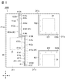
- FIG. 2A is a schematic plan view of the circuit module of the embodiment.
- 2B is a cross-sectional view taken along line AA in FIG. 2A.
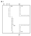
- FIG. 3 is a schematic plan view of a circuit board of the circuit module according to the embodiment.
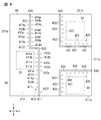
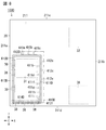
- FIG. 4 is a schematic plan view in which a part of the circuit module of the above embodiment is omitted.
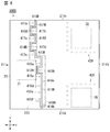
- FIG. 5 is a schematic plan view of a circuit module according to Modification 1 of the above embodiment.
- FIG. 6 is a schematic plan view of a circuit module according to Modification 2 of the above embodiment.
- FIG. 7 is a schematic plan view of a circuit module according to Modification 3 of the embodiment.
- FIG. 8 is a schematic plan view of a circuit module according to Modification 4 of the above embodiment.
- FIG. 9 is a schematic plan view of a circuit module according to Modification 5 of the above embodiment.
- FIG. 10 is a schematic plan view of a circuit module according to Modification 6 of the above embodiment.
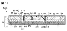
- FIG. 11 is a schematic cross-sectional view of a circuit module according to Modification 7 of the embodiment.
- FIG. 1 is a schematic circuit diagram of a circuit module 100 according to an embodiment of the present invention.
- the circuit module 100 is a circuit module used in a high frequency circuit.
- the circuit module 100 is a micro integrated module (front end module) in which various functional parts used in a wireless communication front end circuit (wireless front end circuit) are integrated.
- a front-end circuit is a circuit for transmitting a radio signal (transmission signal) received from an external device to an antenna and transmitting a radio signal (reception signal) received by the antenna to the external device.
- the circuit module 100 includes an input terminal 101, an output terminal 102, an antenna terminal 103, and a control terminal 104, as shown in FIG.
- the input terminal 101 is a terminal that is connected to an external device and receives a transmission signal from the external device.
- the output terminal 102 is connected to an external device and is a terminal for outputting a reception signal to the external device.
- the antenna terminal 103 is a terminal connected to an external antenna.
- the control terminal 104 is a terminal for receiving a control signal from an external device.
- the circuit module 100 includes various functional parts (electronic parts) used in a front-end circuit for wireless communication. As shown in FIG. 1, these electronic components include a power amplifier 31, a low noise amplifier 32, a plurality of duplexers 33, a first switch circuit 34, a second switch circuit 35, an antenna switch circuit 36, and a control. Circuit 37.
- these electronic components include a power amplifier 31, a low noise amplifier 32, a plurality of duplexers 33, a first switch circuit 34, a second switch circuit 35, an antenna switch circuit 36, and a control. Circuit 37.
- the power amplifier 31 is a circuit for amplifying a transmission signal sent from the external device to the antenna.
- the power amplifier 31 is, for example, a multiband power amplifier designed to operate in a plurality of communication bands.
- the power amplifier 31 has an input terminal electrically connected to the input terminal 101 and an output terminal electrically connected to the first switch circuit 34.
- the power amplifier 31 amplifies the transmission signal received from the input terminal 101 and outputs the amplified transmission signal to the first switch circuit 34.
- the low noise amplifier 32 is a circuit for amplifying a reception signal sent from an antenna to an external device.
- the low noise amplifier 32 has an input end electrically connected to the second switch circuit 35 and an output end electrically connected to the output terminal 102.
- the low noise amplifier 32 amplifies the reception signal received from the second switch circuit 35 and outputs the amplified reception signal to the output terminal 102.
- Each of the plurality of duplexers 33 includes a transmission side filter and a reception side filter.
- the transmission-side filter passes signals in the transmission frequency band and attenuates signals outside the transmission frequency band.
- the reception filter passes signals in the reception frequency band and attenuates signals outside the reception frequency band.
- the duplexer 33 has a function of filtering a signal in the transmission frequency band and a signal in the reception frequency band, and corresponds to a filter circuit.
- the plurality of duplexers 33 have different transmission frequency bands and reception frequency bands.
- the input terminal of the transmission filter is used as a transmission terminal that receives a transmission signal
- the output terminal of the reception filter is used as a reception terminal that outputs a reception signal.
- the connection point between the output terminal of the transmission filter and the input terminal of the reception filter is used as an antenna connection terminal for connection to the antenna.
- the first switch circuit 34, the second switch circuit 35, and the antenna switch circuit 36 are each a semiconductor switch circuit.
- the semiconductor switch circuit includes, for example, a field effect transistor (FET), a MEMS (Micro Electro Mechanical Systems) switch, or a bipolar transistor.
- the first switch circuit 34 includes a circuit that connects the output terminal of the power amplifier 31 to one of the transmission terminals of the plurality of duplexers 33.
- the duplexer 33 connected to the power amplifier 31 is selected from the plurality of duplexers 33 by switching the connection of the first switch circuit 34.
- the second switch circuit 35 includes a circuit that connects the input terminal of the low noise amplifier 32 to one of the reception terminals of the plurality of duplexers 33.
- the duplexer 33 connected to the low noise amplifier 32 can be selected from a plurality of duplexers 33 by switching the connection of the second switch circuit 35.
- the antenna switch circuit 36 includes a circuit that connects the antenna terminal 103 to one of the antenna connection terminals of the plurality of duplexers 33. That is, the antenna switch circuit 36 is a circuit for selecting the duplexer 33 connected to the antenna terminal 103 from the plurality of duplexers 33.
- a plurality of duplexers 33 may be selected at the same time.
- the control circuit 37 receives a control signal from an external device via the control terminal 104, and controls each of the first switch circuit 34, the second switch circuit 35, and the antenna switch circuit 36 based on the control signal.
- the control circuit 37 connects the power amplifier 31, the low noise amplifier 32, and the antenna terminal 103 to a specific duplexer 33 among the plurality of duplexers 33. That is, the duplexer 33 suitable for the transmission signal and the reception signal is selected as the specific duplexer 33.
- the control circuit 37 is, for example, an integrated circuit.
- FIG. 2A, FIG. 2B, FIG. 3, and FIG. 4 the components of the circuit module 100 are schematically shown for easy understanding of the structure of the circuit module 100.
- 2A and 4 are both schematic plan views of the circuit module 100.
- some of the electronic components 30 are not shown in order to explain the structure of the circuit module 100 in more detail. Yes.
- the expression “in a plan view” has the same meaning as “when the circuit module 100 is viewed from the thickness direction”.
- the circuit module 100 includes a circuit board 20, a plurality of electronic components 30, a plurality of conductor posts 40, a mold layer 50, and a shield layer 60, as shown in FIGS. 2A and 2B.
- the circuit board 20 is a quadrangular multilayer substrate (resin multilayer substrate or ceramic multilayer substrate) as shown in FIGS. 2A, 2B, and 3.
- the circuit board 20 includes an electrical insulation layer (first electrical insulation layer) 21, a ground layer (first ground layer) 22, an electrical insulation layer (second electrical insulation layer) 23, and a ground layer (second ground layer). 24.
- the first electrical insulating layer 21 has a mounting surface (upper surface in FIG. 2B) 211.
- the mounting surface 211 is a substantially flat surface with micro level unevenness, and a plurality of electronic components 30 are mounted thereon.
- the first ground layer 22 is on the side opposite to the mounting surface 211 in the first electrical insulating layer 21 (the lower side in FIG. 2B).
- the first ground layer 22 is formed so as to cover the entire surface of the first electrical insulating layer 21 opposite to the mounting surface 211 (the lower surface of the circuit module 100 in FIG. 2B).
- the first ground layer 22 has three gaps (first gap, second gap, and third gap) 221, 222, and 223 as shown in FIG.
- the first gap 221 is formed so as to face a slit 610 (see FIG. 2A) described later. In other words, the first gap 221 extends along the slit 610.
- the second gap 222 is formed so as to face a slit 620 (see FIG. 2A) described later.
- the second gap 222 extends along the slit 620.
- the third gap 223 is formed so as to face a slit 630 (see FIG. 2A) described later. In other words, the third gap 223 extends along the slit 630. Therefore, in the first ground layer 22, noise propagation across the gaps 221, 222, and 223 is suppressed.
- the second electrical insulation layer 23 is on the opposite side of the first ground layer 22 from the first electrical insulation layer 21 (lower side in FIG. 2B).
- the second electrical insulating layer 23 is formed so as to cover the entire surface of the first ground layer 22 opposite to the first electrical insulating layer 21 (the lower surface of the circuit module 100 in FIG. 2B). Since the first ground layer 22 has the three gaps 221, 222, and 223 as described above, the first electrical insulating layer 21 and the second electrical insulating layer 23 are located inside the gaps 221, 222, and 223, respectively. Then it is united.
- the second ground layer 24 is on the opposite side of the second electrical insulating layer 23 from the first ground layer 22 (lower side in FIG. 2B).
- the second ground layer 24 is formed so as to cover the entire surface of the second electrical insulating layer 23 opposite to the first ground layer 22 (the lower surface of the circuit module 100 in FIG. 2B).
- the surface of the second ground layer 24 opposite to the second electrical insulating layer 23 is the bottom surface of the circuit board 20.
- the first electrical insulating layer 21 has a plurality of vias (through conductors) 212 for electrically connecting the plurality of conductor posts 40 to the first ground layer 22.
- the second electrical insulating layer 23 has a plurality of vias (penetrating conductors) 231 for electrically connecting the first ground layer 22 and the second ground layer 24. That is, each conductor post 40 is electrically connected to the first ground layer 22 via the via 212 and further electrically connected to the second ground layer 24 by a plurality of vias (penetrating conductors) 231. .
- the plurality of electronic components 30 include a power amplifier 31, a low noise amplifier 32, a plurality of duplexers 33, a first switch circuit 34, a second switch circuit 35, an antenna switch circuit 36, and a control circuit 37. . Further, as shown in FIG. 2A, the plurality of electronic components 30 include a plurality of capacitors 38 and a plurality of inductors 39.
- the power amplifier 31 is an electronic component (first electronic component) serving as a noise generation source.
- the frequency of noise generated by the power amplifier 31 depends on the frequency band of the transmission signal amplified by the power amplifier 31.
- the noise frequency is about several hundred MHz to several GHz.
- the low noise amplifier 32 and the antenna switch circuit 36 are electronic components (second electronic components) that are to be protected from noise generated in the power amplifier 31 (first electronic component).
- the power amplifier 31 is mounted on the first end (left end in FIG. 2A) 211a side of the mounting surface 211 in the first direction X.
- the low noise amplifier 32 and the antenna switch circuit 36 are mounted on the second end (right end in FIG.
- the low noise amplifier 32 and the antenna switch circuit 36 include a first end (upper end in FIG. 2A) 211c side and a second end (lower end in FIG. 2A) 211d in the second direction Y orthogonal to the first direction X of the mounting surface 211. Each is implemented on the side.
- the first switch circuit 34 and the second switch circuit 35 are mounted on the first end 211 c side in the second direction Y in the vicinity of the center of the mounting surface 211 in the first direction X.
- the control circuit 37 is mounted on the mounting surface 211 between the power amplifier 31 and the second end 211 d of the mounting surface 211 in the second direction Y.
- the plurality of capacitors 38 and the plurality of inductors 39 are appropriately mounted on the mounting surface 211.
- the plurality of conductor posts 40 are provided to electromagnetically shield between the first electronic component that is a noise generation source and the second electronic component that is a protection target from noise generated in the first electronic component. By providing the plurality of conductor posts 40, it is possible to improve the isolation characteristics between the electronic components (between the first electronic component and the second electronic component).
- the plurality of conductor posts 40 include three groups 400 (first group 410, second group 420, and third group 430) of conductor posts 40, as shown in FIGS. 2A and 4.
- the conductor posts 40 included in the first group 410 are referred to as conductor posts 41 as necessary.
- each conductor post 40 is formed of a conductive material.
- the conductive material is, for example, a metal such as aluminum, copper, or iron, or a resin such as an elastomer mixed with a conductive material.
- the shape of each conductor post 40 is, for example, a cylindrical shape. All of the plurality of conductor posts 40 are electrically connected to the first ground layer 22 by vias 212.
- the interval between the conductor posts 40 in the group 400 of conductor posts 40 may be 1/16 or less of the wavelength of noise generated in the power amplifier 31 that is the first electronic component. In this way, the possibility of noise passing through the gap between the conductor posts 40 can be more effectively reduced.
- Such a conductor post 40 can be arranged using a vacant area on the mounting surface 211 where the electronic component 30 is not mounted. That is, the conductor post 40 can be arranged without changing the arrangement of the electronic component 30.
- the lower limit value of the interval between the conductor posts 40 is not particularly limited, and may be set as appropriate according to a desired noise reduction level.
- the first group 410 is a group of a plurality of conductor posts 41 arranged so as to cross between the power amplifier 31, the low noise amplifier 32, and the antenna switch circuit 36 on the mounting surface 211.
- the plurality of conductor posts 41 are provided to protect the second electronic component (in the present embodiment, the low noise amplifier 32 and the antenna switch circuit 36) from noise generated in the first electronic component (power amplifier 31). More specifically, as shown in FIG. 4, the plurality of conductor posts 41 are arranged so as to cross the mounting surface 211 in the second direction Y. Thus, the plurality of conductor posts 41 can electromagnetically shield the region of the mounting surface 211 where the power amplifier 31 exists and the region of the mounting surface 211 where the low noise amplifier 32 and the antenna switch circuit 36 exist.
- the plurality of conductor posts 41 include a plurality of conductor posts 411a, 411b, 411c, 411d, 411e, 411f, 411g, 411h, 411i, and a plurality of conductor posts 412a, 412b, 412c, 412d, 412e. , 412f.
- the plurality of conductor posts 41 include a plurality of conductor posts 413a, 413b, 413c, 413d, 413e, 413f, and a plurality of conductor posts 414a, 414b, 414c, 414d, 414e, 414f, 414g, 414h.
- the plurality of conductor posts 411a to 411i are provided from the first end 211c in the second direction Y to the second end 211d between the low noise amplifier 32 and the antenna switch circuit 36 in the first direction X of the mounting surface 211 and the power amplifier 31.
- the plurality of conductor posts 411a to 411d are opposed to the power amplifier 31 in the first direction X. That is, the plurality of conductor posts 411a to 411d may be disposed adjacent to the power amplifier 31. In other words, there is no electronic component 30 different from the power amplifier 31 between the conductor posts 411a to 411d and the power amplifier 31.
- the plurality of conductor posts 412a to 412f are arranged between the low noise amplifier 32 and the antenna switch circuit 36 in the first direction X and the group of the plurality of conductor posts 411a to 411i from the first end 211c toward the second end 211d. It is arranged in a line along the two directions Y.
- the conductor posts 412a to 412e face the conductor posts 411a to 411e in the first direction X. The reason why the interval between the conductor posts 412e and 412f is larger than the interval between the conductor posts 412a to 412e is that the duplexer 33 is avoided (see FIG. 2A).
- the plurality of conductor posts 413 a to 413 f are arranged in a line along the second direction Y between the first end 211 c of the mounting surface 211 in the second direction Y and the power amplifier 31.
- the plurality of conductor posts 414 a to 414 h are arranged in a line along the second direction Y between the first end 211 c in the second direction Y of the mounting surface 211 and the power amplifier 31.
- the plurality of conductor posts 414a to 414h are closer to the low noise amplifier 32 than the plurality of conductor posts 413a to 413f.
- the conductor posts 413a to 413f and the conductor posts 414a to 414h are located between the power amplifier 31 and the low noise amplifier 32 in a direction connecting the center of the power amplifier 31 and the center of the low noise amplifier 32.
- the conductor posts 413a to 413f face the conductor posts 414c to 414h in the first direction X, respectively.
- the second group 420 is a group of a plurality of conductor posts 42 arranged so as to cross between the power amplifier 31 and the low noise amplifier 32 on the mounting surface 211.
- the plurality of conductor posts 42 are provided to protect the second electronic component (low noise amplifier 32) from noise generated in the first electronic component (power amplifier 31).
- the group of the plurality of conductor posts 42 included in the second group 420 is disposed between the first group 410 and the low noise amplifier 32 on the mounting surface 211. More specifically, as shown in FIG. 4, the plurality of conductor posts 42 are arranged in an L shape so as to partially surround the low noise amplifier 32.
- the second group 420 includes a plurality (six in FIG.
- the plurality of conductor posts 421 are arranged in a line along the first direction X between the power amplifier 31 and the low noise amplifier 32 in the second direction Y of the mounting surface 211. Part of the plurality of conductor posts 421 faces the low noise amplifier 32 in the second direction Y.
- the plurality of conductor posts 422 are arranged in a line along the second direction Y between the power amplifier 31 and the low noise amplifier 32 in the first direction X of the mounting surface 211. A part of the plurality of conductor posts 422 faces the low noise amplifier 32 in the first direction X.
- Each conductor post 42 is disposed adjacent to the low noise amplifier 32. In other words, there is no electronic component 30 different from the low noise amplifier 32 between the conductor post 42 and the low noise amplifier 32. 2A and 4, the number of conductor posts 42 is 13, but is not particularly limited.
- the third group 430 is a group of a plurality of conductor posts 43 arranged so as to cross between the power amplifier 31 and the antenna switch circuit 36 on the mounting surface 211 as shown in FIG. 2A.
- the plurality of conductor posts 43 are provided to protect the second electronic component (antenna switch circuit 36) from noise generated in the first electronic component (power amplifier 31).
- the group of the plurality of conductor posts 43 included in the third group 430 is disposed between the first group 410 and the antenna switch circuit 36 on the mounting surface 211. More specifically, as shown in FIG. 4, the plurality of conductor posts 43 are arranged in an L shape so as to partially surround the antenna switch circuit 36.
- the third group 430 includes a plurality (six in FIG.
- conductor posts 431 and a plurality (five in FIG. 4) conductor posts 432 are arranged in a line along the second direction Y between the power amplifier 31 and the antenna switch circuit 36 in the first direction X of the mounting surface 211. Part of the plurality of conductor posts 431 faces the antenna switch circuit 36 in the first direction X.
- the plurality of conductor posts 432 are arranged in a line along the first direction X between the power amplifier 31 and the antenna switch circuit 36 in the second direction Y of the mounting surface 211. A part of the plurality of conductor posts 432 faces the antenna switch circuit 36 in the second direction Y.
- Each conductor post 43 is disposed adjacent to the antenna switch circuit 36. In other words, there is no electronic component 30 different from the antenna switch circuit 36 between the conductor post 43 and the antenna switch circuit 36. 2A and 4, the number of conductor posts 43 is 11, but is not particularly limited.
- the plurality of conductor posts 40 includes a group of conductor posts 41 (first group) 410, a group of conductor posts 42 (second group) 420, and a group of conductor posts 43 (third group). ) 3 groups with 430.
- the first group 410 is closer to the first electronic component (power amplifier 31) than the second group 420 and the third group 430.
- the plurality of conductor posts 40 include a plurality of groups, the group of conductor posts including the conductor posts 40 closest to the first electronic component is referred to as a main conductor post group (or a group of first conductor posts).
- a group of conductor posts 40 other than the group of posts is called a group of sub conductor posts.
- the group of sub-conductor posts (or the group of second conductor posts) is a conductor post disposed between the group of main conductor posts and the second electronic component on the mounting surface 211 and electrically connected to the ground layer. Defined as a group.
- the mold layer 50 is formed on the mounting surface 211 as shown in FIG. 2B.
- the mold layer 50 is electrically insulating and seals the plurality of electronic components 30 and the plurality of conductor posts 40.
- the mold layer 50 is formed so as to cover the entire mounting surface 211.
- the mold layer 50 is formed of an electrically insulating resin (for example, an epoxy resin).
- the mold layer 50 is formed so that the surface (the upper surface in FIG. 2B) 501 opposite to the mounting surface 211 is flat.
- the mold layer 50 is formed such that the tips of the plurality of conductor posts 40 are exposed on the surface 501.
- the shield layer 60 is provided in order to suppress noise emission from the inside of the circuit module 100 to the outside and noise intrusion from the outside to the inside of the circuit module 100.
- the shield layer 60 is formed on the surface 501 of the mold layer 50 opposite to the mounting surface 211.
- the shield layer 60 covers the entire surface 501 of the mold layer 50.
- the shield layer 60 is formed on the surface 501 so as to contact the tips of the plurality of conductor posts 40. Therefore, the shield layer 60 is electrically connected to the second ground layer 24 via the plurality of conductor posts 40, the plurality of vias 212, and the first ground layer 22.
- the shield layer 60 is electrically connected to the ground layer 22 by the plurality of conductor posts 40, there is no need to newly provide a grounding wiring for the shield layer 60.
- the shield layer 60 has three slits 600 (a slit 610, a slit 620, and a slit 630) as shown in FIGS. 2A and 4.
- Each slit 600 has a space between the conductor post 40 and the first electronic component or between the conductor post 40 and the second electronic component in a plan view with respect to each conductor post 40 included in the group 400 of conductor posts 40. Stretch through.
- the space between the conductor post 40 and the first electronic component is perpendicular to the straight line connecting the first electronic component and the second electronic component and passes through the conductor post 40 and the first straight line perpendicular to the straight line. It means between the center line passing through the electronic component.
- the space between the conductor post 40 and the second electronic component is perpendicular to the straight line connecting the first electronic component and the second electronic component and passes through the conductor post 40 and the second electron perpendicular to the straight line. It means between the center line passing through the part.
- the shield layer 60 is formed of a conductive material.
- the conductive material is, for example, a metal such as aluminum, copper, or iron, or a resin such as an elastomer mixed with a conductive material.
- the shield layer 60 can be formed by a known thin film forming technique such as sputtering.
- the slit 600 is formed by partially removing the shield layer 60 using a dicer or a laser. That is, the slit 600 can be formed only by processing the shield layer 60, and there is no need to process the mold layer 50. Therefore, the manufacturing cost can be reduced.
- the slit 610 is formed along the first group 410. That is, the slit 610 corresponds to the first group 410.
- the slit 610 crosses between the power amplifier 31, the low noise amplifier 32, and the antenna switch circuit 36. More specifically, as shown in FIG. 4, the slit 610 has a Z shape that crosses the shield layer 60 in the second direction Y.
- the slit 610 has a first part 611, a second part 612, and a third part 613.
- the first portion 611 is a straight line extending along the second direction Y of the mounting surface 211, and passes between the set of conductor posts 411a to 411i and the set of conductor posts 412a to 412f.
- the first portion 611 is located between the conductor post 41 and the antenna switch circuit 36 in plan view with respect to the conductor post 41 (411a to 411i) of the first group 410 (that is, the antenna switch with respect to the conductor post 41). Circuit 36 side).
- the first portion 611 is located between the conductor post 41 and the power amplifier 31 in plan view with respect to the conductor posts 41 (412a to 412f) of the first group 410 (that is, the power amplifier 31 with respect to the conductor posts 41).
- Side The second portion 612 has a linear shape extending along the second direction Y of the mounting surface 211, and passes between the set of conductor posts 413a to 413f and the set of conductor posts 414a to 414h.
- the second portion 612 is between the conductor post 41 and the low noise amplifier 32 in plan view with respect to the conductor posts 41 (413a to 413f) of the first group 410 (that is, the low noise amplifier 32 with respect to the conductor posts 41). Side). Further, the second portion 612 is located between the conductor post 41 and the power amplifier 31 in a plan view with respect to the conductor posts 41 (414a to 414h) of the first group 410 (that is, the power amplifier 31 with respect to the conductor posts 41). Side).
- the third part 613 connects the first part 611 and the second part 612.
- the slit 610 crosses between the first electronic component (power amplifier 31) and the second electronic component (low noise amplifier 32 and antenna switch circuit 36) along the group of conductor posts 410. Moreover, both ends of the slit 610 are open. That is, in the shield layer 60, the portion covering the surface 501 of the mold layer 50 is divided by the slit 610.
- the slit 620 is formed along the second group 420. That is, the slit 620 corresponds to the second group 420.
- the slit 620 crosses between the power amplifier 31 and the low noise amplifier 32. More specifically, as shown in FIG. 4, the slit 620 has an L shape that partially surrounds the low noise amplifier 32.
- the slit 620 has a first part 621 and a second part 622.
- the first portion 621 is a straight line extending along the first direction X of the mounting surface 211, and the conductor post 421 and the first electronic component (power amplifier) in plan view with respect to the conductor posts 421 of the second group 420. 31) (that is, the first electronic component side with respect to the conductor post 421).
- the second portion 622 is a straight line extending along the second direction Y of the mounting surface 211, and the conductor post 422 and the first electronic component (power amplifier) in plan view with respect to the conductor posts 422 of the second group 420. 31) (that is, the first electronic component side with respect to the conductor post 422).
- the slit 620 crosses between the first electronic component (power amplifier 31) and the second electronic component (low noise amplifier 32) along the conductor post group 420.
- both ends of the slit 620 are open. That is, in the shield layer 60, a portion covering the surface 501 of the mold layer 50 is divided by the slit 620.
- the slit 630 is formed along the third group 430. That is, the slit 630 corresponds to the third group 430.
- the slit 630 crosses between the power amplifier 31 and the antenna switch circuit 36. More specifically, as shown in FIG. 4, the slit 630 has an L shape that partially surrounds the antenna switch circuit 36.
- the slit 630 has a first part 631 and a second part 632.
- the first portion 631 is a straight line extending along the second direction Y of the mounting surface 211, and the conductor post 431 and the first electronic component (power amplifier) in the plan view with respect to the conductor posts 431 of the third group 430. 31) (that is, the first electronic component side with respect to the conductor post 431).
- the second portion 632 is a straight line extending along the first direction X of the mounting surface 211, and the conductor post 432 and the first electronic component (power amplifier) in plan view with respect to the conductor posts 432 of the third group 430. 31) (that is, the first electronic component side with respect to the conductor post 432).
- the slit 630 crosses between the first electronic component (power amplifier 31) and the second electronic component (antenna switch circuit 36) along the conductor post group 430.
- both ends of the slit 630 are open. That is, in the shield layer 60, a portion covering the surface 501 of the mold layer 50 is divided by the slit 630.
- the shield layer 60 includes three slits 600 including a slit 610, a slit 620, and a slit 630.
- the slit 610 corresponding to the first group 410 that is a group of first conductor posts is referred to as a first slit (or main slit)
- the second group 420 and the third group that are groups of second conductor posts.
- the slits 620 and the slits 630 respectively corresponding to the group 430 are referred to as second slits (or sub slits).
- the second slit is, in plan view, between each second conductor post and the first conductor post group, or between the second conductor post and the second conductor post, with respect to each second conductor post included in the second conductor post group. It is defined as a slit that passes between two electronic components.
- the shield layer 60 has a slit 610 that crosses between the power amplifier 31, the low noise amplifier 32, and the antenna switch circuit 36.
- the slit 610 exists between the part covering the power amplifier 31 and the part covering the low noise amplifier 32 and the antenna switch circuit 36 in the shield layer 60. Therefore, the noise generated in the power amplifier 31 is prevented from entering the low noise amplifier 32 and the antenna switch circuit 36 via the shield layer 60.
- both ends of the slit 610 are open, the portion covering the power amplifier 31 in the shield layer 60 is separated from the portion covering the low noise amplifier 32 and the antenna switch circuit 36.
- the slit 610 is formed in the shield layer 60, noise generated in the power amplifier 31 may be radiated to the outside of the circuit module 100 through the slit 610.
- the slits 610 are formed on the conductor posts 41 (411a to 411i, 413a to 413f) included in the first group 420 in the plan view and the second electronic components (low noise amplifier 32 and antenna switch circuit 36). ). In other words, the slit 610 passes through the opposite side of the conductor post 41 from the power amplifier 31 in plan view with respect to each conductor post 41 (411a to 411i, 413a to 413f) included in the first group 420.
- the group 410 of the conductor posts 41 suppresses noise emission to the outside. Therefore, radiation of noise from the power amplifier 31 to the outside can be suppressed.
- the slit 610 crosses between the power amplifier 31, the low noise amplifier 32, and the antenna switch circuit 36 along the group of conductor posts 410. That is, the slit 610 is closer to the conductor post group 410 than the power amplifier 31, the low noise amplifier 32, and the antenna switch circuit 36. Thus, the closer the slit 610 is to the conductor post group 410, the higher the effect of suppressing noise emission to the outside and noise intrusion from the outside.
- the first gap 221 of the first ground layer 22 extends along the slit 610. Therefore, the first gap 221 is between the first electronic component (power amplifier 31) and the second electronic component (low noise amplifier 32 and antenna switch circuit 36) along the conductor post group 410, like the slit 610. Across. That is, the first gap 221 exists between the part corresponding to the power amplifier 31 and the part corresponding to the low noise amplifier 32 and the antenna switch circuit 36 in the first ground layer 22. Therefore, noise generated in the power amplifier 31 is prevented from entering the low noise amplifier 32 and the antenna switch circuit 36 via the first ground layer 22.
- the shield layer 60 has a slit 620 that crosses between the power amplifier 31 and the low noise amplifier 32. That is, the slit 620 exists between the part covering the power amplifier 31 and the part covering the low noise amplifier 32 in the shield layer 60. Therefore, noise generated in the power amplifier 31 is prevented from entering the low noise amplifier 32 via the shield layer 60.
- the portion covering the power amplifier 31 in the shield layer 60 is separated from the portion covering the low noise amplifier 32. This further suppresses noise generated in the power amplifier 31 from entering the low noise amplifier 32 through the shield layer 60.
- the slit 620 is formed in the shield layer 60, noise may enter the circuit module 100 through the slit 620 and reach the low noise amplifier 32.
- the slit 620 is provided between the conductor post 42 and the power amplifier 31 in plan view with respect to each conductor post 42 included in the second group 420 (that is, on the opposite side of the conductor post 42 from the low noise amplifier 32). Pass through.
- noise that has entered the circuit module 100 through the slit 620 flows to the first ground layer 22 by the conductor posts 42 of the second group 420. That is, the group 420 of the conductor posts 42 suppresses intrusion of noise from the outside. Therefore, the low noise amplifier 32 can be protected from noise.
- the slit 620 crosses between the power amplifier 31 and the low noise amplifier 32 along the group of conductor posts 420. That is, the slit 620 is closer to the conductor post group 420 than the power amplifier 31 and the low noise amplifier 32.
- the closer the slit 620 is to the conductor post group 420 the higher the effect of suppressing noise emission to the outside and noise intrusion from the outside.
- the second gap 222 of the first ground layer 22 extends along the slit 620. Accordingly, the second gap 222 crosses between the first electronic component (power amplifier 31) and the second electronic component (low noise amplifier 32) along the conductor post group 420, like the slit 620. That is, the second gap 222 exists between the portion corresponding to the power amplifier 31 and the portion corresponding to the low noise amplifier 32 in the first ground layer 22. Therefore, noise generated in the power amplifier 31 is suppressed from entering the low noise amplifier 32 via the first ground layer 22.
- the shield layer 60 has a slit 630 that crosses between the power amplifier 31 and the antenna switch circuit 36. That is, the slit 630 exists between the part covering the power amplifier 31 and the part covering the antenna switch circuit 36 in the shield layer 60. Therefore, noise generated in the power amplifier 31 is suppressed from entering the antenna switch circuit 36 via the shield layer 60. In particular, in the present embodiment, since both ends of the slit 630 are open, the portion covering the power amplifier 31 in the shield layer 60 is separated from the portion covering the antenna switch circuit 36. This further suppresses noise generated in the power amplifier 31 from entering the antenna switch circuit 36 via the shield layer 60. If the slit 630 is formed in the shield layer 60, noise may enter the circuit module 100 through the slit 630 and reach the antenna switch circuit 36. However, the slit 630 is between the conductor post 43 and the power amplifier 31 in plan view with respect to each conductor post 43 included in the third group 430 (that is, on the side opposite to the antenna switch circuit 36 in the conductor post 43). Pass through.
- the slit 630 crosses between the power amplifier 31 and the antenna switch circuit 36 along the group of conductor posts 430. That is, the slit 630 is closer to the conductor post group 430 than the power amplifier 31 and the antenna switch circuit 36.
- the closer the slit 630 is to the group of conductor posts 430 the higher the effect of suppressing external noise emission and noise entry from the outside.
- the third gap 223 of the first ground layer 22 extends along the slit 630. Accordingly, the third gap 223 crosses between the first electronic component (power amplifier 31) and the second electronic component (antenna switch circuit 36) along the conductor post group 430, similarly to the slit 630. That is, the third gap 223 exists between the portion corresponding to the power amplifier 31 and the portion corresponding to the antenna switch circuit 36 in the first ground layer 22. Therefore, noise generated in the power amplifier 31 is prevented from entering the antenna switch circuit 36 via the first ground layer 22.
- the plurality of conductor posts 40 include a second group 420 and a third group 430 that are sub-conductor post groups in addition to the first group 410 that is a main conductor post group. Including. Therefore, the isolation characteristics between the first electronic component and the second electronic component can be further improved as compared with the case where the plurality of conductor posts 40 include only the group of main conductor posts.
- the shield layer 60 includes a slit 620 and a slit 630 that become the second slit in addition to the slit 610 that becomes the first slit. Therefore, compared with the case where the shield layer 60 includes only the first slit, the noise wraparound by the shield layer 60 can be further suppressed.
- the plurality of conductor posts 40 include the conductor post group 400 (410, 420, 430).
- the conductor post group 400 (410, 420, 430) is arranged on the mounting surface 211 so as to cross between the first electronic component (power amplifier 31) and the second electronic component (low noise amplifier 32, antenna switch circuit 36). And electrically connected to the ground layer 22. Therefore, the isolation characteristic between the first electronic component and the second electronic component can be improved.
- the shield layer 60 has slits 600 (610, 620, 630).
- the slit 600 is formed between the conductor post 40 and the first electronic component (power amplifier 31) or between the conductor post 40 and the second electronic component (in the plan view) with respect to each conductor post 40 included in the group 400 of conductor posts. It extends between the low noise amplifier 32 and the antenna switch circuit 36). That is, the slit 600 crosses between the first electronic component (power amplifier 31) and the second electronic component (low noise amplifier 32, antenna switch circuit 36) along the conductor post group 400. Therefore, noise wraparound by the shield layer 60 can be reduced.
- the group of conductor posts (410, 420, 430) suppresses radiation of noise to the outside and intrusion of noise from the outside through the slits (610, 620, 630). Therefore, according to the circuit module 100 of the present embodiment, noise wraparound by the shield layer 60 is reduced while suppressing noise emission to the outside and noise intrusion from the outside, and isolation characteristics between electronic components are reduced. Can be improved.
- FIG. 5 shows a circuit module 100A according to a first modification.
- the plurality of conductor posts 40 include a first group 410A, a second group 420A, and a third group 430A.
- the first group 410A is a group of conductor posts 41 arranged so as to cross between the power amplifier 31, the low noise amplifier 32, and the antenna switch circuit 36 on the mounting surface 211.
- the number of conductor posts 41 is smaller than that of the first group 410.
- the conductor posts 41 of the first group 410A include a plurality of conductor posts 411b, 411d, 411f, 411g, 411h, 411i and a plurality of conductor posts 412a, 412c, 412e, 412f. Further, the conductor post 41 of the first group 410A includes a plurality of conductor posts 413a, 413c, 413e and a plurality of conductor posts 414a, 414b, 414d, 414f, 414h. In the first group 410A, the conductor posts 41 are arranged so as not to face each other in the first direction X of the mounting surface 211.
- the second group 420A is a group of a plurality of conductor posts 42 arranged so as to cross between the power amplifier 31 and the low noise amplifier 32 on the mounting surface 211.
- the second group 420 includes a plurality (three in FIG. 5) conductor posts 421 and a plurality (four in FIG. 5) conductor posts 422. That is, the second group 420A has fewer conductor posts 42 (421, 422) than the second group 420.
- the interval between the conductor posts 42 is set to 1/16 or less of the wavelength of noise generated in the power amplifier 31.
- the third group 430A is a group of a plurality of conductor posts 43 arranged so as to cross between the power amplifier 31 and the antenna switch circuit 36 on the mounting surface 211.
- the third group 430 includes a plurality of (three in FIG. 5) conductor posts 431 and a plurality (three in FIG. 5) conductor posts 432. That is, the third group 430A has fewer conductor posts 43 (431, 432) than the third group 430. However, the interval between the conductor posts 43 is set to 1/16 or less of the wavelength of noise generated in the power amplifier 31.
- the shield layer 60 has a slit 610A, a slit 620A, and a slit 630A.
- the slit 610A has a first part 611, a second part 612, and a third part 613.
- both ends of the slit 610A are not open. That is, the shield layer 60 is not divided by the slit 610 ⁇ / b> A at the portion covering the surface 501 of the mold layer 50.
- the slit 620A has a first portion 621 and a second portion 622. However, both ends of the slit 620A are not open.
- the shield layer 60 is not divided by the slit 620 ⁇ / b> A at the portion covering the surface 501 of the mold layer 50.
- the slit 630A has a first portion 631 and a second portion 632. However, both ends of the slit 630A are not open. That is, the shield layer 60 is not divided by the slit 630 ⁇ / b> A at the portion covering the surface 501 of the mold layer 50.
- the noise wraparound by the shield layer 60 is reduced, and between the electronic components is reduced. Isolation characteristics can be improved. Further, if the distance between the conductor posts 40 (41, 42, 43) is 1/16 or less of the wavelength of noise generated in the power amplifier 31, the effect of the conductor post group 400 can be maintained. That is, it is possible to maintain the effect of suppressing external noise emission and external noise intrusion. Therefore, in the circuit module 100A, it is possible to reduce the number of the conductor posts 40 while maintaining the effect of suppressing the radiation of noise to the outside and the intrusion of noise from the outside. The area required for installation can be reduced.
- FIG. 6 shows a circuit module 100B according to a second modification.
- the plurality of conductor posts 40 include a first group 410B, a second group 420, and a third group 430.
- the first group 410B is a group of a plurality of conductor posts 41 arranged so as to cross between the power amplifier 31, the low noise amplifier 32, and the antenna switch circuit 36 on the mounting surface 211.
- the plurality of conductor posts 41 include a plurality (six in FIG. 6) of conductor posts 415a, 415b, 415c, 415d, 415e, and 415f and a plurality (two in FIG. 6) of conductor posts 416a and 416b.
- the plurality of conductor posts 41 further include a plurality (five in FIG. 6) of conductor posts 417a, 417b, 417c, 417d, and 417e.
- the plurality of conductor posts 415a to 415f are provided between the low-noise amplifier 32 and the antenna switch circuit 36 and the power amplifier 31 in the first direction X of the mounting surface 211 from the first end 211c in the second direction Y to the second end 211d. In a row along the second direction Y.
- the plurality of conductor posts 415a to 415c are opposed to the power amplifier 31 in the first direction X. That is, the plurality of conductor posts 415 a to 415 c are disposed adjacent to the power amplifier 31. In other words, there is no electronic component 30 different from the power amplifier 31 between the conductor posts 415a to 415c and the power amplifier 31.
- the plurality of conductor posts 416a and 416b are arranged in the second direction from the first end 211c toward the second end 211d between the low noise amplifier 32 and the antenna switch circuit 36 and the group of conductor posts 415a to 415f in the first direction X. Line up along Y.
- the conductor post 416a is located between the conductor posts 415c and 415d in the second direction Y.
- the conductor post 416b is located between the conductor post 415f and the second end 211d in the second direction Y.
- the plurality of conductor posts 417 a to 417 e are arranged in a line along the second direction Y between the first end 211 c in the second direction Y of the mounting surface 211 and the power amplifier 31.
- the interval between two adjacent conductor posts is set to 1/16 or less of the wavelength of noise generated in the power amplifier 31.
- the shield layer 60 has the slit 610B, but does not have the slit 620 and the slit 630.
- the shield layer 60 has the first slit but does not have the second slit.
- the slit 610B is formed along the first group 410B. That is, the slit 610B corresponds to the first group 410B.
- the slit 610 ⁇ / b> B crosses between the power amplifier 31, the low noise amplifier 32, and the antenna switch circuit 36.
- the slit 610B includes a first part 611B, a second part 612B, a third part 613B, a fourth part 614B, a fifth part 615B, a sixth part 616B, and a seventh part 617B.
- a first part 611B a first part 611B, a second part 612B, a third part 613B, a fourth part 614B, a fifth part 615B, a sixth part 616B, and a seventh part 617B.
- the first portion 611B extends from the second end 211d in the second direction Y of the mounting surface 211 through between the set of conductor posts 415c to 415f and the set of conductor posts 416a and 416b. That is, the first portion 611B passes between the conductor post 41 and the antenna switch circuit 36 with respect to the conductor posts 41 (415c to 415f) of the first group 410B. The first portion 611B passes between the conductor post 41 and the power amplifier 31 with respect to the conductor post 41 (416a, 416b) of the first group 410B.
- the second portion 612B extends from the first portion 611B through between the conductor post 415b and the power amplifier 31.
- the third portion 613B extends from the second portion 612B between the conductor post 415a and the low noise amplifier 32 and the antenna switch circuit 36, and between the conductor post 417e and the low noise amplifier 32.
- the fourth portion 614B extends from the third portion 613B between the conductor post 417d and the power amplifier 31.
- the fifth portion 615B extends from the fourth portion 614B through between the conductor post 415a and the low noise amplifier 32.
- the sixth portion 616B extends from the fifth portion 615B through between the conductor post 417d and the power amplifier 31.
- the seventh portion 617B extends from the sixth portion 616B through between the conductor post 415a and the low noise amplifier 32.
- the slit 610B passes through between one of the two adjacent conductor posts 41 and the first electronic component (power amplifier 31) and between the other and the second electronic component (antenna switch circuit 36). (611B to 613B).
- the slit 610B passes through between one of the two adjacent conductor posts 41 and the first electronic component (power amplifier 31) and between the other and the second electronic component (low noise amplifier 32) (613B to 613B). 617B).
- the two conductor posts 41 adjacent to both sides of the slit 610B are provided. Will be located.
- the same effect as that obtained when the set of conductor posts 413a to 413f and the set of conductor posts 414a to 414h are arranged on both sides of the slit 610 can be obtained. That is, the number of the conductor posts 40 (41) can be reduced while maintaining the effect of suppressing the radiation of noise to the outside and the intrusion of noise from the outside, thereby reducing the manufacturing cost and the conductor posts 40 (41). The area required for installation can be reduced.
- FIG. 7 shows a circuit module 100C according to a third modification.
- the plurality of conductor posts 40 include the first group 410C, but do not include the second group 420 and the third group 430.
- the first group 410C is a group of a plurality of conductor posts 41 arranged so as to cross between the power amplifier 31, the low noise amplifier 32, and the antenna switch circuit 36 on the mounting surface 211.
- the plurality of conductor posts 41 include a plurality (six in FIG. 6) of conductor posts 415a, 415b, 415c, 415d, 415e, and 415f and a plurality (two in FIG. 6) of conductor posts 416a and 416b.
- the plurality of conductor posts 41 further include a plurality (six in FIG. 6) of conductor posts 418a, 418b, 418c, 418d, 418e, and 418f.
- the plurality of conductor posts 418 a to 418 f are arranged along the second direction Y between the first end 211 c in the second direction Y of the mounting surface 211 and the power amplifier 31.
- the conductor posts 418a to 418e are arranged in a line.
- the conductor posts 418a and 418b are located on both sides of the capacitor 38 in the second direction Y, as shown in FIG.
- the conductor post 418f is located between the conductor post 418e and the conductor post 415a.
- the interval between two adjacent conductor posts is set to 1/16 or less of the wavelength of noise generated in the power amplifier 31.
- the shield layer 60 has the slit 610C, but does not have the slit 620 and the slit 630.
- the shield layer 60 has the first slit but does not have the second slit.
- the slits 610C are formed along the first group 410C. That is, the slit 610C corresponds to the first group 410C.
- the slit 610C crosses between the power amplifier 31, the low noise amplifier 32, and the antenna switch circuit 36. More specifically, the slit 610C has a first part 611C, a second part 612C, a third part 613C, and a fourth part 614C.
- the first portion 611C extends from the second end 211d in the second direction Y of the mounting surface 211 through between the set of conductor posts 415c to 415f and the set of conductor posts 416a and 416b.
- the second portion 612C extends from the first portion 611C through between the conductor post 415b and the power amplifier 31.
- the third portion 613C extends from the second portion 612C between the conductor post 415a and the low noise amplifier 32 and the antenna switch circuit 36, and between the conductor post 417e and the low noise amplifier 32.
- the fourth portion 614C extends from the third portion 613C between the pair of conductor posts 418a to 418e and the power amplifier 31.
- the slit 610C passes between one of the two adjacent conductor posts 41 and the first electronic component (power amplifier 31) and between the other and the second electronic component (antenna switch circuit 36) ( 611C-613C).
- the slit 610C passes between one of the two adjacent conductor posts 41 and the first electronic component (power amplifier 31) and the other and the second electronic component (low noise amplifier 32) (613C, 614C). Therefore, the number of the conductor posts 40 (41) can be reduced while maintaining the effect of suppressing noise emission to the outside and noise intrusion from the outside, thereby reducing the manufacturing cost and the conductor posts 40 (41). The area required for installation can be reduced.
- the fourth portion 614C passes over the capacitor 38 between the conductor posts 418a and 418b in plan view. That is, the slit 610C crosses the capacitor 38.
- the capacitor 38 is an electronic component (third electronic component) that is less susceptible to noise (noise generated in the power amplifier 31) than the second electronic component (low noise amplifier 32, antenna switch circuit 36) among the plurality of electronic components 30. ).
- the third electronic component is a component that is less likely to be magnetically coupled to the first electronic component than the second electronic component. Therefore, the slit 610C need not be formed so as not to cross the third electronic component (capacitor 38). That is, since the slit 610C can be formed using the region where the third electronic component (capacitor 38) is mounted on the mounting surface 211, the space on the mounting surface 211 can be used effectively.
- FIG. 8 shows a circuit module 100D according to a fourth modification.
- the plurality of conductor posts 40 include the first group 410D, but do not include the second group 420 and the third group 430.
- the first group 410D is a group of a plurality of conductor posts 41 arranged so as to cross between the power amplifier 31, the low noise amplifier 32, and the antenna switch circuit 36 on the mounting surface 211.
- the plurality of conductor posts 41 includes a plurality (six in FIG. 6) of conductor posts 411b, 411d, 411f to 411i and a plurality (four in FIG. 6) of conductor posts 412a and 412c. , 412e, 412f.
- the plurality of conductor posts 41 include a plurality (three in FIG. 8) of conductor posts 419a, 419b, and 419c.
- the plurality of conductor posts 419a to 419c are first between the first end 211c in the second direction Y of the mounting surface 211 and the power amplifier 31 from the first end 211a in the first direction X toward the second end 211b. It is arranged in a line along the direction X. In the first group 410D, the interval between two adjacent conductor posts is set to 1/16 or less of the wavelength of noise generated in the power amplifier 31.
- the shield layer 60 has the slit 610D, but does not have the slit 620 and the slit 630.
- the shield layer 60 has the first slit but does not have the second slit.
- the slit 610D is formed along the first group 410D. That is, the slit 610D corresponds to the first group 410D.
- the slit 610D surrounds the power amplifier 31 so as to cross between the power amplifier 31, the low noise amplifier 32, and the antenna switch circuit 36. More specifically, the slit 610D has a first part 611D, a second part 612D, a third part 613D, and a fourth part 614D.
- the first part 611D is a straight line extending along the second direction Y of the mounting surface 211, and includes a set of conductor posts 411b, 411d, 411f, 411g, 411h, 411i and conductor posts 412a, 412c, 412e, 412f. Pass between the pair.
- the second part 612D is a straight line extending along the first direction X of the mounting surface 211 from the end of the first part 611D on the first end 211c side in the second direction Y of the mounting surface 211, and the conductor post 419b. It passes between the group of ⁇ 419i and the power amplifier 31.
- the third part 613D is a straight line extending along the second direction Y of the mounting surface 211 from the end of the mounting surface 211 on the first end 211a side in the first direction X in the second part 612D. And passes between the first end 211 a in the first direction X and the power amplifier 31.
- the fourth part 614D extends from the end on the second end 211d side in the second direction Y of the mounting surface 211 in the third part 613D to the end on the second end 211d side in the second direction Y of the mounting surface 211 in the first part 611D. It is a straight line extending along the second direction Y of the mounting surface 211.
- the fourth portion 614 ⁇ / b> D passes between the second end 211 d of the mounting surface 211 in the second direction Y and the power amplifier 31.
- the third portion 613D and the fourth portion 614D pass over the capacitor 38 mounted on the mounting surface 211 in plan view. That is, the slit 610D crosses the capacitor 38 that is the third electronic component. Therefore, since the slit 610D can be formed on the mounting surface 211 using the region where the third electronic component (capacitor 38) is mounted, the space on the mounting surface 211 can be used effectively.
- the shield layer 60 a portion surrounded by the slit 610D (that is, a portion facing the power amplifier 31) is separated from other portions. Therefore, the noise generated in the power amplifier 31 is prevented from entering the low noise amplifier 32 and the antenna switch circuit 36 via the shield layer 60.
- the conductor posts 41 of the first group 410D are arranged so as to surround the power amplifier 31.
- FIG. 9 shows a circuit module 100E according to a fifth modification.
- the plurality of conductor posts 40 include the second group 420, but do not include the first group 410 and the third group 430.
- the shield layer 60 has the slit 620 but does not have the slit 610 and the slit 630.
- the first ground layer 22 has the second gap 222, but does not have the first gap 221 and the third gap 223.
- the noise wraparound by the shield layer 60 is reduced, and between the electronic components is reduced. Isolation characteristics can be improved.
- FIG. 10 shows a circuit module 100F according to a sixth modification.
- the plurality of conductor posts 40 include the third group 430, but do not include the first group 410 and the second group 420.
- the shield layer 60 has the slits 630 but does not have the slits 610 and 620.
- the first ground layer 22 has the third gap 223 but does not have the first gap 221 and the second gap 222.
- Isolation characteristics can be improved.
- FIG. 11 shows a circuit module 100G according to a seventh modification.
- the mold layer 50 has a gap 502.
- the gap 502 extends along the slit 610. Accordingly, the gap 502 crosses between the first electronic component (power amplifier 31) and the second electronic component (low noise amplifier 32 and antenna switch circuit 36) along the conductor post group 410, like the slit 610. .
- the isolation characteristics between the first electronic component (power amplifier 31) and the second electronic component (low noise amplifier 32 and antenna switch circuit 36) can be further improved.
- the mounting surface 211 is exposed in the gap 502, but the mounting surface 211 is not necessarily exposed, and may be a recess recessed from the surface 501.
- the circuit module 100 ⁇ / b> G may have a gap extending along the slit 620 or a gap extending along the slit 630.
- the schematic circuit diagram of FIG. 1 is an example of a circuit of a circuit module.
- the plurality of electronic components 30 may include a single duplexer instead of including the plurality of duplexers 33.
- the first switch circuit 34, the second switch circuit 35, and the antenna switch circuit 36 are not essential.
- the electronic component 30 may include a plurality of low noise amplifiers 32 instead of the second switch circuit 35.
- the circuit configuration of the circuit module may be changed as appropriate.
- the circuit board 20 may not have a quadrangular shape (for example, a square shape or a rectangular shape) but may have a desired shape such as a polygonal shape or a circular shape. Further, the circuit board 20 may not have the second electrical insulating layer 23 and the second ground layer 24.
- the ground layer 22 may not have gaps (221, 222, 223). Alternatively, the second ground layer 24 may have gaps (221, 222, 223).
- the plurality of electronic components 30 may include at least a first electronic component such as the power amplifier 31 and a second electronic component such as the low noise amplifier 32 and the antenna switch circuit 36.
- the arrangement of the plurality of electronic components 30 on the mounting surface 211 is not particularly limited, and may be appropriately changed as necessary.
- the plurality of conductor posts 40 may include at least one of the first group (410, 410A to 410D), the second group (420, 420A), and the third group (430, 430A). Good. Further, the number of conductor posts 40 included in the conductor post group 400 is not particularly limited. Each conductor post 40 may have a shape other than a cylindrical shape (for example, a prismatic shape or a plate shape). Further, the size of the conductor post 40 itself may be any size as long as the effect of blocking noise from the first electronic component can be obtained.
- the shield layer 60 only needs to have a slit 600 corresponding to at least one conductor post group 400.
- the slit 600 (610, 610A, 610B, 610C, 610D, 620, 620A, 630, 630A) may not be a single slit, but may be constituted by a plurality of circular or polygonal holes.
- the circuit module (100; 100A; 100B; 100C; 100D; 100E; 100F; 100G) of the first aspect includes a circuit board (20) and a plurality of An electronic component (30), a plurality of conductor posts (40), a mold layer (50), and a shield layer (60) are provided.
- the circuit board (20) has an electrical insulating layer (21) having a mounting surface (211), and a ground layer (22) on the opposite side of the mounting surface (211) in the electrical insulating layer (21). .
- the plurality of electronic components (30) are mounted on the mounting surface (211), and are a first electronic component (31) serving as a noise generation source and a first object to be protected from noise generated in the first electronic component. Includes two electronic components (32, 36).
- the plurality of conductor posts (40) are arranged so as to cross between the first electronic component (31) and the second electronic component (32, 36) on the mounting surface (211), and the ground layer (22 ) Includes a group of conductor posts (400) that are electrically connected to each other.
- the mold layer (50) has electrical insulation and is formed on the mounting surface (211) so as to seal the plurality of electronic components (30) and the plurality of conductor posts (40).
- the shield layer (60) covers the surface (501) of the mold layer (50) opposite to the mounting surface.
- the shield layer (60) has a slit (600).
- the slit (600) is between the conductor post (40) and the first electronic component (31) in a plan view with respect to each conductor post (40) included in the group of conductor posts (400), or , Extending between the conductor post (40) and the second electronic component (32, 36).
- the noise wraparound by the shield layer (60) is reduced while suppressing the noise emission to the outside and the noise intrusion from the outside, and the electronic components (first and second electronic components) ) Can be improved.
- the circuit module (100B; 100C) of the second aspect can be realized by a combination with the first aspect.
- the slit (610B; 610C) is provided between one of the two adjacent conductor posts (40) included in the group of conductor posts (400) and the first electronic component (31). A portion that passes between the other and the second electronic component (32, 36) is provided.
- the area required for installing the post (40) can be reduced.
- the circuit module (100C; 100D) of the third aspect can be realized by a combination with the first or second aspect.
- the plurality of electronic components (30) include a third electronic component (38) that is less susceptible to the noise than the second electronic component (32, 36).
- the slit (610C; 610D) crosses the third electronic component (38). According to the third aspect, the space on the mounting surface (211) can be used effectively.
- the circuit module of the fourth aspect (100; 100A; 100B; 100C; 100D; 100E; 100F; 100G) can be realized by a combination with any of the first to third aspects.
- the ground layer (22) has gaps (221, 222, 223) penetrating the ground layer (22) in the thickness direction.
- the gaps (221, 222, 223) extend along the slits (610, 620, 630). According to the 4th aspect, the wraparound of the noise by a ground layer (22) can be reduced.
- the circuit module according to the fifth aspect can be realized by a combination with any one of the first to fourth aspects.
- the mold layer (50) is formed such that tips of the plurality of conductor posts (40) are exposed on the surface (501).
- the shield layer (60) is formed on the surface (501) so as to contact the tips of the plurality of conductor posts (40).
- the shield layer (60) is electrically connected to the ground layer (22) by the plurality of conductor posts (40), a grounding wiring for the shield layer (60) is newly provided. There is no need.
- the circuit module according to the sixth aspect (100; 100A; 100B; 100C; 100D; 100E; 100F; 100G) can be realized by a combination with any one of the first to fifth aspects.
- interval between the conductor posts (40) in the said conductor post group (400) is 1/16 or less of the wavelength of the said noise. According to the sixth aspect, it is possible to reduce the number of conductor posts (40) while maintaining the effect of suppressing the radiation of noise to the outside and the intrusion of noise from the outside. The area required for installing the post (40) can be reduced.
- the circuit module (100; 100A) of the seventh aspect can be realized by a combination with any one of the first to sixth aspects.
- the group of conductor posts (400) is a group of first conductor posts (410; 410A).
- the plurality of conductor posts (40) are arranged between the first conductor post group (410; 410A) and the second electronic component (32, 36) on the mounting surface (211), and the ground layer ( 22) a second group of conductor posts (420, 430) electrically connected to 22).
- the isolation between the first electronic component and the second electronic component is achieved. The characteristics can be further improved.
- the circuit module (100) of the eighth aspect can be realized by a combination with the seventh aspect.
- the slit (600) is the first slit (610).
- the shield layer (60) has second slits (620, 630).
- the second slits (620, 630) are formed on the second conductor posts (42, 43) in plan view with respect to the second conductor posts (42, 43) included in the second conductor post group (420, 430).
- the further suppression of the wraparound of the noise by a shield layer (60) can be aimed at.
- the circuit module of the ninth aspect can be realized by a combination with any of the first to eighth aspects.
- the first electronic component (31) is a power amplifier (31)
- the second electronic component (32, 36) is a low noise amplifier (32) or an antenna switch circuit (36).
- Circuit module 100, 100A to 100G Circuit module 20 Circuit board 21 Electrical insulation layer (first electrical insulation layer) 22 Ground layer (first ground layer) 211 Mounting surface 30 Electronic component 31 Power amplifier (first electronic component) 32 Low noise amplifier (second electronic component) 36 Antenna switch circuit (second electronic component) 38 Capacitor (third electronic component) 40 conductor post 41 conductor post (first conductor post) 42 Conductor post (second conductor post) 43 Conductor post (second conductor post) 400 Group of conductor posts 410, 410A to 410D First group (group of conductor posts) 420, 420A Second group (group of conductor posts) 430, 430A Third group (group of conductor posts) 50 Mold layer 501 Surface 60 Shield layer 600 Slit 610, 610A to 610D Slit (first slit) 620, 620A slit (second slit) 630, 630A slit (second slit)
Landscapes
- Engineering & Computer Science (AREA)
- Microelectronics & Electronic Packaging (AREA)
- Power Engineering (AREA)
- Computer Networks & Wireless Communication (AREA)
- Signal Processing (AREA)
- Manufacturing & Machinery (AREA)
- Physics & Mathematics (AREA)
- Shielding Devices Or Components To Electric Or Magnetic Fields (AREA)
- Health & Medical Sciences (AREA)
- Electromagnetism (AREA)
- Toxicology (AREA)
- Geometry (AREA)
- Structures For Mounting Electric Components On Printed Circuit Boards (AREA)
- Structure Of Printed Boards (AREA)
- Details Of Aerials (AREA)
- Structures Or Materials For Encapsulating Or Coating Semiconductor Devices Or Solid State Devices (AREA)
- Non-Metallic Protective Coatings For Printed Circuits (AREA)
- Transceivers (AREA)
Abstract
Description
1.1 構成
図1は、本発明に係る一実施形態の回路モジュール100の概略回路図である。回路モジュール100は、高周波回路で利用される回路モジュールである。特に、本実施形態において、回路モジュール100は、無線通信用のフロントエンド回路(無線フロントエンド回路)で使用される各種機能部品を一体化した超小型集積モジュール(フロントエンドモジュール)である。このようなフロントエンド回路は、外部装置から受け取った無線信号(送信信号)をアンテナに伝送し、アンテナで受け取った無線信号(受信信号)を外部装置に伝送するための回路である。
本実施形態の回路モジュール100では、シールド層60は、パワーアンプ31とローノイズアンプ32及びアンテナスイッチ回路36との間を横切るスリット610を有している。つまり、シールド層60においてパワーアンプ31を覆う部位とローノイズアンプ32及びアンテナスイッチ回路36を覆う部位との間にスリット610が存在している。そのため、パワーアンプ31で発生したノイズが、シールド層60を介して、ローノイズアンプ32及びアンテナスイッチ回路36に回り込むことが抑制される。特に、本実施形態では、スリット610は、両端が開放されているから、シールド層60においてパワーアンプ31を覆う部位がローノイズアンプ32及びアンテナスイッチ回路36を覆う部位から分離されている。これによって、パワーアンプ31で発生したノイズが、シールド層60を介して、ローノイズアンプ32及びアンテナスイッチ回路36に回り込むことがさらに抑制される。また、シールド層60にスリット610が形成されていると、スリット610を介して、パワーアンプ31で発生したノイズが回路モジュール100の外部へ放射される可能性がある。しかしながら、スリット610は、第1の群420に含まれる各導体ポスト41(411a~411i,413a~413f)に関して、平面視において、導体ポスト41と第2電子部品(ローノイズアンプ32及びアンテナスイッチ回路36)との間を通る。言い換えれば、スリット610は、第1の群420に含まれる各導体ポスト41(411a~411i,413a~413f)に関して、平面視において、導体ポスト41におけるパワーアンプ31とは反対側を通る。
以上説明した実施形態は、本発明の様々な実施形態の一つに過ぎない。また、上記実施形態は、本発明の目的を達成できれば、設計等に応じて種々の変更が可能である。以下に、上記実施形態の変形例を列挙する。
図5は、第1変形例の回路モジュール100Aを示す。回路モジュール100Aでは、複数の導体ポスト40は、第1の群410Aと、第2の群420Aと、第3の群430Aと、を含む。第1の群410Aは、第1の群410と同様に実装面211においてパワーアンプ31とローノイズアンプ32及びアンテナスイッチ回路36との間を横切るように並べられる導体ポスト41の群であるが、第1の群410よりも導体ポスト41の数が少ない。第1の群410Aの導体ポスト41は、複数の導体ポスト411b,411d,411f,411g,411h,411iと、複数の導体ポスト412a,412c,412e,412fとを含む。さらに、第1の群410Aの導体ポスト41は、複数の導体ポスト413a,413c,413eと、複数の導体ポスト414a,414b,414d,414f,414hとを含む。第1の群410Aでは、導体ポスト41同士が、実装面211の第1方向Xにおいて互いに対向しないように、配置されている。ただし、導体ポスト41間の間隔は、パワーアンプ31で発生するノイズの波長の1/16以下に設定されている。第2の群420Aは、第2の群420と同様に実装面211においてパワーアンプ31とローノイズアンプ32との間を横切るように並べられる複数の導体ポスト42の群である。第2の群420は、複数(図5では3個)の導体ポスト421と、複数(図5では4個)の導体ポスト422と、を含む。つまり、第2の群420Aは、第2の群420よりも導体ポスト42(421,422)の数が少ない。ただし、導体ポスト42間の間隔は、パワーアンプ31で発生するノイズの波長の1/16以下に設定されている。第3の群430Aは、第3の群430と同様に実装面211においてパワーアンプ31とアンテナスイッチ回路36との間を横切るように並べられる複数の導体ポスト43の群である。第3の群430は、複数(図5では3個)の導体ポスト431と、複数(図5では3個)の導体ポスト432と、を含む。つまり、第3の群430Aは、第3の群430よりも導体ポスト43(431,432)の数が少ない。ただし、導体ポスト43間の間隔は、パワーアンプ31で発生するノイズの波長の1/16以下に設定されている。
図6は、第2変形例の回路モジュール100Bを示す。回路モジュール100Bでは、複数の導体ポスト40は、第1の群410Bと、第2の群420と、第3の群430と、を含む。
図7は、第3変形例の回路モジュール100Cを示す。回路モジュール100Cでは、複数の導体ポスト40は、第1の群410Cを含んでいるが、第2の群420及び第3の群430を含んでいない。
図8は、第4変形例の回路モジュール100Dを示す。回路モジュール100Dでは、複数の導体ポスト40は、第1の群410Dを含んでいるが、第2の群420及び第3の群430を含んでいない。
図9は、第5変形例の回路モジュール100Eを示す。回路モジュール100Eでは、複数の導体ポスト40は、第2の群420を含んでいるが、第1の群410及び第3の群430を含んでいない。また、シールド層60は、スリット620を有しているが、スリット610及びスリット630を有していない。なお、第1グラウンド層22は、第2間隙222を有しているが、第1間隙221及び第3間隙223を有していない。このような回路モジュール100Eにおいても、回路モジュール100と同様に、外部へのノイズの放射及び外部からのノイズの侵入を抑制しながらも、シールド層60によるノイズの回り込みを低減し、電子部品間のアイソレーション特性を向上できる。
図10は、第6変形例の回路モジュール100Fを示す。回路モジュール100Fでは、複数の導体ポスト40は、第3の群430を含んでいるが、第1の群410及び第2の群420を含んでいない。また、シールド層60は、スリット630を有しているが、スリット610及びスリット620を有していない。なお、第1グラウンド層22は、第3間隙223を有しているが、第1間隙221及び第2間隙222を有していない。このような回路モジュール100Fにおいても、回路モジュール100と同様に、外部へのノイズの放射及び外部からのノイズの侵入を抑制しながらも、シールド層60によるノイズの回り込みを低減し、電子部品間のアイソレーション特性を向上できる。
図11は、第7変形例の回路モジュール100Gを示す。回路モジュール100Gでは、モールド層50が、空隙502を有している。空隙502は、スリット610に沿って延伸する。したがって、空隙502は、スリット610と同様に、導体ポストの群410に沿って、第1電子部品(パワーアンプ31)と第2電子部品(ローノイズアンプ32及びアンテナスイッチ回路36)との間を横切る。つまり、モールド層50においてパワーアンプ31を封止する部位とローノイズアンプ32及びアンテナスイッチ回路36を封止する部位との間に空隙502が存在している。そのため、第1電子部品(パワーアンプ31)と第2電子部品(ローノイズアンプ32及びアンテナスイッチ回路36)との間のアイソレーション特性のさらなる向上が図れる。なお、回路モジュール100Gでは、空隙502は、実装面211を露出させているが、必ずしも実装面211を露出させる必要はなく、表面501より凹んだ凹所であってもよい。また、回路モジュール100Gは、スリット620に沿って延伸する空隙を有していてもよいし、スリット630に沿って延伸する空隙を有していてもよい。
図1の概略回路図は、回路モジュールの回路の一例である。例えば、回路モジュールにおいて、複数の電子部品30は、複数のデュプレクサ33を含む代わりに、単一のデュプレクサを含んでいてもよい。この場合には、第1スイッチ回路34、第2スイッチ回路35、及びアンテナスイッチ回路36は必須ではない。また、電子部品30は、第2スイッチ回路35の代わりに、ローノイズアンプ32を複数含んでいてもよい。要するに、回路モジュールの回路構成は、必要に応じて適宜変更してもよい。
以上述べた実施形態及び変形例から明らかなように、第1の態様の回路モジュール(100;100A;100B;100C;100D;100E;100F;100G)は、回路基板(20)と、複数の電子部品(30)と、複数の導体ポスト(40)と、モールド層(50)と、シールド層(60)と、を備える。前記回路基板(20)は、実装面(211)を有する電気絶縁層(21)、及び、前記電気絶縁層(21)における前記実装面(211)と反対側にあるグラウンド層(22)を有する。前記複数の電子部品(30)は、前記実装面(211)に実装され、ノイズの発生源となる第1電子部品(31)及び前記第1電子部品で発生するノイズからの保護対象である第2電子部品(32,36)を含む。前記複数の導体ポスト(40)は、前記実装面(211)において前記第1電子部品(31)と前記第2電子部品(32,36)との間を横切るように並べられ前記グラウンド層(22)に電気的に接続される導体ポストの群(400)を含む。前記モールド層(50)は、電気絶縁性を有し、前記複数の電子部品(30)及び前記複数の導体ポスト(40)を封止するように前記実装面(211)に形成される。前記シールド層(60)は、前記モールド層(50)における前記実装面とは反対側の表面(501)を覆う。前記シールド層(60)は、スリット(600)を有する。前記スリット(600)は、前記導体ポストの群(400)に含まれる各導体ポスト(40)に関して、平面視において、前記導体ポスト(40)と前記第1電子部品(31)との間、又は、前記導体ポスト(40)と前記第2電子部品(32,36)との間を通って延伸する。第1の態様によれば、外部へのノイズの放射及び外部からのノイズの侵入を抑制しながらも、シールド層(60)によるノイズの回り込みを低減し、電子部品(第1及び第2電子部品)間のアイソレーション特性を向上できる。
20 回路基板
21 電気絶縁層(第1電気絶縁層)
22 グラウンド層(第1グラウンド層)
211 実装面
30 電子部品
31 パワーアンプ(第1電子部品)
32 ローノイズアンプ(第2電子部品)
36 アンテナスイッチ回路(第2電子部品)
38 キャパシタ(第3電子部品)
40 導体ポスト
41 導体ポスト(第1導体ポスト)
42 導体ポスト(第2導体ポスト)
43 導体ポスト(第2導体ポスト)
400 導体ポストの群
410,410A~410D 第1群(導体ポストの群)
420,420A 第2群(導体ポストの群)
430,430A 第3群(導体ポストの群)
50 モールド層
501 表面
60 シールド層
600 スリット
610,610A~610D スリット(第1スリット)
620,620A スリット(第2スリット)
630,630A スリット(第2スリット)
Claims (9)
- 実装面を有する電気絶縁層、及び、前記電気絶縁層における前記実装面と反対側にあるグラウンド層を有する回路基板と、
前記実装面に実装され、ノイズの発生源となる第1電子部品及び前記第1電子部品で発生するノイズからの保護対象である第2電子部品を含む複数の電子部品と、
前記実装面において前記第1電子部品と前記第2電子部品との間を横切るように並べられ前記グラウンド層に電気的に接続される導体ポストの群を含む、複数の導体ポストと、
電気絶縁性を有し、前記複数の電子部品及び前記複数の導体ポストを封止するように前記実装面に形成されるモールド層と、
前記モールド層における前記実装面とは反対側の表面を覆うシールド層と、
を備え、
前記シールド層は、前記導体ポストの群に含まれる各導体ポストに関して、平面視において、前記導体ポストと前記第1電子部品との間、又は、前記導体ポストと前記第2電子部品との間を通って延伸するスリットを有する、
回路モジュール。 - 前記スリットは、前記導体ポストの群に含まれる隣接する2つの導体ポストの一方と前記第1電子部品との間と他方と前記第2電子部品との間とを通る部位を有する、
請求項1の回路モジュール。 - 前記複数の電子部品は、前記第2電子部品よりも前記ノイズの影響を受けにくい第3電子部品を含み、
前記スリットは、前記第3電子部品を横切る、
請求項1又は2の回路モジュール。 - 前記グラウンド層は、前記グラウンド層を厚み方向に貫通する間隙を有し、
前記間隙は、前記スリットに沿って延びている、
請求項1~3のいずれか一つの回路モジュール。 - 前記モールド層は、前記複数の導体ポストの先端が前記表面に露出するように形成され、
前記シールド層は、前記複数の導体ポストの前記先端に接触するように前記表面に形成される、
請求項1~4のいずれか一つの回路モジュール。 - 前記導体ポストの群における導体ポスト間の間隔は、前記ノイズの波長の1/16以下である、
請求項1~5のいずれか一つの回路モジュール。 - 前記導体ポストの群は、第1導体ポストの群であり、
前記複数の導体ポストは、前記実装面において前記第1導体ポストの群と前記第2電子部品との間に配置され前記グラウンド層に電気的に接続される第2導体ポストの群を含む、
請求項1~6のいずれか一つの回路モジュール。 - 前記スリットは、第1スリットであり、
前記シールド層は、前記第2導体ポストの群に含まれる各第2導体ポストに関して、平面視において、第2導体ポストと前記第1導体ポストの群との間、又は、第2導体ポストと前記第2電子部品との間を通る第2スリットを有する、
請求項7の回路モジュール。 - 前記第1電子部品は、パワーアンプであり、
前記第2電子部品は、ローノイズアンプ又はアンテナスイッチ回路である、
請求項1~8のいずれか一つの回路モジュール。
Priority Applications (3)
| Application Number | Priority Date | Filing Date | Title |
|---|---|---|---|
| KR1020197026935A KR102282097B1 (ko) | 2017-03-30 | 2018-03-23 | 회로모듈 |
| CN201880023136.0A CN110476242B (zh) | 2017-03-30 | 2018-03-23 | 电路模块 |
| US16/581,911 US10833023B2 (en) | 2017-03-30 | 2019-09-25 | Circuit module |
Applications Claiming Priority (2)
| Application Number | Priority Date | Filing Date | Title |
|---|---|---|---|
| JP2017067489A JP2020113559A (ja) | 2017-03-30 | 2017-03-30 | 回路モジュール |
| JP2017-067489 | 2017-03-30 |
Related Child Applications (1)
| Application Number | Title | Priority Date | Filing Date |
|---|---|---|---|
| US16/581,911 Continuation US10833023B2 (en) | 2017-03-30 | 2019-09-25 | Circuit module |
Publications (1)
| Publication Number | Publication Date |
|---|---|
| WO2018180939A1 true WO2018180939A1 (ja) | 2018-10-04 |
Family
ID=63677568
Family Applications (1)
| Application Number | Title | Priority Date | Filing Date |
|---|---|---|---|
| PCT/JP2018/011572 Ceased WO2018180939A1 (ja) | 2017-03-30 | 2018-03-23 | 回路モジュール |
Country Status (5)
| Country | Link |
|---|---|
| US (1) | US10833023B2 (ja) |
| JP (1) | JP2020113559A (ja) |
| KR (1) | KR102282097B1 (ja) |
| CN (1) | CN110476242B (ja) |
| WO (1) | WO2018180939A1 (ja) |
Cited By (1)
| Publication number | Priority date | Publication date | Assignee | Title |
|---|---|---|---|---|
| JPWO2022050256A1 (ja) * | 2020-09-02 | 2022-03-10 |
Families Citing this family (9)
| Publication number | Priority date | Publication date | Assignee | Title |
|---|---|---|---|---|
| JP2021093607A (ja) * | 2019-12-09 | 2021-06-17 | 株式会社村田製作所 | 高周波モジュール及び通信装置 |
| JP2021106336A (ja) * | 2019-12-26 | 2021-07-26 | 株式会社村田製作所 | 高周波モジュール及び通信装置 |
| WO2022071005A1 (ja) * | 2020-09-30 | 2022-04-07 | 株式会社村田製作所 | 高周波モジュールおよび通信装置 |
| CN116635997A (zh) | 2020-12-14 | 2023-08-22 | 株式会社村田制作所 | 高频模块和通信装置 |
| WO2022138386A1 (ja) * | 2020-12-25 | 2022-06-30 | 株式会社村田製作所 | 高周波モジュールおよび通信装置 |
| WO2022230682A1 (ja) * | 2021-04-26 | 2022-11-03 | 株式会社村田製作所 | 高周波モジュール及び通信装置 |
| US11640944B2 (en) * | 2021-05-04 | 2023-05-02 | STATS ChipPAC Pte. Ltd. | Semiconductor device and method of forming a slot in EMI shielding layer using a plurality of slot lines to guide a laser |
| KR102724915B1 (ko) * | 2022-12-19 | 2024-11-01 | 한화엔엑스엠디 주식회사 | 기판 장치 |
| KR20240106874A (ko) * | 2022-12-29 | 2024-07-08 | 엘지이노텍 주식회사 | 통신모듈 |
Citations (4)
| Publication number | Priority date | Publication date | Assignee | Title |
|---|---|---|---|---|
| US20090000114A1 (en) * | 2007-06-27 | 2009-01-01 | Rf Micro Devices, Inc. | Heat sink formed with conformal shield |
| US20120044653A1 (en) * | 2010-08-18 | 2012-02-23 | Rf Micro Devices, Inc. | Compartmentalized shielding of selected components |
| JP2013059220A (ja) * | 2011-09-09 | 2013-03-28 | Murata Mfg Co Ltd | 電源制御回路モジュール |
| US20160093576A1 (en) * | 2014-09-30 | 2016-03-31 | Siliconware Precision Industries Co., Ltd. | Semiconductor package and related method |
Family Cites Families (7)
| Publication number | Priority date | Publication date | Assignee | Title |
|---|---|---|---|---|
| US7258549B2 (en) * | 2004-02-20 | 2007-08-21 | Matsushita Electric Industrial Co., Ltd. | Connection member and mount assembly and production method of the same |
| WO2007069789A1 (ja) * | 2005-12-16 | 2007-06-21 | Ibiden Co., Ltd. | 多層プリント配線板およびその製造方法 |
| CN101442895B (zh) * | 2007-11-23 | 2011-12-14 | 青岛海信电器股份有限公司 | 电路板屏蔽方法及应用该方法的电子设备 |
| US8248892B2 (en) * | 2010-08-20 | 2012-08-21 | Tdk Corporation | Head gimbal assembly with two wiring layers comprising thermally-assisted head |
| WO2012101920A1 (ja) | 2011-01-27 | 2012-08-02 | 株式会社村田製作所 | 回路モジュール及びその製造方法 |
| KR102250612B1 (ko) * | 2012-06-14 | 2021-05-10 | 스카이워크스 솔루션즈, 인코포레이티드 | 고조파 종단 회로를 포함하는 전력 증폭기 모듈 및 관련된 시스템, 장치, 및 방법 |
| JP6288294B2 (ja) * | 2014-10-31 | 2018-03-07 | 株式会社村田製作所 | アンテナモジュール及び回路モジュール |
-
2017
- 2017-03-30 JP JP2017067489A patent/JP2020113559A/ja active Pending
-
2018
- 2018-03-23 KR KR1020197026935A patent/KR102282097B1/ko active Active
- 2018-03-23 CN CN201880023136.0A patent/CN110476242B/zh active Active
- 2018-03-23 WO PCT/JP2018/011572 patent/WO2018180939A1/ja not_active Ceased
-
2019
- 2019-09-25 US US16/581,911 patent/US10833023B2/en active Active
Patent Citations (4)
| Publication number | Priority date | Publication date | Assignee | Title |
|---|---|---|---|---|
| US20090000114A1 (en) * | 2007-06-27 | 2009-01-01 | Rf Micro Devices, Inc. | Heat sink formed with conformal shield |
| US20120044653A1 (en) * | 2010-08-18 | 2012-02-23 | Rf Micro Devices, Inc. | Compartmentalized shielding of selected components |
| JP2013059220A (ja) * | 2011-09-09 | 2013-03-28 | Murata Mfg Co Ltd | 電源制御回路モジュール |
| US20160093576A1 (en) * | 2014-09-30 | 2016-03-31 | Siliconware Precision Industries Co., Ltd. | Semiconductor package and related method |
Cited By (2)
| Publication number | Priority date | Publication date | Assignee | Title |
|---|---|---|---|---|
| JPWO2022050256A1 (ja) * | 2020-09-02 | 2022-03-10 | ||
| JP7750242B2 (ja) | 2020-09-02 | 2025-10-07 | 株式会社レゾナック | 電子部品装置を製造する方法、及び電子部品装置 |
Also Published As
| Publication number | Publication date |
|---|---|
| KR102282097B1 (ko) | 2021-07-27 |
| US10833023B2 (en) | 2020-11-10 |
| JP2020113559A (ja) | 2020-07-27 |
| US20200020645A1 (en) | 2020-01-16 |
| CN110476242B (zh) | 2022-10-25 |
| KR20190117660A (ko) | 2019-10-16 |
| CN110476242A (zh) | 2019-11-19 |
Similar Documents
| Publication | Publication Date | Title |
|---|---|---|
| KR102282097B1 (ko) | 회로모듈 | |
| US11936123B2 (en) | Sub-array antenna, array antenna, antenna module, and communication device | |
| US8830010B2 (en) | High frequency circuit module with a filter in a core layer of a circuit substrate | |
| US11283191B2 (en) | Antenna array and antenna module | |
| US11146303B2 (en) | Antenna module | |
| JP2018032890A (ja) | 無線モジュール | |
| CN112074992A (zh) | 天线模块和搭载该天线模块的通信装置 | |
| TW201842712A (zh) | 高頻模組 | |
| US11233303B2 (en) | High frequency filter | |
| WO2009139210A1 (ja) | 高周波収納ケースおよび高周波モジュール | |
| US8970326B2 (en) | Coaxial resonator and dielectric filter formed from a dielectric block with at least one inner conductor surrounded by a non-conductive recess | |
| US20240304994A1 (en) | Antenna module and communication apparatus equipped with the same | |
| US20170288299A1 (en) | Antenna device | |
| US20220190868A1 (en) | Wireless communication module | |
| EP4492567A1 (en) | Electronically steered antenna substrate embedded resonator filters | |
| US12207390B2 (en) | Module | |
| JP2010139258A (ja) | 高周波センサ装置 | |
| US11804661B2 (en) | Array antenna | |
| JP2019050514A (ja) | 構造体 | |
| US8847699B2 (en) | Composite component | |
| US10827603B2 (en) | Printed circuit substrate | |
| US11894593B2 (en) | Filter device, and antenna module and communication device including the same | |
| JP2016171157A (ja) | 高周波半導体用パッケージ | |
| EP4641834A1 (en) | Antenna apparatus and terminal device | |
| JP5677146B2 (ja) | マイクロ波回路 |
Legal Events
| Date | Code | Title | Description |
|---|---|---|---|
| 121 | Ep: the epo has been informed by wipo that ep was designated in this application |
Ref document number: 18776930 Country of ref document: EP Kind code of ref document: A1 |
|
| ENP | Entry into the national phase |
Ref document number: 20197026935 Country of ref document: KR Kind code of ref document: A |
|
| NENP | Non-entry into the national phase |
Ref country code: DE |
|
| 122 | Ep: pct application non-entry in european phase |
Ref document number: 18776930 Country of ref document: EP Kind code of ref document: A1 |
|
| NENP | Non-entry into the national phase |
Ref country code: JP |