US11640944B2 - Semiconductor device and method of forming a slot in EMI shielding layer using a plurality of slot lines to guide a laser - Google Patents
Semiconductor device and method of forming a slot in EMI shielding layer using a plurality of slot lines to guide a laser Download PDFInfo
- Publication number
- US11640944B2 US11640944B2 US17/307,437 US202117307437A US11640944B2 US 11640944 B2 US11640944 B2 US 11640944B2 US 202117307437 A US202117307437 A US 202117307437A US 11640944 B2 US11640944 B2 US 11640944B2
- Authority
- US
- United States
- Prior art keywords
- slot
- shielding layer
- lines
- semiconductor device
- along
- Prior art date
- Legal status (The legal status is an assumption and is not a legal conclusion. Google has not performed a legal analysis and makes no representation as to the accuracy of the status listed.)
- Active, expires
Links
Images


Classifications
-
- H—ELECTRICITY
- H01—ELECTRIC ELEMENTS
- H01L—SEMICONDUCTOR DEVICES NOT COVERED BY CLASS H10
- H01L21/00—Processes or apparatus adapted for the manufacture or treatment of semiconductor or solid state devices or of parts thereof
- H01L21/02—Manufacture or treatment of semiconductor devices or of parts thereof
- H01L21/04—Manufacture or treatment of semiconductor devices or of parts thereof the devices having at least one potential-jump barrier or surface barrier, e.g. PN junction, depletion layer or carrier concentration layer
- H01L21/50—Assembly of semiconductor devices using processes or apparatus not provided for in a single one of the subgroups H01L21/06 - H01L21/326, e.g. sealing of a cap to a base of a container
-
- B—PERFORMING OPERATIONS; TRANSPORTING
- B23—MACHINE TOOLS; METAL-WORKING NOT OTHERWISE PROVIDED FOR
- B23K—SOLDERING OR UNSOLDERING; WELDING; CLADDING OR PLATING BY SOLDERING OR WELDING; CUTTING BY APPLYING HEAT LOCALLY, e.g. FLAME CUTTING; WORKING BY LASER BEAM
- B23K26/00—Working by laser beam, e.g. welding, cutting or boring
- B23K26/351—Working by laser beam, e.g. welding, cutting or boring for trimming or tuning of electrical components
-
- B—PERFORMING OPERATIONS; TRANSPORTING
- B23—MACHINE TOOLS; METAL-WORKING NOT OTHERWISE PROVIDED FOR
- B23K—SOLDERING OR UNSOLDERING; WELDING; CLADDING OR PLATING BY SOLDERING OR WELDING; CUTTING BY APPLYING HEAT LOCALLY, e.g. FLAME CUTTING; WORKING BY LASER BEAM
- B23K26/00—Working by laser beam, e.g. welding, cutting or boring
- B23K26/36—Removing material
- B23K26/38—Removing material by boring or cutting
-
- H—ELECTRICITY
- H01—ELECTRIC ELEMENTS
- H01L—SEMICONDUCTOR DEVICES NOT COVERED BY CLASS H10
- H01L21/00—Processes or apparatus adapted for the manufacture or treatment of semiconductor or solid state devices or of parts thereof
- H01L21/02—Manufacture or treatment of semiconductor devices or of parts thereof
- H01L21/04—Manufacture or treatment of semiconductor devices or of parts thereof the devices having at least one potential-jump barrier or surface barrier, e.g. PN junction, depletion layer or carrier concentration layer
- H01L21/48—Manufacture or treatment of parts, e.g. containers, prior to assembly of the devices, using processes not provided for in a single one of the subgroups H01L21/06 - H01L21/326
- H01L21/4814—Conductive parts
-
- H—ELECTRICITY
- H01—ELECTRIC ELEMENTS
- H01L—SEMICONDUCTOR DEVICES NOT COVERED BY CLASS H10
- H01L21/00—Processes or apparatus adapted for the manufacture or treatment of semiconductor or solid state devices or of parts thereof
- H01L21/02—Manufacture or treatment of semiconductor devices or of parts thereof
- H01L21/04—Manufacture or treatment of semiconductor devices or of parts thereof the devices having at least one potential-jump barrier or surface barrier, e.g. PN junction, depletion layer or carrier concentration layer
- H01L21/50—Assembly of semiconductor devices using processes or apparatus not provided for in a single one of the subgroups H01L21/06 - H01L21/326, e.g. sealing of a cap to a base of a container
- H01L21/56—Encapsulations, e.g. encapsulation layers, coatings
-
- H—ELECTRICITY
- H01—ELECTRIC ELEMENTS
- H01L—SEMICONDUCTOR DEVICES NOT COVERED BY CLASS H10
- H01L23/00—Details of semiconductor or other solid state devices
- H01L23/28—Encapsulations, e.g. encapsulating layers, coatings, e.g. for protection
- H01L23/31—Encapsulations, e.g. encapsulating layers, coatings, e.g. for protection characterised by the arrangement or shape
- H01L23/3107—Encapsulations, e.g. encapsulating layers, coatings, e.g. for protection characterised by the arrangement or shape the device being completely enclosed
-
- H—ELECTRICITY
- H01—ELECTRIC ELEMENTS
- H01L—SEMICONDUCTOR DEVICES NOT COVERED BY CLASS H10
- H01L23/00—Details of semiconductor or other solid state devices
- H01L23/552—Protection against radiation, e.g. light or electromagnetic waves
-
- H—ELECTRICITY
- H01—ELECTRIC ELEMENTS
- H01L—SEMICONDUCTOR DEVICES NOT COVERED BY CLASS H10
- H01L25/00—Assemblies consisting of a plurality of individual semiconductor or other solid state devices ; Multistep manufacturing processes thereof
- H01L25/16—Assemblies consisting of a plurality of individual semiconductor or other solid state devices ; Multistep manufacturing processes thereof the devices being of types provided for in two or more different main groups of groups H01L27/00 - H01L33/00, or in a single subclass of H10K, H10N, e.g. forming hybrid circuits
-
- H—ELECTRICITY
- H01—ELECTRIC ELEMENTS
- H01L—SEMICONDUCTOR DEVICES NOT COVERED BY CLASS H10
- H01L2224/00—Indexing scheme for arrangements for connecting or disconnecting semiconductor or solid-state bodies and methods related thereto as covered by H01L24/00
- H01L2224/01—Means for bonding being attached to, or being formed on, the surface to be connected, e.g. chip-to-package, die-attach, "first-level" interconnects; Manufacturing methods related thereto
- H01L2224/02—Bonding areas; Manufacturing methods related thereto
- H01L2224/04—Structure, shape, material or disposition of the bonding areas prior to the connecting process
- H01L2224/0401—Bonding areas specifically adapted for bump connectors, e.g. under bump metallisation [UBM]
-
- H—ELECTRICITY
- H01—ELECTRIC ELEMENTS
- H01L—SEMICONDUCTOR DEVICES NOT COVERED BY CLASS H10
- H01L2224/00—Indexing scheme for arrangements for connecting or disconnecting semiconductor or solid-state bodies and methods related thereto as covered by H01L24/00
- H01L2224/01—Means for bonding being attached to, or being formed on, the surface to be connected, e.g. chip-to-package, die-attach, "first-level" interconnects; Manufacturing methods related thereto
- H01L2224/10—Bump connectors; Manufacturing methods related thereto
- H01L2224/15—Structure, shape, material or disposition of the bump connectors after the connecting process
- H01L2224/16—Structure, shape, material or disposition of the bump connectors after the connecting process of an individual bump connector
- H01L2224/161—Disposition
- H01L2224/16151—Disposition the bump connector connecting between a semiconductor or solid-state body and an item not being a semiconductor or solid-state body, e.g. chip-to-substrate, chip-to-passive
- H01L2224/16221—Disposition the bump connector connecting between a semiconductor or solid-state body and an item not being a semiconductor or solid-state body, e.g. chip-to-substrate, chip-to-passive the body and the item being stacked
- H01L2224/16225—Disposition the bump connector connecting between a semiconductor or solid-state body and an item not being a semiconductor or solid-state body, e.g. chip-to-substrate, chip-to-passive the body and the item being stacked the item being non-metallic, e.g. insulating substrate with or without metallisation
- H01L2224/16227—Disposition the bump connector connecting between a semiconductor or solid-state body and an item not being a semiconductor or solid-state body, e.g. chip-to-substrate, chip-to-passive the body and the item being stacked the item being non-metallic, e.g. insulating substrate with or without metallisation the bump connector connecting to a bond pad of the item
-
- H—ELECTRICITY
- H01—ELECTRIC ELEMENTS
- H01L—SEMICONDUCTOR DEVICES NOT COVERED BY CLASS H10
- H01L2224/00—Indexing scheme for arrangements for connecting or disconnecting semiconductor or solid-state bodies and methods related thereto as covered by H01L24/00
- H01L2224/80—Methods for connecting semiconductor or other solid state bodies using means for bonding being attached to, or being formed on, the surface to be connected
- H01L2224/81—Methods for connecting semiconductor or other solid state bodies using means for bonding being attached to, or being formed on, the surface to be connected using a bump connector
- H01L2224/812—Applying energy for connecting
- H01L2224/81201—Compression bonding
- H01L2224/81203—Thermocompression bonding, e.g. diffusion bonding, pressure joining, thermocompression welding or solid-state welding
-
- H—ELECTRICITY
- H01—ELECTRIC ELEMENTS
- H01L—SEMICONDUCTOR DEVICES NOT COVERED BY CLASS H10
- H01L24/00—Arrangements for connecting or disconnecting semiconductor or solid-state bodies; Methods or apparatus related thereto
- H01L24/01—Means for bonding being attached to, or being formed on, the surface to be connected, e.g. chip-to-package, die-attach, "first-level" interconnects; Manufacturing methods related thereto
- H01L24/10—Bump connectors ; Manufacturing methods related thereto
- H01L24/15—Structure, shape, material or disposition of the bump connectors after the connecting process
- H01L24/16—Structure, shape, material or disposition of the bump connectors after the connecting process of an individual bump connector
-
- H—ELECTRICITY
- H01—ELECTRIC ELEMENTS
- H01L—SEMICONDUCTOR DEVICES NOT COVERED BY CLASS H10
- H01L2924/00—Indexing scheme for arrangements or methods for connecting or disconnecting semiconductor or solid-state bodies as covered by H01L24/00
- H01L2924/15—Details of package parts other than the semiconductor or other solid state devices to be connected
- H01L2924/151—Die mounting substrate
- H01L2924/153—Connection portion
- H01L2924/1531—Connection portion the connection portion being formed only on the surface of the substrate opposite to the die mounting surface
- H01L2924/15313—Connection portion the connection portion being formed only on the surface of the substrate opposite to the die mounting surface being a land array, e.g. LGA
-
- H—ELECTRICITY
- H01—ELECTRIC ELEMENTS
- H01L—SEMICONDUCTOR DEVICES NOT COVERED BY CLASS H10
- H01L2924/00—Indexing scheme for arrangements or methods for connecting or disconnecting semiconductor or solid-state bodies as covered by H01L24/00
- H01L2924/19—Details of hybrid assemblies other than the semiconductor or other solid state devices to be connected
- H01L2924/1901—Structure
- H01L2924/1904—Component type
- H01L2924/19041—Component type being a capacitor
-
- H—ELECTRICITY
- H01—ELECTRIC ELEMENTS
- H01L—SEMICONDUCTOR DEVICES NOT COVERED BY CLASS H10
- H01L2924/00—Indexing scheme for arrangements or methods for connecting or disconnecting semiconductor or solid-state bodies as covered by H01L24/00
- H01L2924/19—Details of hybrid assemblies other than the semiconductor or other solid state devices to be connected
- H01L2924/1901—Structure
- H01L2924/1904—Component type
- H01L2924/19042—Component type being an inductor
-
- H—ELECTRICITY
- H01—ELECTRIC ELEMENTS
- H01L—SEMICONDUCTOR DEVICES NOT COVERED BY CLASS H10
- H01L2924/00—Indexing scheme for arrangements or methods for connecting or disconnecting semiconductor or solid-state bodies as covered by H01L24/00
- H01L2924/19—Details of hybrid assemblies other than the semiconductor or other solid state devices to be connected
- H01L2924/1901—Structure
- H01L2924/1904—Component type
- H01L2924/19043—Component type being a resistor
-
- H—ELECTRICITY
- H01—ELECTRIC ELEMENTS
- H01L—SEMICONDUCTOR DEVICES NOT COVERED BY CLASS H10
- H01L2924/00—Indexing scheme for arrangements or methods for connecting or disconnecting semiconductor or solid-state bodies as covered by H01L24/00
- H01L2924/19—Details of hybrid assemblies other than the semiconductor or other solid state devices to be connected
- H01L2924/191—Disposition
- H01L2924/19101—Disposition of discrete passive components
- H01L2924/19105—Disposition of discrete passive components in a side-by-side arrangement on a common die mounting substrate
Landscapes
- Engineering & Computer Science (AREA)
- Physics & Mathematics (AREA)
- Microelectronics & Electronic Packaging (AREA)
- General Physics & Mathematics (AREA)
- Computer Hardware Design (AREA)
- Condensed Matter Physics & Semiconductors (AREA)
- Power Engineering (AREA)
- Manufacturing & Machinery (AREA)
- Health & Medical Sciences (AREA)
- Electromagnetism (AREA)
- Toxicology (AREA)
- Optics & Photonics (AREA)
- Plasma & Fusion (AREA)
- Mechanical Engineering (AREA)
- Shielding Devices Or Components To Electric Or Magnetic Fields (AREA)
Abstract
A semiconductor device has a shielding layer over a semiconductor package. A plurality of slot lines define a location to form a slot in the shielding layer. The slot is formed in the shielding layer by cutting along the slot lines with a laser controlled by a scanner to read the slot lines. The slot lines include a left boundary slot line and right boundary slot line. The slot can be cut in the shielding layer by performing an edge cut along the slot lines, and performing a peel back to form the slot in the shielding layer. Alternatively, the slot can be cut in the shielding layer by performing a first cut in a first direction along the slot lines, and performing a second cut in a second direction opposite the first direction along the slot lines to form the slot in the shielding layer.
Description
The present invention relates in general to semiconductor devices and, more particularly, to a semiconductor device and method of forming a slot in an electromagnetic shielding layer over electrical components in a system-in-package (SIP) module using a plurality of slot lines to guide a laser.
Semiconductor devices are commonly found in modern electronic products. Semiconductor devices perform a wide range of functions, such as signal processing, high-speed calculations, transmitting and receiving electromagnetic signals, controlling electronic devices, photo-electric, and creating visual images for television displays. Semiconductor devices are found in the fields of communications, power conversion, networks, computers, entertainment, and consumer products. Semiconductor devices are also found in military applications, aviation, automotive, industrial controllers, and office equipment.
Semiconductor devices, particularly in high frequency applications, such as radio frequency (RF) wireless communications, often contain one or more integrated passive devices (IPDs) to perform necessary electrical functions. Multiple semiconductor die and IPDs can be integrated into an SiP module for higher density in a small space and extended electrical functionality. Within the SIP module, semiconductor die and IPDs are mounted to a substrate for structural support and electrical interconnect. An encapsulant is deposited over the semiconductor die, IPDs, and substrate. An electromagnetic shielding layer is commonly formed over the encapsulant.
The SIP module includes high speed digital and RF electrical components, highly integrated for small size and low height, and operating at high clock frequencies. The electromagnetic shielding layer reduces or inhibits EMI, RFI, and other inter-device interference, for example as radiated by high-speed digital devices, from affecting neighboring devices within or adjacent to SIP module. However, a conformally applied electromagnetic shielding layer by itself may not be effective against EMI loop currents within the shielding material. The EMI current loops can originate from high energy/output devices, such as a power amplifier embodied in one or more of the electrical components. The EMI loop currents flow through the electromagnetic shielding layer and induce EMI, RFI, and other inter-device interference in sensitive neighboring components within or adjacent to the SIP module.
The present invention is described in one or more embodiments in the following description with reference to the figures, in which like numerals represent the same or similar elements. While the invention is described in terms of the best mode for achieving the invention's objectives, it will be appreciated by those skilled in the art that it is intended to cover alternatives, modifications, and equivalents as may be included within the spirit and scope of the invention as defined by the appended claims and their equivalents as supported by the following disclosure and drawings. The term “semiconductor die” as used herein refers to both the singular and plural form of the words, and accordingly, can refer to both a single semiconductor device and multiple semiconductor devices.
Semiconductor devices are generally manufactured using two complex manufacturing processes: front-end manufacturing and back-end manufacturing. Front-end manufacturing involves the formation of a plurality of die on the surface of a semiconductor wafer. Each die on the wafer contains active and passive electrical components, which are electrically connected to form functional electrical circuits. Active electrical components, such as transistors and diodes, have the ability to control the flow of electrical current. Passive electrical components, such as capacitors, inductors, and resistors, create a relationship between voltage and current necessary to perform electrical circuit functions.
Back-end manufacturing refers to cutting or singulating the finished wafer into the individual semiconductor die and packaging the semiconductor die for structural support, electrical interconnect, and environmental isolation. To singulate the semiconductor die, the wafer is scored and broken along non-functional regions of the wafer called saw streets or scribes. The wafer is singulated using a laser cutting tool or saw blade. After singulation, the individual semiconductor die are mounted to a package substrate that includes pins or contact pads for interconnection with other system components. Contact pads formed over the semiconductor die are then connected to contact pads within the package. The electrical connections can be made with conductive layers, bumps, stud bumps, conductive paste, or wirebonds. An encapsulant or other molding material is deposited over the package to provide physical support and electrical isolation. The finished package is then inserted into an electrical system and the functionality of the semiconductor device is made available to the other system components.
An electrically conductive layer 112 is formed over active surface 110 using PVD, CVD, electrolytic plating, electroless plating process, or other suitable metal deposition process. Conductive layer 112 can be one or more layers of aluminum (Al), copper (Cu), tin (Sn), nickel (Ni), gold (Au), silver (Ag), or other suitable electrically conductive material. Conductive layer 112 operates as contact pads electrically connected to the circuits on active surface 110.
An electrically conductive bump material is deposited over conductive layer 112 using an evaporation, electrolytic plating, electroless plating, ball drop, or screen printing process. The bump material can be Al, Sn, Ni, Au, Ag, Pb, Bi, Cu, solder, and combinations thereof, with an optional flux solution. For example, the bump material can be eutectic Sn/Pb, high-lead solder, or lead-free solder. The bump material is bonded to conductive layer 112 using a suitable attachment or bonding process. In one embodiment, the bump material is reflowed by heating the material above its melting point to form balls or bumps 114. In one embodiment, bump 114 is formed over an under bump metallization (UBM) having a wetting layer, barrier layer, and adhesive layer. Bump 114 can also be compression bonded or thermocompression bonded to conductive layer 112. Bump 114 represents one type of interconnect structure that can be formed over conductive layer 112. The interconnect structure can also use bond wires, conductive paste, stud bump, micro bump, or other electrical interconnect.
In FIG. 1 c , semiconductor wafer 100 is singulated through saw street 106 using a saw blade or laser cutting tool 118 into individual semiconductor die 104. The individual semiconductor die 104 can be inspected and electrically tested for identification of KGD post singulation.
In FIG. 2 b , a plurality of electrical components 130 a-130 b is mounted to surface 128 of interconnect substrate 120 and electrically and mechanically connected to conductive layers 122. Electrical components 130 a-130 b are each positioned over substrate 120 using a pick and place operation. For example, electrical component 130 a and 130 b can be semiconductor die 104 from FIG. 1 c with active surface 110 and bumps 114 oriented toward surface 128 of substrate 120 over component attach areas 129 a and 129 b. Alternatively, electrical components 130 a-130 b can include other semiconductor die, semiconductor packages, surface mount devices, power amplifier, discrete electrical devices, or IPDs, such as a resistor, capacitor, and inductor. FIG. 2 c illustrates electrical components 130 a-130 b electrically and mechanically connected to conductive layers 122 of substrate 120.
In FIG. 2 d , an encapsulant or molding compound 136 is deposited over and around electric components 130 a-130 b and substrate 120 using a paste printing, compressive molding, transfer molding, liquid encapsulant molding, vacuum lamination, spin coating, or other suitable applicator. Encapsulant 136 can be polymer composite material, such as epoxy resin with filler, epoxy acrylate with filler, or polymer with proper filler. Encapsulant 136 is non-conductive, provides structural support, and environmentally protects the semiconductor device from external elements and contaminants. Electrical components 130 a-130 b as mounted to interconnect substrate 120 and covered by encapsulant 136 constitute SIP module 138.
In FIG. 2 e , a plurality of vias 134 is formed into surface 137 of encapsulant 136 using etching, drilling, or laser direct ablation (LDA) with laser 139. Vias 134 are aligned with and extend to portions of conductive layer 122 on interconnect substrate 120. In FIG. 2 f , vias 134 are filled with Al, Cu, Sn, Ni, Au, Ag, Ti, W, poly-silicon, or other suitable electrically conductive material using paste printing and reflow, electrolytic plating, electroless plating process, or other suitable metal deposition process to form z-direction vertical conductive posts 140. Conductive posts 140 are electrically connected to conductive layer 122. Conductive posts 140 can be formed over conductive layer 122 of substrate 120 prior to encapsulant 136. In this case, encapsulant 136 would be deposited over conductive posts 140.
Electrical components 130 a-130 b may contain IPDs that are susceptible to or generate EMI, RFI, harmonic distortion, and inter-device interference. For example, the IPDs contained within electrical components 130 a-130 b provide the electrical characteristics needed for high-frequency applications, such as resonators, high-pass filters, low-pass filters, band-pass filters, symmetric Hi-Q resonant transformers, and tuning capacitors. In another embodiment, electrical components 130 a-130 b contain digital circuits switching at a high frequency, which could interfere with the operation of IPDs in the SIP module.
In FIG. 2 g , electromagnetic shielding layer 142 is formed or disposed over surface 144 of encapsulant 136 by conformal application of shielding material. Shielding layer 142 can be one or more layers of Al, Cu, Sn, Ni, Au, Ag, or other suitable conductive material. Alternatively, shielding layer 142 can be carbonyl iron, stainless steel, nickel silver, low-carbon steel, silicon-iron steel, foil, conductive resin, carbon-black, aluminum flake, and other metals and composites capable of reducing or inhibiting the effects of EMI, RFI, and other inter-device interference. In addition, shielding layer 142 covers side surfaces 146 of encapsulant 136, as well as the side surface of substrate 120.
To neutralize or block these EMI loop currents, slot or channel or trench 150 is formed in electromagnetic shielding layer 142 using laser cutting or laser direct ablation (LDA) with laser 151, as shown in FIG. 2 h . Slot 150 cuts completely through electromagnetic shielding layer 142 to encapsulant 136. That is, slot 150 extends at least to encapsulant 136 or extends partially into the encapsulant to cut completely through electromagnetic shielding layer 142. FIG. 2 i is a top view of SIP module 138 with slot 150 formed to electrically isolate main body portion 142 a from corner portion 142 b of electromagnetic shielding layer 142. Slot 150 creates an electrical open or disjunction between shielding portion 142 a of electromagnetic shielding layer 142 and shielding portion 142 b. EMI loop currents cannot flow across slot 150 between shielding portion 142 a and shielding portion 142 b, or vice versa. There is no conduction path between the shielding portion 142 a and shielding portion 142 b. Slot 150 provides an additional layer of protection by electrically isolating shielding portion 142 a from shielding portion 142 b to reduce or inhibit EMI, RFI, and other inter-device interference in sensitive neighboring components within or adjacent to SIP module 138.
In another embodiment, slot or channel or trench 150 is formed as a continuous loop in electromagnetic shielding layer 142 using laser cutting or LDA with laser 151, as shown in FIG. 2 j . Slot 150 cuts completely through electromagnetic shielding layer 142 to encapsulant 136. That is, slot 150 extends at least to encapsulant 136 or extends partially into the encapsulant to cut completely through electromagnetic shielding layer 142. FIG. 2 k is a top view of SIP module 138 with slot 150 formed to electrically isolate main body portion 142 a from interior island portion 142 b of electromagnetic shielding layer 142. Slot 150 creates an electrical open or disjunction between shielding portion 142 a of electromagnetic shielding layer 142 and shielding portion 142 b. EMI loop currents cannot flow across slot 150 between shielding portion 142 a and shielding portion 142 b, or vice versa. There is no conduction path between the shielding portion 142 a and shielding portion 142 b. Slot 150 provides an additional layer of protection by electrically isolating shielding portion 142 a from shielding portion 142 b to reduce or inhibit EMI, RFI, and other inter-device interference in sensitive neighboring components within or adjacent to SIP module 138.
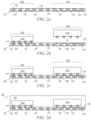
The number of slot lines and beam width overlap depends on slot width W1. There may be more than 3 slot lines or less than 3 slot lines. A wider slot width W1 generally involves more slot lines, while a narrower slot width W1 uses fewer slot lines.
In another embodiment, slot lines 180, 182, and 184 define a location where slot 150 is to be formed in electromagnetic shielding layer 142. Slot lines 180-184 are marked, imprinted, or projected on surface 156 of electromagnetic shielding layer 142 for slot 150. In this case, laser beam 160 follows a back and forth or zig-zag pattern or path. In a first pass, laser 162 is focused to follow slot line 180 as the right boundary and slot line 182 as the left boundary in the direction of arrow 186, as shown in FIG. 7 a . In a second pass, laser 162 is focused to follow slot line 182 as the left boundary and slot line 184 as the right boundary in the direction of arrow 188 opposite the direction of arrow 186, as shown in FIG. 7 b . Slot lines 180-184, as marked, imprinted, or projected on surface 156, serve as guides for laser beam 160 originating from laser 162. Laser 162 is focused on slot lines 180-184 so that laser beam 160 tracks in a zig-zag pattern, cutting back and forth in opposing directions, with clearly defined left boundary and right boundary on each pass. Laser beam 160 cuts or forms slot 150 along slot lines 180-184, similar to FIG. 4 . Multiple slot lines 180-184 provide focus for laser 162 to control slot width, slot depth, and slot edge quality, which are important to neutralize or block the EMI loop current flow through electromagnetic shielding layer 142 and reduce or inhibit EMI, RFI, and other inter-device interference in sensitive neighboring components within or adjacent to SIP module 138.
Electronic device 300 can be a stand-alone system that uses the semiconductor packages to perform one or more electrical functions. Alternatively, electronic device 300 can be a subcomponent of a larger system. For example, electronic device 300 can be part of a tablet, cellular phone, digital camera, communication system, or other electronic device. Alternatively, electronic device 300 can be a graphics card, network interface card, or other signal processing card that can be inserted into a computer. The semiconductor package can include microprocessors, memories, ASIC, logic circuits, analog circuits, RF circuits, discrete devices, or other semiconductor die or electrical components. Miniaturization and weight reduction are essential for the products to be accepted by the market. The distance between semiconductor devices may be decreased to achieve higher density.
In FIG. 9 , PCB 302 provides a general substrate for structural support and electrical interconnect of the semiconductor packages mounted on the PCB. Conductive signal traces 304 are formed over a surface or within layers of PCB 302 using evaporation, electrolytic plating, electroless plating, screen printing, or other suitable metal deposition process. Signal traces 304 provide for electrical communication between each of the semiconductor packages, mounted components, and other external system components. Traces 304 also provide power and ground connections to each of the semiconductor packages.
In some embodiments, a semiconductor device has two packaging levels. First level packaging is a technique for mechanically and electrically attaching the semiconductor die to an intermediate substrate. Second level packaging involves mechanically and electrically attaching the intermediate substrate to the PCB. In other embodiments, a semiconductor device may only have the first level packaging where the die is mechanically and electrically mounted directly to the PCB.
For the purpose of illustration, several types of first level packaging, including bond wire package 306 and flipchip 308, are shown on PCB 302. Additionally, several types of second level packaging, including ball grid array (BGA) 310, bump chip carrier (BCC) 312, land grid array (LGA) 316, multi-chip module (MCM) or SIP 318, quad flat non-leaded package (QFN) 320, quad flat package 322, embedded wafer level ball grid array (eWLB) 324, and wafer level chip scale package (WLCSP) 326 are shown mounted on PCB 302. In one embodiment, eWLB 324 is a fan-out wafer level package (Fo-WLP) and WLCSP 326 is a fan-in wafer level package (Fi-WLP). Depending upon the system requirements, any combination of semiconductor packages, configured with any combination of first and second level packaging styles, as well as other electronic components, can be connected to PCB 302. In some embodiments, electronic device 300 includes a single attached semiconductor package, while other embodiments call for multiple interconnected packages. By combining one or more semiconductor packages over a single substrate, manufacturers can incorporate pre-made components into electronic devices and systems. Because the semiconductor packages include sophisticated functionality, electronic devices can be manufactured using less expensive components and a stream-lined manufacturing process. The resulting devices are less likely to fail and less expensive to manufacture resulting in a lower cost for consumers.
While one or more embodiments of the present invention have been illustrated in detail, the skilled artisan will appreciate that modifications and adaptations to those embodiments may be made without departing from the scope of the present invention as set forth in the following claims.
Claims (31)
1. A method of forming a semiconductor device, comprising:
providing a semiconductor package;
forming a shielding layer over the semiconductor package;
providing a plurality of slot lines on the shielding layer defining a location to form a slot in the shielding layer; and
forming the slot in the shielding layer by cutting at the location along the plurality of slot lines.
2. The method of claim 1 , further including providing a laser to cut along the plurality of slot lines.
3. The method of claim 2 , further including providing a scanner to read the plurality of slot lines and control the laser to cut along the plurality of slot lines.
4. The method of claim 1 , wherein the plurality of slot lines include a left boundary slot line and a right boundary slot line.
5. The method of claim 1 , wherein forming the slot in the shielding layer includes:
performing an edge cut along the plurality of slot lines; and
performing a peel back along a center slot line to form the slot in the shielding layer.
6. The method of claim 1 , wherein forming the slot in the shielding layer includes:
performing a first cut in a first direction along the plurality of slot lines; and
performing a second cut in a second direction opposite the first direction along the plurality of slot lines to form the slot in the shielding layer.
7. A method of forming a semiconductor device, comprising:
forming a shielding layer over the semiconductor device;
providing a plurality of slot lines on the shielding layer; and
forming a slot in the shielding layer by cutting at the location along the plurality of slot lines.
8. The method of claim 7 , further including providing a laser to cut along the plurality of slot lines.
9. The method of claim 8 , further including providing a scanner to read the plurality of slot lines and control the laser to cut along the plurality of slot lines.
10. The method of claim 7 , wherein the plurality of slot lines include a left boundary slot line and a right boundary slot line.
11. The method of claim 7 , wherein forming the slot in the shielding layer includes:
performing an edge cut along the plurality of slot lines; and
performing a peel back along a center slot line to form the slot in the shielding layer.
12. The method of claim 7 , wherein forming the slot in the shielding layer includes:
performing a first cut in a first direction along the plurality of slot lines; and
performing a second cut in a second direction opposite the first direction along the plurality of slot lines to form the slot in the shielding layer.
13. The method of claim 7 , wherein forming the slot in the shielding layer includes a corner edge and vertical sidewalls.
14. A semiconductor device, comprising:
a semiconductor package; and
a shielding layer formed over the semiconductor package with a plurality of slot lines on the shielding layer defining a location to form a slot in the shielding layer at the location along the plurality of slot lines.
15. The semiconductor device of claim 14 , further including a laser to form the slot along the plurality of slot lines.
16. The semiconductor device of claim 15 , further including a scanner to read the plurality of slot lines and control the laser to form the slot along the plurality of slot lines.
17. The semiconductor device of claim 14 , wherein the plurality of slot lines include a left boundary slot line and a right boundary slot line.
18. The semiconductor device of claim 14 , wherein the slot in the shielding layer includes:
an edge cut along the plurality of slot lines; and
a peel back along a center slot line to form the slot in the shielding layer.
19. The semiconductor device of claim 14 , wherein the slot in the shielding layer includes:
a first cut in a first direction along the plurality of slot lines; and
a second cut in a second direction opposite the first direction along the plurality of slot lines to form the slot in the shielding layer.
20. A semiconductor device, comprising:
a shielding layer formed over the semiconductor device; and
a plurality of slot lines on the shielding layer defining a location for a slot formed in the shielding layer along the plurality of slot lines.
21. The semiconductor device of claim 20 , further including a laser to form the slot along the plurality of slot lines.
22. The semiconductor device of claim 21 , further including a scanner to read the plurality of slot lines and control the laser to form the slot along the plurality of slot lines.
23. The semiconductor device of claim 20 , wherein the plurality of slot lines include a left boundary slot line and a right boundary slot line.
24. The semiconductor device of claim 20 , wherein the slot in the shielding layer includes:
an edge cut along the plurality of slot lines; and
a peel back along a center slot line to form the slot in the shielding layer.
25. The semiconductor device of claim 20 , wherein the slot in the shielding layer includes:
a first cut in a first direction along the plurality of slot lines; and
a second cut in a second direction opposite the first direction along the plurality of slot lines to form the slot in the shielding layer.
26. A semiconductor device, comprising:
a semiconductor package; and
a shielding layer formed over the semiconductor package with a plurality of slot lines on the shielding layer defining a location to form a slot in the shielding layer at the location defined by the plurality of slot lines.
27. The semiconductor device of claim 26 , further including a laser to form the slot along the plurality of slot lines.
28. The semiconductor device of claim 27 , further including a scanner to read the plurality of slot lines and control the laser to form the slot along the plurality of slot lines.
29. The semiconductor device of claim 26 , wherein the plurality of slot lines include a left boundary slot line and a right boundary slot line.
30. The semiconductor device of claim 26 , wherein the slot in the shielding layer includes:
an edge cut along the plurality of slot lines; and
a peel back along a center slot line to form the slot in the shielding layer.
31. The semiconductor device of claim 26 , wherein the slot in the shielding layer includes:
a first cut in a first direction along the plurality of slot lines; and
a second cut in a second direction opposite the first direction along the plurality of slot lines to form the slot in the shielding layer.
Priority Applications (3)
| Application Number | Priority Date | Filing Date | Title |
|---|---|---|---|
| US17/307,437 US11640944B2 (en) | 2021-05-04 | 2021-05-04 | Semiconductor device and method of forming a slot in EMI shielding layer using a plurality of slot lines to guide a laser |
| CN202210324664.8A CN115295424B (en) | 2021-05-04 | 2022-03-30 | Method for forming grooves in EMI shielding layer using a plurality of slot lines to guide laser light and semiconductor device |
| KR1020220052466A KR20220151118A (en) | 2021-05-04 | 2022-04-28 | Semiconductor device and method of forming a slot in emi shielding layer using a plurality of slot lines to guide a laser |
Applications Claiming Priority (1)
| Application Number | Priority Date | Filing Date | Title |
|---|---|---|---|
| US17/307,437 US11640944B2 (en) | 2021-05-04 | 2021-05-04 | Semiconductor device and method of forming a slot in EMI shielding layer using a plurality of slot lines to guide a laser |
Publications (2)
| Publication Number | Publication Date |
|---|---|
| US20220359417A1 US20220359417A1 (en) | 2022-11-10 |
| US11640944B2 true US11640944B2 (en) | 2023-05-02 |
Family
ID=83819951
Family Applications (1)
| Application Number | Title | Priority Date | Filing Date |
|---|---|---|---|
| US17/307,437 Active 2041-06-05 US11640944B2 (en) | 2021-05-04 | 2021-05-04 | Semiconductor device and method of forming a slot in EMI shielding layer using a plurality of slot lines to guide a laser |
Country Status (3)
| Country | Link |
|---|---|
| US (1) | US11640944B2 (en) |
| KR (1) | KR20220151118A (en) |
| CN (1) | CN115295424B (en) |
Citations (6)
| Publication number | Priority date | Publication date | Assignee | Title |
|---|---|---|---|---|
| US9070793B2 (en) | 2010-08-02 | 2015-06-30 | Advanced Semiconductor Engineering, Inc. | Semiconductor device packages having electromagnetic interference shielding and related methods |
| US9129954B2 (en) | 2013-03-07 | 2015-09-08 | Advanced Semiconductor Engineering, Inc. | Semiconductor package including antenna layer and manufacturing method thereof |
| US9144183B2 (en) | 2013-07-31 | 2015-09-22 | Universal Scientific Industrial (Shanghai) Co., Ltd. | EMI compartment shielding structure and fabricating method thereof |
| US9153542B2 (en) | 2012-08-01 | 2015-10-06 | Advanced Semiconductor Engineering, Inc. | Semiconductor package having an antenna and manufacturing method thereof |
| US20160008923A1 (en) * | 2013-01-08 | 2016-01-14 | Hzo, Inc. | Removal of selected portions of protective coatings from substrates |
| US20200161252A1 (en) * | 2018-11-16 | 2020-05-21 | STATS ChipPAC Pte. Ltd. | Molded Laser Package with Electromagnetic Interference Shield and Method of Making |
Family Cites Families (6)
| Publication number | Priority date | Publication date | Assignee | Title |
|---|---|---|---|---|
| JP2005116844A (en) * | 2003-10-09 | 2005-04-28 | Matsushita Electric Ind Co Ltd | Method for manufacturing semiconductor device |
| KR101388181B1 (en) * | 2012-09-04 | 2014-04-30 | (주)하드램 | Laser cutting apparatus for glass substrate and method for cutting glass substrate |
| PT2974822T (en) * | 2014-07-14 | 2017-11-14 | Asm Tech Singapore Pte Ltd | Method of dicing thin semiconductor substrates |
| US10163808B2 (en) * | 2015-10-22 | 2018-12-25 | Avago Technologies International Sales Pte. Limited | Module with embedded side shield structures and method of fabricating the same |
| US9731965B1 (en) * | 2016-03-31 | 2017-08-15 | Stmicroelectronics S.R.L. | Dry scribing methods, devices and systems |
| US10985109B2 (en) * | 2018-12-27 | 2021-04-20 | STATS ChipPAC Pte. Ltd. | Shielded semiconductor packages with open terminals and methods of making via two-step process |
-
2021
- 2021-05-04 US US17/307,437 patent/US11640944B2/en active Active
-
2022
- 2022-03-30 CN CN202210324664.8A patent/CN115295424B/en active Active
- 2022-04-28 KR KR1020220052466A patent/KR20220151118A/en active IP Right Grant
Patent Citations (6)
| Publication number | Priority date | Publication date | Assignee | Title |
|---|---|---|---|---|
| US9070793B2 (en) | 2010-08-02 | 2015-06-30 | Advanced Semiconductor Engineering, Inc. | Semiconductor device packages having electromagnetic interference shielding and related methods |
| US9153542B2 (en) | 2012-08-01 | 2015-10-06 | Advanced Semiconductor Engineering, Inc. | Semiconductor package having an antenna and manufacturing method thereof |
| US20160008923A1 (en) * | 2013-01-08 | 2016-01-14 | Hzo, Inc. | Removal of selected portions of protective coatings from substrates |
| US9129954B2 (en) | 2013-03-07 | 2015-09-08 | Advanced Semiconductor Engineering, Inc. | Semiconductor package including antenna layer and manufacturing method thereof |
| US9144183B2 (en) | 2013-07-31 | 2015-09-22 | Universal Scientific Industrial (Shanghai) Co., Ltd. | EMI compartment shielding structure and fabricating method thereof |
| US20200161252A1 (en) * | 2018-11-16 | 2020-05-21 | STATS ChipPAC Pte. Ltd. | Molded Laser Package with Electromagnetic Interference Shield and Method of Making |
Also Published As
| Publication number | Publication date |
|---|---|
| CN115295424B (en) | 2024-04-19 |
| US20220359417A1 (en) | 2022-11-10 |
| KR20220151118A (en) | 2022-11-14 |
| CN115295424A (en) | 2022-11-04 |
Similar Documents
| Publication | Publication Date | Title |
|---|---|---|
| US10418332B2 (en) | Semiconductor device and method of forming partition fence and shielding layer around semiconductor components | |
| US11715703B2 (en) | EMI shielding for flip chip package with exposed die backside | |
| US11342294B2 (en) | Semiconductor device and method of forming protrusion e-bar for 3D SiP | |
| US20240088060A1 (en) | Semiconductor Device and Method of Stacking Devices Using Support Frame | |
| US20230343732A1 (en) | Semiconductor Device and Method of Forming Discrete Antenna Modules | |
| US11640944B2 (en) | Semiconductor device and method of forming a slot in EMI shielding layer using a plurality of slot lines to guide a laser | |
| US20230402397A1 (en) | Semiconductor Device and Method of Selective Shielding Using FOD Material | |
| US11450618B2 (en) | Semiconductor device and method of compartment shielding using bond wires | |
| US20230215721A1 (en) | Semiconductor Manufacturing Equipment and Method of Expelling Residue Through Suction Hood | |
| US11764136B2 (en) | Semiconductor device and method of forming bump pad array on substrate for ground connection for heat sink/shielding structure | |
| US11756897B2 (en) | Semiconductor device and method of forming a slot in EMI shielding with improved removal depth | |
| US20230395477A1 (en) | Semiconductor Device and Method of Disposing Electrical Components Over Side Surfaces of Interconnect Substrate | |
| US20240096807A1 (en) | Semiconductor Device and Method of Stacking Hybrid Substrates | |
| US20240063196A1 (en) | Semiconductor Device and Method of Forming Package with Double-Sided Integrated Passive Device | |
| US20240030154A1 (en) | Semiconductor Device and Method of Forming Conductive Structure for EMI Shielding and Heat Dissipation | |
| US20240105630A1 (en) | Semiconductor Device and Method of Stacking Hybrid Substrates with Embedded Electric Components | |
| US20240021536A1 (en) | Semiconductor Device and Method of Forming EMI Shielding Material in Two-Step Process to Avoid Contaminating Electrical Connector | |
| US20240021490A1 (en) | Semiconductor Device and Method of Forming Thin Heat Sink Using E-Bar Substrate |
Legal Events
| Date | Code | Title | Description |
|---|---|---|---|
| FEPP | Fee payment procedure |
Free format text: ENTITY STATUS SET TO UNDISCOUNTED (ORIGINAL EVENT CODE: BIG.); ENTITY STATUS OF PATENT OWNER: LARGE ENTITY |
|
| AS | Assignment |
Owner name: STATS CHIPPAC PTE. LTD., SINGAPORE Free format text: ASSIGNMENT OF ASSIGNORS INTEREST;ASSIGNORS:KIM, CHANGOH;JUNG, JINHEE;REEL/FRAME:056140/0725 Effective date: 20210505 |
|
| STPP | Information on status: patent application and granting procedure in general |
Free format text: RESPONSE TO NON-FINAL OFFICE ACTION ENTERED AND FORWARDED TO EXAMINER |
|
| STCF | Information on status: patent grant |
Free format text: PATENTED CASE |