WO2018180328A1 - 電動機制御装置 - Google Patents
電動機制御装置 Download PDFInfo
- Publication number
- WO2018180328A1 WO2018180328A1 PCT/JP2018/008891 JP2018008891W WO2018180328A1 WO 2018180328 A1 WO2018180328 A1 WO 2018180328A1 JP 2018008891 W JP2018008891 W JP 2018008891W WO 2018180328 A1 WO2018180328 A1 WO 2018180328A1
- Authority
- WO
- WIPO (PCT)
- Prior art keywords
- circuit
- voltage
- diode
- power supply
- inverter
- Prior art date
- Legal status (The legal status is an assumption and is not a legal conclusion. Google has not performed a legal analysis and makes no representation as to the accuracy of the status listed.)
- Ceased
Links
Images


Classifications
-
- B—PERFORMING OPERATIONS; TRANSPORTING
- B60—VEHICLES IN GENERAL
- B60T—VEHICLE BRAKE CONTROL SYSTEMS OR PARTS THEREOF; BRAKE CONTROL SYSTEMS OR PARTS THEREOF, IN GENERAL; ARRANGEMENT OF BRAKING ELEMENTS ON VEHICLES IN GENERAL; PORTABLE DEVICES FOR PREVENTING UNWANTED MOVEMENT OF VEHICLES; VEHICLE MODIFICATIONS TO FACILITATE COOLING OF BRAKES
- B60T13/00—Transmitting braking action from initiating means to ultimate brake actuator with power assistance or drive; Brake systems incorporating such transmitting means, e.g. air-pressure brake systems
- B60T13/74—Transmitting braking action from initiating means to ultimate brake actuator with power assistance or drive; Brake systems incorporating such transmitting means, e.g. air-pressure brake systems with electrical assistance or drive
-
- B—PERFORMING OPERATIONS; TRANSPORTING
- B60—VEHICLES IN GENERAL
- B60T—VEHICLE BRAKE CONTROL SYSTEMS OR PARTS THEREOF; BRAKE CONTROL SYSTEMS OR PARTS THEREOF, IN GENERAL; ARRANGEMENT OF BRAKING ELEMENTS ON VEHICLES IN GENERAL; PORTABLE DEVICES FOR PREVENTING UNWANTED MOVEMENT OF VEHICLES; VEHICLE MODIFICATIONS TO FACILITATE COOLING OF BRAKES
- B60T8/00—Arrangements for adjusting wheel-braking force to meet varying vehicular or ground-surface conditions, e.g. limiting or varying distribution of braking force
- B60T8/32—Arrangements for adjusting wheel-braking force to meet varying vehicular or ground-surface conditions, e.g. limiting or varying distribution of braking force responsive to a speed condition, e.g. acceleration or deceleration
- B60T8/34—Arrangements for adjusting wheel-braking force to meet varying vehicular or ground-surface conditions, e.g. limiting or varying distribution of braking force responsive to a speed condition, e.g. acceleration or deceleration having a fluid pressure regulator responsive to a speed condition
- B60T8/44—Arrangements for adjusting wheel-braking force to meet varying vehicular or ground-surface conditions, e.g. limiting or varying distribution of braking force responsive to a speed condition, e.g. acceleration or deceleration having a fluid pressure regulator responsive to a speed condition co-operating with a power-assist booster means associated with a master cylinder for controlling the release and reapplication of brake pressure through an interaction with the power assist device, i.e. open systems
-
- B—PERFORMING OPERATIONS; TRANSPORTING
- B60—VEHICLES IN GENERAL
- B60T—VEHICLE BRAKE CONTROL SYSTEMS OR PARTS THEREOF; BRAKE CONTROL SYSTEMS OR PARTS THEREOF, IN GENERAL; ARRANGEMENT OF BRAKING ELEMENTS ON VEHICLES IN GENERAL; PORTABLE DEVICES FOR PREVENTING UNWANTED MOVEMENT OF VEHICLES; VEHICLE MODIFICATIONS TO FACILITATE COOLING OF BRAKES
- B60T8/00—Arrangements for adjusting wheel-braking force to meet varying vehicular or ground-surface conditions, e.g. limiting or varying distribution of braking force
- B60T8/32—Arrangements for adjusting wheel-braking force to meet varying vehicular or ground-surface conditions, e.g. limiting or varying distribution of braking force responsive to a speed condition, e.g. acceleration or deceleration
- B60T8/88—Arrangements for adjusting wheel-braking force to meet varying vehicular or ground-surface conditions, e.g. limiting or varying distribution of braking force responsive to a speed condition, e.g. acceleration or deceleration with failure responsive means, i.e. means for detecting and indicating faulty operation of the speed responsive control means
-
- H—ELECTRICITY
- H02—GENERATION; CONVERSION OR DISTRIBUTION OF ELECTRIC POWER
- H02M—APPARATUS FOR CONVERSION BETWEEN AC AND AC, BETWEEN AC AND DC, OR BETWEEN DC AND DC, AND FOR USE WITH MAINS OR SIMILAR POWER SUPPLY SYSTEMS; CONVERSION OF DC OR AC INPUT POWER INTO SURGE OUTPUT POWER; CONTROL OR REGULATION THEREOF
- H02M7/00—Conversion of AC power input into DC power output; Conversion of DC power input into AC power output
- H02M7/42—Conversion of DC power input into AC power output without possibility of reversal
- H02M7/44—Conversion of DC power input into AC power output without possibility of reversal by static converters
- H02M7/48—Conversion of DC power input into AC power output without possibility of reversal by static converters using discharge tubes with control electrode or semiconductor devices with control electrode
-
- H—ELECTRICITY
- H02—GENERATION; CONVERSION OR DISTRIBUTION OF ELECTRIC POWER
- H02P—CONTROL OR REGULATION OF ELECTRIC MOTORS, ELECTRIC GENERATORS OR DYNAMO-ELECTRIC CONVERTERS; CONTROLLING TRANSFORMERS, REACTORS OR CHOKE COILS
- H02P27/00—Arrangements or methods for the control of AC motors characterised by the kind of supply voltage
- H02P27/04—Arrangements or methods for the control of AC motors characterised by the kind of supply voltage using variable-frequency supply voltage, e.g. inverter or converter supply voltage
- H02P27/06—Arrangements or methods for the control of AC motors characterised by the kind of supply voltage using variable-frequency supply voltage, e.g. inverter or converter supply voltage using DC to AC converters or inverters
Definitions
- the present invention relates to an electric motor control device suitable for use in, for example, an electric brake device.
- an electric brake device configured to electrically control a brake fluid pressure generated by a master cylinder.
- Such an electric brake device drives an electric motor (motor) by supplying power from a battery serving as a power source, and controls the brake fluid pressure.
- the battery also supplies power to a starter motor that performs an engine start operation. For this reason, when the battery voltage decreases due to the starter motor being driven when the engine is started, the motor of the electric brake device may not operate sufficiently and the braking force may decrease.
- Patent Document 1 discloses a configuration in which when the brake fluid pressure is supplied when the power supply voltage is lowered, the coil connection of the motor is short-circuited to maintain the brake fluid pressure.
- an inverter including a plurality of switching elements for example, MOSFETs
- MOSFETs switching elements
- the gate voltage of the MOSFET is insufficient before the driving power of the motor is insufficient, and the operation of the inverter may be disabled.
- the coil connection of the motor cannot be short-circuited, and the hydraulic pressure may be insufficient.
- the present invention has been made in view of the above-described problems of the prior art, and an object of the present invention is to provide an electric motor control device capable of expanding a low voltage region in which the electric motor can be controlled.
- an embodiment of the present invention includes an inverter that drives an electric motor, an inverter operating circuit that operates the inverter, a power storage device that supplies power to the inverter operating circuit, and the inverter operating circuit.
- An electric motor control device comprising: an arithmetic device to be controlled; and a step-up / step-down circuit that raises or lowers a voltage of the power storage device and supplies electric power to the arithmetic device, wherein the inverter operating circuit is also connected to the step-up / down circuit. Power supply is possible, and the power supply is received from the larger one of the voltage value supplied from the power storage device and the voltage value supplied from the step-up / down circuit. .
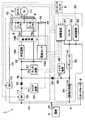
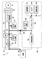
- FIG. 1 is a circuit diagram showing an electric brake device according to a first embodiment of the present invention.
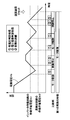
- FIG. 5 is a characteristic diagram showing temporal changes in the power supply voltage, the input voltage of the inverter operating circuit, the output voltage of the booster circuit, and the output voltage of the buck-boost circuit when the power supply voltage drops.
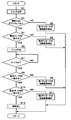
- 6 is a time chart showing the control contents of the electric motor when the power supply voltage fluctuates in the first embodiment and the comparative example of the present invention. It is a flowchart which shows the failure diagnosis process of the diode which the arithmetic unit in FIG. 1 performs. It is explanatory drawing which shows the application state of the voltage when the switch for inverter operation circuits is turned off in FIG.
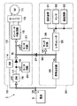
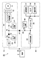
- FIG. 5 shows the principal part of the electric brake device by the 2nd Embodiment of this invention. It is explanatory drawing similar to FIG. 5 which shows the principal part of the electric brake device by the 3rd Embodiment of this invention.
- the electric brake device 1 applies a braking force to stop the vehicle.
- the electric brake device 1 is an electric booster (electrically booster) that electrically controls the brake fluid pressure generated in the master cylinder (M / C) 2 in order to supply brake fluid to a wheel cylinder (not shown) of a vehicle. Electric booster).
- the electric brake device 1 includes an electric motor 11 for controlling the brake fluid pressure and an arithmetic device 31 for controlling the electric motor 11.
- the electric brake device 1 includes a motor drive power supply system 10 for supplying drive power for the electric motor 11 and a logic drive power supply system 30 for supplying drive power for the arithmetic device 31.
- the motor drive power supply system 10 includes an electric motor 11, an inverter 12, an inverter operation circuit 15 and the like.
- the logic drive power supply system 30 includes an arithmetic unit 31, a step-up / down circuit 34, and the like.
- the power source 3 is a battery mounted on a vehicle, for example, and constitutes a power storage device.
- the power source 3 stores electric power of a generator (not shown) that is driven to rotate by an engine (not shown) formed of an internal combustion engine and generates electric power.
- the power source 3 is connected to a starter motor 5 which is an engine starting device via a power line 4. For this reason, the power supply 3 supplies electric power when the starter motor 5 is driven.
- the power source 3 supplies power to the electric motor 11 via the inverter 12.
- the power source 3 supplies power to the inverter operating circuit 15. Further, the power source 3 supplies power to the arithmetic device 31 and the like.
- the stroke sensor 6 is connected to the arithmetic unit 31.
- the stroke sensor 6 detects an operation (depression) amount of the brake pedal by the driver, and outputs a detection signal corresponding to the operation amount to the arithmetic device 31 as a braking request signal of the present invention.
- the motor drive power supply system 10 includes an electric motor 11, an inverter 12, an inverter operation circuit 15 and the like.
- the electric motor 11 outputs a braking force in response to a braking request signal.
- the electric motor 11 is configured as an electric motor of an electric booster composed of, for example, a DC brushless motor, and is driven and controlled by an arithmetic unit 31 described later.
- the electric motor 11 operates a piston (not shown) in the master cylinder 2 based on an operation (depression) amount of a brake pedal (not shown) to generate a brake fluid pressure in the master cylinder 2.
- the electric motor 11 is connected to the power source 3 via the inverter 12.
- the inverter 12 is configured using a plurality of switching elements S made of, for example, n-type MOSFETs.
- the inverter 12 converts the DC power from the power source 3 into AC power and supplies it to the electric motor 11. Thereby, the inverter 12 drives the electric motor 11.
- ON / OFF of each switching element S is controlled by the inverter operation circuit 15.
- the inverter 12 In the inverter 12, a circuit for one phase is formed by the high-side switching element S (upper arm) and the low-side switching element S (lower arm). For this reason, in order to control the three-phase electric motor 11, the inverter 12 comprises a circuit for three phases by a total of six switching elements S, for example.
- the low-side switching element S can be switched ON and OFF by applying the power supply voltage Vb from the power supply 3 to the gate.
- the switching element S on the high side needs to apply a voltage higher than the power supply voltage Vb to the gate because the source of the n-type MOSFET may rise to the power supply voltage level.
- the inverter 12 is connected to the power supply 3 via a power supply line 13 that is separate from the power supply line 4.
- a switch 14 is provided in the middle of the power line 13.
- the power source 3 supplies power to the inverter 12 when the switch 14 is turned on (connected state).
- the switch 14 is a fail-safe relay that stops power supply to the electric motor 11 and the inverter 12 when an abnormality occurs.
- the inverter operating circuit 15 operates the inverter 12. Specifically, the inverter operating circuit 15 is configured by a pre-driver IC, and controls ON / OFF of each switching element S of the inverter 12 based on a command from the arithmetic device 31. Thereby, the inverter operation circuit 15 controls the drive of the electric motor 11. The input side of the inverter operating circuit 15 is connected to the power source 3. The output side of the inverter operating circuit 15 is connected to the switching element S of the inverter 12.
- the inverter operating circuit 15 includes a booster circuit 15A, a drive circuit 15B, and a current sensor 15C.
- the booster circuit 15A is constituted by, for example, a charge pump circuit.
- the input side of the booster circuit 15A is connected to the power supply 3.
- the output side of the booster circuit 15A is connected to the gate of the high-side switching element S via the drive circuit 15B.
- the booster circuit 15A boosts the power supply voltage Vb and outputs a high-side gate voltage VgH higher than the power supply voltage Vb.
- the potential difference between the power supply voltage Vb and the high-side gate voltage VgH is set to a value larger than a predetermined value as a value at which the high-side switch element can be switched ON and OFF.
- the drive circuit 15B includes, for example, a plurality of switching elements (not shown).
- the drive circuit 15B connects or cuts off between the booster circuit 15A and the gate of the high-side switching element S (MOSFET), and switches between the power supply 3 and the low-side.
- the gate of the element S (MOSFET) is connected or cut off.
- the switching element of the drive circuit 15B is switched between ON (connected state) and OFF (blocked state) in accordance with a command from the arithmetic device 31. Thereby, the drive circuit 15B switches the application state of the high-side gate voltage VgH to the gate of the high-side switching element S.
- the drive circuit 15B switches the application state of the power supply voltage Vb that becomes the low-side gate voltage VgL to the gate of the low-side switching element S.
- the inverter operating circuit 15 controls ON / OFF of the switching element S of the inverter 12 to operate the inverter 12.
- the current sensor 15 ⁇ / b> C detects a current flowing through the electric motor 11 and outputs a detection signal to the arithmetic device 31.
- the input side of the current sensor 15C is connected to both ends of a current detection resistor 16 connected between the source of the low-side switching element S and the ground. At this time, the potential difference between both ends of the current detection resistor 16 becomes a value corresponding to the current flowing through the motor 11. Therefore, the current sensor 15C amplifies the potential difference between both ends of the current detection resistor 16 using the power supply voltage Vb, and outputs a detection signal corresponding to the potential difference to the arithmetic device 31.
- the inverter operating circuit 15 is connected to the power supply 3 via a power supply line 17 (first path) separate from the power supply lines 4 and 13. At this time, the power line 17 constitutes a first path that electrically connects the power source 3 and the inverter operating circuit 15.
- a switch 18 is provided in the middle of the power line 17. The power supply 3 supplies power to the inverter operating circuit 15 when the switch 18 is turned on (connected state).
- a first diode 19 is provided between the switch 18 and the inverter operating circuit 15.
- the first diode 19 allows a current in the direction from the power source 3 to the inverter operating circuit 15 and blocks a current in the reverse direction.
- the switch 18 is disposed on the power supply line 17 and connects or disconnects between the power supply 3 and the first diode 19. The switch 18 may suppress power supply from the power source 3 to the inverter operating circuit 15 when the electric motor 11 is not operating.
- a first monitor circuit 20 made of a voltage sensor is connected between the first diode 19 and the switch 18. At this time, the first monitor circuit 20 is disposed on the power supply line 17 and measures the voltage between the switch 18 and the first diode 19. Specifically, the first monitor circuit 20 detects the voltage V1 acting on the anode side of the first diode 19, and outputs a detection signal corresponding to the voltage V1 to the arithmetic unit 31.
- a third monitor circuit 21 made of a voltage sensor is connected between the first diode 19 and the inverter operating circuit 15. The third monitor circuit 21 detects the voltage V3 acting on the cathode side of the first diode 19 and outputs a detection signal corresponding to the voltage V3 to the arithmetic unit 31.
- the logic drive power supply system 30 includes an arithmetic unit 31, a step-up / down circuit 34, and the like.
- the arithmetic unit 31 controls the inverter operating circuit 15. Specifically, the arithmetic device 31 controls the electric motor 11 using the inverter operation circuit 15 and the inverter 12, and constitutes a part of the electric brake device 1.
- the arithmetic unit 31 is composed of a microcomputer (MCU), for example, and is driven by a drive voltage Vd generated by the step-up / step-down circuit 34 and the regulator 35.
- the arithmetic device 31 is a master pressure control unit that drives and controls the electric motor 11 of the electric booster to generate a brake fluid pressure in the master cylinder 2.
- a stroke sensor 6, a current sensor 15C, and monitor circuits 20, 21, and 38 are connected to the input side of the arithmetic unit 31.
- a sensor 32 made of a resolver or the like that detects the rotation angle of the electric motor 11 is connected to the input side of the arithmetic unit 31.
- an inverter operating circuit 15 (drive circuit 15B) and switches 14 and 18 are connected to the output side of the arithmetic unit 31.
- the arithmetic device 31 is connected to a communication circuit 33 for communicating with various controllers (not shown) provided in the vehicle through a CAN (Controller Area Network).
- the sensor 32 and the communication circuit 33 are also driven by the drive voltage Vd similarly to the arithmetic device 31.
- the arithmetic unit 31 receives the detection value of the stroke sensor 6 based on the operation of the brake pedal by the driver. Then, the arithmetic unit 31 operates the electric motor 11 based on the detection signal (braking request signal) of the stroke sensor 6 to generate the brake fluid pressure in the master cylinder 2.
- the arithmetic unit 31 includes a storage unit (not shown) including a ROM, a RAM, and the like, and the storage unit stores a diode failure diagnosis program shown in FIG.
- the arithmetic unit 31 executes the fault diagnosis processing program to change the voltages V1, V2, and V1 of the first monitor circuit 20, the second monitor circuit 38, and the third monitor circuit 21 when the switch 18 is switched. V3 is compared, and the abnormality of the first diode 19 and the second diode 37 is diagnosed.
- the step-up / step-down circuit 34 increases or decreases the power supply voltage Vb of the power supply 3 and supplies power to the arithmetic device 31.
- the step-up / step-down circuit 34 is constituted by, for example, a step-up / step-down chopper circuit (step-up / step-down DCDC circuit), and always outputs a constant output voltage Vc (DC voltage).
- the step-up / step-down circuit 34 increases or decreases the power supply voltage Vb supplied from the power supply 3 and converts the power supply voltage Vb into a predetermined constant output voltage Vc. For this reason, when the power supply voltage Vb is higher than the output voltage Vc, the step-up / down circuit 34 functions as a step-down circuit.
- the step-up / step-down circuit 34 functions as a booster circuit.
- the input side of the step-up / step-down circuit 34 is connected to the power source 3.
- the output side of the step-up / step-down circuit 34 is connected to the arithmetic unit 31, sensor 32, communication circuit 33, etc. via a regulator 35.
- the regulator 35 is, for example, a series regulator, removes ripples and the like from the output voltage Vc, and supplies a constant drive voltage Vd to the arithmetic unit 31 and the like.
- the output side of the step-up / step-down circuit 34 is connected to the inverter operating circuit 15 via an auxiliary power line 36.
- the auxiliary power line 36 constitutes a second path that electrically connects the power source 3 and the inverter operating circuit 15 via the step-up / step-down circuit 34.
- the step-up / step-down circuit 34 supplies power to the inverter operating circuit 15 and the arithmetic device 31.
- auxiliary power supply line 36 One end side of the auxiliary power supply line 36 is connected to the output side of the step-up / step-down circuit 34, and the other end side of the auxiliary power supply line 36 is connected to a middle position of the power supply line 17. For this reason, the auxiliary power supply line 36 joins the power supply line 17 and is electrically connected to the inverter operating circuit 15. At this time, a junction Pj between the auxiliary power supply line 36 and the power supply line 17 is located between the first diode 19 and the inverter operating circuit 15. For this reason, the first diode 19 is provided on the power supply line 17 between the junction Pj between the power supply line 17 and the auxiliary power supply line 36 and the power supply 3. For this reason, the third monitor circuit 21 connected to the cathode side of the first diode 19 detects the voltage V3 at the junction Pj.
- a second diode 37 is provided that allows current in the direction from the step-up / step-down circuit 34 to the inverter operating circuit 15 and blocks current in the reverse direction.
- the second diode 37 is provided between the junction Pj and the step-up / step-down circuit 34.
- the inverter operating circuit 15 can also supply power from the step-up / step-down circuit 34, and receives power supply from the power source 3 or the step-up / down circuit 34, whichever has a higher voltage value. That is, the inverter operating circuit 15 is supplied with power from the power source 3 through the auxiliary power line 36 when the power source voltage Vb of the power source 3 is lower than the output voltage Vc of the step-up / step-down circuit 34.
- a second monitor circuit 38 made of a voltage sensor is connected between the step-up / step-down circuit 34 and the second diode 37.
- the second monitor circuit 38 is disposed on the auxiliary power supply line 36 and measures the voltage between the step-up / step-down circuit 34 and the second diode 37.
- the second monitor circuit 38 detects the voltage V2 acting on the anode side of the second diode 37, and outputs a detection signal corresponding to the voltage V2 to the arithmetic unit 31.
- failure diagnosis processing for diagnosing failure of the diodes 19 and 37 by the arithmetic device 31 will be described with reference to FIGS.
- the failure diagnosis process shown in FIG. 4 is executed, for example, after the ignition switch of the vehicle is turned on and before the starter motor 5 is driven. Not limited to this, the failure diagnosis process may be executed immediately after the ignition switch is turned OFF, for example. Further, each step of the flowchart shown in FIG. 4 uses the notation “S”, for example, step 1 is indicated as “S1”.
- the arithmetic unit 31 executes the failure diagnosis process shown in FIG. 4 and detects the failure of the diodes 19 and 37.
- the arithmetic unit 31 turns off the switch 18 (cut off state) in S1, and cuts off the voltage supply to the anode side of the first diode 19.
- the normal power supply voltage Vb is higher than the output voltage Vc of the step-up / down circuit 34 (Vb> Vc).
- Vb the output voltage Vc of the step-up / down circuit 34
- the arithmetic unit 31 determines whether or not the voltage V1 measured by the first monitor circuit 20 is at the ground level.
- the arithmetic unit 31 determines “NO” in S ⁇ b> 2, proceeds to S ⁇ b> 3, and detects a short-circuit failure of the first diode 19.
- the arithmetic unit 31 determines whether or not the voltage V2 and the voltage V3 match.
- the arithmetic unit 31 determines “NO” in S4, proceeds to S5, and detects a disconnection failure of the second diode 37. When S5 ends, the process returns. On the other hand, if the second diode 37 is not disconnected, the potential difference between the voltage V2 and the voltage V3 is within a predetermined allowable value range, and the voltages V2 and V3 are approximately the same. At this time, the arithmetic unit 31 determines “YES” in S4, and proceeds to S6.
- the arithmetic unit 31 uses the voltage V1 measured by the first monitor circuit 20 and a predetermined value Vc0 determined as a target value when the step-up / step-down circuit 34 feedback-controls the output voltage Vc. It is determined whether or not it is too high.
- the arithmetic unit 31 determines “NO” in S7 and waits as it is.
- the arithmetic unit 31 determines “YES” in S7, and proceeds to S8.
- the power supply voltage Vb is supplied to the third monitor circuit 21 via the first diode 19. For this reason, if there is no disconnection failure in the first diode 19, the voltage V1 measured by the first monitor circuit 20 and the voltage V3 measured by the third monitor circuit 21 substantially coincide. Therefore, in S8, the arithmetic unit 31 determines whether or not the voltage V1 and the voltage V3 match.
- the arithmetic unit 31 determines “NO” in S ⁇ b> 8 and proceeds to S ⁇ b> 9 to detect a disconnection failure of the first diode 19. When S9 ends, the process returns. On the other hand, if the first diode 19 is not broken, the voltages V1 and V3 are substantially the same. At this time, the arithmetic unit 31 determines “YES” in S8, and proceeds to S10.
- the arithmetic unit 31 determines whether or not the voltage V2 measured by the second monitor circuit 38 and the specified value Vc0 corresponding to the output voltage Vc of the step-up / step-down circuit 34 match.
- the power supply voltage Vb higher than the output voltage Vc of the step-up / step-down circuit 34 is supplied to the second monitor circuit 38 through the switch 18 and the first diode 19. Therefore, the voltage V2 exceeds the predetermined allowable value and becomes higher than the specified value Vc0, and the voltage V2 becomes a value different from the specified value Vc0.
- the arithmetic unit 31 determines “NO” in S ⁇ b> 10, proceeds to S ⁇ b> 11, and detects a short-circuit failure of the second diode 37.
- the arithmetic unit 31 determines “YES” in S10, and proceeds to S12.
- S12 the first diode 19 has no short-circuit failure and disconnection failure
- the second diode 37 has no short-circuit failure and disconnection failure. For this reason, the arithmetic unit 31 determines that neither of the two diodes 19 and 37 has a failure and is in a normal state, and outputs a diagnosis result with no abnormality.
- the electric brake device 1 according to the present embodiment has the above-described configuration. Next, the operation of the electric brake device 1 will be described with reference to FIGS. 1 to 3.
- the arithmetic unit 31 controls the operation of the electric motor 11 based on the detection value of the stroke sensor 6 that detects the depression amount of the brake pedal.
- the brake fluid pressure generated in the master cylinder 2 by the operation of the electric motor 11 is distributed and supplied to the front and rear wheel brakes, and braking force is applied to the left and right front wheels and the left and right rear wheels, respectively. Is granted.
- the driver drives the starter motor 5 to start the engine while depressing the brake pedal.
- the starter motor 5 is driven by power supplied from the power source 3.
- the power source 3 supplies power to the inverter operating circuit 15. Therefore, if the voltage of the power supply 3 (power supply voltage Vb) temporarily decreases when the starter motor 5 is driven, the inverter operating circuit 15 may become inoperable, and the electric motor 11 and the brake fluid pressure may not be controlled.
- the inverter operating circuit 15 is supplied with power from both the power source 3 and the step-up / step-down circuit 34.
- the output voltage Vc of the step-up / step-down circuit 34 is supplied to the inverter operating circuit 15.
- the inverter operating circuit 15 when the power supply voltage Vb is normal (normal state), the power supply voltage Vb is higher than the output voltage Vc of the step-up / down circuit 34 (Vb> Vc). In this case, the inverter operating circuit 15 is supplied with the power supply voltage Vb via the first diode 19. At this time, the booster circuit 15A of the inverter operating circuit 15 operates with the power supply voltage Vb, and boosts the power supply voltage Vb to generate the high-side gate voltage VgH. For this reason, the inverter operating circuit 15 controls the switching element S of the inverter 12 using the high-side gate voltage VgH higher than the power supply voltage Vb and the low-side gate voltage VgL which is the same level as the power supply voltage Vb. Thereby, the inverter operation circuit 15 can control the operation of the electric motor 11 by switching ON / OFF of the switching element S made of MOSFET.
- the power supply voltage Vb when the starter motor 5 is driven, the power supply voltage Vb is lower than that in a normal state. In this manner, when the power supply voltage Vb is low (low voltage state), the power supply voltage Vb may be lower than the output voltage Vc of the step-up / down circuit 34 (Vb ⁇ Vc). In this case, the output voltage Vc of the step-up / step-down circuit 34 is supplied to the inverter operating circuit 15 via the second diode 37. At this time, the booster circuit 15A of the inverter operating circuit 15 operates by the output voltage Vc of the step-up / step-down circuit 34, and boosts the output voltage Vc to generate the high-side gate voltage VgH.
- the inverter operating circuit 15 controls the switching element S of the inverter 12 using the high-side gate voltage VgH higher than the power supply voltage Vb and the low-side gate voltage VgL at the same level as the output voltage Vc. Thereby, the inverter operation circuit 15 can control the operation of the electric motor 11 by switching ON / OFF of the switching element S made of MOSFET.
- the voltage Vt2 at which the step-up / step-down circuit 34 becomes inoperable is a lower value than the voltage Vt1 at which the inverter operation circuit 15 becomes inoperable.
- the low voltage region of the power supply voltage Vb that can be controlled by the electric motor 11 can be expanded to a voltage Vt2 lower than the voltage Vt1.
- the electric motor 11 can be controlled until the power supply voltage Vb decreases to the voltage Vt2 at which the step-up / step-down circuit 34 cannot operate.
- the arithmetic unit 31 can be operated until the step-up / step-down circuit 34 becomes inoperable.
- the power supply voltage Vb when the arithmetic unit 31 resets and the power supply voltage Vb which cannot use the inverter operation circuit 15 are the same value. As a result, it is not necessary to implement complicated control as in the comparative example.
- the output voltage Vc of the step-up / step-down circuit 34 is for operating the arithmetic unit 31 and the like, and is lower than the output voltage Vc of the step-up / down circuit 34 when the power supply voltage Vb is normal. Therefore, when the power supply voltage Vb is normal as shown in FIG. 2, there is a possibility that the switching element S on the high side of the inverter 12 cannot be controlled even if the output of the step-up / down circuit 34 is boosted by the booster circuit 15A. . Therefore, the second means has a problem that a voltage sufficient to drive the inverter 12 cannot be obtained when the power supply voltage Vb is normal.
- the inverter operating circuit 15 can be supplied with power from the step-up / down circuit 34 in addition to the power source 3, and the voltage value (power source voltage Vb) supplied from the power source 3 Power is supplied from the voltage value (output voltage Vc) supplied with power from the step-up / step-down circuit 34, whichever is larger.
- the inverter operating circuit 15 is supplied with the output voltage Vc higher than the voltage Vt1 from the step-up / down circuit 34.
- the step-up / step-down circuit 34 can operate until the power supply voltage Vb reaches a voltage Vt2 lower than the voltage Vt1.
- the inverter operating circuit 15 can operate until the power supply voltage Vb reaches the voltage Vt2 lower than the voltage Vt1, so that the low voltage region of the operable power supply voltage Vb can be widened.
- the operation of the inverter operating circuit 15 in the low voltage state can be stabilized.
- the inverter operating circuit 15 includes a power line 17 (first path) that is electrically connected to the power source 3 and an auxiliary power line 36 (second) that is electrically connected to the power source 3 via the step-up / down circuit 34.
- the inverter operating circuit 15 receives power supply from the power source 3 through the power line 17 when the power source voltage Vb of the power source 3 is higher than the output voltage Vc of the step-up / down circuit 34, and the step-up / down circuit
- the auxiliary power supply line 36 receives power from the step-up / step-down circuit 34. Supply.
- the step-up / step-down circuit 34 supplies power to the arithmetic unit 31 in a normal state where the power supply voltage Vb is higher than the output voltage Vc of the step-up / step-down circuit 34, and the power supply voltage Vb is higher than the output voltage Vc of the step-up / down circuit 34.
- Electric power is supplied to both the inverter operating circuit 15 and the arithmetic unit 31 in a low low voltage state. Thereby, the operation
- the step-up / step-down circuit 34 that supplies power to the arithmetic unit 31 can be used as a backup power source in a low voltage state. An increase in cost can be suppressed.
- the auxiliary power line 36 joins the power line 17 and is electrically connected to the inverter operating circuit 15.
- the junction point Pj between the power line 17 and the auxiliary power line 36 and the power source 3 are connected.
- a first diode 19 provided therebetween, and a second diode 37 provided between the junction Pj and the step-up / step-down circuit 34 are provided.
- the inverter operating circuit 15 is supplied with power from the power source 3 or the step-up / down circuit 34, whichever has the higher voltage value. can do.
- the operation of the inverter operating circuit 15 in the low voltage state of the power supply 3 can be stabilized with a simple circuit configuration.
- the power line 17 (first path) includes a switch 18 for connecting or disconnecting the power source 3 and the first diode 19, and a first voltage V 1 for measuring the voltage V 1 between the switch 18 and the first diode 19.
- the monitor circuit 20 is disposed, and a second monitor circuit 38 for measuring the voltage V3 between the step-up / step-down circuit 34 and the second diode 37 is disposed on the auxiliary power supply line (second path), and is connected to the junction Pj. It has the 3rd monitor circuit 21 which measures a voltage.
- the arithmetic unit 31 compares the voltages V1, V2, and V3 of the first monitor circuit 20, the second monitor circuit 38, and the third monitor circuit 21 when the switch 18 is switched, and the first diode 19 and the abnormality of the second diode 37 can be diagnosed.
- the arithmetic unit 31 compares the voltage V1 measured by the first monitor circuit 20 with the voltage V2 measured by the second monitor circuit 38, for example, with the switch 18 turned OFF, to thereby calculate the first value. A short-circuit abnormality of the diode 19 can be detected. Further, the arithmetic unit 31 compares the voltage V2 measured by the second monitor circuit 38 with the voltage V3 measured by the third monitor circuit 21, for example, with the switch 18 turned OFF, thereby the second diode 37. A disconnection abnormality can be detected.
- the arithmetic unit 31 compares the voltage V1 measured by the first monitor circuit 20 with the voltage V3 measured by the third monitor circuit 21, for example, with the switch 18 turned on, to thereby A disconnection abnormality can be detected. Further, the arithmetic unit 31 compares the voltage V2 measured by the second monitor circuit 38 and the voltage V3 measured by the third monitor circuit 21 with the switch 18 turned on, for example, so that the second diode 37 A short circuit abnormality can be detected.
- the switch 18 used for failure diagnosis is a switch for suppressing the current consumed by the inverter operating circuit 15 when the motor 11 is not started, and needs to be newly added to perform failure diagnosis of the diodes 19 and 37. There is no.
- the output voltage Vc of the step-up / step-down circuit 34 is used for the arithmetic unit 31, the sensor 32, the communication circuit 33, etc., so that the output voltage of the step-up / step-down circuit 34 becomes a specified value. Therefore, it is not necessary to add a new one in order to diagnose the failure of the diodes 19 and 37.
- the third monitor circuit 21 diagnoses whether or not a voltage that can operate the inverter operating circuit 15 is supplied, it is not necessary to newly add the third monitor circuit 21 to perform a failure diagnosis of the diodes 19 and 37. Only a first monitor circuit 20 provided between the switch 18 and the first diode 19 in the middle of the power supply line 17 needs to be newly added in order to perform failure diagnosis of the diodes 19 and 37. Thus, an increase in manufacturing cost can be suppressed.
- FIG. 7 shows a second embodiment of the present invention.
- the feature of this embodiment is that a plurality of first diodes and second diodes are connected in series.
- the same components as those in the first embodiment described above are denoted by the same reference numerals, and the description thereof is omitted.
- the electric brake device 41 according to the second embodiment is configured in substantially the same manner as the electric brake device 1 according to the first embodiment.
- two first diodes 19 are connected in series in the middle of the power line 17.
- two second diodes 37 are connected in series along the auxiliary power line 36. Note that the number of the first diodes 19 is not limited to two and may be three or more. Similarly, the number of second diodes 37 is not limited to two and may be three or more.
- the second embodiment it is possible to obtain the same operational effects as in the first embodiment. Further, when any one of the diodes 19 and 37 is short-circuited, the buck-boost circuit 34 may be broken. On the other hand, in the second embodiment, two first diodes 19 are connected in series, and two second diodes 37 are connected in series. For this reason, even when any one of the two first diodes 19 is short-circuited, the control of the electric motor 11 can be continued using the other one. The same applies to the second diode 37. For this reason, the reliability and durability of the electric brake device 41 can be improved.
- FIG. 8 shows a third embodiment of the present invention.
- a feature of this embodiment is that a fail-safe switch is provided between the power source and the inverter, and power is supplied from the power source to the inverter operating circuit via this switch.
- the same components as those in the first embodiment described above are denoted by the same reference numerals, and the description thereof is omitted.
- the electric brake device 51 according to the third embodiment is configured in substantially the same manner as the electric brake device 1 according to the first embodiment.
- the power supply line 17 (first path) has a branch power supply line 52 (third path) that branches from between the power supply 3 and the first diode 19 and supplies power from the power supply 3 to the inverter 12.
- the power supply line 17 includes a switch 53 for connecting or disconnecting the branch point Pb with the branch power supply line 52 and the power supply 3, and a first monitor for measuring a voltage between the switch 53 and the first diode 19.
- a circuit 20 is arranged.
- the switch 53 is a fail-safe relay that stops power supply to the electric motor 11 and the inverter 12 when an abnormality occurs. Further, the switch 53 suppresses power supply from the power source 3 to the inverter operating circuit 15 when the electric motor 11 is not operating.
- the arithmetic unit 31 has voltages V1, V2, V3 of the first monitor circuit 20, the second monitor circuit 38, and the third monitor circuit 21 when the switch 53 is switched. And the abnormality of the first diode 19 and the second diode 37 is diagnosed.
- the same operation and effect as in the first embodiment can be obtained.
- power is supplied to the inverter operating circuit 15 from the subsequent stage of the fail-safe switch 53 for cutting off the power supply to the inverter 12. Therefore, it is not necessary to add a new switch in order to detect the abnormality of the diodes 19 and 37, and the failure of the diodes 19 and 37 can be diagnosed by switching the fail-safe switch 53.
- the switch 18 according to the first embodiment can be omitted. For this reason, the structure of the whole apparatus can be simplified and manufacturing cost can be suppressed.
- the necessary braking force is calculated from the stroke amount of the brake pedal detected by the stroke sensor 6 as an example.
- the present invention is not limited to this.
- the necessary braking force may be calculated based on a braking force requested from a braking request from another external unit mounted on the vehicle.
- the required braking force may be calculated by detecting the state of the road where the vehicle is located.
- the inverter operating circuit 15 is supplied with power from the power source 3 or the step-up / down circuit 34, whichever has a higher voltage value. It was.
- the present invention is not limited to this.
- two switches are provided, and the arithmetic unit 31 determines whether the power supply voltage Vb and the output voltage Vc of the step-up / down circuit 34 are compared.
- a configuration may be adopted in which these two switches are switched ON and OFF.
- an inverter that drives an electric motor, an inverter operating circuit that operates the inverter, a power storage device that supplies power to the inverter operating circuit, an arithmetic device that controls the inverter operating circuit, and the power storage device
- a step-up / step-down circuit that increases or decreases the voltage to supply power to the arithmetic device, and the inverter operating circuit can also supply power from the step-up / down circuit.
- the power supply is received from the larger one of the voltage value supplied from the power storage device and the voltage value supplied from the step-up / down circuit.
- the inverter operating circuit is electrically connected to the power storage device via a first path electrically connected to the power storage device and the step-up / down circuit.
- the inverter operating circuit receives power supply from the power storage device through the first path when the voltage value of the power storage device is higher than the voltage value of the step-up / step-down circuit,
- the step-up / down circuit includes the inverter operating circuit, the arithmetic unit, It is characterized by supplying electric power to.
- the second path joins the first path and is electrically connected to the inverter operating circuit, and the first path on the first path. And a first diode provided between the junction of the second path and the power storage device, and a second diode provided between the junction and the buck-boost circuit. Yes.
- the first path has a switch for connecting or blocking between the power storage device and the first diode, and between the switch and the first diode.
- a first monitor circuit for measuring a voltage is disposed, and a second monitor circuit for measuring a voltage between the step-up / step-down circuit and the second diode is disposed in the second path, and the voltage at the junction point It has the 3rd monitor circuit which measures this.
- the voltages of the first monitor circuit, the second monitor circuit, and the third monitor circuit when the switch is switched are compared, and the first monitor circuit An abnormality between the diode and the second diode is diagnosed.
- the switch suppresses power supply from the power storage device to the inverter operating circuit when the electric motor is not operating.
- the first path has a third path that branches from between the power storage device and the first diode and supplies power of the power storage device to the inverter.
- the first path includes a switch for connecting or blocking between the branch point of the third path and the power storage device, and a first monitor circuit for measuring a voltage between the switch and the first diode.
- a second monitor circuit for measuring a voltage between the step-up / step-down circuit and the second diode is arranged in the second path, and a third monitor circuit for measuring the voltage at the junction is provided. And comparing the voltages of the first monitor circuit, the second monitor circuit, and the third monitor circuit when the switch is switched, and detecting an abnormality in the first diode and the second diode. Characterized by diagnosing That.
- the switch cuts off the power supply from the first path.
- a brake device based on the embodiment described above, for example, the following device can be considered.
- a brake device including an electric motor that outputs a braking force in response to a braking request signal, and an electric motor control device that controls the electric motor, wherein the electric motor control device drives the electric motor.
- An inverter an inverter operating circuit that operates the inverter, a power storage device that supplies power to the inverter operating circuit, an arithmetic device that controls the inverter operating circuit, and the arithmetic device that increases or decreases the voltage of the power storage device
- a step-up / step-down circuit for supplying electric power to the inverter operating circuit, the electric power supply from the step-up / down circuit is also possible, and the voltage value supplied from the power storage device and the step-up / down circuit It is characterized in that the power supply is received from the larger one of the voltage values to which power is supplied.
- the power storage device supplies power to a starting device of an internal combustion engine.
- this invention is not limited to the above-mentioned Example, Various modifications are included.
- the above-described embodiments have been described in detail for easy understanding of the present invention, and are not necessarily limited to those having all the configurations described.
- a part of the configuration of one embodiment can be replaced with the configuration of another embodiment, and the configuration of another embodiment can be added to the configuration of one embodiment.
Landscapes
- Engineering & Computer Science (AREA)
- Transportation (AREA)
- Mechanical Engineering (AREA)
- Power Engineering (AREA)
- Physics & Mathematics (AREA)
- Fluid Mechanics (AREA)
- Valves And Accessory Devices For Braking Systems (AREA)
- Braking Systems And Boosters (AREA)
- Regulating Braking Force (AREA)
- Control Of Ac Motors In General (AREA)
- Inverter Devices (AREA)
Abstract
ブレーキ装置1は、電動機11を駆動するインバータ12と、インバータ12を作動させるインバータ作動回路15と、インバータ作動回路15に電力供給する電源3と、インバータ作動回路15を制御する演算装置31と、電源3の電源電圧Vbを上昇または下降させて演算装置31に電力供給する昇降圧回路34とを有する。インバータ作動回路15は、昇降圧回路34からも電力供給が可能となっており、電源3の電源電圧Vbと昇降圧回路34の出力電圧Vcとのいずれか大きくなっている方から電力供給を受ける。
Description
本発明は、例えば電動ブレーキ装置等に用いて好適な電動機制御装置に関する。
四輪自動車等の車両に搭載されるブレーキ装置として、マスタシリンダで発生させるブレーキ液圧を電気的に制御する構成とした電動ブレーキ装置(電動倍力装置)が知られている。このような電動ブレーキ装置は、電源となるバッテリからの電力供給によって電動機(モータ)を駆動し、ブレーキ液圧を制御する。一方、バッテリは、エンジンの始動動作を行うスタータモータにも電力を供給する。このため、エンジン始動に伴うスタータモータの駆動によってバッテリ電圧が低下すると、電動ブレーキ装置のモータが十分に動作せず、制動力が低下する虞れがある。特許文献1には、電源電圧の低下時に、ブレーキ液圧が供給される場合には、モータのコイル結線を短絡させて、ブレーキ液圧を維持する構成が開示されている。
ところで、特許文献1に記載のブレーキ装置は、モータとバッテリとの間に、複数のスイッチング素子(例えば、MOSFET)からなるインバータが設けられ、このインバータを用いてモータを制御している。このとき、電源電圧が低下した低電圧領域では、モータの駆動電力が不足するよりも前に、MOSFETのゲート電圧が不足し、インバータの動作が不能になることがある。この結果、特許文献1に記載されたブレーキ装置では、モータのコイル結線を短絡させることができず、液圧が不足する可能性がある。
本発明は、上述した従来技術の問題に鑑みなされたもので、本発明の目的は、電動機の制御が可能な低電圧領域を広げることができる電動機制御装置を提供することにある。
上述した課題を解決するため、本発明の一実施形態は、電動機を駆動するインバータと、該インバータを作動させるインバータ作動回路と、該インバータ作動回路に電力供給する蓄電装置と、前記インバータ作動回路を制御する演算装置と、前記蓄電装置の電圧を上昇または下降させて前記演算装置に電力供給する昇降圧回路と、を有する電動機制御装置であって、前記インバータ作動回路は、前記昇降圧回路からも電力供給が可能となっており、前記蓄電装置から電力供給される電圧値と前記昇降圧回路から電力供給される電圧値とのいずれか大きくなっている方から電力供給を受けることを特徴としている。
本発明の一実施形態によれば、電動機の制御が可能な低電圧領域を広げることができる。
以下、実施形態による電動機制御装置を、四輪自動車の電動ブレーキ装置に適用した場合を例に挙げ、添付図面を参照して説明する。
図1において、電動ブレーキ装置1は、車両を停止させるために制動力を付与する。この電動ブレーキ装置1は、車両のホイールシリンダ(図示せず)にブレーキ液を供給するために、マスタシリンダ(M/C)2で発生させるブレーキ液圧を電気的に制御する電動倍力装置(電動式ブースタ)を構成している。このため、電動ブレーキ装置1は、ブレーキ液圧を制御するための電動機11と、電動機11を制御する演算装置31と、を備えている。
このとき、電動ブレーキ装置1は、電動機11の駆動電力を供給するためのモータ駆動用電源系統10と、演算装置31の駆動電力を供給するためのロジック駆動用電源系統30とを備えている。モータ駆動用電源系統10は、電動機11、インバータ12、インバータ作動回路15等を備えている。ロジック駆動用電源系統30は、演算装置31、昇降圧回路34等を備えている。
電源3は、例えば車両に搭載されたバッテリであり、蓄電装置を構成している。この電源3は、内燃機関からなるエンジン(図示せず)により回転駆動されて発電するジェネレータ(図示せず)の電力を蓄電する。電源3は、電源ライン4を介してエンジンの始動装置であるスタータモータ5に接続されている。このため、電源3は、スタータモータ5が駆動するときに電力を供給する。また、電源3は、インバータ12を介して電動機11に電力を供給する。これに加え、電源3は、インバータ作動回路15に電力を供給する。さらに、電源3は、演算装置31等にも電力を供給する。
また、演算装置31には、ストロークセンサ6が接続されている。ストロークセンサ6は、運転者によるブレーキペダルの操作(踏込み)量を検出し、この操作量に応じた検出信号を、本発明の制動要求信号として演算装置31に出力する。
次に、モータ駆動用電源系統10について説明する。モータ駆動用電源系統10は、電動機11、インバータ12、インバータ作動回路15等を備えている。
電動機11は、制動要求信号に応じて制動力を出力する。この電動機11は、例えばDCブラシレスモータからなる電動倍力装置の電動モータとして構成され、後述の演算装置31により駆動制御される。電動機11は、ブレーキペダル(図示せず)の操作(踏込み)量に基づき、マスタシリンダ2内のピストン(図示せず)を作動させてマスタシリンダ2内にブレーキ液圧を発生させる。
電動機11は、インバータ12を介して電源3に接続されている。インバータ12は、例えばn型のMOSFET等からなる複数のスイッチング素子Sを用いて構成されている。インバータ12は、電源3からの直流電力を交流電力に変換して電動機11に供給する。これにより、インバータ12は、電動機11を駆動する。ここで、インバータ12は、インバータ作動回路15によって、各スイッチング素子SのON/OFFが制御される。
また、インバータ12は、ハイサイドのスイッチング素子S(上アーム)とローサイドのスイッチング素子S(下アーム)とによって1相分の回路が形成される。このため、3相の電動機11を制御するためには、インバータ12は、例えば合計6個のスイッチング素子Sによって3相分の回路を構成している。
ローサイドのスイッチング素子Sは、n型のMOSFETのソースがグランドレベルとなるため、ゲートに電源3からの電源電圧Vbを印加することによって、ONとOFFの切換えが可能である。一方、ハイサイドのスイッチング素子Sは、n型のMOSFETのソースが電源電圧レベルまで上昇する可能性があるため、ゲートに電源電圧Vbよりも高い電圧を印加する必要がある。
インバータ12は、電源ライン4とは別個の電源ライン13を介して電源3に接続されている。電源ライン13の途中には、スイッチ14が設けられている。電源3は、スイッチ14がON(接続状態)となったときに、インバータ12に電力を供給する。スイッチ14は、異常発生時に、電動機11およびインバータ12への電力供給を停止するフェールセーフリレーである。
インバータ作動回路15は、インバータ12を作動させる。具体的には、インバータ作動回路15は、プリドライバICによって構成され、演算装置31からの指令に基づいて、インバータ12の各スイッチング素子SのON/OFFを制御する。これにより、インバータ作動回路15は、電動機11の駆動を制御する。インバータ作動回路15の入力側は、電源3に接続されている。インバータ作動回路15の出力側は、インバータ12のスイッチング素子Sに接続されている。また、インバータ作動回路15は、昇圧回路15Aと、駆動回路15Bと、電流センサ15Cとを備えている。
昇圧回路15Aは、例えばチャージポンプ回路によって構成されている。昇圧回路15Aの入力側は、電源3に接続されている。昇圧回路15Aの出力側は、駆動回路15Bを介して、ハイサイドのスイッチング素子Sのゲートに接続されている。昇圧回路15Aは、電源電圧Vbを昇圧し、電源電圧Vbよりも高い高側ゲート電圧VgHを出力する。このとき、電源電圧Vbと高側ゲート電圧VgHとの電位差は、ハイサイドのスイッチ素子がONとOFFが切換可能となる値として、予め決められた所定値よりも大きな値に設定されている。
駆動回路15Bは、例えば複数のスイッチング素子(図示せず)によって構成され、昇圧回路15Aとハイサイドのスイッチング素子S(MOSFET)のゲートとの間を接続または遮断すると共に、電源3とローサイドのスイッチング素子S(MOSFET)のゲートとの間を接続または遮断する。このとき、駆動回路15Bのスイッチング素子は、演算装置31からの指令に応じて、ON(接続状態)とOFF(遮断状態)とが切換わる。これにより、駆動回路15Bは、ハイサイドのスイッチング素子Sのゲートに対して、高側ゲート電圧VgHの印加状態を切り換える。これに加え、駆動回路15Bは、ローサイドのスイッチング素子Sのゲートに対して、低側ゲート電圧VgLとなる電源電圧Vbの印加状態を切り換える。これにより、インバータ作動回路15は、インバータ12のスイッチング素子SのON/OFFを制御し、インバータ12を作動させる。
電流センサ15Cは、電動機11に流れる電流を検出し、検出信号を演算装置31に出力する。電流センサ15Cの入力側は、ローサイドのスイッチング素子Sのソースとグランドとの間に接続された電流検出用抵抗16の両端に接続されている。このとき、電流検出用抵抗16の両端の電位差は、電動機11に流れる電流に対応した値になる。このため、電流センサ15Cは、電源電圧Vbを用いて、電流検出用抵抗16の両端の電位差を増幅し、電位差に応じた検出信号を演算装置31に出力する。
インバータ作動回路15は、電源ライン4,13とは別個の電源ライン17(第1経路)を介して電源3に接続されている。このとき、電源ライン17は、電源3とインバータ作動回路15とを電気的に接続する第1経路を構成している。電源ライン17の途中には、スイッチ18が設けられている。電源3は、スイッチ18がON(接続状態)となったときに、インバータ作動回路15に電力を供給する。
電源ライン17の途中には、スイッチ18とインバータ作動回路15との間に位置して、第1ダイオード19が設けられている。第1ダイオード19は、電源3からインバータ作動回路15に向かう方向の電流を許容し、逆方向の電流を遮断する。このとき、スイッチ18は、電源ライン17に配置され、電源3と第1ダイオード19との間を接続または遮断する。なお、スイッチ18は、電動機11の非動作時に、電源3からインバータ作動回路15への電力供給を抑制してもよい。
また、電源ライン17の途中には、第1ダイオード19とスイッチ18との間に位置して電圧センサからなる第1モニタ回路20が接続されている。このとき、第1モニタ回路20は、電源ライン17に配置され、スイッチ18と第1ダイオード19との間の電圧を測定している。具体的には、第1モニタ回路20は、第1ダイオード19のアノード側に作用する電圧V1を検出し、電圧V1に応じた検出信号を演算装置31に出力する。電源ライン17の途中には、第1ダイオード19とインバータ作動回路15との間に位置して電圧センサからなる第3モニタ回路21が接続されている。第3モニタ回路21は、第1ダイオード19のカソード側に作用する電圧V3を検出し、電圧V3に応じた検出信号を演算装置31に出力する。
次に、ロジック駆動用電源系統30について説明する。ロジック駆動用電源系統30は、演算装置31、昇降圧回路34等を備えている。
演算装置31は、インバータ作動回路15を制御する。具体的には、演算装置31は、インバータ作動回路15およびインバータ12を用いて、電動機11を制御するもので、電動ブレーキ装置1の一部を構成している。この演算装置31は、例えばマイクロコンピュータ(MCU)等からなり、昇降圧回路34およびレギュレータ35によって生成された駆動電圧Vdによって駆動する。演算装置31は、電動倍力装置の電動機11を駆動制御してマスタシリンダ2内にブレーキ液圧を発生させるマスタ圧制御ユニットとなっている。演算装置31の入力側には、ストロークセンサ6、電流センサ15C、モニタ回路20,21,38が接続されている。これに加え、演算装置31の入力側には、電動機11の回転角を検出するレゾルバ等からなるセンサ32が接続されている。一方、演算装置31の出力側には、インバータ作動回路15(駆動回路15B)、スイッチ14,18が接続されている。さらに、演算装置31は、CAN(Controller Area Network)を通じて車両内に設けられた各種のコントローラ(図示せず)と通信するための通信回路33に接続されている。センサ32および通信回路33も、演算装置31と同様に、駆動電圧Vdによって駆動する。
演算装置31は、運転者によるブレーキペダルの操作に基づくストロークセンサ6の検出値を受信する。そして、演算装置31は、ストロークセンサ6の検出信号(制動要求信号)に基づいて電動機11を作動させ、マスタシリンダ2内にブレーキ液圧を発生させる。また、演算装置31は、ROM、RAM等からなる記憶部(図示せず)を備え、この記憶部には、図4に示すダイオードの故障診断処理のプログラムが格納されている。演算装置31は、故障診断処理のプログラムを実行することによって、スイッチ18を切換えたときの、第1モニタ回路20と、第2モニタ回路38と、第3モニタ回路21との電圧V1,V2,V3を比較し、第1ダイオード19と第2ダイオード37との異常を診断する。
昇降圧回路34は、電源3の電源電圧Vbを上昇または下降させて、演算装置31に電力供給する。具体的には、昇降圧回路34は、例えば昇降圧チョッパ回路(昇降圧DCDC回路)によって構成され、常時一定の出力電圧Vc(直流電圧)を出力する。このとき、昇降圧回路34は、電源3から供給される電源電圧Vbを上昇または下降させ、電源電圧Vbを予め決められた一定の出力電圧Vcに変換する。このため、電源電圧Vbが出力電圧Vcよりも高いときには、昇降圧回路34は、降圧回路として機能する。逆に、電源電圧Vbが出力電圧Vcよりも低いときには、昇降圧回路34は、昇圧回路として機能する。このとき、昇降圧回路34の入力側は、電源3に接続されている。昇降圧回路34の出力側は、レギュレータ35を介して演算装置31、センサ32、通信回路33等に接続されている。レギュレータ35は、例えばシリーズレギュレータであり、出力電圧Vcからリップル等を除去し、演算装置31等に一定の駆動電圧Vdを供給する。
昇降圧回路34の出力側は、補助電源ライン36を介してインバータ作動回路15に接続されている。このとき、補助電源ライン36は、昇降圧回路34を介して電源3とインバータ作動回路15とを電気的に接続する第2経路を構成している。このため、昇降圧回路34は、インバータ作動回路15と演算装置31とに電力を供給する。
補助電源ライン36の一端側は、昇降圧回路34の出力側に接続され、補助電源ライン36の他端側は、電源ライン17の途中位置に接続されている。このため、補助電源ライン36は、電源ライン17に合流してインバータ作動回路15に電気的に接続されている。このとき、補助電源ライン36と電源ライン17との合流点Pjは、第1ダイオード19とインバータ作動回路15との間に位置している。このため、第1ダイオード19は、電源ライン17上で電源ライン17と補助電源ライン36との合流点Pjと電源3との間に設けられている。このため、第1ダイオード19のカソード側に接続された第3モニタ回路21は、合流点Pjの電圧V3を検出している。
補助電源ライン36の途中には、昇降圧回路34からインバータ作動回路15に向かう方向の電流を許容し、逆方向の電流を遮断する第2ダイオード37が設けられている。このとき、第2ダイオード37は、合流点Pjと昇降圧回路34との間に設けられている。これにより、インバータ作動回路15は、昇降圧回路34からも電力供給が可能となっており、電源3と昇降圧回路34とのいずれか大きい電圧値となっている方から電力供給を受ける。即ち、インバータ作動回路15は、電源3の電源電圧Vbが昇降圧回路34の出力電圧Vcよりも低いときに、補助電源ライン36で電源3から電力の供給を受ける。
また、補助電源ライン36の途中には、昇降圧回路34と第2ダイオード37との間に位置して電圧センサからなる第2モニタ回路38が接続されている。このとき、第2モニタ回路38は、補助電源ライン36に配置され、昇降圧回路34と第2ダイオード37との間の電圧を測定している。具体的には、第2モニタ回路38は、第2ダイオード37のアノード側に作用する電圧V2を検出し、電圧V2に応じた検出信号を演算装置31に出力する。
次に、演算装置31によってダイオード19,37の故障を診断する故障診断処理について、図4ないし図6を参照して説明する。なお、図4に示す故障診断処理は、例えば車両のイグニッションスイッチがON操作された後であって、スタータモータ5が駆動する前に実行される。これに限らず、故障診断処理は、例えばイグニッションスイッチをOFF操作した直後に実行してもよい。また、図4に示す流れ図のステップは、それぞれ「S」という表記を用い、例えばステップ1を「S1」として示すものである。
演算装置31は、図4に示す故障診断処理を実行し、ダイオード19,37の故障を検出する。故障診断処理を開始すると、演算装置31は、S1でスイッチ18をOFF(遮断状態)にし、第1ダイオード19のアノード側に対する電圧供給を遮断する。ここで、正常時の電源電圧Vbは、昇降圧回路34の出力電圧Vcよりも高い(Vb>Vc)。このため、図5に示すように、スイッチ18をOFFにすることで、第1ダイオード19のアノード側の電圧V1よりもカソード側の電圧V3が高い状態を作り出す。
このとき、第1ダイオード19が短絡故障していなければ、第1ダイオード19のカソード側からアノード側に電圧が供給されることはなく、第1モニタ回路20によって測定した電圧V1はグランドレベルまで低下する。そこで、続くS2では、演算装置31は、第1モニタ回路20によって測定した電圧V1がグランドレベルか否かを判定する。
第1ダイオード19が短絡故障している場合、電圧V1は、昇降圧回路34の出力電圧Vcに近い値になる。このとき、演算装置31は、S2で「NO」と判定し、S3に移行して第1ダイオード19の短絡故障を検知する。
第1ダイオード19が短絡故障すると、電源3が低電圧の場合に昇降圧回路34の出力電圧Vcが昇降圧回路34の入力部に回り込み、昇降圧回路34の故障の原因となってしまう。このため、S3で第1ダイオード19の短絡故障を検知した場合は、演算装置31は、スイッチ18をOFFにして、昇降圧回路34の入力部に出力電圧Vcが回り込むのを防止する。S3が終了するとリターンする。一方、第1ダイオード19が短絡故障していなければ、電圧V1はグランドレベルになる。このとき、演算装置31は、S2で「YES」と判定し、S4に移行する。
スイッチ18がOFFのとき、第3モニタ回路21には、第2ダイオード37を介して昇降圧回路34の出力電圧Vcが供給される。このため、第2ダイオード37に切断故障がなければ、第3モニタ回路21で測定される電圧V3と第2モニタ回路38で測定される電圧V2とは、概ね一致する。そこで、S4では、演算装置31は、電圧V2と電圧V3とが一致しているか否かを判定する。
第2ダイオード37が切断故障している場合、電圧V2と電圧V3とは、第2ダイオード37による電圧降下や測定誤差等に基づく所定の許容値を越えて、互いに異なる値になる。このとき、演算装置31は、S4で「NO」と判定し、S5に移行して第2ダイオード37の切断故障を検知する。S5が終了するとリターンする。一方、第2ダイオード37が切断故障していなければ、電圧V2と電圧V3との電位差は所定の許容値の範囲内となり、電圧V2,V3は概ね一致する。このとき、演算装置31は、S4で「YES」と判定し、S6に移行する。
続くS6では、演算装置31は、スイッチ18をONに切換える。これにより、図6に示すように、第2ダイオード37のアノード側の電圧V2よりもカソード側の電圧V3が高い状態を作り出す。
但し、電源電圧Vbは、昇降圧回路34の出力電圧Vcよりも低い状態になっている可能性がある。このため、続くS7では、演算装置31は、第1モニタ回路20によって測定した電圧V1と、昇降圧回路34が出力電圧Vcをフィードバック制御するときの目標値として、予め決められた規定値Vc0よりも高いか否かを判定する。電圧V1が規定値Vc0よりも低いとき(V1≦Vc0)は、演算装置31は、S7で「NO」と判定し、そのまま待機する。一方、電圧V1が規定値Vc0よりも高いとき(V1>Vc0)には、演算装置31は、S7で「YES」と判定し、S8に移行する。
このとき、第3モニタ回路21には、第1ダイオード19を介して電源電圧Vbが供給される。このため、第1ダイオード19に切断故障がなければ、第1モニタ回路20で測定される電圧V1と第3モニタ回路21で測定される電圧V3とは、概ね一致する。そこで、S8では、演算装置31は、電圧V1と電圧V3とが一致しているか否かを判定する。
第1ダイオード19が切断故障している場合は、第3モニタ回路21には、昇降圧回路34の出力電圧Vcが供給される。このため、電圧V1と電圧V3とは、所定の許容値を越えて、互いに異なる値になる。このとき、演算装置31は、S8で「NO」と判定し、S9に移行して第1ダイオード19の切断故障を検知する。S9が終了するとリターンする。一方、第1ダイオード19が切断故障していなければ、電圧V1,V3は概ね一致する。このとき、演算装置31は、S8で「YES」と判定し、S10に移行する。
スイッチ18がONのとき、第2ダイオード37が短絡故障していなければ、第2ダイオード37のカソード側からアノード側に電圧が供給されることはなく、第2モニタ回路38によって測定した電圧V2は、昇降圧回路34の出力電圧Vcと概ね一致する。そこで、続くS10では、演算装置31は、第2モニタ回路38によって測定した電圧V2と、昇降圧回路34の出力電圧Vcに対応した規定値Vc0とが一致しているか否かを判定する。
第2ダイオード37が短絡故障している場合、第2モニタ回路38には、スイッチ18および第1ダイオード19を通じて、昇降圧回路34の出力電圧Vcよりも高い電源電圧Vbが供給される。このため、電圧V2は、所定の許容値を越えて、規定値Vc0よりも高くなり、電圧V2は、規定値Vc0と異なる値になる。このとき、演算装置31は、S10で「NO」と判定し、S11に移行して第2ダイオード37の短絡故障を検知する。
第2ダイオード37が短絡故障すると、電源電圧Vbが昇降圧回路34の出力部に印加され、昇降圧回路34の故障の原因となってしまう。このため、第2ダイオード37の短絡故障を検知した場合は、スイッチ18をOFFにして、昇降圧回路34の出力部に電源電圧Vbが印加されるのを防止する。S11が終了するとリターンする。
一方、第2ダイオード37が短絡故障していなければ、電圧V2は、規定値Vc0と概ね一致する。このとき、演算装置31は、S10で「YES」と判定し、S12に移行する。S12に到達すると、第1ダイオード19に短絡故障および切断故障がなく、第2ダイオード37に短絡故障および切断故障がないことになる。このため、演算装置31は、2つのダイオード19,37のいずれにも故障がなく、正常な状態であると判定し、異常なしの診断結果を出力する。
本実施の形態による電動ブレーキ装置1は、上述の如き構成を有するもので、次に、電動ブレーキ装置1の動作について、図1ないし図3を参照して説明する。
車両の運転者がブレーキペダルを踏込み操作すると、演算装置31は、ブレーキペダルの踏込み量を検出するストロークセンサ6の検出値に基づいて電動機11の作動を制御する。そして、電動機11の作動によりマスタシリンダ2内に発生したブレーキ液圧は、前,後輪側ブレーキに分配して供給され、左,右の前輪と左,右の後輪とにそれぞれ制動力が付与される。
また、車両の起動時には、運転者はブレーキペダルを踏込み操作した状態で、スタータモータ5を駆動してエンジンを始動させる。このとき、スタータモータ5は、電源3から電力が供給されることにより駆動を行っている。これに加え、電源3は、インバータ作動回路15にも電力を供給している。従って、スタータモータ5の駆動時に一時的に電源3の電圧(電源電圧Vb)が低下すると、インバータ作動回路15が作動不能となり、電動機11およびブレーキ液圧の制御ができない虞がある。
そこで、本実施の形態では、インバータ作動回路15には、電源3と昇降圧回路34との両方から電力供給がなされている。そして、電源3の電圧が低下して、昇降圧回路34の出力電圧Vcが電源電圧Vbよりも高くなると、インバータ作動回路15には、昇降圧回路34の出力電圧Vcが供給される。これにより、電源電圧Vbが低下したときでも、電動機11の制御を継続させることができ、必要なブレーキ液圧を発生させることができる。
このような、電源電圧Vbとインバータ作動回路15との関係について、以下に詳細に説明する。
図2に示すように、電源電圧Vbが正常な状態(正常状態)では、電源電圧Vbは昇降圧回路34の出力電圧Vcよりも高い(Vb>Vc)。この場合、インバータ作動回路15には、第1ダイオード19を介して電源電圧Vbが供給される。このとき、インバータ作動回路15の昇圧回路15Aは、電源電圧Vbによって動作し、電源電圧Vbを昇圧して高側ゲート電圧VgHを生成する。このため、インバータ作動回路15は、電源電圧Vbよりも高い高側ゲート電圧VgHと、電源電圧Vbと同じ程度の低側ゲート電圧VgLとを用いて、インバータ12のスイッチング素子Sを制御する。これにより、インバータ作動回路15は、MOSFETからなるスイッチング素子SのON/OFFを切換えて、電動機11の作動を制御することができる。
一方、例えばスタータモータ5を駆動したときには、電源電圧Vbが正常な状態に比べて低下する。このように電源電圧Vbが低電圧になった状態(低電圧状態)では、電源電圧Vbは昇降圧回路34の出力電圧Vcよりも低くなることがある(Vb<Vc)。この場合、インバータ作動回路15には、第2ダイオード37を介して昇降圧回路34の出力電圧Vcが供給される。このとき、インバータ作動回路15の昇圧回路15Aは、昇降圧回路34の出力電圧Vcによって動作し、出力電圧Vcを昇圧して高側ゲート電圧VgHを生成する。このため、インバータ作動回路15は、電源電圧Vbよりも高い高側ゲート電圧VgHと、出力電圧Vcと同レベルの低側ゲート電圧VgLとを用いて、インバータ12のスイッチング素子Sを制御する。これにより、インバータ作動回路15は、MOSFETからなるスイッチング素子SのON/OFFを切換えて、電動機11の作動を制御することができる。
ここで、昇降圧回路34が作動不能となる電圧Vt2は、インバータ作動回路15が作動不能となる電圧Vt1に比べて低い値になっている。この結果、電動機11が制御可能となる電源電圧Vbの低電圧領域を、電圧Vt1よりも低い電圧Vt2まで広げることができる。これにより、電源電圧Vbが低下するときでも、昇降圧回路34の作動不能な電圧Vt2に低下するまでは、インバータ12、電流センサ15C等が作動し、電動機11の制御を継続することができる。
以上のような低電圧領域の拡張効果について、インバータ作動回路15に電源3からのみ電力を供給する比較例と対比して、図3を参照して詳細に説明する。このとき、比較例は、例えば、図1に示す本実施の形態の構成から、補助電源ライン36、第1ダイオード19および第2ダイオード37を省いたものになる。この比較例では、電源電圧Vbが低下すると、演算装置31がリセットする前にインバータ作動回路15が使用不能になる。このため、図3に示すように、電源電圧Vbが低電圧となった状態(低電圧状態)を検知して電動機11の制御を停止させる必要がある。これに加えて、電源電圧Vbが正常状態に復帰した場合は、電源電圧Vbの復帰を検知してインバータ作動回路15を初期化させる必要がある。このように、比較例では、電動機11等の制御が複雑になるだけでなく、電源電圧Vbの変動に伴って、電動機11の制御を復帰させるまでに時間を要してしまうという問題がある。
これに対し、本実施の形態では、電源電圧Vbが昇降圧回路34の作動不能な電圧Vt2に低下するまで、電動機11を制御することができる。このとき、昇降圧回路34は、演算装置31に駆動電力を供給するものであるから、昇降圧回路34が作動不能となるまで、演算装置31を動作させることができる。このため、本実施の形態では、演算装置31がリセットするときの電源電圧Vbと、インバータ作動回路15が使用不能となる電源電圧Vbとが、同じ値になっている。この結果、比較例のような複雑な制御を実装する必要がなくなる。
なお、インバータ作動回路15を低電圧でも作動可能にする第1の手段として、インバータ作動回路15の前段に昇圧回路を追加することも考えられる。しかしながら、この方法は本実施の形態と比較して、追加する部品点数が多く、コスト面で劣っている。
また、インバータ作動回路15を低電圧でも作動可能にする第2の手段として、昇降圧回路34の出力電圧Vcのみでインバータ作動回路15を作動させることも考えられる。しかしながら、昇降圧回路34の出力電圧Vcは演算装置31等を作動させるためのものであり、電源電圧Vbが正常な状態では、昇降圧回路34の出力電圧Vcよりも低い値になっている。このため、図2に示すように電源電圧Vbが正常な場合は、昇降圧回路34の出力を昇圧回路15Aで昇圧しても、インバータ12のハイサイドのスイッチング素子Sを制御できない可能性がある。従って、第2の手段は、電源電圧Vbが正常な場合には、インバータ12を駆動させるために十分な電圧を得ることができないという問題がある。
かくして、本実施の形態では、インバータ作動回路15は、電源3に加えて、昇降圧回路34からも電力供給が可能となっており、電源3から電力供給される電圧値(電源電圧Vb)と昇降圧回路34から電力供給される電圧値(出力電圧Vc)とのいずれか大きくなっている方から電力供給を受ける。
このため、電源電圧Vbがインバータ作動回路15の作動不能な電圧Vt1まで低下したときでも、インバータ作動回路15には、昇降圧回路34から電圧Vt1よりも高い出力電圧Vcが供給される。このとき、昇降圧回路34は、電源電圧Vbが電圧Vt1よりも低い電圧Vt2に到達するまで動作が可能である。この結果、インバータ作動回路15は、電源電圧Vbが電圧Vt1よりも低い電圧Vt2に到達するまで動作が可能となるから、動作可能な電源電圧Vbの低電圧領域を広げることができ、電源3の低電圧状態におけるインバータ作動回路15の作動を安定化させることができる。
また、インバータ作動回路15は、電源3と電気的に接続される電源ライン17(第1経路)と、昇降圧回路34を介して電源3と電気的に接続される補助電源ライン36(第2経路)と、を有し、インバータ作動回路15は、電源3の電源電圧Vbが昇降圧回路34の出力電圧Vcよりも高いときに、電源ライン17で電源3から電力供給を受け、昇降圧回路34の出力電圧Vcが電源3の電源電圧Vbよりも高いときに、補助電源ライン36で昇降圧回路34から電力供給を受け、昇降圧回路34は、インバータ作動回路15と演算装置31とに電力を供給する。
このため、昇降圧回路34は、電源電圧Vbが昇降圧回路34の出力電圧Vcよりも高い正常状態では、演算装置31に電力を供給し、電源電圧Vbが昇降圧回路34の出力電圧Vcより低い低電圧状態で、インバータ作動回路15と演算装置31の両方に電力を供給する。これにより、電源3の低電圧状態におけるインバータ作動回路15および演算装置31の両方の作動を安定化させることができる。これに加え、演算装置31に電力を供給する昇降圧回路34を、低電圧状態でのバックアップの電力源として使用することができるから、低電圧状態用に新たな電源を設ける必要がなく、製造コストの上昇を抑制することができる。
また、補助電源ライン36は、電源ライン17に合流してインバータ作動回路15に電気的に接続されており、電源ライン17上で電源ライン17と補助電源ライン36の合流点Pjと電源3との間に設けられた第1ダイオード19と、合流点Pjと昇降圧回路34との間に設けられた第2ダイオード37と、を備えている。
これにより、補助電源ライン36および2つのダイオード19,37を追加するだけで、インバータ作動回路15には、電源3と昇降圧回路34とのいずれか大きい電圧値となっている方から電力を供給することができる。この結果、簡易な回路構成で、電源3の低電圧状態におけるインバータ作動回路15の作動を安定化させることができる。
また、電源ライン17(第1経路)には、電源3と第1ダイオード19との間を接続または切断するスイッチ18と、スイッチ18と第1ダイオード19との間の電圧V1を測定する第1モニタ回路20とが配置され、補助電源ライン(第2経路)には、昇降圧回路34と第2ダイオード37との間の電圧V3を測定する第2モニタ回路38が配置され、合流点Pjの電圧を測定する第3モニタ回路21を有している。
これにより、演算装置31は、スイッチ18を切換えたときの、第1モニタ回路20と、第2モニタ回路38と、第3モニタ回路21との電圧V1,V2,V3を比較し、第1ダイオード19と第2ダイオード37との異常を診断することができる。
具体的には、演算装置31は、スイッチ18をOFFにした状態で、例えば第1モニタ回路20によって測定した電圧V1と第2モニタ回路38によって測定した電圧V2とを比較することによって、第1ダイオード19の短絡異常を検出することができる。また、演算装置31は、スイッチ18をOFFにした状態で、例えば第2モニタ回路38によって測定した電圧V2と第3モニタ回路21によって測定した電圧V3とを比較することによって、第2ダイオード37の切断異常を検出することができる。
また、演算装置31は、スイッチ18をONにした状態で、例えば第1モニタ回路20によって測定した電圧V1と第3モニタ回路21によって測定した電圧V3とを比較することによって、第1ダイオード19の切断異常を検出することができる。また、演算装置31は、スイッチ18をONにした状態で、例えば第2モニタ回路38によって測定した電圧V2と第3モニタ回路21によって測定した電圧V3とを比較することによって、第2ダイオード37の短絡異常を検出することができる。
また、故障診断に用いるスイッチ18は、電動機11が非起動時にインバータ作動回路15で消費される電流を抑制するためのスイッチであり、ダイオード19,37の故障診断を行うために新たに追加する必要はない。また、第2モニタ回路38は、昇降圧回路34の出力電圧Vcが演算装置31、センサ32、通信回路33等に使用されていることから、昇降圧回路34の出力電圧が規定の値となっているかを診断するものであるため、ダイオード19,37の故障診断を行うために新たに追加する必要はない。さらに、第3モニタ回路21は、インバータ作動回路15が作動可能な電圧が供給されているかを診断するものであるため、ダイオード19,37の故障診断を行うために新たに追加する必要はない。ダイオード19,37の故障診断を行うために新たに追加する必要があるのは、電源ライン17の途中で、スイッチ18と第1ダイオード19との間に設けられた第1モニタ回路20のみであり、製造コストの上昇を抑制することができる。
次に、図7は本発明の第2の実施の形態を示している。本実施の形態の特徴は、第1ダイオード、第2ダイオードをいずれも複数個直列に接続したことにある。なお、本実施の形態では、上述した第1の実施の形態と同一の構成要素に同一符号を付し、その説明を省略するものとする。
第2の実施の形態による電動ブレーキ装置41は、第1の実施の形態による電動ブレーキ装置1とほぼ同様に構成されている。但し、電源ライン17の途中には、2個の第1ダイオード19が直列に接続されている。また、補助電源ライン36の途中には、2個の第2ダイオード37が直列に接続されている。なお、第1ダイオード19の個数は、2個に限らず、3個以上でもよい。同様に、第2ダイオード37の個数は、2個に限らず、3個以上でもよい。
かくして、第2の実施の形態でも、第1の実施の形態と同様の作用効果を得ることができる。また、ダイオード19,37のいずれかが短絡故障した場合には、昇降圧回路34の故障を引き起こす可能性がある。これに対し、第2の実施の形態では、第1ダイオード19を2個直列に接続し、第2ダイオード37を2個直列に接続した。このため、2個の第1ダイオード19のうちいずれか一方が短絡故障したときでも、他方を用いて電動機11の制御を継続することができる。この点は、第2ダイオード37も同様である。このため、電動ブレーキ装置41の信頼性および耐久性を高めることができる。
次に、図8は本発明の第3の実施の形態を示している。本実施の形態の特徴は、電源とインバータとの間にフェールセーフ用のスイッチを設け、このスイッチを介してインバータ作動回路に電源からの電力供給を行う構成としたことにある。なお、本実施の形態では、上述した第1の実施の形態と同一の構成要素に同一符号を付し、その説明を省略するものとする。
第3の実施の形態による電動ブレーキ装置51は、第1の実施の形態による電動ブレーキ装置1とほぼ同様に構成されている。但し、電源ライン17(第1経路)は、電源3と第1ダイオード19との間から分岐し、電源3の電力をインバータ12に供給する分岐電源ライン52(第3経路)を有している。また、電源ライン17には、分岐電源ライン52との分岐点Pbと電源3との間を接続または遮断するスイッチ53と、スイッチ53と第1ダイオード19との間の電圧を測定する第1モニタ回路20とが配置されている。このとき、スイッチ53は、異常発生時に、電動機11およびインバータ12への電力供給を停止するフェールセーフリレーである。また、スイッチ53は、電動機11の非動作時に、電源3からインバータ作動回路15への電力供給を抑制する。
演算装置31は、第1の実施の形態と同様に、スイッチ53を切換えたときの、第1モニタ回路20と、第2モニタ回路38と、第3モニタ回路21との電圧V1,V2,V3を比較し、第1ダイオード19と第2ダイオード37との異常を診断する。
かくして、第3の実施の形態でも、第1の実施の形態と同様の作用効果を得ることができる。また、第3の実施の形態では、インバータ12への電源供給を遮断するためのフェールセーフ用のスイッチ53の後段からインバータ作動回路15に電源を供給する構成とした。このため、ダイオード19,37の異常を検出するために、新たなスイッチを追加する必要がなく、フェールセーフ用のスイッチ53を切換えることによって、ダイオード19,37の故障を診断することができる。これに加えて、第1の実施の形態によるスイッチ18を省くことができる。このため、装置全体の構成を簡略化して製造コストを抑制することができる。
なお、前記第1の実施の形態では、ストロークセンサ6が検出したブレーキペダルのストローク量から必要な制動力を算出した場合を例に挙げて説明した。しかし、本発明はこれに限らず、例えば車両に搭載された他の外部ユニットからの制動要求から要求される制動力により必要な制動力を算出してもよい。また、車両が位置している道路の状態を検出して要求される制動力を算出してもよい。これらは、第2,第3の実施の形態についても同様に適用が可能である。
前記第1の実施の形態では、2つのダイオード19,37を用いて、インバータ作動回路15が、電源3と昇降圧回路34とのいずれか大きい電圧値となっている方から電力供給を受ける構成とした。本発明はこれに限らず、例えば2つのダイオード19,37に代えて、2つのスイッチを設け、演算装置31が、電源電圧Vbと昇降圧回路34の出力電圧Vcとの比較結果に応じて、これら2つのスイッチのONとOFFを切換える構成としてもよい。
前記第1の実施の形態では、スイッチング素子SとしてMOSFETを用いた場合を例に挙げて説明したが、例えばIGBT等のような他のスイッチング素子を用いてもよい。この構成は、第2,第3の実施の形態についても同様に適用が可能である。
以上説明した実施の態様に基づく電動機制御装置として、例えば以下に述べる態様のものが考えられる。
第1の態様としては、電動機を駆動するインバータと、該インバータを作動させるインバータ作動回路と、該インバータ作動回路に電力供給する蓄電装置と、前記インバータ作動回路を制御する演算装置と、前記蓄電装置の電圧を上昇または下降させて前記演算装置に電力供給する昇降圧回路と、を有する電動機制御装置であって、前記インバータ作動回路は、前記昇降圧回路からも電力供給が可能となっており、前記蓄電装置から電力供給される電圧値と前記昇降圧回路から電力供給される電圧値とのいずれか大きくなっている方から電力供給を受けることを特徴としている。
第2の態様としては、第1の態様において、前記インバータ作動回路は、前記蓄電装置と電気的に接続される第1経路と、前記昇降圧回路を介して前記蓄電装置と電気的に接続される第2経路と、を有し、前記インバータ作動回路は、前記蓄電装置の電圧値が前記昇降圧回路の電圧値よりも高いときに、前記第1経路で前記蓄電装置から電力供給を受け、前記昇降圧回路の電圧値が前記蓄電装置の電圧値よりも高いときに、前記第2経路で前記昇降圧回路から電力供給を受け、前記昇降圧回路は、前記インバータ作動回路と前記演算装置とに電力を供給することを特徴としている。
第3の態様としては、第2の態様において、前記第2経路は、前記第1経路に合流して前記インバータ作動回路に電気的に接続されており、前記第1経路上で前記第1経路と前記第2経路の合流点と前記蓄電装置との間に設けられた第1ダイオードと、前記合流点と前記昇降圧回路との間に設けられた第2ダイオードと、を備えることを特徴としている。
第4の態様としては、第2の態様において、前記第1経路には、前記蓄電装置と前記第1ダイオードとの間を接続または遮断するスイッチと、該スイッチと前記第1ダイオードとの間の電圧を測定する第1モニタ回路とが配置され、前記第2経路には、前記昇降圧回路と前記第2ダイオードとの間の電圧を測定する第2モニタ回路が配置され、前記合流点の電圧を測定する第3モニタ回路を有することを特徴としている。
第5の態様としては、第4の態様において、前記スイッチを切換えたときの、前記第1モニタ回路と、前記第2モニタ回路と、前記第3モニタ回路との電圧を比較し、前記第1ダイオードと前記第2ダイオードとの異常を診断することを特徴としている。
第6の態様としては、第4または第5の態様において、前記スイッチは、前記電動機の非動作時に、前記蓄電装置から前記インバータ作動回路への電力供給を抑制することを特徴としている。
第7の態様としては、第3の態様において、前記第1経路は、前記蓄電装置と前記第1ダイオードとの間から分岐し、前記蓄電装置の電力を前記インバータに供給する第3経路を有し、前記第1経路には、前記第3経路との分岐点と前記蓄電装置との間を接続または遮断するスイッチと、該スイッチと第1ダイオードとの間の電圧を測定する第1モニタ回路とが配置され、前記第2経路には、前記昇降圧回路と前記第2ダイオードとの間の電圧を測定する第2モニタ回路が配置され、前記合流点の電圧を測定する第3モニタ回路を有し、前記スイッチを切換えたときの、前記第1モニタ回路と、前記第2モニタ回路と、前記第3モニタ回路との電圧を比較し、前記第1ダイオードと前記第2ダイオードとの異常を診断することを特徴としている。
第8の態様としては、第7の態様において、前記診断で異常が検出された場合、前記スイッチで前記第1経路からの電力供給を遮断することを特徴としている。
また、以上説明した実施の態様に基づくブレーキ装置として、例えば以下に述べる態様のものが考えられる。
第9の態様としては、制動要求信号に応じて制動力を出力する電動機と、前記電動機を制御する電動機制御装置と、を備えたブレーキ装置であって、前記電動機制御装置は、電動機を駆動するインバータと、該インバータを作動させるインバータ作動回路と、該インバータ作動回路に電力供給する蓄電装置と、前記インバータ作動回路を制御する演算装置と、前記蓄電装置の電圧を上昇または下降させて前記演算装置に電力供給する昇降圧回路と、を有し、前記インバータ作動回路は、前記昇降圧回路からも電力供給が可能となっており、前記蓄電装置から電力供給される電圧値と前記昇降圧回路から電力供給される電圧値とのいずれか大きくなっている方から電力供給を受けることを特徴としている。
第10の態様としては、第9の態様において、前記蓄電装置は、内燃機関の始動装置に電力を供給することを特徴としている。
尚、本発明は上記した実施例に限定されるものではなく、様々な変形例が含まれる。例えば、上記した実施例は本発明を分かりやすく説明するために詳細に説明したものであり、必ずしも説明した全ての構成を備えるものに限定されるものではない。また、ある実施例の構成の一部を他の実施例の構成に置き換えることが可能であり、また、ある実施例の構成に他の実施例の構成を加えることも可能である。また、各実施例の構成の一部について、他の構成の追加・削除・置換をすることが可能である。
本願は、2017年3月29日付出願の日本国特許出願第2017-065158号に基づく優先権を主張する。2017年3月29日付出願の日本国特許出願第2017-065158号の明細書、特許請求の範囲、図面、及び要約書を含む全開示内容は、参照により本願に全体として組み込まれる。
1,41,51 電動ブレーキ装置(ブレーキ装置) 3 電源(蓄電装置) 5 スタータモータ(始動装置) 11 電動機 12 インバータ 15 インバータ作動回路 17 電源ライン(第1経路) 18,53 スイッチ 19 第1ダイオード 20 第1モニタ回路 21 第3モニタ回路 31 演算装置 34 昇降圧回路 35 レギュレータ 36 補助電源ライン(第2経路) 37 第2ダイオード 38 第2モニタ回路 52 分岐電源ライン
Claims (8)
- 電動機制御装置であって、該電動機制御装置は、
電動機を駆動するインバータと、
該インバータを作動させるインバータ作動回路と、
該インバータ作動回路に電力供給する蓄電装置と、
前記インバータ作動回路を制御する演算装置と、
前記蓄電装置の電圧を上昇または下降させて前記演算装置に電力供給する昇降圧回路と、を有しており、
前記インバータ作動回路は、前記昇降圧回路からも電力供給が可能となっており、前記蓄電装置から電力供給される電圧値と前記昇降圧回路から電力供給される電圧値とのいずれか大きくなっている方から電力供給を受けることを特徴とする電動機制御装置。 - 請求項1に記載の電動機制御装置において、
前記インバータ作動回路は、
前記蓄電装置と電気的に接続される第1経路と、
前記昇降圧回路を介して前記蓄電装置と電気的に接続される第2経路と、を有しており、
前記インバータ作動回路は、前記蓄電装置の電圧値が前記昇降圧回路の電圧値よりも高いときに、前記第1経路で前記蓄電装置から電力供給を受け、
また、前記インバータ作動回路は、前記昇降圧回路の電圧値が前記蓄電装置の電圧値よりも高いときに、前記第2経路で前記昇降圧回路から電力供給を受け、
前記昇降圧回路は、前記インバータ作動回路と前記演算装置とに電力を供給することを特徴とする電動機制御装置。 - 請求項2に記載の電動機制御装置において、
前記第2経路は、前記第1経路に合流して前記インバータ作動回路に電気的に接続されており、
前記電動機制御装置は、
前記第1経路上に設けられた第1ダイオードであって、前記第1経路と前記第2経路の合流点と、前記蓄電装置との間に設けられた前記第1ダイオードと、
前記合流点と前記昇降圧回路との間に設けられた第2ダイオードと、を備えることを特徴とする電動機制御装置。 - 請求項2に記載の電動機制御装置において、
前記第1経路には、前記蓄電装置と前記第1ダイオードとの間を接続または遮断するスイッチと、該スイッチと前記第1ダイオードとの間の電圧を測定する第1モニタ回路とが配置されており、
前記第2経路には、前記昇降圧回路と前記第2ダイオードとの間の電圧を測定する第2モニタ回路が配置されており、
前記電動機制御装置は、また、
前記合流点の電圧を測定する第3モニタ回路を有することを特徴とする電動機制御装置。 - 請求項4に記載の電動機制御装置において、
前記電動機制御装置は、前記スイッチを切換えたときの、前記第1モニタ回路と、前記第2モニタ回路と、前記第3モニタ回路との電圧を比較することによって、前記第1ダイオードと前記第2ダイオードとの異常を診断することを特徴とする電動機制御装置。 - 請求項4または5に記載の電動機制御装置において、
前記スイッチは、前記電動機の非動作時に、前記蓄電装置から前記インバータ作動回路への電力供給を抑制することを特徴とする電動機制御装置。 - 請求項3に記載の電動機制御装置において、
前記第1経路は、前記蓄電装置と前記第1ダイオードとの間から分岐した第3経路であって、前記蓄電装置の電力を前記インバータに供給する前記第3経路を有しており、
前記第1経路には、前記第3経路との分岐点と、前記蓄電装置との間を接続または遮断するスイッチと、該スイッチと第1ダイオードとの間の電圧を測定する第1モニタ回路とが配置されており、
前記第2経路には、前記昇降圧回路と前記第2ダイオードとの間の電圧を測定する第2モニタ回路が配置されており、
前記電動機制御装置は、前記合流点の電圧を測定する第3モニタ回路を有しており、
前記電動機制御装置は、前記スイッチを切換えたときの、前記第1モニタ回路と、前記第2モニタ回路と、前記第3モニタ回路との電圧を比較することによって、前記第1ダイオードと前記第2ダイオードとの異常を診断することを特徴とする電動機制御装置。 - 請求項7に記載の電動機制御装置において、
前記診断で異常が検出された場合、前記スイッチで前記第1経路からの電力供給を遮断することを特徴とする電動機制御装置。
Applications Claiming Priority (2)
| Application Number | Priority Date | Filing Date | Title |
|---|---|---|---|
| JP2017065158A JP2020096395A (ja) | 2017-03-29 | 2017-03-29 | 電動機制御装置 |
| JP2017-065158 | 2017-03-29 |
Publications (1)
| Publication Number | Publication Date |
|---|---|
| WO2018180328A1 true WO2018180328A1 (ja) | 2018-10-04 |
Family
ID=63677325
Family Applications (1)
| Application Number | Title | Priority Date | Filing Date |
|---|---|---|---|
| PCT/JP2018/008891 Ceased WO2018180328A1 (ja) | 2017-03-29 | 2018-03-08 | 電動機制御装置 |
Country Status (2)
| Country | Link |
|---|---|
| JP (1) | JP2020096395A (ja) |
| WO (1) | WO2018180328A1 (ja) |
Families Citing this family (2)
| Publication number | Priority date | Publication date | Assignee | Title |
|---|---|---|---|---|
| US12152912B2 (en) * | 2021-09-27 | 2024-11-26 | Rosemount Inc. | Wireless process variable transmitter with battery power source |
| JP7708054B2 (ja) * | 2022-09-26 | 2025-07-15 | トヨタ自動車株式会社 | 制御装置 |
Citations (4)
| Publication number | Priority date | Publication date | Assignee | Title |
|---|---|---|---|---|
| JP2008279953A (ja) * | 2007-05-11 | 2008-11-20 | Nsk Ltd | 電動パワーステアリング装置 |
| JP2015033272A (ja) * | 2013-08-05 | 2015-02-16 | 日立オートモティブシステムズ株式会社 | 電動モータの制御装置 |
| JP2016201910A (ja) * | 2015-04-10 | 2016-12-01 | 株式会社デンソー | 制御装置及び電動パワーステアリング装置 |
| WO2016194835A1 (ja) * | 2015-05-29 | 2016-12-08 | 日本電産株式会社 | 直流ブラシレスモータ制御装置 |
-
2017
- 2017-03-29 JP JP2017065158A patent/JP2020096395A/ja active Pending
-
2018
- 2018-03-08 WO PCT/JP2018/008891 patent/WO2018180328A1/ja not_active Ceased
Patent Citations (4)
| Publication number | Priority date | Publication date | Assignee | Title |
|---|---|---|---|---|
| JP2008279953A (ja) * | 2007-05-11 | 2008-11-20 | Nsk Ltd | 電動パワーステアリング装置 |
| JP2015033272A (ja) * | 2013-08-05 | 2015-02-16 | 日立オートモティブシステムズ株式会社 | 電動モータの制御装置 |
| JP2016201910A (ja) * | 2015-04-10 | 2016-12-01 | 株式会社デンソー | 制御装置及び電動パワーステアリング装置 |
| WO2016194835A1 (ja) * | 2015-05-29 | 2016-12-08 | 日本電産株式会社 | 直流ブラシレスモータ制御装置 |
Also Published As
| Publication number | Publication date |
|---|---|
| JP2020096395A (ja) | 2020-06-18 |
Similar Documents
| Publication | Publication Date | Title |
|---|---|---|
| JP5165394B2 (ja) | 車両用電源システム | |
| CN105471360B (zh) | 电动机驱动控制装置、动力转向装置、电动制动装置、电动泵装置 | |
| JP6358304B2 (ja) | 車両用電源装置 | |
| JP3705166B2 (ja) | ステアリング制御装置 | |
| CN101795926B (zh) | 转向装置 | |
| US9680405B2 (en) | Onboard motor controller | |
| JP5384397B2 (ja) | 電動式建設機械 | |
| US20170346436A1 (en) | Control apparatus of rotary electric machine and electric power steering apparatus using the same | |
| WO2018047636A1 (ja) | 車載用のバックアップ装置 | |
| WO2019208203A1 (ja) | 車載用のバックアップ回路及び車載用のバックアップ装置 | |
| CN105346593B (zh) | 电动助力转向系统 | |
| JP6971133B2 (ja) | 電動機制御装置 | |
| JP5024618B2 (ja) | 電動モータ制御装置及び電動倍力装置 | |
| US9982416B2 (en) | Shovel and method of controlling shovel | |
| WO2015141449A1 (ja) | 作業機械 | |
| WO2017203807A1 (ja) | ブレーキシステムおよび電動ブレーキ駆動装置 | |
| JP4325284B2 (ja) | 電圧変換装置 | |
| KR101914127B1 (ko) | 모터의 고장 감지 장치 | |
| JP5033443B2 (ja) | 電源回路及びこの電源回路を備えたブレーキ制御装置 | |
| JP2020096395A (ja) | 電動機制御装置 | |
| US9391545B2 (en) | Method and electronic device for improving the availability of an electromechanical actuator | |
| WO2023204081A1 (ja) | 負荷駆動装置 | |
| JP2019161991A (ja) | 電子制御装置 | |
| JP7041526B2 (ja) | 電子制御ユニットおよび制動制御装置 | |
| WO2019132002A1 (ja) | 電動式直動アクチュエータおよび電動ブレーキ装置 |
Legal Events
| Date | Code | Title | Description |
|---|---|---|---|
| 121 | Ep: the epo has been informed by wipo that ep was designated in this application |
Ref document number: 18775417 Country of ref document: EP Kind code of ref document: A1 |
|
| NENP | Non-entry into the national phase |
Ref country code: DE |
|
| 122 | Ep: pct application non-entry in european phase |
Ref document number: 18775417 Country of ref document: EP Kind code of ref document: A1 |
|
| NENP | Non-entry into the national phase |
Ref country code: JP |