WO2018159457A1 - 実装用基板 - Google Patents
実装用基板 Download PDFInfo
- Publication number
- WO2018159457A1 WO2018159457A1 PCT/JP2018/006515 JP2018006515W WO2018159457A1 WO 2018159457 A1 WO2018159457 A1 WO 2018159457A1 JP 2018006515 W JP2018006515 W JP 2018006515W WO 2018159457 A1 WO2018159457 A1 WO 2018159457A1
- Authority
- WO
- WIPO (PCT)
- Prior art keywords
- conductor
- mounting
- resin layer
- distance
- mounting substrate
- Prior art date
- Legal status (The legal status is an assumption and is not a legal conclusion. Google has not performed a legal analysis and makes no representation as to the accuracy of the status listed.)
- Ceased
Links
Images





Classifications
-
- H—ELECTRICITY
- H01—ELECTRIC ELEMENTS
- H01F—MAGNETS; INDUCTANCES; TRANSFORMERS; SELECTION OF MATERIALS FOR THEIR MAGNETIC PROPERTIES
- H01F27/00—Details of transformers or inductances, in general
- H01F27/06—Mounting, supporting or suspending transformers, reactors or choke coils not being of the signal type
-
- H—ELECTRICITY
- H01—ELECTRIC ELEMENTS
- H01F—MAGNETS; INDUCTANCES; TRANSFORMERS; SELECTION OF MATERIALS FOR THEIR MAGNETIC PROPERTIES
- H01F17/00—Fixed inductances of the signal type
- H01F17/0006—Printed inductances
- H01F17/0013—Printed inductances with stacked layers
-
- B—PERFORMING OPERATIONS; TRANSPORTING
- B06—GENERATING OR TRANSMITTING MECHANICAL VIBRATIONS IN GENERAL
- B06B—METHODS OR APPARATUS FOR GENERATING OR TRANSMITTING MECHANICAL VIBRATIONS OF INFRASONIC, SONIC, OR ULTRASONIC FREQUENCY, e.g. FOR PERFORMING MECHANICAL WORK IN GENERAL
- B06B1/00—Methods or apparatus for generating mechanical vibrations of infrasonic, sonic, or ultrasonic frequency
- B06B1/02—Methods or apparatus for generating mechanical vibrations of infrasonic, sonic, or ultrasonic frequency making use of electrical energy
- B06B1/04—Methods or apparatus for generating mechanical vibrations of infrasonic, sonic, or ultrasonic frequency making use of electrical energy operating with electromagnetism
- B06B1/045—Methods or apparatus for generating mechanical vibrations of infrasonic, sonic, or ultrasonic frequency making use of electrical energy operating with electromagnetism using vibrating magnet, armature or coil system
-
- H—ELECTRICITY
- H01—ELECTRIC ELEMENTS
- H01F—MAGNETS; INDUCTANCES; TRANSFORMERS; SELECTION OF MATERIALS FOR THEIR MAGNETIC PROPERTIES
- H01F27/00—Details of transformers or inductances, in general
- H01F27/28—Coils; Windings; Conductive connections
- H01F27/2804—Printed windings
-
- H—ELECTRICITY
- H01—ELECTRIC ELEMENTS
- H01F—MAGNETS; INDUCTANCES; TRANSFORMERS; SELECTION OF MATERIALS FOR THEIR MAGNETIC PROPERTIES
- H01F27/00—Details of transformers or inductances, in general
- H01F27/28—Coils; Windings; Conductive connections
- H01F27/29—Terminals; Tapping arrangements for signal inductances
- H01F27/292—Surface mounted devices
-
- H—ELECTRICITY
- H01—ELECTRIC ELEMENTS
- H01F—MAGNETS; INDUCTANCES; TRANSFORMERS; SELECTION OF MATERIALS FOR THEIR MAGNETIC PROPERTIES
- H01F41/00—Apparatus or processes specially adapted for manufacturing or assembling magnets, inductances or transformers; Apparatus or processes specially adapted for manufacturing materials characterised by their magnetic properties
- H01F41/02—Apparatus or processes specially adapted for manufacturing or assembling magnets, inductances or transformers; Apparatus or processes specially adapted for manufacturing materials characterised by their magnetic properties for manufacturing cores, coils, or magnets
- H01F41/04—Apparatus or processes specially adapted for manufacturing or assembling magnets, inductances or transformers; Apparatus or processes specially adapted for manufacturing materials characterised by their magnetic properties for manufacturing cores, coils, or magnets for manufacturing coils
-
- H—ELECTRICITY
- H01—ELECTRIC ELEMENTS
- H01F—MAGNETS; INDUCTANCES; TRANSFORMERS; SELECTION OF MATERIALS FOR THEIR MAGNETIC PROPERTIES
- H01F41/00—Apparatus or processes specially adapted for manufacturing or assembling magnets, inductances or transformers; Apparatus or processes specially adapted for manufacturing materials characterised by their magnetic properties
- H01F41/02—Apparatus or processes specially adapted for manufacturing or assembling magnets, inductances or transformers; Apparatus or processes specially adapted for manufacturing materials characterised by their magnetic properties for manufacturing cores, coils, or magnets
- H01F41/04—Apparatus or processes specially adapted for manufacturing or assembling magnets, inductances or transformers; Apparatus or processes specially adapted for manufacturing materials characterised by their magnetic properties for manufacturing cores, coils, or magnets for manufacturing coils
- H01F41/041—Printed circuit coils
-
- H—ELECTRICITY
- H01—ELECTRIC ELEMENTS
- H01F—MAGNETS; INDUCTANCES; TRANSFORMERS; SELECTION OF MATERIALS FOR THEIR MAGNETIC PROPERTIES
- H01F41/00—Apparatus or processes specially adapted for manufacturing or assembling magnets, inductances or transformers; Apparatus or processes specially adapted for manufacturing materials characterised by their magnetic properties
- H01F41/14—Apparatus or processes specially adapted for manufacturing or assembling magnets, inductances or transformers; Apparatus or processes specially adapted for manufacturing materials characterised by their magnetic properties for applying magnetic films to substrates
- H01F41/24—Apparatus or processes specially adapted for manufacturing or assembling magnets, inductances or transformers; Apparatus or processes specially adapted for manufacturing materials characterised by their magnetic properties for applying magnetic films to substrates from liquids
- H01F41/26—Apparatus or processes specially adapted for manufacturing or assembling magnets, inductances or transformers; Apparatus or processes specially adapted for manufacturing materials characterised by their magnetic properties for applying magnetic films to substrates from liquids using electric currents, e.g. electroplating
-
- H—ELECTRICITY
- H04—ELECTRIC COMMUNICATION TECHNIQUE
- H04R—LOUDSPEAKERS, MICROPHONES, GRAMOPHONE PICK-UPS OR LIKE ACOUSTIC ELECTROMECHANICAL TRANSDUCERS; ELECTRIC HEARING AIDS; PUBLIC ADDRESS SYSTEMS
- H04R31/00—Apparatus or processes specially adapted for the manufacture of transducers or diaphragms therefor
-
- H—ELECTRICITY
- H04—ELECTRIC COMMUNICATION TECHNIQUE
- H04R—LOUDSPEAKERS, MICROPHONES, GRAMOPHONE PICK-UPS OR LIKE ACOUSTIC ELECTROMECHANICAL TRANSDUCERS; ELECTRIC HEARING AIDS; PUBLIC ADDRESS SYSTEMS
- H04R9/00—Transducers of moving-coil, moving-strip, or moving-wire type
-
- H—ELECTRICITY
- H04—ELECTRIC COMMUNICATION TECHNIQUE
- H04R—LOUDSPEAKERS, MICROPHONES, GRAMOPHONE PICK-UPS OR LIKE ACOUSTIC ELECTROMECHANICAL TRANSDUCERS; ELECTRIC HEARING AIDS; PUBLIC ADDRESS SYSTEMS
- H04R9/00—Transducers of moving-coil, moving-strip, or moving-wire type
- H04R9/06—Loudspeakers
-
- H—ELECTRICITY
- H05—ELECTRIC TECHNIQUES NOT OTHERWISE PROVIDED FOR
- H05K—PRINTED CIRCUITS; CASINGS OR CONSTRUCTIONAL DETAILS OF ELECTRIC APPARATUS; MANUFACTURE OF ASSEMBLAGES OF ELECTRICAL COMPONENTS
- H05K1/00—Printed circuits
- H05K1/16—Printed circuits incorporating printed electric components, e.g. printed resistors, capacitors or inductors
-
- H—ELECTRICITY
- H05—ELECTRIC TECHNIQUES NOT OTHERWISE PROVIDED FOR
- H05K—PRINTED CIRCUITS; CASINGS OR CONSTRUCTIONAL DETAILS OF ELECTRIC APPARATUS; MANUFACTURE OF ASSEMBLAGES OF ELECTRICAL COMPONENTS
- H05K1/00—Printed circuits
- H05K1/16—Printed circuits incorporating printed electric components, e.g. printed resistors, capacitors or inductors
- H05K1/165—Printed circuits incorporating printed electric components, e.g. printed resistors, capacitors or inductors incorporating printed inductors
-
- H—ELECTRICITY
- H05—ELECTRIC TECHNIQUES NOT OTHERWISE PROVIDED FOR
- H05K—PRINTED CIRCUITS; CASINGS OR CONSTRUCTIONAL DETAILS OF ELECTRIC APPARATUS; MANUFACTURE OF ASSEMBLAGES OF ELECTRICAL COMPONENTS
- H05K3/00—Apparatus or processes for manufacturing printed circuits
- H05K3/22—Secondary treatment of printed circuits
- H05K3/24—Reinforcing of the conductive pattern
-
- H—ELECTRICITY
- H01—ELECTRIC ELEMENTS
- H01F—MAGNETS; INDUCTANCES; TRANSFORMERS; SELECTION OF MATERIALS FOR THEIR MAGNETIC PROPERTIES
- H01F27/00—Details of transformers or inductances, in general
- H01F27/06—Mounting, supporting or suspending transformers, reactors or choke coils not being of the signal type
- H01F2027/065—Mounting on printed circuit boards
-
- H—ELECTRICITY
- H05—ELECTRIC TECHNIQUES NOT OTHERWISE PROVIDED FOR
- H05K—PRINTED CIRCUITS; CASINGS OR CONSTRUCTIONAL DETAILS OF ELECTRIC APPARATUS; MANUFACTURE OF ASSEMBLAGES OF ELECTRICAL COMPONENTS
- H05K3/00—Apparatus or processes for manufacturing printed circuits
- H05K3/10—Apparatus or processes for manufacturing printed circuits in which conductive material is applied to the insulating support in such a manner as to form the desired conductive pattern
- H05K3/108—Apparatus or processes for manufacturing printed circuits in which conductive material is applied to the insulating support in such a manner as to form the desired conductive pattern by semi-additive methods; masks therefor
-
- H—ELECTRICITY
- H05—ELECTRIC TECHNIQUES NOT OTHERWISE PROVIDED FOR
- H05K—PRINTED CIRCUITS; CASINGS OR CONSTRUCTIONAL DETAILS OF ELECTRIC APPARATUS; MANUFACTURE OF ASSEMBLAGES OF ELECTRICAL COMPONENTS
- H05K3/00—Apparatus or processes for manufacturing printed circuits
- H05K3/46—Manufacturing multilayer circuits
- H05K3/4644—Manufacturing multilayer circuits by building the multilayer layer by layer, i.e. build-up multilayer circuits
- H05K3/4661—Adding a circuit layer by direct wet plating, e.g. electroless plating; insulating materials adapted therefor
Definitions
- the present invention relates to a mounting substrate.
- a planar coil structure using a printed circuit board technology is known as a structure of a coil component.
- Japanese Patent Application Laid-Open No. 2012-248630 describes a coil component including a planar spiral conductor formed on both surfaces of a substrate by electrolytic plating.
- the thickness of the formed planar spiral conductor may be non-uniform because the growth rate of the conductor due to electrolytic plating tends to vary.
- the lead conductor formed continuously with the end portion of the planar spiral conductor is formed by electrolytic plating to form a mounting electrode, the film thickness of the mounting electrode becomes non-uniform.
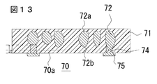
- the mounting substrate 70 shown in FIG. 13 includes a resin layer 71 and a conductor 72 included in the resin layer 71.
- the conductor 72 has, for example, a coil shape made of a series of conductors, and is formed by plating and growing a conductor from the surface opposite to the mounting surface 70a of the resin layer 70 toward the mounting surface 70a.
- the conductor 72 is formed to have a second surface 72b opposite to the first surface 72a, which is the plating growth start surface.
- the conductor 72 is formed between the conductor portions. The distance between the first surface 72a and the second surface 72b is not uniform.
- an object of the present invention is to provide a mounting substrate in which the occurrence of bonding failure in a mounting electrode is suppressed.
- One embodiment of the present invention is a mounting substrate including a resin layer and a first conductor having a contact surface with the resin layer.
- the resin layer has a smooth mounting surface, and the first conductor includes a first surface facing the mounting surface, and a second surface opposite to the first surface. And extending in a direction parallel to the mounting surface.
- the first conductor has a non-uniform thickness in which the distance between the first surface and the second surface varies along the extending direction. In the first conductor, the difference between the maximum value and the minimum value of the distance between the first surface and the mounting surface is greater than the difference between the maximum value and the minimum value of the distance between the second surface and the mounting surface. Is also arranged small.
- the resin layer has a resin wall portion surrounding an opening exposing a part of the first conductor on the mounting surface side, and the exposed portion of the first conductor constitutes a mounting electrode.
- the present invention it is possible to provide a mounting substrate in which the occurrence of bonding failure in the mounting electrode is suppressed.
- sectional drawing of the mounting substrate which concerns on 4th Embodiment It is an example of the end view at the time of planar view of the mounting board
- the mounting substrate of the present embodiment includes a resin layer and a first conductor having a contact surface with the resin layer.
- the resin layer has a mounting surface that is formed smoothly.
- the first conductor has a first surface facing the mounting surface and a second surface opposite to the first surface, and is arranged extending in a direction parallel to the mounting surface.
- the first conductor has a non-uniform thickness in which the distance between the first surface and the second surface varies along the extending direction. In the first conductor, the difference between the maximum value and the minimum value of the distance between the first surface and the mounting surface is greater than the difference between the maximum value and the minimum value of the distance between the second surface and the mounting surface. Is also arranged small.
- the resin layer has a resin wall portion surrounding an opening exposing a part of the first conductor on the mounting surface side, and the exposed portion of the first conductor constitutes a mounting electrode.
- the first conductor is formed with a non-uniform thickness in a direction orthogonal to the mounting surface, but the first surface that is the surface of the first conductor and exposed to the opening is: Since the height difference is smaller than that of the second surface opposite to the first surface, the difference in distance from the mounting surface is small. Therefore, the solder can sufficiently wrap around the entire mounting electrode disposed in the exposed portion of the first conductor during mounting on the substrate, and the occurrence of bonding failure is suppressed. Furthermore, since the difference in distance from the mounting surface between the production lots is also reduced, it can be manufactured efficiently.
- the second surface of the first conductor has a large difference in distance from the mounting surface, and may have a non-planar shape.
- the difference between the maximum value and the minimum value of the distance between the first surface and the mounting surface is calculated by subtracting the minimum value from the maximum value, and the maximum value and the minimum value of the distance between the second surface and the mounting surface are calculated. The difference is the same.
- the first conductor may include a first coil portion that has a winding axis that is orthogonal to the mounting surface and is wound with a resin layer and a contact surface.
- the mounting substrate can be applied to the coil component.
- the average value of the ratio of the thickness in the winding axis direction to the thickness in the width direction orthogonal to the winding axis direction and the winding direction may be 1 or more.
- the conductor portion constituting the first coil portion has a conductor thickness that is a thickness in the winding axis direction and a conductor width that is a width in the direction orthogonal to the winding axis direction in a cross section orthogonal to the winding direction.
- the conductor of the first coil part is formed with an aspect ratio of 1 or more, which is the ratio of the conductor thickness to the conductor width, so that the cross-sectional area of the conductor of the first coil part can be increased while increasing the number of turns of the coil pattern. The conductor loss can be reduced.
- the first conductor can be formed by using an electrolytic plating method, so that the average value of the ratio of the thickness in the winding axis direction to the thickness in the width direction of the conductor can be 1 or more.
- the first conductor is formed using the electrolytic plating method, so that the first conductor is formed with a non-uniform thickness in a direction orthogonal to the mounting surface. For this reason, if the second surface opposite to the first surface of the first conductor is used as a mounting electrode, poor bonding on the mounting surface is likely to occur. In the present embodiment, the occurrence of poor bonding is suppressed by using the exposed portion of the first surface of the first conductor as the mounting electrode.
- the first coil portion may have adjacent conductor portions, and an average value of a ratio of a gap between adjacent conductor portions to a thickness in one winding axis direction of the conductor portion may be 0.5 or less.
- the conductor portions of the conductors formed in series may be formed adjacent to each other.
- the cross-sectional area of the conductor of the first coil portion can be increased while increasing the number of turns of the coil pattern, Conductor loss is reduced.
- the average value of the ratio of the gap between adjacent conductors to the thickness of the conductor can be made 0.5 or less.
- the first conductor When the first conductor is formed using the electrolytic plating method, the first conductor is formed with a non-uniform thickness in a direction orthogonal to the mounting surface. For this reason, if the second surface opposite to the first surface of the first conductor is used as a mounting electrode, poor bonding on the mounting surface is likely to occur. In the present embodiment, the occurrence of poor bonding is suppressed by using the exposed portion of the first surface of the first conductor as the mounting electrode.
- the first surface of the first conductor may be disposed on a surface substantially parallel to the mounting surface. Thereby, the distance between the mounting surface and the mounting electrode becomes more uniform, and the occurrence of poor bonding during mounting is effectively suppressed.
- the first coil portion may have a planar spiral shape.
- the number of coil turns can be increased by adopting a planar spiral shape.
- the planar spiral shape means a shape in which a series of conductors are spirally wound on substantially the same surface and have an inner peripheral portion and an outer peripheral portion. “Substantially on the same plane” means that the spiral shape is not continuously stretched in the winding axis direction.
- the conductor may be spirally wound including a straight portion, or may be spirally wound in a circular or elliptical curve.
- the mounting substrate may further include a second conductor having a resin layer and a contact surface and connected to the first conductor.
- the second conductor has a first surface facing the mounting surface and a second surface opposite to the first surface, and is arranged extending in a direction parallel to the mounting surface, and extending in the extending direction.
- a non-uniform thickness varies along the distance between the first surface and the second surface.
- the difference between the maximum value and the minimum value of the distance between the first surface of the second conductor and the mounting surface is larger than the difference between the maximum value and the minimum value of the distance between the second surface of the second conductor and the mounting surface. It may be arranged small. Since the first surface of the second conductor faces the second surface of the first conductor, the variation in the distance between the first conductor and the second conductor can be reduced. Generation
- the first surface of the second conductor may be disposed on a surface substantially parallel to the mounting surface.
- the second conductor may include a second coil portion that has a winding axis orthogonal to the mounting surface and is wound with the resin layer and the contact surface.
- the mounting substrate can be applied to the coil component, and a greater electromagnetic field strength can be obtained.
- the average value of the ratio of the thickness in the winding axis direction to the thickness in the width direction perpendicular to the winding axis direction and the winding direction may be 1 or more.
- the second coil portion may have adjacent conductor portions, and an average value of a ratio of a gap between adjacent conductor portions to one thickness of the conductor portions may be 0.5 or less.
- the second coil portion may have a planar spiral shape.
- the number of coil turns can be increased by adopting a planar spiral shape.
- the average value of the distance between the mounting surface and the first surface of the first conductor is the minimum value of the distance between the first surface of the first conductor and the second surface of the first conductor. May be smaller. Thereby, the thickness as a whole can be made thin. If the thickness of the mounting substrate is thin, it is easily deformed, but the occurrence of poor bonding on the mounting surface is suppressed.
- An electric element includes a mounting substrate and a support substrate having a connection terminal, and a mounting electrode of the mounting substrate is bonded to the connection terminal of the support substrate via a bonding member.
- a diaphragm according to another embodiment includes a mounting substrate. Thereby, when mounting a diaphragm in a housing
- Another electric element of another embodiment includes a mounting substrate, a housing having a connection terminal, and a magnet, and the mounting electrode of the mounting substrate is bonded to the connection terminal via a bonding member, and the magnet is mounted. It is arranged on the surface side opposite to the mounting surface of the circuit board.
- the mounting electrode of the mounting substrate is bonded to the connection terminal via the bonding member, so that an occurrence of bonding failure is suppressed and an electric element having a good bonding strength between the mounting substrate and the housing is configured. Since the electric element has a magnet arranged to face the mounting substrate, it functions as, for example, a vibration element.
- the mounting substrate manufacturing method includes preparing a resin layer having a base metal layer on at least one surface, forming a resist in a partial region on the base metal layer, First, a metal for forming a conductor is deposited by electrolytic plating in a region where the resist of the layer is not formed, the resist is removed, and a metal is deposited on the formed conductor by electrolytic plating. Forming a conductor, and forming an opening exposing a part of the first conductor on a surface of the resin layer opposite to the surface on which the first conductor is formed. By forming the first conductor by the electrolytic plating method, it is possible to manufacture a mounting board with less conductor loss.
- FIG. 1 is a schematic cross-sectional view of a mounting substrate 10 according to a first embodiment.
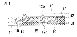
- the mounting substrate 10 includes a resin layer 13 and a first conductor 12, and has an opening 16 that exposes a part of the first conductor 12 on a smooth mounting surface 10a.
- the opening portion 16 is surrounded by the resin wall portion 14, and the exposed portion 15 of the first conductor constitutes a mounting electrode.
- the first conductor 12 has a resin layer 13 and a contact surface.
- the first conductor 12 has a conductor portion that is entirely embedded in the resin layer 13 and a conductor portion that is partially embedded and partially exposed.
- the first conductor 12 has a first surface 12a facing the mounting surface 10a and a second surface 12b opposite to the first surface 12a, and is arranged extending in a direction parallel to the mounting surface 10a. It has a shape.
- the first conductor 12 has a non-uniform thickness in which the distance between the first surface 12a and the second surface 12b varies along the extending direction. For example, in FIG. 1, the thickness in the direction orthogonal to the mounting surface of each conductor portion appearing in the cross section is different depending on each conductor portion. In FIG. 1, the distance between the first surface 12a of the first conductor 12 and the mounting surface 10a is also nonuniform.
- the first conductor 12 has a difference d1 between the maximum value and the minimum value of the distance between the first surface 12a of the first conductor 12 and the mounting surface 10a, and the second surface 12b of the first conductor 12; It is formed smaller than the difference d2 between the maximum value and the minimum value of the distance to the mounting surface 10a.
- d1 is 0 or more and 5 ⁇ m or less
- d2 is, for example, greater than 0 and 10 ⁇ m or less.
- the 1st conductor 12 is formed from metals, such as copper, and the resin layer 14 is formed including at least one of a thermoplastic resin and a thermosetting resin.
- the first conductor 12 constituting the substrate is such that the unevenness difference of the conductor on the first surface 12 a side is smaller than the unevenness difference of the conductor on the second surface 12 b side.
- the difference in the distance between the mounting surface 10a and the exposed portion 15 of the first conductor 12 is small.
- the difference in the distance from the mounting surface 10a to the mounting electrode is reduced between the exposed portions and / or between the manufacturing lots, and the occurrence of bonding failure when mounting the mounting substrate is suppressed.
- the distance between the first surface 12a and the mounting surface 10a in a certain conductor portion is the minimum distance between the mounting surface 10a and the surface parallel to the mounting surface 10a and in contact with the first surface 12a. Measured as a value. Further, the distance between the second surface 12b and the mounting surface 10a in a certain conductor portion is the maximum value of the distance between the mounting surface 10a and the surface parallel to the mounting surface 10a and in contact with the second surface 12b. As measured. Further, the distance between the first surface 12a and the second surface 12b in a conductor portion is such that the surface parallel to the mounting surface 10a and in contact with the first surface 12a, and the second surface 12b parallel to the mounting surface 10a and It is measured as the maximum value of the distance to the contact surface.
- the first conductor having a non-uniform thickness in the direction orthogonal to the mounting surface can be obtained, for example, by forming the first conductor by an electrolytic plating method.
- the first surface of the first conductor has a surface parallel to the mounting surface, and the second surface has a rounded shape.
- Such a first conductor is formed, for example, by plating growth from the mounting surface side toward the surface side opposite to the mounting surface of the resin layer 13.
- d1 may be smaller than d2, and the first surface may be rounded.
- the mounting substrate 10 shown in FIG. 1 can be formed, for example, by growing a conductor on a thermoplastic resin layer and then laminating and pressing the thermoplastic resin on the conductor.
- the substrate can be formed by a simple process, the conductor is displaced in the stacking direction due to the flow of the thermoplastic resin.
- a part of the first conductor 12 is exposed from the resin layer 13, but the entire first conductor 12 may be embedded in the resin layer 13.
- the mounting substrate 10 may have a smooth insulating base layer on the mounting surface.
- the first conductor may include a coil portion having a coil shape.
- the coil shape may be, for example, a planar spiral shape or a so-called meander coil shape.
- FIG. 2 is a schematic cross-sectional view of a mounting board 20 according to a second embodiment.
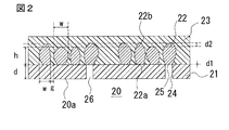
- 2nd Embodiment it comprises similarly to 1st Embodiment except providing the insulating base material layer 21 and the resin layer 23 as a resin layer, and including the 1st conductor 22 in the resin layer 23.
- FIG. 2nd Embodiment comprises similarly to 1st Embodiment except providing the insulating base material layer 21 and the resin layer 23 as a resin layer, and including the 1st conductor 22 in the resin layer 23.
- the mounting substrate 20 includes the insulating base layer 21, the planar spiral first conductor 22 disposed on the insulating base layer 21, and the first conductor 22 disposed on the insulating base layer 21. And the resin layer 23 to be included.
- the mounting substrate 20 has a surface opposite to the resin layer 23 of the insulating base layer 21 as a mounting surface 20a.
- the insulating base material layer 21 has a substantially smooth planar shape with few irregularities on two surfaces orthogonal to the thickness direction.
- the first conductor 22 is arranged in contact with the insulating base material layer 21 on the surface opposite to the mounting surface of the insulating base material layer 21.
- the first conductor 22 is a series of conductors having a planar spiral shape on the insulating base material layer 21 and extending spirally between the inner peripheral portion and the outer peripheral portion.
- the first conductor 22 has a first surface 22a in contact with the insulating base material layer 21, and a second surface 22b opposite to the first surface 22a.
- the distance between the first surface 22a and the second surface 22b of the first conductor 22 changes along the extending and winding direction of the first conductor 22, and the thickness in the direction orthogonal to the mounting surface is formed unevenly. Is done.
- the first conductor 22 is disposed in contact with the flat insulating base material layer 21. Therefore, the distance d 1 between the mounting surface and the first surface 22 a is the entire first conductor 22.
- the first surface 22a of the first conductor 22 is disposed in contact with the smooth insulating base layer 21, the first surface 22a is formed smoothly and substantially parallel to the mounting surface 21a. Placed on a flat surface. As a result, the distance between the mounting surface and the mounting electrode becomes more uniform, the bonding member can sufficiently wrap around the mounting electrode during mounting, and the occurrence of bonding failure is more effectively suppressed.
- the first conductor 22 has a thickness h in a direction perpendicular to the mounting surface and a surface perpendicular to the extending direction of the first conductor 22, for example, a lateral width w in the cross section of FIG. Adjacent conductor portions on the layer 21 are arranged with a gap g.
- the thickness h of the first conductor 22 is measured as a distance between the first surface 22a and the second surface 22b in a certain conductor portion.
- the width w and the gap g are measured as the distance between two surfaces parallel to the winding axis direction and in contact with a certain conductor portion.
- the thickness h of a certain conductor portion is measured as a distance between a surface parallel to the mounting surface 20a and in contact with the first surface 22a and a surface parallel to the mounting surface 20a and in contact with the second surface 22b.
- the width w is measured as a distance between two surfaces that are orthogonal to the mounting surface 20a and parallel to the winding direction, and are in contact with a certain conductor portion.
- the gap g between the conductor portions is two surfaces that are orthogonal to the mounting surface 20a and parallel to the winding direction, and are adjacent to the surfaces of the two conductor portions adjacent to each other on the insulating base layer 21. Measured as the distance between two touching surfaces.
- the thickness h of the first conductor 22 in the winding axis direction is, for example, 30 ⁇ m or more and 45 ⁇ m or less
- the width w is, for example, 25 ⁇ m or more and 45 ⁇ m or less
- the gap g is, for example, 5 ⁇ m or more and 10 ⁇ m or less. It is.
- the thickness h of the first conductor 22 is not a constant value throughout the extending direction of the first conductor 22, and is nonuniform with positions having values different from other positions. Yes. Further, the width w of the first conductor 22 is not constant throughout the extending direction of the first conductor 22, and is nonuniform with positions having values different from other positions.
- the first conductor 22 has an average value of the ratio g / h of the gap g between the adjacent conductor portions to the thickness h of one of the two adjacent conductor portions on the insulating base layer 21, for example, 0. 5 or less, preferably 0.3 or less.
- the thickness h of one of the two conductor portions the larger value of each thickness is used.
- an average value is calculated
- the average value of the ratio h / w of the thickness h to the width w of the first conductor 22 is, for example, 1 or more.
- a coil is formed with a high aspect conductor, so that the number of coil turns per unit area can be increased.
- the average value of the distance d between the mounting surface and the first surface is the distance between the first surface and the second surface, that is, in the direction orthogonal to the mounting surface of the first conductor 22. It is formed smaller than the minimum value of the thickness h. As a result, the entire thickness of the mounting substrate 20 can be reduced.
- the average value of the distance d between the mounting surface and the first surface is obtained as an average value of measured values at arbitrary five locations. In one embodiment of the substrate 20, the average value of the distance d is, for example, 5 ⁇ m or more and 20 ⁇ m or less.
- the first conductor 22 has, for example, a planar spiral shape.
- FIG. 3 is an example of an end view of the interface between the insulating base material layer 21 and the resin layer 23 of the substrate 20 as viewed from the mounting surface side.
- the first conductor 22 is formed by connecting a series of conductors in which an inner peripheral portion and an outer peripheral portion are spirally extended on the surface.
- the planar spiral shape is configured in a rectangular shape that includes straight portions that are orthogonal to each other, and the length of the straight portions changes for each straight line that intersects, but may be formed in a polygonal shape that includes the straight portions. Alternatively, it may be formed to include a curve such as a substantially circular shape or a substantially elliptical shape.
- the first conductor 22 is built in the resin layer 23, but the mounting substrate 20 may not have the resin layer 24.
- the substrate 20 may further include another insulating base material layer on the surface of the resin layer 23 opposite to the surface in contact with the insulating base material layer 21.
- the insulating base layer 21 and the resin layer 24 may be formed of the same material, or may be formed of different materials.
- the insulating base layer may be formed of a thermoplastic resin such as liquid crystal polymer (LCP), or may be formed of a thermosetting resin such as an epoxy resin.
- the resin layer 24 may be formed of a slurry-like insulating resin having fluidity, and the insulating resin may be either a thermoplastic resin or a thermosetting resin.
- the insulating base material layer 21 has an opening 26 in which a part of the first surface which is a contact surface of the first conductor 22 with the insulating base material layer 21 becomes the exposed portion 25.
- the opening 26 is provided in the thickness direction of the insulating base material layer 21 and is surrounded by the resin wall 24.
- the exposed portion 25 of the first conductor 22 in the opening portion 26 constitutes a mounting electrode.
- the mounting electrode may be the exposed portion 25 itself of the first conductor 22, or the exposed surface may be plated with gold, nickel-gold, or the like.
- the mounting electrode is composed of the exposed portion 25 of the first conductor 22, so that the distance between the mounting electrode surface and the mounting surface is formed constant over the entire mounting electrode surface.
- the solder can sufficiently wrap around the mounting electrode, the occurrence of defective bonding is suppressed, and the mounting strength is improved.
- the difference in distance from the mounting surface to the mounting electrode is formed small, the occurrence of poor bonding is suppressed.
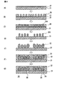
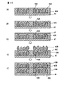
- FIGS. 4A to 4G are schematic views illustrating an example of a manufacturing process of the mounting substrate 20 according to the second embodiment.
- an insulating base material layer 21 having a base metal layer 27 on a surface opposite to a surface to be a mounting surface is prepared.
- the insulating base material layer 21 includes, for example, an insulating thermoplastic resin such as an epoxy resin or a liquid crystal polymer.
- the base metal layer 27 may be formed by laminating a metal foil with the insulating base material layer 21 or may be formed by performing electroless plating on the insulating base material layer 21.
- the base metal layer 27 includes, for example, metallic copper.
- FIG. 4A an insulating base material layer 21 having a base metal layer 27 on a surface opposite to a surface to be a mounting surface is prepared.
- the insulating base material layer 21 includes, for example, an insulating thermoplastic resin such as an epoxy resin or a liquid crystal polymer.
- the base metal layer 27 may be formed by laminating a metal
- a resist 28 serving as a template for the conductor 22A is formed on the base metal layer 27 using, for example, photolithography.
- the resist 28 is formed by exposing the base metal layer 27 in a planar spiral shape.
- the conductor 22A is grown on the base metal layer 27 by electrolytic plating.
- the conductor 22A is formed along the shape of the resist 28.
- the conductor 22A formed by electrolytic plating slightly varies in thickness between adjacent conductors 22A, and the uppermost surface, which is the end of plating growth, forms a curved surface such as an arc.
- the electrolytic plating is performed by depositing metallic copper.
- FIG. 22D the resist 28 is removed.
- the first conductor 22 is formed by further plating and growing the conductor 22A by electrolytic plating. The plating growth is performed, for example, by depositing metallic copper. Since the first conductor 22 is obtained by plating and growing the conductor 22A, the ratio h / w of the thickness h to the width w in the cross section of the first conductor 22 is greater than 1, and the thickness and width are It is formed non-uniformly along the extending direction of one conductor 22.
- an insulating resin layer 23 is disposed on the insulating base material 21 so as to cover the first conductor 22.
- the first conductor 22 is included in the insulating resin layer 23.
- the resin layer 23 includes, for example, a thermosetting resin such as a thermoplastic resin or an epoxy resin.
- a slurry material having fluidity can be used for the formation of the resin layer 23. By using the slurry-like material, the formation of voids between the conductor portions of the first conductor 22 is suppressed, and the resin layer 23 that is leveled on the insulating base layer 21 without gaps can be formed. it can.
- an opening 26 is formed in the insulating base material layer 21 in the thickness direction of the insulating base material layer 21 from the mounting surface side toward the first surface of the first conductor 22.
- a part of 1st surface which is a contact surface with the insulating base material layer 21 of the 1st conductor 22 is exposed, and a mounting electrode is formed.
- the opening 26 is surrounded by the resin wall 24 of the insulating base material layer 21.
- the opening 26 is formed using a laser or the like, for example.
- the mounting substrate 20 is manufactured by the above manufacturing process.
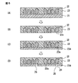
- FIGS. 5A to 5D are schematic views illustrating an example of a manufacturing process of a modified example of the mounting substrate 20 according to the second embodiment.
- a substrate on which the insulating resin layer 23 is laminated is prepared.
- the substrate shown in FIG. 5A can be obtained, for example, by the manufacturing steps shown in FIGS.
- the insulating base material layer 21 is peeled from the resin layer 23. By peeling off the insulating base material layer 21, a substrate including the resin layer 23 and the first conductor 22 having a contact surface with the resin layer 23 is obtained.
- the first surface 22 a of the first conductor 22 is exposed on the mounting surface side surface of the resin layer 23.
- a resist 23A is laminated on the surface of the resin layer 23 on the mounting surface side.
- the resist 23A includes, for example, a thermoplastic resin, a thermosetting resin, or the like.
- the resist 23A may be stacked using the same material as the resin layer 23, or may be stacked using a different material.
- an opening 26 is formed in the thickness direction of the resist 23A from the mounting surface side of the resist 23A toward the first surface 22a of the first conductor 22.
- the opening 26 a part of the first surface 22a of the first conductor 22 is exposed to become an exposed portion 25, which constitutes a mounting electrode.
- the opening 26 is surrounded by the resin wall 24 of the resist 23A.
- FIG. 6 is a schematic cross-sectional view of a mounting board 30 according to a third embodiment.
- the 1st conductor 32 is included in the resin layer 33, the 1st surface of the 1st conductor 32 is arrange
- the difference d1 between the maximum value and the minimum value of the distance between the mounting surface 30a and the first surface 32a is substantially zero.
- plating is grown from the first surface 32 a side of the first conductor 32 to the surface direction opposite to the mounting surface 30 a of the resin layer 33, so that the thickness is not uniform in the direction orthogonal to the mounting surface.
- a first conductor 32 is formed.
- FIG. 7 is a plan view of the mounting board 30 as viewed from the mounting surface 30a side, and is an end view of the surface on which the first surface 32a of the first conductor 32 is disposed.
- the first conductor 32 has a coil portion 32A having a meander coil pattern and a connection portion 32B, and the coil portion 32A and the connection portion 32B are continuously formed by using, for example, an electrolytic plating method.
- FIG. 6 is a cross-sectional view taken along the line aa ′ in FIG. 7.
- FIG. 8 is a schematic cross-sectional view of a mounting board 40 according to a fourth embodiment.
- the mounting substrate 40 in addition to the first conductor 42A, the mounting substrate 40 includes the second conductor 42B disposed on the first resin layer 43A and connected to the first conductor 42A.
- the mounting substrate 20 is the same as the mounting substrate 20 of the second embodiment except that the second resin layer 43B covering the second conductor 42B is provided. Since the mounting substrate 40 according to the fourth embodiment includes a plane spiral conductor in two layers, for example, the electromagnetic field generated by the drive current becomes larger, and the mounting substrate 40 is applied to the vibration plate. Then, a larger driving force can be obtained.
- the mounting substrate 40 is in contact with the insulating base material layer 41, the planar spiral-shaped first conductor 42A disposed on and in contact with the insulating base material layer 41, and the first conductor 42A.
- the first connection conductor 42C that is spaced apart from the first resin layer 43A, the first resin layer 43A that is disposed on the insulating base layer 41 and covers the first conductor 42A and the first connection conductor 43C, and the first resin layer 43A.
- the second conductor 42B connected to the first conductor 42A and the first connection conductor 42C and having a planar spiral shape and the second resin disposed on the first resin layer 43A and covering the second conductor 42B Layer 43B.
- the insulating base material layer 41 has a first surface exposed portion 45A that is a contact surface with the insulating base material layer 41 of the first conductor 42A, and a contact surface of the first connecting conductor 42C with the insulating base material layer 21. And an opening 46 for exposing the exposed portion 45C.
- the opening 46 is provided along the thickness direction of the insulating base material layer 41, and is surrounded by the resin wall portion 44 of the insulating base material layer 41.
- the exposed portion 45A of the first conductor 42A and the exposed portion 45C of the first connection conductor 42C in the opening 46 constitute a mounting electrode.
- the first conductor 42A is plated and grown from the surface side opposite to the mounting surface of the insulating base layer 41 to the surface direction opposite to the mounting surface 40a, and is orthogonal to the mounting surface 40a.
- the first conductor 42A having a non-uniform thickness in the direction is formed.
- the second conductor 42B is disposed on the surface of the first resin layer 43A opposite to the insulating base material layer 41 in contact with the first resin layer 43A.
- the second conductor 42B is connected to the first conductor 42A and the first connection conductor 43C via the second connection conductor 49, respectively.
- the first surface 42Ba of the second conductor 42B is disposed on substantially the same surface, the maximum value of the distance between the mounting surface 40a and the first surface 42Ba of the second conductor 42B.
- the difference d2 between the maximum value and the minimum value of the distance between the mounting surface 40a and the second surface 42Bb of the second conductor 42B is larger than zero.
- the first resin layer 43A is non-uniformly grown in a direction perpendicular to the mounting surface by being plated and grown from the surface opposite to the insulating base layer of the first resin layer 43A to the surface direction opposite to the mounting surface 40a.
- a second conductor 42B having a thickness is formed.
- the second conductor 42B is disposed on the first resin layer 43A, is covered with a second resin layer 43B that covers the second conductor 42B, and is included in the second resin layer 43B.
- the first connection conductor 42 ⁇ / b> C that is disposed on the insulating base material layer 41 and exposes a part of the contact surface with the insulating base material layer 41 in the opening 46 is provided via the second connection conductor 49. It connects with the outer peripheral part of the conductor 42B.
- the inner peripheral portion of the second conductor 42B is connected to the inner peripheral portion of the first conductor 42A through the second connection conductor 49.
- the outer peripheral portion of the first conductor 42A exposes the contact surface 45A with the insulating base material layer at the opening 46.
- a conductor coil in which two planar spiral conductors extending from the first connection conductor 42C to the outer peripheral portion of the first conductor 42A via the second conductor 42B is formed.
- a series of conductor coils may be formed by connecting three or more planar spiral conductors.
- FIG. 9A is an end view when the interface between the first resin layer 43A and the second resin layer 43B of the mounting substrate 40 is viewed from the stacking direction toward the mounting surface, and FIG. It is an end view at the time of seeing the interface of 43 A of 1st resin layers of the board
- the second conductor 42B is formed in a planar spiral shape on the first resin layer 43A.
- 9A shows the shape of the contact surface of the second conductor 42B with the first resin layer 43A.
- the first conductor 42A is formed in a planar spiral shape on the insulating base layer 41, and the first connection conductor 42C is formed at a position corresponding to the end of the outer peripheral portion of the second conductor 42B.
- the shape of the contact surface of the first conductor 42A and the first connection conductor 42C with the insulating base material layer 41 is shown.
- the edge part of the outer peripheral part of the 2nd conductor 42B is connected to 42 C of 1st connection conductors via the 2nd connection conductor arrange
- An end portion of the inner peripheral portion of the second conductor 42B is connected to an end portion of the inner peripheral portion of the first conductor 42A through a second connection conductor disposed in the stacking direction.
- An end portion of the outer peripheral portion of the first conductor 42A and the first connection conductor 42C are exposed at an opening provided in the insulating base material layer 41 to constitute a mounting electrode.
- the first conductor 42A and the second conductor 42B have a planar spiral shape having straight portions, but a planar spiral shape consisting of a circular or elliptical curved portion. You may have done.
- FIGS. 4A to 4F are schematic views showing a manufacturing process of the mounting substrate 40 according to the fourth embodiment.
- the first conductor 42A having a planar spiral shape and the first connection conductor 42C arranged separately from the first conductor 42A, and the first conductor
- the method described in FIGS. 4A to 4F can be applied to the method in which the first conductor 42A and the first connection conductor 42C are disposed on the insulating base layer 41 and covered with the first resin layer 43A. .
- FIG. 4A to 4F can be applied to the method in which the first conductor 42A and the first connection conductor 42C are disposed on the insulating base layer 41 and covered with the first resin layer 43A.
- holes reaching the first conductor 42A and the first connection conductor 42C from the surface of the first resin layer 43A opposite to the insulating base material layer 41 are formed in the stacking direction.
- the hole is formed using, for example, a laser or a drill.
- the base metal layer 47 is formed on the surface of the first resin layer 43A opposite to the insulating base material layer 41.
- a base metal layer is also formed in the hole provided in the first resin layer 43A, and the first conductor 42A and the first connection conductor 42C are connected to the base metal layer 47 on the first resin layer 43A.
- the base metal layer 47 is formed by, for example, electroless plating.
- the second conductor 42B is formed on the base metal layer 47 formed in FIG. 5C in the same manner as the method described with reference to FIGS.
- a second resin layer 43B that covers the second conductor 42B is formed on the first resin layer 43A, and the second conductor 42B is included in the second resin layer 43B.
- Openings are formed in the thickness direction of the insulating base material layer 41 in the insulating base material layer 41 of the obtained laminated body from the mounting surface side toward the first conductor 42A and the first connection conductor 42C. In the opening, a part of the contact surface of the first conductor 42A and the first connection conductor 42C with the insulating base material layer 21 is exposed to form a mounting electrode.
- the mounting substrate 40 as shown in FIG. 8 is manufactured.
- FIG. 11 is a schematic cross-sectional view of an electric element 50 according to a fifth embodiment.
- the electric element 50 includes a mounting substrate 58 according to the fourth embodiment and a support substrate 56 on which the mounting substrate 58 is mounted.
- the support substrate 56 includes a connection terminal 55, and the mounting electrodes 57 ⁇ / b> A and 57 ⁇ / b> C of the mounting substrate 58 are bonded to the connection terminal 55 via the bonding member 54.
- the joining member 54 is formed using, for example, solder.
- the exposed portion of the first surface 52Aa which is the contact surface of the first conductor 52A included in the mounting substrate 58 with the insulating base material layer 51 constitutes the mounting electrode 57A, and the insulating base material of the first connection conductor 52C.
- the first surface, which is the contact surface with the layer 51, constitutes the mounting electrode 57C, so that the occurrence of bonding failure during mounting is suppressed, and the electric element 50 having good bonding strength is formed.
- FIG. 12 is a schematic cross-sectional view of an electric element 60 according to a sixth embodiment.
- the electric element 60 includes a mounting board 68 according to the fourth embodiment, a housing 66 that supports the mounting board 68, and a magnet 69.
- the magnet 69 is disposed on the surface opposite to the mounting surface 68 a of the mounting substrate 68.
- the magnet 69 is disposed to face the first conductor 62A and the second conductor 62B having a planar spiral shape.
- the magnetic flux of the magnet 69 passes in the direction of the spiral winding axis of the first conductor 62A and the second conductor 62B.
- the housing 66 includes a connection terminal 65, and the mounting electrodes 67 ⁇ / b> A and 67 ⁇ / b> C of the mounting substrate 68 are bonded to the connection terminal 65 via the bonding member 64.
- the connection terminal 65 is connected to the circuit of the electronic device.
- a driving current flows through a spiral coil made of a conductor built in the mounting substrate 68 via the mounting electrodes 67A and 67C, the mounting substrate 68 is arranged in the stacking direction of the mounting substrate 68 according to the driving current. Exercise.
- the joining member 64 is formed using, for example, solder.
- An exposed portion of the first surface 62Aa that is a contact surface of the first conductor 62A included in the mounting substrate 68 with the insulating base layer 61 constitutes the mounting electrode 67A, and the insulating base material of the first connection conductor 62C.
- the exposed portion of the first surface, which is the contact surface with the layer 61, constitutes the mounting electrode 67C, so that the occurrence of poor bonding during mounting is suppressed, and the electric element 60 having good bonding strength is formed.
- the magnet 69 is disposed on the surface side opposite to the mounting surface of the mounting substrate 68, but may be disposed on the mounting surface side.
- the distance between the magnet and the region of the planar spiral-shaped first conductor 62A close to the magnet is not affected by the unevenness of the thickness of the first conductor. Variation in characteristics between the two is suppressed.
Landscapes
- Engineering & Computer Science (AREA)
- Power Engineering (AREA)
- Manufacturing & Machinery (AREA)
- Physics & Mathematics (AREA)
- Microelectronics & Electronic Packaging (AREA)
- Acoustics & Sound (AREA)
- Signal Processing (AREA)
- Electromagnetism (AREA)
- Mechanical Engineering (AREA)
- Coils Or Transformers For Communication (AREA)
- Parts Printed On Printed Circuit Boards (AREA)
- Apparatuses For Generation Of Mechanical Vibrations (AREA)
- Manufacturing Cores, Coils, And Magnets (AREA)
Abstract
実装電極における接合不良の発生が抑制される実装用基板が提供される。実装用基板は、樹脂層と、前記樹脂層と接触面を有する第1導電体とを備える。前記樹脂層は、平滑に形成される実装面を有する。前記第1導電体は、前記実装面に対向する第1の面と、前記第1の面と反対側の第2の面とを有し、前記実装面と平行な方向に延伸して配置され、延伸方向に沿って第1の面と第2の面との距離が変化する不均一な厚みを有する。前記第1導電体は、前記第1の面と前記実装面との距離の最大値と最小値の差が、前記第2の面と前記実装面との距離の最大値と最小値の差よりも小さく配置される。前記樹脂層は、前記実装面側に前記第1導電体の一部を露出する開口部を包囲する樹脂壁部を有し、前記第1導電体の露出部が実装電極を構成する。
Description
本発明は、実装用基板に関する。
コイル部品の構造としてプリント回路基板技術を応用した平面コイル構造が知られている。例えば特開2012-248630号公報には、基板の両面に電解めっきによって形成された平面スパイラル導体を含むコイル部品が記載されている。
電解めっきによって平面スパイラル導体を厚く形成すると、電解めっきによる導体の成長速度にばらつきが生じやすいため、形成される平面スパイラル導体の膜厚が不均一になる場合がある。加えて平面スパイラル導体の端部に、端部と連続して形成される引出導体を電解めっきにより形成して実装電極とする場合には、実装電極の膜厚が不均一になる。このような平面スパイラル導体または実装電極を有するコイル部品を、実装基板上に接合する場合、不均一に形成される導体形状に起因する接合不良が発生するという課題がある。例えば図13に示す実装用基板70は、樹脂層71と樹脂層71に内包される導電体72とを備える。導電体72は例えば一連の導体からなるコイル形状を有し、樹脂層70の実装面70aとは反対の面側から実装面70a方向に導体をめっき成長させることで形成される。導電体72はめっき成長の開始面である第1の面72aと反対側の第2の面72bを有して形成されるが、電解めっきによる導体の成長速度のばらつきにより、導体部分間で第1の面72aと第2の面72bとの距離が不均一になっている。そのため、実装用基板70のように、実装面70aを樹脂層71の第2の面72b側として実装面側に開口部を設けて実装電極を形成すると、実装面70aと実装電極との距離の差が、導体部分間で大きくなる。その結果、実装用基板70を接続端子75に接合部材74を用いて接合する際に、接合不良が発生し易くなる。上記課題に鑑み、本発明は、実装電極における接合不良の発生が抑制される実装用基板を提供することを課題とする。
本発明の一実施形態は、樹脂層と、前記樹脂層と接触面を有する第1導電体とを備える実装用基板である。前記樹脂層は、平滑に形成される実装面を有し、前記第1導電体は、前記実装面に対向する第1の面と、前記第1の面と反対側の第2の面とを有し、前記実装面と平行な方向に延伸して配置される。前記第1導電体は、延伸方向に沿って第1の面と第2の面との距離が変化する不均一な厚みを有する。前記第1導電体は、前記第1の面と前記実装面との距離の最大値と最小値の差が、前記第2の面と前記実装面との距離の最大値と最小値の差よりも小さく配置される。前記樹脂層は、前記実装面側に前記第1導電体の一部を露出する開口部を包囲する樹脂壁部を有し、前記第1導電体の露出部が実装電極を構成する。
本発明によれば、実装電極における接合不良の発生が抑制される実装用基板を提供することができる。
本実施形態の実装用基板は、樹脂層と、前記樹脂層と接触面を有する第1導電体とを備える。前記樹脂層は、平滑に形成される実装面を有する。前記第1導電体は、前記実装面に対向する第1の面と、前記第1の面と反対側の第2の面とを有し、前記実装面と平行な方向に延伸して配置される。前記第1導電体は、延伸方向に沿って第1の面と第2の面との距離が変化する不均一な厚みを有する。前記第1導電体は、前記第1の面と前記実装面との距離の最大値と最小値の差が、前記第2の面と前記実装面との距離の最大値と最小値の差よりも小さく配置される。前記樹脂層は、前記実装面側に前記第1導電体の一部を露出する開口部を包囲する樹脂壁部を有し、前記第1導電体の露出部が実装電極を構成する。
第1導電体は実装面と直交する方向に不均一な厚みを有して形成されるが、第1導電体の面であって開口部に露出する側の面である第1の面は、第1の面とは反対側の第2の面よりも高低差が小さく形成されているので、実装面との距離の差が小さくなっている。そのため、基板への実装の際に第1導電体の露出部に配置される実装電極全体に、はんだが十分に回り込むことができ、接合不良の発生が抑制される。さらに製造ロット間での実装面との距離の差も小さくなるため、効率的に製造することができる。一方、第1導電体の第2の面は、実装面からの距離の差が大きくなっており、非平面形状をなす場合がある。そのため第2の面側に実装電極を配置すると、実装電極におけるはんだの回り込み不良が発生し易くなり、接合不良の発生率が上昇する場合がある。なお、第1の面と実装面との距離の最大値と最小値の差は、最大値から最小値を差し引いて算出され、第2の面と実装面との距離の最大値と最小値の差も同様である。
第1導電体は、実装面と直交する巻軸を有し、樹脂層と接触面を有して巻回される第1コイル部を含んでいてもよい。第1導電体が第1コイル部を含むことで実装用基板をコイル部品に適用することができる。
第1コイル部は、巻軸方向および巻回し方向に直交する幅方向の厚みに対する巻軸方向の厚みの比の平均値が1以上であってもよい。第1コイル部を構成する導体部分は、巻回し方向に直交する断面において巻軸方向の厚みである導体厚みと、巻軸方向に直交する方向の幅である導体幅とを有する。第1コイル部の導体が、導体幅に対する導体厚みの比であるアスペクト比が1以上で形成されていることで、コイルパターンの巻数をより多くしつつ、第1コイル部の導体の断面積を大きくすることができ、導体損失が低減される。第1導電体は例えば、電解めっき工法を用いて形成されることで、導電体の幅方向の厚みに対する巻軸方向の厚みの比の平均値を1以上にすることができる。電解めっき工法を用いて第1導電体を形成すると、第1導電体は実装面と直交する方向に不均一な厚みを有して形成される。そのため、第1導電体の第1の面とは反対側の第2の面を実装電極とすると、実装面における接合不良が発生し易くなる。本実施形態では、第1導電体の第1の面の露出部を実装電極とすることで接合不良の発生が抑制される。
第1コイル部は、隣接する導電体部分を有し、導電体部分の一方の巻軸方向の厚みに対する隣接する導電体部分間の間隙の比の平均値が0.5以下であってもよい。第1コイル部では一連に形成される導体の導体部分どうしが互いに隣接して形成されている場合がある。導体の巻軸方向の厚みを厚く、また隣接する導体部分間の間隙を小さくすることで、コイルパターンの巻数をより多くしつつ、第1コイル部の導体の断面積を大きくすることができ、導体損失が低減される。第1導電体は例えば、電解めっき工法を用いて形成されることで、導電体の厚みに対する隣接する導電体間の間隙の比の平均値を0.5以下にすることができる。電解めっき工法を用いて第1導電体を形成すると、第1導電体は実装面と直交する方向に不均一な厚みを有して形成される。そのため、第1導電体の第1の面とは反対側の第2の面を実装電極とすると、実装面における接合不良が発生し易くなる。本実施形態では、第1導電体の第1の面の露出部を実装電極とすることで接合不良の発生が抑制される。
第1導電体の第1の面は、実装面に略平行な面上に配置されていてもよい。これにより、実装面と実装電極との距離がより均一になり、実装時における接合不良の発生が効果的に抑制される。
第1コイル部は、平面スパイラル形状を有していてもよい。平面スパイラル形状とすることでコイル巻数を増やすことができる。ここで平面スパイラル形状とは、一連の導電体が、実質的に同一面上で螺旋状に巻回されて形成され、内周部と外周部とを有する形状を意味する。実質的に同一面上とは、スパイラル形状が巻軸方向に連続的に延伸していないことを意味する。平面スパイラル形状では、導電体が直線部を含んで螺旋状に巻回されていてもよく、円形又は楕円形様の曲線をなして螺旋状に巻回されてもよい。
実装用基板は、樹脂層と接触面を有し、第1導電体と接続される第2導電体を更に備えていてもよい。第2導電体は、実装面に対向する第1の面と、第1の面と反対側の第2の面とを有し、実装面と平行な方向に延伸して配置され、延伸方向に沿って第1の面と第2の面との距離が変化する不均一な厚みを有する。導電体が複数層に渡って配置されることで、実装基板を例えば、コイル部品に使用する場合に駆動電流によって発生する電磁界の強度をより大きくすることができる。
第2導電体の第1の面と実装面との距離の最大値と最小値の差が、第2導電体の第2の面と実装面との距離の最大値と最小値の差よりも小さく配置されていてもよい。第2導電体の第1の面が、第1導電体の第2の面と対向することで、第1導電体と第2導電体との間の距離の変動を少なくすることができ、第1導電体と第2導電体の接続部における接合不良の発生が抑制できる。
第2導電体の前記第1の面は、前記実装面に略平行な面上に配置されていてもよい。これにより、第1導電体と第2導電体の接続部における接合不良の発生がより効果的に抑制される。
第2導電体は、実装面と直交する巻軸を有し、樹脂層と接触面を有して巻回される第2コイル部を含んでもよい。第2導電体が第2コイル部を含むことで実装用基板をコイル部品に適用することができ、より大きな電磁界の強度を得ることができる。
第2コイル部は、前記巻軸方向および巻回し方向に直交する幅方向の厚みに対する巻軸方向の厚みの比の平均値が1以上であってもよい。これによりコイルパターンの巻数をより多くしつつ、第1コイル部の導体の断面積を大きくすることができ、導体損失が低減される。
第2コイル部は、隣接する導電体部分を有し、前記導電体部分の一方の厚みに対する隣接する導電体部分間の間隙の比の平均値が0.5以下であってもよい。これによりコイルパターンの巻数をより多くしつつ、第1コイル部の導体の断面積を大きくすることができ、導体損失が低減される。
第2コイル部は、平面スパイラル形状を有していてもよい。平面スパイラル形状とすることでコイル巻数を増やすことができる。
実装用基板は、実装面と第1導電体の第1の面との距離の平均値が、第1導電体の第1の面と第1導電体の第2の面との距離の最小値よりも小さくてもよい。これにより全体としての厚みを薄くすることができる。実装用基板としての厚みが薄いと容易に変形するが、実装面における接合不良の発生は抑制される。
別の実施形態である電気素子は、実装用基板と、接続端子を有する支持基板とを備え、前記実装用基板の実装電極が前記支持基板の接続端子に接合部材を介して接合される。実装用基板を用いることで、電気素子を形成する場合に接合不良の発生を抑制できる。また実装用基板と支持基板との接合強度が良好な電気素子が構成される。
別の実施形態である振動板は、実装用基板を含んで構成される。これにより振動板を筐体等に実装する場合に、接合不良の発生を抑制できる。
別の実施形態の他の電気素子は、実装用基板と、接続端子を有する筐体と、磁石とを備え、実装用基板の実装電極が接続端子に接合部材を介して接合され、磁石が実装用基板の実装面とは反対の面側に配置されてなる。実装用基板の実装電極が接続端子に接合部材を介して接合されることで、接合不良の発生が抑制され、実装用基板と筐体との接合強度が良好な電気素子が構成される。電気素子は実装用基板に対向して配置される磁石を有することから、例えば、振動素子として機能する。
本実施形態の実装用基板の製造方法は、少なくとも一方の面上に下地金属層を有する樹脂層を準備することと、下地金属層上の一部の領域にレジストを形成することと、下地金属層のレジストが形成されていない領域に、電解めっきにより導電体を形成する金属を析出させることと、レジストを除去することと、形成された導電体に、電解めっきにより金属を析出させて第1導電体を形成することと、樹脂層の前記第1導電体が形成される面とは反対側の面に、第1導電体の一部を露出する開口部を形成することと、を含む。第1導電体を電解めっき工法により形成することで、導体損失の少ない実装用基板を製造することができる。
以下、本発明の実施形態を図面に基づいて説明する。ただし、以下に示す実施形態は、本発明の技術思想を具体化するための、電気素子を例示するものであって、本発明は、電気素子を以下のものに限定しない。なお特許請求の範囲に示される部材を、実施形態の部材に限定するものでは決してない。特に実施形態に記載されている構成部品の寸法、材質、形状、その相対的配置等は特に特定的な記載がない限りは、本発明の範囲をそれのみに限定する趣旨ではなく、単なる説明例にすぎない。なお、各図中には同一箇所に同一符号を付している。要点の説明または理解の容易性を考慮して、便宜上実施形態を分けて示すが、異なる実施形態で示した構成の部分的な置換または組み合わせが可能である。第2実施形態以降では第1実施形態と共通の事柄についての記述を省略し、異なる点についてのみ説明する。特に、同様の構成による同様の作用効果については実施形態毎には逐次言及しない。
第1実施形態
図1は、第1実施形態に係る実装用基板10の概略断面図である。実装用基板10は、樹脂層13と第1導電体12とを備え、平滑に形成される実装面10aに第1導電体12の一部を露出する開口部16を有している。開口部16は樹脂壁部14で包囲され、第1導電体の露出部15が実装電極を構成する。実装用基板10では、第1導電体12が樹脂層13と接触面を有している。図1では第1導電体12は、樹脂層13に全体が埋設される導電体部分と、一部が埋設され、一部が露出する導電体部分とを有している。第1導電体12は、実装面10aに対向する第1の面12aとその反対側の第2の面12bとを有し、実装面10aと平行な方向に延伸して配置され、例えば、コイル形状を有している。また第1導電体12は延伸方向に沿って第1の面12aと第2の面12bとの距離が変化する不均一な厚みを有している。例えば図1では、断面に現れる各導電体部分の実装面に直交する方向の厚みが、各導電体部分によって異なる厚みとなっている。また図1では、第1導電体12の第1の面12aと、実装面10aとの距離も不均一になっている。第1導電体12は、第1導電体12の第1の面12aと、実装面10aとの距離の最大値と最小値の差d1が、第1導電体12の第2の面12bと、実装面10aとの距離の最大値と最小値の差d2よりも小さく形成される。d1は例えば、0以上5μm以下であり、d2は例えば、0より大きく10μm以下である。第1導電体12は、銅等の金属から形成され、樹脂層14は、熱可塑性樹脂および熱硬化性樹脂の少なくとも一方を含んで形成される。
図1は、第1実施形態に係る実装用基板10の概略断面図である。実装用基板10は、樹脂層13と第1導電体12とを備え、平滑に形成される実装面10aに第1導電体12の一部を露出する開口部16を有している。開口部16は樹脂壁部14で包囲され、第1導電体の露出部15が実装電極を構成する。実装用基板10では、第1導電体12が樹脂層13と接触面を有している。図1では第1導電体12は、樹脂層13に全体が埋設される導電体部分と、一部が埋設され、一部が露出する導電体部分とを有している。第1導電体12は、実装面10aに対向する第1の面12aとその反対側の第2の面12bとを有し、実装面10aと平行な方向に延伸して配置され、例えば、コイル形状を有している。また第1導電体12は延伸方向に沿って第1の面12aと第2の面12bとの距離が変化する不均一な厚みを有している。例えば図1では、断面に現れる各導電体部分の実装面に直交する方向の厚みが、各導電体部分によって異なる厚みとなっている。また図1では、第1導電体12の第1の面12aと、実装面10aとの距離も不均一になっている。第1導電体12は、第1導電体12の第1の面12aと、実装面10aとの距離の最大値と最小値の差d1が、第1導電体12の第2の面12bと、実装面10aとの距離の最大値と最小値の差d2よりも小さく形成される。d1は例えば、0以上5μm以下であり、d2は例えば、0より大きく10μm以下である。第1導電体12は、銅等の金属から形成され、樹脂層14は、熱可塑性樹脂および熱硬化性樹脂の少なくとも一方を含んで形成される。
実装用基板10では、基板を構成する第1導電体12が、第1の面12a側における導電体の凹凸差が、第2の面12b側における導電体の凹凸差よりも小さくなっていることで、実装面10aと第1導電体12の露出部15との距離の差が小さくなっている。これにより、実装面10aから実装電極までの距離の差が、露出部間および/または製造ロット間で小さくなり、実装用基板を実装する際の接合不良の発生が抑制される。
ここで、ある導電体部分における第1の面12aと実装面10aとの距離は、実装面10aに平行な面であって第1の面12aと接する面と、実装面10aとの距離の最小値として測定される。また、ある導電体部分における第2の面12bと実装面10aとの距離は、実装面10aに平行な面であって第2の面12bと接する面と、実装面10aとの距離の最大値として測定される。更にある導電体部分における第1の面12aと第2の面12bとの距離は、実装面10aに平行で第1の面12aと接する面と、実装面10aに平行で第2の面12bと接する面との距離の最大値として測定される。
実装面に直交する方向の厚みが不均一な第1導電体は例えば、電解めっき工法で第1導電体を形成することで得られる。図1では、第1導電体の第1の面が実装面に平行な面を有しており、第2の面が丸みを帯びた形状をなしている。このような第1導電体は例えば、実装面側から、樹脂層13の実装面とは反対側の面側に向かってめっき成長させることで形成される。本実施形態では、d1がd2よりも小さくなっていればよく、第1の面が丸みを帯びた形状であってもよい。図1に示される実装用基板10は、例えば、熱可塑性樹脂層上で導電体をめっき成長させた後、導電体上に熱可塑性樹脂を積層して一括プレスすることで形成することができる。簡易な工程で基板を形成できる一方、その際に熱可塑性樹脂の流動により導電体が積層方向に位置ずれしている。図1では、第1導電体12の一部が樹脂層13から露出しているが、第1導電体12の全体が樹脂層13に内蔵されていてもよい。また実装用基板10は実装面上に、平滑な絶縁基材層を有していてもよい。また第1導電体はコイル形状を有するコイル部を含んでいてもよい。第1導電体12がコイル部を有する場合、そのコイル形状は例えば、平面スパイラル形状であってもよく、いわゆるミアンダコイル形状であってもよい。
第2実施形態
図2は、第2実施形態に係る実装用基板20の概略断面図である。第2実施形態では、樹脂層として絶縁基材層21および樹脂層23を備えること、第1導電体22が樹脂層23に内包されること以外は、第1実施形態と同様に構成される。
図2は、第2実施形態に係る実装用基板20の概略断面図である。第2実施形態では、樹脂層として絶縁基材層21および樹脂層23を備えること、第1導電体22が樹脂層23に内包されること以外は、第1実施形態と同様に構成される。
実装用基板20は、絶縁基材層21と、絶縁基材層21上に配置される平面スパイラル形状の第1導電体22と、絶縁基材層21上に配置され第1導電体22を内包する樹脂層23とを含む。実装用基板20は絶縁基材層21の樹脂層23とは反対側の面を実装面20aとして構成される。絶縁基材層21は、厚み方向に直交する2つの面が凹凸の少ない略平滑な平面形状をなしている。第1導電体22は、絶縁基材層21の実装面とは反対側の面上に絶縁基材層21と接して配置される。第1導電体22は、絶縁基材層21上で平面スパイラル形状を有し、内周部と外周部との間に螺旋状に延伸されてなる一連の導電体である。また第1導電体22は絶縁基材層21に接する第1の面22aと、第1の面22aとは反対側の第2の面22bとを有する。第1導電体22の第1の面22aと第2の面22bとの距離は第1導電体22の延伸巻回し方向に沿って変化し、実装面に直交する方向の厚みが不均一に形成される。実装用基板20では、第1導電体22が、平板状の絶縁基材層21に接して配置されるため、実装面と第1の面22aとの距離d1は、第1導電体22の全体についてほぼ一定となっている。そのため実装面と第1の面との距離の最大値と最小値の差はほぼ0になっている。一方、実装面と第2の面22bとの距離は、第1導電体22の延伸方向に沿って変化し、不均一になっている。そのためd2は0より大きくなっている。すなわち、実装面20aと第1の面22aとの距離の最大値と最小値の差d1が、実装面20aと第2の面22bとの距離の最大値と最小値の差d2よりも小さくなっている。また図2では、第1導電体22の第1の面22aが、平滑な絶縁基材層21に接して配置されるため、第1の面22aが平滑に形成され、実装面21aに略平行な面上に配置される。これにより、実装面と実装電極との距離がより均一になり、実装時において接合部材が、実装電極に充分に回り込むことができ、接合不良の発生がより効果的に抑制される。
第1導電体22は、実装面と直交する方向の厚みhと、第1導電体22の延伸方向に直交する面、例えば図2の断面における横方向の幅wとを有し、絶縁基材層21上で隣接する導電体部分が間隙gを有して配置される。ここで第1導電体22の厚みhは、ある導電体部分における第1の面22aと第2の面22bとの距離として計測される。幅w及び間隙gは、巻軸方向に平行で、ある導電体部分に接する2つ面の間の距離として計測される。具体的には、ある導電体部分の厚みhは、実装面20aに平行で第1の面22aと接する面と、実装面20aに平行で第2の面22bと接する面との距離として測定される。また幅wは、実装面20aと直交し、巻回し方向に平行な2つの面であって、ある導電体部分と接する2つの面の間の距離として測定される。導電体部分間の間隙gは、実装面20aと直交し、巻回し方向に平行な2つの面であって、絶縁基材層21上で隣接する2つの導電体部分の互いに対向する面にそれぞれ接する2つの面の間の距離として測定される。
基板29の一態様において、第1導電体22の巻軸方向の厚みhは例えば、30μm以上45μm以下であり、幅wは例えば、25μm以上45μm以下であり、間隙gは例えば、5μm以上10μm以下である。
図2では、第1導電体22の厚みhは、第1導電体22の延伸方向の全体を通して一定の値ではなく、他の位置とは異なる値を有する位置を有して不均一になっている。また第1導電体22の幅wは、第1導電体22の延伸方向の全体を通して一定の値ではなく、他の位置とは異なる値を有する位置を有して不均一になっている。
第1導電体22は、絶縁基材層21上で隣接する2つの導電体部分の一方の厚みhに対する、隣接する導電体部分間の間隙gの比g/hの平均値が、例えば0.5以下であり、好ましくは0.3以下になっている。ここで、2つの導電体部分の一方の厚みhとしては、それぞれの厚みのうち大きい方の値を用いる。また平均値は、任意の5カ所について算出される比の平均値として求める。比g/hの平均値が所定値以下であると、導電体が狭ギャップでコイルが形成されるため、単位面積当たりのコイル巻数を多くすることができる。
第1導電体22は、幅wに対する厚みhの比h/wの平均値が、例えば1以上である。比h/wの平均値が所定値以上であると、高アスペクトの導電体でコイルが形成されるため、単位面積当たりのコイル巻数を多くすることができる。
実装用基板20では、実装面と第1の面との距離dの平均値が、第1の面と第2の面との距離、すなわち、第1導電体22の実装面と直交する方向の厚みhの最小値よりも小さく形成されている。これにより実装用基板20の全体としての厚みを薄く形成することができる。なお、実装面と第1の面との距離dの平均値は、任意の5カ所についての測定値の平均値として求める。基板20の一態様において、距離dの平均値は例えば、5μm以上20μm以下である。
第1導電体22は例えば、平面スパイラル形状を有している。図3は、基板20の絶縁基材層21と樹脂層23との界面を実装面側から見た端面図の一例である。図3では、第1導電体22が、内周部と外周部とが面上で螺旋状に延伸して配置される一連の導電体で接続されて形成されている。図3では平面スパイラル形状が、直交する直線部を含んで直線部の長さが交差する直線毎に変化する矩形状に構成されているが、直線部を含む多角形状に形成されていてもよく、略円形、略楕円形等の曲線を含んで形成されていてもよい。
図2では、第1導電体22が樹脂層23に内蔵されているが、実装用基板20は樹脂層24を有していなくてもよい。また、基板20は樹脂層23の絶縁基材層21と接する面とは反対側の面上に他の絶縁基材層をさらに備えるものであってもよい。絶縁基材層21と樹脂層24とは同じ材料で形成されていてもよく、異なる材料で形成されてもよい。絶縁基材層は例えば、液晶ポリマー(LCP)等の熱可塑樹脂で形成されてもよく、エポキシ樹脂等の熱硬化性樹脂で形成されてよい。樹脂層24は例えば、流動性を有するスラリー状の絶縁性樹脂で形成されてもよく、絶縁性樹脂は熱可塑樹脂および熱硬化性樹脂のいずれであってもよい。樹脂層23を流動性を有するスラリー状の絶縁性樹脂で形成することにより、第1導電体22が積層方向に位置ずれを起こすことなく、第1の面22aが略同一面上に配置される。
絶縁基材層21は、第1導電体22の絶縁基材層21との接触面である第1の面の一部が露出部25となる開口部26を有する。開口部26は絶縁基材層21の厚み方向に設けられ、樹脂壁部24に包囲されている。開口部26における第1導電体22の露出部25は実装電極を構成する。実装電極は第1導電体22の露出部25自体であってもよいし、露出している面が、金、ニッケル-金等でめっき処理されたものであってもよい。
実装用基板20では、実装電極が第1導電体22の露出部25で構成されることで、実装電極の面と実装面との距離が、実装電極の面全体について一定に形成される。これにより実装電極にはんだが十分に回り込むことができ、接合不良の発生が抑制され、また実装強度が向上する。また、実装面から実装電極までの距離の差が小さく形成されるので接合不良の発生が抑制される。
図4(A)から(G)は、第2実施形態に係る実装用基板20の製造工程の一例を示す概略図である。図4(A)では実装面となる面とは反対側の面上に下地金属層27を有する絶縁基材層21を準備する。絶縁基材層21は、例えば、エポキシ樹脂、液晶ポリマー等の絶縁性の熱可塑性樹脂を含む。下地金属層27は、金属箔を絶縁基材層21と積層して形成されてもよく、絶縁基材層21に無電解めっきを施して形成されてもよい。下地金属層27は例えば、金属銅を含む。図4(B)では下地金属層27上に、導電体22Aの鋳型となるレジスト28を、例えばフォトリソグラフィーを用いて形成する。レジスト28は平面スパイラル形状に下地金属層27を露出して形成される。図4(C)では電解めっきにより、下地金属層27上に導電体22Aをめっき成長させる。導電体22Aはレジスト28の形状に沿って形成される。電解めっきによって形成される導電体22Aは、その厚みが隣接する導電体22A間でわずかに変動し、めっき成長の端部である最上面が円弧状等の曲面をなす。電解めっきは例えば、金属銅を析出させて行われる。図22(D)ではレジスト28を除去する。レジスト28の除去に際しては、下地金属層27のレジスト28で被覆された部分も同時に除去し、導電体22Aの間に絶縁基材層21を露出させる。下地金属層27の除去はエッチングで行ってもよい。図4(E)では電解めっきにより、導電体22Aをさらにめっき成長させて第1導電体22を形成する。めっき成長は例えば、金属銅を析出させて行われる。第1導電体22は導電体22Aをめっき成長させて得られるため、第1導電体22の断面における幅wに対する厚みhの比h/wが1よりも大きくなり、また厚み及び幅が、第1導電体22の延伸方向に沿って、不均一に形成される。まためっき成長して形成される第1導電体22においては、隣接する導電体間の間隙がめっき成長前に比べて狭くなる。図4(F)では絶縁基材21上に絶縁性の樹脂層23を、第1導電体22を被覆して配置する。第1導電体22は絶縁性の樹脂層23に内包される。樹脂層23は、例えば、熱可塑性樹脂、エポキシ樹脂等の熱硬化性樹脂を含む。樹脂層23の形成には、流動性を有するスラリー状の材料を用いることができる。スラリー状の材料を用いることで、第1導電体22の導電体部分間に空隙が形成されることが抑制され、絶縁基材層21上に隙間なくレベリングされた樹脂層23を形成することができる。さらに絶縁基材層21の変形により第1導電体22が実装面側に不均一に突出することが抑制される。図4(G)では、絶縁基材層21に実装面側から第1導電体22の第1の面に向けて、絶縁基材層21の厚み方向に開口部26が形成される。開口部26では第1導電体22の絶縁基材層21との接触面である第1の面の一部が露出して実装電極を形成する。開口部26は絶縁基材層21の樹脂壁部24で包囲されている。開口部26は例えば、レーザー等を用いて形成される。以上の製造工程により、実装用基板20が製造される。
図5(A)から(D)は、第2実施形態に係る実装用基板20の変形例の製造工程の一例を示す概略図である。図5(A)では、絶縁基材層21と、絶縁基材層21と接触して配置される第1導電体22と、絶縁基材層21の第1導電体22が配置される面上に絶縁性の樹脂層23が積層して配置される基板を準備する。図5(A)の基板は例えば、図4(A)から(F)の製造工程で得ることができる。図5(B)では、樹脂層23から絶縁基材層21を剥離する。絶縁基材層21が剥離されることで、樹脂層23および樹脂層23と接触面を有する第1導電体22を含む基板が得られる。図5(B)の基板では、第1導電体22の第1の面22aが樹脂層23の実装面側の面上に露出している。図5(C)では、樹脂層23の実装面側の面上にレジスト23Aを積層する。レジスト23Aは例えば、熱可塑性樹脂、熱硬化性樹脂等を含んで構成される。レジスト23Aは樹脂層23と同じ材料を用いて積層されてもよく、異なる材料を用いて積層されてもよい。レジスト23Aを樹脂層23の実装面側に配置することで第1導電体22の第1の面22aが絶縁被覆される。また、レジスト23Aの樹脂層23とは反対側の面は、平滑に形成されて実装面となる。図5(D)では、レジスト23Aの実装面側から第1導電体22の第1の面22aに向けて、レジスト23Aの厚み方向に開口部26が形成される。開口部26では第1導電体22の第1の面22aの一部が露出して露出部25となり、実装電極を構成する。開口部26はレジスト23Aの樹脂壁部24で包囲されている
第3実施形態
図6は、第3実施形態に係る実装用基板30の概略断面図である。第3実施形態では、第1導電体32が樹脂層33中に内包されていること、第1導電体32の第1の面が略同一面上に配置されていること、第1導電体が第1コイル部32aと、第1コイル部から連続して形成される接続部32bとを有し、接続部32bに実装電極を有することを以外は、第1実施形態と同様に構成される。図6では、第1導電体32の第1の面が略同一面上に配置されているため、実装面30aと第1の面32aとの距離の最大値と最小値の差d1がほぼ0になっているが、実装面30aと第2の面32bとの距離の最大値と最小値の差d2は0より大きくなっている。図6では、第1導電体32の第1の面32a側から、樹脂層33の実装面30aとは反対側の面方向にめっき成長させて、実装面と直交する方向に不均一な厚みを有する第1導電体32が形成される。
図6は、第3実施形態に係る実装用基板30の概略断面図である。第3実施形態では、第1導電体32が樹脂層33中に内包されていること、第1導電体32の第1の面が略同一面上に配置されていること、第1導電体が第1コイル部32aと、第1コイル部から連続して形成される接続部32bとを有し、接続部32bに実装電極を有することを以外は、第1実施形態と同様に構成される。図6では、第1導電体32の第1の面が略同一面上に配置されているため、実装面30aと第1の面32aとの距離の最大値と最小値の差d1がほぼ0になっているが、実装面30aと第2の面32bとの距離の最大値と最小値の差d2は0より大きくなっている。図6では、第1導電体32の第1の面32a側から、樹脂層33の実装面30aとは反対側の面方向にめっき成長させて、実装面と直交する方向に不均一な厚みを有する第1導電体32が形成される。
図7は、実装基板30を実装面30a側から見た平面図であり、第1導電体32の第1の面32aが配置される面における端面図である。第1導電体32はミアンダコイルパターンを有するコイル部32Aと接続部32Bとを有し、コイル部32Aと接続部32Bとは例えば、電解めっき工法を用いて連続して形成されている。なお、図7におけるaa’切断線における断面図が図6に該当する。
第4実施形態
図8は、第4実施形態に係る実装用基板40の概略断面図である。第4実施形態に係る実装用基板40では、第1導電体42Aに加えて、第1樹脂層43A上に配置され、第1導電体42Aと接続する第2導電体42Bを有することと、絶縁基材41上に接触して配置され、第2導電体42Bと接続し、絶縁基材41との接触面を開口部46に露出する第1接続導体42Cと、第1樹脂層43A上に配置され第2導電体42Bを被覆する第2樹脂層43Bを有することを除いて第2実施形態の実装用基板20と同様に構成される。第4実施形態に係る実装用基板40では、平面スパイラル形状の導電体を2層に渡って含むため、例えば、駆動電流によって発生する電磁界がより大きくなり、実装用基板40を振動版に適用すると、より大きな駆動力を得ることができる。
図8は、第4実施形態に係る実装用基板40の概略断面図である。第4実施形態に係る実装用基板40では、第1導電体42Aに加えて、第1樹脂層43A上に配置され、第1導電体42Aと接続する第2導電体42Bを有することと、絶縁基材41上に接触して配置され、第2導電体42Bと接続し、絶縁基材41との接触面を開口部46に露出する第1接続導体42Cと、第1樹脂層43A上に配置され第2導電体42Bを被覆する第2樹脂層43Bを有することを除いて第2実施形態の実装用基板20と同様に構成される。第4実施形態に係る実装用基板40では、平面スパイラル形状の導電体を2層に渡って含むため、例えば、駆動電流によって発生する電磁界がより大きくなり、実装用基板40を振動版に適用すると、より大きな駆動力を得ることができる。
実装用基板40は、絶縁基材層41と、絶縁基材層41上に接して配置される平面スパイラル形状の第1導電体42Aと、絶縁基材層41上に接し、第1導電体42Aと離隔して配置される第1接続導体42Cと、絶縁基材層41上に配置され第1導電体42A及び第1接続導体43Cを被覆する第1樹脂層43Aと、第1樹脂層43A上に配置され第1導電体42A及び第1接続導体42Cと接続し、平面スパイラル形状を有する第2導電体42Bと、第1樹脂層43A上に配置され第2導電体42Bを被覆する第2樹脂層43Bとを有する。絶縁基材層41には、第1導電体42Aの絶縁基材層41との接触面である第1の面の露出部45Aと、第1接続導体42Cの絶縁基材層21との接触面である露出部45Cとを露出する開口部46を有する。開口部46は絶縁基材層41の厚み方向に沿って設けられ、絶縁基材層41の樹脂壁部44に包囲されている。開口部46における第1導電体42Aの露出部45Aおよび第1接続導体42Cの露出部45Cは、実装電極を構成する。
実装用基板40では、第1導電体42Aの第1の面が略同一面上に配置されているため、実装面40aと第1の面42Aaとの距離の最大値と最小値の差d1がほぼ0になっているが、実装面40aと第2の面42Abとの距離の最大値と最小値の差d2は0より大きくなっている。実装用基板40では、第1導電体42Aを絶縁基材層41の実装面とは反対の面側から、実装面40aとは反対側の面方向にめっき成長させて、実装面40aと直交する方向に不均一な厚みを有する第1導電体42Aが形成される。
実装用基板40では、第1樹脂層43Aの絶縁基材層41とは反対側の面上に、第2導電体42Bが第1樹脂層43Aと接して配置される。第2導電体42Bは、第2接続導体49を介して第1導電体42A及び第1接続導体43Cにそれぞれ接続される。実装用基板40では、第2導電体42Bの第1の面42Baが略同一面上に配置されているため、実装面40aと第2導電体42Bの第1の面42Baとの距離の最大値と最小値の差d1がほぼ0になっているが、実装面40aと第2導電体42Bの第2の面42Bbとの距離の最大値と最小値の差d2は0より大きくなっている。実装用基板40では、第1樹脂層43Aの絶縁基材層とは反対側の面から、実装面40aとは反対側の面方向にめっき成長させて、実装面と直交する方向に不均一な厚みを有する第2導電体42Bが形成される。第2導電体42Bは、第1樹脂層43A上に配置され第2導電体42Bを被覆する第2樹脂層43Bで被覆され、第2樹脂層43B中に内包される。
実装用基板40では絶縁基材層41上に配置され、開口部46において絶縁基材層41との接触面の一部を露出する第1接続導体42Cが第2接続導体49を介して第2導電体42Bの外周部と接続する。第2導電体42Bの内周部は第2接続導体49を介して第1導電体42Aの内周部と接続する。第1導電体42Aの外周部は開口部46において絶縁基材層との接触面45Aを露出している。これにより第1接続導体42Cから、第2導電体42Bを経由して第1導電体42Aの外周部に至る2つの平面スパイラル形状の導電体が一連となった導電体コイルが形成される。図8では2つの平面スパイラル形状の導電体が接続されているが、3つ以上の平面スパイラル形状の導電体を接続して一連の導電体コイルが形成されていてもよい。
図9(A)は、実装用基板40の第1樹脂層43A及び第2樹脂層43Bの界面を、実装面に向かって積層方向からみた場合の端面図であり、図9(B)は実装用基板40の第1樹脂層43A及び絶縁基材層41の界面を、実装面に向かって積層方向からみた場合の端面図である。図9(A)では第1樹脂層43A上に第2導電体42Bが、平面スパイラル形状に形成される。図9(A)の端面図には第2導電体42Bの第1樹脂層43Aとの接触面の形状が示されている。図9(B)では絶縁基材層41上に第1導電体42Aが、平面スパイラル形状に形成され、第1接続導体42Cが第2導電体42Bの外周部の端部に対応する位置に形成されている。図9(B)の端面図には第1導電体42A及び第1接続導体42Cの絶縁基材層41との接触面の形状が示されている。第2導電体42Bの外周部の端部は、積層方向に配置される第2接続導体を介して第1接続導体42Cに接続される。第2導電体42Bの内周部の端部は、積層方向に配置される第2接続導体を介して第1導電体42Aの内周部の端部と接続される。第1導電体42Aの外周部の端部及び第1接続導体42Cは、絶縁基材層41に設けられる開口部で露出し、実装電極を構成する。図9(A)及び(B)では、第1導電体42A及び第2導電体42Bは直線部分を有する平面スパイラル形状をなしているが、円形様又は楕円形様の曲線部からなる平面スパイラル形状をなしていてもよい。
図10(A)から(E)は、第4実施形態に係る実装用基板40の製造工程を示す概略図である。図10(A)では、実装面とは反対側の面上に、平面スパイラル形状の第1導電体42A及び第1導電体42Aと離隔して配置される第1接続導体42Cと、第1導電体42A及び第1接続導体42Cを被覆する第1樹脂層43Aとが配置される絶縁基材層41を用意する。絶縁基材層41上に第1導電体42A及び第1接続導体42Cを配置し、第1樹脂層43Aで被覆する方法には、図4(A)から(F)で説明した方法が適用できる。図10(B)では、第1樹脂層43Aの絶縁基材層41とは反対側の面から第1導電体42A及び第1接続導体42Cに達する穴部を積層方向にそれぞれ形成する。穴部は、例えば、レーザー、ドリル等を用いて形成される。図10(C)では、第1樹脂層43Aの絶縁基材層41とは反対側の面上に下地金属層47を形成する。このとき第1樹脂層43Aに設けられる穴部にも下地金属層を形成し、第1導電体42A及び第1接続導体42Cと第1樹脂層43A上の下地金属層47とを接続する。下地金属層47は、例えば、無電解めっき等で形成する。図5(D)では、図5(C)で形成した下地金属層47上に第2導電体42Bを、図4(A)から(E)で説明した方法と同様にして形成する。図10(E)では、第1樹脂層43A上に第2導電体42Bを被覆する第2樹脂層43Bを形成して、第2導電体42Bが第2樹脂層43B中に内包された積層体を得る。得られた積層体の絶縁基材層41に、実装面側から第1導電体42A及び第1接続導体42Cに向けて、絶縁基材層41の厚み方向に開口部を形成する。開口部では第1導電体42A及び第1接続導体42Cの絶縁基材層21との接触面の一部が露出して実装電極が形成される。以上の製造工程により、図8に示すような実装用基板40が製造される。
第5実施形態
図11は、第5実施形態に係る電気素子50の概略断面図である。電気素子50は第4実施形態に係る実装用基板58と、実装用基板58が実装される支持基板56と備える。支持基板56は、接続端子55を備え、実装用基板58の実装電極57Aと57Cが接合部材54を介して接続端子55にそれぞれ接合されている。接合部材54は例えば、はんだを用いて形成される。実装用基板58に内包される第1導電体52Aの絶縁基材層51との接触面である第1の面52Aaの露出部が実装電極57Aを構成し、第1接続導体52Cの絶縁基材層51との接触面である第1の面が実装電極57Cを構成することで、実装時の接合不良の発生が抑制され、良好な接合強度を有する電気素子50が形成される。
図11は、第5実施形態に係る電気素子50の概略断面図である。電気素子50は第4実施形態に係る実装用基板58と、実装用基板58が実装される支持基板56と備える。支持基板56は、接続端子55を備え、実装用基板58の実装電極57Aと57Cが接合部材54を介して接続端子55にそれぞれ接合されている。接合部材54は例えば、はんだを用いて形成される。実装用基板58に内包される第1導電体52Aの絶縁基材層51との接触面である第1の面52Aaの露出部が実装電極57Aを構成し、第1接続導体52Cの絶縁基材層51との接触面である第1の面が実装電極57Cを構成することで、実装時の接合不良の発生が抑制され、良好な接合強度を有する電気素子50が形成される。
第6実施形態
図12は、第6実施形態に係る電気素子60の概略断面図である。電気素子60は第4実施形態に係る実装用基板68と、実装用基板68を支持する筐体66と、磁石69とを備える。磁石69は、実装用基板68の実装面68aとは反対の面側に配置される。磁石69は、平面スパイラル形状の第1導電体62A及び第2導電体62Bと対向して配置される。磁石69の磁束は、第1導電体62A及び第2導電体62Bのスパイラル形状の巻軸方向に通過する。筐体66は、接続端子65を備え、実装用基板68の実装電極67Aと67Cとが接合部材64を介して接続端子65にそれぞれ接合されている。電気素子60が電子機器に組み込まれた際、接続端子65が電子機器の回路に接続される。実装電極67A及び67Cを介して実装用基板68が内蔵する導電体からなるスパイラル形状のコイルに駆動電流が流れることにより、実装用基板68は、駆動電流に応じて実装用基板68の積層方向に運動する。接合部材64は例えば、はんだを用いて形成される。実装用基板68に内包される第1導電体62Aの絶縁基材層61との接触面である第1の面62Aaの露出部が実装電極67Aを構成し、第1接続導体62Cの絶縁基材層61との接触面である第1の面の露出部が実装電極67Cを構成することで、実装時の接合不良の発生が抑制され、良好な接合強度を有する電気素子60が形成される。
図12は、第6実施形態に係る電気素子60の概略断面図である。電気素子60は第4実施形態に係る実装用基板68と、実装用基板68を支持する筐体66と、磁石69とを備える。磁石69は、実装用基板68の実装面68aとは反対の面側に配置される。磁石69は、平面スパイラル形状の第1導電体62A及び第2導電体62Bと対向して配置される。磁石69の磁束は、第1導電体62A及び第2導電体62Bのスパイラル形状の巻軸方向に通過する。筐体66は、接続端子65を備え、実装用基板68の実装電極67Aと67Cとが接合部材64を介して接続端子65にそれぞれ接合されている。電気素子60が電子機器に組み込まれた際、接続端子65が電子機器の回路に接続される。実装電極67A及び67Cを介して実装用基板68が内蔵する導電体からなるスパイラル形状のコイルに駆動電流が流れることにより、実装用基板68は、駆動電流に応じて実装用基板68の積層方向に運動する。接合部材64は例えば、はんだを用いて形成される。実装用基板68に内包される第1導電体62Aの絶縁基材層61との接触面である第1の面62Aaの露出部が実装電極67Aを構成し、第1接続導体62Cの絶縁基材層61との接触面である第1の面の露出部が実装電極67Cを構成することで、実装時の接合不良の発生が抑制され、良好な接合強度を有する電気素子60が形成される。
第6実施形態の電気素子60では、磁石69が実装用基板68の実装面とは反対の面側に配置されるが、実装面側に配置されていてもよい。実装面側に配置されることで、平面スパイラル形状の第1導電体62Aの磁石に近い領域部分と磁石との距離が、第1導電体の厚みの不均一性に影響されなくなるため、電気素子間での特性のばらつきが抑制される。
日本国特許出願2017-038556号(出願日:2017年3月1日)の開示はその全体が参照により本明細書に取り込まれる。本明細書に記載された全ての文献、特許出願、及び技術規格は、個々の文献、特許出願、及び技術規格が参照により取り込まれることが具体的かつ個々に記された場合と同程度に、本明細書に参照により取り込まれる。
Claims (18)
- 樹脂層と、前記樹脂層と接触面を有する第1導電体とを備え、
前記樹脂層は、平滑に形成される実装面を有し、
前記第1導電体は、前記実装面に対向する第1の面と、前記第1の面と反対側の第2の面とを有し、前記実装面と平行な方向に延伸して配置され、
前記第1導電体は、延伸方向に沿って第1の面と第2の面との距離が変化する不均一な厚みを有し、
前記第1導電体は、前記第1の面と前記実装面との距離の最大値と最小値の差が、前記第2の面と前記実装面との距離の最大値と最小値の差よりも小さく配置され、
前記樹脂層は、前記実装面側に前記第1導電体の一部を露出する開口部を包囲する樹脂壁部を有し、
前記第1導電体の露出部が実装電極を構成する、実装用基板。 - 前記第1導電体の前記第1の面は、前記実装面に略平行な面上に配置される、請求項1に記載の実装用基板。
- 前記第1導電体は、前記実装面と直交する巻軸を有し、前記樹脂層と接触面を有して巻回される第1コイル部を含む、請求項1または請求項2に記載の実装用基板。
- 前記第1コイル部は、前記巻軸方向および巻回し方向に直交する幅方向の厚みに対する巻軸方向の厚みの比の平均値が1以上である、請求項3に記載の実装用基板。
- 前記第1コイル部は、隣接する導電体部分を有し、前記導電体部分の一方の厚みに対する隣接する導電体部分間の間隙の比の平均値が0.5以下である、請求項3または請求項4に記載の実装用基板。
- 前記第1コイル部は、平面スパイラル形状を有する、請求項3から請求項5のいずれかに記載の実装用基板。
- 前記樹脂層と接触面を有し、前記第1導電体と接続される第2導電体を更に備え、
前記第2導電体は、前記実装面に対向する第1の面と、前記第1の面と反対側の第2の面とを有し、前記実装面と平行な方向に延伸して配置され、
前記第2導電体は、延伸方向に沿って第1の面と第2の面との距離が変化する不均一な厚みを有する、請求項1から請求項6のいずれかに記載の実装用基板。 - 前記第2導電体の第1の面と前記実装面との距離の最大値と最小値の差が、前記第2導電体の第2の面と前記実装面との距離の最大値と最小値の差よりも小さく配置される、請求項7に記載の実装用基板。
- 前記第2導電体の前記第1の面は、前記実装面に略平行な面上に配置される、請求項7または請求項8に記載の実装用基板
- 前記第2導電体は、前記実装面と直交する巻軸を有し、前記樹脂層と接触面を有して巻回される第2コイル部を含む、請求項7から請求項9のいずれかに記載の実装用基板。
- 前記第2コイル部は、前記巻軸方向および巻回し方向に直交する幅方向の厚みに対する巻軸方向の厚みの比の平均値が1以上である、請求項10に記載の実装用基板。
- 前記第2コイル部は、隣接する導電体部分を有し、前記導電体部分の一方の厚みに対する隣接する導電体部分間の間隙の比の平均値が0.5以下である、請求項10または請求項11に記載の実装用基板。
- 前記第2コイル部は、平面スパイラル形状を有する、請求項10から請求項12のいずれかに記載の実装用基板。
- 前記実装面と前記第1導電体の第1の面との距離の平均値が、前記第1導電体の第1の面と前記第1導電体の第2の面との距離の最小値よりも小さい、請求項1から請求項13のいずれかに記載の実装用基板。
- 請求項1から請求項14のいずれかに記載の実装用基板と、接続端子を有する支持基板とを備え、前記実装用基板の実装電極が前記支持基板の接続端子に接合部材を介して接合される、電気素子。
- 請求項1から請求項14のいずれかに記載の実装用基板を含む振動板。
- 請求項1から請求項14のいずれかに記載の実装用基板と、接続端子を有する筐体と、磁石とを備え、前記実装用基板の実装電極が、前記接続端子に接合部材を介して接合され、前記磁石が、実装用基板の実装面とは反対の面側に配置される、電気部品。
- 少なくとも一方の面上に下地金属層を有する樹脂層を準備することと、
前記下地金属層上の一部の領域にレジストを形成することと、
前記下地金属層の前記レジストが形成されていない領域に、電解めっきにより導電体を形成する金属を析出させることと、
前記レジストを除去することと、
前記形成された導電体に、電解めっきにより金属を析出させて第1導電体を形成することと、
前記樹脂層の前記第1導電体が形成される面とは反対側の面に、前記第1導電体の一部を露出する開口部を形成することと、を含む実装用基板の製造方法。
Priority Applications (3)
| Application Number | Priority Date | Filing Date | Title |
|---|---|---|---|
| JP2018530912A JP6390825B1 (ja) | 2017-03-01 | 2018-02-22 | 実装用基板 |
| CN201890000251.1U CN209747274U (zh) | 2017-03-01 | 2018-02-22 | 安装用基板、电气元件、振动板及电气部件 |
| US16/175,884 US11367555B2 (en) | 2017-03-01 | 2018-10-31 | Mounting substrate |
Applications Claiming Priority (2)
| Application Number | Priority Date | Filing Date | Title |
|---|---|---|---|
| JP2017-038556 | 2017-03-01 | ||
| JP2017038556 | 2017-03-01 |
Related Child Applications (1)
| Application Number | Title | Priority Date | Filing Date |
|---|---|---|---|
| US16/175,884 Continuation US11367555B2 (en) | 2017-03-01 | 2018-10-31 | Mounting substrate |
Publications (1)
| Publication Number | Publication Date |
|---|---|
| WO2018159457A1 true WO2018159457A1 (ja) | 2018-09-07 |
Family
ID=63370375
Family Applications (1)
| Application Number | Title | Priority Date | Filing Date |
|---|---|---|---|
| PCT/JP2018/006515 Ceased WO2018159457A1 (ja) | 2017-03-01 | 2018-02-22 | 実装用基板 |
Country Status (4)
| Country | Link |
|---|---|
| US (1) | US11367555B2 (ja) |
| JP (1) | JP6390825B1 (ja) |
| CN (1) | CN209747274U (ja) |
| WO (1) | WO2018159457A1 (ja) |
Families Citing this family (4)
| Publication number | Priority date | Publication date | Assignee | Title |
|---|---|---|---|---|
| JP7323268B2 (ja) * | 2018-03-16 | 2023-08-08 | 日東電工株式会社 | 磁性配線回路基板およびその製造方法 |
| JP2019179842A (ja) * | 2018-03-30 | 2019-10-17 | ローム株式会社 | チップインダクタ |
| EP3860317B1 (en) * | 2018-09-27 | 2024-07-24 | Denka Company Limited | Bonded substrate, metal circuit board, and circuit board |
| JP7111086B2 (ja) * | 2019-11-01 | 2022-08-02 | 株式会社村田製作所 | インダクタ |
Citations (5)
| Publication number | Priority date | Publication date | Assignee | Title |
|---|---|---|---|---|
| JP2003299184A (ja) * | 2002-04-05 | 2003-10-17 | Asahi Kasei Corp | コイル一体型振動板およびその製造方法 |
| JP2009010268A (ja) * | 2007-06-29 | 2009-01-15 | Asahi Kasei Electronics Co Ltd | 平面コイルおよびその製造方法 |
| JP2012248630A (ja) * | 2011-05-26 | 2012-12-13 | Tdk Corp | コイル部品及びその製造方法 |
| JP2016009854A (ja) * | 2014-06-26 | 2016-01-18 | 住友電工プリントサーキット株式会社 | プリント配線板、電子部品及びプリント配線板の製造方法 |
| WO2017199746A1 (ja) * | 2016-05-19 | 2017-11-23 | 株式会社村田製作所 | 多層基板及び多層基板の製造方法 |
Family Cites Families (6)
| Publication number | Priority date | Publication date | Assignee | Title |
|---|---|---|---|---|
| GB2290171B (en) | 1994-06-03 | 1998-01-21 | Plessey Semiconductors Ltd | Inductor chip device |
| CN103180919B (zh) | 2010-10-21 | 2016-05-18 | Tdk株式会社 | 线圈部件及其制造方法 |
| KR101397488B1 (ko) * | 2012-07-04 | 2014-05-20 | 티디케이가부시기가이샤 | 코일 부품 및 그의 제조 방법 |
| KR20170003199A (ko) * | 2015-06-30 | 2017-01-09 | 삼성전기주식회사 | 박막형 코일 부품 및 그 제조방법 |
| KR102069632B1 (ko) * | 2018-02-22 | 2020-01-23 | 삼성전기주식회사 | 인덕터 |
| KR102029586B1 (ko) * | 2018-05-28 | 2019-10-07 | 삼성전기주식회사 | 코일 전자부품 |
-
2018
- 2018-02-22 JP JP2018530912A patent/JP6390825B1/ja active Active
- 2018-02-22 WO PCT/JP2018/006515 patent/WO2018159457A1/ja not_active Ceased
- 2018-02-22 CN CN201890000251.1U patent/CN209747274U/zh active Active
- 2018-10-31 US US16/175,884 patent/US11367555B2/en active Active
Patent Citations (5)
| Publication number | Priority date | Publication date | Assignee | Title |
|---|---|---|---|---|
| JP2003299184A (ja) * | 2002-04-05 | 2003-10-17 | Asahi Kasei Corp | コイル一体型振動板およびその製造方法 |
| JP2009010268A (ja) * | 2007-06-29 | 2009-01-15 | Asahi Kasei Electronics Co Ltd | 平面コイルおよびその製造方法 |
| JP2012248630A (ja) * | 2011-05-26 | 2012-12-13 | Tdk Corp | コイル部品及びその製造方法 |
| JP2016009854A (ja) * | 2014-06-26 | 2016-01-18 | 住友電工プリントサーキット株式会社 | プリント配線板、電子部品及びプリント配線板の製造方法 |
| WO2017199746A1 (ja) * | 2016-05-19 | 2017-11-23 | 株式会社村田製作所 | 多層基板及び多層基板の製造方法 |
Also Published As
| Publication number | Publication date |
|---|---|
| US20190074127A1 (en) | 2019-03-07 |
| US11367555B2 (en) | 2022-06-21 |
| JPWO2018159457A1 (ja) | 2019-03-07 |
| CN209747274U (zh) | 2019-12-06 |
| JP6390825B1 (ja) | 2018-09-19 |
Similar Documents
| Publication | Publication Date | Title |
|---|---|---|
| US11728084B2 (en) | Inductor | |
| JP7156209B2 (ja) | インダクタ部品およびインダクタ部品内蔵基板 | |
| TWI833757B (zh) | 線圈零件及電子機器 | |
| JP5831498B2 (ja) | コイル部品およびその製造方法 | |
| JP6390825B1 (ja) | 実装用基板 | |
| US20100026443A1 (en) | Magnetic Electrical Device | |
| US20190080834A1 (en) | Coil device | |
| JP2012038806A (ja) | 積層型コイル | |
| US11610726B2 (en) | Coil device and pulse transformer | |
| US11469020B2 (en) | Coil component | |
| CN110544574A (zh) | 线圈电子组件 | |
| JP6716867B2 (ja) | コイル部品およびその製造方法 | |
| US11657956B2 (en) | Coil device and pulse transformer | |
| CN109961920B (zh) | 绕线电感器及其制造方法 | |
| JP6610831B2 (ja) | 電気素子 | |
| WO2022065027A1 (ja) | コイル部品及びその製造方法 | |
| JP2015173189A (ja) | コイル装置およびコイル装置の製造方法 | |
| CN112242222B (zh) | 基体 | |
| JP7347037B2 (ja) | 電子部品の製造方法 | |
| JP2008130942A (ja) | 巻線型電子部品の製造方法 | |
| JP2024007827A (ja) | 電子部品 |
Legal Events
| Date | Code | Title | Description |
|---|---|---|---|
| ENP | Entry into the national phase |
Ref document number: 2018530912 Country of ref document: JP Kind code of ref document: A |
|
| 121 | Ep: the epo has been informed by wipo that ep was designated in this application |
Ref document number: 18760999 Country of ref document: EP Kind code of ref document: A1 |
|
| NENP | Non-entry into the national phase |
Ref country code: DE |
|
| 122 | Ep: pct application non-entry in european phase |
Ref document number: 18760999 Country of ref document: EP Kind code of ref document: A1 |