WO2018159241A1 - データ生成方法、データ生成装置及びデータ生成プログラム - Google Patents
データ生成方法、データ生成装置及びデータ生成プログラム Download PDFInfo
- Publication number
- WO2018159241A1 WO2018159241A1 PCT/JP2018/004180 JP2018004180W WO2018159241A1 WO 2018159241 A1 WO2018159241 A1 WO 2018159241A1 JP 2018004180 W JP2018004180 W JP 2018004180W WO 2018159241 A1 WO2018159241 A1 WO 2018159241A1
- Authority
- WO
- WIPO (PCT)
- Prior art keywords
- wafer
- wafers
- generated
- defect
- value
- Prior art date
- Legal status (The legal status is an assumption and is not a legal conclusion. Google has not performed a legal analysis and makes no representation as to the accuracy of the status listed.)
- Ceased
Links
Images










Classifications
-
- G—PHYSICS
- G06—COMPUTING OR CALCULATING; COUNTING
- G06T—IMAGE DATA PROCESSING OR GENERATION, IN GENERAL
- G06T7/00—Image analysis
- G06T7/0002—Inspection of images, e.g. flaw detection
- G06T7/0004—Industrial image inspection
-
- G—PHYSICS
- G06—COMPUTING OR CALCULATING; COUNTING
- G06T—IMAGE DATA PROCESSING OR GENERATION, IN GENERAL
- G06T7/00—Image analysis
- G06T7/0002—Inspection of images, e.g. flaw detection
- G06T7/0004—Industrial image inspection
- G06T7/001—Industrial image inspection using an image reference approach
-
- G—PHYSICS
- G01—MEASURING; TESTING
- G01N—INVESTIGATING OR ANALYSING MATERIALS BY DETERMINING THEIR CHEMICAL OR PHYSICAL PROPERTIES
- G01N21/00—Investigating or analysing materials by the use of optical means, i.e. using sub-millimetre waves, infrared, visible or ultraviolet light
-
- G—PHYSICS
- G06—COMPUTING OR CALCULATING; COUNTING
- G06N—COMPUTING ARRANGEMENTS BASED ON SPECIFIC COMPUTATIONAL MODELS
- G06N20/00—Machine learning
-
- G—PHYSICS
- G06—COMPUTING OR CALCULATING; COUNTING
- G06N—COMPUTING ARRANGEMENTS BASED ON SPECIFIC COMPUTATIONAL MODELS
- G06N3/00—Computing arrangements based on biological models
- G06N3/02—Neural networks
- G06N3/04—Architecture, e.g. interconnection topology
- G06N3/0464—Convolutional networks [CNN, ConvNet]
-
- G—PHYSICS
- G06—COMPUTING OR CALCULATING; COUNTING
- G06N—COMPUTING ARRANGEMENTS BASED ON SPECIFIC COMPUTATIONAL MODELS
- G06N3/00—Computing arrangements based on biological models
- G06N3/02—Neural networks
- G06N3/08—Learning methods
- G06N3/09—Supervised learning
-
- G—PHYSICS
- G06—COMPUTING OR CALCULATING; COUNTING
- G06V—IMAGE OR VIDEO RECOGNITION OR UNDERSTANDING
- G06V10/00—Arrangements for image or video recognition or understanding
- G06V10/70—Arrangements for image or video recognition or understanding using pattern recognition or machine learning
-
- G—PHYSICS
- G06—COMPUTING OR CALCULATING; COUNTING
- G06N—COMPUTING ARRANGEMENTS BASED ON SPECIFIC COMPUTATIONAL MODELS
- G06N3/00—Computing arrangements based on biological models
- G06N3/02—Neural networks
- G06N3/08—Learning methods
-
- G—PHYSICS
- G06—COMPUTING OR CALCULATING; COUNTING
- G06T—IMAGE DATA PROCESSING OR GENERATION, IN GENERAL
- G06T2207/00—Indexing scheme for image analysis or image enhancement
- G06T2207/20—Special algorithmic details
- G06T2207/20081—Training; Learning
-
- G—PHYSICS
- G06—COMPUTING OR CALCULATING; COUNTING
- G06T—IMAGE DATA PROCESSING OR GENERATION, IN GENERAL
- G06T2207/00—Indexing scheme for image analysis or image enhancement
- G06T2207/20—Special algorithmic details
- G06T2207/20084—Artificial neural networks [ANN]
-
- G—PHYSICS
- G06—COMPUTING OR CALCULATING; COUNTING
- G06T—IMAGE DATA PROCESSING OR GENERATION, IN GENERAL
- G06T2207/00—Indexing scheme for image analysis or image enhancement
- G06T2207/30—Subject of image; Context of image processing
- G06T2207/30108—Industrial image inspection
- G06T2207/30148—Semiconductor; IC; Wafer
Definitions
- the present invention relates to a technology for processing information on defects in a wafer.
- a process having a problem is identified based on information on a position of a defective IC chip (hereinafter referred to as a defective chip) on a wafer.
- a certain document discloses a technique for extracting a feature amount from data generated by radon conversion with respect to map data of a defective chip and specifying the cause of the defect based on the extracted feature amount.
- the distribution positions of defective chips on the wafer are approximately the same, but the distribution shapes are different.
- the cause of the defective chip shown in FIG. 1 (a) may be different from the cause of the defective chip shown in FIG. 1 (b).
- the cause may be determined to be the same.
- An object of the present invention is, in one aspect, to convert position information of a defective chip on a wafer into feature information suitable for classification.
- a data generation method uses, for each of a plurality of wafers, information on a defect position of the wafer, a position on the wafer, and a distance from the center of the wafer, for each defect on the wafer.
- Generate extended coordinates including values calculated from the contribution parameters generate a Betch number series by persistent homology processing for the generated multiple extended coordinates for each of the multiple wafers, and contribute for each of the multiple wafers
- a defect pattern image is generated from a plurality of Betch number sequences generated for a plurality of parameter values, and a plurality of defect pattern images generated for a plurality of wafers are associated with discrimination information associated with the plurality of wafers. Processing for generating attached machine learning data.
- the position information of defective chips on the wafer can be converted into feature information suitable for classification.
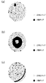
- FIG. 1 is a diagram illustrating an example of a distribution of defective chips.
- FIG. 2 is a diagram illustrating an example of a distribution pattern of defective chips.
- FIG. 3 is a diagram illustrating an example of the distribution of defective chips.
- FIG. 4 is a diagram illustrating an example of the distribution of defective chips.
- FIG. 5 is a diagram illustrating an example of the distribution of defective chips.
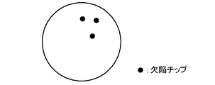
- FIG. 6 is a diagram illustrating the position of the defective chip in the two-dimensional space.
- FIG. 7 is a diagram showing the position of the defective chip in the three-dimensional space.
- FIG. 8 is a diagram showing the position of the defective chip in the two-dimensional space.
- FIG. 9 is a diagram showing the position of the defective chip in the three-dimensional space.
- FIG. 1 is a diagram illustrating an example of a distribution of defective chips.
- FIG. 2 is a diagram illustrating an example of a distribution pattern of defective chips.
- FIG. 3 is a diagram illustrating an example of the distribution of
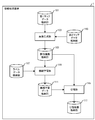
- FIG. 10 is a functional block diagram of the information processing apparatus.
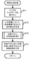
- FIG. 11 is a diagram showing a main processing flow.
- FIG. 12 is a diagram illustrating a processing flow of image generation processing.
- FIG. 13 is a diagram illustrating an example of the value of ⁇ .
- FIG. 14 is a diagram illustrating an example of the distribution of defective chips.
- FIG. 15 is a diagram illustrating a processing flow of the extension vector generation processing.
- FIG. 16 is a diagram illustrating an example of a bar code diagram.
- FIG. 17 is a diagram illustrating an example of barcode data.
- FIG. 18 is a diagram for explaining the relationship between the barcode data and the Betch series.
- FIG. 19 is a diagram illustrating an example of a persistent section.
- FIG. 20 is a diagram for explaining the feature image.
- FIG. 20 is a diagram for explaining the feature image.
- FIG. 21 is a diagram illustrating a processing flow of processing for classifying map data.
- FIG. 22 is a diagram illustrating an example of the distribution of defective chips.
- FIG. 23 is a diagram illustrating an example of the distribution of defective chips.
- FIG. 24 is a diagram illustrating an example of the distribution of defective chips.
- FIG. 25 is a diagram illustrating the feature amount extracted based on the Radon transform.
- FIG. 26 is a diagram illustrating feature amounts extracted by a method using persistent homology.
- FIG. 27 is a diagram illustrating an example of a feature image.
- FIG. 28 is a diagram illustrating an example of a feature image.
- FIG. 29 is a diagram illustrating an example of a feature image.
- FIG. 30 is a functional block diagram of a computer.
- FIG. 2 is a diagram showing an example of a defective chip distribution pattern.
- the distribution pattern in FIG. 2A is called “cluster”, and there are massive defective chips. In determining whether or not it is a cluster, the position from the center of the wafer, the size of the distribution, the density of the distribution, and the BIN are considered. On the other hand, the rotation of the wafer is basically not considered (that is, if one distribution pattern becomes the same as another distribution pattern due to the rotation of the wafer, both are considered to be the same distribution pattern).
- the distribution pattern in FIG. 2B is a distribution pattern called a “ring”, and annularly distributed defective chips exist in the center of the wafer.
- a ring the position from the center of the wafer, the shape of the distribution (for example, a circle or a semicircle), the size of the distribution, the density of the distribution, and the BIN are considered.
- the rotation of the wafer is not considered.
- the distribution pattern of FIG. 2C is a distribution pattern called “scratch”, and there are linearly distributed defective chips. In determining whether or not it is a scratch, the shape of the distribution (for example, a straight line or an arc), the number of lines, and the like are considered. On the other hand, the position from the center of the wafer, Wafer rotation and BIN are not considered.
- the cause of the defective chip may be identified by visually confirming the distribution of the defective chip on the newly manufactured wafer. is there.
- the relationship between the distribution shown in FIG. 3 and the distribution shown in FIG. 4A corresponds to the rotation of the wafer, and since the distance from the center of the wafer is the same, it is assumed that both distributions are the same. Is preferred.
- the relationship between the distribution shown in FIG. 3 and the distribution shown in FIG. 4 (b) corresponds to the parallel movement of the defective chip, and the distance from the center of the wafer is different. It may be preferable.
- the relationship between the distribution shown in FIG. 3 and the distribution shown in FIG. 4C corresponds to the rotation of the distribution itself and the direction from the center of the wafer is different, both distributions are considered to be different. May be preferred.
- FIG. 5 is a diagram illustrating an example of the distribution of defective chips.
- the relationship between the three distributions shown in FIGS. 5A to 5C corresponds to parallel movement.
- the parallel movement distance between the distribution in FIG. 5A and the distribution in FIG. 5B is shorter than the parallel movement distance between the distribution in FIG. 5A and the distribution in FIG.
- the point positional relationship is the same in the case of three-dimensional coordinates, even though the positional relationship of the points is different in the case of two-dimensional coordinates. It may become.
- the positional relationship of three defective chips shown in FIG. 8A is different from the positional relationship of three defective chips shown in FIG.
- the distance between the three sides of the triangle is 0.227, 0.227, and 0.4 as shown in FIGS. The distance relationship is exactly the same. That is, since the positional relationship between the three points is exactly the same, even if feature information extracted by persistent homology processing is used, proper classification cannot be performed.
- machine learning and classification are executed using feature information extracted by the following method.
- FIG. 10 is a functional block diagram of the information processing apparatus 1 according to the present embodiment.
- the information processing apparatus 1 includes a first map data storage unit 101, an image generation unit 103, a feature image storage unit 105, a label data storage unit 107, a machine learning unit 109, a machine learning data storage unit 111, a first 2 map data storage part 113, classification part 115, and classification result storage part 117 are included.
- the image generation unit 103, the machine learning unit 109, and the classification unit 115 are realized by executing a program loaded in the memory 2501 illustrated in FIG. 30 on a CPU (Central Processing Unit) 2503 illustrated in FIG.
- the first map data storage unit 101, the feature image storage unit 105, the label data storage unit 107, the machine learning data storage unit 111, the second map data storage unit 113, and the classification result storage unit 117 are shown in the memory 2501 or FIG.
- An HDD (Hard Disk Disk Drive) 2505 is provided.
- the image generation unit 103 executes processing based on the data stored in the first map data storage unit 101 and the data stored in the second map data storage unit 113 and stores the processing result in the feature image storage unit 105. To do.
- the machine learning unit 109 executes processing based on the data stored in the feature image storage unit 105 and the data stored in the label data storage unit 107 and stores the processing result in the machine learning data storage unit 111.
- the classification unit 115 executes processing based on the data stored in the feature image storage unit 105 and the data stored in the machine learning data storage unit 111 and stores the processing result in the classification result storage unit 117.
- step S1 the image generation unit 103 executes image generation processing.
- the image generation process will be described with reference to FIGS.
- the image generation unit 103 reads map data of defective chips on the wafer from the first map data storage unit 101 (FIG. 12: step S11). It is assumed that the label corresponding to the map data stored in the first map data storage unit 101 is known in advance.
- the map data includes information that can specify the two-dimensional coordinates of the defective chip (the origin is the center of the wafer).
- the image generation unit 103 generates a set of points represented by the extended coordinates from the read map data for each value of the contribution parameter ⁇ (step S13).
- the image generation unit 103 stores a set of points generated for each value of the contribution parameter ⁇ in the memory 2501.
- step S13 extended coordinates are generated for each defective chip.
- the extended coordinates are three-dimensional coordinates, and the x and y coordinates are specified from the map data.
- z may be set by another function. Specifically, it may be a monotonically increasing function reflecting the distance from the center of the wafer and a function having a constant first derivative. Alternatively, it may be a monotonically increasing function reflecting the distance from the wafer center and rotated about the z-axis.
- the contribution parameter ⁇ for example, a real number satisfying 0 ⁇ ⁇ ⁇ 1.
- the range of ⁇ may not be such a range.
- a plurality of values set at regular intervals are used.
- the magnitude of the change in the position of the point when the contribution parameter ⁇ is changed represents the distance from the center of the wafer. For example, in the portion close to the center of the wafer, even if ⁇ is changed, the change in the z coordinate is relatively small, and therefore the position change of the point when ⁇ is changed is relatively small. On the other hand, in the portion far from the center of the wafer, the change of the z coordinate when ⁇ is changed is relatively large, so that the position change of the point when ⁇ is changed is relatively large. That is, the distance from the center of the wafer can be estimated from the magnitude of the position change of the point when ⁇ is changed.
- the magnitude of the position change of the point when the contribution parameter ⁇ is changed represents the direction from the center of the wafer.
- the position change of the point when ⁇ is changed is relatively small.
- FIG. 14B when the density of defective chips on the center side of the wafer is smaller than the density of defective chips on the edge side of the wafer, the position change of the point when ⁇ is changed is relatively large. . Therefore, the direction from the center of the wafer can be estimated from the magnitude of the position change of the point when ⁇ is changed.
- the extended coordinates as in the present embodiment, it is possible to generate feature information reflecting the positional relationship of the defective chip, the distance from the center of the wafer, and the orientation from the center of the wafer. . Further, as is clear from the above description, “closeness” can also be estimated from the feature information.
- the image generation unit 103 executes an extended vector generation process using the set of points stored in the memory 2501 (step S15).
- the extended vector generation process will be described with reference to FIGS.
- the image generation unit 103 identifies one unprocessed value among the values of the contribution parameter ⁇ (FIG. 15: Step S21).
- the image generation unit 103 reads a set of points for the values specified in step S21 from the memory 2501 (step S23).
- the image generation unit 103 generates barcode data from a set of points for each hole dimension (hereinafter referred to as hole dimension) by persistent homology processing (step S25).
- “Homology” is a technique for expressing the characteristics of an object by the number of holes of m (m ⁇ 0) dimensions.
- the “hole” referred to here is an element of a homology group.
- a zero-dimensional hole is a connected component, a one-dimensional hole is a hole (tunnel), and a two-dimensional hole is a cavity.
- the number of holes in each dimension is called the Betch number.
- Persistent homology is a technique for characterizing the transition of an m-dimensional hole in an object (here, a set of points), and the characteristics regarding the arrangement of points can be examined by persistent homology.
- each point in the object is gradually inflated into a spherical shape, and the time when each hole occurs (represented by the radius of the sphere at the time of occurrence) and the time of disappearance (by the radius of the sphere at the time of disappearance) Specified).
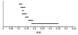
- a bar code diagram as shown in FIG. 16 can be generated by using the generation radius and the extinction radius of the hole.
- the horizontal axis represents the radius, and each line segment corresponds to one hole.
- the radius corresponding to the left end of the line segment is the generation radius of the hole, and the radius corresponding to the right end of the line segment is the disappearance radius of the hole.
- the line segment is called a persistent section. From such a bar code diagram, for example, it can be seen that there are two holes when the radius is 0.18.
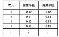
- FIG. 17 shows an example of data for generating a barcode diagram (hereinafter referred to as barcode data).
- barcode data a numerical value representing a hole dimension, a hole generation radius, and a hole disappearance radius are included.
- step S25 barcode data is generated for each hole dimension.
- the similarity between barcode data generated from a set of points and barcode data generated from another set of points is equivalent to the similarity between points. It is. Therefore, the relationship between the set of points and the barcode data is a one-to-one relationship.
- the generated barcode data is the same. Conversely, if the barcode data is the same, the set of points is the same. Further, when the set of points is similar, the barcode data is also similar, so the conditions necessary for machine learning are satisfied. When the set of points is different, the barcode data is also different.
- the image generation unit 103 deletes the data of the persistent section whose length is less than the predetermined length from the barcode data generated in step S25 (step S27).
- the length of the persistent section is calculated by (annihilation radius ⁇ generation radius).
- the predetermined length is, for example, the length of time (hereinafter referred to as a block) obtained by dividing the time from when a zero-dimensional hole is generated until it disappears into K.
- the length is not limited to one block, and a plurality of blocks may have a predetermined length.
- the origin of the short time from occurrence to disappearance is mostly caused by noise. If the data of the persistent section whose length is less than the predetermined length is deleted, the influence of noise can be mitigated, so that the classification performance can be improved. However, it is assumed that the object of deletion is persistent section data having a dimension of 1 or more.
- step S27 If there is noise, a one-dimensional or more hole may occur for a short time. If the process of step S27 is executed, the data generated in both cases will be substantially the same, so the influence of noise can be removed.
- the similarity relationship between the barcode data after deletion is not strictly equivalent to the similarity relationship between the original barcode data. If the deletion is not performed, the similarity relationship is equivalent.
- the image generation unit 103 integrates the barcode data, and generates an extension vector (the extension vector is a series of Betch numbers) from the integrated barcode data (step S29).
- the image generation unit 103 since barcode data is generated for each hole dimension, the image generation unit 103 generates a single piece of barcode data by integrating a plurality of hole dimension barcode data.
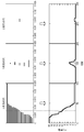
- the series of the number of vetches is data indicating the relationship between the radius (that is, time) of the sphere and the number of the vetches in the persistent homology. The relationship between the barcode data and the generated sequence of the number of vetches will be described with reference to FIG.
- the upper graph is a graph generated from the barcode data, and the horizontal axis represents the radius.
- the lower graph is a graph generated from a series of the number of vetches, the vertical axis represents the number of vetches, and the horizontal axis represents time.
- the number of holes represents the number of holes.
- the number of holes existing at the radius corresponding to the broken line is 10, so in the lower graph, the number of holes is broken.
- the corresponding number of vetches is also ten.
- the number of vetches is counted for each block. Since the lower graph is a pseudo time-series data graph, the value on the horizontal axis itself is not meaningful.
- the same series can be obtained from the same barcode data. That is, the same sequence is obtained if the original set of points is the same. However, there are very rare cases where the same sequence can be obtained from different barcodes.
- this barcode data is data relating to holes of one or more dimensions.
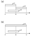
- the persistent section p1 starts at time t1 and ends at time t2, and the persistent section p2 starts at time t2 and ends at time t3.
- the persistent section p4 starts at time t1 and ends at time t3. It is assumed that the persistent section p3 in both cases is exactly the same.
- the similarity between a series of vetch numbers generated from one barcode data and a series of vetch numbers generated from another barcode data is the same as the above-mentioned rare case. It is equivalent to the similarity between code data. From the above, although the definition of the distance between the data changes, the similarity relationship between the series of Betch numbers generated from the barcode data is almost equivalent to the similarity relationship between the original set of points.
- step S31 determines whether there is an unprocessed value among the values of ⁇ . When there is an unprocessed value (step S31: Yes route), the process returns to step S21. If there is no unprocessed value (step S31: No route), the process returns to the caller.
- the distribution of defective chips represented by a set of points represented by extended coordinates can be reflected in the barcode data.
- classification according to the distribution of defective chips can be performed by machine learning.
- the barcode data generated by persistent homology processing is difficult to use as input for machine learning because the number of barcodes is not constant. Therefore, in the present embodiment, the barcode data is converted into a series of Betch numbers so that it can be used as an input for machine learning.
- the influence of noise can be removed.
- the image generation unit 103 generates a feature image by combining the plurality of extension vectors generated in step S15 in the order of the value of ⁇ (step S17), and the generated feature.
- the image is stored in the feature image storage unit 105. Processing then returns to the caller.
- FIG. 20 is a diagram illustrating an example of a feature image.
- a square figure represents a cell, and each cell stores the number of vetches that are elements of an expansion vector.
- One row corresponds to one extension vector. Therefore, in the example of FIG. 20, 11 extension vectors are combined, and the feature image corresponds to a matrix having 11 rows.
- the number of elements of the extension vector is 15, but the number is not limited.
- the machine learning unit 109 reads from the label data storage unit 107 a label corresponding to the feature image stored in the feature image storage unit 105.
- the label corresponding to the map data stored in the first map data storage unit 101 is known in advance, the label corresponding to the feature image stored in the feature image storage unit 105 can be specified.
- the label is, for example, information on the distribution pattern name of the defective chip. Then, the machine learning unit 109 associates the read label with the feature image stored in the feature image storage unit 105 (step S3).
- the machine learning unit 109 performs machine learning using the feature image stored in the feature image storage unit 105 and the label associated with the feature image (step S5). For example, machine learning using a neural network is executed.
- the machine learning unit 109 stores machine learning data (for example, an updated weight matrix) in the machine learning data storage unit 111. Then, the process ends.
- the image generation unit 103 executes an image generation process (FIG. 21: step S41).
- the image generation process is the same as that described with reference to FIGS.
- the map data stored in the second map data storage unit 113 is processed. It is assumed that the label corresponding to the map data stored in the second map data storage unit 113 is unknown. For example, newly generated map data for specifying a problem of an operating manufacturing apparatus is stored in the second map data storage unit 113.
- the classification unit 115 classifies the feature image generated in step S41 based on the machine learning data stored in the machine learning data storage unit 111 (step S43). For example, classification using a neural network is performed.
- the classification unit 115 stores the result of the classification executed in step S43 in the classification result storage unit 117 (step S45). For example, in association with the feature image generated in step S41, the label of the class to which the feature image belongs is stored in the classification result storage unit 117. Then, the process ends.
- the three wafers shown in FIGS. 22 to 24 are targeted.
- the wafer w1 in FIG. 22 and the wafer w2 in FIG. 23 should be classified into different classes because they have similar distribution shapes but different distribution positions.
- the wafer w1 in FIG. 22 and the wafer w3 in FIG. 24 should be classified into different classes because the cause of the defect is different although the distribution positions of the defective chips are approximately the same.
- FIG. 25 is a diagram showing feature amounts extracted based on Radon transformation.
- the left half of the graph shown in FIG. 25 is an average graph, and the right half of the graph shown in FIG. 25 is a variance graph.
- the horizontal axis represents the number of divisions, and the vertical axis represents the mean and variance values.
- the shape of the solid line is different from the shape of the dotted line, but the solid line and the broken line almost overlap each other. Therefore, if the classification is performed based on the feature amount shown in FIG. 25, the wafer w1 and the wafer w3 may be classified into the same class.
- FIG. 26 is a diagram showing feature amounts (that is, a series of Betch numbers) extracted by the method using persistent homology described with reference to FIGS.
- the left half of the graph shown in FIG. 26 is a graph of the number of vetches for the zeroth order
- the right half of the graph shown in FIG. 26 is a graph of the number of vetches for the first order.
- the horizontal axis represents the radius
- the vertical axis represents the number of vetches.
- the shape of the solid line is different from the shape of the broken line, but the solid line and the dotted line almost overlap each other. Therefore, when classification is performed based on the feature amount shown in FIG. 26, the wafer w1 and the wafer w2 may be classified into the same class.
- FIG. 27 to 29 are diagrams showing feature images generated by the method of the present embodiment.
- FIG. 27 is a diagram showing a feature image of the wafer w1
- FIG. 28 is a diagram showing a feature image of the wafer w2
- FIG. 29 is a diagram showing a feature image of the wafer w3. Comparing the feature image of the wafer w1 and the feature image of the wafer w2, there is a difference in the density of the white area. Further, when the feature image of the wafer w1 and the feature image of the wafer w3 are compared, there is a difference in the shape of the white area. Therefore, if classification is performed based on the feature image generated by the method of the present embodiment, there is a possibility that the wafer w1 can be classified into a different class from the wafer w2 and the wafer w3.
- the present invention is not limited to this.
- the functional block configuration of the information processing apparatus 1 described above may not match the actual program module configuration.
- the data configuration described above is an example, and it does not have to be the above configuration. Further, in the processing flow, the processing order can be changed if the processing result does not change. Further, it may be executed in parallel.
- each distribution pattern there are random defects that are different from the systematic defects that occur due to causes unique to the manufacturing process of the IC chip.
- the defects targeted in this embodiment are systematic defects.
- the information processing apparatus 1 described above is a computer apparatus, and as shown in FIG. 30, a display controller 2507 connected to a memory 2501, a CPU 2503, an HDD 2505, a display device 2509, and a removable disk 2511.
- a drive device 2513, an input device 2515, and a communication control unit 2517 for connecting to a network are connected by a bus 2519.
- An operating system (OS: Operating System) and an application program for performing the processing in this embodiment are stored in the HDD 2505, and are read from the HDD 2505 to the memory 2501 when executed by the CPU 2503.
- the CPU 2503 controls the display control unit 2507, the communication control unit 2517, and the drive device 2513 according to the processing content of the application program, and performs a predetermined operation.
- data in the middle of processing is mainly stored in the memory 2501, but may be stored in the HDD 2505.
- an application program for performing the above-described processing is stored in a computer-readable removable disk 2511 and distributed, and installed in the HDD 2505 from the drive device 2513.
- the HDD 2505 may be installed via a network such as the Internet and the communication control unit 2517.
- Such a computer apparatus realizes various functions as described above by organically cooperating hardware such as the CPU 2503 and the memory 2501 described above and programs such as the OS and application programs. .
- a Betch number series (for example, an extension vector) is generated by persistent homology processing for a plurality of extended coordinates, and (C) for each of a plurality of wafers, from a plurality of Betch number series generated for a plurality of contribution parameter values,
- a defect pattern image (for example, a feature image) is generated, and (D) a plurality of defect pattern images generated for a plurality of wafers and a plurality of windows are generated. It includes a process of generating a machine learning data that associates identification information associated with the wafer.
- the wafer defect position information is converted into a defect pattern image suitable for classification.
- the defect pattern image may be generated by combining a plurality of Betch number sequences in the order of the contribution parameter values.
- a defect pattern image reflecting the distance from the wafer center and the orientation from the wafer center can be generated.
- (b1) by connecting the time series data of the Betch number of each dimension generated by the persistent homology processing with respect to the generated plurality of extended coordinates, It may be generated.
- the value representing the position on the wafer includes the value of the first axis and the value of the second axis orthogonal to the first axis, and the value calculated from the distance from the center and the value of the contribution parameter is It may be a value obtained by multiplying a value representing a distance from the contribution parameter value and a value on a third axis orthogonal to the first axis and the second axis.
- the discrimination information may be a label.
- the data generation apparatus uses (E) the information on the defect position of the wafer for each of the plurality of wafers, for each defect on the wafer, In addition, an extended coordinate including a value calculated from the distance from the center of the wafer and the contribution parameter is generated, and for each of the plurality of wafers, a Betch number series is obtained by persistent homology processing for the generated multiple extended coordinates.
- a first generation unit that generates a defect pattern image from a plurality of Betch number sequences generated for a plurality of values of contribution parameters for each of a plurality of wafers (the image generation unit 103 in the embodiment is a first generation unit).
- Second generating unit for generating a machine learning data that associates broadcast (machine learning unit 109 in the embodiment, a is an example of a second generating unit) and a.
- a program for causing the processor to perform the processing according to the above method can be created.
- the program is, for example, a computer-readable storage medium such as a flexible disk, CD-ROM, magneto-optical disk, semiconductor memory, or hard disk. It is stored in a storage device.
- the intermediate processing result is temporarily stored in a storage device such as a main memory.
- Generate extended coordinates including For each of the plurality of wafers, generate a Betch number series by persistent homology processing for the generated plurality of extended coordinates, For each of the plurality of wafers, generate a defect pattern image from a plurality of Betch number sequences generated for a plurality of values of the contribution parameter, Generating machine learning data associating a plurality of defect pattern images generated for the plurality of wafers with discrimination information associated with the plurality of wafers; Data generation program that executes processing.
- the value representing the position on the wafer includes a value of a first axis and a value of a second axis orthogonal to the first axis,
- the value calculated from the distance from the center and the value of the contribution parameter is a value obtained by multiplying the value representing the distance from the center by the value of the contribution parameter, and the first axis and the second axis.
- a value on the third axis orthogonal to The data generation program according to any one of supplementary notes 1 to 3.
- the discrimination information is a label.
- the data generation program according to any one of appendices 1 to 4.
- a first generation unit that generates a defect pattern image from a plurality of Betch number sequences generated;
- a second generation unit that generates machine learning data in which a plurality of defect pattern images generated for the plurality of wafers are associated with discrimination information associated with the plurality of wafers;
- a data generation apparatus that generates a defect pattern image from a plurality of Betch number sequences generated.
Landscapes
- Engineering & Computer Science (AREA)
- Theoretical Computer Science (AREA)
- Physics & Mathematics (AREA)
- General Physics & Mathematics (AREA)
- Software Systems (AREA)
- Computer Vision & Pattern Recognition (AREA)
- Artificial Intelligence (AREA)
- Evolutionary Computation (AREA)
- Computing Systems (AREA)
- General Health & Medical Sciences (AREA)
- Health & Medical Sciences (AREA)
- Mathematical Physics (AREA)
- Data Mining & Analysis (AREA)
- General Engineering & Computer Science (AREA)
- Life Sciences & Earth Sciences (AREA)
- Medical Informatics (AREA)
- Quality & Reliability (AREA)
- Biomedical Technology (AREA)
- Computational Linguistics (AREA)
- Biophysics (AREA)
- Molecular Biology (AREA)
- Biochemistry (AREA)
- Chemical & Material Sciences (AREA)
- Analytical Chemistry (AREA)
- Immunology (AREA)
- Pathology (AREA)
- Multimedia (AREA)
- Databases & Information Systems (AREA)
- Testing Or Measuring Of Semiconductors Or The Like (AREA)
- Investigating Materials By The Use Of Optical Means Adapted For Particular Applications (AREA)
Abstract
【課題】ウエハ上の欠陥チップの位置情報を、分類に適した特徴情報に変換する。 【解決手段】本データ生成方法は、複数のウエハそれぞれについて、当該ウエハの欠陥位置の情報を用いて、当該ウエハ上の欠陥ごとに、当該ウエハ上の位置、および、当該ウエハの中心からの距離と寄与パラメータとから算出される値を含む拡張座標を生成し、複数のウエハそれぞれについて、生成された複数の拡張座標に対するパーシステントホモロジ処理によりベッチ数系列を生成し、複数のウエハそれぞれについて、寄与パラメータの複数の値に対し生成した複数のベッチ数系列から、欠陥パターン画像を生成し、複数のウエハについて生成された複数の欠陥パターン画像と、複数のウエハに対応付けられた判別情報とを対応付けた機械学習データを生成する処理を含む。
Description
本発明は、ウエハにおける欠陥の情報の処理技術に関する。
ウエハ上に発生する欠陥の分布の形状が複数のウエハ間で類似している場合、それらのウエハの加工における同一の工程が欠陥の原因であることがある。そのため、欠陥を有するICチップ(以下、欠陥チップと呼ぶ)のウエハ上の位置の情報に基づいて、問題が有る工程を特定することが行われている。
例えば、或る文献は、欠陥チップのマップデータに対するラドン変換により生成されたデータから特徴量を抽出し、抽出した特徴量に基づいて欠陥の原因を特定する技術を開示する。
Ming-Ju Wu、Jyh-Shing R. Jang、Jui-Long Chen、"Wafer Map Failure Pattern Recognition and Similarity Ranking for Large-Scale Data Sets"、IEEE Transactions on Semiconductor Manufacturing、平成27年2月、第28巻、第1号、pp.1-12
しかし、上記文献の技術を利用することが適切ではないケースが存在する。例えば図1(a)に示したウエハと図1(b)に示したウエハとを比較すると、欠陥チップのウエハ上での分布位置はおおよそ同じであるものの、分布の形状は異なっている。このようなケースにおいては、図1(a)に示した欠陥チップの原因と図1(b)に示した欠陥チップの原因とが異なる可能性があるが、上記文献の技術を利用した場合、原因は同じであると判定されることがある。
本発明の目的は、1つの側面では、ウエハ上の欠陥チップの位置情報を、分類に適した特徴情報に変換することである。
一態様に係るデータ生成方法は、複数のウエハそれぞれについて、当該ウエハの欠陥位置の情報を用いて、当該ウエハ上の欠陥ごとに、当該ウエハ上の位置、および、当該ウエハの中心からの距離と寄与パラメータとから算出される値を含む拡張座標を生成し、複数のウエハそれぞれについて、生成された複数の拡張座標に対するパーシステントホモロジ処理によりベッチ数系列を生成し、複数のウエハそれぞれについて、寄与パラメータの複数の値に対し生成した複数のベッチ数系列から、欠陥パターン画像を生成し、複数のウエハについて生成された複数の欠陥パターン画像と、複数のウエハに対応付けられた判別情報とを対応付けた機械学習データを生成する処理を含む。
1つの側面では、ウエハ上の欠陥チップの位置情報を、分類に適した特徴情報に変換できる。
図2は、欠陥チップの分布パターンの一例を示す図である。
図2(a)の分布パターンは「クラスタ」と呼ばれ、塊状の欠陥チップが存在する。クラスタであるか否かの判定においては、ウエハの中心からの位置、分布の大きさ、分布の濃さおよびBINが考慮される。一方で、ウエハの回転は基本的には考慮されない(すなわち、或る分布パターンがウエハの回転により別の分布パターンと同じになる場合、両者は同じ分布パターンであると見做される)。
図2(b)の分布パターンは「リング」と呼ばれる分布パターンであり、環状に分布した欠陥チップがウエハの中央に存在する。リングであるか否かの判定においては、ウエハの中心からの位置、分布の形状(例えば、円または半円)、分布の大きさ、分布の濃さ及びBINが考慮される。一方で、ウエハの回転は考慮されない。
図2(c)の分布パターンは「スクラッチ」と呼ばれる分布パターンであり、線状に分布した欠陥チップが存在する。スクラッチであるか否かの判定においては、分布の形状(例えば、直線または円弧)及び線の数等が考慮される。一方、ウエハの中心からの位置、
ウエハの回転及びBINは考慮されない。
ウエハの回転及びBINは考慮されない。
欠陥チップが発生した原因毎に分布パターンを予め特定しておけば、新たに製造されたウエハ上の欠陥チップの分布を目視で確認することで、欠陥チップが発生した原因を特定できる可能性がある。但し、欠陥チップが生じる原因は様々であり、そのため分布のバリエーションは非常に多いため、分類は容易ではない。
そこで、以下では、欠陥チップの位置情報そのものではなく、欠陥チップの位置情報から抽出した特徴情報を基にして分類を行うことについて検討する。
図3乃至図5を用いて、特徴情報の要件を検討する。図3に示した分布と図4(a)に示した分布との関係はウエハの回転に該当し、ウエハの中心からの距離が同じであるので、両分布は同じであると見做すことが好ましい。一方で、図3に示した分布と図4(b)に示した分布との関係は欠陥チップの平行移動に該当し、ウエハの中心からの距離が異なるので、両分布は異なると見做すことが好ましい場合が有る。また、図3に示した分布と図4(c)に示した分布との関係は分布自体の回転に該当し、ウエハの中心からの向きが異なるので、両分布は異なるものと見做すことが好ましい場合が有る。
また、分布パターン同士の「近さ」(すなわち距離)を判定できることが好ましい。図5は、欠陥チップの分布の一例を示す図である。図5(a)乃至図5(c)に示した3つの分布の関係は平行移動に該当する。図5(a)の分布と図5(b)の分布との間の平行移動距離は、図5(a)の分布と図5(c)の分布との間の平行移動距離より短い。このようなケースの場合、図5(a)の分布と図5(b)の分布は同じであると見做すことが好ましい場合があるが、図5(a)の分布と図5(c)の分布は異なると見做すことが好ましい場合がある。
以上を踏まえると、特徴情報に以下が反映されることが好ましい。
(1)欠陥チップの位置関係(すなわち分布の形状)
(2)ウエハの中心からの距離
(3)ウエハの中心からの向き
(4)上記(1)乃至(3)の情報の「近さ」
(1)欠陥チップの位置関係(すなわち分布の形状)
(2)ウエハの中心からの距離
(3)ウエハの中心からの向き
(4)上記(1)乃至(3)の情報の「近さ」
ここで、点の配置情報を類型化することが可能な手法であるパーシステントホモロジ(Persistent Homology)を用いて特徴情報を抽出することについて検討する。但し、パーシステントホモロジ処理を実行すると、ウエハの回転を無視することができるものの、中心からの距離および中心からの向きは特徴情報に反映されない。
そこで、ウエハ上の欠陥チップの位置を表す二次元座標(x,y)に対して、中心からの距離に応じた高さの軸(ここではz軸とする)の値を加えることで、二次元座標(x,y)を三次元座標(x,y,z)に変換することを考える。zは、例えば、z=x2+y2として設定される。
このようなz軸の値を設定しない場合、図6(a)に示した3つの欠陥チップの2次元座標に対して実行したパーシステントホモロジ処理の結果と、図6(b)に示した3つの欠陥チップの2次元座標に対して実行したパーシステントホモロジ処理の結果とは同じになる。この理由は、両者を平行移動により重ねることが可能であり、3点の位置関係は全く同じであるからである。
しかし、上記のようにz軸の値が設定された三次元座標を生成すると、図7(a)及び図7(b)に示すように、3点の位置関係が同一ではなくなる。従って、中心からの距離が反映された三次元座標の導入により、平行移動によって両者を重ねることができないようにすることができる。
但し、上記のような方法でz軸の値を設定すると、二次元座標の場合には点の位置関係が異なっていたにもかかわらず、三次元座標の場合には点の位置関係が同一になってしまうことがある。例えば、図8(a)に示した3つの欠陥チップの位置関係と、図8(b)に示した3つの欠陥チップの位置関係とは異なる。しかしながら、z軸の値を設定すると、図9(a)及び図9(b)に示すように、三角形の三辺の距離が0.227、0.227、0.4であり、点の間の距離関係が全く同じになる。つまり、3点の位置関係が全く同じになるので、パーシステントホモロジ処理によって抽出される特徴情報を使用したとしても、適切な分類をすることができない。
そこで本実施の形態においては、以下のような方法によって抽出された特徴情報によって機械学習及び分類を実行する。
図10は、本実施の形態の情報処理装置1の機能ブロック図である。情報処理装置1は、第1マップデータ格納部101と、画像生成部103と、特徴画像格納部105と、ラベルデータ格納部107と、機械学習部109と、機械学習データ格納部111と、第2マップデータ格納部113と、分類部115と、分類結果格納部117とを含む。
画像生成部103、機械学習部109および分類部115は、図30に示したメモリ2501にロードされたプログラムが図30に示したCPU(Central Processing Unit)2503に実行されることで実現される。第1マップデータ格納部101、特徴画像格納部105、ラベルデータ格納部107、機械学習データ格納部111、第2マップデータ格納部113および分類結果格納部117は、メモリ2501又は図30に示したHDD(Hard Disk Drive)2505に設けられる。
画像生成部103は、第1マップデータ格納部101に格納されているデータ及び第2マップデータ格納部113に格納されているデータに基づき処理を実行し、処理結果を特徴画像格納部105に格納する。機械学習部109は、特徴画像格納部105に格納されているデータ及びラベルデータ格納部107に格納されているデータに基づき処理を実行し、処理結果を機械学習データ格納部111に格納する。分類部115は、特徴画像格納部105に格納されているデータ及び機械学習データ格納部111に格納されているデータに基づき処理を実行し、処理結果を分類結果格納部117に格納する。
次に、図11乃至図29を用いて、情報処理装置1が実行する処理について説明する。
まず、画像生成部103は、画像生成処理を実行する(図11:ステップS1)。画像生成処理については、図12乃至図20を用いて説明する。
画像生成部103は、ウエハ上の欠陥チップのマップデータを第1マップデータ格納部101から読み出す(図12:ステップS11)。なお、第1マップデータ格納部101に格納されるマップデータに対応するラベルは予め判明しているものとする。マップデータは、欠陥チップの二次元座標(原点はウエハの中心)を特定可能な情報を含む。
画像生成部103は、寄与パラメータαの各値について、読み出したマップデータから拡張座標で表された点の集合を生成する(ステップS13)。画像生成部103は、寄与パラメータαの各値について生成した点の集合を、メモリ2501に格納する。
ステップS13においては、各欠陥チップについて拡張座標が生成される。拡張座標は三次元座標であり、x座標およびy座標はマップデータから特定される。z座標は、例えば、z=α*(x2+y2)により設定される。但し、別の関数によりzを設定してもよい。具体的には、ウエハの中心からの距離が反映された単調増加の関数であって且つ一階微分が一定である関数であってもよい。または、ウエハの中心からの距離が反映された単調増加の関数であってz軸の周りに回転された関数であってもよい。
寄与パラメータα、例えば、0≦α≦1を満たす実数である。但し、αの範囲はこのような範囲でなくてもよい。本実施の形態においては、例えば図13に示すように、一定の間隔で設定された複数の値が使用される。
寄与パラメータαを変化させた時の点の位置変化の大きさは、ウエハの中心からの距離を表す。例えば、ウエハの中心に近い部分においては、αを変化させてもz座標の変化が比較的小さいため、αを変化させた時の点の位置変化が比較的小さい。逆に、ウエハの中心から遠い部分においては、αを変化させた時のz座標の変化が比較的大きいため、αを変化させた時の点の位置変化が比較的大きい。つまり、αを変化させた時の点の位置変化の大きさから、ウエハの中心からの距離を推定することができる。
また、寄与パラメータαを変化させた時の点の位置変化の大きさは、ウエハの中心からの向きを表す。例えば図14(a)に示すように、ウエハの中心側の欠陥チップの密度がウエハの端側の欠陥チップの密度より大きい場合、αを変化させた時の点の位置変化が比較的小さい。一方、図14(b)に示すように、ウエハの中心側の欠陥チップの密度がウエハの端側の欠陥チップの密度より小さい場合、αを変化させた時の点の位置変化が比較的大きい。従って、αを変化させた時の点の位置変化の大きさから、ウエハの中心からの向きを推定することができる。
よって、本実施の形態のような拡張座標を導入することで、欠陥チップの位置関係、ウエハの中心からの距離およびウエハの中心からの向きを反映した特徴情報を生成することができるようになる。また、上記の説明から明らかなように、特徴情報により「近さ」をも推定することができる。
そして、画像生成部103は、メモリ2501に格納された点の集合を用いて、拡張ベクトル生成処理を実行する(ステップS15)。拡張ベクトル生成処理については、図15乃至図20を用いて説明する。
まず、画像生成部103は、寄与パラメータαの値のうち未処理の値を1つ特定する(図15:ステップS21)。
画像生成部103は、ステップS21において特定した値についての点の集合を、メモリ2501から読み出す(ステップS23)。
画像生成部103は、パーシステントホモロジ処理によって、点の集合からバーコードデータを穴の次元(以下、穴次元と呼ぶ)毎に生成する(ステップS25)。
「ホモロジ」とは、対象の特徴をm(m≧0)次元の穴の数によって表現する手法である。ここで言う「穴」とはホモロジ群の元のことであり、0次元の穴は連結成分であり、1次元の穴は穴(トンネル)であり、2次元の穴は空洞である。各次元の穴の数はベッチ数と呼ばれる。
「パーシステントホモロジ」とは、対象(ここでは、点の集合)におけるm次元の穴の遷移を特徴付けるための手法であり、パーシステントホモロジによって点の配置に関する特徴を調べることができる。この手法においては、対象における各点が球状に徐々に膨らまされ、その過程において各穴が発生した時刻(発生時の球の半径で表される)と消滅した時刻(消滅時の球の半径で表される)とが特定される。
穴の発生半径と消滅半径とを使用することで、例えば図16に示すようなバーコード図を生成することができる。図16において、横軸は半径を表し、各線分は1つの穴に対応する。線分の左端に対応する半径は穴の発生半径であり、線分の右端に対応する半径は穴の消滅半径である。線分はパーシステント区間と呼ばれる。このようなバーコード図から、例えば半径が0.18である時には2つの穴が存在するということがわかる。
図17に、バーコード図を生成するためのデータ(以下、バーコードデータと呼ぶ)の一例を示す。図17の例では、穴次元を表す数値と、穴の発生半径と、穴の消滅半径とが含まれる。ステップS25において、バーコードデータは穴次元毎に生成される。
以上のような処理を実行すれば、或る点の集合から生成されるバーコードデータと他の点の集合から生成されるバーコードデータとの類似関係は、点の集合間の類似関係と等価である。よって、点の集合とバーコードデータとの関係は1対1の関係である。
すなわち、点の集合が同じであれば、生成されるバーコードデータは同じである。逆に、バーコードデータが同じであれば、点の集合も同じである。また、点の集合が類似している場合にはバーコードデータも類似するため、機械学習に必要な条件が満たされる。点の集合が異なる場合には、バーコードデータも異なる。
なお、パーシステントホモロジの詳細については、例えば「平岡裕章、『タンパク質構造とトポロジー パーシステントホモロジー群入門』、共立出版」を参照されたい。
図15の説明に戻り、画像生成部103は、長さが所定長未満であるパーシステント区間のデータを、ステップS25において生成されたバーコードデータから削除する(ステップS27)。なお、パーシステント区間の長さは、(消滅半径-発生半径)によって算出される。所定長は、例えば、0次元の穴が発生してから消滅するまでの時間をK等分した時間(以下、ブロックと呼ぶ)の長さである。但し、1ブロックの長さに限られるわけではなく、複数ブロックの長さを所定長としてもよい。
発生から消滅までの時間が短い元は、ノイズによって発生するものがほとんどである。長さが所定長未満であるパーシステント区間のデータを削除すれば、ノイズの影響を緩和することができるので、分類性能を向上させることができるようになる。但し、削除の対象は次元が1以上であるパーシステント区間のデータであるとする。
ノイズが発生した場合においては、僅かな時間だけ1次元以上の穴が発生することがある。ステップS27の処理を実行すれば、両ケースにおいて生成されるデータはほぼ同じになるので、ノイズの影響を取り除くことができるようになる。
なお、長さが所定長未満であるパーシステント区間のデータが削除されるので、削除後のバーコードデータ間の類似関係は、元のバーコードデータ間の類似関係と厳密には等価ではない。削除が行われない場合には、類似関係は等価である。
図15の説明に戻り、画像生成部103は、バーコードデータを統合し、統合されたバーコードデータから拡張ベクトル(拡張ベクトルはベッチ数の系列である)を生成する(ステップS29)。
上で述べたように、バーコードデータは穴次元毎に生成されるので、画像生成部103は、複数の穴次元のバーコードデータを統合することで1塊のバーコードデータを生成する。ベッチ数の系列は、パーシステントホモロジにおける球の半径(すなわち時間)とベッチ数との関係を示すデータである。図18を用いて、バーコードデータと生成されるベッチ数の系列との関係について説明する。上段のグラフはバーコードデータから生成されるグラフであり、横軸が半径を表す。下段のグラフはベッチ数の系列から生成されるグラフであり、縦軸はベッチ数を表し、横軸は時間を表す。上で述べたように、ベッチ数は穴の数を表しており、例えば上段のグラフにおいて破線に対応する半径の時には存在している穴の数が10であるので、下段のグラフにおいては破線に対応するベッチ数も10である。ベッチ数は、ブロック毎に計数される。なお、下段のグラフは疑似的な時系列データのグラフであるので、横軸の値自体が意味を持つわけではない。
基本的には、同じバーコードデータからは同じ系列が得られる。すなわち、元の点の集合が同じであれば同じ系列が得られる。但し、異なるバーコードから同じ系列が得られるケースが極めて稀に発生する。
例えば図19に示すようなバーコードデータを考える。このバーコードデータは1以上の次元の穴に関するデータであるとする。図19(a)のケースにおいては、パーシステント区間p1が時刻t1で開始し且つ時刻t2で終了し、パーシステント区間p2が時刻t2で開始し且つ時刻t3で終了する。一方、図19(b)のケースにおいては、パーシステント区間p4が時刻t1で開始し且つ時刻t3で終了する。両ケースにおけるパーシステント区間p3は全く同じであるとする。
このような場合、両ケースにおけるバーコードデータからは全く同じ系列が得られるので、両ケースを区別することができない。しかし、このような現象が発生する可能性は極めて低い。また、両ケースの点の集合は元々似ており、機械学習による分類に与える影響が極めて小さいので、上記のような現象が発生しても問題は無い。
従って、或るバーコードデータから生成されるベッチ数の系列と、別のバーコードデータから生成されるベッチ数の系列との類似関係は、上で述べた稀なケースが発生しなければ、バーコードデータ間の類似関係と等価である。以上から、データ間の距離の定義は変わるものの、バーコードデータから生成されるベッチ数の系列間の類似関係は、元の点の集合間の類似関係とほぼ等価である。
図15の説明に戻り、画像生成部103は、αの値のうち未処理の値が有るか判定する(ステップS31)。未処理の値が有る場合(ステップS31:Yesルート)、ステップS21の処理に戻る。未処理の値が無い場合(ステップS31:Noルート)、処理は呼び出し元に戻る。
以上のように、パーシステントホモロジ処理を実行すれば、拡張座標で表された点の集合が表す、欠陥チップの分布を、バーコードデータに反映することができる。これにより、欠陥チップの分布に応じた分類を機械学習によって行うことができるようになる。
パーシステントホモロジ処理によって生成されたバーコードデータは、バーコードの本数が一定ではないため、そのままでは機械学習の入力とすることが難しい。そこで本実施の形態においては、バーコードデータをベッチ数の系列に変換することで、機械学習の入力とすることを可能にしている。
また、上で述べたように、本実施の形態によればノイズの影響を取り除くことができる。
図12の説明に戻り、画像生成部103は、ステップS15において生成された複数の拡張ベクトルを、αの値の大きさの順に結合することで特徴画像を生成し(ステップS17)、生成した特徴画像を特徴画像格納部105に格納する。そして処理は呼び出し元に戻る。
図20は、特徴画像の一例を示す図である。正方形の図形はセルを表し、各セルには拡張ベクトルの要素であるベッチ数が格納される。1つの行が1つの拡張ベクトルに対応する。従って、図20の例においては、11個の拡張ベクトルが結合されており、特徴画像は11の行を有する行列に相当する。図20においては拡張ベクトルの要素の数が15であるが、数に限定は無い。
図11の説明に戻り、機械学習部109は、特徴画像格納部105に格納された特徴画像に対応するラベルをラベルデータ格納部107から読み出す。なお、第1マップデータ格納部101に格納されるマップデータに対応するラベルは予め判明しているため、特徴画像格納部105に格納された特徴画像に対応するラベルを特定することができる。ラベルは、例えば、欠陥チップの分布パターン名の情報である。そして、機械学習部109は、特徴画像格納部105に格納された特徴画像に対して、読み出したラベルを対応付ける(ステップS3)。
機械学習部109は、特徴画像格納部105に格納された特徴画像と当該特徴画像に対応付けられたラベルとを用いて機械学習を実行する(ステップS5)。例えば、ニューラルネットワークを用いた機械学習が実行される。機械学習部109は、機械学習データ(例えば、更新後の重み行列等)を機械学習データ格納部111に格納する。そして処理は終了する。
以上のように、ウエハ上の欠陥の分布の特徴が適切に反映された特徴画像に基づき機械学習を実行すれば、後に実行する分類の精度を向上させることができるようになる。
次に、図21を用いて、図11乃至図20を用いて説明した処理の結果を利用してマップデータを分類する処理について説明する。
まず、画像生成部103は、画像生成処理を実行する(図21:ステップS41)。画像生成処理については、図12乃至図20を用いて説明したとおりであるので、説明を省略する。但し、ステップS41における画像生成処理においては、第2マップデータ格納部113に格納されているマップデータが処理される。第2マップデータ格納部113に格納されるマップデータに対応するラベルは不明であるものとする。例えば、稼働中の製造装置の問題を特定するため新規で生成されたマップデータが第2マップデータ格納部113に格納される。
分類部115は、ステップS41において生成された特徴画像を、機械学習データ格納部111に格納された機械学習データに基づき分類する(ステップS43)。例えば、ニューラルネットワークを用いた分類が行われる。
分類部115は、ステップS43において実行した分類の結果を分類結果格納部117に格納する(ステップS45)。例えば、ステップS41において生成された特徴画像に対応付けて、当該特徴画像が属するクラスのラベルが分類結果格納部117に格納される。そして処理は終了する。
以上のような処理を実行すれば、ICチップの製造における工程のうち問題が有る工程を特定することができるようになる。
以下では、本実施の形態の方法の効果を他の方法との比較をもとに説明する。
ここでは、図22乃至図24に示した3つのウエハを対象とする。前提として、図22のウエハw1と図23のウエハw2とは、分布の形状は類似しているものの分布位置が異なるため異なるクラスに分類されるべきであるとする。図22のウエハw1と図24のウエハw3とは、欠陥チップの分布位置はおおよそ同じであるものの欠陥の原因が異なるため異なるクラスに分類されるべきであるとする。
図25は、ラドン変換に基づき抽出された特徴量を示す図である。図25に示したグラフの左半分は平均についてのグラフであり、図25に示したグラフの右半分は分散についてのグラフである。横軸は分割の数を表し、縦軸は平均及び分散の値を表す。図25に示したグラフにおいて、実線の形状と点線の形状とは異なるが、実線と破線とがほぼ重なっている。従って、図25に示した特徴量に基づき分類を実行すると、ウエハw1とウエハw3とが同じクラスに分類される可能性がある。
図26は、図6乃至図9を用いて説明した、パーシステントホモロジを用いる方法で抽出された特徴量(すなわちベッチ数の系列)を示す図である。図26に示したグラフの左半分は0次についてのベッチ数のグラフであり、図26に示したグラフの右半分は1次についてのベッチ数のグラフである。横軸は半径を表し、縦軸はベッチ数を表す。図26に示したグラフにおいて、実線の形状と破線の形状とは異なるが、実線と点線とがほぼ重なっている。従って、図26に示した特徴量に基づき分類を実行すると、ウエハw1とウエハw2とが同じクラスに分類される可能性がある。
図27乃至図29は、本実施の形態の方法により生成された特徴画像を示す図である。図27はウエハw1の特徴画像を示す図であり、図28はウエハw2の特徴画像を示す図であり、図29はウエハw3の特徴画像を示す図である。ウエハw1の特徴画像とウエハw2の特徴画像とを比較すると、白い領域の濃さに相違がある。また、ウエハw1の特徴画像とウエハw3の特徴画像とを比較すると、白い領域の形状に相違がある。従って、本実施の形態の方法により生成された特徴画像に基づき分類を実行すれば、ウエハw1をウエハw2及びウエハw3とは別のクラスに分類できる可能性がある。
以上本発明の一実施の形態を説明したが、本発明はこれに限定されるものではない。例えば、上で説明した情報処理装置1の機能ブロック構成は実際のプログラムモジュール構成に一致しない場合もある。
また、上で説明したデータ構成は一例であって、上記のような構成でなければならないわけではない。さらに、処理フローにおいても、処理結果が変わらなければ処理の順番を入れ替えることも可能である。さらに、並列に実行させるようにしても良い。
なお、各分布パターンには、ICチップの製造工程固有の原因で発生するシステマチック欠陥とは異なるランダム欠陥が存在するが、本実施の形態において対象とされる欠陥はシステマチック欠陥である。
なお、上で述べた情報処理装置1は、コンピュータ装置であって、図30に示すように、メモリ2501とCPU2503とHDD2505と表示装置2509に接続される表示制御部2507とリムーバブル・ディスク2511用のドライブ装置2513と入力装置2515とネットワークに接続するための通信制御部2517とがバス2519で接続されている。オペレーティング・システム(OS:Operating System)及び本実施例における処理を実施するためのアプリケーション・プログラムは、HDD2505に格納されており、CPU2503により実行される際にはHDD2505からメモリ2501に読み出される。CPU2503は、アプリケーション・プログラムの処理内容に応じて表示制御部2507、通信制御部2517、ドライブ装置2513を制御して、所定の動作を行わせる。また、処理途中のデータについては、主としてメモリ2501に格納されるが、HDD2505に格納されるようにしてもよい。本発明の実施例では、上で述べた処理を実施するためのアプリケーション・プログラムはコンピュータ読み取り可能なリムーバブル・ディスク2511に格納されて頒布され、ドライブ装置2513からHDD2505にインストールされる。インターネットなどのネットワーク及び通信制御部2517を経由して、HDD2505にインストールされる場合もある。このようなコンピュータ装置は、上で述べたCPU2503、メモリ2501などのハードウエアとOS及びアプリケーション・プログラムなどのプログラムとが有機的に協働することにより、上で述べたような各種機能を実現する。
以上述べた本発明の実施の形態をまとめると、以下のようになる。
本実施の形態の第1の態様に係るデータ生成方法は、(A)複数のウエハそれぞれについて、当該ウエハの欠陥位置の情報(例えばマップデータ)を用いて、当該ウエハ上の欠陥ごとに、当該ウエハ上の位置(例えばx座標およびy座標)、および、当該ウエハの中心からの距離と寄与パラメータとから算出される値を含む拡張座標を生成し、(B)複数のウエハそれぞれについて、生成された複数の拡張座標に対するパーシステントホモロジ処理によりベッチ数系列(例えば拡張ベクトル)を生成し、(C)複数のウエハそれぞれについて、寄与パラメータの複数の値に対し生成した複数のベッチ数系列から、欠陥パターン画像(例えば特徴画像)を生成し、(D)複数のウエハについて生成された複数の欠陥パターン画像と、複数のウエハに対応付けられた判別情報とを対応付けた機械学習データを生成する処理を含む。
ウエハの欠陥位置の情報が、分類に適した欠陥パターン画像に変換されるようになる。
また、欠陥パターン画像を生成する処理において、(c1)複数のベッチ数系列を寄与パラメータの値の順に結合することで欠陥パターン画像を生成してもよい。
ウエハの中心からの距離およびウエハの中心からの向きが反映された欠陥パターン画像を生成できるようになる。
また、ベッチ数系列を生成する処理において、(b1)生成された複数の拡張座標に対するパーシステントホモロジ処理により生成された各次元のベッチ数の時系列データを連結することで、ベッチ数系列を生成してもよい。
複数の拡張座標の位置関係の情報がベッチ数の系列に適切に反映されるようになる。
また、ウエハ上の位置を表す値は、第1軸の値と当該第1軸と直交する第2軸の値とを含み、中心からの距離および寄与パラメータの値から算出される値は、中心のからの距離を表す値に寄与パラメータの値を乗じた値であって且つ第1軸および第2軸と直交する第3軸上の値であってもよい。
また、判別情報はラベルであってもよい。
本実施の形態の第2の態様に係るデータ生成装置は、(E)複数のウエハそれぞれについて、当該ウエハの欠陥位置の情報を用いて、当該ウエハ上の欠陥ごとに、当該ウエハ上の位置、および、当該ウエハの中心からの距離と寄与パラメータとから算出される値を含む拡張座標を生成し、複数のウエハそれぞれについて、生成された複数の拡張座標に対するパーシステントホモロジ処理によりベッチ数系列を生成し、複数のウエハそれぞれについて、寄与パラメータの複数の値に対し生成した複数のベッチ数系列から、欠陥パターン画像を生成する第1生成部(実施の形態における画像生成部103は、第1生成部の一例である)と、(F)複数のウエハについて生成された複数の欠陥パターン画像と、複数のウエハに対応付けられた判別情報とを対応付けた機械学習データを生成する第2生成部(実施の形態における機械学習部109は、第2生成部の一例である)とを有する。
なお、上記方法による処理をプロセッサに行わせるためのプログラムを作成することができ、当該プログラムは、例えばフレキシブルディスク、CD-ROM、光磁気ディスク、半導体メモリ、ハードディスク等のコンピュータ読み取り可能な記憶媒体又は記憶装置に格納される。尚、中間的な処理結果はメインメモリ等の記憶装置に一時保管される。
以上の実施例を含む実施形態に関し、さらに以下の付記を開示する。
(付記1)
コンピュータに、
複数のウエハそれぞれについて、当該ウエハの欠陥位置の情報を用いて、当該ウエハ上の欠陥ごとに、当該ウエハ上の位置、および、当該ウエハの中心からの距離と寄与パラメータとから算出される値を含む拡張座標を生成し、
前記複数のウエハそれぞれについて、生成された複数の拡張座標に対するパーシステントホモロジ処理によりベッチ数系列を生成し、
前記複数のウエハそれぞれについて、前記寄与パラメータの複数の値に対し生成した複数のベッチ数系列から、欠陥パターン画像を生成し、
前記複数のウエハについて生成された複数の欠陥パターン画像と、前記複数のウエハに対応付けられた判別情報とを対応付けた機械学習データを生成する、
処理を実行させるデータ生成プログラム。
コンピュータに、
複数のウエハそれぞれについて、当該ウエハの欠陥位置の情報を用いて、当該ウエハ上の欠陥ごとに、当該ウエハ上の位置、および、当該ウエハの中心からの距離と寄与パラメータとから算出される値を含む拡張座標を生成し、
前記複数のウエハそれぞれについて、生成された複数の拡張座標に対するパーシステントホモロジ処理によりベッチ数系列を生成し、
前記複数のウエハそれぞれについて、前記寄与パラメータの複数の値に対し生成した複数のベッチ数系列から、欠陥パターン画像を生成し、
前記複数のウエハについて生成された複数の欠陥パターン画像と、前記複数のウエハに対応付けられた判別情報とを対応付けた機械学習データを生成する、
処理を実行させるデータ生成プログラム。
(付記2)
前記欠陥パターン画像を生成する処理において、
前記複数のベッチ数系列を前記寄与パラメータの値の順に結合することで前記欠陥パターン画像を生成する、
付記1記載のデータ生成プログラム。
前記欠陥パターン画像を生成する処理において、
前記複数のベッチ数系列を前記寄与パラメータの値の順に結合することで前記欠陥パターン画像を生成する、
付記1記載のデータ生成プログラム。
(付記3)
前記ベッチ数系列を生成する処理において、
生成された前記複数の拡張座標に対するパーシステントホモロジ処理により生成された各次元のベッチ数の時系列データを連結することで、前記ベッチ数系列を生成する、
付記1又は2記載のデータ生成プログラム。
前記ベッチ数系列を生成する処理において、
生成された前記複数の拡張座標に対するパーシステントホモロジ処理により生成された各次元のベッチ数の時系列データを連結することで、前記ベッチ数系列を生成する、
付記1又は2記載のデータ生成プログラム。
(付記4)
前記ウエハ上の位置を表す値は、第1軸の値と当該第1軸と直交する第2軸の値とを含み、
前記中心からの距離および前記寄与パラメータの値から算出される値は、前記中心のからの距離を表す値に前記寄与パラメータの値を乗じた値であって且つ前記第1軸および前記第2軸と直交する第3軸上の値である、
付記1乃至3のいずれか1つ記載のデータ生成プログラム。
前記ウエハ上の位置を表す値は、第1軸の値と当該第1軸と直交する第2軸の値とを含み、
前記中心からの距離および前記寄与パラメータの値から算出される値は、前記中心のからの距離を表す値に前記寄与パラメータの値を乗じた値であって且つ前記第1軸および前記第2軸と直交する第3軸上の値である、
付記1乃至3のいずれか1つ記載のデータ生成プログラム。
(付記5)
前記判別情報はラベルである、
付記1乃至4のいずれか1つ記載のデータ生成プログラム。
前記判別情報はラベルである、
付記1乃至4のいずれか1つ記載のデータ生成プログラム。
(付記6)
コンピュータが、
複数のウエハそれぞれについて、当該ウエハの欠陥位置の情報を用いて、当該ウエハ上の欠陥ごとに、当該ウエハ上の位置、および、当該ウエハの中心からの距離と寄与パラメータとから算出される値を含む拡張座標を生成し、
前記複数のウエハそれぞれについて、生成された複数の拡張座標に対するパーシステントホモロジ処理によりベッチ数系列を生成し、
前記複数のウエハそれぞれについて、前記寄与パラメータの複数の値に対し生成した複数のベッチ数系列から、欠陥パターン画像を生成し、
前記複数のウエハについて生成された複数の欠陥パターン画像と、前記複数のウエハに対応付けられた判別情報とを対応付けた機械学習データを生成する、
処理を実行するデータ生成方法。
コンピュータが、
複数のウエハそれぞれについて、当該ウエハの欠陥位置の情報を用いて、当該ウエハ上の欠陥ごとに、当該ウエハ上の位置、および、当該ウエハの中心からの距離と寄与パラメータとから算出される値を含む拡張座標を生成し、
前記複数のウエハそれぞれについて、生成された複数の拡張座標に対するパーシステントホモロジ処理によりベッチ数系列を生成し、
前記複数のウエハそれぞれについて、前記寄与パラメータの複数の値に対し生成した複数のベッチ数系列から、欠陥パターン画像を生成し、
前記複数のウエハについて生成された複数の欠陥パターン画像と、前記複数のウエハに対応付けられた判別情報とを対応付けた機械学習データを生成する、
処理を実行するデータ生成方法。
(付記7)
複数のウエハそれぞれについて、当該ウエハの欠陥位置の情報を用いて、当該ウエハ上の欠陥ごとに、当該ウエハ上の位置、および、当該ウエハの中心からの距離と寄与パラメータとから算出される値を含む拡張座標を生成し、前記複数のウエハそれぞれについて、生成された複数の拡張座標に対するパーシステントホモロジ処理によりベッチ数系列を生成し、前記複数のウエハそれぞれについて、前記寄与パラメータの複数の値に対し生成した複数のベッチ数系列から、欠陥パターン画像を生成する第1生成部と、
前記複数のウエハについて生成された複数の欠陥パターン画像と、前記複数のウエハに対応付けられた判別情報とを対応付けた機械学習データを生成する第2生成部と、
を有するデータ生成装置。
複数のウエハそれぞれについて、当該ウエハの欠陥位置の情報を用いて、当該ウエハ上の欠陥ごとに、当該ウエハ上の位置、および、当該ウエハの中心からの距離と寄与パラメータとから算出される値を含む拡張座標を生成し、前記複数のウエハそれぞれについて、生成された複数の拡張座標に対するパーシステントホモロジ処理によりベッチ数系列を生成し、前記複数のウエハそれぞれについて、前記寄与パラメータの複数の値に対し生成した複数のベッチ数系列から、欠陥パターン画像を生成する第1生成部と、
前記複数のウエハについて生成された複数の欠陥パターン画像と、前記複数のウエハに対応付けられた判別情報とを対応付けた機械学習データを生成する第2生成部と、
を有するデータ生成装置。
1 情報処理装置
101 第1マップデータ格納部 103 画像生成部
105 特徴画像格納部 107 ラベルデータ格納部
109 機械学習部 111 機械学習データ格納部
113 第2マップデータ格納部 115 分類部
117 分類結果格納部
101 第1マップデータ格納部 103 画像生成部
105 特徴画像格納部 107 ラベルデータ格納部
109 機械学習部 111 機械学習データ格納部
113 第2マップデータ格納部 115 分類部
117 分類結果格納部
Claims (7)
- コンピュータに、
複数のウエハそれぞれについて、当該ウエハの欠陥位置の情報を用いて、当該ウエハ上の欠陥ごとに、当該ウエハ上の位置、および、当該ウエハの中心からの距離と寄与パラメータとから算出される値を含む拡張座標を生成し、
前記複数のウエハそれぞれについて、生成された複数の拡張座標に対するパーシステントホモロジ処理によりベッチ数系列を生成し、
前記複数のウエハそれぞれについて、前記寄与パラメータの複数の値に対し生成した複数のベッチ数系列から、欠陥パターン画像を生成し、
前記複数のウエハについて生成された複数の欠陥パターン画像と、前記複数のウエハに対応付けられた判別情報とを対応付けた機械学習データを生成する、
処理を実行させるデータ生成プログラム。 - 前記欠陥パターン画像を生成する処理において、
前記複数のベッチ数系列を前記寄与パラメータの値の順に結合することで前記欠陥パターン画像を生成する、
請求項1記載のデータ生成プログラム。 - 前記ベッチ数系列を生成する処理において、
生成された前記複数の拡張座標に対するパーシステントホモロジ処理により生成された各次元のベッチ数の時系列データを連結することで、前記ベッチ数系列を生成する、
請求項1又は2記載のデータ生成プログラム。 - 前記ウエハ上の位置を表す値は、第1軸の値と当該第1軸と直交する第2軸の値とを含み、
前記中心からの距離および前記寄与パラメータの値から算出される値は、前記中心のからの距離を表す値に前記寄与パラメータの値を乗じた値であって且つ前記第1軸および前記第2軸と直交する第3軸上の値である、
請求項1乃至3のいずれか1つ記載のデータ生成プログラム。 - 前記判別情報はラベルである、
請求項1乃至4のいずれか1つ記載のデータ生成プログラム。 - コンピュータが、
複数のウエハそれぞれについて、当該ウエハの欠陥位置の情報を用いて、当該ウエハ上の欠陥ごとに、当該ウエハ上の位置、および、当該ウエハの中心からの距離と寄与パラメータとから算出される値を含む拡張座標を生成し、
前記複数のウエハそれぞれについて、生成された複数の拡張座標に対するパーシステントホモロジ処理によりベッチ数系列を生成し、
前記複数のウエハそれぞれについて、前記寄与パラメータの複数の値に対し生成した複数のベッチ数系列から、欠陥パターン画像を生成し、
前記複数のウエハについて生成された複数の欠陥パターン画像と、前記複数のウエハに対応付けられた判別情報とを対応付けた機械学習データを生成する、
処理を実行するデータ生成方法。 - 複数のウエハそれぞれについて、当該ウエハの欠陥位置の情報を用いて、当該ウエハ上の欠陥ごとに、当該ウエハ上の位置、および、当該ウエハの中心からの距離と寄与パラメータとから算出される値を含む拡張座標を生成し、前記複数のウエハそれぞれについて、生成された複数の拡張座標に対するパーシステントホモロジ処理によりベッチ数系列を生成し、前記複数のウエハそれぞれについて、前記寄与パラメータの複数の値に対し生成した複数のベッチ数系列から、欠陥パターン画像を生成する第1生成部と、
前記複数のウエハについて生成された複数の欠陥パターン画像と、前記複数のウエハに対応付けられた判別情報とを対応付けた機械学習データを生成する第2生成部と、
を有するデータ生成装置。
Priority Applications (1)
| Application Number | Priority Date | Filing Date | Title |
|---|---|---|---|
| US16/376,107 US11024022B2 (en) | 2017-03-03 | 2019-04-05 | Data generation method and data generation device |
Applications Claiming Priority (2)
| Application Number | Priority Date | Filing Date | Title |
|---|---|---|---|
| JP2017040326A JP6834602B2 (ja) | 2017-03-03 | 2017-03-03 | データ生成方法、データ生成装置及びデータ生成プログラム |
| JP2017-040326 | 2017-03-03 |
Related Child Applications (1)
| Application Number | Title | Priority Date | Filing Date |
|---|---|---|---|
| US16/376,107 Continuation US11024022B2 (en) | 2017-03-03 | 2019-04-05 | Data generation method and data generation device |
Publications (1)
| Publication Number | Publication Date |
|---|---|
| WO2018159241A1 true WO2018159241A1 (ja) | 2018-09-07 |
Family
ID=63370749
Family Applications (1)
| Application Number | Title | Priority Date | Filing Date |
|---|---|---|---|
| PCT/JP2018/004180 Ceased WO2018159241A1 (ja) | 2017-03-03 | 2018-02-07 | データ生成方法、データ生成装置及びデータ生成プログラム |
Country Status (3)
| Country | Link |
|---|---|
| US (1) | US11024022B2 (ja) |
| JP (1) | JP6834602B2 (ja) |
| WO (1) | WO2018159241A1 (ja) |
Cited By (1)
| Publication number | Priority date | Publication date | Assignee | Title |
|---|---|---|---|---|
| JP2024503973A (ja) * | 2020-12-21 | 2024-01-30 | エーエスエムエル ネザーランズ ビー.ブイ. | ウェーハ検査用の合成欠陥画像を生成するための機械学習ベースのシステム及び方法 |
Families Citing this family (7)
| Publication number | Priority date | Publication date | Assignee | Title |
|---|---|---|---|---|
| JP6844327B2 (ja) * | 2017-03-03 | 2021-03-17 | 富士通株式会社 | データ生成方法、データ生成装置及びデータ生成プログラム |
| US10762618B1 (en) * | 2019-02-14 | 2020-09-01 | United Microelectronics Corp. | Mask weak pattern recognition apparatus and mask weak pattern recognition method |
| KR102850134B1 (ko) | 2019-11-26 | 2025-08-26 | 삼성전자주식회사 | 생성적 적대망들에 기반하여 웨이퍼 맵을 생성하는 프로그램 코드를 저장하는 비일시적 컴퓨터 판독가능 매체 및 컴퓨팅 장치 |
| JP7467292B2 (ja) * | 2020-03-13 | 2024-04-15 | 東京エレクトロン株式会社 | 解析装置、解析方法及び解析プログラム |
| TWI895368B (zh) * | 2020-03-13 | 2025-09-01 | 日商東京威力科創股份有限公司 | 解析裝置、解析方法及解析程式 |
| US11967060B2 (en) * | 2020-08-25 | 2024-04-23 | Kla Corporation | Wafer level spatial signature grouping using transfer learning |
| JP7708639B2 (ja) * | 2021-10-11 | 2025-07-15 | Jfeスチール株式会社 | 耐火物の欠陥評価方法 |
Citations (1)
| Publication number | Priority date | Publication date | Assignee | Title |
|---|---|---|---|---|
| WO2016090044A1 (en) * | 2014-12-03 | 2016-06-09 | Kla-Tencor Corporation | Automatic defect classification without sampling and feature selection |
Family Cites Families (15)
| Publication number | Priority date | Publication date | Assignee | Title |
|---|---|---|---|---|
| DE68926958T2 (de) | 1988-12-02 | 1997-04-03 | Nohmi Bosai Ltd | Feueralarmsystem |
| JP2755973B2 (ja) | 1988-12-02 | 1998-05-25 | 能美防災株式会社 | 火災警報装置 |
| JP3608043B2 (ja) | 2000-07-18 | 2005-01-05 | トヨタ自動車株式会社 | 観測量学習方法 |
| JP2004310500A (ja) | 2003-04-08 | 2004-11-04 | Nippon Steel Corp | 時系列連続データの将来予測方法、装置、コンピュータプログラム及び記録媒体 |
| JP3913715B2 (ja) * | 2003-06-18 | 2007-05-09 | 株式会社東芝 | 不良検出方法 |
| JP4750444B2 (ja) * | 2005-03-24 | 2011-08-17 | 株式会社日立ハイテクノロジーズ | 外観検査方法及びその装置 |
| JP4148524B2 (ja) | 2005-10-13 | 2008-09-10 | インターナショナル・ビジネス・マシーンズ・コーポレーション | 相関性を評価するシステム、および、その方法 |
| JP2008041940A (ja) * | 2006-08-07 | 2008-02-21 | Hitachi High-Technologies Corp | Sem式レビュー装置並びにsem式レビュー装置を用いた欠陥のレビュー方法及び欠陥検査方法 |
| US7987150B1 (en) * | 2007-02-09 | 2011-07-26 | Siglaz | Method and apparatus for automated rule-based sourcing of substrate microfabrication defects |
| JP5533196B2 (ja) * | 2010-04-27 | 2014-06-25 | 株式会社リコー | 座標平面におけるデータ点分布領域の識別方法及びその識別プログラム |
| KR101808819B1 (ko) * | 2011-08-16 | 2017-12-13 | 삼성전자주식회사 | 테스트 맵 분류 방법 및 그것을 이용하는 제조 공정 조건 설정 방법 |
| US9430688B1 (en) | 2015-03-25 | 2016-08-30 | The Boeing Company | Overlapping multi-signal classification |
| JP6606997B2 (ja) | 2015-11-25 | 2019-11-20 | 富士通株式会社 | 機械学習プログラム、機械学習方法及び情報処理装置 |
| JP6816481B2 (ja) | 2016-12-02 | 2021-01-20 | 富士通株式会社 | 削減条件特定方法、削減条件特定プログラム及び削減条件特定装置 |
| JP6844327B2 (ja) | 2017-03-03 | 2021-03-17 | 富士通株式会社 | データ生成方法、データ生成装置及びデータ生成プログラム |
-
2017
- 2017-03-03 JP JP2017040326A patent/JP6834602B2/ja active Active
-
2018
- 2018-02-07 WO PCT/JP2018/004180 patent/WO2018159241A1/ja not_active Ceased
-
2019
- 2019-04-05 US US16/376,107 patent/US11024022B2/en active Active
Patent Citations (1)
| Publication number | Priority date | Publication date | Assignee | Title |
|---|---|---|---|---|
| WO2016090044A1 (en) * | 2014-12-03 | 2016-06-09 | Kla-Tencor Corporation | Automatic defect classification without sampling and feature selection |
Non-Patent Citations (2)
| Title |
|---|
| ADLY, FATIMA ET AL.: "Machine-Learning-Based Identification of Defect Patterns in Semiconductor Wafer Maps: An Overview and Proposal", 2014 IEEE 28TH INTERNATIONAL PARALLEL & DISTRIBUTED PROCESSING SYMPOSIUM WORKSHOPS, 4 December 2014 (2014-12-04), pages 420 - 428, XP055553437, Retrieved from the Internet <URL:http://ieeexplore.ieee.org/document/6969418> [retrieved on 20180327] * |
| UMEDA, YUHEI: "What the Shape of Data Tells -Topological Data Analysis and Its Application", INFORMATION PROCESSING SOCIETY OF JAPAN, vol. 57, no. 11, 15 October 2016 (2016-10-15), pages 1122 - 1127 * |
Cited By (1)
| Publication number | Priority date | Publication date | Assignee | Title |
|---|---|---|---|---|
| JP2024503973A (ja) * | 2020-12-21 | 2024-01-30 | エーエスエムエル ネザーランズ ビー.ブイ. | ウェーハ検査用の合成欠陥画像を生成するための機械学習ベースのシステム及び方法 |
Also Published As
| Publication number | Publication date |
|---|---|
| JP2018147978A (ja) | 2018-09-20 |
| US11024022B2 (en) | 2021-06-01 |
| JP6834602B2 (ja) | 2021-02-24 |
| US20190228516A1 (en) | 2019-07-25 |
Similar Documents
| Publication | Publication Date | Title |
|---|---|---|
| WO2018159241A1 (ja) | データ生成方法、データ生成装置及びデータ生成プログラム | |
| CN108122799B (zh) | 预测晶圆缺陷的方法及系统 | |
| US6775817B2 (en) | Inspection system and semiconductor device manufacturing method | |
| US6748571B2 (en) | Semiconductor inspecting system, semiconductor defect analyzing system, semiconductor design data modifying system, semiconductor inspecting method, semiconductor defect analyzing method, semiconductor design data modifying method, and computer readable recorded medium | |
| US8312401B2 (en) | Method for smart defect screen and sample | |
| US7415695B2 (en) | System for search and analysis of systematic defects in integrated circuits | |
| US20150110384A1 (en) | Image inspection method of die to database | |
| US20150007120A1 (en) | Clustering using n-dimensional placement | |
| JP2004134758A (ja) | 検査システムセットアップ技術 | |
| US10496779B2 (en) | Generating root cause candidates for yield analysis | |
| CN112836735A (zh) | 一种优化的随机森林处理不平衡数据集的方法 | |
| KR20190081843A (ko) | 웨이퍼 데이터를 처리하는 방법 및 장치 | |
| CN118135261B (zh) | 一种超大规模版图的图形匹配方法及系统 | |
| TWI858308B (zh) | 基於參考圖像來決定樣本中的缺陷和/或邊緣粗糙度 | |
| US11398074B1 (en) | Method and apparatus for identifying planes of objects in 3D scenes | |
| CN102375990B (zh) | 图像处理方法和设备 | |
| CN113366535B (zh) | 识别三维场景中物体平面的方法和装置 | |
| US10928437B2 (en) | Method of inspecting a specimen and system thereof | |
| KR102073362B1 (ko) | 웨이퍼 맵을 불량 패턴에 따라 분류하는 방법 및 컴퓨터 프로그램 | |
| US20130336571A1 (en) | Mask pattern analysis apparatus and method for analyzing mask pattern | |
| CN117270311A (zh) | 一种掩膜优化方法及计算机设备、存储介质 | |
| Matsunawa et al. | Generator of predictive verification pattern using vision system based on higher-order local autocorrelation | |
| Tsai et al. | Enhancing the data analysis in IC testing by machine learning techniques | |
| CN111429427B (zh) | 检测对象缺陷图案的优先级排序装置、排序方法及存储介质 | |
| WO2024171345A1 (ja) | 物体検出装置、物体検出方法、及び物体検出プログラム |
Legal Events
| Date | Code | Title | Description |
|---|---|---|---|
| 121 | Ep: the epo has been informed by wipo that ep was designated in this application |
Ref document number: 18761870 Country of ref document: EP Kind code of ref document: A1 |
|
| NENP | Non-entry into the national phase |
Ref country code: DE |
|
| 122 | Ep: pct application non-entry in european phase |
Ref document number: 18761870 Country of ref document: EP Kind code of ref document: A1 |