WO2018159033A1 - 発振回路、計時回路、電子機器および発振回路の制御方法 - Google Patents
発振回路、計時回路、電子機器および発振回路の制御方法 Download PDFInfo
- Publication number
- WO2018159033A1 WO2018159033A1 PCT/JP2017/042354 JP2017042354W WO2018159033A1 WO 2018159033 A1 WO2018159033 A1 WO 2018159033A1 JP 2017042354 W JP2017042354 W JP 2017042354W WO 2018159033 A1 WO2018159033 A1 WO 2018159033A1
- Authority
- WO
- WIPO (PCT)
- Prior art keywords
- signal
- temperature compensation
- temperature
- voltage
- outputs
- Prior art date
- Legal status (The legal status is an assumption and is not a legal conclusion. Google has not performed a legal analysis and makes no representation as to the accuracy of the status listed.)
- Ceased
Links
Images





Classifications
-
- H—ELECTRICITY
- H03—ELECTRONIC CIRCUITRY
- H03B—GENERATION OF OSCILLATIONS, DIRECTLY OR BY FREQUENCY-CHANGING, BY CIRCUITS EMPLOYING ACTIVE ELEMENTS WHICH OPERATE IN A NON-SWITCHING MANNER; GENERATION OF NOISE BY SUCH CIRCUITS
- H03B5/00—Generation of oscillations using amplifier with regenerative feedback from output to input
- H03B5/02—Details
- H03B5/04—Modifications of generator to compensate for variations in physical values, e.g. power supply, load, temperature
-
- H—ELECTRICITY
- H03—ELECTRONIC CIRCUITRY
- H03B—GENERATION OF OSCILLATIONS, DIRECTLY OR BY FREQUENCY-CHANGING, BY CIRCUITS EMPLOYING ACTIVE ELEMENTS WHICH OPERATE IN A NON-SWITCHING MANNER; GENERATION OF NOISE BY SUCH CIRCUITS
- H03B5/00—Generation of oscillations using amplifier with regenerative feedback from output to input
- H03B5/20—Generation of oscillations using amplifier with regenerative feedback from output to input with frequency-determining element comprising resistance and either capacitance or inductance, e.g. phase-shift oscillator
Definitions
- This technology relates to an oscillation circuit, a clock circuit, an electronic device, and a control method for the oscillation circuit.
- the present invention relates to an oscillation circuit using a resistor and a capacitor, a timer circuit, an electronic device, and a method for controlling the oscillation circuit.
- an oscillation circuit including a resistor and a capacitor is used to generate a periodic signal in a circuit such as a timer.
- a clock control circuit that adjusts the period of a periodic signal by controlling the resistance value of an oscillation circuit in which a variable resistor and a capacitor and an inverter are connected has been proposed (see, for example, Patent Document 1).
- a periodic signal having a period corresponding to the time constant RC can be generated.
- R is the resistance value of the variable resistor
- C is the capacitance of the capacitor.
- values of R and C fluctuate according to changes in temperature, there is a problem that the period of the periodic signal varies depending on the temperature.
- it is possible to measure the temperature with a temperature sensor and correct the resistance value according to the measured temperature it is necessary to add a temperature sensor and a circuit to calculate the correction value, which may increase the circuit scale and cost. .
- the present technology has been created in view of such a situation, and aims to generate a periodic signal whose period does not depend on temperature in an oscillation circuit using a resistor and a capacitor.
- the present technology has been made to solve the above-described problems.
- the first aspect of the present technology includes a temperature compensation circuit that generates two temperature compensation voltages whose voltage ratio depends on temperature, and the above two temperatures.
- An inverting element that inverts the feedback signal using one of the compensation voltages and outputs the inverted signal as an inverting signal, and the inverted signal over a delay time corresponding to a time constant whose temperature characteristic is opposite to the voltage ratio and the voltage ratio.
- An oscillation circuit comprising: a delay circuit that delays and outputs a delayed signal; and an output unit that outputs the delayed signal as a periodic signal using the other of the two temperature-compensated voltages and feeds it back as the feedback signal; This is the control method. This brings about the effect that the inverted signal is delayed over the delay time corresponding to the time constant and the voltage ratio whose temperature characteristics are opposite to the voltage ratio.
- the delay circuit includes a capacitor and a resistor, one end of the capacitor is connected to the output terminal of the inverting element, and the other end is connected to the resistor and the output unit.
- One end of the resistor may be connected to the capacitor and the output unit.
- the output unit may be a buffer amplifier, and the other end of the resistor may be connected to an input terminal of the inverting element and an output terminal of the buffer amplifier.
- the output unit is A pre-stage inverting element that inverts the delayed signal and outputs it as an internal signal; and a post-stage inverting element that inverts the internal signal and outputs the feedback signal.
- the other end of the resistor is the input terminal of the inverting element.
- one of the two temperature compensation voltages is supplied to the inversion element and the front stage inversion element, and the other of the two temperature compensation voltages is supplied to the rear stage inversion element. It may be supplied. This brings about the effect that the feedback signal is transmitted at a period corresponding to the delay time of the inverting element, the preceding-stage inverting element, and the subsequent-stage inverting element.
- the output unit compares the voltage of the inverting input terminal with the voltage of the non-inverting input terminal and feeds back a signal indicating the comparison result as the feedback signal, and the two And a voltage dividing unit that divides one of the temperature compensation voltages and supplies the divided voltage to the inverting input terminal.
- the other end of the resistor is connected to the output terminal of the comparator and the input terminal of the inverting element.
- the other end of the capacitor may be connected to the non-inverting input terminal.
- the first aspect further includes a level shifter that converts the voltage of the feedback signal using the two temperature compensation voltages and outputs the voltage to the inverting element, and the output unit outputs the feedback signal to the level shifter. May be output. As a result, the voltage of the feedback signal is converted.
- the second aspect of the present technology provides a temperature compensation circuit that generates two temperature compensation voltages whose voltage ratio depends on temperature, and an inverted signal obtained by inverting the feedback signal using one of the two temperature compensation voltages.
- An inverting element that outputs the delay signal as a delay signal by delaying the inverted signal over a delay time corresponding to a time constant whose temperature characteristic is opposite to the voltage ratio and the voltage ratio, and the two A timing circuit comprising: an output unit that outputs the delayed signal as a periodic signal using the other of the temperature compensation voltage and that feeds back as the feedback signal; and a counter circuit that counts a count value in synchronization with the periodic signal.
- the counter value is counted in synchronization with the feedback signal in which the inverted signal is delayed over a delay time corresponding to the time constant and voltage ratio obtained by multiplying the resistance value of the resistor by the capacitance of the capacitor. Bring.
- a temperature compensation circuit that generates two temperature compensation voltages whose voltage ratio depends on temperature, and an inverted signal by inverting a feedback signal using one of the two temperature compensation voltages.
- An inverting element that outputs the delay signal as a delay signal by delaying the inverted signal over a delay time corresponding to a time constant whose temperature characteristic is opposite to the voltage ratio and the voltage ratio, and the two Based on the count value, an output unit that outputs the delayed signal as a periodic signal using the other of the temperature compensation voltages and feeds it back as the feedback signal, a counter circuit that counts the count value in synchronization with the periodic signal, and
- an electronic device including a processing unit that executes predetermined processing.
- the count value is counted in synchronization with the feedback signal obtained by multiplying the resistance value of the resistor by the capacitance of the capacitor and the delay time corresponding to the time ratio and the voltage ratio.
- the predetermined processing is executed based on the above.
- FIG. 3 is a flowchart illustrating an example of an operation of a communication module according to the first embodiment of the present technology. It is a circuit diagram showing an example of 1 composition of RC oscillation circuit in a 2nd embodiment of this art. It is a circuit diagram showing an example of 1 composition of RC oscillation circuit in a 3rd embodiment of this art. It is a circuit diagram showing an example of 1 composition of RC oscillation circuit in a 4th embodiment of this art.
- FIG. 16 is a circuit diagram illustrating a configuration example of an RC oscillation circuit in which a voltage to be divided is changed according to a fourth embodiment of the present technology.
- First embodiment (example of generating a voltage ratio depending on temperature) 2.
- Second Embodiment (Example in which three inverters are arranged and a voltage ratio depending on temperature is generated) 3.
- Third Embodiment (Example of converting voltage and generating a voltage ratio depending on temperature) 4).
- Fourth Embodiment (Example in which a voltage ratio depending on temperature is generated and a temperature compensation voltage is divided)
- FIG. 1 is a block diagram illustrating a configuration example of the communication module 100 according to the first embodiment of the present technology.
- the communication module 100 performs communication processing in accordance with a communication standard such as BLE (Bluetooth (registered trademark) Low Energy), and is mounted on, for example, a wearable device or a mobile device.
- the communication module 100 includes a communication processing unit 110 and a real time clock 200.
- the real time clock 200 includes an oscillation circuit 210 and a counter circuit 290.
- the real time clock 200 is a circuit that keeps time even while the power supply to the communication module 100 is stopped.
- the real-time clock 200 supplies a timer value indicating the time measured to the communication processing unit 110 via the signal line 119.
- a battery (not shown) is connected to the real time clock 200.
- the real-time clock 200 operates using power from the battery while power supply to the communication module 100 is stopped.
- the real time clock 200 is an example of a time measuring circuit described in the claims.
- the oscillation circuit 210 generates a periodic signal having a predetermined frequency as the clock signal CLK.
- the oscillation circuit 210 includes a temperature compensation circuit 220 and an RC oscillation circuit 250.
- the temperature compensation circuit 220 generates the temperature compensation voltages VDD2 and VDD1 and supplies them to the RC oscillation circuit 250, thereby suppressing fluctuations in the cycle of the clock signal CLK accompanying the temperature change (in other words, performing temperature compensation). Is.
- the voltage ratio VDD2 / VDD1 between the temperature compensation voltages VDD2 and VDD1 depends on temperature and has a temperature characteristic opposite to the time constant of the RC oscillation circuit 250.
- a smaller voltage ratio is set as the temperature becomes higher.
- a lower temperature compensation voltage VDD2 and a constant temperature compensation voltage VDD1 independent of temperature are generated as the temperature increases.
- the RC oscillation circuit 250 generates a clock signal CLK using a resistor and a capacitor.
- the RC oscillation circuit 250 supplies the clock signal CLK to the counter circuit 290.
- the counter circuit 290 counts the count value in synchronization with the clock signal CLK.
- the counter circuit 290 supplies the count value to the communication processing unit 110 as a timer value.
- the communication processing unit 110 executes predetermined communication processing based on the timer value.
- the communication processing unit 110 refers to the timer value and intermittently executes a process for transmitting and receiving a radio signal. Further, when the communication processing unit 110 acquires accurate time information from an external device, the communication processing unit 110 corrects the timer value based on the time information.
- the communication processing unit 110 is an example of a processing unit described in the claims.
- the oscillation circuit 210 is provided in the communication module 100, the oscillation circuit 210 may be provided in an electronic device other than the communication module 100 as long as the device operates based on the timer value.
- the communication module 100 is an example of an electronic device described in the claims.
- FIG. 2 is a circuit diagram illustrating a configuration example of the temperature compensation circuit 220 according to the first embodiment of the present technology.
- the temperature compensation circuit 220 includes temperature compensation voltage supply units 230 and 240.
- the temperature compensation voltage supply unit 230 generates the temperature compensation voltage VDD2 and supplies it to the RC oscillation circuit 250.
- the temperature compensation voltage supply unit 230 includes a constant current source 231, a pMOS (p-channel Metal-Oxide Semiconductor) transistor 232, an nMOS (n-channel MOS) transistor 233 and an operational amplifier 234.
- the pMOS transistor 232 and the nMOS transistor 233 are connected in series between the constant current source 231 and a predetermined reference voltage terminal (such as a ground terminal).
- the gates of the pMOS transistor 232 and the nMOS transistor 233 are connected to the connection point of these transistors. In other words, the input terminal and the output terminal of the inverter composed of the pMOS transistor 232 and the nMOS transistor 233 are short-circuited.
- the inverting input terminal ( ⁇ ) of the operational amplifier 234 is connected to the connection point between the constant current source 231 and the pMOS transistor 232, and the non-inverting input terminal (+) is connected to the output terminal.
- the output terminal of the operational amplifier 234 is also connected to the RC oscillation circuit 250.
- the voltage generated by supplying the current from the constant current source 231 to the inverter whose input and output are short-circuited is buffered by the operational amplifier 234 and output as the temperature compensation voltage VDD2.
- the temperature compensation voltage supply unit 240 includes a constant current source 241, a pMOS transistor 242, an nMOS transistor 243, and an operational amplifier 244.
- the connection configuration of these elements is the same as that of the temperature compensation voltage supply unit 230.
- VDD2 VDD2 0 (1-m ⁇ dT) Equation 1
- dT represents the difference between the predetermined reference temperature and the measured temperature.
- the unit of temperature is, for example, Kelvin (K).
- m is a temperature coefficient. A method for setting the temperature coefficient m will be described later.
- VDD2 0 shows the temperature compensation voltage at the reference temperature.
- the unit of the temperature compensation voltage VDD2 is, for example, volt (V).
- the pMOS transistor 232 and the nMOS transistor 233 are used in the subthreshold region.
- the drain current ID of the pMOS transistor 232 and the nMOS transistor 233 is expressed by the following equation, for example.
- K is an aspect ratio between the gate width and the gate length.
- V GS is a gate-source voltage
- V TH is a threshold voltage of the transistor.
- V T is a thermal voltage.
- the unit of these voltages is, for example, volts (V).
- Eta is a coefficient.
- Equation 2 the aspect ratio K, I 0 and the thermal voltage V T in Equation 2 are expressed by the following equations.
- K W / L ...
- V T k B T / q Equation 5
- W is the gate width and L is the gate length.
- the unit of the gate width W and the gate length L is, for example, meters (m).
- u is the carrier mobility, and the unit is, for example, square meter per volt-second (m 2 / V ⁇ s).
- Cox is an oxide film capacitance, and its unit is, for example, farad (F).
- k B is a Boltzmann constant.
- T is temperature and the unit is, for example, Kelvin (K).
- q is an elementary electric quantity, and the unit is, for example, coulomb (C).
- the supply current of the constant current sources 231 and 241 is I ref
- the threshold voltages of the pMOS transistors 232 and 242 are V THP
- the threshold voltages of the nMOS transistors 233 and 243 are V THN .
- the aspect ratio of the pMOS transistor 232 is set to M (M is a real number) times that of the pMOS transistor 242, and the aspect ratio of the nMOS transistor 233 is set to N (N is a real number) times that of the nMOS transistor 243.
- the temperature compensation voltages VDD1 and VDD2 are expressed by the following expressions.
- the temperature coefficient m in Equation 1 can be changed by adjusting the M and N parameters in Equation 8. Note that, when the pMOS transistor 232 and the nMOS transistor 233 are not used in the subthreshold region, the equations 2 to 8 become complicated. Similarly, the temperature coefficient m can be changed by adjusting the parameters of M and N. it can.
- the aspect ratio of the pMOS transistor 242 may be M times that of the pMOS transistor 232, and the aspect ratio of the nMOS transistor 243 may be N times that of the nMOS transistor 233. This reverses the sign of the second term on the right side of Equation 8.
- FIG. 3 is a graph showing an example of the temperature characteristic of the ratio between the temperature compensation voltages VDD2 and VDD1 in the first embodiment of the present technology.
- the vertical axis in the figure is the value of VDD2 / VDD1
- the horizontal axis is the temperature.
- VDD2 / VDD1 becomes a smaller value as the temperature becomes higher. Note that, as described above, VDD2 / VDD1 may be set to increase as the temperature increases.
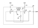
- FIG. 4 is a circuit diagram illustrating a configuration example of the RC oscillation circuit 250 according to the first embodiment of the present technology.
- the RC oscillation circuit 250 includes an inverter 251, a delay circuit 252, and a buffer amplifier 255.
- the delay circuit 252 includes a capacitor 253 and a resistor 254.
- the inverter 251 inverts the signal fed back from the buffer amplifier 255 using the temperature compensation voltage VDD2.
- the inverter 251 supplies the inverted signal to the delay circuit 252 as the inverted signal INV.
- the inverter 251 is an example of the inverting element described in the claims.
- the delay circuit 252 delays the inverted signal INV and outputs it to the buffer amplifier 255 as a delay signal.
- the buffer amplifier 255 outputs a delay signal as a clock signal CLK to the counter circuit 290 using the temperature compensation voltage VDD1, and feeds it back to the inverter 251.
- the buffer amplifier 255 is an example of an output unit described in the claims.
- one end of the capacitor 253 is connected to the output terminal of the inverter 251, and the other end is connected to the resistor 254 and the input terminal of the buffer amplifier 255.
- One end of the resistor 254 is connected to the input terminal of the buffer 253 and the buffer amplifier 255, and the other end is connected to the output terminal of the buffer amplifier 255 and the input terminal of the inverter 251.
- FIG. 5 is a graph illustrating an example of the temperature characteristic of the time constant of the RC oscillation circuit 250 according to the first embodiment of the present technology.
- the vertical axis in the figure is a time constant, and the horizontal axis is temperature.
- the time constant of the RC oscillation circuit 250 is represented by RC when the resistance value of the resistor 254 is R and the capacitance of the capacitor 253 is C. Since the resistance value R and the capacitance C vary depending on the temperature, the time constant RC also varies depending on the temperature. Assuming that the resistance value R depends on the temperature while the capacitance C is constant without depending on the temperature, the time constant RC at a certain measurement temperature is expressed by the following equation, for example.
- R 0 is the resistance value of the resistor 254 at a predetermined reference temperature.
- k is a temperature coefficient.
- the unit of resistance value is, for example, ohms, and the unit of capacitance is, for example, farad (F).
- the unit of the time constant RC is, for example, second (s).
- Equation 9 the time constant RC of the RC oscillation circuit 250 becomes longer as the temperature becomes higher.
- the time constant RC may become shorter as the temperature becomes higher.
- R depends on temperature.
- R 0 C in Equation 9 may be replaced with RC 0 .
- C 0 is a capacitance at a predetermined reference temperature.
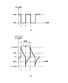
- FIG. 6 is a timing chart illustrating an example of operations of the inverter 251 and the RC oscillation circuit 250 according to the first embodiment of the present technology.
- a in the figure is a timing chart showing an example of the operation of the inverter 251.
- B in the figure is a timing chart showing an example of the operation of the RC oscillation circuit 250.
- the vertical axis of b indicates the input voltage of the buffer amplifier 255, and the horizontal axis indicates time.
- the inverter 251 Inverts the clock signal CLK and outputs an inverted signal INV of a predetermined reference voltage (for example, the ground voltage GND).
- the capacitor 253 starts discharging due to the decrease of the inversion signal INV.
- V TH is a threshold voltage of the transistor in the buffer amplifier 255.
- the inverter 251 inverts the clock signal CLK and outputs an inverted signal INV of the temperature compensation voltage VDD2.
- the capacitor 253 starts to be charged by the rise of the inversion signal INV.
- Equation 10 Substituting Equations 13 and 14 into Equation 10 yields:
- the delay times of the inverter 251 and the buffer amplifier 255 are also included in the period. Considering these delay times, the period is expressed by the following equation.
- dt is the total delay time of each of the inverter 251 and the buffer amplifier 255.
- Equation 19 When the second term of Equation 19 is approximated using the Macrolin's theorem, the following equation is obtained.
- Equation 20 can be approximated by:
- the temperature compensation circuit 220 supplies the temperature compensation voltages VDD1 and VDD2 having a smaller voltage ratio VDD2 / VDD1 as the temperature increases.
- the temperature characteristic of this voltage ratio is opposite to the temperature characteristic of the time constant RC.
- the period T CLK of the RC oscillation circuit 250 is a value corresponding to the voltage ratio VDD2 / VDD1 and the time constant RC from Equation 16. Therefore, by setting m that satisfies Expression 23, the temperature term of Expression 21 can be set to “0” and temperature compensation can be performed for the period TCLK .
- the temperature compensation circuit 220 can also supply the temperature compensation voltages VDD1 and VDD2 having a larger voltage ratio VDD2 / VDD1 as the temperature becomes higher.
- the temperature compensation circuit 220 compensates the temperature of the RC oscillation circuit 250, so that it is possible to reduce the number of parts and cost compared to the case of using a crystal oscillator while accurately measuring the time. it can.
- the temperature compensation voltage VDD1 is constant to simplify the calculation
- the temperature compensation voltage VDD2 may be constant depending on the temperature characteristics of the time constant, and both the temperature compensation voltages VDD1 and VDD2 depend on the temperature. It may be a configuration.
- the temperature compensation circuit 220 may generate the temperature compensation voltages VDD1 and VDD2 whose voltage ratio is expressed by the following expression.
- VDD2 / VDD1 (VDD2 0 / VDD1 0 ) (1 + m ⁇ dT) (24)
- VDD2 0 and VDD 1 0 is a constant value.
- equation 24 is substituted into equation 16, and a temperature coefficient m satisfying the following equation may be set so that the temperature term becomes “0”.
- FIG. 7 is a flowchart illustrating an example of the operation of the communication module 100 according to the first embodiment of the present technology. This operation starts, for example, when the communication module 100 is powered on.
- the temperature compensation circuit 220 generates the temperature compensation voltage VDD2 together with the temperature compensation voltage VDD1 (step S901).
- the RC oscillation circuit 250 generates the clock signal CLK using these voltages (step S902).
- the counter circuit 290 measures time in synchronization with the clock signal (step S903).
- the communication processing unit 110 performs predetermined communication processing based on the timer value (step S904). After step S904, the communication module 100 repeatedly executes step S904.
- the RC oscillation circuit 250 delays the inversion signal by the delay time corresponding to the time constant and the voltage ratio with the time constant and the reverse temperature characteristic.
- a clock signal having a period independent of temperature can be generated.
- the clock signal CLK is generated by the single inverter 251 and the buffer amplifier 255.
- the buffer amplifier 255 is replaced with a two-stage inverter, and VDD2 and the subsequent stage are replaced with the preceding stage.
- VDD1 can be supplied.
- the RC oscillation circuit 250 according to the second embodiment is different from the first embodiment in that the buffer amplifier 255 is replaced with a two-stage inverter and VDD1 and VDD2 are supplied.
- FIG. 8 is a circuit diagram showing a configuration example of the RC oscillation circuit 250 according to the second embodiment of the present technology.
- the RC oscillation circuit 250 of the second embodiment is different from the first embodiment in that an output unit 260 is provided instead of the buffer amplifier 255.
- the output unit 260 includes inverters 261 and 262.
- Inverter 261 inverts the signal delayed by capacitor 253 and resistor 254 and outputs the result to inverter 262.
- Inverter 262 inverts the signal from inverter 261 and outputs the inverted signal as clock signal CLK.
- the temperature compensation voltage VDD2 is supplied to the inverters 251 and 261, and the temperature compensation voltage VDD1 is supplied to the inverter 262.
- the inverter 261 is an example of a front-stage inverting element described in the claims, and the inverter 262 is an example of a rear-stage inverting element described in the claims.
- the clock signal CLK generated by the buffer amplifier 255 using the temperature compensation voltage VDD1 is fed back to the inverter 251 as it is.
- the temperature compensation voltage VDD1 is very low compared to the temperature compensation voltage VDD2
- the high level voltage of the clock signal CLK becomes less than the threshold voltage of the transistor in the inverter 251, and the oscillation operation becomes unstable.
- a level shifter may be provided between the buffer amplifier 255 and the inverter 251 to increase the voltage of the clock signal CLK to a threshold voltage or higher.
- the RC oscillation circuit 250 of the third embodiment differs from the first embodiment in that the voltage of the clock signal CLK is converted by a level shifter.
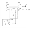
- FIG. 9 is a circuit diagram illustrating a configuration example of the RC oscillation circuit 250 according to the third embodiment of the present technology.
- the RC oscillation circuit 250 of the third embodiment is different from that of the first embodiment in that it further includes a level shifter 270.
- the level shifter 270 converts the voltage of the clock signal CLK.
- This level shifter 270 includes inverters 271 and 272.
- the inverter 271 inverts the clock signal CLK from the buffer amplifier 255 using the temperature compensation voltage VDD1 and supplies the inverted signal to the inverter 272.
- the inverter 272 inverts the signal from the inverter 271 using the temperature compensation voltage VDD2, and supplies the inverted signal to the inverter 251. Thereby, the voltage of the clock signal CLK is converted.
- a level shifter 270 can be added similarly.
- the level shifter 270 converts the voltage of the clock signal CLK, even if the temperature compensation voltage VDD1 is very small compared to the temperature compensation voltage VDD2,
- the RC oscillation circuit 250 can be oscillated.
- the temperature compensation is performed with the parameter a being constant in Expression 16.
- the threshold voltage V TH may vary depending on the manufacturing process and temperature of the pMOS transistor and the nMOS transistor in the inverter 251.
- the parameter a is not constant, and the temperature cannot be sufficiently compensated for the period.
- the RC oscillation circuit 250 of the fourth embodiment is different from that of the first embodiment in that the change of the cycle T CLK caused by the fluctuation of the threshold voltage V TH is suppressed.
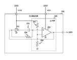
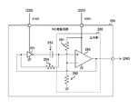
- FIG. 10 is a circuit diagram illustrating a configuration example of the RC oscillation circuit 250 according to the fourth embodiment of the present technology.
- the RC oscillation circuit 250 of the fourth embodiment differs from the first embodiment in that an output unit 280 is provided instead of the buffer amplifier 255.
- the output unit 280 includes resistors 281 and 282 and a comparator 283.
- the resistors 281 and 282 are connected in series between a power supply terminal to which the temperature compensation voltage VDD2 is applied and a ground terminal.
- the connection point between the resistors 281 and 282 is connected to the inverting input terminal ( ⁇ ) of the comparator 283.
- the non-inverting input terminal (+) of the comparator 283 is connected to the capacitor 253 and the resistor 254, and the output terminal of the comparator 283 is connected to the input terminal of the inverter 251, the resistor 254, and the counter circuit 290.
- the comparator 283 is supplied with the temperature compensation voltage VDD1, and the inverter 251 is supplied with the temperature compensation voltage VDD2.
- the temperature compensation voltage VDD2 is divided by the resistors 281 and 282 at a predetermined voltage dividing ratio.
- the circuit composed of the resistors 281 and 282 is an example of a voltage dividing unit described in the claims.
- the comparator 283 compares the voltage of the inverting input terminal ( ⁇ ) (that is, the divided voltage) with the voltage of the non-inverting input terminal (+), and outputs a signal of the comparison result as the clock signal CLK.
- the period T CK is expressed by Equation 26.
- the voltage that the comparator 283 compares with the delay signal is a divided voltage of the temperature compensation voltage VDD2.
- the threshold voltage of the parameter a is replaced with the divided voltage value of the temperature compensation voltage VDD2
- the value of the parameter a becomes equal to the voltage dividing ratio by the resistors 281 and 282. That is, the parameter a is a constant value that does not depend on the process or temperature. Therefore, it is possible to suppress a change in the period TCLK due to a variation in threshold voltage.
- VDD1 may be divided and supplied to the comparator 283 instead of the temperature compensation voltage VDD2.
- the period T CK is expressed by Expression 17.
- the comparator 283 compares the delay signal with the divided voltage of the temperature compensation voltage VDD1 and outputs the clock signal, so that the clock signal caused by the fluctuation of the threshold voltage is output. A change in the period can be suppressed.
- the processing procedure described in the above embodiment may be regarded as a method having a series of these procedures, and a program for causing a computer to execute these series of procedures or a recording medium storing the program. You may catch it.
- a recording medium for example, a CD (Compact Disc), an MD (MiniDisc), a DVD (Digital Versatile Disc), a memory card, a Blu-ray disc (Blu-ray (registered trademark) Disc), or the like can be used.
- this technique can also take the following structures.
- a temperature compensation circuit that generates two temperature compensation voltages whose voltage ratio depends on temperature;
- An inverting element that inverts a feedback signal using one of the two temperature compensation voltages and outputs the inverted signal as an inverted signal;
- a delay circuit that delays the inverted signal over a delay time corresponding to a time constant that is opposite to the voltage ratio and the voltage ratio, and outputs the inverted signal as a delayed signal;
- An oscillation circuit comprising: an output unit that outputs the delayed signal as a periodic signal using the other of the two temperature compensation voltages and feeds it back as the feedback signal.
- the delay circuit includes a capacitor and a resistor, One end of the capacitor is connected to the output terminal of the inverting element, the other end is connected to the resistor and the output unit, The oscillation circuit according to (1), wherein one end of the resistor is connected to the capacitor and the output unit.
- the output unit comprises a buffer amplifier, The oscillation circuit according to (2), wherein the other end of the resistor is connected to an input terminal of the inverting element and an output terminal of the buffer amplifier.
- the output unit A pre-stage inverting element that inverts the delayed signal and outputs it as an internal signal; A rear stage inverting element that inverts the internal signal and outputs it as the feedback signal; The other end of the resistor is connected to the input terminal of the inverting element and the output terminal of the post-stage inverting element, One of the two temperature compensation voltages is supplied to the inverting element and the preceding-stage inverting element, The oscillation circuit according to (2), wherein the second-stage inverting element is supplied with the other of the two temperature compensation voltages.
- the output unit A comparator that compares the voltage of the inverting input terminal with the voltage of the non-inverting input terminal and feeds back a signal indicating the comparison result as the feedback signal; A voltage dividing unit that divides one of the two temperature compensation voltages and supplies the divided voltage to the inverting input terminal; The other end of the resistor is connected to the output terminal of the comparator and the input terminal of the inverting element, The oscillation circuit according to (2), wherein the other end of the capacitor is connected to the non-inverting input terminal.
- (6) further comprising a level shifter that converts the voltage of the feedback signal using the two temperature compensation voltages and outputs the converted voltage to the inverting element;
- the oscillation circuit according to any one of (1) to (5), wherein the output unit outputs the feedback signal to the level shifter.
- a temperature compensation circuit that generates two temperature compensation voltages whose voltage ratio depends on temperature;
- An inverting element that inverts a feedback signal using one of the two temperature compensation voltages and outputs the inverted signal as an inverted signal;
- a delay circuit that delays the inverted signal over a delay time corresponding to a time constant that is opposite to the voltage ratio and the voltage ratio, and outputs the inverted signal as a delayed signal;
- An output unit that outputs the delayed signal as a periodic signal using the other of the two temperature compensation voltages and feeds it back as the feedback signal;
- a timer circuit comprising a counter circuit for counting a count value in synchronization with the periodic signal.
- a temperature compensation circuit that generates two temperature compensation voltages whose voltage ratio depends on temperature;
- An inverting element that inverts a feedback signal using one of the two temperature compensation voltages and outputs the inverted signal as an inverted signal;
- a delay circuit that delays the inverted signal over a delay time corresponding to a time constant that is opposite to the voltage ratio and the voltage ratio, and outputs the inverted signal as a delayed signal;
- An output unit that outputs the delayed signal as a periodic signal using the other of the two temperature compensation voltages and feeds it back as the feedback signal;
- a counter circuit for counting a count value in synchronization with the periodic signal;
- An electronic apparatus comprising: a processing unit that executes a predetermined process based on the count value.
- (9) a temperature compensation voltage generation procedure for generating two temperature compensation voltages whose voltage ratio depends on temperature;
- An inversion procedure for inverting the feedback signal using one of the two temperature compensation voltages and outputting it as an inverted signal;
- An oscillation circuit control method comprising: an output procedure for outputting the delayed signal as a periodic signal using the other of the two temperature compensation voltages and returning the delayed signal as the feedback signal.
Landscapes
- Pulse Circuits (AREA)
- Inductance-Capacitance Distribution Constants And Capacitance-Resistance Oscillators (AREA)
- Oscillators With Electromechanical Resonators (AREA)
Abstract
抵抗およびコンデンサを用いる発振回路において、周期が温度に依存しない周期信号を生成する。 温度補償回路は、電圧比が温度に依存する2つの温度補償電圧を生成する。反転素子は、2つの温度補償電圧の一方を用いて帰還信号を反転して反転信号として出力する。遅延回路は、温度特性が前記電圧比と逆の時定数と電圧比とに応じた遅延時間に亘って反転信号を遅延させて遅延信号として出力する。出力部は、2つの温度補償電圧の他方を用いて遅延信号を周期信号として出力するとともに帰還信号として帰還させる。
Description
本技術は、発振回路、計時回路、電子機器および発振回路の制御方法に関する。詳しくは、抵抗およびコンデンサを用いる発振回路、計時回路、電子機器および発振回路の制御方法に関する。
従来より、タイマなどの回路において、周期信号を生成するために、抵抗およびコンデンサを含む発振回路が用いられている。例えば、可変抵抗およびコンデンサとインバータとを接続した発振回路の抵抗値を制御することにより、周期信号の周期を調整するクロック制御回路が提案されている(例えば、特許文献1参照。)。
上述の従来技術では、時定数RCに応じた周期の周期信号を生成することができる。ここで、Rは可変抵抗の抵抗値であり、Cはコンデンサの静電容量である。しかしながら、RやCは、温度の変化に応じて値が変動するため、周期信号の周期が温度に依存して変動してしまうという問題がある。温度センサで温度を測定し、測定温度に応じて抵抗値を補正する方法も考えられるが、温度センサや補正値を演算する回路を追加する必要があり、回路規模やコストが増大するおそれがある。
本技術はこのような状況に鑑みて生み出されたものであり、抵抗およびコンデンサを用いる発振回路において、周期が温度に依存しない周期信号を生成することを目的とする。
本技術は、上述の問題点を解消するためになされたものであり、その第1の側面は、電圧比が温度に依存する2つの温度補償電圧を生成する温度補償回路と、上記2つの温度補償電圧の一方を用いて帰還信号を反転して反転信号として出力する反転素子と、温度特性が上記電圧比と逆の時定数と上記電圧比とに応じた遅延時間に亘って上記反転信号を遅延させて遅延信号として出力する遅延回路と、上記2つの温度補償電圧の他方を用いて上記遅延信号を周期信号として出力するとともに上記帰還信号として帰還させる出力部とを具備する発振回路、および、その制御方法である。これにより、温度特性が電圧比と逆の時定数と電圧比とに応じた遅延時間に亘って反転信号が遅延するという作用をもたらす。
また、この第1の側面において、上記遅延回路は、コンデンサおよび抵抗を備え、上記コンデンサの一端は、上記反転素子の出力端子に接続され、他端は上記抵抗と上記出力部とに接続され、上記抵抗の一端は、上記コンデンサおよび上記出力部に接続されてもよい。これにより、抵抗の抵抗値にコンデンサの静電容量を乗じた時定数と電圧比とに応じた遅延時間に亘って反転信号が遅延するという作用をもたらす。
また、この第1の側面において、上記出力部は、バッファアンプからなり、上記抵抗の他端は、上記反転素子の入力端子と上記バッファアンプの出力端子とに接続されてもよい。これにより、バッファアンプからの帰還信号が反転素子に帰還するという作用をもたらす。
また、この第1の側面において、上記出力部は、
上記遅延信号を反転して内部信号として出力する前段反転素子と、上記内部信号を反転させて上記帰還信号として出力する後段反転素子とを備え、上記抵抗の他端は、上記反転素子の入力端子と上記後段反転素子の出力端子とに接続され、上記反転素子および上記前段反転素子には上記2つの温度補償電圧の一方が供給され、上記後段反転素子には上記2つの温度補償電圧の他方が供給されてもよい。これにより、反転素子、前段反転素子および後段反転素子の遅延時間に応じた周期で帰還信号が発信するという作用をもたらす。
上記遅延信号を反転して内部信号として出力する前段反転素子と、上記内部信号を反転させて上記帰還信号として出力する後段反転素子とを備え、上記抵抗の他端は、上記反転素子の入力端子と上記後段反転素子の出力端子とに接続され、上記反転素子および上記前段反転素子には上記2つの温度補償電圧の一方が供給され、上記後段反転素子には上記2つの温度補償電圧の他方が供給されてもよい。これにより、反転素子、前段反転素子および後段反転素子の遅延時間に応じた周期で帰還信号が発信するという作用をもたらす。
また、この第1の側面において、上記出力部は、反転入力端子の電圧と非反転入力端子の電圧とを比較して当該比較結果を示す信号を上記帰還信号として帰還させるコンパレータと、上記2つの温度補償電圧の一方を分圧して上記反転入力端子に供給する分圧部と
をさらに具備し、上記抵抗の他端は、上記コンパレータの出力端子と上記反転素子の入力端子とに接続され、上記コンデンサの上記他端は、上記非反転入力端子に接続されてもよい。これにより、2つの温度補償電圧の一方の分圧と、遅延信号とが比較されるという作用をもたらす。
をさらに具備し、上記抵抗の他端は、上記コンパレータの出力端子と上記反転素子の入力端子とに接続され、上記コンデンサの上記他端は、上記非反転入力端子に接続されてもよい。これにより、2つの温度補償電圧の一方の分圧と、遅延信号とが比較されるという作用をもたらす。
また、この第1の側面において、上記2つの温度補償電圧を用いて上記帰還信号の電圧を変換して上記反転素子に出力するレベルシフタをさらに具備し、上記出力部は、上記帰還信号を上記レベルシフタに出力してもよい。これにより、帰還信号の電圧が変換されるという作用をもたらす。
また、本技術の第2の側面は、電圧比が温度に依存する2つの温度補償電圧を生成する温度補償回路と、上記2つの温度補償電圧の一方を用いて帰還信号を反転して反転信号として出力する反転素子と、温度特性が上記電圧比と逆の時定数と上記電圧比とに応じた遅延時間に亘って上記反転信号を遅延させて遅延信号として出力する遅延回路と、上記2つの温度補償電圧の他方を用いて上記遅延信号を周期信号として出力するとともに上記帰還信号として帰還させる出力部と、上記周期信号に同期して計数値を計数するカウンタ回路とを具備する計時回路である。これにより、抵抗の抵抗値にコンデンサの静電容量を乗じた時定数と電圧比とに応じた遅延時間に亘って反転信号が遅延した帰還信号に同期して計数値が計数されるという作用をもたらす。
また、本技術の第3の側面は、電圧比が温度に依存する2つの温度補償電圧を生成する温度補償回路と、上記2つの温度補償電圧の一方を用いて帰還信号を反転して反転信号として出力する反転素子と、温度特性が上記電圧比と逆の時定数と上記電圧比とに応じた遅延時間に亘って上記反転信号を遅延させて遅延信号として出力する遅延回路と、上記2つの温度補償電圧の他方を用いて上記遅延信号を周期信号として出力するとともに上記帰還信号として帰還させる出力部と、上記周期信号に同期して計数値を計数するカウンタ回路と、上記計数値に基づいて所定の処理を実行する処理部とを具備する電子機器である。これにより、抵抗の抵抗値にコンデンサの静電容量を乗じた時定数と電圧比とに応じた遅延時間に亘って反転信号が遅延した帰還信号に同期して計数値が計数され、その計数値に基づいて所定の処理が実行されるという作用をもたらす。
本技術によれば、抵抗およびコンデンサを用いる発振回路において、周期が温度に依存しない周期信号を生成することができるという優れた効果を奏し得る。なお、ここに記載された効果は必ずしも限定されるものではなく、本開示中に記載されたいずれかの効果であってもよい。
以下、本技術を実施するための形態(以下、実施の形態と称する)について説明する。説明は以下の順序により行う。
1. 第1の実施の形態(温度に依存する電圧比を生成する例)
2.第2の実施の形態(インバータを3つ配置し、温度に依存する電圧比を生成する例)
3.第3の実施の形態(電圧を変換し、温度に依存する電圧比を生成する例)
4.第4の実施の形態(温度に依存する電圧比を生成し、温度補償電圧を分圧する例)
1. 第1の実施の形態(温度に依存する電圧比を生成する例)
2.第2の実施の形態(インバータを3つ配置し、温度に依存する電圧比を生成する例)
3.第3の実施の形態(電圧を変換し、温度に依存する電圧比を生成する例)
4.第4の実施の形態(温度に依存する電圧比を生成し、温度補償電圧を分圧する例)
<1.第1の実施の形態>
[通信モジュールの構成例]
図1は、本技術の第1の実施の形態における通信モジュール100の一構成例を示すブロック図である。この通信モジュール100は、BLE(Bluetooth(登録商標) Low Energy)などの通信規格に従って通信処理を行うものであり、例えば、ウェアラブル機器やモバイル機器に搭載される。そして、通信モジュール100は、通信処理部110およびリアルタイムクロック200を備える。また、リアルタイムクロック200は、発振回路210およびカウンタ回路290を備える。
[通信モジュールの構成例]
図1は、本技術の第1の実施の形態における通信モジュール100の一構成例を示すブロック図である。この通信モジュール100は、BLE(Bluetooth(登録商標) Low Energy)などの通信規格に従って通信処理を行うものであり、例えば、ウェアラブル機器やモバイル機器に搭載される。そして、通信モジュール100は、通信処理部110およびリアルタイムクロック200を備える。また、リアルタイムクロック200は、発振回路210およびカウンタ回路290を備える。
リアルタイムクロック200は、通信モジュール100への電源供給が停止している間においても継続して時刻を計時する回路である。このリアルタイムクロック200は、計時した時刻を示すタイマ値を通信処理部110に信号線119を介して供給する。また、リアルタイムクロック200には、バッテリー(不図示)が接続される。そして、通信モジュール100への電源供給の停止中においてリアルタイムクロック200は、バッテリーからの電源を使用して動作する。なお、リアルタイムクロック200は、特許請求の範囲に記載の計時回路の一例である。
発振回路210は、所定周波数の周期信号をクロック信号CLKとして生成するものである。この発振回路210は、温度補償回路220およびRC発振回路250を備える。
温度補償回路220は、温度補償電圧VDD2およびVDD1とを生成してRC発振回路250に供給することにより、温度変化に伴うクロック信号CLKの周期の変動を抑制する(言い換えれば、温度補償を行う)ものである。
温度補償電圧VDD2およびVDD1の電圧比VDD2/VDD1は、温度に依存し、RC発振回路250の時定数と逆の温度特性を有する。温度が高くなるほど時定数が長くなる場合は、これとは逆に、温度が高くなるほど小さな電圧比が設定される。例えば、温度が高くなるほど低い温度補償電圧VDD2と、温度に依存しない一定の温度補償電圧VDD1とが生成される。
RC発振回路250は、抵抗およびコンデンサを用いてクロック信号CLKを生成するものである。このRC発振回路250は、クロック信号CLKをカウンタ回路290に供給する。
カウンタ回路290は、クロック信号CLKに同期して計数値を計数するものである。このカウンタ回路290は、計数値をタイマ値として通信処理部110に供給する。
通信処理部110は、タイマ値に基づいて所定の通信処理を実行するものである。例えば、通信処理部110は、タイマ値を参照して、無線信号を送受信する処理を間欠的に実行する。また、通信処理部110は、外部の装置から正確な時刻情報を取得すると、その時刻情報に基づいてタイマ値を補正する。なお、通信処理部110は、特許請求の範囲に記載の処理部の一例である。
なお、通信モジュール100に発振回路210を設けているが、タイマ値に基づいて動作する機器であれば、通信モジュール100以外の電子機器に発振回路210を設けることもできる。なお、通信モジュール100は、特許請求の範囲に記載の電子機器の一例である。
[温度補償回路の構成例]
図2は、本技術の第1の実施の形態における温度補償回路220の一構成例を示す回路図である。この温度補償回路220は、温度補償電圧供給部230および240を備える。
図2は、本技術の第1の実施の形態における温度補償回路220の一構成例を示す回路図である。この温度補償回路220は、温度補償電圧供給部230および240を備える。
温度補償電圧供給部230は、温度補償電圧VDD2を生成してRC発振回路250に供給するものである。この温度補償電圧供給部230は、定電流源231、pMOS(p-channel Metal-Oxide Semiconductor)トランジスタ232、nMOS(n-channel MOS)トランジスタ233およびオペアンプ234を備える。
pMOSトランジスタ232およびnMOSトランジスタ233は、定電流源231と所定の基準電圧の端子(接地端子など)との間に直列に接続される。また、pMOSトランジスタ232およびnMOSトランジスタ233のそれぞれのゲートは、それらのトランジスタの接続点に接続される。言い換えれば、pMOSトランジスタ232およびnMOSトランジスタ233からなるインバータの入力端子と出力端子とが短絡されている。
オペアンプ234の反転入力端子(-)は、定電流源231およびpMOSトランジスタ232の接続点に接続され、非反転入力端子(+)は、出力端子に接続される。また、オペアンプ234の出力端子は、RC発振回路250にも接続される。
上述の構成により、入出力が短絡されたインバータに定電流源231からの電流を供給して発生した電圧が、オペアンプ234によりバッファリングされて温度補償電圧VDD2として出力される。
また、温度補償電圧供給部240は、定電流源241、pMOSトランジスタ242、nMOSトランジスタ243およびオペアンプ244を備える。これらの素子の接続構成は、温度補償電圧供給部230と同様である。
そして、ある測定温度における温度補償電圧VDD2は、例えば、次の式により表される。
VDD2=VDD20(1-m×dT) ・・・式1
上式において、dTは、所定の基準温度と測定温度との差を示す。温度の単位は、例えば、ケルビン(K)である。mは、温度係数である。温度係数mの設定方法については後述する。VDD20は、基準温度における温度補償電圧を示す。温度補償電圧VDD2の単位は、例えば、ボルト(V)である。
VDD2=VDD20(1-m×dT) ・・・式1
上式において、dTは、所定の基準温度と測定温度との差を示す。温度の単位は、例えば、ケルビン(K)である。mは、温度係数である。温度係数mの設定方法については後述する。VDD20は、基準温度における温度補償電圧を示す。温度補償電圧VDD2の単位は、例えば、ボルト(V)である。
また、pMOSトランジスタ232およびnMOSトランジスタ233は、サブスレッショルド領域で用いられるものとする。この領域において、pMOSトランジスタ232およびnMOSトランジスタ233のドレイン電流IDは、例えば、次の式により表される。

上式において、Kは、ゲート幅とゲート長とのアスペクト比である。また、VGSは、ゲート-ソース間電圧であり、VTHは、トランジスタの閾値電圧である。VTは、熱電圧である。これらの電圧の単位は、例えば、ボルト(V)である。また、イータは、係数である。
また、式2におけるアスペクト比K、I0および熱電圧VTは、次の式により、表される。
K=W/L ・・・式3

VT=kBT/q ・・・式5
K=W/L ・・・式3
式3において、Wは、ゲート幅であり、Lはゲート長である。ゲート幅Wおよびゲート長Lの単位は、例えば、メートル(m)である。式4において、uは、キャリアの移動度であり、単位は、例えば、平方メートル毎ボルト秒(m2/V・s)である。Coxは、酸化膜容量であり、単位は、例えば、ファラッド(F)である。式5においてkBは、ボルツマン定数である。Tは、温度であり、単位は、例えば、ケルビン(K)である。qは、電気素量であり、単位は、例えば、クーロン(C)である。
ここで、定電流源231および241の供給電流をIrefとし、pMOSトランジスタ232および242の閾値電圧をVTHPとし、nMOSトランジスタ233および243の閾値電圧をVTHNとする。また、pMOSトランジスタ232のアスペクト比をpMOSトランジスタ242のM(Mは実数)倍とし、nMOSトランジスタ233のアスペクト比をnMOSトランジスタ243のN(Nは実数)倍とする。この場合、式2に基づいて、温度補償電圧VDD1およびVDD2は、次の式により表される。


式6および式7より、温度補償電圧VDD1およびVDD2の比は、次の式により表される。

式5および式8より、式8におけるMおよびNのパラメータを調整することにより、式1の温度係数mを変更することができる。なお、pMOSトランジスタ232およびnMOSトランジスタ233がサブスレッショルド領域で用いられない場合、式2乃至式8が複雑になるが、同様に、MやNのパラメータの調整により、温度係数mを変更することができる。
なお、式8では、温度が高いほど電圧比VDD2/VDD1を小さくする場合について例示されているが、その逆に温度が高いほど電圧比を大きく設定することもできる。例えば、pMOSトランジスタ242のアスペクト比をpMOSトランジスタ232のM倍とし、nMOSトランジスタ243のアスペクト比をnMOSトランジスタ233のN倍とすればよい。これにより、式8の右辺の第2項の符号が逆になる。
図3は、本技術の第1の実施の形態における温度補償電圧VDD2およびVDD1の比率の温度特性の一例を示すグラフである。同図における縦軸は、VDD2/VDD1の値であり、横軸は温度である。例えば、温度補償電圧VDD2が、式1により表される温度特性を有し、温度補償電圧VDD1が一定である場合、VDD2/VDD1は、温度が高くなるほど、小さな値となる。なお、前述したように、温度が高くなるほど、VDD2/VDD1が大きくなるように設定してもよい。
[RC発振回路の構成例]
図4は、本技術の第1の実施の形態におけるRC発振回路250の一構成例を示す回路図である。このRC発振回路250は、インバータ251、遅延回路252およびバッファアンプ255を備える。また、遅延回路252は、コンデンサ253および抵抗254を備える。
図4は、本技術の第1の実施の形態におけるRC発振回路250の一構成例を示す回路図である。このRC発振回路250は、インバータ251、遅延回路252およびバッファアンプ255を備える。また、遅延回路252は、コンデンサ253および抵抗254を備える。
インバータ251は、バッファアンプ255から帰還した信号を、温度補償電圧VDD2を用いて反転するものである。このインバータ251は、反転した信号を反転信号INVとして遅延回路252に供給する。なお、インバータ251は、特許請求の範囲に記載の反転素子の一例である。
遅延回路252は、反転信号INVを遅延させて遅延信号としてバッファアンプ255に出力するものである。バッファアンプ255は、温度補償電圧VDD1を用いて、遅延信号をクロック信号CLKとしてカウンタ回路290に出力するとともに、インバータ251に帰還させるものである。なお、バッファアンプ255は、特許請求の範囲に記載の出力部の一例である。
遅延回路252において、コンデンサ253の一端は、インバータ251の出力端子に接続され、他端は、抵抗254とバッファアンプ255の入力端子とに接続される。抵抗254の一端は、バッファ253とバッファアンプ255の入力端子とに接続され、他端は、バッファアンプ255の出力端子とインバータ251の入力端子とに接続される。
図5は、本技術の第1の実施の形態におけるRC発振回路250の時定数の温度特性の一例を示すグラフである。同図における縦軸は、時定数であり、横軸は温度である。RC発振回路250の時定数は、抵抗254の抵抗値をRとし、コンデンサ253の静電容量をCとすると、RCにより表される。抵抗値Rや、静電容量Cは、温度に応じて変動するため、時定数RCも温度に応じて変化する。抵抗値Rが温度に依存する一方で静電容量Cが温度に依存せずに一定であると仮定すると、ある測定温度における時定数RCは、例えば、次の式により表される。
RC=R0C(1+k×dT) ・・・式9
上式において、R0は、所定の基準温度における抵抗254の抵抗値である。kは、温度係数である。抵抗値の単位は、例えば、オームであり、静電容量の単位は、例えば、ファラッド(F)である。また、時定数RCの単位は、例えば、秒(s)である。
RC=R0C(1+k×dT) ・・・式9
上式において、R0は、所定の基準温度における抵抗254の抵抗値である。kは、温度係数である。抵抗値の単位は、例えば、オームであり、静電容量の単位は、例えば、ファラッド(F)である。また、時定数RCの単位は、例えば、秒(s)である。
例示した式9では、RC発振回路250の時定数RCは、温度が高くなるほど長くなる。なお、時定数RCは、温度が高くなるほど短くなることもある。また、式9では、抵抗値Rが温度に依存すると仮定したが、抵抗値Rの代わりに静電容量Cが温度に依存する場合は、式9のR0CをRC0に置き換えればよい。C0は、所定の基準温度における静電容量である。
図6は、本技術の第1の実施の形態におけるインバータ251およびRC発振回路250の動作の一例を示すタイミングチャートである。同図におけるaは、インバータ251の動作の一例を示すタイミングチャートである。同図におけるbは、RC発振回路250の動作の一例を示すタイミングチャートである。同図におけるbの縦軸はバッファアンプ255の入力電圧を示し、横軸は時間を示す。
タイミングt0において、クロック信号CLKがハイレベルになると、インバータ251は、そのクロック信号CLKを反転して、所定の基準電圧(例えば、接地電圧GND)の反転信号INVを出力する。反転信号INVの低下により、コンデンサ253は、放電を開始する。
そして、タイミングt0から放電時間T0が経過したタイミングt1において放電が終了し、バッファアンプ255の入力電圧は、VTH-VDD2となる。ここで、VTHは、バッファアンプ255内のトランジスタの閾値電圧である。インバータ251は、クロック信号CLKを反転して、温度補償電圧VDD2の反転信号INVを出力する。反転信号INVの上昇により、コンデンサ253は充電を開始する。
そして、タイミングt1から充電時間T1が経過したタイミングt2において充電が終了し、入力電圧は、VTH+VDD2となる。タイミングt2以降において、入力電圧は、同様の変動を繰り返す。
上述の動作に基づいて、クロック信号CLKの周期TCLKは、次の式により表される。
TCLK=T0+T1 ・・・式10
TCLK=T0+T1 ・・・式10
ここで、時定数に基づいて、放電開始から終了までの入力電圧の変動量は、次の式により表される。

また、充電開始から終了までの入力電圧の変動量は、次の式により表される。

式11および式12を変形すると、次の式が得られる。


式13および式14を式10に代入すると、次の式が得られる。

温度補償電圧VDD1を一定とすると、式15において、VTH/VDD1をパラメータaに置き換えて、次の式が得られる。

ここで、実際には、コンデンサ253の充放電時間の他、インバータ251およびバッファアンプ255のそれぞれの遅延時間も周期に含まれる。これらの遅延時間も考慮すると、周期は、次の式により表される。

上式において、dtは、インバータ251およびバッファアンプ255のそれぞれの遅延時間の合計である。
続いて、式17を用いて温度補償電圧VDD2の温度係数mを設定する方法について説明する。式17においてdtを「0」秒、aを「0.5」とし、式1および式9を式17に代入すると、次の式が得られる。
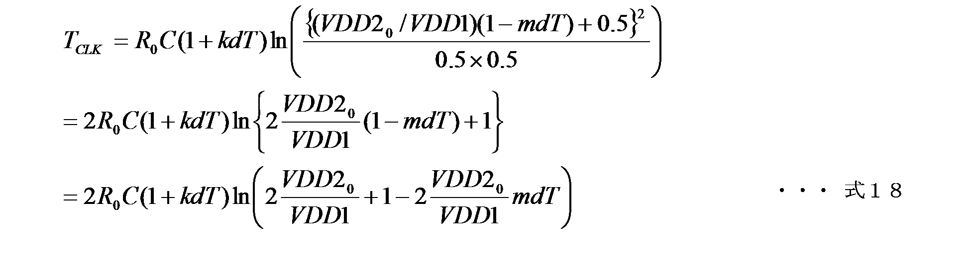
ここで、温度補償電圧VDD1を一定とすると、式18において2×VDD20/VDD1をパラメータAに置き換えて、次の式が得られる。

式19の第2項をマクローリンの定理を用いて近似すると、次の式が得られる。

dT2の項は、非常に小さいものと仮定すると、式20は、次の式に近似することができる。

式21の第2項を「0」にすれば、周期TCLKが温度に依存しなくなる。したがって、次の式を満たす温度係数mを設定すればよい。
kln(A+1)―mA/(1+A)=0 ・・・式22
kln(A+1)―mA/(1+A)=0 ・・・式22
式22を変形すると、次の式が得られる。

前述したように温度補償回路220は、例えば、温度が高くなるほど小さな電圧比VDD2/VDD1の温度補償電圧VDD1およびVDD2を供給する。この電圧比の温度特性は、時定数RCの温度特性と逆の特性である。RC発振回路250の周期TCLKは、式16より、電圧比VDD2/VDD1と時定数RCとに応じた値となる。このため、式23を満たすmの設定により、式21の温度の項を「0」にして周期TCLKについて温度補償を行うことができる。なお、温度補償回路220は、温度が高くなるほど大きな電圧比VDD2/VDD1の温度補償電圧VDD1およびVDD2を供給することもできる。
リアルタイムクロック200などの計時回路では、温度変化により周期が変動すると、時刻が不正確な値となるため、周期は温度依存性を持たないことが求められる。水晶発振器を用いれば、温度変化による周期の変動を許容値以内に抑制することができるが、水晶発振器を用いると、一般にRC発振回路と比べてコストが高くなり、部品点数も増大してしまう。
これに対して、リアルタイムクロック200では、温度補償回路220がRC発振回路250の温度補償を行うため、時刻を正確に計時しつつ、水晶発振器を用いる場合よりも部品点数やコストを削減することができる。
なお、仮に、温度補償電圧VDD1およびVDD2の一方を、インバータ251およびバッファアンプ255の両方に供給すると、温度補償を十分に行うことができなくなる。そのような構成では、充電時の収束波形を放電時と独立して制御することができなくなるためである。
また、計算を簡易化するために温度補償電圧VDD1を一定としていたが、時定数の温度特性によっては温度補償電圧VDD2を一定としてもよいし、温度補償電圧VDD1およびVDD2の両方が温度に依存する構成であってもよい。例えば、温度補償回路220は、電圧比が次の式により表される温度補償電圧VDD1およびVDD2を生成してもよい。
VDD2/VDD1=
(VDD20/VDD10)(1+m×dT)…式24
上式において、VDD20およびVDD10は、一定値である。
VDD2/VDD1=
(VDD20/VDD10)(1+m×dT)…式24
上式において、VDD20およびVDD10は、一定値である。
この場合には式24を式16に代入し、温度の項が「0」になるように、次の式を満たす温度係数mを設定すればよい。

[通信モジュールの動作例]
図7は、本技術の第1の実施の形態における通信モジュール100の動作の一例を示すフローチャートである。この動作は、例えば、通信モジュール100に電源が投入されたときに開始する。
図7は、本技術の第1の実施の形態における通信モジュール100の動作の一例を示すフローチャートである。この動作は、例えば、通信モジュール100に電源が投入されたときに開始する。
温度補償回路220は、温度補償電圧VDD2を温度補償電圧VDD1ともに生成する(ステップS901)。RC発振回路250は、それらの電圧を用いて、クロック信号CLKを生成する(ステップS902)。また、カウンタ回路290は、クロック信号に同期して時刻を計時する(ステップS903)。そして、通信処理部110は、タイマ値に基づいて所定の通信処理を行う(ステップS904)。ステップS904の後に通信モジュール100は、ステップS904を繰り返し実行する。
このように、本技術の第1の実施の形態によれば、RC発振回路250は、時定数と、その時定数と温度特性が逆の電圧比とに応じた遅延時間により反転信号を遅延させるため、温度に依存しない周期のクロック信号を生成することができる。
<2.第2の実施の形態>
上述の第1の実施の形態では、1つのインバータ251とバッファアンプ255等とにより、クロック信号CLKを生成していたが、バッファアンプ255を2段のインバータに置き換えて、その前段にVDD2、後段にVDD1を供給することもできる。これにより、a=VTH/VDD2とすると、周期は、次の式により表される。

この第2の実施の形態のRC発振回路250は、バッファアンプ255を2段のインバータに置き換え、VDD1およびVDD2を供給した点において第1の実施の形態と異なる。
上述の第1の実施の形態では、1つのインバータ251とバッファアンプ255等とにより、クロック信号CLKを生成していたが、バッファアンプ255を2段のインバータに置き換えて、その前段にVDD2、後段にVDD1を供給することもできる。これにより、a=VTH/VDD2とすると、周期は、次の式により表される。
図8は、本技術の第2の実施の形態におけるRC発振回路250の一構成例を示す回路図である。この第2の実施の形態のRC発振回路250は、バッファアンプ255の代わりに出力部260を備える点において第1の実施の形態と異なる。この出力部260は、インバータ261および262を備える。インバータ261は、コンデンサ253および抵抗254で遅延した信号を反転してインバータ262に出力する。インバータ262は、インバータ261からの信号を反転してクロック信号CLKとして出力する。
また、インバータ251および261には、温度補償電圧VDD2が供給され、インバータ262には、温度補償電圧VDD1が供給される。なお、インバータ261は、特許請求の範囲に記載の前段反転素子の一例であり、インバータ262は、特許請求の範囲に記載の後段反転素子の一例である。
インバータ251、261および262の遅延時間の合計が、式26のdtに設定される。
このように、本技術の第2の実施の形態では、インバータ261および262に温度補償電圧VDD2およびVDD1を供給したため、a=VTH/VDD2とすると、式26に示す周期が得られる。
<3.第3の実施の形態>
上述の第1の実施の形態では、温度補償電圧VDD1を用いてバッファアンプ255が生成したクロック信号CLKをそのままインバータ251に帰還させていた。しかし、温度補償電圧VDD1が、温度補償電圧VDD2と比較して非常に低い場合には、クロック信号CLKのハイレベルの電圧が、インバータ251内のトランジスタの閾値電圧未満となり、発振動作が不安定になるおそれがある。このような場合には、バッファアンプ255とインバータ251との間にレベルシフタを設けて、クロック信号CLKの電圧を閾値電圧以上に上昇させればよい。この第3の実施の形態のRC発振回路250は、レベルシフタによりクロック信号CLKの電圧を変換する点において第1の実施の形態と異なる。
上述の第1の実施の形態では、温度補償電圧VDD1を用いてバッファアンプ255が生成したクロック信号CLKをそのままインバータ251に帰還させていた。しかし、温度補償電圧VDD1が、温度補償電圧VDD2と比較して非常に低い場合には、クロック信号CLKのハイレベルの電圧が、インバータ251内のトランジスタの閾値電圧未満となり、発振動作が不安定になるおそれがある。このような場合には、バッファアンプ255とインバータ251との間にレベルシフタを設けて、クロック信号CLKの電圧を閾値電圧以上に上昇させればよい。この第3の実施の形態のRC発振回路250は、レベルシフタによりクロック信号CLKの電圧を変換する点において第1の実施の形態と異なる。
図9は、本技術の第3の実施の形態におけるRC発振回路250の一構成例を示す回路図である。この第3の実施の形態のRC発振回路250は、レベルシフタ270をさらに備える点において第1の実施の形態と異なる。
レベルシフタ270は、クロック信号CLKの電圧を変換するものである。このレベルシフタ270は、インバータ271および272を備える。
インバータ271は、温度補償電圧VDD1を用いてバッファアンプ255からのクロック信号CLKを反転してインバータ272に供給する。インバータ272は、温度補償電圧VDD2を用いて、インバータ271からの信号を反転してインバータ251に供給する。これにより、クロック信号CLKの電圧が変換される。なお、図8に例示した第2の実施の形態のRC発振回路250において、温度補償電圧VDD1が温度補償電圧VDD2と比較して非常に低い場合、同様にレベルシフタ270を追加することができる。
このように、本技術の第3の実施の形態では、レベルシフタ270がクロック信号CLKの電圧を変換するため、温度補償電圧VDD1が温度補償電圧VDD2と比較して非常に小さい場合であっても、RC発振回路250を発振させることができる。
<4.第4の実施の形態>
上述の第1の実施の形態では、式16において、パラメータaを一定として温度補償を行っていた。しかし、実際には、インバータ251内のpMOSトランジスタおよびnMOSトランジスタのそれぞれの製造プロセスや温度に依存して、閾値電圧VTHが変動することがある。閾値電圧VTHが変動すると、パラメータaが一定とならず、周期について温度補償を十分に行うことができない。この第4の実施の形態のRC発振回路250は、閾値電圧VTHの変動に起因する周期TCLKの変化を抑制した点において第1の実施の形態と異なる。
上述の第1の実施の形態では、式16において、パラメータaを一定として温度補償を行っていた。しかし、実際には、インバータ251内のpMOSトランジスタおよびnMOSトランジスタのそれぞれの製造プロセスや温度に依存して、閾値電圧VTHが変動することがある。閾値電圧VTHが変動すると、パラメータaが一定とならず、周期について温度補償を十分に行うことができない。この第4の実施の形態のRC発振回路250は、閾値電圧VTHの変動に起因する周期TCLKの変化を抑制した点において第1の実施の形態と異なる。
図10は、本技術の第4の実施の形態におけるRC発振回路250の一構成例を示す回路図である。この第4の実施の形態のRC発振回路250は、バッファアンプ255の代わりに、出力部280を備える点において第1の実施の形態と異なる。この出力部280は、抵抗281および282とコンパレータ283とを備える。
抵抗281および282は、温度補償電圧VDD2が印加される電源端子と、接地端子との間に直列に接続される。また、抵抗281および282の接続点は、コンパレータ283の反転入力端子(-)に接続される。コンパレータ283の非反転入力端子(+)は、コンデンサ253および抵抗254に接続され、コンパレータ283の出力端子は、インバータ251の入力端子と抵抗254とカウンタ回路290とに接続される。また、コンパレータ283には、温度補償電圧VDD1が供給され、インバータ251には温度補償電圧VDD2が供給される。
抵抗281および282により、温度補償電圧VDD2が所定の分圧比で分圧される。なお、抵抗281および282からなる回路は、特許請求の範囲に記載の分圧部の一例である。
コンパレータ283は、反転入力端子(-)の電圧(すなわち、分圧された電圧)と、非反転入力端子(+)の電圧とを比較して当該比較結果の信号をクロック信号CLKとして出力する。
上述の構成により、a=VTH/VDD2とすると、周期TCKは、式26により表される。また、コンパレータ283が遅延信号と比較する電圧は、温度補償電圧VDD2の分圧となる。このため、パラメータaの閾値電圧を温度補償電圧VDD2の分圧値に置き換えると、パラメータaの値は、抵抗281および282による分圧比と等しくなる。すなわち、パラメータaは、プロセスや温度に依存しない一定値となる。したがって、閾値電圧の変動に起因する周期TCLKの変化を抑制することができる。
なお、第4の実施の形態のRC発振回路250において、第3の実施の形態のレベルシフタ270を追加してもよい。また、図11に例示するように、温度補償電圧VDD2の代わりにVDD1を分圧してコンパレータ283に供給してもよい。この場合には、a=VTH/VDD1として、周期TCKは、式17により表される。
このように本技術の第4の実施の形態では、コンパレータ283が、遅延信号と温度補償電圧VDD1の分圧とを比較してクロック信号を出力するため、閾値電圧の変動に起因するクロック信号の周期の変化を抑制することができる。
なお、上述の実施の形態は本技術を具現化するための一例を示したものであり、実施の形態における事項と、特許請求の範囲における発明特定事項とはそれぞれ対応関係を有する。同様に、特許請求の範囲における発明特定事項と、これと同一名称を付した本技術の実施の形態における事項とはそれぞれ対応関係を有する。ただし、本技術は実施の形態に限定されるものではなく、その要旨を逸脱しない範囲において実施の形態に種々の変形を施すことにより具現化することができる。
また、上述の実施の形態において説明した処理手順は、これら一連の手順を有する方法として捉えてもよく、また、これら一連の手順をコンピュータに実行させるためのプログラム乃至そのプログラムを記憶する記録媒体として捉えてもよい。この記録媒体として、例えば、CD(Compact Disc)、MD(MiniDisc)、DVD(Digital Versatile Disc)、メモリカード、ブルーレイディスク(Blu-ray(登録商標)Disc)等を用いることができる。
なお、本明細書に記載された効果はあくまで例示であって、限定されるものではなく、また、他の効果があってもよい。
なお、本技術は以下のような構成もとることができる。
(1)電圧比が温度に依存する2つの温度補償電圧を生成する温度補償回路と、
前記2つの温度補償電圧の一方を用いて帰還信号を反転して反転信号として出力する反転素子と、
温度特性が前記電圧比と逆の時定数と前記電圧比とに応じた遅延時間に亘って前記反転信号を遅延させて遅延信号として出力する遅延回路と、
前記2つの温度補償電圧の他方を用いて前記遅延信号を周期信号として出力するとともに前記帰還信号として帰還させる出力部と
を具備する発振回路。
(2)前記遅延回路は、コンデンサおよび抵抗を備え、
前記コンデンサの一端は、前記反転素子の出力端子に接続され、他端は前記抵抗と前記出力部とに接続され、
前記抵抗の一端は、前記コンデンサおよび前記出力部に接続される
前記(1)記載の発振回路。
(3)前記出力部は、バッファアンプからなり、
前記抵抗の他端は、前記反転素子の入力端子と前記バッファアンプの出力端子とに接続される
前記(2)記載の発振回路。
(4)前記出力部は、
前記遅延信号を反転して内部信号として出力する前段反転素子と、
前記内部信号を反転させて前記帰還信号として出力する後段反転素子と
を備え、
前記抵抗の他端は、前記反転素子の入力端子と前記後段反転素子の出力端子とに接続され、
前記反転素子および前記前段反転素子には前記2つの温度補償電圧の一方が供給され、
前記後段反転素子には前記2つの温度補償電圧の他方が供給される
前記(2)記載の発振回路。
(5)前記出力部は、
反転入力端子の電圧と非反転入力端子の電圧とを比較して当該比較結果を示す信号を前記帰還信号として帰還させるコンパレータと、
前記2つの温度補償電圧の一方を分圧して前記反転入力端子に供給する分圧部と
をさらに具備し、
前記抵抗の他端は、前記コンパレータの出力端子と前記反転素子の入力端子とに接続され、
前記コンデンサの前記他端は、前記非反転入力端子に接続される
前記(2)記載の発振回路。
(6)前記2つの温度補償電圧を用いて前記帰還信号の電圧を変換して前記反転素子に出力するレベルシフタをさらに具備し、
前記出力部は、前記帰還信号を前記レベルシフタに出力する
前記(1)から(5)のいずれかに記載の発振回路。
(7)電圧比が温度に依存する2つの温度補償電圧を生成する温度補償回路と、
前記2つの温度補償電圧の一方を用いて帰還信号を反転して反転信号として出力する反転素子と、
温度特性が前記電圧比と逆の時定数と前記電圧比とに応じた遅延時間に亘って前記反転信号を遅延させて遅延信号として出力する遅延回路と、
前記2つの温度補償電圧の他方を用いて前記遅延信号を周期信号として出力するとともに前記帰還信号として帰還させる出力部と、
前記周期信号に同期して計数値を計数するカウンタ回路と
を具備する計時回路。
(8)電圧比が温度に依存する2つの温度補償電圧を生成する温度補償回路と、
前記2つの温度補償電圧の一方を用いて帰還信号を反転して反転信号として出力する反転素子と、
温度特性が前記電圧比と逆の時定数と前記電圧比とに応じた遅延時間に亘って前記反転信号を遅延させて遅延信号として出力する遅延回路と、
前記2つの温度補償電圧の他方を用いて前記遅延信号を周期信号として出力するとともに前記帰還信号として帰還させる出力部と、
前記周期信号に同期して計数値を計数するカウンタ回路と、
前記計数値に基づいて所定の処理を実行する処理部と
を具備する電子機器。
(9)電圧比が温度に依存する2つの温度補償電圧を生成する温度補償電圧生成手順と、
前記2つの温度補償電圧の一方を用いて帰還信号を反転して反転信号として出力する反転手順と、
温度特性が前記電圧比と逆の時定数と前記電圧比とに応じた遅延時間に亘って前記反転信号を遅延させて遅延信号として出力する遅延手順と、
前記2つの温度補償電圧の他方を用いて前記遅延信号を周期信号として出力するとともに前記帰還信号として帰還させる出力手順と
を具備する発振回路の制御方法。
(1)電圧比が温度に依存する2つの温度補償電圧を生成する温度補償回路と、
前記2つの温度補償電圧の一方を用いて帰還信号を反転して反転信号として出力する反転素子と、
温度特性が前記電圧比と逆の時定数と前記電圧比とに応じた遅延時間に亘って前記反転信号を遅延させて遅延信号として出力する遅延回路と、
前記2つの温度補償電圧の他方を用いて前記遅延信号を周期信号として出力するとともに前記帰還信号として帰還させる出力部と
を具備する発振回路。
(2)前記遅延回路は、コンデンサおよび抵抗を備え、
前記コンデンサの一端は、前記反転素子の出力端子に接続され、他端は前記抵抗と前記出力部とに接続され、
前記抵抗の一端は、前記コンデンサおよび前記出力部に接続される
前記(1)記載の発振回路。
(3)前記出力部は、バッファアンプからなり、
前記抵抗の他端は、前記反転素子の入力端子と前記バッファアンプの出力端子とに接続される
前記(2)記載の発振回路。
(4)前記出力部は、
前記遅延信号を反転して内部信号として出力する前段反転素子と、
前記内部信号を反転させて前記帰還信号として出力する後段反転素子と
を備え、
前記抵抗の他端は、前記反転素子の入力端子と前記後段反転素子の出力端子とに接続され、
前記反転素子および前記前段反転素子には前記2つの温度補償電圧の一方が供給され、
前記後段反転素子には前記2つの温度補償電圧の他方が供給される
前記(2)記載の発振回路。
(5)前記出力部は、
反転入力端子の電圧と非反転入力端子の電圧とを比較して当該比較結果を示す信号を前記帰還信号として帰還させるコンパレータと、
前記2つの温度補償電圧の一方を分圧して前記反転入力端子に供給する分圧部と
をさらに具備し、
前記抵抗の他端は、前記コンパレータの出力端子と前記反転素子の入力端子とに接続され、
前記コンデンサの前記他端は、前記非反転入力端子に接続される
前記(2)記載の発振回路。
(6)前記2つの温度補償電圧を用いて前記帰還信号の電圧を変換して前記反転素子に出力するレベルシフタをさらに具備し、
前記出力部は、前記帰還信号を前記レベルシフタに出力する
前記(1)から(5)のいずれかに記載の発振回路。
(7)電圧比が温度に依存する2つの温度補償電圧を生成する温度補償回路と、
前記2つの温度補償電圧の一方を用いて帰還信号を反転して反転信号として出力する反転素子と、
温度特性が前記電圧比と逆の時定数と前記電圧比とに応じた遅延時間に亘って前記反転信号を遅延させて遅延信号として出力する遅延回路と、
前記2つの温度補償電圧の他方を用いて前記遅延信号を周期信号として出力するとともに前記帰還信号として帰還させる出力部と、
前記周期信号に同期して計数値を計数するカウンタ回路と
を具備する計時回路。
(8)電圧比が温度に依存する2つの温度補償電圧を生成する温度補償回路と、
前記2つの温度補償電圧の一方を用いて帰還信号を反転して反転信号として出力する反転素子と、
温度特性が前記電圧比と逆の時定数と前記電圧比とに応じた遅延時間に亘って前記反転信号を遅延させて遅延信号として出力する遅延回路と、
前記2つの温度補償電圧の他方を用いて前記遅延信号を周期信号として出力するとともに前記帰還信号として帰還させる出力部と、
前記周期信号に同期して計数値を計数するカウンタ回路と、
前記計数値に基づいて所定の処理を実行する処理部と
を具備する電子機器。
(9)電圧比が温度に依存する2つの温度補償電圧を生成する温度補償電圧生成手順と、
前記2つの温度補償電圧の一方を用いて帰還信号を反転して反転信号として出力する反転手順と、
温度特性が前記電圧比と逆の時定数と前記電圧比とに応じた遅延時間に亘って前記反転信号を遅延させて遅延信号として出力する遅延手順と、
前記2つの温度補償電圧の他方を用いて前記遅延信号を周期信号として出力するとともに前記帰還信号として帰還させる出力手順と
を具備する発振回路の制御方法。
100 通信モジュール
110 通信処理部
200 リアルタイムクロック
210 発振回路
220 温度補償回路
230 温度補償電圧供給部
231、241 定電流源
232、242 pMOSトランジスタ
233、243 nMOSトランジスタ
234、244 オペアンプ
240 温度補償電圧供給部
250 RC発振回路
251、261、262、271、272 インバータ
252 遅延回路
253 コンデンサ
254、281、282 抵抗
255 バッファアンプ
260、280 出力部
270 レベルシフタ
283 コンパレータ
290 カウンタ回路
110 通信処理部
200 リアルタイムクロック
210 発振回路
220 温度補償回路
230 温度補償電圧供給部
231、241 定電流源
232、242 pMOSトランジスタ
233、243 nMOSトランジスタ
234、244 オペアンプ
240 温度補償電圧供給部
250 RC発振回路
251、261、262、271、272 インバータ
252 遅延回路
253 コンデンサ
254、281、282 抵抗
255 バッファアンプ
260、280 出力部
270 レベルシフタ
283 コンパレータ
290 カウンタ回路
Claims (9)
- 電圧比が温度に依存する2つの温度補償電圧を生成する温度補償回路と、
前記2つの温度補償電圧の一方を用いて帰還信号を反転して反転信号として出力する反転素子と、
温度特性が前記電圧比と逆の時定数と前記電圧比とに応じた遅延時間に亘って前記反転信号を遅延させて遅延信号として出力する遅延回路と、
前記2つの温度補償電圧の他方を用いて前記遅延信号を周期信号として出力するとともに前記帰還信号として帰還させる出力部と
を具備する発振回路。 - 前記遅延回路は、コンデンサおよび抵抗を備え、
前記コンデンサの一端は、前記反転素子の出力端子に接続され、他端は前記抵抗と前記出力部とに接続され、
前記抵抗の一端は、前記コンデンサおよび前記出力部に接続される
請求項1記載の発振回路。 - 前記出力部は、バッファアンプからなり、
前記抵抗の他端は、前記反転素子の入力端子と前記バッファアンプの出力端子とに接続される
請求項2記載の発振回路。 - 前記出力部は、
前記遅延信号を反転して内部信号として出力する前段反転素子と、
前記内部信号を反転させて前記帰還信号として出力する後段反転素子と
を備え、
前記抵抗の他端は、前記反転素子の入力端子と前記後段反転素子の出力端子とに接続され、
前記反転素子および前記前段反転素子には前記2つの温度補償電圧の一方が供給され、
前記後段反転素子には前記2つの温度補償電圧の他方が供給される
請求項2記載の発振回路。 - 前記出力部は、
反転入力端子の電圧と非反転入力端子の電圧とを比較して当該比較結果を示す信号を前記帰還信号として帰還させるコンパレータと、
前記2つの温度補償電圧の一方を分圧して前記反転入力端子に供給する分圧部と
をさらに具備し、
前記抵抗の他端は、前記コンパレータの出力端子と前記反転素子の入力端子とに接続され、
前記コンデンサの前記他端は、前記非反転入力端子に接続される
請求項2記載の発振回路。 - 前記2つの温度補償電圧を用いて前記帰還信号の電圧を変換して前記反転素子に出力するレベルシフタをさらに具備し、
前記出力部は、前記帰還信号を前記レベルシフタに出力する
請求項1記載の発振回路。 - 電圧比が温度に依存する2つの温度補償電圧を生成する温度補償回路と、
前記2つの温度補償電圧の一方を用いて帰還信号を反転して反転信号として出力する反転素子と、
温度特性が前記電圧比と逆の時定数と前記電圧比とに応じた遅延時間に亘って前記反転信号を遅延させて遅延信号として出力する遅延回路と、
前記2つの温度補償電圧の他方を用いて前記遅延信号を周期信号として出力するとともに前記帰還信号として帰還させる出力部と、
前記周期信号に同期して計数値を計数するカウンタ回路と
を具備する計時回路。 - 電圧比が温度に依存する2つの温度補償電圧を生成する温度補償回路と、
前記2つの温度補償電圧の一方を用いて帰還信号を反転して反転信号として出力する反転素子と、
温度特性が前記電圧比と逆の時定数と前記電圧比とに応じた遅延時間に亘って前記反転信号を遅延させて遅延信号として出力する遅延回路と、
前記2つの温度補償電圧の他方を用いて前記遅延信号を周期信号として出力するとともに前記帰還信号として帰還させる出力部と、
前記周期信号に同期して計数値を計数するカウンタ回路と、
前記計数値に基づいて所定の処理を実行する処理部と
を具備する電子機器。 - 電圧比が温度に依存する2つの温度補償電圧を生成する温度補償電圧生成手順と、
前記2つの温度補償電圧の一方を用いて帰還信号を反転して反転信号として出力する反転手順と、
温度特性が前記電圧比と逆の時定数と前記電圧比とに応じた遅延時間に亘って前記反転信号を遅延させて遅延信号として出力する遅延手順と、
前記2つの温度補償電圧の他方を用いて前記遅延信号を周期信号として出力するとともに前記帰還信号として帰還させる出力手順と
を具備する発振回路の制御方法。
Priority Applications (1)
| Application Number | Priority Date | Filing Date | Title |
|---|---|---|---|
| JP2019502459A JP7053564B2 (ja) | 2017-03-02 | 2017-11-27 | 発振回路、計時回路、電子機器および発振回路の制御方法 |
Applications Claiming Priority (2)
| Application Number | Priority Date | Filing Date | Title |
|---|---|---|---|
| JP2017038922 | 2017-03-02 | ||
| JP2017-038922 | 2017-03-02 |
Publications (1)
| Publication Number | Publication Date |
|---|---|
| WO2018159033A1 true WO2018159033A1 (ja) | 2018-09-07 |
Family
ID=63369893
Family Applications (1)
| Application Number | Title | Priority Date | Filing Date |
|---|---|---|---|
| PCT/JP2017/042354 Ceased WO2018159033A1 (ja) | 2017-03-02 | 2017-11-27 | 発振回路、計時回路、電子機器および発振回路の制御方法 |
Country Status (2)
| Country | Link |
|---|---|
| JP (1) | JP7053564B2 (ja) |
| WO (1) | WO2018159033A1 (ja) |
Citations (2)
| Publication number | Priority date | Publication date | Assignee | Title |
|---|---|---|---|---|
| JP2002033644A (ja) * | 2000-05-23 | 2002-01-31 | Samsung Electronics Co Ltd | マイクロパワーrc発振器 |
| JP2016133470A (ja) * | 2015-01-22 | 2016-07-25 | セイコーエプソン株式会社 | 回路装置、電子機器、移動体及び物理量検出装置の製造方法 |
-
2017
- 2017-11-27 JP JP2019502459A patent/JP7053564B2/ja active Active
- 2017-11-27 WO PCT/JP2017/042354 patent/WO2018159033A1/ja not_active Ceased
Patent Citations (2)
| Publication number | Priority date | Publication date | Assignee | Title |
|---|---|---|---|---|
| JP2002033644A (ja) * | 2000-05-23 | 2002-01-31 | Samsung Electronics Co Ltd | マイクロパワーrc発振器 |
| JP2016133470A (ja) * | 2015-01-22 | 2016-07-25 | セイコーエプソン株式会社 | 回路装置、電子機器、移動体及び物理量検出装置の製造方法 |
Also Published As
| Publication number | Publication date |
|---|---|
| JPWO2018159033A1 (ja) | 2019-12-26 |
| JP7053564B2 (ja) | 2022-04-12 |
Similar Documents
| Publication | Publication Date | Title |
|---|---|---|
| CN103338026B (zh) | 张弛振荡器 | |
| US11233503B2 (en) | Temperature sensors and methods of use | |
| EP3152538B1 (en) | Low power low cost temperature sensor | |
| JP6415285B2 (ja) | 温度電圧センサ | |
| US9300247B2 (en) | RC oscillator with additional inverter in series with capacitor | |
| EP1971032A2 (en) | Circuit structure of high performance time-to-digital converter | |
| EP4503437A1 (en) | Duty cycle calibration circuit and method, chip, and electronic device | |
| US10361685B2 (en) | Semiconductor device | |
| EP1858163B1 (en) | Oscillator circuit generating oscillating signal having stable cycle | |
| CN114544036B (zh) | 增强型温度传感器 | |
| US20150035550A1 (en) | High accuracy measurement of on-chip component parameters | |
| JP6083503B2 (ja) | 温度周波数変換回路及び温度補償型発振回路 | |
| JP7053564B2 (ja) | 発振回路、計時回路、電子機器および発振回路の制御方法 | |
| CN108123682B (zh) | 振荡装置 | |
| TWI385926B (zh) | 時脈產生器 | |
| CN101609349B (zh) | 时钟产生器 | |
| JP2009236605A (ja) | 温度センサ、温度センサの製造方法、電気泳動装置、および電子機器 | |
| JP6228770B2 (ja) | 充放電型発振回路 | |
| Baek et al. | All-digital time-domain temperature sensor for energy efficient on-chip thermal management | |
| CN104767522A (zh) | 集成电路以及调整所述集成电路的工作周期的方法 | |
| JP2017182183A (ja) | 定電流回路、温度センサーおよび温度補償機能付き時計 | |
| JP5701564B2 (ja) | 半導体集積回路及び測定温度検出方法 | |
| JP2012199604A (ja) | カウンター回路及びそれを内蔵した半導体集積回路 | |
| JP5096248B2 (ja) | ジッタ測定回路 | |
| JPS6318691B2 (ja) |
Legal Events
| Date | Code | Title | Description |
|---|---|---|---|
| 121 | Ep: the epo has been informed by wipo that ep was designated in this application |
Ref document number: 17898703 Country of ref document: EP Kind code of ref document: A1 |
|
| ENP | Entry into the national phase |
Ref document number: 2019502459 Country of ref document: JP Kind code of ref document: A |
|
| NENP | Non-entry into the national phase |
Ref country code: DE |
|
| 122 | Ep: pct application non-entry in european phase |
Ref document number: 17898703 Country of ref document: EP Kind code of ref document: A1 |