WO2018124262A1 - ハードディスク用基板及びそれを用いたハードディスク装置 - Google Patents
ハードディスク用基板及びそれを用いたハードディスク装置 Download PDFInfo
- Publication number
- WO2018124262A1 WO2018124262A1 PCT/JP2017/047169 JP2017047169W WO2018124262A1 WO 2018124262 A1 WO2018124262 A1 WO 2018124262A1 JP 2017047169 W JP2017047169 W JP 2017047169W WO 2018124262 A1 WO2018124262 A1 WO 2018124262A1
- Authority
- WO
- WIPO (PCT)
- Prior art keywords
- hard disk
- substrate
- thickness
- plating
- vickers hardness
- Prior art date
- Legal status (The legal status is an assumption and is not a legal conclusion. Google has not performed a legal analysis and makes no representation as to the accuracy of the status listed.)
- Ceased
Links
Images


Classifications
-
- G—PHYSICS
- G11—INFORMATION STORAGE
- G11B—INFORMATION STORAGE BASED ON RELATIVE MOVEMENT BETWEEN RECORD CARRIER AND TRANSDUCER
- G11B5/00—Recording by magnetisation or demagnetisation of a record carrier; Reproducing by magnetic means; Record carriers therefor
- G11B5/62—Record carriers characterised by the selection of the material
- G11B5/73—Base layers, i.e. all non-magnetic layers lying under a lowermost magnetic recording layer, e.g. including any non-magnetic layer in between a first magnetic recording layer and either an underlying substrate or a soft magnetic underlayer
- G11B5/739—Magnetic recording media substrates
- G11B5/73911—Inorganic substrates
- G11B5/73913—Composites or coated substrates
-
- G—PHYSICS
- G11—INFORMATION STORAGE
- G11B—INFORMATION STORAGE BASED ON RELATIVE MOVEMENT BETWEEN RECORD CARRIER AND TRANSDUCER
- G11B5/00—Recording by magnetisation or demagnetisation of a record carrier; Reproducing by magnetic means; Record carriers therefor
- G11B5/62—Record carriers characterised by the selection of the material
- G11B5/73—Base layers, i.e. all non-magnetic layers lying under a lowermost magnetic recording layer, e.g. including any non-magnetic layer in between a first magnetic recording layer and either an underlying substrate or a soft magnetic underlayer
- G11B5/7368—Non-polymeric layer under the lowermost magnetic recording layer
- G11B5/7371—Non-magnetic single underlayer comprising nickel
-
- G—PHYSICS
- G11—INFORMATION STORAGE
- G11B—INFORMATION STORAGE BASED ON RELATIVE MOVEMENT BETWEEN RECORD CARRIER AND TRANSDUCER
- G11B5/00—Recording by magnetisation or demagnetisation of a record carrier; Reproducing by magnetic means; Record carriers therefor
- G11B5/62—Record carriers characterised by the selection of the material
- G11B5/73—Base layers, i.e. all non-magnetic layers lying under a lowermost magnetic recording layer, e.g. including any non-magnetic layer in between a first magnetic recording layer and either an underlying substrate or a soft magnetic underlayer
- G11B5/7368—Non-polymeric layer under the lowermost magnetic recording layer
- G11B5/7377—Physical structure of underlayer, e.g. texture
-
- G—PHYSICS
- G11—INFORMATION STORAGE
- G11B—INFORMATION STORAGE BASED ON RELATIVE MOVEMENT BETWEEN RECORD CARRIER AND TRANSDUCER
- G11B5/00—Recording by magnetisation or demagnetisation of a record carrier; Reproducing by magnetic means; Record carriers therefor
- G11B5/62—Record carriers characterised by the selection of the material
- G11B5/73—Base layers, i.e. all non-magnetic layers lying under a lowermost magnetic recording layer, e.g. including any non-magnetic layer in between a first magnetic recording layer and either an underlying substrate or a soft magnetic underlayer
- G11B5/739—Magnetic recording media substrates
- G11B5/73911—Inorganic substrates
- G11B5/73917—Metallic substrates, i.e. elemental metal or metal alloy substrates
- G11B5/73919—Aluminium or titanium elemental or alloy substrates
-
- G—PHYSICS
- G11—INFORMATION STORAGE
- G11B—INFORMATION STORAGE BASED ON RELATIVE MOVEMENT BETWEEN RECORD CARRIER AND TRANSDUCER
- G11B5/00—Recording by magnetisation or demagnetisation of a record carrier; Reproducing by magnetic means; Record carriers therefor
- G11B5/84—Processes or apparatus specially adapted for manufacturing record carriers
- G11B5/858—Producing a magnetic layer by electro-plating or electroless plating
Definitions
- the present invention relates to a hard disk substrate and a hard disk device using the same.
- Patent Document 1 describes that the thickness of a magnetic recording substrate using an Al alloy substrate having an outer diameter of 1.89 inches is 0.635 mm and the thickness of the NiP plating layer is 7 ⁇ m or more. ing. And in patent document 2, in order to improve the impact resistance performance of a magnetic disk, it describes that the Vickers hardness of a surface treatment film shall be more than predetermined value.
- the thickness of the Al alloy substrate is reduced, the yield strength of the hard disk substrate is reduced and the hardness is reduced. Therefore, when the magnetic head or the like comes into contact with the hard disk in the hard disk device due to a drop impact or fluttering, the surface of the hard disk is easily damaged.
- the present invention has been made in view of the above points, and the object of the present invention is to provide a thin hard disk substrate capable of suppressing scratches on the disk surface and suppressing surface blurring during rotation. And a hard disk device using the same.
- the hard disk substrate of the present invention that solves the above problems is A hard disk substrate having a NiP plating film formed on the surface of an aluminum alloy substrate,
- the aluminum alloy substrate has a Vickers hardness of 60 Hv or more, the ratio of the plating thickness of the NiP plating film to the plate thickness of the aluminum alloy substrate is 3.8% or more, and the Young's modulus of the hard disk substrate is 74. It is 6 GPa or more, and the hard disk substrate has a Vickers hardness of 293 Hv or more.
- the substrate for hard disk of the present invention is The thickness of the aluminum alloy substrate is 0.338 mm or more and 0.635 mm or less, The plating thickness of the NiP plating film is 22 ⁇ m or more and 60 ⁇ m or less on both sides.
- the present invention also includes a hard disk device using the hard disk substrate.
- the surface of the hard disk is hardly damaged, and the amplitude due to fluttering during rotation of the hard disk can be reduced.
- substrate for hard disks typically.
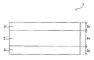
- FIG. 1 is a diagram schematically showing a cross section of a hard disk substrate.
- the hard disk substrate 1 has a configuration in which a NiP plating film 3 which is a non-magnetic surface treatment film is formed on the surface of an aluminum alloy substrate (hereinafter referred to as an Al alloy substrate) 2.
- the NiP plating film 3 is formed on both surfaces of the Al alloy substrate 2.
- the hard disk has a configuration in which a magnetic film is formed on the surface of the hard disk substrate 1.
- the hard disk device is loaded with a plurality of hard disks and includes a motor and a magnetic head.
- the hard disk substrate in the present embodiment is a large-capacity hard disk substrate, and is a magnetic disk substrate having excellent impact resistance and fluttering performance.
- the hard disk substrate has been thinned in recent years, and the number of hard disks mounted in the hard disk device is increasing due to the thinning.
- the recording capacity is increasing in the near-line hard disk application.
- the distance between the surface of the hard disk and the slider surface of the magnetic head has also been made closer, thereby increasing the recording capacity.
- fluttering performance deteriorates when the hard disk rotates in the hard disk device, and the hard disk may flutter, especially when the thickness of the hard disk substrate is 0.635 mm or less. It is.
- the following formula (1) is a formula representing the fluttering performance of the hard disk.
- W F ⁇ a 2 ⁇ (1 ⁇ 2 ) / (E ⁇ ⁇ ⁇ h 3 ⁇ ⁇ 4 ) (1)
- h substrate thickness,
- ⁇ substrate shape parameter
- the hard disk substrate 1 of the present invention has an Al alloy substrate 2 with a Vickers hardness of 60 Hv or more, a ratio of the plating thickness of the NiP plating film 3 to the thickness of the Al alloy substrate 2 of 3.8% or more, and a hard disk
- the Young's modulus of the substrate 1 for a hard disk is 74.6 GPa or more, and the Vickers hardness of the substrate 1 for a hard disk is 293 Hv or more.
- the plating thickness ratio (plating thickness / aluminum thickness (%)), which is the ratio of the plating thickness (b1 + b2) of the NiP plating film 3 and the plate thickness (a1) of the Al alloy substrate 2, is calculated by the following equation (2).
- the sum of the plating thicknesses of the NiP plating films 3 on both surfaces of the hard disk substrate 1 is referred to as “the plating thickness of the NiP plating film 3”, and the NiP plating film on one surface of the hard disk substrate 1.
- the plating thickness 3 is referred to as “one-side plating thickness of the NiP plating film 3”.
- the Al alloy substrate 2 has a thickness of 0.338 mm to 0.635 mm and the NiP plating film 3 has a plating thickness of 22 ⁇ m to 60 ⁇ m. Furthermore, the plating thickness of the NiP plating film 3 is more preferably 22 ⁇ m or more and 40 ⁇ m or less. For example, when the thickness of the Al alloy substrate 2 is 0.617 mm, the plating thickness of the NiP plating film is preferably 22 ⁇ m or more.
- the method for manufacturing a hard disk substrate in the present embodiment includes a substrate forming step in which an Al alloy substrate is ground to form a substrate, and electroless NiP plating is applied to the substrate to form an electroless NiP plating film on the surface of the substrate.
- the plating step includes (1) degreasing treatment, (2) water washing, (3) etching treatment, (4) water washing, (5) desmutting treatment, (6) water washing, and (7) primary zincate.
- the plating solution used for the electroless NiP plating preferably has a high deposition rate and good corrosion resistance.
- the deposition rate is preferably 6.0 ⁇ m / h or more.
- the produced NiP plating film preferably has corrosion resistance with a corrosion area of 1.3% or less when immersed in nitric acid having a concentration of 30% at 40 ° C. for 7 minutes.
- the thickness of the NiP plating film 3 is made larger than when the thickness of the Al alloy substrate is as thick as 0.8 mm, for example. It must be thick. Therefore, if an attempt is made to thicken the plating film using a conventional plating solution having a slow deposition rate, productivity is hindered.
- an Al alloy substrate having a thin plate thickness of 0.635 mm or less is used, but the electroless NiP plating solution uses a material having a high deposition rate as described above. There is no inhibition. Further, although there is a concern that the corrosion resistance is lowered when the deposition rate is increased, in the present embodiment, a material having good corrosion resistance is used, and the corrosion resistance is not impaired. Therefore, when a hard disk substrate is used in a hard disk device, the surface of the hard disk is less likely to be scratched, and it is possible to efficiently produce a hard disk substrate that can reduce the amplitude caused by fluttering during rotation of the hard disk. It becomes.
- fluttering amplitude of the substrate
- the strength and strength against a collision with a magnetic head or a part in contact with the disk can be improved.
- the Al alloy substrate used was a total of two types with a thickness of 0.617 mm and Vickers hardness of 60 Hv and 75 Hv.
- double zincate treatment is applied, and (i) a degreasing treatment is performed at 50 ° C. for 2 minutes using a known degreasing solution comprising sodium phosphate and a surfactant, and (ii) sulfuric acid and phosphoric acid are added.
- a primary zincate treatment is carried out at 20 ° C. for 30 seconds using a known alkali zincate treatment solution comprising sodium hydroxide, zinc, iron and its complexing agent, and (v) a solution similar to the desmutting solution is used at 20 ° C.
- Dezincification treatment was performed for 30 seconds
- secondary zincate treatment was performed at 20 ° C. for 30 seconds using the same solution as the primary zincate treatment.
- a water washing treatment was performed between these steps (i) to (vi).
- electroless nickel plating was performed for an arbitrary time using a known malic acid-succinic acid-based electroless nickel plating solution so as to obtain a target film thickness.
- Table 1 shows the measurement results of the ratio (plating thickness ratio) between the thickness of the NiP plating film and the thickness of the Al alloy substrate and the Vickers hardness of the hard disk substrate 1 when the Vickers hardness of the Al alloy substrate is 60 Hv.
- Table 2 shows the ratio (plating thickness ratio) between the thickness of the NiP plating film and the thickness of the Al alloy substrate when the Vickers hardness of the Al alloy substrate is 75 Hv, and the Vickers of the hard disk substrate 1. The measurement result of hardness is shown.
- FIG. 2 is a graph showing the measurement results of Tables 1 and 2.
- the one-side plating thickness is the thickness (one of b1 or b2) of the NiP plating film on one side of the Al alloy substrate 2, and is basically a film on one side of the Al alloy substrate.
- the thickness and the film thickness on the other side are the same value. That is, the plating thickness is twice the one-side plating thickness.
- the substrate was cut into a width of 10 mm and a length of 60 mm, hung at the position of the vibration node by a fine metal wire and resonated at the free end, and Young's modulus E was calculated using equation (5).
- E Young's modulus
- f E bending resonance frequency
- m mass
- L plate length
- w plate width
- t plate thickness
- Table 3 shows the measurement results of the ratio of the thickness of the NiP plating film to the thickness of the Al alloy substrate (plating thickness ratio) and the Young's modulus of the hard disk substrate 1 when the Vickers hardness of the Al alloy substrate is 60 Hv.
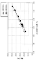
- FIG. 3 is a graph showing the measurement results of Table 3.
- the Young's modulus increases as the plating thickness ratio increases, and the Young's modulus exceeds 74.6 GPa in Examples 8-12 where the plating thickness ratio is 3.82% or more. Fluttering performance has improved dramatically.
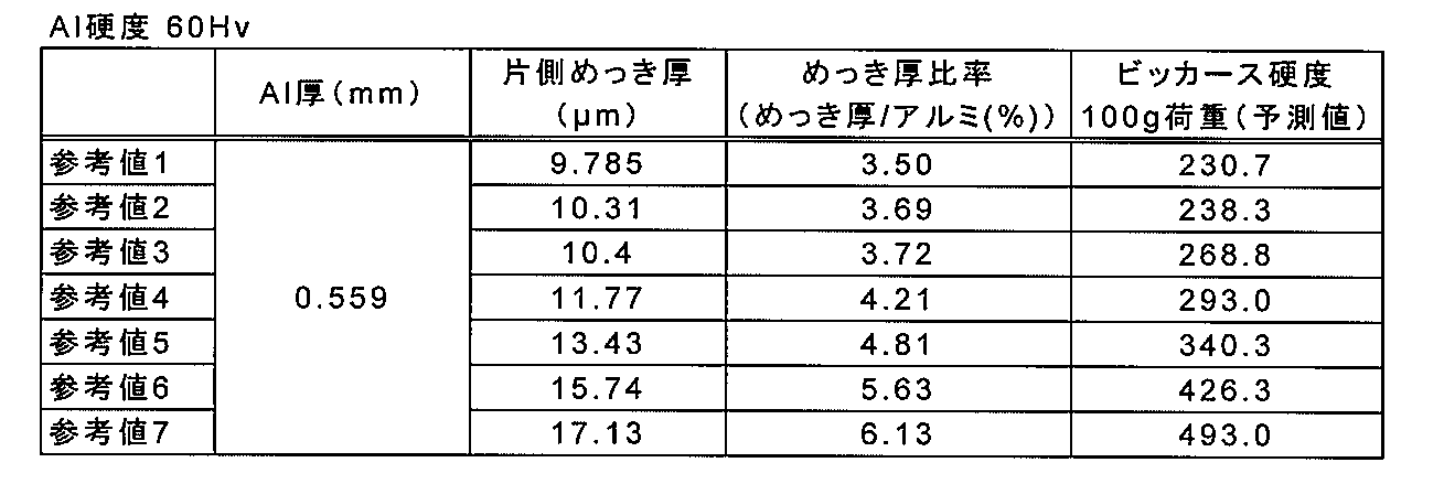
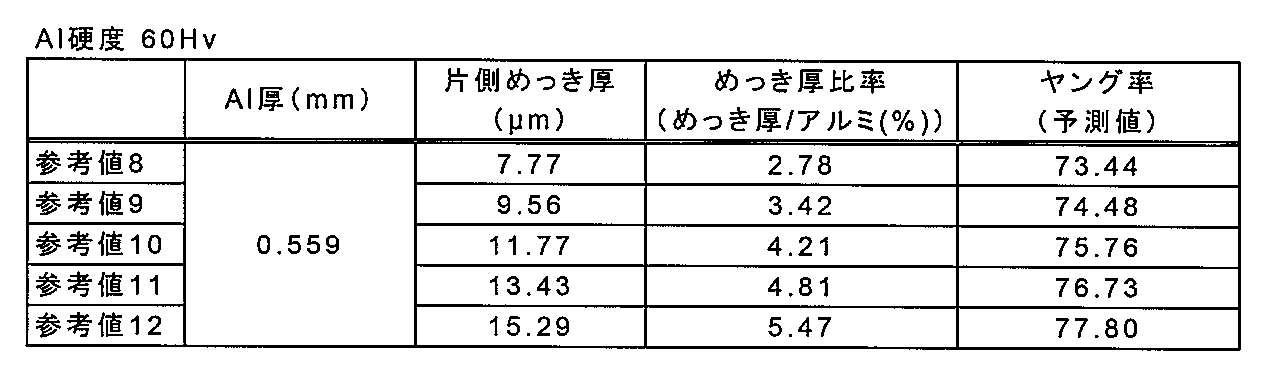
- Tables 4 and 5 show the Vickers hardness and Young's modulus of the hard disk substrate 1 when the thickness of the Al alloy substrate is 0.559 mm and the Vickers hardness of the Al alloy substrate is 60 Hv, and the thickness of the Al alloy substrate is 0.
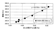
- the numerical value (reference value) calculated by substituting the plating thickness ratio of 0.559 mm for the Al alloy substrate into x in formula (6) created based on the measurement result of .617 mm is shown in FIG. 4 and FIG. 5 are graphs showing the reference values in Tables 4 and 5.
- the reference values shown in Table 4 and Table 5 were calculated based on Example 1-12 and Comparative Example 1-22 shown in Table 1-3.
- the plate thickness of the Al alloy substrate is thinner than that of Example 1-12, so it is preferable to make the one-side plating thickness thicker than that of Example 1-12.
- the reference value 4-7 for Vickers hardness has a high fluttering suppression effect exceeding 293.0 Hv, and the reference value 10-12 for Young's modulus is a high strength material exceeding 75.76 GPa.
- Table 6 shows the measurement results of the Vickers hardness of the hard disk substrate 1 when the thickness of the Al alloy substrate is 0.559 mm and the Vickers hardness of the Al alloy substrate is 60 Hv.
- the hard disk substrate 1 of Example 13 shown in Table 6 has an Al alloy substrate with a one-side plating thickness of 30 ⁇ m and a plating thickness ratio of 10.73.
- the hard disk substrate 1 of Example 13 is a high-strength material having a measurement result of Vickers hardness of 616.0 Hv, and has a higher effect of suppressing the surface from being scratched than each comparative example.
- Table 7 shows the measurement results of the Young's modulus of the hard disk substrate 1 when the thickness of the Al alloy substrate is 0.559 mm and the Vickers hardness of the Al alloy substrate is 60 Hv.
- the hard disk substrate 1 of Example 14 shown in Table 7 has an Al alloy substrate with a one-side plating thickness of 30 ⁇ m and a plating thickness ratio of 10.73.
- the hard disk substrate 1 of Example 14 has a high fluttering suppression effect with a Young's modulus measurement result of 81.3 GPa, and the fluttering performance is dramatically improved as compared with the comparative examples.
- Hard disk substrate 2
- NiP plating film a1
Landscapes
- Engineering & Computer Science (AREA)
- Metallurgy (AREA)
- Chemical & Material Sciences (AREA)
- Inorganic Chemistry (AREA)
- Magnetic Record Carriers (AREA)
- Chemically Coating (AREA)
- Physical Vapour Deposition (AREA)
- Electroplating Methods And Accessories (AREA)
Abstract
本発明の課題は、ディスク表面への傷付きを抑え、回転時の面ブレの発生を抑えることができる薄形のハードディスク用基板及びそれを用いたハードディスク装置を得ることである。本発明のハードディスク用基板1は、アルミニウム合金基板2の表面にNiPめっき膜3が形成されたものであって、アルミニウム合金基板2のビッカース硬度が60Hv以上でかつ、NiPめっき膜3のめっき厚とアルミニウム合金基板2の板厚との比が3.8%以上でかつ、ハードディスク用基板1のヤング率が74.6GPa以上でかつ、ハードディスク用基板1のビッカース硬度が293Hv以上であることを特徴とする。
Description
本発明は、ハードディスク用基板及びそれを用いたハードディスク装置に関する。
ハードディスク装置の大容量化、小型化に伴い、ハードディスク用基板の板厚の薄形化が進んでいる。ハードディスク用基板の厚みを薄くすることで、ハードディスク装置内のハードディスクの積載量(枚数)を増やし、ハードディスク装置の大容量化を図ることができる。
例えば、特許文献1には、外径が1.89インチのAl合金基板を用いた磁気記録用基板の板厚を0.635mmとし、NiPめっき層の膜厚を7μm以上とすることが記載されている。そして、特許文献2では、磁気ディスクの耐衝撃性能を向上させるために、表面処理膜のビッカース硬度を所定値以上とすることが記載されている。
しかしながら、Al合金基板の厚みを薄くすると、ハードディスク装置内でハードディスクが回転したときに面ブレ(フラッタリング)を生じるおそれがある。
また、Al合金基板の厚みを薄くすると、ハードディスク用基板の耐力が低下し、硬度が低下する。したがって、落下の衝撃やフラッタリング等によってハードディスク装置内でハードディスクに磁気ヘッド等が接触した際に、ハードディスクの表面に傷が付きやすくなる。
本発明は、上記の点に鑑みてなされたものであり、その目的とするところは、ディスク表面への傷付きを抑え、回転時の面ブレの発生を抑えることができる薄形のハードディスク用基板及びそれを用いたハードディスク装置を提供することである。
上記課題を解決する本発明のハードディスク用基板は、
アルミニウム合金基板の表面にNiPめっき膜が形成されたハードディスク用基板であって、
前記アルミニウム合金基板のビッカース硬度が60Hv以上でかつ、該NiPめっき膜のめっき厚と前記アルミニウム合金基板の板厚との比が3.8%以上でかつ、前記ハードディスク用基板のヤング率が74.6GPa以上でかつ、前記ハードディスク用基板のビッカース硬度が293Hv以上であることを特徴とする。
アルミニウム合金基板の表面にNiPめっき膜が形成されたハードディスク用基板であって、
前記アルミニウム合金基板のビッカース硬度が60Hv以上でかつ、該NiPめっき膜のめっき厚と前記アルミニウム合金基板の板厚との比が3.8%以上でかつ、前記ハードディスク用基板のヤング率が74.6GPa以上でかつ、前記ハードディスク用基板のビッカース硬度が293Hv以上であることを特徴とする。
本発明のハードディスク用基板は、
前記アルミニウム合金基板の板厚が0.338mm以上0.635mm以下であり、
前記NiPめっき膜のめっき厚が両面併せて22μm以上60μm以下であることを特徴とする。
また、本発明は、上記ハードディスク用基板を用いたハードディスク装置をも含む。
前記アルミニウム合金基板の板厚が0.338mm以上0.635mm以下であり、
前記NiPめっき膜のめっき厚が両面併せて22μm以上60μm以下であることを特徴とする。
また、本発明は、上記ハードディスク用基板を用いたハードディスク装置をも含む。
本発明によれば、かかるハードディスク用基板をハードディスク装置に用いた場合に、ハードディスクの表面に傷が付きにくくなり、ハードディスクの回転時におけるフラッタリングによる振幅を低減させることができる。
本発明に関連する更なる特徴は、本明細書の記述、添付図面から明らかになるものである。また、上記した以外の、課題、構成及び効果は、以下の実施形態の説明により明らかにされる。
次に、本発明の実施の形態について説明する。
図1は、ハードディスク用基板の断面を模式的に示す図である。
図1は、ハードディスク用基板の断面を模式的に示す図である。
ハードディスク用基板1は、アルミニウム合金基板(以下、Al合金基板)2の表面に非磁性な表面処理膜であるNiPめっき膜3が形成された構成を有している。NiPめっき膜3は、Al合金基板2の両面に形成されている。ハードディスクは、ハードディスク用基板1の表面に磁性膜が形成された構成を有している。ハードディスク装置は、複数枚のハードディスクを積載しており、モータや磁気ヘッドを備えている。
本実施の形態におけるハードディスク用基板は、大容量のハードディスク用基板であり、好適な耐衝撃性及びフラッタリング性能に優れた磁気ディスク用基板である。
ハードディスク用基板は近年、薄形化しており、且つ、薄形化によりハードディスク装置に内蔵されるハードディスクの搭載枚数は増加している。特にニアライン向けのハードディスク用途では記録容量が大容量化している。また、ハードディスクの表面と磁気ヘッドのスライダー表面との間の距離も近接化しており、これによる記録容量の大容量化も図られている。
しかしながら、ハードディスクの薄形化に伴い、ハードディスクがハードディスク装置内で回転する際、フラッタリング性能が悪化し、ハードディスクがバタつくおそれがあり、特に、ハードディスク用基板の板厚が0.635mm以下にて顕著である。
下記の式(1)は、ハードディスクのフラッタリング性能を表す式である。
W=F・a2・(1―ν2)/(E・β・h3・λ4) ・・・(1)
W:ハードディスクの振幅、F:基板回転数、a:基板外半径、ν:ポアソン比、E:ヤング率、β:基板のダンピングファクター、h:基板の板厚、λ:基板形状パラメーター
W=F・a2・(1―ν2)/(E・β・h3・λ4) ・・・(1)
W:ハードディスクの振幅、F:基板回転数、a:基板外半径、ν:ポアソン比、E:ヤング率、β:基板のダンピングファクター、h:基板の板厚、λ:基板形状パラメーター
ハードディスクのフラッタリング性能が悪化すると、ハードディスクの表面に対する磁気ヘッドやディスクと接する部位との衝突回数が増加し、例えば、衝突によりハードディスクの保護膜あるいは磁性膜を破壊し、データの信頼性が劣化する。従って、ハードディスク用基板としては、ヤング率を向上させ、フラッタリング(基板の振幅)を低減させ、且つ、磁気ヘッドやディスクと接する部位との衝突に対する強度向上として、耐力や、硬度を高めることが必要である。
本発明のハードディスク用基板1は、Al合金基板2のビッカース硬度が60Hv以上でかつ、NiPめっき膜3のめっき厚とAl合金基板2の板厚との比が3.8%以上でかつ、ハードディスク用基板1のヤング率が74.6GPa以上でかつ、ハードディスク用基板1のビッカース硬度が293Hv以上である。
NiPめっき膜3のめっき厚(b1+b2)とAl合金基板2の板厚(a1)との比であるめっき厚比率(めっき厚/アルミ厚(%))は、下記の式(2)によって算出される。
((b1+b2)÷(a1))×100(%)・・・(2)
((b1+b2)÷(a1))×100(%)・・・(2)
なお、本実施例の説明では、ハードディスク用基板1の両面のNiPめっき膜3のめっき厚を合計した値を「NiPめっき膜3のめっき厚」と称し、ハードディスク用基板1の片面のNiPめっき膜3のめっき厚を「NiPめっき膜3の片側めっき厚」と称する。
ハードディスク用基板1は、Al合金基板2の板厚が0.338mm以上0.635mm以下であり、NiPめっき膜3のめっき厚が22μm以上60μm以下であることが好ましい。さらに、NiPめっき膜3のめっき厚は、22μm以上40μm以下であることがより好ましい。例えば、Al合金基板2の板厚が0.617mmの場合、NiPめっき膜のめっき厚を22μm以上とすることが好ましい。
本実施の形態におけるハードディスク用基板の製造方法は、Al合金基板を研削して基板を形成する基板形成工程と、基板に無電解NiPめっきを施して基板の表面に無電解NiPめっき膜を形成するめっき工程と、無電解NiPめっき膜が形成された基板の表面を研磨する研磨工程と、研磨されためっき皮膜を洗浄する洗浄工程と、を含む。
上記各工程のうち、めっき工程は、(1)脱脂処理、(2)水洗、(3)エッチング処理、(4)水洗、(5)脱スマット処理、(6)水洗、(7)1次ジンケート処理、(8)水洗、(9)脱ジンケート処理、(10)水洗、(11)2次ジンケート処理、(12)水洗、(13)無電解NiPめっき、(14)水洗、(15)乾燥、(16)焼鈍で行うことができる。
上記(13)無電解NiPめっきに用いられるめっき液は、析出速度が早くかつ耐食性が良いものが好ましい。例えば析出速度が6.0μm/h以上であることが好ましい。そして、生成されたNiPめっき皮膜は濃度30%の硝酸に40℃、7分間浸漬した場合に、腐食面積が1.3%以下の耐食性を有するものとなることが好ましい。
ハードディスク用基板を製造する方法において、Al合金基板の板厚を0.635mm以下と薄くする場合、Al合金基板の板厚が例えば0.8mmと厚い場合に比べて、NiPめっき膜3の膜厚をより厚くしなければならない。したがって、従来の析出速度が遅いめっき液を使用してめっき膜を厚くしようとすると生産性を阻害してしまう。
これに対して、本実施の形態では、Al合金基板の板厚が0.635mm以下と薄いものを使用するが、無電解NiPめっき液は上記の析出速度が速いものを使用するので、生産性を阻害することはない。また、析出速度を速めると耐食性が低くなることが懸念されるが、本実施の形態では、耐食性が良いものを使用しており、耐食性が損なわれることはない。したがって、ハードディスク用基板をハードディスク装置に用いた場合に、ハードディスクの表面に傷が付きにくくなり、ハードディスクの回転時におけるフラッタリングによる振幅を低減させることができるハードディスク用基板を効率良く生産することが可能となる。
上記したハードディスク用基板1によれば、フラッタリング(基板の振幅)を低減させ、磁気ヘッドやディスクと接する部位との衝突に対する耐力や、強度を向上させることができる。
[実施例]
<基板の作製>
ビッカース硬度60Hv以上、板厚0.617mmのAl合金基板(JIS H4000に規定された5000系の5086アルミニウム合金)の表面に無電解NiPめっき法を用いて、種々のめっき膜厚の非晶質NiPめっきを施した。
<基板の作製>
ビッカース硬度60Hv以上、板厚0.617mmのAl合金基板(JIS H4000に規定された5000系の5086アルミニウム合金)の表面に無電解NiPめっき法を用いて、種々のめっき膜厚の非晶質NiPめっきを施した。
Al合金基板は、厚みが0.617mmでビッカース硬度が60Hvと75Hvの合計2種類のものを使用した。めっき前処理では、ダブルジンケート処理を適用し、(i)リン酸ソーダ、界面活性剤からなる公知の脱脂液を用いて50℃で2分間の脱脂処理を行い、(ii)硫酸、リン酸を含有する公知のエッチング液を用いて50℃で2分間のエッチング処理を行い、(iii)硝酸を含有する公知の脱スマット液を用いて20℃で30秒間の脱スマット処理を行い、(iv)水酸化ナトリウムと亜鉛と鉄およびその錯化剤からなる公知のアルカリジンケート処理液を用いて20℃で30秒間の一次ジンケート処理を行い、(v)脱スマット液と同様の液を用い20℃で30秒間の脱ジンケート処理を行い、(vi)一次ジンケート処理と同様の液を用い20℃で30秒間の二次ジンケート処理を行った。なお、これら(i)~(vi)の各工程間には水洗処理を実行した。次いで、公知のリンゴ酸-コハク酸系無電解ニッケルめっき液を用い、目的の膜厚になるよう任意の時間、無電解ニッケルめっきを行った。
[評価1:ビッカース硬度]
作製しためっき基板のビッカース硬度を求めるために、ビッカース硬度計((株)アカシ社製、マイクロビッカース硬さ試験機MVK-G2)を使用し、100g荷重で測定を行った。測定方法は、JISZ2244の規定に従って行った。なお、高精度硬さ基準片((株)山本科学工具研究社製、HMV200)で精度を確認しながら測定した。
作製しためっき基板のビッカース硬度を求めるために、ビッカース硬度計((株)アカシ社製、マイクロビッカース硬さ試験機MVK-G2)を使用し、100g荷重で測定を行った。測定方法は、JISZ2244の規定に従って行った。なお、高精度硬さ基準片((株)山本科学工具研究社製、HMV200)で精度を確認しながら測定した。
表1は、Al合金基板のビッカース硬度が60Hvの場合における、NiPめっき膜の膜厚とAl合金基板の板厚との比率(めっき厚比率)と、ハードディスク用基板1のビッカース硬度の測定結果を示すものであり、表2は、Al合金基板のビッカース硬度が75Hvの場合における、NiPめっき膜の膜厚とAl合金基板の板厚との比率(めっき厚比率)と、ハードディスク用基板1のビッカース硬度の測定結果を示すものである。そして、図2は、表1及び表2の測定結果をグラフに示したものである。
なお、表1及び表2において、片側めっき厚とは、Al合金基板2の一方側のNiPめっき膜の膜厚(b1またはb2の一方)であり、基本的にAl合金基板の一方側の膜厚と他方側の膜厚は同じ値となっている。すなわち、片側めっき厚の2倍がめっき厚になる。


めっき厚/アルミ厚の比(めっき厚比率)と、ビッカース硬度との関係式を求めると、下記の式(3)、(4)となる。
Al合金基板のビッカース硬度が60Hv、厚み0.617mmの場合
y=103.79x-97.55 ・・・(3)
Al合金基板のビッカース硬度が75Hv、厚み0.617mmの場合
y=95.307x-44.248 ・・・(4)
Al合金基板のビッカース硬度が60Hv、厚み0.617mmの場合
y=103.79x-97.55 ・・・(3)
Al合金基板のビッカース硬度が75Hv、厚み0.617mmの場合
y=95.307x-44.248 ・・・(4)
(耐衝撃性試験及び評価方法)
上記した実施例1-4のものと比較例3、4、5のものに対して、耐衝撃性試験を行った。耐衝撃性試験では、デュポン社製の衝撃試験器具に罫書き針(トラスコ社製、KB-PK)を装着し、打ち型と受け代の間にディスク用基板を挟み、おもりを落下させて凹みを作り、凹み深さをデジタルマイクロスコープ((株)ハイロックス社製、KH-8700)の3D測定により測定した。
上記した実施例1-4のものと比較例3、4、5のものに対して、耐衝撃性試験を行った。耐衝撃性試験では、デュポン社製の衝撃試験器具に罫書き針(トラスコ社製、KB-PK)を装着し、打ち型と受け代の間にディスク用基板を挟み、おもりを落下させて凹みを作り、凹み深さをデジタルマイクロスコープ((株)ハイロックス社製、KH-8700)の3D測定により測定した。
衝撃値の計算方法を下記に示す。
おもりM:11.9784g
おもり落下高さh:0.05m
打ち具m:13.0840g
停止するまでの時間を0.001sと仮定した場合、
衝撃値『G』=(M/(M+m)×√2gh-止まったときの速度)÷停止するまでの時間(s)=475.2m/s2=48.5G
おもりM:11.9784g
おもり落下高さh:0.05m
打ち具m:13.0840g
停止するまでの時間を0.001sと仮定した場合、
衝撃値『G』=(M/(M+m)×√2gh-止まったときの速度)÷停止するまでの時間(s)=475.2m/s2=48.5G
(評価基準)
凹み深さをそれぞれ異なる箇所で10点測定し、その平均値が120μmより大きいものを耐衝撃性NGである「×」とし、凹み深さの平均値が120μm以下のものを耐衝撃性OKである「○」とした。
凹み深さをそれぞれ異なる箇所で10点測定し、その平均値が120μmより大きいものを耐衝撃性NGである「×」とし、凹み深さの平均値が120μm以下のものを耐衝撃性OKである「○」とした。
(評価結果)
上記した試験の結果、実施例1、2、3、4は、「○」となり、耐衝撃性OKの評価となった。そして、比較例3、4、5は、「×」となり、耐衝撃性NGの評価となった。
表1及び図2に示すように、めっき厚比率が上がるごとにビッカース硬度は向上し、めっき厚比率が3.82%以上となる実施例1-4のものでは、ビッカース硬度が293.0Hvを超える高強度材となった。
上記した試験の結果、実施例1、2、3、4は、「○」となり、耐衝撃性OKの評価となった。そして、比較例3、4、5は、「×」となり、耐衝撃性NGの評価となった。
表1及び図2に示すように、めっき厚比率が上がるごとにビッカース硬度は向上し、めっき厚比率が3.82%以上となる実施例1-4のものでは、ビッカース硬度が293.0Hvを超える高強度材となった。
[評価2:ヤング率]
作製したビッカース硬度60Hvのめっき基板のヤング率を求めるためにヤング率試験装置(日本テクノプラス社製、JE-RT)を用い、室温・大気雰囲気で自由共振法により測定を行った。
作製したビッカース硬度60Hvのめっき基板のヤング率を求めるためにヤング率試験装置(日本テクノプラス社製、JE-RT)を用い、室温・大気雰囲気で自由共振法により測定を行った。
基板は幅10mm、長さ60mmに切断し、金属細線にて振動節の位置に吊るし自由端共振させ、式(5)を用いてヤング率Eを算出した。
 ただし、E:ヤング率、fE:曲げ共振周波数、m:質量、L:板の長さ、w:板の幅、t:板の厚さ
表3はAl合金基板のビッカース硬度が60Hvの場合における、NiPめっき膜の膜厚とAl合金基板の板厚との比率(めっき厚比率)と、ハードディスク用基板1のヤング率の測定結果を示すものであり、図3は、表3の測定結果をグラフに示したものである。

比較例11~比較例20より、めっき厚/アルミ厚の比(めっき厚比率)と、ヤング率との関係式を求めると、下記の式(6)となる。
y=1.6202x+68.935 ・・・(6)
y=1.6202x+68.935 ・・・(6)
表3及び図3に示すように、めっき厚比率が上がるごとにヤング率は向上し、めっき厚比率が3.82%以上の実施例8-12のものでは、ヤング率が74.6GPaを超え、フラッタリング性能が飛躍的に向上した。
表4及び表5は、Al合金基板の板厚が0.559mmでかつAl合金基板のビッカース硬度が60Hvの場合におけるハードディスク用基板1のビッカース硬度及びヤング率を、Al合金基板の板厚が0.617mmの測定結果を元に作成した式(6)に、Al合金基板の板厚が0.559mmのめっき厚比率をxに代入して算出した数値(参考値)を示すものであり、図4及び図5は、表4及び表5の参考値をグラフに示すものである。表4及び表5に示す参考値は、表1-3に示す実施例1-12と比較例1-22に基づいて算出した。
めっき厚比率と、ビッカース硬度(参考値)との関係式を求めると、下記の式(7)となる。
y=95.755x-106.29 ・・・(7)
y=95.755x-106.29 ・・・(7)
そして、めっき厚比率と、ヤング率(参考値)との関係式を求めると、下記の式(8)となる。
y=1.6202x-68.935 ・・・(8)
y=1.6202x-68.935 ・・・(8)
表4及び表5に示すハードディスク用基板1は、実施例1-12よりもAl合金基板の板厚がさらに薄くなっているので、実施例1-12よりも片側めっき厚を厚くするほうが好ましい。ビッカース硬度の参考値4-7は293.0Hvを越えるフラッタリング抑制効果の高いものとなっており、また、ヤング率の参考値10-12は75.76GPaを越える高強度材となっている。
表6は、Al合金基板の板厚が0.559mmでかつAl合金基板のビッカース硬度が60Hvの場合におけるハードディスク用基板1のビッカース硬度の測定結果を示すものである。

表6に示す実施例13のハードディスク用基板1は、Al合金基板の片側めっき厚が30μmであり、めっき厚比率が10.73である。実施例13のハードディスク用基板1は、ビッカース硬度の測定結果が616.0Hvの高強度材となり、各比較例よりも表面が傷付くのを抑制する効果が高いものとなっている。
表7は、Al合金基板の板厚が0.559mmでかつAl合金基板のビッカース硬度が60Hvの場合におけるハードディスク用基板1のヤング率の測定結果を示すものである。

表7に示す実施例14のハードディスク用基板1は、実施例13と同様に、Al合金基板の片側めっき厚が30μmであり、めっき厚比率が10.73である。実施例14のハードディスク用基板1は、ヤング率の測定結果が81.3GPaのフラッタリング抑制効果の高いものとなり、各比較例よりもフラッタリング性能が飛躍的に向上している。
以上、本発明の実施形態について詳述したが、本発明は、前記の実施形態に限定されるものではなく、特許請求の範囲に記載された本発明の精神を逸脱しない範囲で、種々の設計変更を行うことができるものである。
1 ハードディスク用基板
2 アルミニウム合金基板(Al合金基板)
3 NiPめっき膜
a1 アルミニウム合金基板の板厚
b1、b2 NiPめっき膜の膜厚
2 アルミニウム合金基板(Al合金基板)
3 NiPめっき膜
a1 アルミニウム合金基板の板厚
b1、b2 NiPめっき膜の膜厚
Claims (3)
- アルミニウム合金基板の表面にNiPめっき膜が形成されたハードディスク用基板であって、
前記アルミニウム合金基板のビッカース硬度が60Hv以上でかつ、該NiPめっき膜のめっき厚と前記アルミニウム合金基板の板厚との比が3.8%以上でかつ、前記ハードディスク用基板のヤング率が74.6GPa以上でかつ、前記ハードディスク用基板のビッカース硬度が293Hv以上であることを特徴とするハードディスク用基板。 - 前記アルミニウム合金基板の板厚が0.338mm以上0.635mm以下であり、
前記NiPめっき膜のめっき厚が22μm以上60μm以下であることを特徴とする請求項1に記載のハードディスク用基板。 - 請求項1または2に記載のハードディスク用基板を用いたハードディスク装置。
Priority Applications (4)
| Application Number | Priority Date | Filing Date | Title |
|---|---|---|---|
| US16/473,662 US11205453B2 (en) | 2016-12-28 | 2017-12-28 | Hard disk substrate and hard disk device including the hard disk substrate |
| CN201780081695.2A CN110121745B (zh) | 2016-12-28 | 2017-12-28 | 硬盘基片以及使用该硬盘基片的硬盘装置 |
| JP2018559627A JP7122975B2 (ja) | 2016-12-28 | 2017-12-28 | ハードディスク用基板及びそれを用いたハードディスク装置 |
| MYPI2019003396A MY201888A (en) | 2016-12-28 | 2017-12-28 | Hard disk substrate and hard disk device including the hard disk substrate |
Applications Claiming Priority (2)
| Application Number | Priority Date | Filing Date | Title |
|---|---|---|---|
| JP2016-256994 | 2016-12-28 | ||
| JP2016256994 | 2016-12-28 |
Publications (1)
| Publication Number | Publication Date |
|---|---|
| WO2018124262A1 true WO2018124262A1 (ja) | 2018-07-05 |
Family
ID=62709585
Family Applications (1)
| Application Number | Title | Priority Date | Filing Date |
|---|---|---|---|
| PCT/JP2017/047169 Ceased WO2018124262A1 (ja) | 2016-12-28 | 2017-12-28 | ハードディスク用基板及びそれを用いたハードディスク装置 |
Country Status (6)
| Country | Link |
|---|---|
| US (1) | US11205453B2 (ja) |
| JP (1) | JP7122975B2 (ja) |
| CN (1) | CN110121745B (ja) |
| MY (1) | MY201888A (ja) |
| TW (1) | TWI755466B (ja) |
| WO (1) | WO2018124262A1 (ja) |
Cited By (5)
| Publication number | Priority date | Publication date | Assignee | Title |
|---|---|---|---|---|
| CN111383667A (zh) * | 2018-12-28 | 2020-07-07 | 昭和电工株式会社 | 磁记录介质用基板、磁记录介质、硬盘驱动器 |
| JP2022090912A (ja) * | 2020-12-08 | 2022-06-20 | 株式会社Uacj | 磁気ディスク基板および磁気ディスク |
| US11545178B2 (en) | 2017-03-31 | 2023-01-03 | Hoya Corporation | Substrate for magnetic disk and magnetic disk |
| US11694718B2 (en) | 2017-06-30 | 2023-07-04 | Hoya Corporation | Substrate for magnetic disk, magnetic disk, and hard disk drive apparatus |
| US12548595B2 (en) | 2019-09-25 | 2026-02-10 | Western Digital Technologies, Inc. | Magnetic recording apparatus comprising disk with reduced thickness and reduced disk flatness |
Families Citing this family (2)
| Publication number | Priority date | Publication date | Assignee | Title |
|---|---|---|---|---|
| MY208527A (en) | 2018-08-07 | 2025-05-14 | Hoya Corp | Substrate for magnetic disk and magnetic disk |
| US20230335162A1 (en) * | 2022-04-13 | 2023-10-19 | Western Digital Technologies, Inc. | Magnetic recording disk with metallic layers having thicknesses configured to balance weight and rigidity of the disk |
Citations (4)
| Publication number | Priority date | Publication date | Assignee | Title |
|---|---|---|---|---|
| JPH10334445A (ja) * | 1997-06-02 | 1998-12-18 | Kobe Steel Ltd | 磁気ディスク用基板 |
| JP2006241513A (ja) * | 2005-03-02 | 2006-09-14 | Kobe Steel Ltd | 磁気ディスク用アルミニウム合金基板およびその製造方法 |
| WO2012001914A1 (ja) * | 2010-06-30 | 2012-01-05 | コニカミノルタオプト株式会社 | 情報記録媒体用ガラス基板 |
| JP2012195021A (ja) * | 2011-03-15 | 2012-10-11 | Fuji Electric Co Ltd | 磁気記録媒体用基板およびその製造方法 |
Family Cites Families (21)
| Publication number | Priority date | Publication date | Assignee | Title |
|---|---|---|---|---|
| US4826737A (en) * | 1983-04-15 | 1989-05-02 | Mitsubishi Aluminum Kabushiki Kaisha | Method of using aluminum alloy as substrate for magnetic discs with enhanced magnetic recording density |
| JPH087251A (ja) | 1994-06-15 | 1996-01-12 | Fuji Electric Co Ltd | 磁気記録媒体 |
| US5759681A (en) | 1995-02-03 | 1998-06-02 | Hitachi, Ltd. | Magnetic recording medium and magnetic recording system using the same |
| JPH09198640A (ja) | 1996-01-16 | 1997-07-31 | Kobe Steel Ltd | 磁気ディスク |
| JP2000222720A (ja) * | 1999-01-28 | 2000-08-11 | Nikon Corp | 情報記録媒体用基板及び情報記録媒体 |
| US7083871B2 (en) * | 2002-05-09 | 2006-08-01 | Maxtor Corporation | Single-sided sputtered magnetic recording disks |
| JP2007048397A (ja) * | 2005-08-11 | 2007-02-22 | Showa Denko Kk | 磁気記録媒体、その製造方法および磁気記録再生装置 |
| US20100221582A1 (en) * | 2005-12-28 | 2010-09-02 | Hideki Kawai | Magnetic recording medium substrate and magnetic recording medium |
| WO2007119306A1 (ja) * | 2006-03-13 | 2007-10-25 | Konica Minolta Opto, Inc. | 磁気記録媒体用基板、その製造方法、及び磁気記録媒体 |
| JP5325472B2 (ja) * | 2007-09-05 | 2013-10-23 | 株式会社神戸製鋼所 | 磁気ディスク用アルミニウム合金基板およびその製造方法 |
| WO2009096217A1 (ja) * | 2008-01-29 | 2009-08-06 | Konica Minolta Opto, Inc. | 磁気記録媒体用基板の製造方法、及び磁気記録媒体 |
| JP5353715B2 (ja) * | 2008-02-07 | 2013-11-27 | コニカミノルタ株式会社 | 情報記録媒体用ガラス基板の梱包方法 |
| CN102757180B (zh) * | 2008-03-19 | 2016-03-02 | Hoya株式会社 | 磁记录介质基板用玻璃、磁记录介质基板、磁记录介质和它们的制造方法 |
| JP5981841B2 (ja) * | 2012-12-27 | 2016-08-31 | 株式会社神戸製鋼所 | 磁気記録媒体用アルミニウム基板の製造方法 |
| JP6261399B2 (ja) * | 2014-03-17 | 2018-01-17 | 株式会社神戸製鋼所 | 磁気記録媒体用アルミニウム基板 |
| JP5853117B1 (ja) * | 2014-06-30 | 2016-02-09 | 花王株式会社 | 磁気ディスク基板用研磨液組成物 |
| MY182369A (en) | 2014-10-31 | 2021-01-21 | Uacj Corp | Aluminum alloy substrate for magnetic disk |
| JP6646551B2 (ja) * | 2015-12-25 | 2020-02-14 | 昭和電工株式会社 | 磁気記録媒体用基板 |
| JP6574740B2 (ja) * | 2016-07-08 | 2019-09-11 | 昭和電工株式会社 | 磁気記録媒体用基板およびハードディスクドライブ |
| JP6832179B2 (ja) * | 2017-02-03 | 2021-02-24 | 昭和電工株式会社 | 磁気記録媒体用基板およびハードディスクドライブ |
| PH12021552252A1 (en) * | 2017-03-31 | 2022-05-02 | Hoya Corp | Non-magnetic substrate for magnetic disk, and magnetic disk |
-
2017
- 2017-12-27 TW TW106145912A patent/TWI755466B/zh active
- 2017-12-28 CN CN201780081695.2A patent/CN110121745B/zh active Active
- 2017-12-28 WO PCT/JP2017/047169 patent/WO2018124262A1/ja not_active Ceased
- 2017-12-28 MY MYPI2019003396A patent/MY201888A/en unknown
- 2017-12-28 US US16/473,662 patent/US11205453B2/en active Active
- 2017-12-28 JP JP2018559627A patent/JP7122975B2/ja active Active
Patent Citations (4)
| Publication number | Priority date | Publication date | Assignee | Title |
|---|---|---|---|---|
| JPH10334445A (ja) * | 1997-06-02 | 1998-12-18 | Kobe Steel Ltd | 磁気ディスク用基板 |
| JP2006241513A (ja) * | 2005-03-02 | 2006-09-14 | Kobe Steel Ltd | 磁気ディスク用アルミニウム合金基板およびその製造方法 |
| WO2012001914A1 (ja) * | 2010-06-30 | 2012-01-05 | コニカミノルタオプト株式会社 | 情報記録媒体用ガラス基板 |
| JP2012195021A (ja) * | 2011-03-15 | 2012-10-11 | Fuji Electric Co Ltd | 磁気記録媒体用基板およびその製造方法 |
Cited By (8)
| Publication number | Priority date | Publication date | Assignee | Title |
|---|---|---|---|---|
| US11545178B2 (en) | 2017-03-31 | 2023-01-03 | Hoya Corporation | Substrate for magnetic disk and magnetic disk |
| US11955151B2 (en) | 2017-03-31 | 2024-04-09 | Hoya Corporation | Substrate for magnetic disk and magnetic disk |
| US12548594B2 (en) | 2017-03-31 | 2026-02-10 | Hoya Corporation | Substrate for magnetic disk and magnetic disk |
| US11694718B2 (en) | 2017-06-30 | 2023-07-04 | Hoya Corporation | Substrate for magnetic disk, magnetic disk, and hard disk drive apparatus |
| US12190923B2 (en) | 2017-06-30 | 2025-01-07 | Hoya Corporation | Substrate for magnetic disk, magnetic disk, and hard disk drive apparatus |
| CN111383667A (zh) * | 2018-12-28 | 2020-07-07 | 昭和电工株式会社 | 磁记录介质用基板、磁记录介质、硬盘驱动器 |
| US12548595B2 (en) | 2019-09-25 | 2026-02-10 | Western Digital Technologies, Inc. | Magnetic recording apparatus comprising disk with reduced thickness and reduced disk flatness |
| JP2022090912A (ja) * | 2020-12-08 | 2022-06-20 | 株式会社Uacj | 磁気ディスク基板および磁気ディスク |
Also Published As
| Publication number | Publication date |
|---|---|
| TW201841150A (zh) | 2018-11-16 |
| CN110121745A (zh) | 2019-08-13 |
| JPWO2018124262A1 (ja) | 2019-10-31 |
| CN110121745B (zh) | 2021-01-15 |
| JP7122975B2 (ja) | 2022-08-22 |
| US11205453B2 (en) | 2021-12-21 |
| TWI755466B (zh) | 2022-02-21 |
| MY201888A (en) | 2024-03-22 |
| US20190333535A1 (en) | 2019-10-31 |
Similar Documents
| Publication | Publication Date | Title |
|---|---|---|
| WO2018124262A1 (ja) | ハードディスク用基板及びそれを用いたハードディスク装置 | |
| US20180363087A1 (en) | Austenitic stainless steel sheet, cover member and production method for austenitic stainless steel sheet | |
| US20200211595A1 (en) | Substrate for magnetic recording medium, magnetic recording medium, hard disk drive | |
| JPWO2018143177A1 (ja) | アルミニウム合金製の磁気ディスク基板及びその製造方法 | |
| JP2014210968A (ja) | 磁気ディスク用アルミニウム合金基板およびその製造方法 | |
| US11211088B2 (en) | Magnetic disc, aluminum alloy substrate for magnetic disc, and production method for aluminum alloy substrate | |
| US20200211591A1 (en) | Substrate for magnetic recording medium, magnetic recording medium, hard disk drive | |
| US20200211594A1 (en) | Aluminum alloy substrate for magnetic recording medium, substrate for magnetic recording medium, magnetic recording medium, hard disk drive | |
| Mu et al. | Nickel thin film coatings on steels with electroless plating and sputter deposition | |
| CN112002351A (zh) | 磁盘用非磁性基板和磁盘 | |
| JP2010218610A (ja) | 磁気記録媒体及び磁気記憶装置 | |
| Yang et al. | Optimization of Surface Layer Properties of Mg–9Li–1Zn Alloy by Ultrasonic Surface Rolling Process and its Impact on Corrosion Behavior | |
| JP2013208639A (ja) | 洗浄性に優れたステンレス鋼およびその製造方法 | |
| WO2012046712A1 (ja) | ハードディスク用基板の製造方法及びハードディスク用基板 | |
| JP2011134419A (ja) | 磁気記録媒体用ディスク基板及びその製造方法 | |
| JP3182934B2 (ja) | メモリーハードディスクの製造方法 | |
| JP5872322B2 (ja) | 磁気ディスク用基板の製造方法、磁気ディスク用基板、磁気ディスク、磁気ディスク基板用洗浄剤 | |
| JP2006302358A (ja) | 磁気記録媒体用Al合金基板および磁気記録媒体 | |
| WO2012102161A1 (ja) | めっき前処理液及びそれを用いたハードディスク装置用アルミニウム基板の製造方法 | |
| JP2019021368A (ja) | 磁気ディスク用アルミニウム合金基板 | |
| JP6985487B1 (ja) | 磁気ディスク基板および磁気ディスク | |
| WO2013153992A1 (ja) | ハードディスク用基板の製造方法 | |
| JPH0752030A (ja) | 陽極酸化処理基盤及び研磨方法 | |
| CN104513918B (zh) | 水性涂料涂装用铝材 | |
| JPS61267931A (ja) | 磁気デイスク基板の表面処理方法 |
Legal Events
| Date | Code | Title | Description |
|---|---|---|---|
| 121 | Ep: the epo has been informed by wipo that ep was designated in this application |
Ref document number: 17889033 Country of ref document: EP Kind code of ref document: A1 |
|
| ENP | Entry into the national phase |
Ref document number: 2018559627 Country of ref document: JP Kind code of ref document: A |
|
| NENP | Non-entry into the national phase |
Ref country code: DE |
|
| 122 | Ep: pct application non-entry in european phase |
Ref document number: 17889033 Country of ref document: EP Kind code of ref document: A1 |