WO2018124154A1 - 照明装置 - Google Patents
照明装置 Download PDFInfo
- Publication number
- WO2018124154A1 WO2018124154A1 PCT/JP2017/046833 JP2017046833W WO2018124154A1 WO 2018124154 A1 WO2018124154 A1 WO 2018124154A1 JP 2017046833 W JP2017046833 W JP 2017046833W WO 2018124154 A1 WO2018124154 A1 WO 2018124154A1
- Authority
- WO
- WIPO (PCT)
- Prior art keywords
- cover member
- substrate
- led
- lighting device
- mounting
- Prior art date
- Legal status (The legal status is an assumption and is not a legal conclusion. Google has not performed a legal analysis and makes no representation as to the accuracy of the status listed.)
- Ceased
Links
Images


Classifications
-
- F—MECHANICAL ENGINEERING; LIGHTING; HEATING; WEAPONS; BLASTING
- F21—LIGHTING
- F21K—NON-ELECTRIC LIGHT SOURCES USING LUMINESCENCE; LIGHT SOURCES USING ELECTROCHEMILUMINESCENCE; LIGHT SOURCES USING CHARGES OF COMBUSTIBLE MATERIAL; LIGHT SOURCES USING SEMICONDUCTOR DEVICES AS LIGHT-GENERATING ELEMENTS; LIGHT SOURCES NOT OTHERWISE PROVIDED FOR
- F21K9/00—Light sources using semiconductor devices as light-generating elements, e.g. using light-emitting diodes [LED] or lasers
- F21K9/20—Light sources comprising attachment means
- F21K9/27—Retrofit light sources for lighting devices with two fittings for each light source, e.g. for substitution of fluorescent tubes
- F21K9/275—Details of bases or housings, i.e. the parts between the light-generating element and the end caps; Arrangement of components within bases or housings
-
- F—MECHANICAL ENGINEERING; LIGHTING; HEATING; WEAPONS; BLASTING
- F21—LIGHTING
- F21V—FUNCTIONAL FEATURES OR DETAILS OF LIGHTING DEVICES OR SYSTEMS THEREOF; STRUCTURAL COMBINATIONS OF LIGHTING DEVICES WITH OTHER ARTICLES, NOT OTHERWISE PROVIDED FOR
- F21V19/00—Fastening of light sources or lamp holders
-
- H—ELECTRICITY
- H10—SEMICONDUCTOR DEVICES; ELECTRIC SOLID-STATE DEVICES NOT OTHERWISE PROVIDED FOR
- H10H—INORGANIC LIGHT-EMITTING SEMICONDUCTOR DEVICES HAVING POTENTIAL BARRIERS
- H10H20/00—Individual inorganic light-emitting semiconductor devices having potential barriers, e.g. light-emitting diodes [LED]
- H10H20/80—Constructional details
Definitions
- the present invention relates to a lighting device, and more particularly to a straight tube type lighting device using a light emitting diode (LED).
- LED light emitting diode
- a conventional straight-tube LED lighting device is an LED mounting board on which LEDs are arranged and mounted at a predetermined interval, such as aluminum having excellent heat dissipation. What was attached to the elongate base comprised from these metals has the structure accommodated in the inside of resin-made translucent cover members.
- the base on which the LED mounting board is mounted is made of a metal such as aluminum, thereby preventing the lighting device from being greatly deformed when the resin translucent cover member is thermally expanded due to heat generated by the LED. Also have.
- the back surface of the LED mounting board (the surface on the back side of the surface on which the LED is mounted) is the mounting surface to the base, so it cannot be used for wiring.
- the pattern is concentrated only on the surface, that is, only on the LED mounting surface.
- the length is about 60 cm.
- a plurality of LED mounting substrates are connected.
- the connectors and lead wires are connected on the back surface of the LED mounting board. Since it cannot do, it will arrange
- the present invention has been made in view of these points, and an object of the present invention is to provide an illuminating device that easily satisfies safety standards and hardly causes uneven light emission due to light shielding.
- the present invention provides a substrate having a light emitting element mounted on the surface thereof, and a straight tube shape that accommodates the substrate inside and transmits and / or diffuses light emitted from the light emitting element.
- a lighting device comprising a cover member and a long metal member disposed in the cover member, the back surface of the substrate being open toward a cavity in the cover member.
- the “back surface” of a substrate refers to the surface on the back side of the surface on which the light emitting element is mounted on the substrate.
- invention 1 since the back surface of the board
- the connector and the lead wire for connecting the substrates can be disposed on the back surface of the substrate, the light emitted from the light emitting element is not blocked by the connector or the lead wire.
- the long metal member in the cover member it is possible to prevent the lighting device from being greatly deformed when the cover member is thermally expanded due to heat generated by the light emitting element. If it is an illuminating device of such a structure, it will be easy to satisfy
- the cover member is extended in the tube axis direction so that a pair of mounting tables are opposed to each other on the inner peripheral surface of the cover member, and both side ends of the substrate are the pair of mounting tables.
- Invention 2 the cover member is extended in the tube axis direction so that a pair of mounting tables are opposed to each other on the inner peripheral surface of the cover member, and both side ends of the substrate are the pair of mounting tables.
- the substrate can be stably accommodated in the cover member without separately preparing a member for holding the substrate.
- the said elongate member may be inserted in the space in the said cover member separated by the space in which the said board
- a power supply circuit for driving the light emitting element may be mounted on the back surface of the substrate (Invention 5).
- the power supply circuit can be mounted on the back surface of the substrate as in the above invention (Invention 5), and the entire lighting device can be miniaturized by mounting the power supply circuit on the back surface of the substrate in this way.
- the lighting device of the present invention has a structure that allows wiring on the back surface of the LED mounting substrate, it easily meets the safety standards and does not easily cause uneven light emission due to light shielding.
- the lighting device 100 has a straight tube shape and is configured to be used indoors or outdoors for general lighting. Moreover, the illuminating device 100 is comprised so that it may mount
- the LED mounting substrates 3a and 3b are examples of the “substrate” in the present invention.
- the shaft 4 is an example of the “long member” in the present invention.
- the LED 31 (see FIG. 3) mounted on the surface of the LED mounting substrates 3a and 3b is an example of the “light emitting element” in the present invention.
- the cover member 1 is configured to house the LED mounting boards 3a and 3b, the shaft 4, the power supply board 5, the control board 6, and a connection cable (not shown). .
- the cover member 1 is formed in a cylindrical shape that extends linearly in the X direction, that is, in a straight tube shape.
- the cover member 1 is formed of a resin having a light diffusibility such as polycarbonate that diffuses light emitted from the LEDs 31 mounted on the surfaces of the LED mounting substrates 3a and 3b.
- the pair of mounting tables 11 are arranged in the tube axis direction (X) so as to face each other across the vertical cross section V along the tube axis of the cover member 1.
- the pair of mounting table portions 11 are formed in parallel with the horizontal cross section H above the horizontal cross section H along the tube axis of the cover member 1.
- a pair of mounting rail portions 12 are extended in the tube axis direction (X direction) so as to face each other across the vertical cross section V.
- the pair of mounting rail portions 12 project the mounting claws 121 toward the vertical transverse section V side in the vicinity of the top of the inner peripheral surface of the cover member 1 that is above the horizontal transverse section H and the pair of mounting table sections 11. It is formed as follows.
- the end member 2 is attached and fixed so as to cover the cover member 1 at both ends in the tube axis direction (X direction) of the cover member 1 as shown in FIGS. 1 and 2.
- a pair of terminals 21 are provided on the end member 2.
- the terminal 21 is configured such that electric power is supplied via a terminal (not shown) of a socket of a lighting fixture to which the lighting device 100 is attached. Further, the terminal 21 is connected to the power supply substrate 5 via a connection cable (not shown).
- the LED mounting boards 3a and 3b are connected in series along the longitudinal direction (X direction) of the LED mounting boards 3a and 3b, and each of the plurality of LEDs 31 has a predetermined interval. Is provided.
- the LED mounting boards 3a and 3b are electrically connected to each other via a connector 32, and the connector 32 does not interfere with the light emitted from the LEDs 31 mounted on the LED mounting boards 3a and 3b. It arrange
- the connected LED mounting boards 3a and 3b may be expressed as one LED mounting board 3.
- the substrate itself has a high heat dissipation property
- the LED mounting substrates 3a and 3b are formed of a material having a heat dissipation property such as a high thermal conductivity glass composite material.
- the LED 31 mounted on the LED mounting substrates 3a and 3b is a LED 31 that is more efficient than the conventional one.
- the conventional LED has a characteristic that the luminous flux output is 25 lm under a driving current of 65 mA, for example, whereas the LED 31 used in the present embodiment has a luminous flux output of 37 under a driving current of 65 mA, for example. .5 lm.
- the LED mounting substrate 3 is mounted by being slid into the cover member 1 so that both side end portions thereof are respectively placed on the pair of mounting table portions 11 of the cover member 1. Since the pair of mounting table portions 11 are formed above the horizontal cross section H, the inserted LED mounting substrate 3 has both end portions between the mounting table portion 11 and the inner peripheral surface on the upper side. So that it can be held stably. With such a structure, the LED mounting board 3 can be stably housed in the cover member 1 without separately preparing a member for holding the LED mounting board 3. Further, the LED mounting substrate 3 is merely inserted in a detachable manner, and has a structure that can be easily replaced as needed by removing the end member 2.
- the shaft 4 is a long metal member.
- the metal used as a raw material can be suitably used as long as it is a metal (aluminum, magnesium, stainless steel, etc.) having a thermal expansion coefficient in the range of 10 to 28 ( ⁇ 10 ⁇ 6 / ° C.), for example, particularly It is preferable to use stainless steel having an expansion coefficient in the range of 10 to 12 ( ⁇ 10 ⁇ 6 / ° C.).
- the manufacturing method of the shaft 4 can also be suitably selected according to the characteristic of the metal used as a raw material.
- the shaft 4 is provided with a through-hole 41 along its axial center, which contributes to the weight reduction of the entire lighting device 100.
- This through hole 41 is also used for screwing with the end member 2.
- mounting groove portions 42 are provided over the entire length so that the pair of mounting rail portions 12 of the cover member 1 are fitted.
- the upper surface of the shaft 4 (the surface on the inner peripheral surface side of the cover member 1) and the bottom surface (the surface on the back side of the upper surface) are both rounded and rounded. It has a vertically symmetrical shape.
- the shaft 4 is mounted by being slid into the cover member 1 so that the mounting groove portion 42 is fitted to the mounting rail portion 12.
- the inserted shaft 4 is not only screwed to the end member 2 as described above, but is also formed to have the same R as the inner peripheral surface of the cover member 1. There will be no gap with the inner peripheral surface, and it will be sandwiched between the pair of mounting rail portions 12 and will be held stably. Further, since the shaft 4 has a vertically symmetric shape, no mounting error occurs.
- the power supply board 5 is configured to convert AC power supplied from the outside into DC power for driving the LED 31.
- the power supply board 5 is disposed outside the LED mounting board 3a in the longitudinal direction (X direction), and is connected to the terminal 21 and the control board 6 via a connection cable (not shown). Further, the power supply substrate 5 is disposed inside the cover member 1 in a portion covered with the end member 2. Thereby, it is possible to make the power supply board 5 difficult to see from the outside.
- the control board 6 is configured to control lighting of the LED 31 when performing wireless dimming or on / off.
- the control board 6 is disposed outside the LED mounting board 3b in the longitudinal direction (X direction), and is connected to the LED mounting board 3b and the power supply board 5 via a connection cable (not shown). Further, the control board 6 is disposed inside the cover member 1 in a portion covered with the end member 2. Thereby, it is possible to make the control board 6 difficult to see from the outside. In a low-priced model that does not have wireless dimming and on / off functions, the control board 6 is not required. In that case, the power supply board 5 is divided into two parts, and one of them is arranged in an empty space. Good. Thereby, the end member 2 that covers the power supply substrate 5 can be reduced in size.
- the LED mounting substrates 3a and 3b are mounted on the LED by the back surfaces of the LED mounting substrates 3a and 3b being opened toward the cavity 13 in the cover member 1. Since the wiring pattern can be provided not only on the surface but also on the back surface, the creeping distance from the power source to each wiring can be sufficiently secured. Further, since the connector 32 for connecting the LED mounting boards 3a and 3b can be disposed on the back surface of the LED mounting boards 3a and 3b, the light emitted from the LEDs is not blocked by the connector 32. .
- the shaft 4 in the cover member 1, it is possible to prevent the lighting device 100 from being greatly deformed when the cover member 1 is thermally expanded due to heat generated by the LEDs.
- the lighting device 100 having such a configuration, it is easy to satisfy the safety standard, and light emission unevenness due to light shielding is less likely to occur.
- the cover member 1 ⁇ / b> A of the present modification is a cover member that is above the horizontal cross section H and the pair of mounting table portions 11 instead of the pair of mounting rail portions 12 in the above-described cover member 1.
- a partition wall 14 is provided near the top of the inner peripheral surface of 1A. The partition wall 14 extends in the tube axis direction (X direction), and a space 16 separated from the space 15 in which the LED mounting substrate 3 is accommodated by the partition wall 14 is formed inside the cover member 1.
- the shaft 4A is a long columnar member having a substantially rectangular shape in cross section, and in order to reduce the weight, a through hole 41A is provided along the entire axial center of the shaft 4A.
- the shaft 4 ⁇ / b> A is inserted into the space 16.
- the back surface of the LED mounting board 3 is opened toward the cavity in the cover member 1A (the space 151 above the LED mounting board 3 in FIG. 5), which is the same as the embodiment of the cover member 1 described above. The effect of is realized.
- a power supply circuit for driving the light emitting element 31 is mounted on the back surface of the substrate 3B of this modification.
- the positions of the pair of mounting table portions 11B extending on the inner peripheral surface of the cover member 1B are lowered and arranged at positions close to the horizontal cross section H.
- the space 151 between the substrate 3B and the partition wall 14 is expanded, and an area in which the power supply circuit mounting component 33 is accommodated is secured.
- the power supply circuit is mounted on the back surface of the substrate 3B, there is a partition wall 14 between the shaft 4B and the substrate 3B, and therefore the creepage distance becomes a problem even if the shaft 4B has conductivity. There is nothing.
- the power supply substrate 5 is not necessary for the lighting device of this modification example, so that the end member 2 can be reduced in size, and thus the entire lighting device can be reduced in size. can do.
- the two LED mounting boards 3a and 3b are connected, but the present invention is not limited to this, and only one LED mounting board is provided depending on the dimensions and applications of the lighting device 100. Or three or more LED mounting boards may be connected.
- the cover members 1 and 1A do not necessarily have to be made of a resin having transparency or diffusibility as a whole, and the lighting device 100 can irradiate light emitted from the LED 31 according to a required application or function.
- a transparent and / or diffusive resin is formed only in the direction in which light is emitted from the LED 31, and the opposite side of the LED 31 to which light is irradiated is opaque so that the interior is not visible. You may form with raw materials other than resin or resin.
Landscapes
- Engineering & Computer Science (AREA)
- General Engineering & Computer Science (AREA)
- Physics & Mathematics (AREA)
- Microelectronics & Electronic Packaging (AREA)
- Optics & Photonics (AREA)
- Non-Portable Lighting Devices Or Systems Thereof (AREA)
- Arrangement Of Elements, Cooling, Sealing, Or The Like Of Lighting Devices (AREA)
- Fastening Of Light Sources Or Lamp Holders (AREA)
Abstract
照明装置100は、表面に発光素子31が実装された基板3a,3bと、基板3a,3bを内部に収納し、発光素子31から放射される光を透過及び/又は拡散する直管形状のカバー部材1と、カバー部材1内に配置された金属製の長尺部材4とを備え、基板3a,3bの裏面がカバー部材1内の空洞13に向かって開放されている。カバー部材1の内周面には一対の載置台部11が対向するように管軸方向に延設されており、基板3a,3bの両側端部が一対の載置台部11にそれぞれ載置されている。
Description
本発明は照明装置に関し、特に発光ダイオード(LED;Light Emitting Diode)を用いた直管形の照明装置に関する。
近年、LED等の発光素子を光源として用いる、低消費電力で寿命が長い照明装置が普及している。そのような照明装置として、例えば既設の直管形蛍光灯に代替する直管形LED照明装置がある。
従来の直管形LED照明装置は、例えば特許文献1や特許文献2に記載されているように、LEDが所定の間隔で配置されて実装されたLED実装基板を、放熱性に優れたアルミニウム等の金属から構成される長尺状の基台に取り付けたものが、樹脂製の透光性カバー部材の内部に収容された構成を有している。LED実装基板が取り付けられる基台は、アルミニウム等の金属製であることにより、LEDの発熱により樹脂製の透光性カバー部材が熱膨張したときに照明装置が大きく変形してしまうことを防ぐ機能も有している。
上述したような直管形LED照明装置では、LED実装基板の裏面(LEDが実装された面の裏側の面)が基台への取り付け面となっているため配線に用いることができず、配線パターンが表面のみ、すなわちLED実装面のみに集中してしまう。照明装置については様々な国でいくつかの安全規格が定められているが、配線パターンが表面に集中することにより沿面距離が不足し、それらの安全規格を満たすことができないことがあるという問題があった。
また、LED実装基板がある程度長くなってしまうと自重によって撓みが生じ、実装時の不確実な半田付けが原因で不良品となってしまうため、直管形LED照明装置においては長さ60cm程度のLED実装基板を複数連結するのが一般的である。このようにLED実装基板を複数連結するためには基板間をコネクタで接続したり、リード線でジャンパしたりすることが考えられるが、コネクタやリード線をLED実装基板の裏面に配置することもできないため、LED実装面側に配置することになる。すると、これらのコネクタやリード線がLEDの光を遮光してしまい、発光ムラが生じてしまうという問題もあった。
本発明は、このような点に鑑みてなされたものであり、安全規格を満たしやすく、遮光による発光ムラが生じにくい照明装置を提供することを目的とする。
上記目的を達成するために、本発明は、表面に発光素子が実装された基板と、該基板を内部に収納し、前記発光素子から放射される光を透過及び/又は拡散する直管形状のカバー部材と、該カバー部材内に配置された金属製の長尺部材とを備え、前記基板の裏面が前記カバー部材内の空洞に向かって開放されていることを特徴とする照明装置を提供する(発明1)。なお、本発明において基板の「裏面」とは、当該基板において発光素子が実装された面の裏側の面を示すものとする。
上記発明(発明1)によれば、基板の裏面が開放されていることにより、基板の発光素子実装面のみならず裏面にも配線パターンを設けることができるため、沿面距離を十分に確保することができるとともに、基板を連結するためのコネクタやリード線を基板の裏面に配置することができるため、発光素子から放射される光がコネクタやリード線に遮光されることもなくなる。また、金属製の長尺部材をカバー部材内に配置することにより、発光素子の発熱によりカバー部材が熱膨張したときに照明装置が大きく変形してしまうことを防ぐこともできる。このような構成の照明装置であれば、安全規格を満たしやすく、遮光による発光ムラが生じにくい。
上記発明(発明1)において、前記カバー部材の内周面には一対の載置台部が対向するように管軸方向に延設されており、前記基板の両側端部が前記一対の載置台部にそれぞれ載置されていることが好ましい(発明2)。
上記発明(発明2)によれば、基板を保持するための部材を別途用意することなく、基板を安定的にカバー部材内に収納することができる。
上記発明(発明1,2)において、前記カバー部材の内周面には一対の取付レール部が対向するように管軸方向に延設されており、前記長尺部材が前記一対の取付レール部の間に挟持されていてもよい(発明3)。
また、上記発明(発明1,2)において、前記長尺部材が、前記基板が収納されている空間と隔壁によって隔てられた前記カバー部材内の空間に挿設されていてもよい(発明4)。
上記発明(発明4)において、前記基板の裏面に前記発光素子を駆動するための電源回路が実装されていてもよい(発明5)。
長尺部材が基板が収納されている空間と隔壁によって隔てられた空間に挿設されている場合、長尺部材が導電性を有していても沿面距離が問題になることがない。すると、上記発明(発明5)のように基板の裏面に電源回路を実装することが可能となり、このように基板の裏面に電源回路を実装することにより照明装置全体を小型化することができる。
本発明の照明装置は、LED実装基板の裏面にも配線が可能な構造となっているため、安全規格を満たしやすく、遮光による発光ムラが生じにくい。
以下、本発明の実施形態を図面に基づいて詳細に説明する。まず、本実施形態に係る照明装置100の構造を、図1~4を参照しながら説明する。
照明装置100は直管形状を有しており、一般の照明用として室内または屋外で用いられるように構成されている。また、照明装置100は、照明器具(図示省略)のソケットに装着して使用するように構成されており、図1に示すように、カバー部材1と、2つのエンド部材2とを備えている。さらに、照明装置100は、図2に示すように、LED実装基板3a,3bと、シャフト4と、電源基板5と、制御基板6とを、カバー部材1の内側に備えている。なお、LED実装基板3a,3bは、本発明の「基板」の一例である。また、シャフト4は、本発明の「長尺部材」の一例である。さらに、LED実装基板3a,3bの表面に実装されたLED31(図3を参照)は、本発明の「発光素子」の一例である。
カバー部材1は、図2に示すように、LED実装基板3a,3bと、シャフト4と、電源基板5と、制御基板6と、接続ケーブル(図示省略)とを収納するように構成されている。カバー部材1は、X方向に直線状に延びる円筒形、すなわち直管形状に形成されている。また、カバー部材1は、LED実装基板3a,3bの表面に実装されたLED31から放射される光を拡散する、例えばポリカーボネートのような光拡散性を有する樹脂により形成されている。
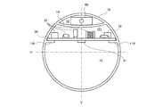
カバー部材1の内周面には、図4に示すように、一対の載置台部11が、カバー部材1の管軸に沿った垂直横断面Vを挟んで対向するように管軸方向(X方向)に延設されている。一対の載置台部11は、カバー部材1の管軸に沿った水平横断面Hよりも上側において、水平横断面Hと平行に形成されている。
また、カバー部材1の内周面には、一対の取付レール部12が垂直横断面Vを挟んで対向するように管軸方向(X方向)に延設されている。一対の取付レール部12は、水平横断面H及び一対の載置台部11よりも上側であるカバー部材1の内周面の頂部近傍において、垂直横断面V側に向かって取付爪121を突出させるように形成されている。
エンド部材2は、図1及び図2に示すように、カバー部材1の管軸方向(X方向)の両端においてカバー部材1を覆うように取り付けられて固定されている。エンド部材2には一対の端子21が設けられている。端子21は、照明装置100を取り付ける照明器具のソケットの端子(図示省略)を介して電力が供給されるように構成されている。また、端子21は、接続ケーブル(図示省略)を介して、電源基板5に接続されている。
LED実装基板3a,3bは、図2及び3に示すように、LED実装基板3a,3bの長手方向(X方向)に沿って直列に連結されており、それぞれ複数のLED31が所定の間隔をおいて設けられている。LED実装基板3a,3bは、コネクタ32を介して互いに電気的に接続されており、コネクタ32は、LED実装基板3a,3bに実装されたLED31から放射される光を妨げないように、LED実装基板3a,3bの裏面(LED31が実装された面の裏側の面)に配置されている。なお、以下においては、連結したLED実装基板3a,3bを1つのLED実装基板3として表すことがある。
本実施形態においては基板自体を高い放熱性を有するものとしており、LED実装基板3a,3bは、例えば高熱伝導性ガラスコンポジット材のような放熱性を有する材質で形成されている。
また、本実施形態においては、LED実装基板3a,3bに実装されるLED31として従来のものよりも高効率化されたものを用いている。従来のLEDが、例えば駆動電流65mAという条件下で光束出力が25lmとなる特性を有しているのに対して、本実施形態で用いるLED31は、例えば駆動電流65mAという条件下で光束出力が37.5lmとなる特性を有している。このようなLED31であれば低電流量駆動でも十分な照度で発光するため、発熱量そのものが少なくてすむ。つまり、LED31を40mAで駆動すれば、37.5×40/65=約23lmとなり、従来のLEDと同等の明るさを確保できる。
このようにLED実装基板3a,3bを高い放熱性を有するものとし、またLED31を低電流で駆動することにより、放熱のためにヒートシンクのような別の部材をLED実装基板3a,3bに取り付ける必要がなくなる。
LED実装基板3は、その両側端部がカバー部材1の一対の載置台部11にそれぞれ載置されるように、カバー部材1に対してスライド挿入して装着される。一対の載置台部11は水平横断面Hよりも上側に形成されているため、挿入されたLED実装基板3は、その両側端部がそれぞれ載置台部11とその上側の内周面との間に挟まるようにして安定的に保持される。このような構造とすることにより、LED実装基板3を保持するための部材を別途用意することなく、LED実装基板3を安定的にカバー部材1内に収納することができる。また、LED実装基板3は着脱自在に挿入されているだけであり、エンド部材2を取り外すことにより、必要に応じて容易に交換可能な構造となっている。
シャフト4は、金属製の長尺部材である。原材料として用いられる金属は、例えば熱膨張係数が10~28(×10-6/℃)の範囲にある金属(アルミニウム、マグネシウム、ステンレス鋼、等)であれば好適に用いることができ、特に熱膨張係数が10~12(×10-6/℃)の範囲にあるステンレス鋼を用いることが好ましい。このようにシャフト4を金属製とすることにより、LED31の発熱によりカバー部材1が熱膨張したときにもシャフト4が熱膨張することはほとんどなく、照明装置100が大きく変形してしまうことを防ぐことができる。なお、シャフト4の製造方法も原材料として用いられる金属の特性に応じて適宜選択することができる。
シャフト4には、軽量化を図るために、その軸心に沿って貫通孔41がその全長に亘って設けられており、照明装置100全体の軽量化に寄与している。この貫通孔41はエンド部材2とのビス止めにも用いられる。また、シャフト4の両側面部には、カバー部材1の一対の取付レール部12が嵌合するように、その全長に亘って取付溝部42が設けられている。シャフト4の上面(カバー部材1の内周面側の面)及び底面(上面の裏側の面)は、いずれもRがつけられてやや丸みを帯びた形状を有しており、また断面視で上下対称の形状となっている。
シャフト4は、取付溝部42を取付レール部12に嵌合させるように、カバー部材1に対してスライド挿入して装着される。挿入されたシャフト4は、上記のようにエンド部材2とビス止めされていることのみならず、カバー部材1の内周面と同じRを持つように形成されていることによって、カバー部材1の内周面との隙間がなく一対の取付レール部12の間に挟持されることになり、安定的に保持される。また、シャフト4は上下対称の形状となっていることにより、取付ミスが生じることもない。
電源基板5は、外部から供給される交流の電力をLED31の駆動用の直流の電力に変換するように構成されている。電源基板5は、LED実装基板3aの長手方向(X方向)の外側に配置されており、接続ケーブル(図示省略)を介して、端子21及び制御基板6に接続されている。また、電源基板5は、エンド部材2で覆われた部分のカバー部材1の内側に配置されている。これにより、電源基板5を外部から見えにくくすることが可能である。
制御基板6は、無線による調光やオンオフを行うときにLED31の点灯を制御するように構成されている。制御基板6は、LED実装基板3bの長手方向(X方向)の外側に配置されており、接続ケーブル(図示省略)を介して、LED実装基板3b及び電源基板5に接続されている。また、制御基板6は、エンド部材2で覆われた部分のカバー部材1の内側に配置されている。これにより、制御基板6を外部から見えにくくすることが可能である。無線による調光やオンオフの機能を持たない廉価版モデルにおいては制御基板6が不要となるので、その場合は電源基板5を二つに分け、空いたスペースにそのうちの一つを配置してもよい。これにより、電源基板5を覆うエンド部材2を小型化することが可能になる。
以上説明したような本実施形態に係る照明装置100では、LED実装基板3a,3bの裏面がカバー部材1内の空洞13に向かって開放されていることにより、LED実装基板3a,3bのLED実装面のみならず裏面にも配線パターンを設けることができるため、電源から各配線までの沿面距離を十分に確保することができる。また、LED実装基板3a,3b基板を連結するためのコネクタ32をLED実装基板3a,3b基板の裏面に配置することができるため、LEDから放射される光がコネクタ32に遮光されることもなくなる。また、シャフト4をカバー部材1内に配置することにより、LEDの発熱によりカバー部材1が熱膨張したときに照明装置100が大きく変形してしまうことを防ぐこともできる。このような構成の照明装置100であれば、安全規格を満たしやすく、遮光による発光ムラが生じにくい。
(第1変形例)
続いて、上述した実施形態の第1変形例について図5を参照しながら説明する。本変形例は上述した実施形態のカバー部材及びシャフトの形状が異なるだけであり、カバー部材及びシャフト以外の共通する構成についての説明は省略する。
続いて、上述した実施形態の第1変形例について図5を参照しながら説明する。本変形例は上述した実施形態のカバー部材及びシャフトの形状が異なるだけであり、カバー部材及びシャフト以外の共通する構成についての説明は省略する。
図5に示すように、本変形例のカバー部材1Aは、上述のカバー部材1における一対の取付レール部12の代わりに、水平横断面H及び一対の載置台部11よりも上側であるカバー部材1Aの内周面の頂部近傍において隔壁14を有している。隔壁14は管軸方向(X方向)に延設されており、隔壁14によってLED実装基板3が収納されている空間15と隔てられた空間16がカバー部材1の内部に形成される。
シャフト4Aは断面視略矩形の長尺柱状部材であり、軽量化を図るために、その軸心に沿って貫通孔41Aがその全長に亘って設けられている。シャフト4Aは空間16に挿設される。
本変形例においても、LED実装基板3の裏面がカバー部材1A内の空洞(図5におけるLED実装基板3上側の空間151)に向かって開放されており、上述のカバー部材1の実施形態と同様の効果が実現される。
(第2変形例)
続いて、上述した第1変形例を応用した第2変形例を、図6を参照しながら説明する。なお、上述した実施形態及び第1変形例と共通する構成についての説明は省略する。
続いて、上述した第1変形例を応用した第2変形例を、図6を参照しながら説明する。なお、上述した実施形態及び第1変形例と共通する構成についての説明は省略する。
図6に示すように、本変形例の基板3Bは、裏面に発光素子31を駆動するための電源回路が実装されている。本変形例においては、カバー部材1Bの内周面に延設される一対の載置台部11Bの位置を下げ、水平横断面Hに近い位置に配置している。これにより基板3Bと隔壁14との間の空間151が拡がり、電源回路の実装部品33が収まる領域が確保される。
このように基板3Bの裏面に電源回路が実装されていても、シャフト4Bと基板3Bとの間には隔壁14があるため、シャフト4Bが導電性を有していても沿面距離が問題になることがない。また、基板3Bの裏面に電源回路を実装することにより、本変形例の照明装置には電源基板5が不要となるので、エンド部材2を小型化することができ、ひいては照明装置全体を小型化することができる。
以上説明した実施形態は、本発明の理解を容易にするために記載されたものであって、本発明を限定するために記載されたものではない。したがって、上記実施形態に開示された各要素は、本発明の技術的範囲に属する全ての設計変更や均等物をも含む趣旨である。
例えば、本実施形態においては、2つのLED実装基板3a,3bを連結しているが、これに限られるものではなく、照明装置100の寸法や用途等に応じて、LED実装基板が1つだけであってもよいし、3つ以上のLED実装基板を連結してもよい。
また、カバー部材1,1Aは、必ずしも全体が透過性又は拡散性を有する樹脂製である必要はなく、照明装置100が、求められる用途や機能に応じて、LED31から放射される光を照射可能である限りは、複数の部材を組み合わせた構造を有していてもよい。例えば、LED31から光が放射される方向だけを透過性及び/又は拡散性を有する樹脂で形成し、LED31の光が照射される側と反対側は、内部が見えないように着色された不透明の樹脂や樹脂以外の素材により形成されていてもよい。
100 照明装置
1,1A,1B カバー部材
11 載置台部
12 取付レール部
121 取付爪
13 空洞
14 隔壁
15,151,16 空間
2 エンド部材
21 端子
3,3a,3b LED実装基板(基板)
31 LED(発光素子)
32 コネクタ
4,4A シャフト(長尺部材)
41,41A 貫通孔
42 取付溝部
1,1A,1B カバー部材
11 載置台部
12 取付レール部
121 取付爪
13 空洞
14 隔壁
15,151,16 空間
2 エンド部材
21 端子
3,3a,3b LED実装基板(基板)
31 LED(発光素子)
32 コネクタ
4,4A シャフト(長尺部材)
41,41A 貫通孔
42 取付溝部
Claims (5)
- 表面に発光素子が実装された基板と、
該基板を内部に収納し、前記発光素子から放射される光を透過及び/又は拡散する直管形状のカバー部材と、
該カバー部材内に配置された金属製の長尺部材とを備え、
前記基板の裏面が前記カバー部材内の空洞に向かって開放されていることを特徴とする照明装置。 - 前記カバー部材の内周面には一対の載置台部が対向するように管軸方向に延設されており、
前記基板の両側端部が前記一対の載置台部にそれぞれ載置されていることを特徴とする、請求項1に記載の照明装置。 - 前記カバー部材の内周面には一対の取付レール部が対向するように管軸方向に延設されており、
前記長尺部材が前記一対の取付レール部の間に挟持されていることを特徴とする、請求項1又は2に記載の照明装置。 - 前記長尺部材が、前記基板が収納されている空間と隔壁によって隔てられた前記カバー部材内の空間に挿設されていることを特徴とする、請求項1又は2に記載の照明装置。
- 前記基板の裏面に前記発光素子を駆動するための電源回路が実装されていることを特徴とする、請求項4に記載の照明装置。
Applications Claiming Priority (2)
| Application Number | Priority Date | Filing Date | Title |
|---|---|---|---|
| JP2016-256584 | 2016-12-28 | ||
| JP2016256584 | 2016-12-28 |
Publications (1)
| Publication Number | Publication Date |
|---|---|
| WO2018124154A1 true WO2018124154A1 (ja) | 2018-07-05 |
Family
ID=62709410
Family Applications (1)
| Application Number | Title | Priority Date | Filing Date |
|---|---|---|---|
| PCT/JP2017/046833 Ceased WO2018124154A1 (ja) | 2016-12-28 | 2017-12-27 | 照明装置 |
Country Status (1)
| Country | Link |
|---|---|
| WO (1) | WO2018124154A1 (ja) |
Citations (3)
| Publication number | Priority date | Publication date | Assignee | Title |
|---|---|---|---|---|
| JP2011049075A (ja) * | 2009-08-27 | 2011-03-10 | Daiichi-Tsusho Co Ltd | 照明装置および光源装置 |
| JP2014029816A (ja) * | 2012-07-31 | 2014-02-13 | Kyouwa Device:Kk | Ledランプ。 |
| JP2015015110A (ja) * | 2013-07-03 | 2015-01-22 | 東芝ライテック株式会社 | 発光モジュール及び照明装置 |
-
2017
- 2017-12-27 WO PCT/JP2017/046833 patent/WO2018124154A1/ja not_active Ceased
Patent Citations (3)
| Publication number | Priority date | Publication date | Assignee | Title |
|---|---|---|---|---|
| JP2011049075A (ja) * | 2009-08-27 | 2011-03-10 | Daiichi-Tsusho Co Ltd | 照明装置および光源装置 |
| JP2014029816A (ja) * | 2012-07-31 | 2014-02-13 | Kyouwa Device:Kk | Ledランプ。 |
| JP2015015110A (ja) * | 2013-07-03 | 2015-01-22 | 東芝ライテック株式会社 | 発光モジュール及び照明装置 |
Similar Documents
| Publication | Publication Date | Title |
|---|---|---|
| KR101348739B1 (ko) | 엘이디조명장치 및 그를 가지는 엘이디조명시스템 | |
| JPWO2011122518A1 (ja) | 管状ランプおよび照明器具 | |
| TW201502425A (zh) | Led燈條式燈座及具有該燈座之燈泡 | |
| US20160025276A1 (en) | Light emitting diode spotlight | |
| JP5946008B2 (ja) | 照明器具 | |
| JP2015069846A (ja) | 発光モジュール、管形発光ランプおよび照明器具 | |
| JP6297299B2 (ja) | 照明器具 | |
| JP5294044B2 (ja) | 照明器具 | |
| JP2012238502A (ja) | 発光装置、照明装置および照明器具 | |
| JP2012054018A (ja) | 発光素子ランプおよび照明器具 | |
| KR101061218B1 (ko) | Led조명장치용 방열판 | |
| JP6548153B2 (ja) | 照明装置 | |
| JP2011210729A (ja) | 蛍光灯形ledランプ及び照明装置 | |
| KR200455629Y1 (ko) | Led 램프 | |
| KR20160011579A (ko) | 발광 다이오드 전구 | |
| WO2018124154A1 (ja) | 照明装置 | |
| JP5888624B2 (ja) | 照明器具 | |
| TW201400746A (zh) | Led燈管 | |
| JP2012049079A (ja) | 照明器具 | |
| CN206608831U (zh) | 一种侧面发光光纤led氛围灯节点光源 | |
| JP6436382B2 (ja) | 照明装置 | |
| JP2013201041A (ja) | 発光モジュール、照明装置および照明器具 | |
| TWM470201U (zh) | 照明裝置 | |
| KR101371117B1 (ko) | 엘이디 조명 장치 | |
| RU129191U1 (ru) | Бескорпусная светодиодная лампа |
Legal Events
| Date | Code | Title | Description |
|---|---|---|---|
| 121 | Ep: the epo has been informed by wipo that ep was designated in this application |
Ref document number: 17889146 Country of ref document: EP Kind code of ref document: A1 |
|
| NENP | Non-entry into the national phase |
Ref country code: DE |
|
| 122 | Ep: pct application non-entry in european phase |
Ref document number: 17889146 Country of ref document: EP Kind code of ref document: A1 |
|
| NENP | Non-entry into the national phase |
Ref country code: JP |