WO2018116716A1 - 半導体装置、半導体装置の製造方法、及び、電子機器 - Google Patents
半導体装置、半導体装置の製造方法、及び、電子機器 Download PDFInfo
- Publication number
- WO2018116716A1 WO2018116716A1 PCT/JP2017/041518 JP2017041518W WO2018116716A1 WO 2018116716 A1 WO2018116716 A1 WO 2018116716A1 JP 2017041518 W JP2017041518 W JP 2017041518W WO 2018116716 A1 WO2018116716 A1 WO 2018116716A1
- Authority
- WO
- WIPO (PCT)
- Prior art keywords
- box layer
- layer
- semiconductor device
- substrate
- soi
- Prior art date
- Legal status (The legal status is an assumption and is not a legal conclusion. Google has not performed a legal analysis and makes no representation as to the accuracy of the status listed.)
- Ceased
Links
Images









Classifications
-
- H—ELECTRICITY
- H10—SEMICONDUCTOR DEVICES; ELECTRIC SOLID-STATE DEVICES NOT OTHERWISE PROVIDED FOR
- H10D—INORGANIC ELECTRIC SEMICONDUCTOR DEVICES
- H10D30/00—Field-effect transistors [FET]
- H10D30/60—Insulated-gate field-effect transistors [IGFET]
- H10D30/791—Arrangements for exerting mechanical stress on the crystal lattice of the channel regions
- H10D30/796—Arrangements for exerting mechanical stress on the crystal lattice of the channel regions having memorised stress for introducing strain in the channel regions, e.g. recrystallised polysilicon gates
-
- H—ELECTRICITY
- H10—SEMICONDUCTOR DEVICES; ELECTRIC SOLID-STATE DEVICES NOT OTHERWISE PROVIDED FOR
- H10D—INORGANIC ELECTRIC SEMICONDUCTOR DEVICES
- H10D30/00—Field-effect transistors [FET]
- H10D30/60—Insulated-gate field-effect transistors [IGFET]
- H10D30/791—Arrangements for exerting mechanical stress on the crystal lattice of the channel regions
- H10D30/798—Arrangements for exerting mechanical stress on the crystal lattice of the channel regions being provided in or under the channel regions
-
- H—ELECTRICITY
- H10—SEMICONDUCTOR DEVICES; ELECTRIC SOLID-STATE DEVICES NOT OTHERWISE PROVIDED FOR
- H10D—INORGANIC ELECTRIC SEMICONDUCTOR DEVICES
- H10D30/00—Field-effect transistors [FET]
- H10D30/01—Manufacture or treatment
- H10D30/021—Manufacture or treatment of FETs having insulated gates [IGFET]
- H10D30/031—Manufacture or treatment of FETs having insulated gates [IGFET] of thin-film transistors [TFT]
- H10D30/0321—Manufacture or treatment of FETs having insulated gates [IGFET] of thin-film transistors [TFT] comprising silicon, e.g. amorphous silicon or polysilicon
- H10D30/0323—Manufacture or treatment of FETs having insulated gates [IGFET] of thin-film transistors [TFT] comprising silicon, e.g. amorphous silicon or polysilicon comprising monocrystalline silicon
-
- H—ELECTRICITY
- H10—SEMICONDUCTOR DEVICES; ELECTRIC SOLID-STATE DEVICES NOT OTHERWISE PROVIDED FOR
- H10D—INORGANIC ELECTRIC SEMICONDUCTOR DEVICES
- H10D30/00—Field-effect transistors [FET]
- H10D30/60—Insulated-gate field-effect transistors [IGFET]
- H10D30/67—Thin-film transistors [TFT]
- H10D30/674—Thin-film transistors [TFT] characterised by the active materials
- H10D30/6741—Group IV materials, e.g. germanium or silicon carbide
- H10D30/6743—Silicon
-
- H—ELECTRICITY
- H10—SEMICONDUCTOR DEVICES; ELECTRIC SOLID-STATE DEVICES NOT OTHERWISE PROVIDED FOR
- H10D—INORGANIC ELECTRIC SEMICONDUCTOR DEVICES
- H10D86/00—Integrated devices formed in or on insulating or conducting substrates, e.g. formed in silicon-on-insulator [SOI] substrates or on stainless steel or glass substrates
- H10D86/01—Manufacture or treatment
-
- H—ELECTRICITY
- H10—SEMICONDUCTOR DEVICES; ELECTRIC SOLID-STATE DEVICES NOT OTHERWISE PROVIDED FOR
- H10D—INORGANIC ELECTRIC SEMICONDUCTOR DEVICES
- H10D86/00—Integrated devices formed in or on insulating or conducting substrates, e.g. formed in silicon-on-insulator [SOI] substrates or on stainless steel or glass substrates
- H10D86/201—Integrated devices formed in or on insulating or conducting substrates, e.g. formed in silicon-on-insulator [SOI] substrates or on stainless steel or glass substrates the substrates comprising an insulating layer on a semiconductor body, e.g. SOI
-
- H—ELECTRICITY
- H10—SEMICONDUCTOR DEVICES; ELECTRIC SOLID-STATE DEVICES NOT OTHERWISE PROVIDED FOR
- H10P—GENERIC PROCESSES OR APPARATUS FOR THE MANUFACTURE OR TREATMENT OF DEVICES COVERED BY CLASS H10
- H10P90/00—Preparation of wafers not covered by a single main group of this subclass, e.g. wafer reinforcement
- H10P90/19—Preparing inhomogeneous wafers
- H10P90/1904—Preparing vertically inhomogeneous wafers
- H10P90/1906—Preparing SOI wafers
-
- H—ELECTRICITY
- H10—SEMICONDUCTOR DEVICES; ELECTRIC SOLID-STATE DEVICES NOT OTHERWISE PROVIDED FOR
- H10W—GENERIC PACKAGES, INTERCONNECTIONS, CONNECTORS OR OTHER CONSTRUCTIONAL DETAILS OF DEVICES COVERED BY CLASS H10
- H10W10/00—Isolation regions in semiconductor bodies between components of integrated devices
- H10W10/01—Manufacture or treatment
- H10W10/011—Manufacture or treatment of isolation regions comprising dielectric materials
- H10W10/014—Manufacture or treatment of isolation regions comprising dielectric materials using trench refilling with dielectric materials, e.g. shallow trench isolations
-
- H—ELECTRICITY
- H10—SEMICONDUCTOR DEVICES; ELECTRIC SOLID-STATE DEVICES NOT OTHERWISE PROVIDED FOR
- H10W—GENERIC PACKAGES, INTERCONNECTIONS, CONNECTORS OR OTHER CONSTRUCTIONAL DETAILS OF DEVICES COVERED BY CLASS H10
- H10W10/00—Isolation regions in semiconductor bodies between components of integrated devices
- H10W10/01—Manufacture or treatment
- H10W10/061—Manufacture or treatment using SOI processes together with lateral isolation, e.g. combinations of SOI and shallow trench isolations
-
- H—ELECTRICITY
- H10—SEMICONDUCTOR DEVICES; ELECTRIC SOLID-STATE DEVICES NOT OTHERWISE PROVIDED FOR
- H10W—GENERIC PACKAGES, INTERCONNECTIONS, CONNECTORS OR OTHER CONSTRUCTIONAL DETAILS OF DEVICES COVERED BY CLASS H10
- H10W10/00—Isolation regions in semiconductor bodies between components of integrated devices
- H10W10/10—Isolation regions comprising dielectric materials
- H10W10/17—Isolation regions comprising dielectric materials formed using trench refilling with dielectric materials, e.g. shallow trench isolations
-
- H—ELECTRICITY
- H10—SEMICONDUCTOR DEVICES; ELECTRIC SOLID-STATE DEVICES NOT OTHERWISE PROVIDED FOR
- H10W—GENERIC PACKAGES, INTERCONNECTIONS, CONNECTORS OR OTHER CONSTRUCTIONAL DETAILS OF DEVICES COVERED BY CLASS H10
- H10W10/00—Isolation regions in semiconductor bodies between components of integrated devices
- H10W10/10—Isolation regions comprising dielectric materials
- H10W10/181—Semiconductor-on-insulator [SOI] isolation regions, e.g. buried oxide regions of SOI wafers
Definitions
- the present disclosure relates to a semiconductor device, a semiconductor device manufacturing method, and an electronic apparatus.
- Patent Document 1 Japanese Unexamined Patent Application Publication No. 2011-199112 (Patent Document 1) describes that a stress liner film that generates strain in a channel region is provided on a transistor having the channel region.
- Non-Patent Document 1 a SiN film having a film stress is deposited on an SOI layer and subjected to high-temperature annealing to cause deformation of the BOX layer due to creep, and stress is applied to the SOI layer even after the SiN film is removed.
- the method of leaving the deformation due to creep in the BOX layer of the SOI substrate has an advantage that stress can be applied to the entire channel region.
- development of a structure and method that can further increase the degree of deformation remaining in the BOX layer is required.
- an object of the present disclosure is to provide a semiconductor device and a method for manufacturing the semiconductor device that can further increase the degree of deformation remaining in the BOX layer, and further provide an electronic apparatus including the semiconductor device.
- a semiconductor device includes: A semiconductor device formed using an SOI substrate comprising a substrate, a BOX layer formed on the substrate, and an SOI layer formed on the BOX layer, In at least a part of the BOX layer disposed in the inactive area adjacent to the active area, a part or all of the BOX layer is removed, The portion of the BOX layer where the SOI layer that forms the active region is arranged is configured so that deformation for applying stress to the SOI layer remains. It is a semiconductor device.
- a method for manufacturing a semiconductor device according to the first aspect of the present disclosure for achieving the above object is as follows.
- a method for manufacturing a semiconductor device formed using an SOI substrate comprising a substrate, a BOX layer formed on the substrate, and an SOI layer formed on the BOX layer, Forming a stress film on the SOI layer;
- the stress film and the SOI layer located in the inactive area adjacent to the active area are removed, Thereafter, for at least a part of the BOX layer arranged in the inactive area adjacent to the active area, a part or all of the BOX layer is removed,
- the entire SOI substrate is subjected to high-temperature annealing so that creep occurs in the BOX layer due to the stress of the stress film, and then the stress film is removed.
- a step of leaving deformation due to creep in the BOX layer A method for manufacturing a semiconductor device.
- the electronic device for achieving the above-described object is: An electronic apparatus comprising a semiconductor device formed using an SOI substrate comprising a substrate, a BOX layer formed on the substrate, and an SOI layer formed on the BOX layer, In at least a part of the BOX layer disposed in the inactive area adjacent to the active area, a part or all of the BOX layer is removed, The portion of the BOX layer where the SOI layer that forms the active region is arranged is configured so that deformation for applying stress to the SOI layer remains. It is an electronic device.
- a part or all of the BOX layer is removed in at least a part of the BOX layer disposed in the inactive region adjacent to the active region. According to this structure, the portion of the BOX layer where the SOI layer that forms the active region is easily deformed to apply stress to the SOI layer, so that the carrier mobility can be further improved. it can.
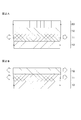
- FIG. 1A to FIG. 1C are schematic diagrams for explaining deformation that occurs in a high-temperature annealing process when a stress film having a compressive stress is formed.
- FIG. 2A and FIG. 2B are schematic diagrams for explaining deformation caused by high-temperature annealing when a stress film having a compressive stress is formed following FIG. 1C.
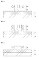
- FIG. 3A to FIG. 3C are schematic diagrams for explaining the deformation caused by the high-temperature annealing process in the configuration in which the mesa structure is stopped at the SOI layer.
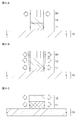
- FIG. 4A to FIG. 4C are schematic diagrams for explaining the deformation caused by the high-temperature annealing process in the configuration in which the mesa structure is extended to the BOX layer.
- FIG. 1A to FIG. 1C are schematic diagrams for explaining deformation that occurs in a high-temperature annealing process when a stress film having a compressive stress is formed.
- FIG. 2A and FIG. 2B are schematic diagram
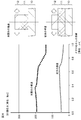
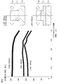
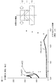
- FIG. 5 is a graph of stress simulation for explaining the difference in stress of the SOI layer due to the difference in mesa structure.
- FIG. 6 is a graph of stress simulation for explaining the relationship between the time during which high-temperature annealing is performed and the stress of the SOI layer.
- FIG. 7 is a graph of stress simulation for explaining the relationship between the temperature at which high-temperature annealing is performed and the stress of the SOI layer.
- FIG. 8 is a graph corresponding to FIG. 5 and is a graph of stress simulation for explaining the difference in stress of the SOI layer due to the difference in mesa structure when the SOI layer is made thicker. .
- FIG. 9 is a graph of stress simulation for explaining the relationship between the film thickness of the BOX layer, the removal amount of the BOX layer, and the stress of the SOI layer. It is a graph of stress simulation for demonstrating the difference of the stress of an SOI layer resulting from the difference of a mesa structure.
- 10A to 10C are schematic cross-sectional views for explaining the method for manufacturing the semiconductor device according to the first embodiment.
- 11A and 11B are schematic cross-sectional views for explaining the method for manufacturing the semiconductor device, following FIG. 10C.
- 12A and 12B are schematic cross-sectional views for explaining the method for manufacturing the semiconductor device, following FIG. 11B.
- 13A to 13C are schematic cross-sectional views for explaining the method for manufacturing the semiconductor device, following FIG. 12B.
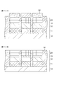
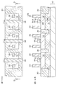
- FIG. 14A is a schematic plan view for explaining the structure of a semiconductor device having a structure in which the mesa structure is fixed to the SOI layer.
- 14B is a cross-sectional view taken along the line AA in FIG. 14A.
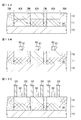
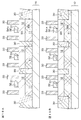
- FIG. 15A is a schematic plan view for explaining the structure of a semiconductor device having a configuration in which a BOX layer is removed from a part of an inactive region.
- FIG. 15B is a cross-sectional view taken along the line BB of FIG. 15A.
- FIG. 16A is a schematic plan view for explaining the structure of a semiconductor device having a configuration in which all of the BOX layers are removed from all of the inactive regions. 16B is a cross-sectional view taken along the line CC of FIG. 16A.
- FIG. 17 is a graph of stress simulation for explaining the relationship between the stress of the SOI layer and the area of the mesa structure.
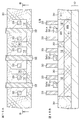
- FIG. 18A is a schematic plan view for explaining the structure of a semiconductor device having a configuration in which the BOX layer is partially removed in all of the inactive regions.
- 18B is a cross-sectional view taken along the line DD of FIG. 18A.
- 19A and 19B are schematic cross-sectional views for explaining the structure of a semiconductor device in which a configuration in which all of the BOX layer is removed and a configuration in which the BOX layer is partially removed are mixed.
- 19A corresponds to FIG. 16B
- FIG. 19B corresponds to FIG. 18B.
- 20A is a schematic plan view for explaining the structure of a semiconductor device having a configuration in which all of the BOX layer is removed in all of the inactive regions and the upper portion of the substrate is partially removed.
- 20B is a cross-sectional view taken along line EE of FIG. 20A.
- 21A and 21B are schematic cross-sectional views for explaining the structure of a semiconductor device in which a configuration in which all of the BOX layer is removed and a part of the upper portion of the substrate is removed and another configuration are mixed.
- 21A corresponds to FIG. 20B
- FIG. 21B corresponds to FIG. 16B.
- the BOX layer located in the active region can be configured to include a plurality of regions having different thicknesses.
- a part of the substrate may be removed on at least a part of the substrate surface located in the region where all of the BOX layer is removed.
- the BOX layer and the substrate located in the inactive region can each include a plurality of regions having different thicknesses.
- stress can be applied to the SOI layer in the active region forming the nMOS transistor so that the crystal lattice is expanded.
- stress can be applied to the SOI layer in the active region forming the pMOS transistor so that the crystal lattice is narrowed.
- the semiconductor device is: an active region for forming an nMOS type transistor and an active region for forming a pMOS type transistor;
- the BOX layer located in the inactive region adjacent to the active region forming the nMOS type transistor and the BOX layer located in the inactive region adjacent to the active region forming the pMOS type transistor have different thicknesses. It can be set as the structure comprised in this way.
- a part of the substrate is removed on at least a part of the substrate surface located in the region where all of the BOX layer is removed,
- the thickness of the substrate located in the inactive region adjacent to the active region forming the nMOS type transistor is different from the thickness of the substrate located in the inactive region adjacent to the active region forming the pMOS type transistor. It can be set as the structure comprised.
- the difference between the thickness of the BOX layer located in the active region and the thickness of the BOX layer located in the inactive region adjacent to the active region is 50 nanometers or more It can be.
- the BOX layer disposed in the inactive area adjacent to the active area may be configured such that all of the BOX layer is removed.
- the BOX layer in the portion where the SOI layer forming the active region is disposed is configured so that deformation due to creep generated by high-temperature annealing applied to the SOI substrate remains. It can be set as the mode currently performed.
- the semiconductor device of the present disclosure including the various preferable configurations described above can be configured such that stress exceeding 100 MPa is applied to the SOI layer on the BOX layer in the active region at room temperature.
- the thickness of the SOI layer in the active region may be 200 nanometers or less.
- the thickness of the SOI layer in the active region may be 200 nanometers or less.
- an element isolation insulating layer may be provided in the inactive region so as to cover the entire surface including the BOX layer.
- the method for manufacturing a semiconductor device includes: A method for manufacturing a semiconductor device formed using an SOI substrate comprising a substrate, a BOX layer formed on the substrate, and an SOI layer formed on the BOX layer, Forming a stress film on the SOI layer; Next, the stress film and the SOI layer located in the inactive area adjacent to the active area are removed, Thereafter, for at least a part of the BOX layer arranged in the inactive area adjacent to the active area, a part or all of the BOX layer is removed, Next, the entire SOI substrate is subjected to high-temperature annealing so that creep occurs in the BOX layer due to the stress of the stress film, and then the stress film is removed. A step of leaving deformation due to creep in the BOX layer.
- it may be configured to further include a step of removing a part of the substrate on at least a part of the substrate surface located in the region where the entire BOX layer is removed.
- a stress film having a compressive stress is formed on an SOI layer in an active region where an nMOS transistor is formed, and an active transistor in which a pMOS transistor is formed.
- a stress film having a tensile stress can be formed on the SOI layer in the region.
- the electronic device is An electronic apparatus comprising a semiconductor device formed using an SOI substrate comprising a substrate, a BOX layer formed on the substrate, and an SOI layer formed on the BOX layer, In at least a part of the BOX layer disposed in the inactive area adjacent to the active area, a part or all of the BOX layer is removed, The portion of the BOX layer where the SOI layer forming the active region is arranged is configured so that deformation for applying stress to the SOI layer remains.
- the electronic device can be configured to be a display, an image sensor, a memory, an RF switch, a power amplifier, or a low noise amplifier.
- an SOI substrate such as an SOI wafer used in the present disclosure is not particularly limited as long as it does not hinder the implementation of the present disclosure.
- the SOI substrate can be constituted by a method in which an oxide film is formed on at least one of a support substrate and an active substrate, these are bonded together under heat treatment, and then the active substrate is polished to a predetermined thickness.
- the material constituting the stress film is not particularly limited as long as a predetermined stress is maintained during the high temperature annealing treatment. More specifically, any material that has stress and has higher rigidity than the SOI layer or the BOX layer may be used.
- the material constituting the stress film is silicon nitride (SiN x ).
- the film made of silicon nitride can be formed by a known method such as a CVD method.
- the direction and magnitude of the stress of the film can be controlled by the type of film formation method, the atmosphere during film formation, exposure by energy rays, the setting of the hydrogen density in the film, and the like.
- a film having compressive stress can be formed using PECVD (Plasma Enhanced Chemical Vapor Deposition), and a film having tensile stress can be formed using LPCVD (Low Pressure Chemical Vapor Deposition). Stress values in various films and layers can be measured by strain measurement by Raman spectroscopy or NBD (Nano Beam Diffraction) method using TEM.
- the viewpoint of causing deformation due to creep basically, it is preferable to perform high-temperature annealing at a temperature of about half or more of the absolute temperature of the melting point of the material constituting the BOX layer. Specifically, it is preferable to carry out at 1100 ° C or higher, more preferably 1200 ° C or higher.
- the degree of deformation due to creep increases as the processing time for performing the high temperature annealing process increases, and increases as the temperature for performing the high temperature annealing process increases.
- the first embodiment relates to a semiconductor device, a method for manufacturing a semiconductor device, and an electronic apparatus according to a first aspect of the present disclosure.
- FIG. 1A to FIG. 1C are schematic diagrams for explaining deformation that occurs in a high-temperature annealing process when a stress film having a compressive stress is formed.
- FIG. 2A and FIG. 2B are schematic diagrams for explaining deformation caused by high-temperature annealing when a stress film having a compressive stress is formed following FIG. 1C.
- FIG. 1A shows a cross section of the SOI substrate 1.
- the SOI substrate 1 includes a substrate 10 made of, for example, silicon, a BOX layer 11 formed on the substrate 10, and an SOI layer 12 formed on the BOX layer 11.
- FIG. 1B shows a state in which a stress film is formed on the SOI layer.
- the stress film 20 is made of, for example, silicon nitride.
- the stress film 20 is formed to have a compressive stress.
- the stress film 20 having a compressive stress exhibits the property of spreading toward the outside. Therefore, a force in the direction of spreading outward acts on the SOI layer 12 below the stress film 20.
- FIG. 1C schematically shows deformation when a high-temperature annealing treatment is performed on an SOI substrate on which a stress film is formed.
- An annealing process is performed on the SOI substrate 1 on which the stress film 20 is formed, for example, at a temperature of 1200 ° C. for 2 minutes.
- a temperature of 1200 ° C. for 2 minutes Generally, in a high temperature environment exceeding half the absolute value of the melting point of the material, deformation due to creep tends to occur. Since the melting point of silicon oxide forming the BOX layer 11 is about 1800 ° C., the BOX layer 11 is deformed by creep while being pulled by the SOI layer 12.
- FIG. 2A schematically shows an SOI substrate that has been returned to room temperature after high-temperature annealing.
- FIG. 2B shows a state where the stress film is further removed.
- the stress film 20 has been described as having compressive stress.
- the stress film 20 has a tensile stress
- the BOX layer 11 is deformed in a direction narrowing inward.
- a force acts on the SOI layer 12 on the BOX layer 11 in the direction of narrowing inward, in other words, the direction of narrowing the crystal lattice of the SOI layer 12.
- FIG. 3A to FIG. 3C are schematic diagrams for explaining the deformation caused by the high-temperature annealing process in the configuration in which the mesa structure is stopped at the SOI layer.
- FIG. 3A shows a state where a mesa structure is formed by patterning the stress film and the SOI layer using the SOI substrate on which the stress film is formed.
- the substrate 10 and the BOX layer 11 are not patterned.
- the stress film 20 is described as having a compressive stress, but the present invention is not limited to this. The same applies to FIG. 4 described later.
- FIG. 3B schematically shows deformation when the high-temperature annealing treatment is performed on the mesa structure shown in FIG. 3A. Then, the state which removed the stress film
- the BOX layer 11 is in a state of being restrained by the substrate 10 having higher rigidity. Therefore, even if the BOX layer 11 is softened by the high temperature annealing treatment, the degree of deformation is suppressed by the influence of the substrate 10 (see FIG. 3B).
- the mesa structure is applied to the BOX layer in order to further promote the deformation of the BOX layer by the high-temperature annealing treatment.
- FIG. 4A to FIG. 4C are schematic diagrams for explaining the deformation caused by the high-temperature annealing process in the configuration in which the mesa structure is extended to the BOX layer.
- FIG. 4A shows a state where a mesa structure is formed by patterning the stress film, the SOI layer, and the BOX layer using the SOI substrate on which the stress film is formed.
- the substrate 10 is not patterned.
- the stress film 20 is described as having a compressive stress, but the present invention is not limited to this.
- FIG. 4B schematically shows deformation when the high-temperature annealing treatment is performed on the mesa structure shown in FIG. 4A. Then, the state which removed the stress film
- the BOX layer 11 is subdivided. Therefore, in the BOX layer 11 having the mesa structure, the degree of restraint of the substrate 10 is relaxed and the volume covered by the stress film 20 is also reduced. Thereby, the deformation of the BOX layer 11 by the high-temperature annealing process is further promoted (see FIG. 4B).
- the BOX layer 11 in the portion where the SOI layer 12 forming the active region is disposed is configured such that deformation due to creep generated by the high-temperature annealing process applied to the SOI substrate 1 remains, and Since the deformation of the BOX layer 11 by the high-temperature annealing treatment is further promoted, the action of force on the SOI layer 12 becomes larger, and the force acts on the SOI layer 12 in the direction of expanding the crystal lattice. (See FIG. 4C).
- FIG. 5 shows the stress of the SOI layer for the configuration in which the mesa structure is stopped in the SOI layer (sometimes referred to as a conventional structure) and the configuration in which the mesa structure is extended to the BOX layer (structure of the present disclosure). The graph which compared is shown.
- the SOI substrate 1 has the same specifications.
- the SOI layer 12 has a thickness of 30 nanometers
- the BOX layer 11 has a thickness of 400 nanometers
- the mesa structure has a rectangular shape with a side length of 2 micrometers.
- the conditions for the high-temperature annealing treatment are such that the temperature is 1200 ° C. and 10 minutes.
- the stress of the SOI layer 12 is a stress in a state where the stress film 20 is removed after the high temperature annealing treatment.
- the horizontal axis of the graph is the distance from the center of the mesa structure, and the vertical axis of the graph is the stress of the SOI layer 12. The same applies to other graphs described later.
- the stress of the SOI layer 12 is three times or more that of the conventional structure. Therefore, stress exceeding 100 MPa can be applied to the SOI layer 12 on the BOX layer 11 in the active region at room temperature, and the mobility of electrons in the SOI layer 12 is further improved. If an nMOS type transistor is configured, the effect of reducing the drain-source on-resistance R on excluding the wiring resistance and contact resistance of the contact is expected to be three times or more that of the conventional structure.
- a force acts on the SOI layer 12 in the direction of narrowing the crystal lattice. Therefore, if a pMOS transistor is to be formed, the stress film 20 having a tensile stress may be formed and the same process as described above may be performed. Thus, stress can be applied to the SOI layer 12 in the active region forming the pMOS transistor so that the crystal lattice is narrowed.
- the processing time for performing the high temperature annealing process is longer.
- FIG. 6 the relationship between the processing time for performing the high-temperature annealing and the stress of the SOI layer 12 will be described.
- FIG. 6 is a graph showing the stress of the SOI layer when the time for high-temperature annealing at a temperature of 1200 ° C. is 10 minutes, 5 minutes, and 2 minutes in the structure of the present disclosure described above.
- the SOI layer has a thickness of 30 nanometers
- the BOX layer 11 has a thickness of 400 nanometers
- the mesa structure has a rectangular shape with a side length of 2 micrometers.
- the horizontal axis of the graph is the distance from the center of the mesa structure, and the vertical axis of the graph is the stress of the SOI layer 12.
- the stress of the SOI layer 12 increases as the time for performing the high-temperature annealing treatment increases.
- the temperature when the high temperature annealing is performed is higher.
- FIG. 7 the relationship between the temperature at which the high temperature annealing process is performed and the stress of the SOI layer 12 will be described.
- FIG. 7 is a graph showing the stress of the SOI layer when the above-described structure of the present disclosure is subjected to a high-temperature annealing process at a temperature of 1300 ° C. for 2 minutes and a high-temperature annealing process at a temperature of 1200 ° C. for 2 minutes. It is.
- the SOI layer 12 has a thickness of 30 nanometers
- the BOX layer 11 has a thickness of 400 nanometers
- the mesa structure has a rectangular shape with a side length of 2 micrometers.
- the horizontal axis of the graph is the distance from the center of the mesa structure, and the vertical axis of the graph is the stress of the SOI layer.
- the stress of the SOI layer 12 increases as the temperature at which the high-temperature annealing treatment is performed increases.
- the stress is dispersed as the SOI layer 12 becomes thicker. Therefore, qualitatively, it is desirable that the SOI layer 12 is somewhat thin.
- FIG. 8 is a graph corresponding to FIG. 5 and is a graph for explaining a difference in stress of the SOI layer due to a difference in mesa structure when the SOI layer is made thicker.
- the thickness of the SOI layer 12 is 150 nanometers
- the thickness of the BOX layer 11 is 400 nanometers
- the mesa structure has a rectangular shape with a side length of 2 micrometers.
- the conditions for the high temperature annealing treatment are a temperature of 1200 ° C. and 2 minutes.
- the stress of the SOI layer 12 is three times or more that of the conventional structure. However, in contrast to FIG. 5, the stress of the SOI layer 12 is slightly reduced. From the viewpoint of securing a certain amount of stress in the SOI layer 12, the thickness of the SOI layer 12 in the active region is preferably 200 nanometers or less.
- the BOX layer 11 preferably has a thickness of 100 nanometers or more.
- FIG. 9 is a graph for explaining the relationship between the thickness of the BOX layer, the removal amount of the BOX layer, and the stress of the SOI layer.
- FIG. 9 shows a structure in which the BOX layer 11 has a thickness of 400 nm and a mesa structure in which the BOX layer 11 is completely removed (represented as [400/400 nm]), and the BOX layer 11 has a thickness of 1000 nm and a mesa structure.
- a configuration in which all the layers 11 are removed represented as [1000/1000 nm]
- a thickness of the BOX layer 11 of 1000 nanometers a mesa structure in which the BOX layer 11 is removed by 400 nanometers (represented as [400/1000 nm])
- the stress of the SOI layer 12 when the high temperature annealing process at a temperature of 1200 ° C. is performed for 10 minutes is shown.
- the stress is higher in the case where the thickness of the BOX layer 11 is 1000 nanometers than in the case where the thickness of the BOX layer 11 is 400 nanometers in the case where the BOX layer 11 is completely removed. This indicates that as the BOX layer 11 is thicker, the influence of restraint of the substrate 10 is reduced and the deformation of the high-temperature annealing process is promoted.
- the configuration of [400/1000 nm] in which the thickness of the BOX layer 11 is 1000 nm and 400 nm is removed is the configuration in which the BOX layer 11 is completely removed with the thickness of the BOX layer 11 being [400/400 nm] [400/400 nm].
- the stress is greater than. This is presumably because the BOX layer 11 remains under the etched region, and the influence of the restraint of the substrate 10 is mitigated.
- the difference is preferably 50 nanometers or more.
- the semiconductor device having the above structure can be used for various electronic devices.
- the present invention can be applied to a display, an image sensor, a memory, an RF switch, a power amplifier, a low noise amplifier, or the like.
- the semiconductor device according to the first embodiment shown in FIG. A semiconductor device formed using an SOI substrate 1 comprising a substrate 10, a BOX layer 11 formed on the substrate 10, and an SOI layer 12 formed on the BOX layer 11, In at least a part of the BOX layer 11 arranged in the inactive area adjacent to the active area, a part or all of the BOX layer 11 is removed, The portion of the BOX layer 11 where the SOI layer 12 that forms the active region is disposed is configured such that deformation for applying stress to the SOI layer 12 remains.
- the manufacturing method of the semiconductor device according to the first embodiment is as follows: A method for manufacturing a semiconductor device formed using an SOI substrate 1 comprising a substrate 10, a BOX layer 11 formed on the substrate 10, and an SOI layer 12 formed on the BOX layer 11, Forming a stress film 20 on the SOI layer 12; Next, the stress film 20 and the SOI layer 12 located in the inactive region adjacent to the active region are removed, Thereafter, a part or all of the BOX layer 11 is removed from at least a part of the BOX layer 11 arranged in the inactive region adjacent to the active region, Next, the entire SOI substrate 1 is subjected to a high-temperature annealing treatment so that creep occurs in the BOX layer 11 due to the stress of the stress film 20, and then the stress film 20 is removed. This includes a step of leaving deformation due to creep in the BOX layer 11.
- 10 to 13 are schematic cross-sectional views for explaining the method for manufacturing the semiconductor device according to the first embodiment.
- Step-100 (see FIGS. 10A to 10C) An SOI substrate 1 including a substrate 10, a BOX layer 11 formed on the substrate 10, and an SOI layer 12 formed on the BOX layer 11 is prepared (see FIG. 10A), and the SOI substrate 1 is thermally oxidized. An oxide film 13 is formed on the surface of the SOI layer 12 (see FIG. 10B). Next, a stress film 20 is formed by depositing on the oxide film 13 silicon nitride that serves as a mask during element isolation etching and an etching stopper during planarization (see FIG. 10C).
- the stress film 20 having a stress in the compressive direction is formed, and when forming a pMOS transistor, the stress film 20 having a stress in the tensile direction may be formed.
- the stress and the direction of the stress film 20 can be adjusted by the type of film formation method, the atmosphere during film formation, exposure by energy rays, the setting of the hydrogen density in the film, and the like.
- Step-110 (see FIGS. 11A and 11B)
- the stress film 20, the oxide film 13, and the SOI layer 12 are etched to cut off a portion that becomes a mesa structure.
- etching is performed on an inactive area (represented by reference numeral INA) around an active area (represented by reference numeral ACA).
- the etching may be dry etching or wet etching.
- the stress film 20 is patterned by a known method so as to correspond to the active area ACA (see FIG. 11A).
- the SOI layer 12, the oxide film 13, and the BOX layer 11 are etched to form a mesa structure (see FIG. 11B).
- the etching is performed without leaving the BOX layer 11 in the inactive area INA.
- the present invention is not limited to this.
- the thickness of the stress film 20 is preferably set so as to remain at 50 nanometers or more when the mesa structure is formed.
- Step-120 high-temperature annealing is performed. What is necessary is just to set suitably the temperature and time which perform a high temperature annealing process suitably according to the specification of a semiconductor device. Basically, it is preferable to perform the treatment at 1100 ° C. or more for 1 minute or more.
- the deformation caused by the high-temperature annealing process is the same as that described with reference to FIGS. 4A to 4C, and thus the description thereof is omitted.
- the element isolation insulating layer 30 is formed using, for example, the HDP method (High Density Plasma) (see FIG. 12A).
- planarization is performed. For example, a process such as etching is performed using the stress film 20 as a stopper (see FIG. 12B). Thereafter, planarization is performed using, for example, CMP (Chemical Mechanical Polishing), the stress film 20 and the oxide film 13 are removed, and the SOI layer 12 in the active region is exposed (see FIG. 13A). [Step-140] (see FIGS. 13B and 13C) Thereafter, a transistor is formed in the SOI layer 12 in the active region. For example, steps such as impurity implantation, formation of the gate insulating film 31 and the gate electrode 32 (see FIG. 13B), and formation of the source / drain electrode 33 (FIG. 13C) may be appropriately performed. For the convenience of illustration, the illustration of the planarizing film and the openings provided therein is omitted.
- a step of removing a part of the substrate 10 may be further included in at least a part of the substrate surface located in the region where the entire BOX layer 11 is removed.
- a stress film 20 having compressive stress is formed on the SOI layer 12 in the active region where the nMOS type transistor is formed, and the active region where the pMOS type transistor is formed.
- a stress film 20 having a tensile stress may be formed on the SOI layer 12.
- the stress film 20 can be formed where necessary by a known patterning method.
- nMOS type and pMOS type are mixed and, for example, it is desired to make an electrical difference between them, for example, a configuration in which one of them is not a mesa structure is also conceivable.
- a configuration in which one of them is not a mesa structure is also conceivable.
- the etching of the BOX layer 11 is not necessarily perpendicular to the active region.
- it may have a shape that enters the lower side of the SOI layer 12 or a shape that spreads outward.
- FIG. 14A is a schematic plan view for explaining the structure of a semiconductor device having a structure in which the mesa structure is stopped in the SOI layer.
- 14B is a cross-sectional view taken along the line AA in FIG. 14A.
- the thickness of the BOX layer 11 is uniform in the wafer surface as shown in FIG.
- the film thickness of the BOX layer 11 is not uniform in the wafer surface.
- FIG. 15A is a schematic plan view for explaining the structure of a semiconductor device in which the BOX layer is removed from a part of the inactive region.
- FIG. 15B is a cross-sectional view taken along the line BB of FIG. 15A.
- the element isolation insulating layer 30 is provided so as to cover the entire surface including the BOX layer 11 in the non-active region including other drawings described later.
- FIG. 15 shows an example of a structure in which all of the BOX layer is removed around the group of three active regions, and the BOX layer is left as it is between the active regions.
- the BOX layer located in the non-active region includes a plurality of regions having different thicknesses.
- FIG. 16 shows an example of a structure in which all the BOX layers are removed around the group of three active regions, and all the BOX layers are also removed between the active regions. As shown in these drawings, in the structure of the present disclosure, a part of the BOX layer 11 is replaced with the element isolation insulating layer 30.
- FIG. 17 is a schematic graph for explaining the relationship between the stress of the SOI layer and the area of the mesa structure.
- the SOI layer 12 has a thickness of 30 nanometers
- the BOX layer 11 has a thickness of 400 nanometers
- the mesa structure has a rectangular shape with a side length of 2 micrometers, a rectangular side with a side length of 4 micrometers, The rectangular shape has one side of 30 micrometers and the other side of 160 micrometers.
- the stress value remaining in the SOI layer 12 tends to increase as the area of the mesa structure is smaller, more specifically, as the channel length in the channel region is narrower. This is because the deformation of the BOX layer 11 due to creep is promoted as the area of the mesa structure is smaller. Therefore, the width in the channel length direction in the active region is preferably 30 micrometers or less.
- the BOX layer 11 arranged in the inactive region adjacent to the active region is configured such that all of the BOX layer 11 is removed, in other words, the BOX layer so as to subdivide the active region.
- the structure of FIG. 16 which etches 11 is preferable.
- the present invention when the present invention is applied to a multi-gate type transistor having a long overall W length, the effect can be more remarkably achieved by etching the BOX layer beside each source / drain.
- FIG. 18A is a schematic plan view for explaining the structure of a semiconductor device having a configuration in which the BOX layer is partially removed in all of the inactive regions.
- 18B is a cross-sectional view taken along the line DD of FIG. 18A.
- the structure shown in FIG. 18 is such that the thickness of the BOX layer is different between the active region and the inactive region.
- the BOX layer 11 located in the inactive region may include a plurality of regions having different thicknesses.
- a configuration in which the BOX layer 11 is entirely removed at a certain specific portion in the wafer and the BOX layer 11 is partially removed at other specific portions may be mixed.
- 19A and 19B are schematic cross-sectional views for explaining the structure of a semiconductor device in which a configuration in which all of the BOX layer 11 is removed and a configuration in which the BOX layer 11 is partially removed are mixed.
- 19A corresponds to FIG. 16B
- FIG. 19B corresponds to FIG. 18B.
- the BOX layer 11 located in the inactive region adjacent to the active region forming the pMOS transistor can be a semiconductor device configured to have a different thickness.
- FIG. 20A is a schematic plan view for explaining the structure of a semiconductor device having a structure in which all of the BOX layer 11 is removed in all of the inactive regions and a part of the upper portion of the substrate is removed.
- 20B is a cross-sectional view taken along line EE of FIG. 20A. In this configuration, a part of the substrate is removed on at least a part of the substrate surface located in the region where all of the BOX layer 11 is removed.
- the BOX layer 11 may be completely removed at a specific portion in the wafer, and the upper portion of the substrate 10 below the BOX layer 11 may be partially removed at other specific portions.
- 21A and 21B are schematic cross-sectional views for explaining the structure of a semiconductor device in which a configuration in which all of the BOX layer 11 is removed and a part of the upper portion of the substrate 10 is removed and another configuration are mixed. .
- FIG. 21A corresponds to FIG. 19B
- FIG. 21B corresponds to FIG. 16B.
- the BOX layer 11 and the substrate 10 located in the inactive area may include a plurality of areas having different thicknesses. For example, at least a part of the surface of the substrate 10 located in a region where all of the BOX layer 11 is removed, a part of the substrate 10 is removed, and a non-adjacent region adjacent to the active region forming the nMOS transistor is formed.
- the thickness of the substrate 10 located in the active region and the thickness of the substrate 10 located in the inactive region adjacent to the active region where the pMOS transistor is formed can be a semiconductor device configured differently. .
- a semiconductor device formed using an SOI substrate comprising a substrate, a BOX layer formed on the substrate, and an SOI layer formed on the BOX layer, In at least a part of the BOX layer disposed in the inactive area adjacent to the active area, a part or all of the BOX layer is removed, The portion of the BOX layer where the SOI layer that forms the active region is arranged is configured so that deformation for applying stress to the SOI layer remains.
- Semiconductor device. [A2]
- the BOX layer located in the non-active region includes a plurality of regions having different thicknesses. The semiconductor device according to [A1].
- a part of the substrate is removed on at least a part of the substrate surface located in the region where all of the BOX layer is removed;
- Each of the BOX layer and the substrate located in the inactive region includes a plurality of regions having different thicknesses.
- [A6] Stress is applied to the SOI layer in the active region forming the pMOS type transistor so that the crystal lattice is narrowed.
- a part of the substrate is removed on at least a part of the substrate surface located in the region where all of the BOX layer is removed,
- the thickness of the substrate located in the inactive region adjacent to the active region forming the nMOS type transistor is different from the thickness of the substrate located in the inactive region adjacent to the active region forming the pMOS type transistor. It is configured,
- [A9] The difference between the thickness of the BOX layer located in the active region and the thickness of the BOX layer located in the non-active region adjacent to the active region is 50 nanometers or more.
- [A14] The width in the channel length direction in the active region is 30 micrometers or less.
- a method for manufacturing a semiconductor device formed using an SOI substrate comprising a substrate, a BOX layer formed on the substrate, and an SOI layer formed on the BOX layer, Forming a stress film on the SOI layer; Next, the stress film and the SOI layer located in the inactive area adjacent to the active area are removed, Thereafter, for at least a part of the BOX layer arranged in the inactive area adjacent to the active area, a part or all of the BOX layer is removed, Next, the entire SOI substrate is subjected to high-temperature annealing so that creep occurs in the BOX layer due to the stress of the stress film, and then the stress film is removed. A step of leaving deformation due to creep in the BOX layer, A method for manufacturing a semiconductor device.
- [B2] A step of removing a part of the substrate in at least a part of the substrate surface located in the region where the entire BOX layer is removed; The manufacturing method of the semiconductor device as described in said [B1].
- [B3] a stress film having compressive stress is formed on an SOI layer in an active region for forming an nMOS transistor, and a stress film having tensile stress is formed on an SOI layer in an active region for forming a pMOS transistor; The manufacturing method of the semiconductor device as described in said [B1] or [B2].
- An electronic apparatus comprising a semiconductor device formed using an SOI substrate comprising a substrate, a BOX layer formed on the substrate, and an SOI layer formed on the BOX layer, In at least a part of the BOX layer disposed in the inactive area adjacent to the active area, a part or all of the BOX layer is removed, The portion of the BOX layer where the SOI layer that forms the active region is arranged is configured so that deformation for applying stress to the SOI layer remains.
- the electronic device is a display, an image sensor, a memory, an RF switch, a power amplifier, or a low noise amplifier. The electronic device according to [C1] above.
- SYMBOLS 1 ... SOI substrate, 10 ... Substrate, 11 ... BOX layer, 12 ... SOI layer, 13 ... Oxide film, 20 ... Stress film, 30 ... Element isolation insulating layer, 31 ... Gate insulating film, 32 ... Gate electrode, 33 ... Source / drain electrode, ACA ... Active region, INA ... Inactive region
Landscapes
- Thin Film Transistor (AREA)
- Metal-Oxide And Bipolar Metal-Oxide Semiconductor Integrated Circuits (AREA)
- Element Separation (AREA)
Abstract
基板と、基板上に形成されたBOX層と、BOX層上に形成されたSOI層とから成るSOI基板を用いて形成された半導体装置であって、アクティブ領域に隣接する非アクティブ領域に配置されたBOX層のうち少なくとも一部において、BOX層の一部あるいは全てが除去されており、アクティブ領域を形成するSOI層が配置される部分のBOX層は、SOI層に応力を加えるための変形が残留するように構成されている。
Description
本開示は、半導体装置、半導体装置の製造方法、及び、電子機器に関する。
半導体装置における電気的特性の向上を目的として、チャネル領域に応力を加えることによってキャリア移動度を向上させるといったことが提案されている。チャネル領域に応力を加える方法として、チャネル領域を形成する材料とは格子定数が異なる材料を用いて下地層を形成した後にその上にチャネル領域を形成するといった方法や、ゲート電極上やソースドレイン領域上に応力を有する膜(応力膜)を形成するといった方法が提案されている。例えば、特開2011-199112号公報(特許文献1)には、チャネル領域を有するトランジスタ上に、チャネル領域に歪みを発生させるストレスライナー膜を設けるといったことが記載されている。
また、SOI(Silicon on Insulator)基板を用いた半導体装置において、クリープ(Creep)現象による変形をBOX層(Buried Oxide層)に残留させることで、BOX層上のTop Si層(SOI層)に応力を加えるといった方法が提案されている(例えば、非特許文献1参照)。これは、膜応力をもつSiN膜をSOI層上に堆積し、高温アニールを施すことでBOX層にクリープによる変形を生じさせ、SiN膜の除去後においてもSOI層に応力を加えるといった方法である。
A.Bonnevialle et al.,"A New Method to Induce Local Tensile Strain in SOI Wafers: First Strain Results of the "BOXCreep" Technique",Extended Abstracts of the 2015 International Conference on Solid State Devices and Materials, Sapporo, 2015,pp1110-1111, STMicroelectronics
SOI基板のBOX層にクリープによる変形を残留させる方法は、チャネル領域全般に応力を加えることができるといった利点を備えている。しかしながら、キャリア移動度の更なる向上のために、BOX層に残留させる変形の程度をより大きくすることができる構造や方法の開発が求められている。
従って、本開示の目的は、BOX層に残留させる変形の程度をより大きくすることができる半導体装置や半導体装置の製造方法、更には、係る半導体装置を備えた電子機器を提供することにある。
上記の目的を達成するための本開示の第1の態様に係る半導体装置は、
基板と、基板上に形成されたBOX層と、BOX層上に形成されたSOI層とから成るSOI基板を用いて形成された半導体装置であって、
アクティブ領域に隣接する非アクティブ領域に配置されたBOX層のうち少なくとも一部において、BOX層の一部あるいは全てが除去されており、
アクティブ領域を形成するSOI層が配置される部分のBOX層は、SOI層に応力を加えるための変形が残留するように構成されている、
半導体装置である。
基板と、基板上に形成されたBOX層と、BOX層上に形成されたSOI層とから成るSOI基板を用いて形成された半導体装置であって、
アクティブ領域に隣接する非アクティブ領域に配置されたBOX層のうち少なくとも一部において、BOX層の一部あるいは全てが除去されており、
アクティブ領域を形成するSOI層が配置される部分のBOX層は、SOI層に応力を加えるための変形が残留するように構成されている、
半導体装置である。
上記の目的を達成するための本開示の第1の態様に係る半導体装置の製造方法は、
基板と、基板上に形成されたBOX層と、BOX層上に形成されたSOI層とから成るSOI基板を用いて形成される半導体装置の製造方法であって、
SOI層上に応力膜を形成し、
次いで、アクティブ領域に隣接する非アクティブ領域に位置する応力膜とSOI層を除去し、
その後、アクティブ領域に隣接する非アクティブ領域に配置されたBOX層のうち少なくとも一部について、BOX層の一部あるいは全てを除去し、
次いで、応力膜の応力によってBOX層にクリープが生ずるようにSOI基板全体に高温アニール処理を施した後、応力膜を除去する、
ことによってBOX層にクリープによる変形を残留させる工程を含む、
半導体装置の製造方法である。
基板と、基板上に形成されたBOX層と、BOX層上に形成されたSOI層とから成るSOI基板を用いて形成される半導体装置の製造方法であって、
SOI層上に応力膜を形成し、
次いで、アクティブ領域に隣接する非アクティブ領域に位置する応力膜とSOI層を除去し、
その後、アクティブ領域に隣接する非アクティブ領域に配置されたBOX層のうち少なくとも一部について、BOX層の一部あるいは全てを除去し、
次いで、応力膜の応力によってBOX層にクリープが生ずるようにSOI基板全体に高温アニール処理を施した後、応力膜を除去する、
ことによってBOX層にクリープによる変形を残留させる工程を含む、
半導体装置の製造方法である。
上記の目的を達成するための本開示の第1の態様に係る電子機器は、
基板と、基板上に形成されたBOX層と、BOX層上に形成されたSOI層とから成るSOI基板を用いて形成された半導体装置を備えた電子機器であって、
アクティブ領域に隣接する非アクティブ領域に配置されたBOX層のうち少なくとも一部において、BOX層の一部あるいは全てが除去されており、
アクティブ領域を形成するSOI層が配置される部分のBOX層は、SOI層に応力を加えるための変形が残留するように構成されている、
電子機器である。
基板と、基板上に形成されたBOX層と、BOX層上に形成されたSOI層とから成るSOI基板を用いて形成された半導体装置を備えた電子機器であって、
アクティブ領域に隣接する非アクティブ領域に配置されたBOX層のうち少なくとも一部において、BOX層の一部あるいは全てが除去されており、
アクティブ領域を形成するSOI層が配置される部分のBOX層は、SOI層に応力を加えるための変形が残留するように構成されている、
電子機器である。
本開示の半導体装置にあっては、アクティブ領域に隣接する非アクティブ領域に配置されたBOX層のうち少なくとも一部において、BOX層の一部あるいは全てが除去されている。この構造によれば、アクティブ領域を形成するSOI層が配置される部分のBOX層は、SOI層に応力を加えるための変形が残留しやすくなるので、キャリア移動度の更なる向上を図ることができる。
以下、図面を参照して、実施形態に基づいて本開示を説明する。本開示は実施形態に限定されるものではなく、実施形態における種々の数値や材料は例示である。以下の説明において、同一要素または同一機能を有する要素には同一符号を用いることとし、重複する説明は省略する。尚、説明は、以下の順序で行う。
1.本開示に係る、半導体装置、半導体装置の製造方法、及び、電子機器、全般に関する説明
2.第1の実施形態
3.その他
1.本開示に係る、半導体装置、半導体装置の製造方法、及び、電子機器、全般に関する説明
2.第1の実施形態
3.その他
[本開示に係る、半導体装置、半導体装置の製造方法、及び、電子機器、全般に関する説明]
本開示に係る半導体装置や係る半導体装置を用いた電子機器、及び、本開示の半導体装置の製造方法によって製造される半導体装置(以下、これらを単に、本開示と呼ぶ場合がある)において、非アクティブ領域に位置するBOX層は、厚さが異なる複数の領域を含んでいる構成とすることができる。
本開示に係る半導体装置や係る半導体装置を用いた電子機器、及び、本開示の半導体装置の製造方法によって製造される半導体装置(以下、これらを単に、本開示と呼ぶ場合がある)において、非アクティブ領域に位置するBOX層は、厚さが異なる複数の領域を含んでいる構成とすることができる。
上述した好ましい構成を含む本開示において、BOX層の全てが除去されてなる領域に位置する基板面のうち少なくとも一部において、基板の一部が除去されている構成とすることができる。この場合において、非アクティブ領域に位置するBOX層および基板は、それぞれ、厚さが異なる複数の領域を含んでいる構成とすることができる。
上述した各種の好ましい構成を含む本開示において、nMOS型のトランジスタを形成するアクティブ領域のSOI層には、結晶格子が広げられるように応力が加えられる構成とすることができる。また、pMOS型のトランジスタを形成するアクティブ領域のSOI層には、結晶格子が狭められるように応力が加えられる構成とすることができる。
上述した各種の好ましい構成を含む本開示において、半導体装置は、
nMOS型のトランジスタを形成するアクティブ領域とpMOS型のトランジスタを形成するアクティブ領域とを備えており、
nMOS型のトランジスタを形成するアクティブ領域に隣接する非アクティブ領域に位置するBOX層と、pMOS型のトランジスタを形成するアクティブ領域に隣接する非アクティブ領域に位置するBOX層とは、それぞれ厚さが異なるように構成されている構成とすることができる。
nMOS型のトランジスタを形成するアクティブ領域とpMOS型のトランジスタを形成するアクティブ領域とを備えており、
nMOS型のトランジスタを形成するアクティブ領域に隣接する非アクティブ領域に位置するBOX層と、pMOS型のトランジスタを形成するアクティブ領域に隣接する非アクティブ領域に位置するBOX層とは、それぞれ厚さが異なるように構成されている構成とすることができる。
この場合において、
BOX層の全てが除去されてなる領域に位置する基板面のうち少なくとも一部において、基板の一部が除去されており、
nMOS型のトランジスタを形成するアクティブ領域に隣接する非アクティブ領域に位置する基板の厚さと、pMOS型のトランジスタを形成するアクティブ領域に隣接する非アクティブ領域に位置する基板の厚さとは、異なるように構成されている構成とすることができる。
BOX層の全てが除去されてなる領域に位置する基板面のうち少なくとも一部において、基板の一部が除去されており、
nMOS型のトランジスタを形成するアクティブ領域に隣接する非アクティブ領域に位置する基板の厚さと、pMOS型のトランジスタを形成するアクティブ領域に隣接する非アクティブ領域に位置する基板の厚さとは、異なるように構成されている構成とすることができる。
上述した各種の好ましい構成を含む本開示において、アクティブ領域に位置するBOX層の厚さと、アクティブ領域に隣接する非アクティブ領域に位置するBOX層の厚さとの差は、50ナノメートル以上である構成とすることができる。あるいは又、アクティブ領域に隣接する非アクティブ領域に配置されたBOX層は、その全てが除去されている構成とすることができる。
上述した各種の好ましい構成を含む本開示において、アクティブ領域を形成するSOI層が配置される部分のBOX層は、SOI基板に施された高温アニール処理で生じたクリープによる変形が残留するように構成されている態様とすることができる。
上述した各種の好ましい構成を含む本開示の半導体装置は、アクティブ領域におけるBOX層上のSOI層には、常温において100MPaを超える応力が加えられる構成とすることができる。
上述した各種の好ましい構成を含む本開示において、アクティブ領域におけるSOI層の厚さは200ナノメートル以下である構成とすることができる。
上述した各種の好ましい構成を含む本開示において、アクティブ領域におけるSOI層の厚さは200ナノメートル以下である構成とすることができる。
上述した各種の好ましい構成を含む本開示において、非アクティブ領域には、BOX層を含む全面を覆うように素子分離絶縁層が設けられている構成とすることができる。
上述したように、本開示に係る半導体装置の製造方法は、
基板と、基板上に形成されたBOX層と、BOX層上に形成されたSOI層とから成るSOI基板を用いて形成される半導体装置の製造方法であって、
SOI層上に応力膜を形成し、
次いで、アクティブ領域に隣接する非アクティブ領域に位置する応力膜とSOI層を除去し、
その後、アクティブ領域に隣接する非アクティブ領域に配置されたBOX層のうち少なくとも一部について、BOX層の一部あるいは全てを除去し、
次いで、応力膜の応力によってBOX層にクリープが生ずるようにSOI基板全体に高温アニール処理を施した後、応力膜を除去する、
ことによってBOX層にクリープによる変形を残留させる工程を含む。
基板と、基板上に形成されたBOX層と、BOX層上に形成されたSOI層とから成るSOI基板を用いて形成される半導体装置の製造方法であって、
SOI層上に応力膜を形成し、
次いで、アクティブ領域に隣接する非アクティブ領域に位置する応力膜とSOI層を除去し、
その後、アクティブ領域に隣接する非アクティブ領域に配置されたBOX層のうち少なくとも一部について、BOX層の一部あるいは全てを除去し、
次いで、応力膜の応力によってBOX層にクリープが生ずるようにSOI基板全体に高温アニール処理を施した後、応力膜を除去する、
ことによってBOX層にクリープによる変形を残留させる工程を含む。
この場合において、BOX層の全てが除去されてなる領域に位置する基板面のうち少なくとも一部において、基板の一部を除去する工程を更に含む構成とすることができる。
上述した好ましい構成を含む本開示に係る半導体装置の製造方法において、nMOS型のトランジスタを形成するアクティブ領域のSOI層上には圧縮応力を有する応力膜を形成し、pMOS型のトランジスタを形成するアクティブ領域のSOI層上には引張応力を有する応力膜を形成する構成とすることができる。
上述したように、本開示に係る電子機器は、
基板と、基板上に形成されたBOX層と、BOX層上に形成されたSOI層とから成るSOI基板を用いて形成された半導体装置を備えた電子機器であって、
アクティブ領域に隣接する非アクティブ領域に配置されたBOX層のうち少なくとも一部において、BOX層の一部あるいは全てが除去されており、
アクティブ領域を形成するSOI層が配置される部分のBOX層は、SOI層に応力を加えるための変形が残留するように構成されている。
基板と、基板上に形成されたBOX層と、BOX層上に形成されたSOI層とから成るSOI基板を用いて形成された半導体装置を備えた電子機器であって、
アクティブ領域に隣接する非アクティブ領域に配置されたBOX層のうち少なくとも一部において、BOX層の一部あるいは全てが除去されており、
アクティブ領域を形成するSOI層が配置される部分のBOX層は、SOI層に応力を加えるための変形が残留するように構成されている。
この場合において、上記電子機器は、ディスプレイ、イメージセンサ、メモリ、RFスイッチ、パワーアンプ、または、ローノイズアンプである構成とすることができる。
本開示に用いられるSOIウエハーなどのSOI基板の構成は、本開示の実施に支障がない限り、特に限定するものではない。例えば、SOI基板は、支持基板と活性基板との少なくとも一方に酸化膜を形成した後、これらを熱処理下で貼り合わせ、その後、活性基板を所定厚まで研磨するといった方法で構成することができる。
応力膜を構成する材料は、高温アニール処理時において所定の応力が保持される限りは、特に限定するものではない。より具体的には、応力を有し、且つ、SOI層やBOX層よりも剛性が大きい材料であればよい。
応力膜を構成する材料として、例えば、窒化シリコン(SiNX)を挙げることができる。窒化シリコンから成る膜は、例えばCVD法などの周知の方法によって成膜することができる。膜の応力の向きやその大きさは、成膜法の種類や、成膜時の雰囲気、エネルギー線による曝露、膜中の水素密度の設定などによって制御することができる。例えば、PECVD(Plasma Enhanced Chemical Vapor Deposition)を用いて圧縮応力を持つ膜を形成することができるし、LPCVD(Low Pressure Chemical Vapor Deposition)を用いて引張応力を持つ膜を形成することができる。各種の膜や層における応力値は、ラマン分光法やTEMを用いたNBD(Nano Beam Diffraction)法によるひずみ測定によって測定することができる。
クリープによる変形を起こさせるといった観点から、基本的には、BOX層を構成する材料における融点の絶対温度に対して約半分程度以上の温度で高温アニール処理を行なうことが好ましい。具体的には、1100°C以上、より好ましくは、1200°C以上で行なうことが好ましい。定性的には、クリープによる変形の程度は、高温アニール処理を行なう処理時間が長いほど大きくなり、また、高温アニール処理を行なう温度が高いほど大きくなる。
本明細書における各種の条件は、厳密に成立する場合の他、実質的に成立する場合にも満たされる。設計上あるいは製造上生ずる種々のばらつきの存在は許容される。また、以下の説明で用いる各図面は模式的なものであり、実際の寸法やその割合を示すものではない。
[第1の実施形態]
第1の実施形態は、本開示の第1の態様に係る、半導体装置、半導体装置の製造方法、及び、電子機器に関する。
第1の実施形態は、本開示の第1の態様に係る、半導体装置、半導体装置の製造方法、及び、電子機器に関する。
本開示の理解を助けるため、先ず、SOI層上に応力膜を形成した状態で高温アニール処理を施したときの変形について説明する。
図1Aないし図1Cは、圧縮応力を有する応力膜を形成した場合に、高温アニール処理で生ずる変形を説明するための模式図である。図2A及び図2Bは、図1Cに引き続き、圧縮応力を有する応力膜を形成した場合に、高温アニール処理で生ずる変形を説明するための模式図である。
図1Aは、SOI基板1の断面を示す。SOI基板1は、たとえばシリコンから成る基板10、基板10上に形成されたBOX層11、BOX層11上に形成されたSOI層12から成る。
図1Bは、SOI層上に応力膜を形成した状態を示す。応力膜20は、例えば、窒化シリコンから構成されている。ここでは、nMOS型用として、応力膜20は圧縮応力を有するように形成されているとして説明する。圧縮応力を有する応力膜20は、外側に向かって広がろうとする性質を示す。このため、応力膜20下のSOI層12には、外側に広げる方向の力が作用する。
図1Cは、応力膜が形成されたSOI基板に高温アニール処理を施すときの変形を模式的に示す。
基本的には、降伏加重よりも小さい力が物体に作用しても物体に変形は残留しない。しかしながら、力が作用している状態で物体を高温環境下に晒しておくと、時間の経過とともに物体に変形が生じ残留する現象、即ち、所謂クリープ現象が起こる。
応力膜20が形成されたSOI基板1について、例えば、1200°C下で2分といった条件でアニール処理を行なう。一般的に、材料の融点の絶対値の半分を超える高温環境下であると、クリープによる変形が起こりやすくなる。BOX層11を形成する酸化シリコンの融点は約1800°Cであるので、BOX層11には、SOI層12に引っ張られる形でクリープによる変形が生ずる。
図2Aは、高温アニール処理後に常温に戻された状態のSOI基板を模式的に示す。図2Bは、更に、応力膜を除去した状態を示す。
常温に戻った状態において、BOX層11にはクリープによる変形がある程度残留する。通常、応力膜20を除去すれば、SOI層12への応力も緩和される。しかしながら、BOX層11にはクリープによる変形が残留している。従って、BOX層11上のSOI層12には、外側に向かって広がろうとする方向、換言すれば、SOI層12の結晶格子を広げる方向に力が作用する。
上述の例では、応力膜20は圧縮応力を有するとして説明した。応力膜20が引張応力を有する場合、BOX層11には、内側に狭まる方向の変形が生ずる。結果として、BOX層11上のSOI層12には、内側に向かって狭まろうとする方向、換言すれば、SOI層12の結晶格子を狭める方向に力が作用する。
次いで、非引用文献1に開示された、メサ構造をSOI層に止めた構成における高温アニール処理について説明する。
図3Aないし図3Cは、メサ構造をSOI層に止めた構成において、高温アニール処理で生ずる変形を説明するための模式図である。
図3Aは、応力膜が形成されたSOI基板を用いて、応力膜、SOI層をパターニングしてメサ構造を形成した状態を示す。基板10とBOX層11とはパターニングされていない。尚、説明の都合上、応力膜20は圧縮応力を有するとして説明するが、これに限るものではない。後述する図4についても同様である。
図3Aに示すメサ構造に高温アニール処理を施すときの変形を、図3Bに模式的に示す。その後、常温に戻された状態で、応力膜を除去した状態を、図3Cに示す。
BOX層11は、より剛性の高い基板10に拘束された状態である。従って、高温アニール処理によってBOX層11が軟化したとしても、基板10の影響によって変形の程度が抑制される(図3B参照)。
常温に戻されると、高温アニール処理による変形がBOX層11に残留する。従って、応力膜20を除去した状態においても、BOX層11に残留する変形に起因してSOI層12には結晶格子を広げる方向に力が作用する(図3C参照)。しかしながら、BOX層11に残留する変形の程度が抑制されているので、SOI層12への力の作用もある程度で抑えられてしまう。
そこで、本開示では、高温アニール処理によるBOX層の変形をより促すため、メサ構造をBOX層にまで施す構成とした。
図4Aないし図4Cは、メサ構造をBOX層に及ばせた構成において、高温アニール処理で生ずる変形を説明するための模式図である。
図4Aは、応力膜が形成されたSOI基板を用いて、応力膜、SOI層、及び、BOX層をパターニングしてメサ構造を形成した状態を示す。基板10はパターニングされていない。尚、説明の都合上、応力膜20は圧縮応力を有するとして説明するが、これに限るものではない。
図4Aに示すメサ構造に高温アニール処理を施すときの変形を、図4Bに模式的に示す。その後、常温に戻された状態で、応力膜20を除去した状態を、図4Cに示す。
図4Aに示す構造では、BOX層11が細分化されている。従って、メサ構造のBOX層11にあっては、基板10の拘束の程度が緩和されると共に、応力膜20の力が及ぶ体積も小さくなる。これによって、高温アニール処理によるBOX層11の変形がより促進される(図4B参照)。
常温に戻されると、高温アニール処理による変形がBOX層11に残留する。このように、アクティブ領域を形成するSOI層12が配置される部分のBOX層11は、SOI基板1に施された高温アニール処理で生じたクリープによる変形が残留するように構成されており、また、高温アニール処理によるBOX層11の変形がより促進されているので、SOI層12への力の作用はより大きくなり、SOI層12には結晶格子を広げる方向に力が作用する。(図4C参照)。
図5に、メサ構造をSOI層に止めた構成(従来の構造と呼ぶ場合がある)と、メサ構造をBOX層に及ばせた構成(本開示の構造)とについての、SOI層の応力を比較したグラフを示す。
いずれの構成においても、SOI基板1は同一の仕様である。SOI層12の厚さは30ナノメートル、BOX層11の厚さは400ナノメートル、メサ構造は、一辺の長さが2マイクロメートルの矩形状である。高温アニール処理の条件は、温度1200°C、10分間といった条件である。SOI層12の応力は、高温アニール処理後、応力膜20を除去した状態での応力である。グラフの横軸は、メサ構造の中心からの距離であり、グラフの縦軸は、SOI層12の応力である。後述する他のグラフにおいても同様である。
グラフから明らかなように、本開示の構造は、従来の構造に対して、SOI層12の応力が3倍以上の値となっている。従って、アクティブ領域におけるBOX層11上のSOI層12には、常温において100MPaを超える応力を加えることができ、SOI層12内の電子の移動度はより向上する。nMOS型のトランジスタを構成するとすれば、配線抵抗やコンタクトの接触抵抗を除いたドレイン・ソース間のオン抵抗Ronの低減効果も、従来の構造の3倍以上になると予想される。
このようにして、nMOS型のトランジスタを形成するアクティブ領域のSOI層12には、結晶格子が広げられるように応力が加えられる構成とすることができる。
pMOS型のトランジスタを形成する場合、SOI層12には結晶格子を狭める方向に力が作用することが好ましい。従って、pMOS型のトランジスタを構成するのであれば、引張応力を有する応力膜20を形成して、上述したと同様の工程を行なえばよい。これによって、pMOS型のトランジスタを形成するアクティブ領域のSOI層12には、結晶格子が狭められるように応力が加えられる構成とすることができる。
BOX層11に残留する変形を大きくするといった観点からは、高温アニール処理を行なう処理時間は、長いほど好ましい。図6を参照して、高温アニール処理を行なう処理時間と、SOI層12の応力との関係について説明する。
図6は、上述した本開示の構造において、温度1200°Cでの高温アニール処理を施す時間を、10分間、5分間、2分間としたときの、SOI層の応力を示すグラフである。SOI層の厚さは30ナノメートル、BOX層11の厚さは400ナノメートル、メサ構造は、一辺の長さが2マイクロメートルの矩形状である。
グラフの横軸は、メサ構造の中心からの距離であり、グラフの縦軸は、SOI層12の応力である。図6に示すグラフから明らかなように、高温アニール処理を施す時間が長いほど、SOI層12の応力が大きくなるといった関係があることがわかる。
また、BOX層11に残留する変形を大きくするといった観点からは、高温アニール処理を施すときの温度は、高いほうが好ましい。図7を参照して、高温アニール処理を施すときの温度と、SOI層12の応力との関係について説明する。
図7は、上述した本開示の構造において、温度1300°Cで2分間の高温アニール処理と、温度1200°Cで2分間の高温アニール処理とを施したときの、SOI層の応力を示すグラフである。SOI層12の厚さは30ナノメートル、BOX層11の厚さは400ナノメートル、メサ構造は、一辺の長さが2マイクロメートルの矩形状である。
グラフの横軸は、メサ構造の中心からの距離であり、グラフの縦軸は、SOI層の応力である。図7に示すグラフから明らかなように、高温アニール処理を施す温度が高いほど、SOI層12の応力が大きくなるといった関係があることがわかる。
以上、高温アニール処理の処理時間やその温度とSOI層の応力の関係について説明した。次いで、SOI層の厚さと応力の関係について説明する。
SOI層12は厚くなるほど応力は分散する。従って、定性的には、SOI層12は或る程度薄いことが望ましい。
図8は、図5に対応するグラフであって、SOI層をより厚膜にした場合における、メサ構造の差に起因するSOI層の応力の差を説明するためのグラフである。具体的には、SOI層12の厚さは150ナノメートル、BOX層11の厚さは400ナノメートル、メサ構造は、一辺の長さが2マイクロメートルの矩形状である。高温アニール処理の条件は、温度1200°C、2分間である。
この場合においても、本開示の構造は、従来の構造に対して、SOI層12の応力が3倍以上の値となっている。しかしながら、図5と対比すると、SOI層12の応力は若干低下している。SOI層12の応力をある程度確保するといった観点からは、アクティブ領域におけるSOI層12の厚さは200ナノメートル以下であることが好ましい。
以上、SOI層の厚さと応力の関係について説明した。次いで、BOX層11の厚さや、BOX層11に施すエッチング処理量について説明する。
BOX層11が薄くなればなるほど、基板10の拘束による影響が大きくなり、高温アニール処理の変形が抑制される。基本的には、BOX層11は、100ナノメートル以上の厚さであることが好ましい。
また、メサ構造を形成する際に、BOX層11を途中までエッチングするなどといった構成においても、所定の効果を得ることができる。
図9は、BOX層の膜厚やBOX層の除去量と、SOI層の応力との関係を説明するためのグラフである。
図9には、BOX層11の厚さ400ナノメートル且つメサ構造でBOX層11を全て除去した構成([400/400nm]と表す)、BOX層11の厚さ1000ナノメートル且つメサ構造でBOX層11を全て除去した構成([1000/1000nm]と表す)、BOX層11の厚さ1000ナノメートル且つメサ構造でBOX層11を400ナノメートル除去した構成([400/1000nm]と表す)といった本開示構成において、温度1200°Cでの高温アニール処理を10分間施したときのSOI層12の応力を示した。
グラフから、BOX層11を全て除去するといった構成の場合、BOX層11の厚さ400ナノメートルの場合よりも、BOX層11の厚さ1000ナノメートルの場合のほうが応力が高くなることが分かる。これは、BOX層11が厚いほど、基板10の拘束による影響が小さくなり高温アニール処理の変形が促進されることを示している。
また、BOX層11の厚さ1000ナノメートル且つ400ナノメートルを除去した[400/1000nm]の構成は、BOX層11の厚さ400ナノメートルでBOX層11を全て除去した構成[400/400nm]よりも応力が大きい。これは、エッチングした領域下にBOX層11が残っているため、基板10の拘束による影響が緩和されているためと考えられる。
BOX層11を途中までエッチングするといった構成の場合、アクティブ領域に隣接する非アクティブ領域に位置するBOX層11の厚さとの差、即ち、メサ構造の部分とそれ以外とでBOX層11の厚さの差は50ナノメートル以上とすることが好ましい。
尚、メサ構造の際のエッチング処理を、BOX層11を超えて行なうといった構成、即ち、基板10側にもエッチングを施すといった構成とすることもできる。
上述した構造の半導体装置は種々の電子機器に用いることができる。例えば、ディスプレイ、イメージセンサ、メモリ、RFスイッチ、パワーアンプ、または、ローノイズアンプなどに適用することができる。
引き続き、本開示の第1の態様に係る半導体装置、及び、半導体装置の製造方法について説明する。
後述する図13Cなどに示す第1の実施形態に係る半導体装置は、
基板10と、基板10上に形成されたBOX層11と、BOX層11上に形成されたSOI層12とから成るSOI基板1を用いて形成された半導体装置であって、
アクティブ領域に隣接する非アクティブ領域に配置されたBOX層11のうち少なくとも一部において、BOX層11の一部あるいは全てが除去されており、
アクティブ領域を形成するSOI層12が配置される部分のBOX層11は、SOI層12に応力を加えるための変形が残留するように構成されている。
基板10と、基板10上に形成されたBOX層11と、BOX層11上に形成されたSOI層12とから成るSOI基板1を用いて形成された半導体装置であって、
アクティブ領域に隣接する非アクティブ領域に配置されたBOX層11のうち少なくとも一部において、BOX層11の一部あるいは全てが除去されており、
アクティブ領域を形成するSOI層12が配置される部分のBOX層11は、SOI層12に応力を加えるための変形が残留するように構成されている。
第1の実施形態に係る半導体装置の製造方法は、
基板10と、基板10上に形成されたBOX層11と、BOX層11上に形成されたSOI層12とから成るSOI基板1を用いて形成される半導体装置の製造方法であって、
SOI層12上に応力膜20を形成し、
次いで、アクティブ領域に隣接する非アクティブ領域に位置する応力膜20とSOI層12を除去し、
その後、アクティブ領域に隣接する非アクティブ領域に配置されたBOX層11のうち少なくとも一部について、BOX層11の一部あるいは全てを除去し、
次いで、応力膜20の応力によってBOX層11にクリープが生ずるようにSOI基板1全体に高温アニール処理を施した後、応力膜20を除去する、
ことによってBOX層11にクリープによる変形を残留させる工程を含む。
基板10と、基板10上に形成されたBOX層11と、BOX層11上に形成されたSOI層12とから成るSOI基板1を用いて形成される半導体装置の製造方法であって、
SOI層12上に応力膜20を形成し、
次いで、アクティブ領域に隣接する非アクティブ領域に位置する応力膜20とSOI層12を除去し、
その後、アクティブ領域に隣接する非アクティブ領域に配置されたBOX層11のうち少なくとも一部について、BOX層11の一部あるいは全てを除去し、
次いで、応力膜20の応力によってBOX層11にクリープが生ずるようにSOI基板1全体に高温アニール処理を施した後、応力膜20を除去する、
ことによってBOX層11にクリープによる変形を残留させる工程を含む。
図10ないし図13は、第1の実施形態に係る半導体装置の製造方法を説明するための、模式的な断面図である。
[工程-100](図10Aないし図10C、参照)
基板10と、基板10上に形成されたBOX層11と、BOX層11上に形成されたSOI層12とから成るSOI基板1を準備し(図10A参照)、SOI基板1を熱酸化してSOI層12表面に酸化膜13を形成する(図10B参照)。次いで、素子分離エッチング時のマスクや平坦化時のエッチングストッパとなる窒化シリコンを酸化膜13上に堆積させることで、応力膜20を形成する(図10C参照)。
基板10と、基板10上に形成されたBOX層11と、BOX層11上に形成されたSOI層12とから成るSOI基板1を準備し(図10A参照)、SOI基板1を熱酸化してSOI層12表面に酸化膜13を形成する(図10B参照)。次いで、素子分離エッチング時のマスクや平坦化時のエッチングストッパとなる窒化シリコンを酸化膜13上に堆積させることで、応力膜20を形成する(図10C参照)。
基本的には、nMOS型トランジスタを形成するときは、圧縮方向の応力を有する応力膜20を形成し、pMOS型トランジスタを形成するときは、引張方向の応力を有する応力膜20を形成すればよい。上述したように、応力膜20の応力やその向きは、成膜法の種類や、成膜時の雰囲気、エネルギー線による曝露、膜中の水素密度の設定などで調整することができる。
[工程-110](図11A及び図11B、参照)
次いで、応力膜20、酸化膜13、及び、SOI層12についてエッチングを施し、メサ構造となる部分を切り離す。具体的には、アクティブ領域(符号ACAで表す)の周囲の非アクティブ領域(符号INAで表す)にエッチングを施す。エッチングは、ドライエッチングであってもよいしウェットエッチングであってもよい。
次いで、応力膜20、酸化膜13、及び、SOI層12についてエッチングを施し、メサ構造となる部分を切り離す。具体的には、アクティブ領域(符号ACAで表す)の周囲の非アクティブ領域(符号INAで表す)にエッチングを施す。エッチングは、ドライエッチングであってもよいしウェットエッチングであってもよい。
先ず、アクティブ領域ACAに対応するように、応力膜20を周知の方法でパターニングする(図11A参照)。次いで、パターニングされた応力膜20をマスクとして、SOI層12、酸化膜13、BOX層11にエッチングを施し、メサ構造を形成する(図11B参照)。図で示す例では、非アクティブ領域INAのBOX層11を残さずにエッチングしたが、これに限るものではない。
尚、後述する高温アニール処理でSOI層12に応力を与えるため、応力膜20の厚さは、メサ構造形成の時点において50ナノメートル以上残るように設定することが好ましい。
[工程-120]
次いで、高温アニール処理を施す。高温アニール処理を行なう温度や時間は、半導体装置の仕様に応じて適宜好適に設定すればよい。基本的には、1100°C以上、1分間以上の処理を行なうことが好ましい。高温アニール処理により起こる変形については、図4Aないし図4Cを参照して説明した内容と同様であるので、説明を省略する。
次いで、高温アニール処理を施す。高温アニール処理を行なう温度や時間は、半導体装置の仕様に応じて適宜好適に設定すればよい。基本的には、1100°C以上、1分間以上の処理を行なうことが好ましい。高温アニール処理により起こる変形については、図4Aないし図4Cを参照して説明した内容と同様であるので、説明を省略する。
[工程-130](図12A及び図12B、並びに、図13A、参照)
その後、例えばHDP法(High Density Plasma)などを用いて素子分離絶縁層30を成膜する(図12A参照)。
その後、例えばHDP法(High Density Plasma)などを用いて素子分離絶縁層30を成膜する(図12A参照)。
次いで、平坦化を行なう。例えば、応力膜20をストッパとしてエッチングなどの処理を行う(図12B参照)。その後、例えばCMP法(Chemical Mechanical Polishing)を用いて平坦化を行い、応力膜20や酸化膜13を除去し、アクティブ領域のSOI層12を露出させる(図13A参照)。
[工程-140](図13B及び図13C、参照)
その後、アクティブ領域のSOI層12にトランジスタを形成する。例えば、不純物注入、ゲート絶縁膜31とゲート電極32の形成(図13B参照)、ソース/ドレイン電極33の形成(図13C)といった工程を適宜行なえばよい。尚、図示の都合上、平坦化膜やそれに設けられる開口などの図示は省略した。
[工程-140](図13B及び図13C、参照)
その後、アクティブ領域のSOI層12にトランジスタを形成する。例えば、不純物注入、ゲート絶縁膜31とゲート電極32の形成(図13B参照)、ソース/ドレイン電極33の形成(図13C)といった工程を適宜行なえばよい。尚、図示の都合上、平坦化膜やそれに設けられる開口などの図示は省略した。
以上、第1の実施形態に係る半導体装置の製造方法を説明した。
尚、必要な場合には、BOX層11の全てが除去されてなる領域に位置する基板面のうち少なくとも一部において、基板10の一部を除去する工程を更に含んでもよい。
nMOS型とpMOS型が混在するような場合には、nMOS型のトランジスタを形成するアクティブ領域のSOI層12上には圧縮応力を有する応力膜20を形成し、pMOS型のトランジスタを形成するアクティブ領域のSOI層12上には引張応力を有する応力膜20を形成すればよい。応力膜20は、周知のパターニング法で適宜必要な箇所に形成することができる。
あるいは又、nMOS型とpMOS型が混在し、例えば両者に電気的な差をつけたいといったような場合には、例えば一方はメサ構造としないといった構成も考えられる。また、同一ウエハ面内において、特定の箇所にのみ本開示を適用することでウエハの反りを緩和するといった効果を得ることもできる。
尚、BOX層11のエッチングはアクティブ領域に対して、必ずしも垂直である必要はない。例えば、SOI層12の下側に入り込むような形状、あるいは、外側に広がるような形状であってもよい。
次いで、本開示の半導体装置のレイアウトについて説明する。
図14Aは、メサ構造をSOI層に止めた構成の半導体装置の構造を説明するための模式的な平面図である。図14Bは、図14AのA-A断面図である。
SOI層12のみをエッチングしてメサ構造とする従来の構造では、図14に示すように、ウエハ面内でBOX層11の膜厚は均一になる。これに対し、BOX層11までエッチングする本開示の構造では、ウエハ面内でBOX層11の膜厚が均一ではなくなる。
図15Aは、非アクティブ領域の一部においてBOX層を除去した構成の半導体装置の構造を説明するための模式的な平面図である。図15Bは、図15AのB-B断面図である。
後述する他の図面も含め、非アクティブ領域には、BOX層11を含む全面を覆うように素子分離絶縁層30が設けられている。図15は、3つのアクティブ領域の群の周囲についてはBOX層を全て除去し、アクティブ領域間についてはBOX層をそのまま残した構造の例である。非アクティブ領域に位置するBOX層は、厚さが異なる複数の領域を含んでいる。図16は、3つのアクティブ領域の群の周囲についてはBOX層を全て除去し、アクティブ領域間についてもBOX層を全て除去した構造の例である。これらの図に示すように、本開示の構造では、BOX層11の一部が素子分離絶縁層30に置き換わる。
ここで、SOI層の応力とメサ構造の面積との関係について説明する。
図17は、SOI層の応力とメサ構造の面積との関係を説明するための模式的なグラフである。上述した本開示の構造において、メサ構造の面積を異にして、温度1200°Cでの高温アニール処理を2分間施すとしたときの、SOI層の応力を示すグラフである。SOI層12の厚さは30ナノメートル、BOX層11の厚さは400ナノメートル、メサ構造は、一辺の長さが2マイクロメートルの矩形状、一辺の長さが4マイクロメートルの矩形状、一辺が30マイクロメートルで他辺が160マイクロメートルの矩形状である。
グラフから明らかなように、メサ構造の面積が小さい程、より具体的には、チャネル領域におけるチャネル長方向の幅が狭い程、SOI層12に残留する応力値が大きくなる傾向が認められる。これは、メサ構造の面積が狭いほどBOX層11のクリープによる変形が促されることに起因している。従って、アクティブ領域におけるチャネル長方向の幅は30マイクロメートル以下とすることが好ましい。
上述のことから、基本的には、アクティブ領域に隣接する非アクティブ領域に配置されたBOX層11は、その全てが除去されている構成、換言すれば、アクティブ領域を細分化するようにBOX層11をエッチングする図16の構成が好ましい。例えば、総合的なW長が長いマルチゲートタイプのトランジスタに適用する場合などは、各ソース/ドレイン脇のBOX層をエッチングすることでより顕著に効果を奏することができる。
尚、BOX層11は途中までエッチングする態様であってもよい。図18Aは、非アクティブ領域の全てにおいてBOX層を途中まで除去した構成の半導体装置の構造を説明するための模式的な平面図である。図18Bは、図18AのD-D断面図である。
図18に示す構造では、アクティブ領域と非アクティブ領域とでBOX層の膜厚が異なるといった構造となる。
尚、非アクティブ領域に位置するBOX層11は、厚さが異なる複数の領域を含んでいるといった構成とすることもできる。例えば、ウエハ内の或る特定部分ではBOX層11は全て除去、他の特定部分ではBOX層11を一部残して除去といった構成が混在してもよい。図19A及び図19Bは、BOX層11を全て除去した構成とBOX層11を途中まで除去した構成とが混在する半導体装置の構造を説明するための模式的な断面図である。図19Aは図16Bに対応し、図19Bは図18Bに対応する。
例えば、nMOS型のトランジスタを形成するアクティブ領域とpMOS型のトランジスタを形成するアクティブ領域とを備えており、nMOS型のトランジスタを形成するアクティブ領域に隣接する非アクティブ領域に位置するBOX層11と、pMOS型のトランジスタを形成するアクティブ領域に隣接する非アクティブ領域に位置するBOX層11とは、それぞれ厚さが異なるように構成されている半導体装置とすることができる。
また、場合によっては、BOX層11の下の基板10にまでエッチングを施すといった構成であってもよい。図20Aは、非アクティブ領域の全てにおいてBOX層11を全て除去し更に基板の上部を一部除去した構成の半導体装置の構造を説明するための模式的な平面図である。図20Bは、図20AのE-E断面図である。BOX層11の全てが除去されてなる領域に位置する基板面のうち少なくとも一部において、基板の一部が除去されている構成である。
尚、例えばウエハ内の或る特定部分ではBOX層11は全て除去、他の特定部分ではBOX層11の下の基板10の上部を一部除去といった構成が混在してもよい。図21A及び図21Bは、BOX層11を全て除去し更に基板10の上部を一部除去した構成と、他の構成とが混在する半導体装置の構造を説明するための模式的な断面図である。図21Aは図19Bに対応し、図21Bは図16Bに対応する。
また、非アクティブ領域に位置するBOX層11および基板10は、それぞれ、厚さが異なる複数の領域を含んでいるといった構成ともできる。例えば、BOX層11の全てが除去されてなる領域に位置する基板10面のうち少なくとも一部において、基板10の一部が除去されており、nMOS型のトランジスタを形成するアクティブ領域に隣接する非アクティブ領域に位置する基板10の厚さと、pMOS型のトランジスタを形成するアクティブ領域に隣接する非アクティブ領域に位置する基板10の厚さとは、異なるように構成されている半導体装置とすることができる。
[その他]
以上、本開示の実施形態について具体的に説明したが、本開示は、上述の実施形態に限定されるものではなく、本開示の技術的思想に基づく各種の変形が可能である。例えば、上述の実施形態において挙げた数値、構造、基板、原料、プロセスなどはあくまでも例に過ぎず、必要に応じて、これらと異なる数値、構造、基板、原料、プロセスなどを用いてもよい。
以上、本開示の実施形態について具体的に説明したが、本開示は、上述の実施形態に限定されるものではなく、本開示の技術的思想に基づく各種の変形が可能である。例えば、上述の実施形態において挙げた数値、構造、基板、原料、プロセスなどはあくまでも例に過ぎず、必要に応じて、これらと異なる数値、構造、基板、原料、プロセスなどを用いてもよい。
尚、本開示の技術は以下のような構成も取ることができる。
[A1]
基板と、基板上に形成されたBOX層と、BOX層上に形成されたSOI層とから成るSOI基板を用いて形成された半導体装置であって、
アクティブ領域に隣接する非アクティブ領域に配置されたBOX層のうち少なくとも一部において、BOX層の一部あるいは全てが除去されており、
アクティブ領域を形成するSOI層が配置される部分のBOX層は、SOI層に応力を加えるための変形が残留するように構成されている、
半導体装置。
[A2]
非アクティブ領域に位置するBOX層は、厚さが異なる複数の領域を含んでいる、
上記[A1]に記載の半導体装置。
[A3]
BOX層の全てが除去されてなる領域に位置する基板面のうち少なくとも一部において、基板の一部が除去されている、
上記[A1]または[A2]に記載の半導体装置。
[A4]
非アクティブ領域に位置するBOX層および基板は、それぞれ、厚さが異なる複数の領域を含んでいる、
上記[A3]に記載の半導体装置。
[A5]
nMOS型のトランジスタを形成するアクティブ領域のSOI層には、結晶格子が広げられるように応力が加えられる、
上記[A1]ないし[A4]のいずれかに記載の半導体装置。
[A6]
pMOS型のトランジスタを形成するアクティブ領域のSOI層には、結晶格子が狭められるように応力が加えられる、
上記[A1]ないし[A5]のいずれかに記載の半導体装置。
[A7]
nMOS型のトランジスタを形成するアクティブ領域とpMOS型のトランジスタを形成するアクティブ領域とを備えており、
nMOS型のトランジスタを形成するアクティブ領域に隣接する非アクティブ領域に位置するBOX層と、pMOS型のトランジスタを形成するアクティブ領域に隣接する非アクティブ領域に位置するBOX層とは、それぞれ厚さが異なるように構成されている、
上記[A1]ないし[A6]のいずれかに記載の半導体装置。
[A8]
BOX層の全てが除去されてなる領域に位置する基板面のうち少なくとも一部において、基板の一部が除去されており、
nMOS型のトランジスタを形成するアクティブ領域に隣接する非アクティブ領域に位置する基板の厚さと、pMOS型のトランジスタを形成するアクティブ領域に隣接する非アクティブ領域に位置する基板の厚さとは、異なるように構成されている、
上記[A7]に記載の半導体装置。
[A9]
アクティブ領域に位置するBOX層の厚さと、アクティブ領域に隣接する非アクティブ領域に位置するBOX層の厚さとの差は、50ナノメートル以上である、
上記[A1]ないし[A8]のいずれかに記載の半導体装置。
[A10]
アクティブ領域に隣接する非アクティブ領域に配置されたBOX層は、その全てが除去されている、
上記[A1]ないし[A8]のいずれかに記載の半導体装置。
[A11]
アクティブ領域を形成するSOI層が配置される部分のBOX層は、SOI基板に施された高温アニール処理で生じたクリープによる変形が残留するように構成されている、
上記[A1]ないし[A10]のいずれかに記載の半導体装置。
[A12]
アクティブ領域におけるBOX層上のSOI層には、常温において100MPaを超える応力が加えられる、
上記[A1]ないし[A11]のいずれかに記載の半導体装置。
[A13]
アクティブ領域におけるSOI層の厚さは200ナノメートル以下である、
上記[A1]ないし[A12]のいずれかに記載の半導体装置。
[A14]
アクティブ領域におけるチャネル長方向の幅は30マイクロメートル以下である、
上記[A1]ないし[A13]のいずれかに記載の半導体装置。
[A15]
非アクティブ領域には、BOX層を含む全面を覆うように素子分離絶縁層が設けられている、
上記[A1]ないし[A14]のいずれかに記載の半導体装置。
基板と、基板上に形成されたBOX層と、BOX層上に形成されたSOI層とから成るSOI基板を用いて形成された半導体装置であって、
アクティブ領域に隣接する非アクティブ領域に配置されたBOX層のうち少なくとも一部において、BOX層の一部あるいは全てが除去されており、
アクティブ領域を形成するSOI層が配置される部分のBOX層は、SOI層に応力を加えるための変形が残留するように構成されている、
半導体装置。
[A2]
非アクティブ領域に位置するBOX層は、厚さが異なる複数の領域を含んでいる、
上記[A1]に記載の半導体装置。
[A3]
BOX層の全てが除去されてなる領域に位置する基板面のうち少なくとも一部において、基板の一部が除去されている、
上記[A1]または[A2]に記載の半導体装置。
[A4]
非アクティブ領域に位置するBOX層および基板は、それぞれ、厚さが異なる複数の領域を含んでいる、
上記[A3]に記載の半導体装置。
[A5]
nMOS型のトランジスタを形成するアクティブ領域のSOI層には、結晶格子が広げられるように応力が加えられる、
上記[A1]ないし[A4]のいずれかに記載の半導体装置。
[A6]
pMOS型のトランジスタを形成するアクティブ領域のSOI層には、結晶格子が狭められるように応力が加えられる、
上記[A1]ないし[A5]のいずれかに記載の半導体装置。
[A7]
nMOS型のトランジスタを形成するアクティブ領域とpMOS型のトランジスタを形成するアクティブ領域とを備えており、
nMOS型のトランジスタを形成するアクティブ領域に隣接する非アクティブ領域に位置するBOX層と、pMOS型のトランジスタを形成するアクティブ領域に隣接する非アクティブ領域に位置するBOX層とは、それぞれ厚さが異なるように構成されている、
上記[A1]ないし[A6]のいずれかに記載の半導体装置。
[A8]
BOX層の全てが除去されてなる領域に位置する基板面のうち少なくとも一部において、基板の一部が除去されており、
nMOS型のトランジスタを形成するアクティブ領域に隣接する非アクティブ領域に位置する基板の厚さと、pMOS型のトランジスタを形成するアクティブ領域に隣接する非アクティブ領域に位置する基板の厚さとは、異なるように構成されている、
上記[A7]に記載の半導体装置。
[A9]
アクティブ領域に位置するBOX層の厚さと、アクティブ領域に隣接する非アクティブ領域に位置するBOX層の厚さとの差は、50ナノメートル以上である、
上記[A1]ないし[A8]のいずれかに記載の半導体装置。
[A10]
アクティブ領域に隣接する非アクティブ領域に配置されたBOX層は、その全てが除去されている、
上記[A1]ないし[A8]のいずれかに記載の半導体装置。
[A11]
アクティブ領域を形成するSOI層が配置される部分のBOX層は、SOI基板に施された高温アニール処理で生じたクリープによる変形が残留するように構成されている、
上記[A1]ないし[A10]のいずれかに記載の半導体装置。
[A12]
アクティブ領域におけるBOX層上のSOI層には、常温において100MPaを超える応力が加えられる、
上記[A1]ないし[A11]のいずれかに記載の半導体装置。
[A13]
アクティブ領域におけるSOI層の厚さは200ナノメートル以下である、
上記[A1]ないし[A12]のいずれかに記載の半導体装置。
[A14]
アクティブ領域におけるチャネル長方向の幅は30マイクロメートル以下である、
上記[A1]ないし[A13]のいずれかに記載の半導体装置。
[A15]
非アクティブ領域には、BOX層を含む全面を覆うように素子分離絶縁層が設けられている、
上記[A1]ないし[A14]のいずれかに記載の半導体装置。
[B1]
基板と、基板上に形成されたBOX層と、BOX層上に形成されたSOI層とから成るSOI基板を用いて形成される半導体装置の製造方法であって、
SOI層上に応力膜を形成し、
次いで、アクティブ領域に隣接する非アクティブ領域に位置する応力膜とSOI層を除去し、
その後、アクティブ領域に隣接する非アクティブ領域に配置されたBOX層のうち少なくとも一部について、BOX層の一部あるいは全てを除去し、
次いで、応力膜の応力によってBOX層にクリープが生ずるようにSOI基板全体に高温アニール処理を施した後、応力膜を除去する、
ことによってBOX層にクリープによる変形を残留させる工程を含む、
半導体装置の製造方法。
[B2]
BOX層の全てが除去されてなる領域に位置する基板面のうち少なくとも一部において、基板の一部を除去する工程を更に含む、
上記[B1]に記載の半導体装置の製造方法。
[B3]
nMOS型のトランジスタを形成するアクティブ領域のSOI層上には圧縮応力を有する応力膜を形成し、pMOS型のトランジスタを形成するアクティブ領域のSOI層上には引張応力を有する応力膜を形成する、
上記[B1]または[B2]に記載の半導体装置の製造方法。
基板と、基板上に形成されたBOX層と、BOX層上に形成されたSOI層とから成るSOI基板を用いて形成される半導体装置の製造方法であって、
SOI層上に応力膜を形成し、
次いで、アクティブ領域に隣接する非アクティブ領域に位置する応力膜とSOI層を除去し、
その後、アクティブ領域に隣接する非アクティブ領域に配置されたBOX層のうち少なくとも一部について、BOX層の一部あるいは全てを除去し、
次いで、応力膜の応力によってBOX層にクリープが生ずるようにSOI基板全体に高温アニール処理を施した後、応力膜を除去する、
ことによってBOX層にクリープによる変形を残留させる工程を含む、
半導体装置の製造方法。
[B2]
BOX層の全てが除去されてなる領域に位置する基板面のうち少なくとも一部において、基板の一部を除去する工程を更に含む、
上記[B1]に記載の半導体装置の製造方法。
[B3]
nMOS型のトランジスタを形成するアクティブ領域のSOI層上には圧縮応力を有する応力膜を形成し、pMOS型のトランジスタを形成するアクティブ領域のSOI層上には引張応力を有する応力膜を形成する、
上記[B1]または[B2]に記載の半導体装置の製造方法。
[C1]
基板と、基板上に形成されたBOX層と、BOX層上に形成されたSOI層とから成るSOI基板を用いて形成された半導体装置を備えた電子機器であって、
アクティブ領域に隣接する非アクティブ領域に配置されたBOX層のうち少なくとも一部において、BOX層の一部あるいは全てが除去されており、
アクティブ領域を形成するSOI層が配置される部分のBOX層は、SOI層に応力を加えるための変形が残留するように構成されている、
電子機器。
[C2]
上記電子機器は、ディスプレイ、イメージセンサ、メモリ、RFスイッチ、パワーアンプ、または、ローノイズアンプである、
上記[C1]に記載の電子機器。
基板と、基板上に形成されたBOX層と、BOX層上に形成されたSOI層とから成るSOI基板を用いて形成された半導体装置を備えた電子機器であって、
アクティブ領域に隣接する非アクティブ領域に配置されたBOX層のうち少なくとも一部において、BOX層の一部あるいは全てが除去されており、
アクティブ領域を形成するSOI層が配置される部分のBOX層は、SOI層に応力を加えるための変形が残留するように構成されている、
電子機器。
[C2]
上記電子機器は、ディスプレイ、イメージセンサ、メモリ、RFスイッチ、パワーアンプ、または、ローノイズアンプである、
上記[C1]に記載の電子機器。
1・・・SOI基板、10・・・基板、11・・・BOX層、12・・・SOI層、13・・・酸化膜、20・・・応力膜、30・・・素子分離絶縁層、31・・・ゲート絶縁膜、32・・・ゲート電極、33・・・ソース/ドレイン電極、ACA・・・アクティブ領域、INA・・・非アクティブ領域
Claims (20)
- 基板と、基板上に形成されたBOX層と、BOX層上に形成されたSOI層とから成るSOI基板を用いて形成された半導体装置であって、
アクティブ領域に隣接する非アクティブ領域に配置されたBOX層のうち少なくとも一部において、BOX層の一部あるいは全てが除去されており、
アクティブ領域を形成するSOI層が配置される部分のBOX層は、SOI層に応力を加えるための変形が残留するように構成されている、
半導体装置。 - 非アクティブ領域に位置するBOX層は、厚さが異なる複数の領域を含んでいる、
請求項1に記載の半導体装置。 - BOX層の全てが除去されてなる領域に位置する基板面のうち少なくとも一部において、基板の一部が除去されている、
請求項1に記載の半導体装置。 - 非アクティブ領域に位置するBOX層および基板は、それぞれ、厚さが異なる複数の領域を含んでいる、
請求項3に記載の半導体装置。 - nMOS型のトランジスタを形成するアクティブ領域のSOI層には、結晶格子が広げられるように応力が加えられる、
請求項1に記載の半導体装置。 - pMOS型のトランジスタを形成するアクティブ領域のSOI層には、結晶格子が狭められるように応力が加えられる、
請求項1に記載の半導体装置。 - nMOS型のトランジスタを形成するアクティブ領域とpMOS型のトランジスタを形成するアクティブ領域とを備えており、
nMOS型のトランジスタを形成するアクティブ領域に隣接する非アクティブ領域に位置するBOX層と、pMOS型のトランジスタを形成するアクティブ領域に隣接する非アクティブ領域に位置するBOX層とは、それぞれ厚さが異なるように構成されている、
請求項1に記載の半導体装置。 - BOX層の全てが除去されてなる領域に位置する基板面のうち少なくとも一部において、基板の一部が除去されており、
nMOS型のトランジスタを形成するアクティブ領域に隣接する非アクティブ領域に位置する基板の厚さと、pMOS型のトランジスタを形成するアクティブ領域に隣接する非アクティブ領域に位置する基板の厚さとは、異なるように構成されている、
請求項7に記載の半導体装置。 - アクティブ領域に位置するBOX層の厚さと、アクティブ領域に隣接する非アクティブ領域に位置するBOX層の厚さとの差は、50ナノメートル以上である、
請求項1に記載の半導体装置。 - アクティブ領域に隣接する非アクティブ領域に配置されたBOX層は、その全てが除去されている、
請求項1に記載の半導体装置。 - アクティブ領域を形成するSOI層が配置される部分のBOX層は、SOI基板に施された高温アニール処理で生じたクリープによる変形が残留するように構成されている、
請求項1に記載の半導体装置。 - アクティブ領域におけるBOX層上のSOI層には、常温において100MPaを超える応力が加えられる、
請求項1に記載の半導体装置。 - アクティブ領域におけるSOI層の厚さは200ナノメートル以下である、
請求項1に記載の半導体装置。 - アクティブ領域におけるチャネル長方向の幅は30マイクロメートル以下である、
請求項1に記載の半導体装置。 - 非アクティブ領域には、BOX層を含む全面を覆うように素子分離絶縁層が設けられている、
請求項1に記載の半導体装置。 - 基板と、基板上に形成されたBOX層と、BOX層上に形成されたSOI層とから成るSOI基板を用いて形成される半導体装置の製造方法であって、
SOI層上に応力膜を形成し、
次いで、アクティブ領域に隣接する非アクティブ領域に位置する応力膜とSOI層を除去し、
その後、アクティブ領域に隣接する非アクティブ領域に配置されたBOX層のうち少なくとも一部について、BOX層の一部あるいは全てを除去し、
次いで、応力膜の応力によってBOX層にクリープが生ずるようにSOI基板全体に高温アニール処理を施した後、応力膜を除去する、
ことによってBOX層にクリープによる変形を残留させる工程を含む、
半導体装置の製造方法。 - BOX層の全てが除去されてなる領域に位置する基板面のうち少なくとも一部において、基板の一部を除去する工程を更に含む、
請求項16に記載の半導体装置の製造方法。 - nMOS型のトランジスタを形成するアクティブ領域のSOI層上には圧縮応力を有する応力膜を形成し、pMOS型のトランジスタを形成するアクティブ領域のSOI層上には引張応力を有する応力膜を形成する、
請求項16に記載の半導体装置の製造方法。 - 基板と、基板上に形成されたBOX層と、BOX層上に形成されたSOI層とから成るSOI基板を用いて形成された半導体装置を備えた電子機器であって、
アクティブ領域に隣接する非アクティブ領域に配置されたBOX層のうち少なくとも一部において、BOX層の一部あるいは全てが除去されており、
アクティブ領域を形成するSOI層が配置される部分のBOX層は、SOI層に応力を加えるための変形が残留するように構成されている、
電子機器。 - 上記電子機器は、ディスプレイ、イメージセンサ、メモリ、RFスイッチ、パワーアンプ、または、ローノイズアンプである、
請求項19に記載の電子機器。
Priority Applications (1)
| Application Number | Priority Date | Filing Date | Title |
|---|---|---|---|
| US16/466,251 US10886407B2 (en) | 2016-12-21 | 2017-11-17 | Semiconductor device, manufacturing method for semiconductor device, and electronic apparatus |
Applications Claiming Priority (2)
| Application Number | Priority Date | Filing Date | Title |
|---|---|---|---|
| JP2016248272A JP2018101740A (ja) | 2016-12-21 | 2016-12-21 | 半導体装置、半導体装置の製造方法、及び、電子機器 |
| JP2016-248272 | 2016-12-21 |
Publications (1)
| Publication Number | Publication Date |
|---|---|
| WO2018116716A1 true WO2018116716A1 (ja) | 2018-06-28 |
Family
ID=62627335
Family Applications (1)
| Application Number | Title | Priority Date | Filing Date |
|---|---|---|---|
| PCT/JP2017/041518 Ceased WO2018116716A1 (ja) | 2016-12-21 | 2017-11-17 | 半導体装置、半導体装置の製造方法、及び、電子機器 |
Country Status (3)
| Country | Link |
|---|---|
| US (1) | US10886407B2 (ja) |
| JP (1) | JP2018101740A (ja) |
| WO (1) | WO2018116716A1 (ja) |
Families Citing this family (1)
| Publication number | Priority date | Publication date | Assignee | Title |
|---|---|---|---|---|
| JP2022136400A (ja) * | 2021-03-08 | 2022-09-21 | キオクシア株式会社 | 半導体装置 |
Citations (6)
| Publication number | Priority date | Publication date | Assignee | Title |
|---|---|---|---|---|
| US20060214232A1 (en) * | 2005-03-23 | 2006-09-28 | Taiwan Semiconductor Manufacturing Co., Ltd. | Semiconductor-on-insulator (soi) strained active areas |
| JP2007189016A (ja) * | 2006-01-12 | 2007-07-26 | Toshiba Corp | 半導体装置 |
| JP2008034406A (ja) * | 2006-06-30 | 2008-02-14 | Sony Corp | スイッチ半導体集積回路装置 |
| JP2008523631A (ja) * | 2004-12-14 | 2008-07-03 | インターナショナル・ビジネス・マシーンズ・コーポレーション | デュアル・ストレス(二重応力)soi基板の製造方法および半導体デバイス |
| JP2009152485A (ja) * | 2007-12-21 | 2009-07-09 | Seiko Epson Corp | 半導体装置の製造方法及び半導体装置 |
| JP2011155249A (ja) * | 2009-12-28 | 2011-08-11 | Semiconductor Energy Lab Co Ltd | 半導体装置の作製方法 |
Family Cites Families (2)
| Publication number | Priority date | Publication date | Assignee | Title |
|---|---|---|---|---|
| US5643815A (en) * | 1995-06-07 | 1997-07-01 | Hughes Aircraft Company | Super self-align process for fabricating submicron CMOS using micron design rule fabrication equipment |
| JP2011199112A (ja) | 2010-03-23 | 2011-10-06 | Toshiba Corp | 半導体装置およびその製造方法 |
-
2016
- 2016-12-21 JP JP2016248272A patent/JP2018101740A/ja active Pending
-
2017
- 2017-11-17 US US16/466,251 patent/US10886407B2/en active Active
- 2017-11-17 WO PCT/JP2017/041518 patent/WO2018116716A1/ja not_active Ceased
Patent Citations (6)
| Publication number | Priority date | Publication date | Assignee | Title |
|---|---|---|---|---|
| JP2008523631A (ja) * | 2004-12-14 | 2008-07-03 | インターナショナル・ビジネス・マシーンズ・コーポレーション | デュアル・ストレス(二重応力)soi基板の製造方法および半導体デバイス |
| US20060214232A1 (en) * | 2005-03-23 | 2006-09-28 | Taiwan Semiconductor Manufacturing Co., Ltd. | Semiconductor-on-insulator (soi) strained active areas |
| JP2007189016A (ja) * | 2006-01-12 | 2007-07-26 | Toshiba Corp | 半導体装置 |
| JP2008034406A (ja) * | 2006-06-30 | 2008-02-14 | Sony Corp | スイッチ半導体集積回路装置 |
| JP2009152485A (ja) * | 2007-12-21 | 2009-07-09 | Seiko Epson Corp | 半導体装置の製造方法及び半導体装置 |
| JP2011155249A (ja) * | 2009-12-28 | 2011-08-11 | Semiconductor Energy Lab Co Ltd | 半導体装置の作製方法 |
Also Published As
| Publication number | Publication date |
|---|---|
| JP2018101740A (ja) | 2018-06-28 |
| US10886407B2 (en) | 2021-01-05 |
| US20200066909A1 (en) | 2020-02-27 |
Similar Documents
| Publication | Publication Date | Title |
|---|---|---|
| US9102519B2 (en) | Semiconductor devices and methods of forming thereof | |
| JP5463040B2 (ja) | 局所的にGeを濃縮するステップを含む、絶縁層上に半導体を製造するステップ | |
| CN106829846B (zh) | 半导体器件及其制造方法 | |
| KR100763538B1 (ko) | 마스크 패턴의 형성 방법 및 이를 이용한 미세 패턴의 형성방법 | |
| JP6324621B2 (ja) | シリコンオンインシュレータ基板を備えた埋め込みメモリデバイスの製造方法 | |
| TWI635538B (zh) | 用於srb彈性鬆弛之方法及結構 | |
| KR20090069301A (ko) | 이중 응력 디바이스 및 방법 | |
| US20120302038A1 (en) | Method for preparing a shallow trench isolation structure with the stress of its isolation oxide being tuned by ion implantation | |
| US20160181097A1 (en) | Epitaxial Growth Techniques for Reducing Nanowire Dimension and Pitch | |
| TWI433264B (zh) | 具有雙溝渠以最佳化應力效應之電晶體結構及其方法 | |
| KR20060121883A (ko) | 분리 영역을 갖는 반도체 디바이스를 형성하기 위한 방법 | |
| US20130015526A1 (en) | Semiconductor device and method for manufacturing the same | |
| WO2018116716A1 (ja) | 半導体装置、半導体装置の製造方法、及び、電子機器 | |
| JP2007103654A (ja) | 半導体装置およびその製造方法 | |
| JP2010157588A (ja) | 半導体装置及びその製造方法 | |
| US9082849B2 (en) | Semiconductor structure and method for manufacturing the same | |
| US7402476B2 (en) | Method for forming an electronic device | |
| US20130214392A1 (en) | Methods of forming stepped isolation structures for semiconductor devices using a spacer technique | |
| US9147750B2 (en) | Process for fabricating a transistor comprising nanoscale semiconductor features using block copolymers | |
| JP2005197405A (ja) | 半導体装置とその製造方法 | |
| JP4590979B2 (ja) | 半導体装置及びその製造方法 | |
| US20120080777A1 (en) | Triple oxidation on dsb substrate | |
| JP2009152485A (ja) | 半導体装置の製造方法及び半導体装置 | |
| JP4568041B2 (ja) | 半導体装置及びその製造方法 | |
| JP2014075402A (ja) | 半導体装置及び半導体装置の形成方法 |
Legal Events
| Date | Code | Title | Description |
|---|---|---|---|
| 121 | Ep: the epo has been informed by wipo that ep was designated in this application |
Ref document number: 17882979 Country of ref document: EP Kind code of ref document: A1 |
|
| NENP | Non-entry into the national phase |
Ref country code: DE |
|
| 122 | Ep: pct application non-entry in european phase |
Ref document number: 17882979 Country of ref document: EP Kind code of ref document: A1 |