WO2018105559A1 - 炭素材料、その製造方法及び電子放出材料 - Google Patents
炭素材料、その製造方法及び電子放出材料 Download PDFInfo
- Publication number
- WO2018105559A1 WO2018105559A1 PCT/JP2017/043491 JP2017043491W WO2018105559A1 WO 2018105559 A1 WO2018105559 A1 WO 2018105559A1 JP 2017043491 W JP2017043491 W JP 2017043491W WO 2018105559 A1 WO2018105559 A1 WO 2018105559A1
- Authority
- WO
- WIPO (PCT)
- Prior art keywords
- carbon
- membered ring
- carbon material
- ring structure
- carbon nanotube
- Prior art date
- Legal status (The legal status is an assumption and is not a legal conclusion. Google has not performed a legal analysis and makes no representation as to the accuracy of the status listed.)
- Ceased
Links
Images
Classifications
-
- B—PERFORMING OPERATIONS; TRANSPORTING
- B82—NANOTECHNOLOGY
- B82Y—SPECIFIC USES OR APPLICATIONS OF NANOSTRUCTURES; MEASUREMENT OR ANALYSIS OF NANOSTRUCTURES; MANUFACTURE OR TREATMENT OF NANOSTRUCTURES
- B82Y30/00—Nanotechnology for materials or surface science, e.g. nanocomposites
-
- B—PERFORMING OPERATIONS; TRANSPORTING
- B82—NANOTECHNOLOGY
- B82Y—SPECIFIC USES OR APPLICATIONS OF NANOSTRUCTURES; MEASUREMENT OR ANALYSIS OF NANOSTRUCTURES; MANUFACTURE OR TREATMENT OF NANOSTRUCTURES
- B82Y40/00—Manufacture or treatment of nanostructures
-
- C—CHEMISTRY; METALLURGY
- C01—INORGANIC CHEMISTRY
- C01B—NON-METALLIC ELEMENTS; COMPOUNDS THEREOF; METALLOIDS OR COMPOUNDS THEREOF NOT COVERED BY SUBCLASS C01C
- C01B32/00—Carbon; Compounds thereof
- C01B32/15—Nano-sized carbon materials
- C01B32/158—Carbon nanotubes
-
- H—ELECTRICITY
- H01—ELECTRIC ELEMENTS
- H01B—CABLES; CONDUCTORS; INSULATORS; SELECTION OF MATERIALS FOR THEIR CONDUCTIVE, INSULATING OR DIELECTRIC PROPERTIES
- H01B1/00—Conductors or conductive bodies characterised by the conductive materials; Selection of materials as conductors
- H01B1/04—Conductors or conductive bodies characterised by the conductive materials; Selection of materials as conductors mainly consisting of carbon-silicon compounds, carbon or silicon
-
- H—ELECTRICITY
- H01—ELECTRIC ELEMENTS
- H01G—CAPACITORS; CAPACITORS, RECTIFIERS, DETECTORS, SWITCHING DEVICES, LIGHT-SENSITIVE OR TEMPERATURE-SENSITIVE DEVICES OF THE ELECTROLYTIC TYPE
- H01G11/00—Hybrid capacitors, i.e. capacitors having different positive and negative electrodes; Electric double-layer [EDL] capacitors; Processes for the manufacture thereof or of parts thereof
- H01G11/22—Electrodes
- H01G11/30—Electrodes characterised by their material
- H01G11/32—Carbon-based
- H01G11/36—Nanostructures, e.g. nanofibres, nanotubes or fullerenes
-
- H—ELECTRICITY
- H01—ELECTRIC ELEMENTS
- H01J—ELECTRIC DISCHARGE TUBES OR DISCHARGE LAMPS
- H01J9/00—Apparatus or processes specially adapted for the manufacture, installation, removal, maintenance of electric discharge tubes, discharge lamps, or parts thereof; Recovery of material from discharge tubes or lamps
- H01J9/02—Manufacture of electrodes or electrode systems
Definitions
- the present invention relates to a carbon material, a method for producing the same, and an electron-emitting material, and more specifically, to an electron device such as an emitter of a field electron emission display (FED), a field effect transistor, a cathode ray tube, and an electron gun.
- the present invention relates to a carbon material to which the present invention is applicable, a method of manufacturing the same, and an electron emitting material.
- Single-walled carbon nanotubes are hollow cylindrical carbon materials composed only of carbon atoms, and have excellent mechanical properties and electrical properties due to their characteristic structures. It shows conductivity.
- SWCNTs have unique properties that they become metallic or semiconductive depending on the manner of winding (chirality). In particular, applications to nanowirings, ultra-lightweight electric wires, and other electronic devices are expected, taking advantage of their excellent electrical conductivity, but have not yet been realized.
- One of the causes is that a structural defect is introduced into the carbon skeleton in the synthesis process, purification process or chemical modification process of the surface of SWCNT.
- the structural defect is to cause deterioration or change of several properties including the electrical conductivity of SWCNT.
- the structural defects referred to here are introduced functional groups, STW (Stone-Thrower-Wales) defects, atoms other than carbon atoms (for example, hydrogen atoms, oxygen atoms, nitrogen atoms, metal atoms, etc.) It means defects due to the presence, vacancy defects and the like.
- the present invention has been made in view of the above problems, and an object thereof is to provide a carbon material excellent in electric conductivity, a method for producing the same, and an electron emitting material.
- the inventors of the present invention when putting carbon materials such as SWCNTs into practical use, do not prevent the occurrence of vacancy defects, but actively utilize the vacancy defects to obtain characteristics such as electrical conductivity. It has been found that the control of (1) can be controlled, and the present invention has been completed.
- the carbon material of the present invention is a carbon material having a carbon six-membered ring network, and a five-membered carbon ring structure which is rearranged in the carbon six-membered ring network. And a carbon seven-membered ring structure are incorporated respectively.
- the carbon material having the carbon six-membered ring network is a carbon nanotube, and the carbon five-membered ring structure and the carbon seven-membered ring structure, which are the rearrangement structure, are each on at least a side surface of the carbon nanotube. Preferably, it is incorporated.
- the carbon nanotube is preferably a zigzag single-walled carbon nanotube, an armchair single-walled carbon nanotube, or a chiral single-walled carbon nanotube.
- the carbon material having the carbon six-membered ring network is preferably graphene.
- a carbon gas having a carbon six-membered ring network is brought into contact with a treatment gas containing a fluorine-containing gas to form fluorine on the surface of the carbon material.
- the fluorine group is eliminated by annealing the carbon material after the fluorination treatment step of introducing a group and the fluorination treatment step under the conditions of a temperature of 400 ° C.
- a carbon nanotube is used as the carbon material having the carbon six-membered ring network, and the annealing process results in the carbon five-membered ring structure and the carbon seven-membered ring structure being the rearranged structure; It is preferable to introduce each on the side of the nanotube.
- a carbon five-membered ring structure and a carbon seven-membered ring structure are respectively incorporated in the carbon six-membered ring network constituting the carbon material.
- the carbon five-membered ring structure and the carbon seven-membered ring structure are structures in which the carbon atoms of the portion where the vacancy defect originally occurred are rearranged. Therefore, the carbon material of the said structure can aim at the improvement of electrical conductivity compared with the carbon material which has a void
- a fluorine gas is introduced on the surface of a carbon material by bringing a carbon gas having a carbon six-membered ring network into contact with a treatment gas containing a fluorine-containing gas. Do the processing.
- an annealing treatment is carried out to desorb the fluorine group, to cause a vacancy defect in the carbon six-membered ring network, and then rearrange carbon atoms of the vacancy defect portion. This introduces a rearranged carbon five-membered ring structure and a carbon seven-membered ring structure in the carbon six-membered ring network, and enables the production of a carbon material having excellent electrical conductivity.
- the carbon material according to one embodiment of the present invention has a carbon six-membered ring network, and further has a structure in which a carbon five-membered ring structure and a carbon seven-membered ring structure, which are rearranged, are incorporated into the carbon six-membered ring network.
- the incorporation of a carbon five-membered ring structure and a carbon seven-membered ring structure into a carbon six-membered ring network that is a carbon skeleton can improve the electrical conductivity of the carbon material.
- the “carbon six-membered ring network” means a carbon skeleton in which the six-membered ring structure is linked in a network form, with a six-membered ring structure (honeycomb structure) consisting only of carbon atoms as one unit.
- a “carbon six-membered ring network” is a framework that does not contain hydrogen atoms and substituents, and all consist of carbon atoms.
- “rearranged structure” means a structure formed by rearranging carbon atoms in a vacancy defect portion existing in a carbon six-membered ring network, and more specifically, Is a carbon five-membered ring structure and a carbon seven-membered ring structure.
- the above-mentioned "vacancy defect” means a state in which a part of carbon atoms constituting the network does not exist in the carbon six-membered ring network, and a void is generated as a structural defect.
- the carbon material is not particularly limited as long as it has a carbon six-membered ring network composed of carbon atoms, and examples thereof include activated carbon, carbon nanocoils, graphite, carbon black, diamondlike carbon, carbon fibers, graphene, and amorphous Carbon, fullerene, carbon nanotube and the like. Furthermore, analogs having the basic structure of such a carbon material are also included in the carbon material according to the present invention. Among these carbon materials, in the present embodiment, carbon nanotubes, graphene and the like are preferable.
- fullerene inherently has a five-membered carbon ring structure in addition to a six-membered carbon ring structure
- the carbon five-membered ring structure is a vacancy defect portion existing in a carbon six-membered ring network. It is not formed by rearranging carbon atoms. Therefore, it differs from the five-membered carbon ring structure which is the rearrangement structure referred to in the present invention.
- the carbon material is a carbon nanotube
- a rearranged carbon five-membered ring structure and a carbon seven-membered ring structure are incorporated into at least a side surface of the carbon nanotube.
- the electrical conductivity of the carbon nanotube can be improved by incorporating the rearranged carbon five-membered ring structure and the carbon seven-membered ring structure on the side surface of the carbon nanotube.
- a single-walled carbon nanotube (SWCNT: Single Wall Carbon Nanotube) in which a hexagonal network tube (graphene sheet) has a single structure, or a multi-walled carbon nanotube (MWCNT) formed of multi-layered graphene sheets : Maluti Wall Carbon Nanotube), fullerene tube, bucky tube, graphite fibril.
- SWCNT Single Wall Carbon Nanotube
- MWCNT multi-walled carbon nanotube
- single-walled carbon nanotubes include zigzag (metal) single-walled carbon nanotubes, armchair-type (semiconductor) single-walled carbon nanotubes, and chiral single-walled carbon nanotubes from the viewpoint of the arrangement of the six-membered ring structure.
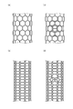
- the single-walled carbon nanotube before the rearrangement structure is introduced has a structure of a carbon six-membered ring network as shown in FIG. 1 (a).
- a carbon five-membered ring structure and a carbon seven-membered ring structure which is a rearrangement structure are introduced into the carbon six-membered ring network of the zigzag single-walled carbon nanotube, a structure as shown in FIG. 1 (b) is obtained.
- the single-walled carbon nanotube before the rearrangement structure is introduced has a structure of a carbon six-membered ring network as shown in FIG. It has become.
- a carbon five-membered ring structure and a carbon seven-membered ring structure, which are rearrangement structures are introduced into the carbon six-membered ring network of this armchair single-walled carbon nanotube, a structure as shown in FIG. 1D is obtained.
- FIG. 1 is a partially enlarged view schematically showing the structure of a single-walled carbon nanotube, and FIG.
- FIG. 1A shows the case where the single-walled carbon nanotube has a zigzag shape
- FIG. The figure shows the case where the rearrangement structure is introduced into the zigzag single-walled carbon nanotube
- the figure (c) shows the case where the single-walled carbon nanotube is an armchair type
- the figure (d) shows the armchair type.
- transduced into a single-walled carbon nanotube is shown.
- the single-walled carbon nanotube may have an open structure at one or both ends of the single-walled carbon nanotube, or may have a closed structure.
- a carbon five-membered ring structure is incorporated at the end of the single-walled carbon nanotube.
- the shape of the tip can be suitably changed according to the number and arrangement position of the carbon five-membered ring structure.
- the carbon five-membered ring structure introduced to make the end of the single-walled carbon nanotube closed is not formed by rearranging the carbon atoms of the vacancy defects. Therefore, it differs from the five-membered carbon ring structure which is the rearrangement structure referred to in the present invention.
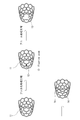
- FIG. 2 is an explanatory view for explaining a method of manufacturing the carbon material.
- the method for producing a carbon material of the present embodiment includes at least a fluorination treatment step of the carbon material and an annealing step of annealing the carbon material after the fluorination treatment.
- the fluorination treatment step is a step of fluorinating the surface of the carbon material in a gas phase by bringing a carbon material into contact with a treatment gas containing at least a fluorine-containing gas.
- a fluorine-containing gas For example, as shown in FIG. 2, when the carbon material is a single-walled carbon nanotube 11, this step is to introduce a fluorine group 12 by a carbon-fluorine bond on the surface of the single-walled carbon nanotube 11.
- This process is different from, for example, an oxidation treatment which imparts an oxygen-containing functional group such as a hydroxyl group, a carbonyl group or a carboxyl group to an edge portion of a carbon hexagonal network surface, and structural defects such as damaging or decomposing carbon materials
- the surface can be fluorinated without being generated.
- a gas containing 0.01 to 100 vol%, preferably 0.1 to 80 vol%, more preferably 1 to 50 vol% of a fluorine-containing gas based on the total volume is used.
- concentration of the fluorine-containing gas By setting the concentration of the fluorine-containing gas to 0.01 vol% or more, the fluorination of the surface of the carbon material can be prevented from becoming insufficient.
- the fluorine-containing gas means a gas containing a fluorine atom, and in the present embodiment, it is not particularly limited as long as it contains a fluorine atom.
- the fluorine-containing gas include fluorine (F 2 ), hydrogen fluoride (HF), chlorine trifluoride (ClF 3 ), sulfur tetrafluoride (SF 4 ), boron trifluoride (BF 3 ), and the like.
- Nitrogen fluoride (NF 3 ), carbonyl fluoride (COF 2 ) and the like can be mentioned. You may use these individually or in mixture of 2 or more types.
- the process gas may contain an inert gas.
- the inert gas is not particularly limited, however, those that react with the fluorine-containing gas to adversely affect the fluorination treatment of the carbon material, those that react with the carbon material to adversely affect, and those containing impurities that cause the adverse effect include Not desirable. Specifically, for example, nitrogen, argon, helium, neon, krypton, xenon and the like can be mentioned. These can be used alone or in combination of two or more. Further, the purity of the inert gas is not particularly limited, but the impurity giving the adverse effect is preferably 100 ppm or less, more preferably 10 ppm or less, and particularly preferably 1 ppm or less.
- the processing gas does not contain a gas containing an oxygen atom.
- a gas containing an oxygen atom By containing the gas containing an oxygen atom, a hydroxyl group, a carboxyl group, etc. may be introduce
- the gas containing an oxygen atom means oxygen gas and nitric acid gas.
- the method for contacting the processing gas is not particularly limited.
- the method can be performed by contacting the carbon material under the flow of the processing gas or in the atmosphere of the processing gas in a sealed container.
- the treatment temperature for the fluorination treatment is not particularly limited, but is preferably in the range of 0 ° C. to 1500 ° C., more preferably 0 ° C. to 800 ° C., still more preferably 0 ° C. to 600 ° C.
- the treatment temperature By setting the treatment temperature to 0 ° C. or higher, the fluorination treatment can be promoted.
- by setting the treatment temperature to 1500 ° C. or less it is possible to suppress an excessive increase of defects in the carbon skeleton generated with the introduction of the fluorine group to the surface of the carbon material, and to excessively destroy the carbon skeleton and It is possible to prevent the mechanical strength of the carbon material from decreasing. Furthermore, thermal deformation can be prevented from occurring in the carbon material, and a decrease in yield can be suppressed.
- the treatment time (reaction time) of the fluorination treatment is not particularly limited, but is in the range of 1 second to 24 hours, preferably 1 second to 12 hours, more preferably 1 second to 9 hours. By setting the treatment time to 1 second or more, the fluorination of the surface of the carbon material can be made sufficient. On the other hand, by setting the treatment time to 24 hours or less, it is possible to prevent the reduction of the production efficiency due to the prolonged production time.
- the pressure condition at the time of performing the fluorination treatment there is no particular limitation on the pressure condition at the time of performing the fluorination treatment, and it can be carried out under normal pressure, under pressure or under reduced pressure. From the viewpoint of economy and safety, it is preferable to carry out under normal pressure. It does not specifically limit as a reaction container for performing a fluorination process, Conventionally well-known things, such as a fixed bed and a fluidized bed, are employable.
- the annealing treatment step is a step of heating the carbon material after the fluorination treatment step at a predetermined temperature.
- a predetermined temperature for example, in the case of the single-walled carbon nanotube 11 shown in FIG. 2, first, the fluorine group 12 introduced to the surface of the single-walled carbon nanotube 11 is eliminated to generate the vacancy defects 13 in the carbon six-membered ring structure. Thereafter, the carbon atoms in the vacancy defects 13 are rearranged to introduce a carbon five-membered ring structure 14 and a carbon seven-membered ring structure 15.
- the treatment temperature at the time of the annealing treatment is in the range of 400 ° C. to 1500 ° C., preferably 600 ° C. to 1500 ° C., more preferably 800 ° C. to 1500 ° C.
- the annealing temperature is set to 400 ° C. or higher.
- the fluorine group can be sufficiently eliminated to promote the formation of a rearranged structure.
- the annealing temperature is set to 1500 ° C. or less, excessive introduction of new structural defects in the carbon six-membered ring network is suppressed, excessive destruction of the carbon skeleton, and mechanical of the carbon material. It is possible to prevent the target strength from decreasing. Furthermore, thermal deformation can be prevented from occurring in the carbon material, and a decrease in yield can be suppressed.
- the treatment time for the annealing treatment is not particularly limited, but is in the range of 1 second to 24 hours, preferably 1 second to 12 hours, more preferably 1 second to 9 hours.
- the treatment time is set to 1 second or more, the fluorine group can be sufficiently eliminated to promote the formation of a rearranged structure.
- the treatment time is set to 24 hours or less, deterioration of the carbon material can be prevented.
- the atmospheric pressure means the pressure (standard atmospheric pressure) in the vicinity of the atmospheric standard condition
- the atmospheric standard condition means the temperature in the vicinity of about 25 ° C. and the atmospheric pressure condition in the vicinity of 101 kPa in absolute pressure.
- the term "atmospheric pressure" also includes cases where the pressure is slightly positive or negative with respect to the standard atmospheric pressure.
- the processing conditions are different in the step of removing the fluorine group from the carbon material to generate a vacancy defect and the step of rearranging the carbon atoms to introduce a rearranged structure, respectively.
- a fluorine group may remain as long as it does not affect the electrical conductivity.
- the manufacturing method of the present embodiment it is possible to manufacture a carbon material in which a five-membered ring structure and a seven-membered ring structure, which are rearranged structures, are incorporated in a carbon six-membered ring network.
- a carbon material having excellent electrical conductivity as compared to a conventional carbon material having a vacancy defect.
- the electrical conductivity (S / m) under reduced pressure is improved by 10% or more with respect to the electrical conductivity (S / m) under atmospheric pressure, for example.
- the carbon material of the present embodiment can be used, for example, as an electron emission material.
- the electron emission material can be applied to an emitter of a field electron emission display (FED), a field effect transistor, a cathode ray tube, an electron gun and the like.
- FED field electron emission display
- field effect transistor field effect transistor
- cathode ray tube cathode ray tube
- electron gun electron gun
- the present invention is not limited to this embodiment.
- the fluorination treatment and the annealing treatment may be performed simultaneously in one step. Thereby, the production time of the carbon material can be shortened.
- the processing conditions in the case of simultaneously performing the fluorination treatment and the annealing treatment are as described above.
- Example 1 10 mg of armchair type (semiconductor type) single-walled carbon nanotubes were introduced into a PTFE (polytetrafluoroethylene) container (volume 5 mL), and this container was placed in a chamber (volume 30 mL) made of electropolished SUS316L.
- PTFE polytetrafluoroethylene
- a chamber volume 30 mL
- electropolished SUS316L As a single-walled carbon nanotube, one having a structure in which both ends are closed was used. Further, the temperature in the chamber was raised to 250 ° C. at a temperature rising rate of 4 ° C./min under a nitrogen gas flow (20 mL / min), and then a constant temperature treatment was performed at a temperature of 250 ° C. for 1 hour.
- the inside of the chamber was vacuum-replaced with a processing gas, and the processing gas was flowed at a flow rate of 25 mL / min to perform fluorination processing.
- the treatment time of the fluorination treatment was 4 hours.
- a mixed gas of fluorine (F 2 ) gas and nitrogen gas was used as the processing gas.
- the concentration of fluorine gas was set to 20 vol% with respect to the total volume of the processing gas.
- the inside of the chamber was vacuum-replaced with nitrogen gas, and allowed to cool to room temperature under a nitrogen stream (20 mL / min), and then the single-walled carbon nanotube after fluorination treatment was taken out from the chamber.
- the single-walled carbon nanotube after the fluorination treatment was placed in an alumina container, and the container was placed in an electric tube furnace to perform vacuum annealing. That is, the inside of the electric tube furnace was evacuated to 1.0 ⁇ 10 ⁇ 5 Pa, and the temperature was raised to 450 ° C. at a temperature rising rate of 3.5 ° C./min under the pressure conditions. After the temperature rise, a constant temperature treatment was performed at 450 ° C. for 1 hour. By raising the temperature to 450 ° C. and high-temperature treatment at 450 ° C. for 1 hour, the fluorine group was detached from the single-walled carbon nanotube to generate a vacancy defect. Subsequently, the temperature was raised to 1200 ° C.
- Comparative example 1 In this comparative example, only the vacuum annealing process was performed on the armchair-type (semiconductor-type) single-walled carbon nanotube without performing the fluorination process.
- a single-walled carbon nanotube according to this comparative example was manufactured in the same manner as in Example 1 except for the above.
- a single-walled carbon nanotube one having a structure in which both ends are closed was used.
- the conductivity of the thin film sample under reduced pressure was measured by the four-terminal method. That is, gold electrodes were attached so as to abut the four corners of each thin film sample, and lead wires from each gold electrode were attached to the sample holder. Subsequently, a sample holder provided with each thin film sample was placed in the chamber, and the inside of the chamber was evacuated to 1.0 ⁇ 10 ⁇ 5 Pa by a rotary pump. Thereafter, the inside of the chamber was heat-treated at 300 ° C. under reduced pressure to remove oxygen atoms adsorbed to the thin film sample.
Landscapes
- Engineering & Computer Science (AREA)
- Chemical & Material Sciences (AREA)
- Nanotechnology (AREA)
- Materials Engineering (AREA)
- Crystallography & Structural Chemistry (AREA)
- Organic Chemistry (AREA)
- Power Engineering (AREA)
- Physics & Mathematics (AREA)
- Condensed Matter Physics & Semiconductors (AREA)
- General Physics & Mathematics (AREA)
- Manufacturing & Machinery (AREA)
- Microelectronics & Electronic Packaging (AREA)
- Inorganic Chemistry (AREA)
- Composite Materials (AREA)
- Carbon And Carbon Compounds (AREA)
- Cold Cathode And The Manufacture (AREA)
- Conductive Materials (AREA)
Abstract
電気伝導性に優れた炭素材料、その製造方法及び電子放出材料を提供する。 本発明にかかる炭素材料は、炭素六員環ネットワークを有する炭素材料であって、前記炭素六員環ネットワーク中に、再配列構造である炭素五員環構造と炭素七員環構造がそれぞれ組み込まれていることを特徴とする。
Description
本発明は、炭素材料、その製造方法及び電子放出材料に関し、より詳細には導電性に優れ、電界電子放出型ディスプレイ(FED)のエミッタや電界効果トランジスタ、陰極線管、電子銃等の電子デバイスへの応用が可能な炭素材料、その製造方法及び電子放出材料に関する。
単層カーボンナノチューブ(single-walled carbon nanotubes、以下「SWCNT」という場合がある。)は炭素原子のみから構成される中空円筒状の炭素材料であり、その特徴的な構造ゆえに優れた機械特性や電気伝導性を示す。また、SWCNTは巻き方(カイラリティ)によって金属型にも半導体型にもなるという特異な性質を備えている。特に、その優れた電気伝導性を活かしてナノ配線や超軽量電線、その他電子デバイスへの応用が期待されているが、未だ実現には至っていない。
その原因の一つとして、SWCNTの合成過程、精製過程又は表面の化学修飾過程等で、その炭素骨格に構造上の欠陥が導入されることが挙げられる。構造上の欠陥は、SWCNTの電気伝導性をはじめとする幾つかの特性の低下又は変化を招来するためである。その結果、構造欠陥を有しないSWCNTの研究・開発が進められているが、その合成は困難であるという問題がある。尚、ここでいう構造上の欠陥とは、導入された官能基、STW(Stone-Thrower-Wales)欠陥、炭素原子以外の原子(例えば、水素原子や酸素原子、窒素原子、金属原子等)が存在することによる欠陥、空孔欠陥等を意味する。
本発明は前記問題点に鑑みなされたものであり、その目的は、電気伝導性に優れた炭素材料、その製造方法及び電子放出材料を提供することにある。
本願発明者等は、SWCNT等の炭素材料を実用化するにあたって、空孔欠陥が発生するのを防止するのではなく、当該空孔欠陥を積極的に利用することで、電気伝導性等の特性の制御が可能になることを見出し、本願発明を完成させるに至った。
すなわち、本発明の炭素材料は、前記の課題を解決する為に、炭素六員環ネットワークを有する炭素材料であって、前記炭素六員環ネットワーク中に、再配列構造である炭素五員環構造と炭素七員環構造がそれぞれ組み込まれているものであることを特徴とする。
前記の構成に於いて、前記炭素六員環ネットワークを有する炭素材料がカーボンナノチューブであり、前記再配列構造である炭素五員環構造と炭素七員環構造が、前記カーボンナノチューブの少なくとも側面にそれぞれ組み込まれていることが好ましい。
前記の構成に於いては、前記カーボンナノチューブが、ジグザグ型単層カーボンナノチューブ、アームチェア型単層カーボンナノチューブ又はキラル型単層カーボンナノチューブであることが好ましい。
前記の構成に於いては、前記炭素六員環ネットワークを有する炭素材料がグラフェンであることが好ましい。
本発明に係る炭素材料の製造方法は、前記の課題を解決する為に、炭素六員環ネットワークを有する炭素材料に、フッ素含有ガスを含む処理ガスを接触させて、当該炭素材料の表面にフッ素基を導入するフッ素化処理工程と、前記フッ素化処理工程後の炭素材料を、温度400℃~1500℃の条件下でアニール処理することにより、前記フッ素基を脱離させて炭素六員環構造に空孔を生じさせ、再配列構造である炭素五員環構造と炭素七員環構造をそれぞれ導入するアニール処理工程とを含むことを特徴とする。
前記の構成に於いては、前記炭素六員環ネットワークを有する炭素材料としてカーボンナノチューブを用い、前記アニール処理により、前記再配列構造である炭素五員環構造と炭素七員環構造を、前記カーボンナノチューブの側面にそれぞれ導入することが好ましい。
前記の構成に於いては、前記カーボンナノチューブとして、ジグザグ型単層カーボンナノチューブ、アームチェア型単層カーボンナノチューブ又はキラル型単層カーボンナノチューブを用いることが好ましい。
前記の構成に於いては、前記炭素六員環ネットワークを有する炭素材料としてグラフェンを用いたことが好ましい。
本発明の炭素材料によれば、これを構成する炭素六員環ネットワーク中には、炭素五員環構造及び炭素七員環構造がそれぞれ組み込まれている。そして、炭素五員環構造及び炭素七員環構造は、本来、空孔欠陥が生じていた部分の炭素原子を再配列させた構造である。そのため、前記構成の炭素材料は、空孔欠陥を有する炭素材料と比較して、電気伝導性の向上を図ることができる。
また、本発明の炭素材料の製造方法によれば、炭素六員環ネットワークを有する炭素材料にフッ素含有ガスを含む処理ガスを接触させることにより、炭素材料の表面にフッ素基を導入してフッ素化処理を行う。次いで、アニール処理を行うことでフッ素基を脱離させ、炭素六員環ネットワークに空孔欠陥を生じさせた後に、当該空孔欠陥部分の炭素原子を再配列させる。これにより、炭素六員環ネットワーク中に再配列構造である炭素五員環構造及び炭素七員環構造が導入され、電気伝導性に優れた炭素材料の製造が可能になる。
(炭素材料)
本発明の実施の一形態に係る炭素材料について、以下に説明する。
本実施の形態の炭素材料は、炭素六員環ネットワークを有し、さらに炭素六員環ネットワークに再配列構造である炭素五員環構造と炭素七員環構造がそれぞれ組み込まれた構造を有する。炭素骨格である炭素六員環ネットワーク中に、炭素五員環構造及び炭素七員環構造が組み込まれることにより、当該炭素材料の電気伝導性の向上が図れる。
本発明の実施の一形態に係る炭素材料について、以下に説明する。
本実施の形態の炭素材料は、炭素六員環ネットワークを有し、さらに炭素六員環ネットワークに再配列構造である炭素五員環構造と炭素七員環構造がそれぞれ組み込まれた構造を有する。炭素骨格である炭素六員環ネットワーク中に、炭素五員環構造及び炭素七員環構造が組み込まれることにより、当該炭素材料の電気伝導性の向上が図れる。
本発明において「炭素六員環ネットワーク」とは、炭素原子のみで構成される六員環構造(ハニカム構造)を一単位として、当該六員環構造がネットワーク状に結合した炭素骨格を意味する。「炭素六員環ネットワーク」は水素原子及び置換基を含まない骨組みであって、全て炭素原子からなる。また、本発明において「再配列構造」とは、炭素六員環ネットワークに存在していた空孔欠陥部分において、炭素原子を再配列させたことにより形成される構造を意味し、より具体的には炭素五員環構造及び炭素七員環構造をいう。さらに、前記「空孔欠陥」とは、炭素六員環ネットワークにおいて、当該ネットワークを構成する炭素原子の一部が存在せず、構造上の欠陥として空孔が生じた状態を意味する。
前記炭素材料としては、炭素原子からなる炭素六員環ネットワークを備えるものであれば特に限定されず、例えば、活性炭、カーボンナノコイル、グラファイト、カーボンブラック、ダイヤモンドライクカーボン、炭素繊維、グラフェン、非晶質カーボン、フラーレン、カーボンナノチューブ等が挙げられる。さらに、このような炭素材料の基本構造を有する類縁体も本発明にかかる炭素材料に含まれる。これらの炭素材料のうち本実施の形態においては、カーボンナノチューブやグラフェン等が好ましい。尚、フラーレンは、炭素六員環構造の他に炭素五員環構造を本来的に有するものであるが、当該炭素五員環構造は炭素六員環ネットワークに存在していた空孔欠陥部分の炭素原子を再配列させたことにより形成されるものではない。従って、本発明にいう再配列構造である炭素五員環構造とは異なる。
炭素材料がカーボンナノチューブである場合、再配列構造である炭素五員環構造及び炭素七員環構造は、当該カーボンナノチューブの少なくとも側面に組み込まれる。カーボンナノチューブの側面に再配列構造である炭素五員環構造及び炭素七員環構造を組み込むことにより、カーボンナノチューブの電気伝導性の向上が図れる。
前記カーボンナノチューブとしては、6角網目のチューブ(グラフェンシート)が1枚の構造である単層カーボンナノチューブ(SWCNT:Single Wall Carbon Nanotube)や、多層のグラフェンシートから構成されている多層カーボンナノチューブ(MWCNT:Maluti Wall Carbon Nanotube)、フラーレンチューブ、バッキーチューブ、グラファイトフィブリルが挙げられる。
さらに、単層カーボンナノチューブとしては、六員環構造の配列の観点から、ジグザグ型(金属型)単層カーボンナノチューブ、アームチェア型(半導体型)単層カーボンナノチューブ、キラル型単層カーボンナノチューブが挙げられる。
単層カーボンナノチューブがジグザグ型(金属型)である場合、再配列構造が導入される前の単層カーボンナノチューブは、図1(a)に示すような炭素六員環ネットワークの構造となっている。このジグザグ型単層カーボンナノチューブの炭素六員環ネットワークに、再配列構造である炭素五員環構造及び炭素七員環構造が導入されると、図1(b)に示す様な構造となる。また、単層カーボンナノチューブがアームチェア型(半導体型)である場合、再配列構造が導入される前の単層カーボンナノチューブは、図1(c)に示すような炭素六員環ネットワークの構造となっている。このアームチェア型単層カーボンナノチューブの炭素六員環ネットワークに、再配列構造である炭素五員環構造及び炭素七員環構造が導入されると、図1(d)に示す様な構造となる。尚、図1は、単層カーボンナノチューブの構造を概略的に表す部分拡大図であって、同図(a)は単層カーボンナノチューブがジグザグ型である場合を表し、同図(b)は当該ジグザグ型の単層カーボンナノチューブに再配列構造が導入された場合を表し、同図(c)は単層カーボンナノチューブがアームチェア型である場合を表し、同図(d)は当該アームチェア型の単層カーボンナノチューブに再配列構造が導入された場合を表す。
単層カーボンナノチューブは、その末端の一方又は両方が開放された構造であってもよく、あるいは閉鎖された構造であってもよい。閉鎖された構造である場合には、単層カーボンナノチューブの末端に炭素五員環構造が組み込まれる。この場合、その先端形状は炭素五員環構造の数や配置位置に応じて適宜変更可能である。尚、単層カーボンナノチューブの末端を閉鎖した構造とするために導入される炭素五員環構造は、空孔欠陥部分の炭素原子を再配列させて形成されるものではない。従って、本発明にいう再配列構造である炭素五員環構造とは異なる。
(炭素材料の製造方法)
次に、本実施の形態に係る炭素材料の製造方法について、図2に基づき以下に説明する。図2は、前記炭素材料の製造方法を説明するための説明図である。
次に、本実施の形態に係る炭素材料の製造方法について、図2に基づき以下に説明する。図2は、前記炭素材料の製造方法を説明するための説明図である。
図2に示すように、本実施の形態の炭素材料の製造方法は、炭素材料のフッ素化処理工程と、フッ素化処理後の炭素材料をアニール処理するアニール処理工程とを少なくとも有する。
前記フッ素化処理工程は、炭素材料に少なくともフッ素含有ガスを含む処理ガスを接触させることにより、気相中でその表面をフッ素化処理する工程である。例えば、図2に示すように、炭素材料が単層カーボンナノチューブ11である場合、本工程は単層カーボンナノチューブ11の表面に炭素-フッ素結合によるフッ素基12を導入するものである。本工程は、例えば、炭素六角網面のエッジ部分に水酸基、カルボニル基又はカルボキシル基等の含酸素官能基を付与する酸化処理とは異なり、炭素材料にダメージを与えたり分解させる等の構造欠陥を生じさせることなく、その表面をフッ素化することができる。
前記処理ガスとしては、全体積に対し0.01~100vol%、好ましくは0.1~80vol%、より好ましくは1~50vol%のフッ素含有ガスを含むものが用いられる。フッ素含有ガスの濃度を0.01vol%以上にすることにより、炭素材料表面のフッ素化が不十分となるのを防止することができる。
前記フッ素含有ガスとはフッ素原子を含む気体を意味し、本実施の形態に於いてはフッ素原子を含むものであれば特に限定されない。前記フッ素含有ガスとしては、例えば、フッ素(F2)、フッ化水素(HF)、三フッ化塩素(ClF3)、四フッ化硫黄(SF4)、三フッ化ホウ素(BF3)、三フッ化窒素(NF3)、フッ化カルボニル(COF2)等が挙げられる。これらは単独で、又は二種以上を混合して用いてもよい。
前記処理ガスには不活性ガスが含まれていてもよい。不活性ガスとしては特に限定されないが、フッ素含有ガスと反応して炭素材料のフッ素化処理に悪影響を与えるもの、炭素材料と反応して悪影響を与えるもの、及び当該悪影響を与える不純物を含むものは好ましくない。具体的には、例えば、窒素、アルゴン、ヘリウム、ネオン、クリプトン、キセノン等が挙げられる。これらは単独で、又は2種以上を混合して用いることができる。また、不活性ガスの純度としては特に限定されないが、当該悪影響を与える不純物については100ppm以下であることが好ましく、10ppm以下であることがより好ましく、1ppm以下であることが特に好ましい。
尚、前記処理ガス中には酸素原子を含むガスを含まないことが好ましい。酸素原子を含むガスを含有させることにより、炭素材料の表面に水酸基やカルボキシル基等が導入され、炭素材料に大きなダメージを与える場合があるからである。尚、酸素原子を含むガスとは、酸素ガスや硝酸ガスを意味する。
処理ガスの接触方法としては特に限定されず、例えば、処理ガスのフロー下で、又は密閉状態にした容器内の、当該処理ガスの雰囲気下で、炭素材料に接触させることにより行うことができる。
前記フッ素化処理を行う際の処理温度は特に限定されないが、好ましくは0℃~1500℃の範囲内であり、より好ましくは0℃~800℃、さらに好ましくは0℃~600℃である。処理温度を0℃以上にすることにより、フッ素化処理の促進が図られる。その一方、処理温度を1500℃以下にすることにより、炭素材料表面へのフッ素基の導入に伴って発生する炭素骨格への欠陥が過度に増大するのを抑制し、炭素骨格の過度の破壊及び炭素材料の機械的強度が減少するのを防止することができる。さらに、炭素材料に熱変形が生じるのを防止し、歩留まりの低下を抑制することができる。
前記フッ素化処理の処理時間(反応時間)は特に限定されないが、1秒~24時間の範囲内であり、好ましくは1秒~12時間、より好ましくは1秒~9時間である。処理時間を1秒以上にすることにより、炭素材料表面のフッ素化を十分なものにすることができる。その一方、処理時間を24時間以下にすることにより、製造時間の長期化による製造効率の低下を防止することができる。
フッ素化処理を行う際の圧力条件としては特に限定されず、常圧下、加圧下又は減圧下で行うことができる。経済上・安全上の観点からは、常圧下で行うのが好ましい。フッ素化処理を行うための反応容器としては特に限定されず、固定床、流動床等の従来公知のものを採用することができる。
炭素材料に対する処理ガスの接触方法としては特に限定されず、例えば、当該処理ガスのフロー下で接触させることができる。
前記アニール処理工程は、フッ素化処理工程後の炭素材料を所定の温度で加熱する工程である。例えば、図2に示す単層カーボンナノチューブ11の場合、先ず、当該単層カーボンナノチューブ11の表面に導入されたフッ素基12を脱離させて炭素六員環構造に空孔欠陥13を生じさせる。その後、空孔欠陥13における炭素原子を再配列させ、炭素五員環構造14及び炭素七員環構造15を導入する。
アニール処理を行う際の処理温度は400℃~1500℃の範囲内であり、好ましくは600℃~1500℃、より好ましくは800℃~1500℃である。アニール処理の温度を400℃以上にすることにより、フッ素基を十分に脱離させ、再配列構造の生成を促進することができる。その一方、アニール処理の温度を1500℃以下にすることにより、炭素六員環ネットワークに新たな構造上の欠陥が過度に導入されるのを抑制し、炭素骨格の過度の破壊及び炭素材料の機械的強度が減少するのを防止することができる。さらに、炭素材料に熱変形が生じるのを防止し、歩留まりの低下を抑制することができる。
前記アニール処理を行う際の処理時間は特に限定されないが、1秒~24時間の範囲内であり、好ましくは1秒~12時間、より好ましくは1秒~9時間である。処理時間を1秒以上にすることにより、フッ素基を十分に脱離させ、再配列構造の生成を促進することが可能になる。その一方、処理時間を24時間以下にすることにより、炭素材料の劣化を防止することができる。
前記アニール処理を行う際の圧力条件としては特に限定されないが、大気圧に対し減圧下又は高真空下で行うことが好ましい。圧力条件を大気圧よりも減圧下にすることにより、フッ素基の脱離による空孔欠陥の生成を促進することができる。尚、大気圧とは、大気の標準状態近傍における圧力(標準大気圧)のことを意味し、大気の標準状態とは、約25℃近傍の温度、絶対圧で101kPa近傍の大気圧条件のことを意味する。さらに、前記「大気圧」には標準大気圧に対し僅かに陽圧又は陰圧の場合も含む。
また、アニール処理工程は、炭素材料からフッ素基を脱離させて空孔欠陥を生じさせる段階と、その後、炭素原子を再配列させて再配列構造を導入する段階とで、それぞれ処理条件を異ならせてもよい。
また、アニール処理工程後の炭素材料について、電気伝導性の向上の観点からはフッ素基が残存していないことが望ましいが、例えば、当該炭素材料の溶媒への分散性の向上等の機能を付与したい場合には、電気伝導性への影響を及ぼさない範囲でフッ素基が残存していてもよい。
以上より、本実施の形態の製造方法であると、炭素六員環ネットワーク中に、再配列構造である五員環構造及び七員環構造が組み込まれた炭素材料を製造することができる。これにより、本実施の形態においては、空孔欠陥を有する従来の炭素材料と比較して、電気伝導性に優れた炭素材料を製造することができる。
尚、炭素材料の電気伝導性は、例えば、大気圧下における電気伝導率(S/m)に対して減圧下での電気伝導率(S/m)が10%以上向上していることが好ましく、好ましくは20%以上、より好ましくは40%以上である。
(電子放出材料)
本実施の形態の炭素材料は、例えば、電子放出材料として利用可能である。電子放出材料は電界電子放出型ディスプレイ(FED)のエミッタ、電界効果トランジスタ、陰極線管、電子銃等に適用することができる。
本実施の形態の炭素材料は、例えば、電子放出材料として利用可能である。電子放出材料は電界電子放出型ディスプレイ(FED)のエミッタ、電界効果トランジスタ、陰極線管、電子銃等に適用することができる。
(その他)
本実施の形態においては、フッ素化処理工程後にアニール処理工程を行う態様について説明した。但し、本発明はこの態様に限定されるものではなく、例えば、フッ素化処理とアニール処理を1つの工程中に同時に行ってもよい。これにより、炭素材料の製造時間の短縮化が図れる。尚、フッ素化処理とアニール処理を同時に行う場合の処理条件については、前述の通りである。
本実施の形態においては、フッ素化処理工程後にアニール処理工程を行う態様について説明した。但し、本発明はこの態様に限定されるものではなく、例えば、フッ素化処理とアニール処理を1つの工程中に同時に行ってもよい。これにより、炭素材料の製造時間の短縮化が図れる。尚、フッ素化処理とアニール処理を同時に行う場合の処理条件については、前述の通りである。
(実施例1)
PTFE(ポリテトラフルオロエチレン)容器(容量5mL)に、アームチェア型(半導体型)の単層カーボンナノチューブ10mgを導入し、本容器を電解研磨されたSUS316L製チャンバー(容量30mL)に設置した。単層カーボンナノチューブとしては、両端が閉鎖された構造のものを用いた。更に、チャンバー内を、窒素ガスの気流(20mL/min)下で、4℃/minの昇温速度で250℃まで昇温した後、温度250℃で1時間の恒温処理を行った。
PTFE(ポリテトラフルオロエチレン)容器(容量5mL)に、アームチェア型(半導体型)の単層カーボンナノチューブ10mgを導入し、本容器を電解研磨されたSUS316L製チャンバー(容量30mL)に設置した。単層カーボンナノチューブとしては、両端が閉鎖された構造のものを用いた。更に、チャンバー内を、窒素ガスの気流(20mL/min)下で、4℃/minの昇温速度で250℃まで昇温した後、温度250℃で1時間の恒温処理を行った。
次に、チャンバー内を処理ガスに真空置換し、流量25mL/minで処理ガスを流して、フッ素化処理をした。フッ素化処理の処理時間は4時間とした。また、処理ガスとしては、フッ素(F2)ガスと窒素ガスの混合ガスを用いた。さらに、フッ素ガスの濃度は処理ガスの全体積に対し20vol%とした。フッ素化処理後、チャンバー内を窒素ガスに真空置換し、窒素気流(20mL/min)の下、室温まで放冷し、その後、チャンバーからフッ素化処理後の単層カーボンナノチューブを取り出した。
次に、アルミナ容器にフッ素化処理後の単層カーボンナノチューブを入れ、本容器を電気管状炉内に設置して真空アニール処理を行った。すなわち、電気管状炉内を1.0×10⁻⁵Paまで真空引きし、当該圧力条件下で、昇温速度3.5℃/minにて、450℃まで昇温させた。昇温後、450℃で1時間の恒温処理を行った。この450℃までの昇温と、450℃・1時間での高温処理とにより、単層カーボンナノチューブからフッ素基を脱離させ、空孔欠陥を生成させた。続いて、前記圧力条件下で、昇温速度2.5℃/minにて、1200℃まで昇温させた。昇温後、温度1200℃で3時間の恒温処理を行った。この1200℃までの昇温と、1200℃・3時間での高温処理とにより、単層カーボンナノチューブに生成させた空孔欠陥における炭素原子を再配列させて再配列構造を導入した。その後、電気管状炉内を室温まで放冷した後、チャンバー内を窒素ガスに置換し、本実施例に係る単層カーボンナノチューブを製造した。
(比較例1)
本比較例においては、アームチェア型(半導体型)の単層カーボンナノチューブに対し、フッ素化処理を行わず真空アニール処理のみを行った。それ以外は、実施例1と同様にして本比較例に係る単層カーボンナノチューブを製造した。尚、単層カーボンナノチューブとしては、両端が閉鎖された構造のものを用いた。
本比較例においては、アームチェア型(半導体型)の単層カーボンナノチューブに対し、フッ素化処理を行わず真空アニール処理のみを行った。それ以外は、実施例1と同様にして本比較例に係る単層カーボンナノチューブを製造した。尚、単層カーボンナノチューブとしては、両端が閉鎖された構造のものを用いた。
(元素分析)
処理前の単層カーボンナノチューブ、並びに実施例1及び比較例1に係る単層カーボンナノチューブのそれぞれについて、X線光電子分光法(Thermo Fisher Scientific社製、商品名:K-Alpha)を用いて元素分析を行った。
処理前の単層カーボンナノチューブ、並びに実施例1及び比較例1に係る単層カーボンナノチューブのそれぞれについて、X線光電子分光法(Thermo Fisher Scientific社製、商品名:K-Alpha)を用いて元素分析を行った。
(電気伝導性の評価)
<大気下での導電率測定>
処理前の単層カーボンナノチューブ、並びに実施例1及び比較例1に係る単層カーボンナノチューブのそれぞれについて、5mgを50mLのエタノール中に入れ、15分間の超音波処理を実施して分散液を調製した。その後、分散液を減圧濾過し、縦1cm×横1cm×厚さ0.5mmの薄膜サンプルを作製した。
処理前の単層カーボンナノチューブ、並びに実施例1及び比較例1に係る単層カーボンナノチューブのそれぞれについて、5mgを50mLのエタノール中に入れ、15分間の超音波処理を実施して分散液を調製した。その後、分散液を減圧濾過し、縦1cm×横1cm×厚さ0.5mmの薄膜サンプルを作製した。
続いて、それぞれの薄膜サンプルの四隅に金電極が当接するように取り付け、さらに各金電極からリード線を試料ホルダーに取り付けた。そして、4端子法により各薄膜サンプルの比抵抗を測定し、電気伝導率を算出した。測定は、大気圧下、気温25℃、相対湿度35%の条件で行った。測定の結果を下記表1に示す。
<真空下における導電率測定>
また、前記薄膜サンプルの減圧下での導電率について、4端子法により測定を行った。すなわち、各薄膜サンプルの四隅に金電極が当接するように取り付け、さらに各金電極からリード線を試料ホルダーに取り付けた。続いて、各薄膜サンプルを備えた試料ホルダーをそれぞれチャンバー内に入れ、ロータリーポンプでチャンバー内を1.0×10⁻⁵Paまで真空引きした。その後、チャンバー内を減圧条件下で300℃にて加熱処理し、薄膜サンプルに吸着している酸素原子を除去した。続いて、減圧条件下でチャンバー内を室温まで冷却し、4端子法により各薄膜サンプルの比抵抗を測定し、電気伝導率を算出した。測定は、圧力1.0×10⁻⁵Paの下、気温25℃、相対湿度35%の条件で行った。測定の結果を下記表1に示す。
また、前記薄膜サンプルの減圧下での導電率について、4端子法により測定を行った。すなわち、各薄膜サンプルの四隅に金電極が当接するように取り付け、さらに各金電極からリード線を試料ホルダーに取り付けた。続いて、各薄膜サンプルを備えた試料ホルダーをそれぞれチャンバー内に入れ、ロータリーポンプでチャンバー内を1.0×10⁻⁵Paまで真空引きした。その後、チャンバー内を減圧条件下で300℃にて加熱処理し、薄膜サンプルに吸着している酸素原子を除去した。続いて、減圧条件下でチャンバー内を室温まで冷却し、4端子法により各薄膜サンプルの比抵抗を測定し、電気伝導率を算出した。測定は、圧力1.0×10⁻⁵Paの下、気温25℃、相対湿度35%の条件で行った。測定の結果を下記表1に示す。

(結果)
表1から分かる通り、処理前及び比較例1の単層カーボンナノチューブの場合、大気圧下における比抵抗は減圧下における比抵抗と比べ小さい値となっており、大気圧下での導電率が高いことがわかる。一方、本実施例の単層カーボンナノチューブでは、大気圧下における比抵抗が減圧下における比抵抗よりも高い値となっており、減圧下において電気伝導率が45%以上向上していることが確認された。
表1から分かる通り、処理前及び比較例1の単層カーボンナノチューブの場合、大気圧下における比抵抗は減圧下における比抵抗と比べ小さい値となっており、大気圧下での導電率が高いことがわかる。一方、本実施例の単層カーボンナノチューブでは、大気圧下における比抵抗が減圧下における比抵抗よりも高い値となっており、減圧下において電気伝導率が45%以上向上していることが確認された。
また、元素分析の結果、処理前、実施例1及び比較例1の各単層カーボンナノチューブのいずれにおいてもフッ素原子は検出されなかった(フッ素原子の原子組成百分率0at%)。このうち、実施例1に係る単層カーボンナノチューブについては、大気圧下の比抵抗と減圧下の比抵抗の値の変化がフッ素基の存在によるものではないことが確認された。その結果、実施例1の単層カーボンナノチューブにおいては、再配列構造である炭素五員環構造と炭素七員環構造が導入されていることが示された。
Claims (9)
- 炭素六員環ネットワークを有する炭素材料であって、
前記炭素六員環ネットワーク中に、再配列構造である炭素五員環構造と炭素七員環構造がそれぞれ組み込まれている炭素材料。 - 前記炭素六員環ネットワークを有する炭素材料がカーボンナノチューブであり、
前記再配列構造である炭素五員環構造と炭素七員環構造が、前記カーボンナノチューブの少なくとも側面にそれぞれ組み込まれている請求項1に記載の炭素材料。 - 前記カーボンナノチューブが、ジグザグ型単層カーボンナノチューブ、アームチェア型単層カーボンナノチューブ又はキラル型単層カーボンナノチューブである請求項2に記載の炭素材料。
- 前記炭素六員環ネットワークを有する炭素材料がグラフェンである請求項1に記載の炭素材料。
- 炭素六員環ネットワークを有する炭素材料に、フッ素含有ガスを含む処理ガスを接触させて、当該炭素材料の表面にフッ素基を導入するフッ素化処理工程と、
前記フッ素化処理工程後の炭素材料を、温度400℃~1500℃の条件下でアニール処理することにより、前記フッ素基を脱離させて炭素六員環構造に空孔を生じさせ、再配列構造である炭素五員環構造と炭素七員環構造をそれぞれ導入するアニール処理工程とを含む炭素材料の製造方法。 - 前記炭素六員環ネットワークを有する炭素材料としてカーボンナノチューブを用い、
前記アニール処理により、前記再配列構造である炭素五員環構造と炭素七員環構造を、前記カーボンナノチューブの側面にそれぞれ導入する請求項5に記載の炭素材料の製造方法。 - 前記カーボンナノチューブとして、ジグザグ型単層カーボンナノチューブ、アームチェア型単層カーボンナノチューブ又はキラル型単層カーボンナノチューブを用いる請求項6に記載の炭素材料の製造方法。
- 前記炭素六員環ネットワークを有する炭素材料としてグラフェンを用いた請求項5に記載の炭素材料の製造方法。
- 請求項1~4の何れか1項に記載の炭素材料を含む電子放出材料。
Priority Applications (1)
| Application Number | Priority Date | Filing Date | Title |
|---|---|---|---|
| JP2018554991A JP7092306B2 (ja) | 2016-12-06 | 2017-12-04 | 炭素材料、その製造方法及び電子放出材料 |
Applications Claiming Priority (2)
| Application Number | Priority Date | Filing Date | Title |
|---|---|---|---|
| JP2016236704 | 2016-12-06 | ||
| JP2016-236704 | 2016-12-06 |
Publications (1)
| Publication Number | Publication Date |
|---|---|
| WO2018105559A1 true WO2018105559A1 (ja) | 2018-06-14 |
Family
ID=62491934
Family Applications (1)
| Application Number | Title | Priority Date | Filing Date |
|---|---|---|---|
| PCT/JP2017/043491 Ceased WO2018105559A1 (ja) | 2016-12-06 | 2017-12-04 | 炭素材料、その製造方法及び電子放出材料 |
Country Status (2)
| Country | Link |
|---|---|
| JP (1) | JP7092306B2 (ja) |
| WO (1) | WO2018105559A1 (ja) |
Cited By (1)
| Publication number | Priority date | Publication date | Assignee | Title |
|---|---|---|---|---|
| US20220371897A1 (en) * | 2021-05-24 | 2022-11-24 | Sgraphene | Graphene nanopore manufacturing method using detachable functional groups and graphene sheet having graphene nanoholes formed thereby |
Citations (6)
| Publication number | Priority date | Publication date | Assignee | Title |
|---|---|---|---|---|
| JP2004352608A (ja) * | 2003-05-28 | 2004-12-16 | Samsung Corning Co Ltd | 炭素ナノ構造体の分散方法 |
| WO2010074000A1 (ja) * | 2008-12-24 | 2010-07-01 | 国立大学法人東北大学 | 炭素材料の分散液、及びその製造方法 |
| JP2013075783A (ja) * | 2011-09-30 | 2013-04-25 | Mitsubishi Materials Corp | フッ素化カーボンナノファイバーとその製造方法および用途 |
| JP2013529176A (ja) * | 2010-06-10 | 2013-07-18 | ザ・ユニバーシティ・オブ・マンチェスター | 機能化されたグラフェン |
| JP2014533973A (ja) * | 2011-09-23 | 2014-12-18 | パルティ、ヨーラム | ナノチューブと人工肺とを備えるガス交換装置 |
| JP2016113364A (ja) * | 2014-12-16 | 2016-06-23 | 国立大学法人東北大学 | 窒素含有炭素材料及びその製造方法 |
-
2017
- 2017-12-04 WO PCT/JP2017/043491 patent/WO2018105559A1/ja not_active Ceased
- 2017-12-04 JP JP2018554991A patent/JP7092306B2/ja active Active
Patent Citations (6)
| Publication number | Priority date | Publication date | Assignee | Title |
|---|---|---|---|---|
| JP2004352608A (ja) * | 2003-05-28 | 2004-12-16 | Samsung Corning Co Ltd | 炭素ナノ構造体の分散方法 |
| WO2010074000A1 (ja) * | 2008-12-24 | 2010-07-01 | 国立大学法人東北大学 | 炭素材料の分散液、及びその製造方法 |
| JP2013529176A (ja) * | 2010-06-10 | 2013-07-18 | ザ・ユニバーシティ・オブ・マンチェスター | 機能化されたグラフェン |
| JP2014533973A (ja) * | 2011-09-23 | 2014-12-18 | パルティ、ヨーラム | ナノチューブと人工肺とを備えるガス交換装置 |
| JP2013075783A (ja) * | 2011-09-30 | 2013-04-25 | Mitsubishi Materials Corp | フッ素化カーボンナノファイバーとその製造方法および用途 |
| JP2016113364A (ja) * | 2014-12-16 | 2016-06-23 | 国立大学法人東北大学 | 窒素含有炭素材料及びその製造方法 |
Non-Patent Citations (1)
| Title |
|---|
| MIZOGUCHI, NORIYUKI: "HOMO-LUMO gaps of armchair carbon nanotubes with Stone-Wales defect", STON-WALES HOMO-LUMO, 6 November 2011 (2011-11-06) * |
Cited By (6)
| Publication number | Priority date | Publication date | Assignee | Title |
|---|---|---|---|---|
| US20220371897A1 (en) * | 2021-05-24 | 2022-11-24 | Sgraphene | Graphene nanopore manufacturing method using detachable functional groups and graphene sheet having graphene nanoholes formed thereby |
| CN115385329A (zh) * | 2021-05-24 | 2022-11-25 | 爱思石墨烯 | 石墨烯纳米孔的形成方法和具有石墨烯纳米孔的石墨烯片 |
| JP2022180266A (ja) * | 2021-05-24 | 2022-12-06 | 株式会社エスグラフェン | 官能基の着脱を利用したグラフェンナノ細孔の形成方法及びそれによって形成されたグラフェンナノ細孔を有するグラフェンシート |
| JP7197095B2 (ja) | 2021-05-24 | 2022-12-27 | 株式会社エスグラフェン | 官能基の着脱を利用したグラフェンナノ細孔の形成方法及びそれによって形成されたグラフェンナノ細孔を有するグラフェンシート |
| CN115385329B (zh) * | 2021-05-24 | 2024-08-20 | 爱思石墨烯 | 石墨烯纳米孔的形成方法和具有石墨烯纳米孔的石墨烯片 |
| US12071348B2 (en) * | 2021-05-24 | 2024-08-27 | Sgraphene | Graphene nanopore manufacturing method using detachable functional groups and graphene sheet having graphene nanoholes formed thereby |
Also Published As
| Publication number | Publication date |
|---|---|
| JP7092306B2 (ja) | 2022-06-28 |
| JPWO2018105559A1 (ja) | 2019-10-24 |
Similar Documents
| Publication | Publication Date | Title |
|---|---|---|
| KR102415010B1 (ko) | 질소 함유 탄소 재료 및 그 제조 방법 | |
| EP1810950B1 (en) | Carbon nanotube aggregate and process for producing the same | |
| US10703632B2 (en) | Method of purifying carbon nanotubes | |
| JP6666866B2 (ja) | カーボンナノチューブ撚糸電線の製造方法 | |
| EP3287415B1 (en) | Cross-linked structure of carbon material and method for producing same | |
| EP2377814A1 (en) | Dispersion of carbon material and process for producing same | |
| CN109311674B (zh) | 碳材料及其制造方法 | |
| Hussain et al. | Growth and plasma functionalization of carbon nanotubes | |
| Mehdi et al. | Enhancing purity and crystallinity of carbon nanotubes by magnetically assisted arc discharge and thermal purification and their field emission characteristics | |
| US10343921B1 (en) | Method for preparing fluorinated graphene nanoribbons | |
| JP7092306B2 (ja) | 炭素材料、その製造方法及び電子放出材料 | |
| CN101450797B (zh) | 处理碳纳米管的方法、碳纳米管以及碳纳米管元件 | |
| Desforges et al. | Improvement of carbon nanotube stability by high temperature oxygen/chlorine gas treatment | |
| KR102254966B1 (ko) | 열처리 한 단일벽 탄소나노튜브의 합성방법 | |
| CN102730666A (zh) | 一种制备碳纳米线的方法 | |
| JP5449987B2 (ja) | 半導体性の単層カーボンナノチューブの濃縮方法 | |
| US10822236B2 (en) | Method of manufacturing carbon nanotubes using electric arc discharge | |
| JP7062365B2 (ja) | 電界放出装置 | |
| DE102024200191A1 (de) | Verfahren zum Herstellen eines elektrisch leitfähigen Leiterstrangs mit zumindest einem Kohlenstoffleiter | |
| HK1101774A (en) | Carbon nanotube aggregate and process for producing the same |
Legal Events
| Date | Code | Title | Description |
|---|---|---|---|
| 121 | Ep: the epo has been informed by wipo that ep was designated in this application |
Ref document number: 17877856 Country of ref document: EP Kind code of ref document: A1 |
|
| ENP | Entry into the national phase |
Ref document number: 2018554991 Country of ref document: JP Kind code of ref document: A |
|
| NENP | Non-entry into the national phase |
Ref country code: DE |
|
| 122 | Ep: pct application non-entry in european phase |
Ref document number: 17877856 Country of ref document: EP Kind code of ref document: A1 |