WO2018092610A1 - 磁気素子、スキルミオンメモリ、スキルミオンメモリ搭載中央演算処理lsi、データ記録装置、データ処理装置およびデータ通信装置 - Google Patents
磁気素子、スキルミオンメモリ、スキルミオンメモリ搭載中央演算処理lsi、データ記録装置、データ処理装置およびデータ通信装置 Download PDFInfo
- Publication number
- WO2018092610A1 WO2018092610A1 PCT/JP2017/039829 JP2017039829W WO2018092610A1 WO 2018092610 A1 WO2018092610 A1 WO 2018092610A1 JP 2017039829 W JP2017039829 W JP 2017039829W WO 2018092610 A1 WO2018092610 A1 WO 2018092610A1
- Authority
- WO
- WIPO (PCT)
- Prior art keywords
- magnetic
- thin film
- transistor
- electrode
- magnetic thin
- Prior art date
- Legal status (The legal status is an assumption and is not a legal conclusion. Google has not performed a legal analysis and makes no representation as to the accuracy of the status listed.)
- Ceased
Links
Images




Classifications
-
- H—ELECTRICITY
- H10—SEMICONDUCTOR DEVICES; ELECTRIC SOLID-STATE DEVICES NOT OTHERWISE PROVIDED FOR
- H10B—ELECTRONIC MEMORY DEVICES
- H10B61/00—Magnetic memory devices, e.g. magnetoresistive RAM [MRAM] devices
- H10B61/20—Magnetic memory devices, e.g. magnetoresistive RAM [MRAM] devices comprising components having three or more electrodes, e.g. transistors
- H10B61/22—Magnetic memory devices, e.g. magnetoresistive RAM [MRAM] devices comprising components having three or more electrodes, e.g. transistors of the field-effect transistor [FET] type
-
- H—ELECTRICITY
- H10—SEMICONDUCTOR DEVICES; ELECTRIC SOLID-STATE DEVICES NOT OTHERWISE PROVIDED FOR
- H10N—ELECTRIC SOLID-STATE DEVICES NOT OTHERWISE PROVIDED FOR
- H10N50/00—Galvanomagnetic devices
- H10N50/10—Magnetoresistive devices
-
- G—PHYSICS
- G11—INFORMATION STORAGE
- G11C—STATIC STORES
- G11C11/00—Digital stores characterised by the use of particular electric or magnetic storage elements; Storage elements therefor
- G11C11/02—Digital stores characterised by the use of particular electric or magnetic storage elements; Storage elements therefor using magnetic elements
- G11C11/16—Digital stores characterised by the use of particular electric or magnetic storage elements; Storage elements therefor using magnetic elements using elements in which the storage effect is based on magnetic spin effect
-
- G—PHYSICS
- G11—INFORMATION STORAGE
- G11C—STATIC STORES
- G11C11/00—Digital stores characterised by the use of particular electric or magnetic storage elements; Storage elements therefor
- G11C11/02—Digital stores characterised by the use of particular electric or magnetic storage elements; Storage elements therefor using magnetic elements
- G11C11/16—Digital stores characterised by the use of particular electric or magnetic storage elements; Storage elements therefor using magnetic elements using elements in which the storage effect is based on magnetic spin effect
- G11C11/161—Digital stores characterised by the use of particular electric or magnetic storage elements; Storage elements therefor using magnetic elements using elements in which the storage effect is based on magnetic spin effect details concerning the memory cell structure, e.g. the layers of the ferromagnetic memory cell
-
- G—PHYSICS
- G11—INFORMATION STORAGE
- G11C—STATIC STORES
- G11C11/00—Digital stores characterised by the use of particular electric or magnetic storage elements; Storage elements therefor
- G11C11/02—Digital stores characterised by the use of particular electric or magnetic storage elements; Storage elements therefor using magnetic elements
- G11C11/16—Digital stores characterised by the use of particular electric or magnetic storage elements; Storage elements therefor using magnetic elements using elements in which the storage effect is based on magnetic spin effect
- G11C11/165—Auxiliary circuits
- G11C11/1659—Cell access
-
- G—PHYSICS
- G11—INFORMATION STORAGE
- G11C—STATIC STORES
- G11C11/00—Digital stores characterised by the use of particular electric or magnetic storage elements; Storage elements therefor
- G11C11/02—Digital stores characterised by the use of particular electric or magnetic storage elements; Storage elements therefor using magnetic elements
- G11C11/16—Digital stores characterised by the use of particular electric or magnetic storage elements; Storage elements therefor using magnetic elements using elements in which the storage effect is based on magnetic spin effect
- G11C11/165—Auxiliary circuits
- G11C11/1673—Reading or sensing circuits or methods
-
- G—PHYSICS
- G11—INFORMATION STORAGE
- G11C—STATIC STORES
- G11C11/00—Digital stores characterised by the use of particular electric or magnetic storage elements; Storage elements therefor
- G11C11/02—Digital stores characterised by the use of particular electric or magnetic storage elements; Storage elements therefor using magnetic elements
- G11C11/16—Digital stores characterised by the use of particular electric or magnetic storage elements; Storage elements therefor using magnetic elements using elements in which the storage effect is based on magnetic spin effect
- G11C11/165—Auxiliary circuits
- G11C11/1675—Writing or programming circuits or methods
-
- H—ELECTRICITY
- H10—SEMICONDUCTOR DEVICES; ELECTRIC SOLID-STATE DEVICES NOT OTHERWISE PROVIDED FOR
- H10B—ELECTRONIC MEMORY DEVICES
- H10B61/00—Magnetic memory devices, e.g. magnetoresistive RAM [MRAM] devices
-
- H—ELECTRICITY
- H10—SEMICONDUCTOR DEVICES; ELECTRIC SOLID-STATE DEVICES NOT OTHERWISE PROVIDED FOR
- H10D—INORGANIC ELECTRIC SEMICONDUCTOR DEVICES
- H10D48/00—Individual devices not covered by groups H10D1/00 - H10D44/00
- H10D48/40—Devices controlled by magnetic fields
-
- H—ELECTRICITY
- H10—SEMICONDUCTOR DEVICES; ELECTRIC SOLID-STATE DEVICES NOT OTHERWISE PROVIDED FOR
- H10N—ELECTRIC SOLID-STATE DEVICES NOT OTHERWISE PROVIDED FOR
- H10N50/00—Galvanomagnetic devices
- H10N50/01—Manufacture or treatment
-
- H—ELECTRICITY
- H10—SEMICONDUCTOR DEVICES; ELECTRIC SOLID-STATE DEVICES NOT OTHERWISE PROVIDED FOR
- H10N—ELECTRIC SOLID-STATE DEVICES NOT OTHERWISE PROVIDED FOR
- H10N50/00—Galvanomagnetic devices
- H10N50/80—Constructional details
Definitions
- the present invention relates to a magnetic element capable of generating, erasing and detecting skirmion, a skirmion memory, a central processing LSI with a skirmion memory, a data recording apparatus, a data processing apparatus and a data communication apparatus.
- Patent Documents 1 to 4 Conventionally, a skyrmion memory using a magnetic element capable of generating and erasing skyrmions is known (for example, Patent Documents 1 to 4).
- Patent Documents 1 to 4 [Prior art document] [Patent Document] [Patent Document 1] International Publication No. 2016/035758 [Patent Document 2] International Publication No. 2016/035579 [Patent Document 3] International Publication No. 2016/021349 [Patent Document 4] International Publication No. 2016/067744
- a leak current occurs when the skyrmion is generated and a necessary current is applied at the time of erasing, so that erroneous writing and erroneous erasing occur. Furthermore, the current more than necessary flows, and the power consumption can not be reduced sufficiently.
- a circuit for selecting a detection element for detecting the skill-ion is not specified.
- a plurality of magnetic elements in which the magnetic elements according to the first aspect are arranged in a matrix, and a first magnetic thin film provided opposite to a first magnetic thin film. And a magnetic field generator capable of applying a magnetic field thereto.
- a central processing LSI equipped with a skyrmion memory, which has the scirmion memory according to the second aspect and a central information processing arithmetic logic circuit element in the same chip.
- a data recording apparatus comprising the skyrmion memory according to the second aspect.
- a data processing apparatus comprising the skyrmion memory according to the second aspect.
- a data communication apparatus comprising the skyrmion memory according to the second aspect.
- the structure of the skill meon memory 600 which concerns on the comparative example 1 is shown.
- An example of a structure of the magnetic element 10 which concerns on Example 2 is shown.
- 7 shows an example of the configuration of a skillion memory 100 according to a second embodiment.
- 17 shows an example of the configuration of a skillion memory 600 according to Comparative Example 2.
- An example of a structure of the magnetic element 10 which concerns on Example 3 is shown.
- 17 shows an example of the configuration of the skill meon memory 100 according to the third embodiment.
- the structure of the skill meon memory 600 which concerns on the comparative example 3 is shown.
- An example of a structure of the magnetic element 10 which concerns on Example 4 is shown.
- 17 shows an example of the configuration of the skill meon memory 100 according to the fourth embodiment.
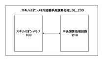
- FIG. 16 shows an example of the configuration of the skyrmion memory 600 according to comparative example 4; FIG. It is a schematic diagram which shows the structural example of central processing processing LSI_200 mounted with skyrmion memory.
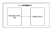
- FIG. 3 is a schematic view showing a configuration example of a data processing device 300.
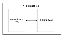
- FIG. 6 is a schematic view showing a configuration example of a data recording device 400.
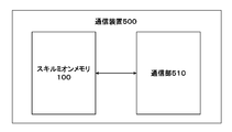
- FIG. 16 is a schematic view showing a configuration example of the communication device 500.
- a chiral magnetic material is an example of a magnetic material that can form skyrmions.
- the chiral magnetic material is a magnetic material in which the arrangement of magnetic moment when no external magnetic field is applied becomes a magnetically ordered phase (helical magnetic phase) rotating in a spiral on the traveling direction of the magnetic moment.
- the chiral magnetic material becomes a ferromagnetic phase through a crystal phase in which skirmions are arranged in a lattice.
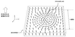
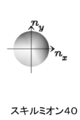
- FIG. 1 is a schematic view showing an example of skirmion 40 which is a nanoscale magnetic structure in magnetic thin film 11.
- each arrow indicates the direction of the magnetic moment in the skyrmion 40.
- the x axis and the y axis are axes orthogonal to each other, and the z axis is an axis orthogonal to the xy plane.
- the magnetic thin film 11 has a plane parallel to the xy plane.
- the magnetic moment directed in any direction in the magnetic thin film 11 constitutes the skirmion 40.
- the direction of the magnetic field applied to the magnetic thin film 11 is the positive z-direction.
- the magnetic moment of the outermost periphery of the skyrmion 40 of this example is directed to the plus z direction.
- the outermost circumference refers to the circumference of the magnetic moment directed in the same direction as the external magnetic field shown in FIG.
- the magnetic moment is arranged so as to spirally rotate from the outermost periphery toward the inner side. Furthermore, the direction of the magnetic moment gradually changes from the plus z direction to the minus z direction toward the center of the vortex as the spiral rotation is performed. Skirmion 40 is a nanoscale magnetic structure having a spiral structure of magnetic moment.
- the magnetic moments constituting the skyrmion 40 consist of the same magnetic moment in the z direction. That is, the skyrmion 40 has a magnetic structure consisting of magnetic moments in the same direction from the front surface to the back surface in the depth direction (z direction) of the closed path shape magnetic thin film 11.
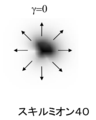
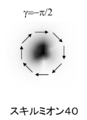
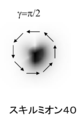
- FIGS. 2A to 2D are schematic diagrams showing skyrmions 40 with different helicity ⁇ (ie, the twisting of the magnetic moment).
- ⁇ the number of skill mions
- FIG. 2E shows how to obtain the coordinates of the magnetic moment (right hand system). Since the right-handed system is used, the n z -axis is taken from the back to the front of the drawing with respect to the n x -axis and the n y -axis. Moreover, the relationship between the density and the direction of the magnetic moment is shown in FIG. 2E.
- the skyrmion number Nsk characterizes skyrmion 40, which is a nanoscale magnetic structure having a spiral structure.
- the following [Equation 1] and [Equation 2] express the number of skill mions Nsk.
- the polar angle ⁇ (r) between the magnetic moment and the z-axis is a continuous function of the distance r from the center of the skyrmion 40.
- the polar angle ⁇ (r) varies from ⁇ to zero or from zero to ⁇ when r is varied from 0 to ⁇ .
- the vector quantity n (r) represents the direction of the magnetic moment of the skyrmion 40 at the position r.
- FIG. 2A to FIG. 2D are schematic diagrams showing skyrmions 40 with different helicity ⁇ .
- FIG. 2E shows how to obtain the coordinates of the magnetic moment (right hand system). Since the right-handed system is used, the n z -axis is taken from the back to the front of the drawing with respect to the n x -axis and the n y -axis. Moreover, the relationship between the density and the direction of the magnetic moment is shown in FIG. 2E.
- FIGS. 2A to 2D the shading indicates the direction of the magnetic moment.
- Each arrow in FIGS. 2A to 2D indicates a magnetic moment separated from the center of the skyrmion 40 by a predetermined distance.
- the magnetic structure shown in FIGS. 2A to 2D is in a state of defining a skyrmion 40.
- the lightest and darkest region indicates the magnetic moment in the direction from the back to the front of the paper.
- the magnetic moment is shown in white.
- the area with the highest density represents the magnetic moment in the direction from the front of the paper to the back.
- each magnetic moment of FIG. 2A 0
- the direction of each magnetic moment in FIG. 2C ⁇ 90 degrees for each magnetic moment in FIG. 2A (90 degrees clockwise) It is the direction of rotation.
- FIGS. 2A-2D appear different but are topologically identical magnetic structures. Skirmions 40 having the structures of FIGS. 2A to 2D are present stably once generated, and function as carriers for transmitting information in the magnetic thin film 11 to which an external magnetic field is applied.
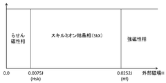
- FIG. 3 is a phase diagram showing the magnetic field dependency of the magnetic substance magnetic phase.
- the chiral magnetic material is a magnetic thin film which changes from a chiral magnetic phase to a skyrmion crystal phase (SkX) by a magnetic field strength Hsk, and changes from a skyrmion crystal phase (SkX) to a ferromagnetic phase at a high magnetic field strength Hf.
- a plurality of skyrmions 40 are aligned in a close-packed structure and occur in the xy plane.
- a is the lattice constant of the magnetic thin film 11
- D is the magnitude of the Jaroshinski-Moriya interaction, and is a physical constant inherent to the substance. Therefore, the skyrmion diameter ⁇ is a substance specific constant.
- the skyrmion diameter ⁇ is, for example, 70 nm for FeGe and 18 nm for MnSi.
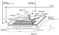
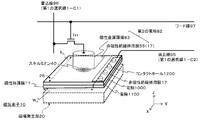
- FIG. 4 shows an example of the configuration of the magnetic element 10 according to the first embodiment.
- the magnetic element 10 shown in FIG. 4 enables generation and erasure of one skyrmion 40 by pulse current.
- the presence or absence of the skyrmion 40 at a predetermined position of the magnetic thin film 11 corresponds to 1-bit information.
- the magnetic element 10 stores (stores) information using the skill muon 40.
- the magnetic element 10 of this example includes a magnetic thin film 11, an upstream electrode 12, a downstream electrode 14, a detection element 15, an erase line 95, a write line 96, a word line 97, a bit line 94, and a transistor Tr1.
- the transistor Tr1 is an example of a transistor portion for selecting the skirmion generating portion having the magnetic thin film 11, the upstream side electrode 12 and the downstream side electrode 14, the erasing portion or the detection element 15. Further, a magnetic field generating unit 20 provided outside the magnetic element 10 which is not the configuration of the magnetic element 10 is shown by a broken line.
- FIG. 4 shows (x, y, z) coordinates.
- the upstream electrode 12 is connected to one end of the magnetic thin film 11.
- the upstream electrode 12 is connected in the spreading direction of the magnetic thin film 11.
- the spreading direction of the magnetic thin film 11 refers to a direction parallel to the xy plane.
- the upstream electrode 12 may be laminated on the end of the magnetic thin film 11.
- the upstream electrode 12 may have a thin layer shape. Further, the upstream electrode 12 may have the same thickness as the magnetic thin film 11.
- the upstream electrode 12 is connected to the write line 96.
- the upstream electrode 12 is made of a conductive nonmagnetic thin film metal such as Cu, W, Ti, TiN, Al, Pt, Au or the like.
- the write line 96 is an example of the first selection line 1-A1.
- the downstream electrode 14 is separated from the upstream electrode 12 and connected to the magnetic thin film 11.
- the downstream electrode 14 in this example is connected to the other end of the magnetic thin film 11 facing the upstream electrode 12.
- the downstream electrode 14 may be connected in the spreading direction of the magnetic thin film 11.
- the downstream electrode 14 may be laminated on the end of the magnetic thin film 11.
- the upstream side electrode 12 and the downstream side electrode 14 are disposed so that a current in a direction substantially parallel to the xy plane flows to the magnetic thin film 11 when a voltage is applied.
- the downstream electrode 14 is connected to the erase line 95.
- the downstream electrode 14 is made of a conductive nonmagnetic thin film metal such as Cu, W, Ti, TiN, Al, Pt, Au or the like.
- the erase line 95 is an example of the first select line 1-A2.
- the magnetic thin film 11 develops at least a skirmion crystal phase and a ferromagnetic phase according to the applied magnetic field.
- the magnetic substance having the skirmion crystal phase and the ferromagnetic phase is a necessary condition that the skirmion 40 can be generated on the magnetic thin film 11.
- the magnetic thin film 11 is a chiral magnetic material, and is formed of FeGe or MnSi having a B20 structure, or CoZn or CoZnMn having a ⁇ Mn structure.
- the magnetic thin film 11 may have a laminated structure of magnetic and nonmagnetic materials.
- a magnetic thin film having a laminated thin film structure of a magnetic thin film and a nonmagnetic thin film is a laminated magnetic thin film in which the magnetic moment of the magnetic thin film is modulated by the spin-orbit interaction of the nonmagnetic thin film.
- the magnetic thin film 11 can be formed on a magnetic thin film formed using an MBE (Molecular Beam Epitaxy) apparatus, a sputtering apparatus, or the like using an exposure apparatus, an etching apparatus, a CMP (Chemical Mechanical Planarization) method.
- the magnetic thin film 11 has a thin film shape.
- the magnetic thin film 11 has a substantially rectangular shape with a width Wm and a length Hm on the thin film plane.
- the width Wm of the magnetic thin film 11 is 3 ⁇ > Wm ⁇ ⁇ where ⁇ is the skyrmion diameter, and the length Hm of the magnetic thin film 11 is 2 ⁇ > Wm ⁇ ⁇ .
- the magnetic thin film 11 has a recess at the end portion between the upstream electrode and the downstream electrode.
- the magnetic thin film 11 may be surrounded by a nonmagnetic insulating material or the like generally used in the semiconductor process.
- a nonmagnetic insulator thin film is provided between the magnetic thin film 11 and the magnetic thin film 11 of the adjacent magnetic element 10.
- the thickness of the magnetic thin film 11 may be, for example, about 10 times or less the diameter ⁇ of the skirmion 40.
- the transistor Tr1 is provided between the downstream electrode 14 and the erase line 95.
- the transistor Tr1 is a field effect transistor (FET).
- the gate terminal of the transistor Tr1 is connected to the word line 97.
- the transistor Tr1 prevents a leak current from flowing through the magnetic element 10 when the corresponding magnetic element 10 is not selected. As a result, it is possible to prevent erroneous writing or erroneous erasing on the magnetic element 10 not to be written. Furthermore, since the leak current can be shut off, power consumption can be reduced. Furthermore, the transistor Tr1 also serves to select the detection element 15.
- the transistor Tr1 is provided between the downstream side electrode 14 and the erase line 95 to enable data reading of the selected magnetic element 10.
- the transistor Tr1 between the upstream electrode 12 and the write line 96.
- the gate terminal of the transistor Tr1 is connected to the word line 97.
- the transistor Tr1 prevents a leak current from flowing through the magnetic element 10 when the corresponding magnetic element 10 is not selected. Also, the transistor Tr1 has a role of selecting the detection element 15, as described above.
- the transistor Tr 2 between the magnetic metal thin film 152 which is the magnetic metal of the detection element 15 and the bit line 94.
- the resistance value between the detection element 15 and the downstream electrode 14 is high.
- detecting the resistance between the magnetic metal thin film 152 of the detection element 15 and the upstream electrode 12 makes it easier to read out the change in the resistance of the detection element 15 due to the presence or absence of skirmion.
- the gate terminal of the transistor Tr2 is connected to the word line 97. A current during generation and generation of the skirmion 40 uses the transistor Tr1, and a detection of the skirmion 40 uses the transistor Tr2. In this case, two transistors are required as the magnetic element.
- the upstream electrode 12 and the downstream electrode 14 either the direction from the upstream electrode 12 to the downstream electrode 14 or the direction from the downstream electrode 14 to the upstream electrode 12 is selected to A pulse current is applied to 11.
- the magnetic element 10 applies a pulse current to the magnetic thin film 11 in the direction from the upstream electrode 12 to the downstream electrode 14 when skirmion 40 is generated in the magnetic thin film 11.
- the pulse electron flow flowing in the magnetic thin film 11 is indicated by the black line arrow.
- the electron current flows in the direction opposite to the current direction.
- the magnetic element 10 when erasing the skyrmions 40 present in the magnetic thin film 11, applies a pulse current to the magnetic thin film 11 in the direction from the downstream electrode 14 toward the upstream electrode 12.
- the magnetic thin film 11 has a recess 16 at the end 18.
- the end portion 18 in this example is an end portion of the end portion of the magnetic thin film 11 that is sandwiched by the upstream side electrode 12 and the downstream side electrode 14.
- the end 18 is an upper or lower end of the magnetic thin film 11 when the upstream electrode 12 is disposed on the right side and the downstream electrode 14 is disposed on the left.
- the recess 16 is provided at an end 18 so as to be separated from both the upstream electrode 12 and the downstream electrode 14.
- the end of the recess 16 on the downstream electrode 14 side extends to the end of the magnetic thin film 11 on the downstream electrode 14 side.
- the magnetic element 10 comprises an L-shaped magnetic thin film 11.
- a nonmagnetic thin film may be provided inside the recess 16.
- the magnetic element 10 uses one skyrmion 40 generated by current as an information storage medium.
- One skyrmion 40 can be generated from the recess 16 of the magnetic thin film 11 by the pulsed electron current.
- the corner portion facing the upstream electrode 12 is referred to as a first corner portion 24.
- a pulse current is caused to flow from the upstream electrode 12 to the downstream electrode 14. That is, a pulsed electron current is applied from the downstream electrode 14.
- skirmions 40 are generated near the first corner 24.
- the recess 16 may have a side parallel to the upstream electrode 12 or a side parallel to the downstream electrode 14.
- the first corner 24 may be an end of a side parallel to the upstream electrode 12.
- the recess 16 in this example has a rectangular shape.
- the shape of the recess 16 is not limited to a square.
- the shape of the recess 16 may be polygonal.
- each side of the recessed part 16 does not need to be a straight line.
- the first corner 24 of the recess 16 may be rounded.
- the magnetic thin film 11 becomes a ferromagnetic phase by the magnetic field generator 20. For this reason, the magnetic moment in the magnetic thin film 11 is in the same direction as the magnetic field H. However, the magnetic moment at the end of the magnetic thin film 11 is not directed in the same direction as the magnetic field H, and has a tilt relative to the magnetic field H. In particular, in the vicinity of the first corner 24 of the recess 16, the inclination of the magnetic moment changes continuously. For this reason, the first corner 24 of the magnetic thin film 11 is more susceptible to skirmion 40 than the other regions, and the skirmion 40 can be generated by a predetermined pulsed electron current.
- the first corner 24 is formed to have a predetermined internal angle.
- the internal angle of the first corner 24 is 180 ° or more.
- the internal angle of the first corner 24 in the recess 16 refers to the angle on the magnetic thin film 11 side of the first corner 24.
- the internal angle of the first corner 24 adjacent to the upstream electrode 12 is 270 °.
- the inner angle of the first corner 24 be 270 ° in the generation of the skirmion 40.
- the skirmion 40 can be erased by flowing a pulse current from the downstream electrode 14 toward the upstream electrode 12 to the magnetic thin film 11.
- the direction of the pulsed electron current is opposite to that in FIG.
- the skirmion 40 is driven to the first corner 24 and erased.
- the skirmion 40 can be chased at the first corner 24 and erased.
- the detection element 15 is a tunnel magnetoresistive element (TMR element).
- TMR element tunnel magnetoresistive element
- the detection element 15 of this example is provided between the upstream electrode 12 and the first corner 24 of the recess 16.
- the detection element 15 has a laminated structure of a nonmagnetic insulator thin film 151 formed on the magnetic thin film 11 and a magnetic metal thin film 152 made of metal formed on the nonmagnetic insulator thin film 151.
- the detection element 15 measures the value of the resistance of the nonmagnetic insulator thin film 151 between the magnetic metal thin film 152 and the magnetic thin film 11.
- the resistance value of the nonmagnetic insulator thin film 151 shows the maximum value, and when the Skirmion 40 does not exist, the resistance value of the nonmagnetic insulator thin film 151 shows the minimum value. Show.
- the high resistance (H) state and the low resistance (L) state of the detection element 15 correspond to the presence or absence of the skyrmion 40, and correspond to the information "1" and "0" stored by the memory cell.
- the detection element 15 is a tunnel magnetoresistive (TMR) element.
- TMR tunnel magnetoresistive
- the detection element 15 utilizes the effect that the resistance value of the insulator thin film sandwiched between the magnetic metal thin films depends on the state of the magnetic moment of both magnetic thin films.
- the magnetic metal thin film 152 constituting the detection element 15 has a magnetic moment in the z direction due to the magnetic field from the magnetic field generation unit 20.
- the magnetic moment of the magnetic thin film 11 is a vortex.
- the quantum effect on the tunnel electron current flowing in the nonmagnetic insulator thin film 151 is reduced. As a result, the tunnel current flowing through the nonmagnetic insulator thin film 151 is reduced.
- the resistance value of the nonmagnetic insulator thin film 151 shows the maximum value.
- a magnetic moment M in the z direction identical to the magnetic field H of the magnetic field generation unit 20 is generated in the magnetic thin film 11.
- the magnetic metal thin film 152 also generates a magnetic moment M in the z direction, which is the same as the magnetic field H of the magnetic field generation unit 20.
- a tunnel current flows more to the nonmagnetic insulator thin film 151 between the magnetic metal thin film 152 and the magnetic thin film 11 due to the quantum effect. That is, the resistance value of the nonmagnetic insulator thin film 151 exhibits the minimum value.
- the resistance value of the nonmagnetic insulator thin film 151 is higher in the presence of the skirmion 40 than in the absence of the skirmion 40. By detecting this resistance value, it is possible to detect the presence or absence of the skirmion 40 and read the information stored in the magnetic element 10.
- the magnetic metal thin film is a magnetic metal thin film such as Co, Ni, Fe or the like, or a laminated magnetic metal thin film formed of these magnetic metal thin films.
- the bit line 94 is connected to the magnetic element 10 and applies a constant current to generate a voltage according to the presence or absence of the skirmion 40 of the corresponding magnetic element 10. That is, the bit line 94 functions as a skillion detection line. Bit line 94 is an example of a second select line.
- the detection element 15 of this example was provided in contact with the top surface of the magnetic thin film 11.
- the detection element 15 may be a detection element formed so as to sandwich the nonmagnetic insulator thin film 151 between the magnetic thin film and the soft magnetic thin film.
- the direction of the magnetic moment of the soft magnetic thin film is the direction of the magnetic moment corresponding to the magnetic structure of the magnetic thin film 11. If the detection element of this structure is formed directly on the magnetic thin film 11, skirmion 40 can be detected with high sensitivity.
- the transistor Tr2 for selecting the detection element 15 is essential.
- the transistor Tr1 can not double as the selection of the detection element 15.
- FIG. 4 shows a magnetic field generation unit 20 which is a component of the skillion memory 100 according to the first embodiment.
- FIG. 4 shows (x, y, z) coordinates.
- the magnetic field generation unit 20 applies a magnetic field H to the magnetic thin film 11.
- the magnetic field generation unit 20 of this example turns the magnetic thin film 11 into a ferromagnetic phase.
- the magnetic field generation unit 20 applies a magnetic field H substantially perpendicular to the surface of the thin film magnetic thin film 11 to the magnetic thin film 11.
- the magnetic thin film 11 has a surface (one surface) parallel to the xy plane, and the magnetic field generating unit 20 generates a magnetic field H in the positive z direction as indicated by the arrow in the magnetic field generating unit 20.
- the magnetic field generating unit 20 may be provided to face the back surface of the magnetic thin film 11.
- the magnetic field generation unit 20 may be separated from or in contact with the magnetic thin film 11.
- the magnetic field generator 20 is preferably separated from the magnetic thin film 11.
- the size of the area of the magnetic field generation unit 20 facing the magnetic thin film 11 may not be the same as that of the magnetic thin film 11.
- the magnetic field generation unit 20 may also be used as a magnetic field generation unit 20 for another magnetic thin film 11.
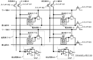
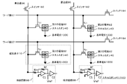
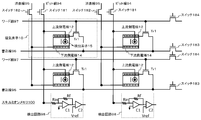
- FIG. 5A shows an example of the configuration of the skill meon memory 100 according to the first embodiment.
- the skyrmion memory 100 of this example includes the magnetic element 10 illustrated in FIG.
- the magnetic element 10 comprises an L-shaped magnetic thin film 11.
- An upstream electrode 12 and a downstream electrode 14 are provided.
- a detection element 15 is provided.
- a transistor Tr1 is provided between the downstream electrode 14 and the erase line 95.
- the present magnetic element 10 is characterized in that it comprises only one transistor.
- the transistor Tr1 is a transistor for selecting the L-shaped magnetic thin film and for selecting the detection element 15.
- the skyrmion memory 100 of this example includes a plurality of the magnetic elements 10 shown in FIG. 3 in a matrix.
- FIG. 5A shows only some of the columns and rows of the matrix.
- the skyrmion memory 100 includes a plurality of magnetic elements 10, a plurality of bit lines 94, a plurality of erase lines 95, a plurality of write lines 96, a plurality of word lines 97, a plurality of switches 181, a plurality of switches 182, and a plurality of switches 183, a plurality of switches 184 and a plurality of detection circuits 98.
- the write line 96 is connected to the magnetic element 10 and supplies a generation current for generating the skirmions 40 of the corresponding magnetic element 10. That is, the write line 96 functions as a skillion generation line.
- the erase line 95 is connected to the magnetic elements 10, and supplies an erasing current for erasing the skyrmions 40 to the corresponding magnetic elements 10. That is, the erase line 95 functions as a skirmion erase line.
- the bit line 94 is connected to the magnetic element 10 and applies a constant current to generate a voltage according to the presence or absence of the skirmion 40 of the corresponding magnetic element 10. That is, the bit line 94 functions as a skillion detection line.
- the word line 97 connects to the magnetic element 10 and selects the magnetic element 10 that generates, erases and detects skirmions 40.
- the word line 97 in this example is connected to the gate terminal of the transistor Tr1.
- a switch 181 is provided for each bit line 94.
- a switch 182 is provided for each erase line 95.
- a switch 183 is provided for each write line 96.
- a switch 184 is provided on each word line 97.
- the switches 181, 182, 183, and 184 are FETs.
- Erase line 95 and write line 96 are connected to an external pulse current source via respective switches.
- the external pulse current sources may be a common pulse current source.
- the external pulse current source may be provided for each erase line 95 or may be provided commonly to the plurality of erase lines 95.
- the detection circuit 98 is connected to the bit line 94 and detects the voltage of the bit line 94.
- the detection circuit 98 may be provided for each bit line 94, or may be provided commonly for the plurality of bit lines 94.
- the detection circuit 98 of this example amplifies the voltage of the bit line 94 to detect the presence or absence of the skirmion 40.
- the detection circuit 98 includes an input resistor Rin, a feedback resistor Rf, an amplifier circuit C1 and a voltage comparison circuit C2.
- the voltage of the bit line 94 is amplified by the ratio of the input resistance Rin to the feedback resistance Rf.
- the differential voltage is amplified by inputting both the output voltage of the amplification circuit C1 and the reference voltage Vref to the voltage comparison circuit C2.
- the voltage comparison circuit C2 outputs “1” when the output voltage of the amplification circuit C1 is larger than the reference voltage Vref.
- the voltage comparison circuit C2 outputs “0” when the output voltage of the amplification circuit C1 is smaller than the reference voltage Vref.
- the upstream electrode 12 of the magnetic element 10 is connected to the corresponding write line 96.
- the downstream electrode 14 is connected to the corresponding erase line 95.
- the detection element 15 is connected to the corresponding bit line 94.
- the transistor Tr1 is provided to select the magnetic thin film 11.
- the transistor Tr1 of this example is provided between the upstream electrode 12 and the write line 96.
- the gate terminal of the transistor Tr1 is connected to the word line 97.
- the transistor Tr1 prevents a leak current from flowing through the magnetic element 10 when the corresponding magnetic element 10 is not selected.
- the leakage current generates the skill ions 40 in the non-selected magnetic elements 10 to cause erroneous writing.
- the leakage current erases the skyrmions 40 of the non-selected magnetic element 10 to cause erroneous erasure.
- the skyrmion memory 100 of this example can shut off the leak current through the magnetic element 10, and prevents erroneous writing and erroneous erasing.
- a transistor Tr1 is provided between at least one of the upstream electrode 12 and the write line 96 or between the downstream electrode 14 and the erase line 95.
- FIG. 5A shows the case where a transistor Tr1 is provided between the downstream electrode 14 and
- the transistor Tr1 between the downstream electrode 14 and the erase line 95, it is possible to select the detection element 15 of the magnetic element 10 from which data is to be read.
- the resistance value between the detection element 15 of the non-selected magnetic element 10 and the erase line 95 can be made infinite by the transistor Tr1.
- the corresponding bit line 94 of the magnetic element 10 for which data is to be read is selected, and a constant current is supplied to the bit line 94.
- the voltage of the selected bit line 94 is determined by the resistance value indicated by the detection element 15 of the magnetic element 10 in which the transistor Tr1 is turned on.
- the resistance value of all the other magnetic elements 10 connected to the selected bit line 94 is infinite because the transistor Tr1 is off.
- the voltage of the selected bit line 94 is a voltage due to the resistance value of only the TMR element of the selected magnetic element 10.
- FIG. 5B illustrates an example of the configuration of the skill meon memory 100 according to the first embodiment.
- the skyrmion memory 100 of this example is the case where the transistor Tr 2 is provided between the bit line 94 and the detection element 15.
- the transistor Tr1 is necessary to select the magnetic element 10.
- the transistor Tr1 and the transistor Tr2 are an example of a transistor unit.
- the transistor Tr1 is provided to select the magnetic thin film 11.
- the transistor Tr1 of this example is provided between the downstream electrode 14 and the erase line 95.
- the gate terminal of the transistor Tr1 is connected to the word line 97.
- the transistor Tr1 prevents a leak current from flowing through the magnetic element 10 when the corresponding magnetic element 10 is not selected.
- the skyrmion memory 100 of this example can shut off the leak current through the magnetic element 10.
- the skyrmion memory 100 of this example can prevent erroneous writing and erasing of the skyrmion 40 and, at the same time, can suppress an increase in power consumption.
- the transistor Tr2 is provided to directly select the detection element 15.
- the transistor Tr1 of this circuit can not select the detection element 15.
- the transistor Tr 2 is provided between the detection element 15 and the bit line 94.
- the gate terminal of the transistor Tr2 is connected to the word line 97.
- the transistor Tr1 for selecting the magnetic thin film 11 is provided between at least one of the upstream electrode 12 and the write line 96 or between the downstream electrode 14 and the erase line 95. .
- the leak current of the skill-ion memory 100 can be shut off, and erroneous writing and erroneous erasing can be prevented.
- the detection element 15 can be further selected.
- the magnetic element 10 is a single transistor Tr 1, which can shut off the leak current and prevent the erroneous writing, and can generate, erase and detect the skirmion 40.
- the switch 183 of the upper write line 96 is turned on.
- the switch 182 of the left erase line 95 is turned on.
- the switch 184 of the upper word line 97 is turned on.
- a pulse current for skirmion generation is applied to the upper write line 96.
- the pulse current is applied only to the upper left magnetic element 10.
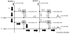
- FIG. 6 shows the configuration of the skill meon memory 600 according to the first comparative example.
- the skyrmion memory 600 of this example does not have the transistor Tr1.
- the skirmion memory 600 of the present example causes the generated current Ig to flow to the upper left magnetic element 10 by turning on the switch 182 and the switch 184.
- the generated current Ig is indicated by a solid arrow.
- the leakage current IL is indicated by an open arrow. Since the magnetic thin film 11 is a metal material, the leak current IL has a large value.
- the leak current IL causes erroneous writing, erroneous erasure, and increased power consumption of the skirmion 40.
- the current direction of the leakage current IL of the magnetic element 10 at the upper right and lower left is the current in the generation direction of the skyrmion 40, so the skyrmion 40 is generated in the magnetic element 10 at the upper right Resulting in. That is, erroneous writing occurs.
- the skyrmion 40 is present when the skyrmion 40 exists in the lower right magnetic element 10. Erase the That is, erroneous erasure occurs. Also, the skyrmion memory 600 has a large number of magnetic elements 10 in a matrix. Since the leak current IL is generated through each of the magnetic elements 10, the entire skillion memory 600 consumes a large amount of power.
- the transistor Tr1 according to the first embodiment is provided in at least one of between the upstream electrode 12 and the write line 96 or between the downstream electrode 14 and the erase line 95. That is, while the transistor Tr1 of this example is provided for each of the magnetic thin films 11 that generate one skirmion 40, the switches 182 and 184 are provided for two or more of the magnetic thin films 11. There is a big difference in Thereby, the skyrmion memory 100 of the first embodiment can shut off the leak current through the magnetic element 10. As described above, by blocking the leakage current through the magnetic element 10, the skyrmion memory 100 according to the present specification can prevent erroneous writing and prevent erroneous erasure, and has excellent performance with low power consumption. Indicates Furthermore, the transistor Tr1 functions as a transistor that selects the detection element 15. As a result, memory cells can be made smaller and higher density can be achieved.
- FIG. 7 is a schematic view showing the magnetic element 10 according to the second embodiment.
- the magnetic element 10 of this example enables the generation of the skirmion 40.
- the magnetic element 10 stores bit information using the skyrmion 40.
- the presence or absence of the skyrmion 40 in the magnetic thin film 11 corresponds to 1-bit information.
- the magnetic element 10 of this example includes the magnetic thin film 11, the current path 13, the detection element 15, the nonmagnetic insulator thin film 17, the electrode 1000, the electrode 1100, the contact hole 1200, the write line 96, the erase line 95, and the word line 97. And a transistor Tr1.
- the magnetic field generation unit 20 indicated by a broken line is not the configuration of the magnetic element 10.
- the magnetic thin film 11 may be surrounded by an insulating silicon oxide material or the like generally used in a semiconductor process. In addition, the magnetic thin film 11 surrounds all directions with a nonmagnetic material.
- the current path 13 surrounds a region including the end of the magnetic thin film 11 on one surface of the magnetic thin film 11.
- the current path 13 may be electrically isolated from the magnetic thin film 11 by using a nonmagnetic insulator thin film 17 or the like of a nonmagnetic material.
- the current path 13 in this example is a current circuit formed in a U-shape.
- the U-shape may be a shape including not only a shape having rounded corners but also a right angle as in this example.
- the current path 13 may not form a closed region in the xy plane.
- the combination of the current path 13 and the end 18 may form a closed region on the surface of the magnetic thin film 11. In the current path 13, current flows in the direction indicated by the arrow C.
- the current path 13 is formed of a nonmagnetic metal material such as Cu, W, Ti, Al, Pt, Au, TiN, AlSi.
- a U-shaped region where the region surrounded by the current path 13 includes the end of the magnetic thin film 11 is particularly referred to as an end region A.
- the current path 13 in this example crosses the end of the magnetic thin film 11 at least once from the nonmagnetic thin film side to the magnetic thin film 11 in the xy plane, and from the magnetic thin film 11 to the nonmagnetic thin film It has a continuous conducting path which traverses at least once on the side.
- the current path 13 surrounds a region including the end of the magnetic thin film 11.
- the magnetic field strength in the end region A is set to Ha.
- the current C flowing through the current path 13 generates a magnetic field (-Hc) from the front surface to the back surface of the magnetic thin film 11 in the U-shaped region surrounded by the current path 13.
- the direction of this magnetic field is negative with respect to the z direction. Since the direction of the magnetic field induced by the current flowing through the current path 13 is opposite to the direction (plus direction of the z axis) of the uniform magnetic field H from the magnetic field generation unit 20, the magnetic thin film A weak magnetic field Ha is generated from the back surface of the surface 11 to the surface direction.
- Equation 3) Ha H-Hc
- the skirmion 40 can be generated in the end area A.
- the current path 13 may have a laminated structure of a nonmagnetic insulator thin film formed on the magnetic thin film 11 and a nonmagnetic metal thin film formed on the nonmagnetic insulator thin film.
- the nonmagnetic insulator thin film included in the current path 13 may be the same nonmagnetic insulator thin film as the nonmagnetic insulator thin film 151 included in the detection element 15.
- the nonmagnetic insulator thin film included in the current path 13 and the nonmagnetic insulator thin film 151 have the same process, material, and / or thickness.
- One end of the current path 13 is the current path upstream end portion 131 connected to the write line 96.
- the write line 96 is an example of the first select line 1-B1.
- the other end is the current path downstream end 132 connected to the erase line 95.
- the erase line 95 is an example of the first select line 1-B2.
- the current path upstream end portion 131 may be electrically connected to the magnetic thin film 11.
- the current path upstream end portion 131 is electrically connected to the electrode 1100 and electrically connected to the electrode 1000 via the contact hole 1200.
- the electrodes 1000 and 1100 are made of a conductive nonmagnetic metal thin film such as Cu, W, Ti, TiN, Al, Pt, Au or the like.
- the transistor Tr 1 is provided between the current path upstream end 131 and the write line 96 or between the current path downstream end 132 and the erase line 95.
- the gate terminal of the transistor Tr1 is connected to the word line 97.
- the transistor Tr1 prevents a leak current from flowing through the magnetic element 10 when the corresponding magnetic element 10 is not selected. Thereby, the skyrmion memory 100 of this example can shut off the leak current through the magnetic element 10. That is, the transistor Tr1 is provided in at least one of between the current path upstream end 131 and the write line 96 or between the current path downstream end 132 and the erase line 95.
- the detection element 15 is a tunnel magnetoresistive element (TMR element).
- TMR element tunnel magnetoresistive element
- the detection element 15 is a detection element having the same laminated structure as that of the first embodiment.
- the detection element 15 of this example is provided between the U-shaped current path 13 and the end 18 of the magnetic thin film 11.
- the detection function of the skill muon 40 is the same as the detection function in the first embodiment.
- the magnetic thin film 11 is used as the other electrode.
- an electrode 1000 of nonmagnetic metal is provided at the end of the magnetic thin film 11.
- the electrode 1000 may be provided on the spread portion of the magnetic thin film. It may be laminated on the end of the magnetic thin film 11.
- a contact hole 1200 may be provided for electrical connection to the electrode 1000, and an electrode 1100 may be provided on the upper layer.
- the bit line 94 is connected to the magnetic element 10 and applies a constant current to generate a voltage according to the presence or absence of the skirmion 40 of the corresponding magnetic element 10. That is, the bit line 94 functions as a skillion detection line. Bit line 94 is an example of a second select line.
- the transistor Tr1 can be selected between the current path upstream end portion 131 and the write line 96 to select the detection element 15 of the magnetic element 10 from which data is to be read.
- the resistance value between the detection element 15 of the non-selected magnetic element 10 and the write line 96 can be made infinite by the transistor Tr1. As a result, only the resistance value of the detection element 15 of the selected magnetic element 10 can be read.
- FIG. 8 shows an example of the configuration of the skill-ion memory 100 according to the second embodiment.
- the skyrmion memory 100 of this example is different from the skyrmion memory 100 according to the first embodiment in that a magnetic element 10 that generates and erases skyrmions 40 using a U-shaped current path 13 is used. That is, the magnetic element 10 of this example generates and cancels skyrmions 40 by the current-induced local magnetic field.
- the skyrmion memory 100 of the present example is provided with a U-shaped current path 13 including the end of the magnetic thin film. In the case of a current path having a shape that does not include the magnetic thin film end, skirmion 40 can not be generated.
- the skyrmion memory 100 of this example includes a plurality of magnetic elements 10 shown in FIG. 7 in a matrix. FIG. 8 shows only some of the plurality of columns and rows of the matrix.
- the skyrmion memory 100 includes a plurality of magnetic elements 10, a plurality of bit lines 94, a plurality of erase lines 95, a plurality of write lines 96, a plurality of word lines 97, a plurality of switches 181, a plurality of switches 182, and a plurality of switches 183, a plurality of switches 184 and a plurality of detection circuits 98.
- the write line 96 is connected to the magnetic element 10 and supplies a generation current for generating the skirmions 40 of the corresponding magnetic element 10. That is, the write line 96 functions as a skillion generation line.
- the erase line 95 is connected to the magnetic elements 10, and supplies an erasing current for erasing the skyrmions 40 to the corresponding magnetic elements 10. That is, the erase line 95 functions as a skirmion erase line.
- the word line 97 connects to the magnetic element 10 and selects the magnetic element 10 that generates, erases and detects skirmions 40.
- the word line 97 in this example is connected to the gate terminal of the transistor Tr1.
- a switch 181 is provided for each bit line 94.
- a switch 182 is provided for each erase line 95.
- a switch 183 is provided for each write line 96.
- a switch 184 is provided on each word line 97.
- the switches 181, 182, 183, and 184 are FETs.
- Erase line 95 and write line 96 are connected to an external pulse current source via respective switches.
- the external pulse current sources may be a common pulse current source.
- the external pulse current source may be provided for each erase line 95 or may be provided commonly to the plurality of erase lines 95.
- the detection circuit 98 is connected to the bit line 94 and detects the voltage of the bit line 94.
- the detection circuit 98 may be provided for each bit line 94, or may be provided commonly for the plurality of bit lines 94.
- the detection circuit 98 of this example amplifies the voltage of the bit line 94 to detect the presence or absence of the skirmion 40.
- the detection circuit 98 includes an input resistor Rin, a feedback resistor Rf, an amplifier circuit C1 and a voltage comparison circuit C2.
- the voltage of the bit line 94 is amplified by the ratio of the input resistance Rin to the feedback resistance Rf.
- the differential voltage is amplified by inputting both the output voltage of the amplification circuit C1 and the reference voltage Vref to the voltage comparison circuit C2.
- the voltage comparison circuit C2 outputs “1” when the output voltage of the amplification circuit C1 is larger than the reference voltage Vref.
- the voltage comparison circuit C2 outputs “0” when the output voltage of the amplification circuit C1 is smaller than the reference voltage Vref.
- FIG. 9 shows an example of the configuration of the skill-ion memory 600 according to the second comparative example.
- the skyrmion memory 600 of this example does not have the transistor Tr1.
- the skirmion memory 600 of the present example causes the generated current Ig to flow through the magnetic element 10 by turning on the switch 182 and the switch 183.
- the generated current Ig is indicated by a solid arrow.
- the leakage current IL is indicated by an open arrow. Since the magnetic thin film 11 is a metal material, the leak current IL has a large value.
- the leak current IL is a cause of causing erroneous write, erroneous erase, and increase in power consumption of the skirmion 40 as in the first comparative example.
- the transistor Tr1 according to the second embodiment is provided between the current path upstream end 131 and the write line 96 or between the current path downstream end 132 and the erase line 95. That is, while the transistor Tr1 of this example is provided for each of the magnetic thin films 11 that generate one skirmion 40, the switches 182 and 184 are provided for two or more of the magnetic thin films 11. There is a big difference in Thereby, the skyrmion memory 100 of the second embodiment can shut off the leak current through the magnetic element 10. As described above, the skillion memory 100 according to the present specification can prevent erroneous writing and erroneous erasure of the skillion 40 by blocking the leakage current through the magnetic element 10, and has excellent performance with low power consumption. Have. Furthermore, the transistor Tr1 functions as a transistor that selects the detection element 15. As a result, memory cells can be made smaller and higher density can be achieved.
- FIG. 10 is a schematic view showing an example of the magnetic element 10 according to the third embodiment.
- the magnetic element 10 of this example enables generation of the skyrmions 40 using local heat.
- the magnetic element 10 of this example uses the skyrmion 40 to store bit information.
- the presence or absence of the skyrmion 40 in the magnetic thin film 11 corresponds to 1-bit information.
- the magnetic element 10 of this example includes the magnetic thin film 11, the second electrode 82, the nonmagnetic insulator thin film 17, the electrode 1000, the electrode 1100, the contact hole 1200, the write line 96, the erase line 95, the word line 97, and the transistor. It has Tr1.
- the write line 96 doubles as a bit line which is an example of a second select line.
- the second electrode 82 includes a nonmagnetic insulator thin film 55 provided in contact with the upper portion of the other surface 26 of the magnetic thin film 11 and a magnetic metal thin film 83 provided in contact with the upper portion of the nonmagnetic insulator thin film 55. And a laminated structure thin film.
- the detection element doubles as the second electrode 82.
- the magnetic field generation unit 20 indicated by a broken line is not the configuration of the magnetic element 10.
- the magnetic metal thin film 83 is a cylindrical magnetic metal thin film.
- the circular cross-sectional area of the magnetic metal thin film 83 is the area in contact with the other surface 26 of the magnetic thin film 11, and the radius of the circular cross section of the magnetic metal thin film 83 corresponds to the spot size radius of the local thermal energy.
- a nonmagnetic insulator thin film 55 is formed between the magnetic metal thin film 83 and the magnetic thin film 11.
- the magnetic thin film 11 is a flat plate parallel to the xy plane.
- the magnetic metal thin film 83 is a magnetic metal thin film made of Co, Ni, Fe, or a laminated magnetic metal thin film made of these magnetic metal thin films.
- the magnetic thin film 11 may be connected to a reference terminal set to a reference potential.
- the electrode 1000 is connected to the other end of the magnetic thin film 11.
- the electrode 1000 may be connected in the spreading direction of the magnetic thin film 11. It is connected to the electrode 1100 via the contact hole 1200.
- the electrode 1100 is connected to the reference potential.
- the electrodes 1000 and 1100 are made of a conductive nonmagnetic metal thin film such as Cu, W, Ti, TiN, Al, Pt, Au or the like.
- the Joule heat generated in the nonmagnetic insulator thin film 55 heats the magnetic material thin film 11 when a pulse current flows through the nonmagnetic insulator thin film 55 of the second electrode 82.
- Local heat can be generated in the nonmagnetic insulator thin film 55 by the circular cross-sectional size of the magnetic metal thin film 83.
- the pulsatile heat enables the generation and elimination of skyrmions 40 by controlling the heat energy.
- the second electrode 82 doubles as a detection element.
- the second electrode 82 is a tunnel magnetoresistive element (TMR element).
- the detection element 15 is a detection element having the same laminated structure as that of the first embodiment.
- the detection function of the skill muon 40 is the same as the detection function in the first embodiment.
- the magnetic thin film 11 is used as the other electrode.
- the nonmagnetic metal thin film electrode 1000 is provided at the end of the magnetic thin film 11.
- the electrode 1000 may be provided on the spread portion of the magnetic thin film 11.
- a contact hole 1200 may be provided for electrical connection to the electrode 1000, and an electrode 1100 may be provided on the upper layer.
- the electrode 1000 or the electrode 1100 is connected to the erase line 95.
- the transistor Tr1 is provided between the magnetic metal thin film 83 of the second electrode 82 and the write line 96. It is a major feature of the magnetic element 10 that the write line 96 doubles as a bit line which is an example of a second select line.
- the gate terminal of the transistor Tr1 is connected to the word line 97.
- the transistor Tr1 prevents a leak current from flowing through the magnetic element 10 when the corresponding magnetic element 10 is not selected. Thereby, the skyrmion memory 100 of this example can shut off the leak current through the magnetic element 10. That is, the transistor Tr1 is provided at least one of between the second electrode 82 and the write line 96 or between the magnetic thin film 11 and the erase line 95.
- the write line 96 in this example is an example of the first select line 1-C1.
- the erase line 95 in this example is an example of the first select line 1-C2.
- the transistor Tr1 between the second electrode 82 and the write line 96, the detection element 15 of the magnetic element 10 from which data is to be read can be selected.
- the resistance value of the write line 96 and the erase line 95 of the magnetic element 10 which is connected to the write line 96 but not selected by the transistor Tr1 can be infinite. As a result, only the resistance value of the detection element 15 of the selected magnetic element 10 can be read.
- the second electrode 82 of the generation unit that generates the skirmion 40 can double as the detection element 15.
- write line 96 can double as a bit line, and wiring space can be significantly reduced.
- the area of the magnetic thin film 11 can be reduced.
- the third embodiment can realize a high density memory element.
- FIG. 11 shows an example of the configuration of the skill meon memory 100 according to the third embodiment.
- the skyrmion memory 100 according to the present embodiment is different from the skyrmion memory 100 according to the first and second embodiments in that the magnetic element 10 generates and erases the skyrmion 40 by applying local heat to the magnetic thin film 11. It is different.
- the magnetic element 10 shown in FIG. 10 may be used as the magnetic element 10 of this example.
- the magnetic element 10 of this example is different from the other examples in principle of generating and erasing Squirmion 40, the method of blocking the basic leak current and the method of selecting the detecting element 15 are the first to the second examples. The same as in the case of the second example.
- the magnetic thin film 11 is connected to the reference potential 1300 via the erase line 95.
- the transistor Tr1 is provided between the magnetic element 10 and the write line 96. Also, the transistor Tr1 may be provided between the magnetic element 10 and the erase line 95. Even in this case, the transistor Tr1 can shut off the leakage current of the magnetic element 10. It is also possible to detect the skyrmion 40 of the selected magnetic element.
- the transistor Tr1 is provided between at least one of the second electrode 82 and the write line 96 or between the magnetic thin film 11 and the erase line 95.
- FIG. 12 shows the configuration of the skill-ion memory 600 according to comparative example 3.
- the skyrmion memory 600 of this example does not have the transistor Tr1.
- the skirmion memory 600 of this example causes the generated current Ig to flow through the magnetic element 10 by turning on the switch 182 and the switch 184.
- the generated current Ig is indicated by a solid arrow.
- the leak current IL causes erroneous write, erroneous erase, and increase in power consumption of the skirmion 40 as in the first comparative example.
- erroneous writing and erroneous erasing of the skyrmion 40 occur depending on the magnitude of the leakage current IL.
- the transistor Tr1 according to the third embodiment is provided between the second electrode 82 and the write line 96.
- the skyrmion memory 100 of the first embodiment can shut off the leak current through the magnetic element 10.
- the skillion memory 100 according to the present specification prevents erroneous writing and erroneous erasing, and has excellent performance with low power consumption.
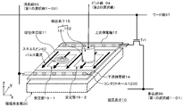
- FIG. 13 is a schematic view showing an example of the magnetic element 10 according to the fourth embodiment.
- the magnetic element 10 of this example enables the transfer of the skirmion 40.
- a configuration example of the magnetic element 10 in which the direction of the current flowing between the upstream side electrode 12 and the downstream side electrode 14 is arranged substantially perpendicular to the direction of transferring the skyrmion 40 is shown as a lateral current arrangement.
- the magnetic element 10 of this example includes the magnetic thin film 11, the upstream electrode 12, the downstream electrode 14, the detection element 15, the stabilizer 19-1, the stabilizer 19-2, the contact hole 1200, the write line 96, the erase line And 95, a bit line 94, a word line 97, and a transistor Tr1.
- the skyrmions 40 in the magnetic thin film 11 can be reduced to stable portions 19-1 (first stable portions) or stable portions 19-2 of the magnetic thin film 11 (first Can be transferred and placed in the second stabilizer).
- a major feature is that the direction of the current flowing between the upstream side electrode 12 and the downstream side electrode 14 is a lateral current arrangement in which the direction of the current is substantially perpendicular to the direction of transferring the skyrmion 40.
- the detection element 15 of this example is provided corresponding to one of the plurality of stabilizing portions 19.
- the presence or absence of skyrmions 40 in the stable portion 19-2 of the magnetic thin film 11 in which the detection element 15 is present corresponds to 1-bit information.
- the magnetic field generation unit 20 indicated by a broken line is not the configuration of the magnetic element 10.
- the magnetic thin film 11 has two stable portions 19.
- the two stable portions 19 are provided in the region of the magnetic thin film 11 sandwiched by the upstream electrode 12 and the downstream electrode 14.
- the magnetic thin film 11 of the present example has a stable portion 19-1 and a stable portion 19-2.
- the stable portion 19 refers to a region where the skyrmions 40 can exist more stably than the other regions of the magnetic thin film 11.
- the stabilizing unit 19 may point to an area where the skirmion 40 stays at that location unless the skirmion 40 is externally powered by, for example, a current or the like.
- the magnetic field strength generated from the magnetic field generation unit 20 can be realized by setting the magnetic field strength weaker than the magnetic field strength around the stable portion 19 as described below.
- the stabilizing unit 19 may indicate an area isolated by any barrier.
- This barrier can be realized by providing the upstream side electrode 12 and the downstream side electrode 14 with a protruding portion that protrudes inside the magnetic thin film 11.
- Each stable portion 19 occupies a predetermined range on the surface of the magnetic thin film 11 parallel to the xy plane.
- the magnetic element 10 can transfer the skirmion 40 between the plurality of stabilizing portions 19 by the transfer current.
- the magnetic field applied to the stable portion 19-1 and the stable portion 19-2 of the magnetic thin film 11 is a magnetic field Ha smaller than the magnetic field strength H applied to the other region of the magnetic thin film 11.
- the magnetic field generation unit 20 is used such that the magnitude of the magnetic moment of the region facing the stable portion 19 is smaller than that of the other regions.
- the upstream electrode 12 is made of nonmagnetic metal connected to the magnetic thin film 11.
- the upstream electrode 12 is connected in the spreading direction of the magnetic thin film 11.
- the spreading direction of the magnetic thin film 11 refers to a direction parallel to the xy plane.
- the upstream electrode 12 may have a thin layer shape. Further, the upstream electrode 12 may have the same thickness as the magnetic thin film 11.
- the downstream electrode 14 is made of nonmagnetic metal separated from the upstream electrode 12 and connected to the magnetic thin film 11.
- the downstream electrode 14 is connected in the spreading direction of the magnetic thin film 11.
- the upstream side electrode 12 and the downstream side electrode 14 are disposed so that a transfer current in a direction substantially parallel to the xy plane flows to the magnetic thin film 11 when a voltage is applied.
- the upstream electrode 12 and the downstream electrode 14 are used to transfer skirmions 40 in the magnetic thin film 11. Note that at least one of the upstream side electrode 12 and the downstream side electrode 14 in the present example also functions as an electrode that causes a current to flow to the detection element 15 that detects the position of the skirmion 40.
- the detection element 15 of this example is a tunnel magnetoresistive element (TMR element).
- TMR element tunnel magnetoresistive element
- the detection element 15 is located in at least one stabilizer.
- the detection element 15 of this example has a laminated structure of a nonmagnetic insulator thin film 151 in contact with the surface of the magnetic thin film 11 at the position of the stable portion 19-2 and a magnetic metal thin film 152. In this example, the detection element 15 is provided only in the stable portion 19-2 of the two stable portions 19.
- the transistor Tr 1 is provided between the upstream electrode 12 and the write line 96 or between the downstream electrode 14 and the erase line 95.
- the gate terminal of the transistor Tr1 is connected to the word line 97.
- the transistor Tr1 prevents a leak current from flowing through the magnetic element 10 when the corresponding magnetic element 10 is not selected.
- the write line 96 is an example of the first select line 1-D1.
- the erase line 91 is an example of the first select line 1-D2.
- the transistor Tr1 between the upstream electrode 12 and the write line 96 or between the downstream electrode 14 and the erase line 95, it is possible to select the detection element 15 of the magnetic element 10 to read data.
- the resistance value between the detection element 15 of the magnetic element 10 which is connected to the bit line 94 but not selected by the transistor Tr1 and the write line 96 can be infinite. As a result, only the resistance value of the detection element 15 of the selected magnetic element 10 can be read.
- the write line 96 is connected to the upstream electrode 12.
- the write line 96 may be connected to the upstream electrode 12 via the transistor Tr1.
- Write line 96 carries a lateral current for moving skirmion 40.
- the current from the write line 96 moves the skirmion 40 from the stabilizer 19-1 to the stabilizer 19-2.
- the detection element 15 present in the stabilizing unit 19-2 determines that the skyrmion 40 is present. That is, the stored data is in the "1" state.
- the erase line 95 is connected to the downstream electrode 14.
- the erase line 95 may be connected to the downstream side electrode 14 via the transistor Tr1.
- the erase line 95 carries a lateral current for moving the skill ions 40.
- the current from the erase line 95 moves the skirmion 40 from the stabilizer 19-2 to the stabilizer 19-1.
- the detection element 15 located in the stabilizing unit 19-2 determines that the skill muon 40 does not exist. That is, the stored data is in the zero state.
- the bit line 94 can also be connected to the detection element 15 to generate the skirmion 40.
- the bit line 94 of this example generates skirmion 40 by applying heat to the portion of the stable portion 19-2 of the magnetic thin film 11. Further, the bit line 94 functions as a bit line 94 for detecting whether or not the skirmion 40 exists in the stabilizing unit 19-2 corresponding to the detecting element 15.
- Bit line 94 is an example of a second select line.
- FIG. 14 illustrates an example of the configuration of the skill meon memory 100 according to the fourth embodiment.
- the skyrmion memory 100 of this example is different from the skyrmion memory 100 according to the first to third embodiments in that the magnetic element 10 having two stable portions of the skirmion 40 is used.
- the magnetic element 10 of the present example has two stable portions of the skirmion 40, the method of basically blocking the leakage current and the method of selecting the detection element are the same as those of the first and second embodiments. It is.
- the transistor Tr1 of this example is provided between the upstream electrode 12 and the write line 96.
- the transistor Tr1 in this case can also be used as a selection of detection elements.
- the transistor Tr1 may be provided between the downstream side electrode 14 and the erase line 95.
- FIG. 15 shows a skill meon memory 600 according to comparative example 4.
- the skyrmion memory 600 of this example does not have the transistor Tr1.
- the skirmion memory 600 of the present example causes the generated current Ig to flow through the magnetic element 10 by turning on the switch 182 and the switch 183.
- the generated current Ig is indicated by a solid arrow.
- the leakage current IL is indicated by an open arrow. Since the magnetic thin film 11 is a metal material, the leak current IL has a large value.
- the leak current IL is a cause of causing erroneous write, erroneous erase, and increase in power consumption of the skirmion 40 as in the first comparative example.
- the transistor Tr1 according to the fourth embodiment is provided between the upstream electrode 12 and the write line 96 or between the downstream electrode 14 and the erase line 95.
- the skyrmion memory 100 of the fourth embodiment can shut off the leak current through the magnetic element 10.
- the skillion memory 100 according to the present specification prevents erroneous writing and erroneous erasing, and has excellent performance with low power consumption.
- the transistor Tr1 functions as a transistor that selects the detection element 10. As a result, memory cells can be made smaller and higher density can be achieved.
- FIG. 16 is a schematic view showing a configuration example of the central processing LSI LSI 200 equipped with the skyrmion memory.
- the central processing LSI LSI 200 equipped with a skill memory memory comprises a skill memory 100 and a central processing circuit 210.
- the central processing circuit 210 is, for example, a CMOS-LSI device.
- the central processing circuit 210 has at least one of the functions of writing data to the skillion memory 100 and reading data from the skillion memory 100.
- the skyrmion memory 100 may be stacked above the field effect transistor of the central processing LSI LSI 200 with the skyrmion memory.
- FIG. 17 is a schematic view showing a configuration example of the data processing device 300.
- the data processing device 300 includes a skillion memory 100 and a processor 310.
- the processor 310 includes, for example, digital circuits that process digital signals.
- the processor 310 has at least one of the functions of writing data to the skillion memory 100 and reading data from the skillion memory 100.
- FIG. 18 is a schematic view showing a configuration example of the data recording device 400.
- the data recording device 400 includes a skill-ion memory 100 and an input / output device 410.
- the data recording device 400 is, for example, a hard disk or a memory device such as a USB memory.
- the input / output device 410 has at least one of the function of writing data from the outside into the skillion memory 100 and the function of reading data from the skillion memory 100 and outputting the data to the outside.
- FIG. 19 is a schematic view showing a configuration example of the communication device 500.
- the communication device 500 refers to all devices having a communication function with the outside, such as a mobile phone, a smartphone, and a tablet type terminal, for example.
- Communication device 500 may be portable or non-portable.
- Communication device 500 includes skill mion memory 100 and communication unit 510.
- Communication unit 510 has a communication function with the outside of communication device 500.
- the communication unit 510 may have a wireless communication function, may have a wired communication function, and may have both wireless communication and wired communication functions.
- Communication unit 510 operates based on a function of writing data received from the outside into skillmion memory 100, a function of transmitting data read out from skillmion memory 100 to the outside, and control information stored by skillmion memory 100. Have at least one of the features.
- a magnetic element capable of generating, erasing and detecting the skyrmion 40 with high speed and low power consumption, a nonvolatile skyrmion memory 100 to which the magnetic element is applied, a central processing LSI LSI with onboard skyrmion memory 200, a data processor 300, a data storage device 400 and a communication device 500 can be provided.
Landscapes
- Engineering & Computer Science (AREA)
- Computer Hardware Design (AREA)
- Manufacturing & Machinery (AREA)
- Semiconductor Memories (AREA)
- Mram Or Spin Memory Techniques (AREA)
- Hall/Mr Elements (AREA)
Abstract
誤書込み、誤消去を防止し、記憶データの検出感度のよい回路を有し、リーク電流の小さい低消費電力の高速大規模不揮発性スキルミオンランダムアクセスメモリを提供する。スキルミオンを生成および消去するための磁気素子であって、スキルミオンが生成および消去される第1の磁性体薄膜と、スキルミオンを検出するための検出素子と、第1の磁性体薄膜を選択するための第1トランジスタとスキルミオン検出素子を選択するための第2トランジスタとの少なくとも一方を備える磁気素子を提供する。
Description
本発明は、スキルミオンを生成、消去および検出可能な磁気素子、スキルミオンメモリ、スキルミオンメモリ搭載中央演算処理LSI、データ記録装置、データ処理装置およびデータ通信装置に関する。
従来、スキルミオンを生成および消去可能な磁気素子を用いたスキルミオンメモリが知られている(例えば、特許文献1から4)。
[先行技術文献]
[特許文献]
[特許文献1]国際公開第2016/035758号
[特許文献2]国際公開第2016/035579号
[特許文献3]国際公開第2016/021349号
[特許文献4]国際公開第2016/067744号
[先行技術文献]
[特許文献]
[特許文献1]国際公開第2016/035758号
[特許文献2]国際公開第2016/035579号
[特許文献3]国際公開第2016/021349号
[特許文献4]国際公開第2016/067744号
しかしながら、従来のスキルミオンメモリではスキルミオンを生成、消去時に必要な電流を印加する場合にリーク電流が生じるので、誤書き込み、誤消去が発生する問題がある。さらに、必要以上の電流を流すこととなり消費電力を十分に低減できない。また、従来のスキルミオンメモリではスキルミオンを検出する検出素子の選択のための回路が明示されていない。
本発明の第1の態様においては、スキルミオンを生成および消去するための磁気素子であって、スキルミオンが生成および消去される第1の磁性体薄膜と、スキルミオンを検出するための検出素子と、第1の磁性体薄膜又は検出素子を選択するためのトランジスタ部とを備える磁気素子を提供する。
本発明の第2の態様においては、第1の態様に記載の磁気素子をマトリックス状に配列した複数の磁気素子と、第1の磁性体薄膜に対向して設けた、第1の磁性体薄膜に磁場を印加可能な磁場発生部とを備えるスキルミオンメモリを提供する。
本発明の第3の態様においては、第2の態様に係るスキルミオンメモリと、中央情報処理演算用論理回路素子とを同一チップ内に有するスキルミオンメモリ搭載中央演算処理LSIを提供する。
本発明の第4の態様においては、第2の態様に係るスキルミオンメモリを備えるデータ記録装置を提供する。
本発明の第5の態様においては、第2の態様に係るスキルミオンメモリを備えるデータ処理装置を提供する。
本発明の第6の態様においては、第2の態様に係るスキルミオンメモリを備えるデータ通信装置を提供する。
以下、発明の実施の形態を通じて本発明を説明するが、以下の実施形態は請求の範囲にかかる発明を限定するものではない。また、実施形態の中で説明されている特徴の組み合わせの全てが発明の解決手段に必須であるとは限らない。
スキルミオンを形成できる磁性体の一例としてカイラル磁性体がある。カイラル磁性体は、外部磁場の印加がない場合の磁気モーメント配置が、磁気モーメントの進行方向に対して螺旋上に回転する磁気秩序相(らせん磁性相)となる磁性体である。外部磁場を印加することにより、カイラル磁性体はスキルミオンが格子状に配列した結晶相を経て強磁性相になる。
図1は、磁性体薄膜11中のナノスケール磁気構造体であるスキルミオン40の一例を示す模式図である。図1において、各矢印は、スキルミオン40における磁気モーメントの向きを示す。x軸およびy軸は互いに直交する軸であり、z軸はxy平面に直交する軸である。
磁性体薄膜11は、xy平面に平行な平面を有する。磁性体薄膜11中に配置したあらゆる向きを向く磁気モーメントは、スキルミオン40を構成する。本例では、磁性体薄膜11に印加する磁場の向きはプラスz方向である。この場合に、本例のスキルミオン40の最外周の磁気モーメントは、プラスz方向に向く。本例において最外周とは、図1に示した外部磁場と同一の方向を向く磁気モーメントの円周を指す。
スキルミオン40において、磁気モーメントを最外周から内側へ向けて渦巻状に回転していくように配置する。さらに磁気モーメントの向きは、当該渦巻き状の回転に伴い渦の中心に向かって徐々にプラスz方向からマイナスz方向へ向きを変える。スキルミオン40は、磁気モーメントの渦巻き構造を有するナノスケール磁気構造体である。
スキルミオン40が存在する磁性体薄膜11が薄い板状固体材料の場合、スキルミオン40を構成する磁気モーメントはz方向において同一の磁気モーメントからなる。即ち、スキルミオン40は閉経路形状磁性体薄膜11の深さ方向(z方向)には表面から裏面まで同じ向きの磁気モーメントからなる磁気構造を有する。
図2Aから図2Dは、ヘリシテイγ(即ち、磁気モーメントの捻じれ方)が異なるスキルミオン40を示す模式図である。特に、スキルミオン数Nsk=-1の場合の一例を図2Aから図2Dに示す。スキルミオン数Nsk=-1の場合のスキルミオン40はその中心部分が-z方向の磁気モーメントをもつ。
図2Eは、磁気モーメントの座標の取り方(右手系)を示す。なお、右手系であるので、nx軸およびny軸に対してnz軸は、紙面の裏から手前の向きに取る。また、濃淡と磁気モーメントの向きとの関係を、図2Eに示す。
スキルミオン数Nskは、渦巻構造を有するナノスケール磁気構造体であるスキルミオン40を特徴づける。以下の[数1]および[数2]は、スキルミオン数Nskを表現する。[数2]において、磁気モーメントとz軸との間の極角Θ(r)は、スキルミオン40の中心からの距離rの連続関数である。極角Θ(r)は、rを0から∞まで変化させたとき、πからゼロまでまたはゼロからπまで変化する。


[数2]において、mはボルテシテイ、γはヘリシテイである。[数1]および[数2]から、Θ(r)がrを0から∞まで変化させ、πからゼロまで変化するときNsk=-mとなる。
図2Aから図2Dは、ヘリシテイγが異なるスキルミオン40を示す模式図である。特に、スキルミオン数Nsk=-1の場合の一例を図2Aから図2Dに示す。
図2Eは、磁気モーメントの座標の取り方(右手系)を示す。なお、右手系であるので、nx軸およびny軸に対してnz軸は、紙面の裏から手前の向きに取る。また、濃淡と磁気モーメントの向きとの関係を、図2Eに示す。
図2Aから図2Dにおいて、濃淡は磁気モーメントの向きを示す。図2Aから図2Dにおける各矢印は、スキルミオン40の中心から予め定められた距離だけ離れた磁気モーメントを示す。図2Aから図2Dに示す磁気構造体は、スキルミオン40を定義する状態にある。図2Aから図2Dの最外周のように、濃淡が最も淡い領域は、紙面の裏面から手前方向の磁気モーメントを示している。なお、図では当該磁気モーメントを白色で表す。図2Aから図2Dの中心のように、濃淡が最も濃い領域は、紙面の手前から裏面方向の磁気モーメントを示している。
図2A(γ=0)の各磁気モーメントに対して、図2B(γ=π)の各磁気モーメントの向きは、図2Aの各磁気モーメントを180°回転した向きである。図2A(γ=0)の各磁気モーメントに対して、図2C(γ=-π/2)の各磁気モーメントの向きは、図2Aの各磁気モーメントを-90度(右回りに90度)回転した向きである。
図2A(γ=0)の各磁気モーメントに対して、図2D(γ=π/2)の各磁気モーメントの向きは、図2Aの各磁気モーメントを90度(左回りに90度)回転した向きである。なお、図2Dに示すヘリシテイγ=π/2のスキルミオン40が、図1のスキルミオン40に相当する。
図2A~図2Dに図示した4例の磁気構造は異なるように見えるが、トポロジー的には同一の磁気構造体である。図2A~図2Dの構造を有するスキルミオン40は、一度生成すると安定して存在し、外部磁場を印加した磁性体薄膜11中で情報伝達を担うキャリアとして働く。
図3は、磁性体磁性相の磁場依存性を示した相図である。カイラル磁性体は磁場強度Hskによりカイラル磁性相からスキルミオン結晶相(SkX)になり、さらに強い磁場強度Hfでスキルミオン結晶相(SkX)から強磁性相になる磁性体薄膜である。当該スキルミオン結晶相(SkX)においては、複数のスキルミオン40が最密構造に整列してxy平面内に発生する。
次に、この磁性体薄膜の磁気交換相互作用の大きさをJとして、この量で規格した値で各種の物理量を記述する。この場合、低磁場ではらせん状の磁気モーメントの磁気構造をもつカイラル相から磁場強度Hsk=0.0075Jで、スキルミオン結晶相になる。スキルミオン40の直径λは、λ=2π√2・J×a/Dで示すことができる。ここで、aは磁性体薄膜11の格子定数であり、Dはジャロシンスキー・守谷相互作用の大きさで物質固有の物理常数である。したがって、スキルミオン直径λは物質固有常数となる。スキルミオン直径λは、例えばFeGeでは70nm、MnSiでは18nmである。
[実施例1]
図4は、実施例1に係る磁気素子10の構成の一例を示す。図4に示した磁気素子10は、1個のスキルミオン40をパルス電流で生成、消去を可能とする。例えば、磁性体薄膜11の予め定められた位置におけるスキルミオン40の有無が、1ビットの情報に対応する。磁気素子10は、スキルミオン40を用いて情報を保存(記憶)する。本例の磁気素子10は、磁性体薄膜11、上流側電極12、下流側電極14、検出素子15、消去線95、書込線96、ワード線97、ビット線94およびトランジスタTr1を備える。なお、トランジスタTr1は、磁性体薄膜11、上流側電極12および下流側電極14を有するスキルミオン生成部、消去部又は検出素子15を選択するためのトランジスタ部の一例である。また、磁気素子10の構成ではない磁気素子10の外部に設けられた磁場発生部20を破線で示した。図4に(x、y、z)座標を示す。
図4は、実施例1に係る磁気素子10の構成の一例を示す。図4に示した磁気素子10は、1個のスキルミオン40をパルス電流で生成、消去を可能とする。例えば、磁性体薄膜11の予め定められた位置におけるスキルミオン40の有無が、1ビットの情報に対応する。磁気素子10は、スキルミオン40を用いて情報を保存(記憶)する。本例の磁気素子10は、磁性体薄膜11、上流側電極12、下流側電極14、検出素子15、消去線95、書込線96、ワード線97、ビット線94およびトランジスタTr1を備える。なお、トランジスタTr1は、磁性体薄膜11、上流側電極12および下流側電極14を有するスキルミオン生成部、消去部又は検出素子15を選択するためのトランジスタ部の一例である。また、磁気素子10の構成ではない磁気素子10の外部に設けられた磁場発生部20を破線で示した。図4に(x、y、z)座標を示す。
上流側電極12は、磁性体薄膜11の一端に接続する。上流側電極12は、磁性体薄膜11の延展方向に接続する。本例において磁性体薄膜11の延展方向とは、xy平面に平行な方向を指す。上流側電極12は磁性体薄膜11の端部に積層してもよい。上流側電極12は薄層形状を有してよい。また、上流側電極12は、磁性体薄膜11と同一の厚みを有してよい。上流側電極12は、書込線96に接続する。一例において、上流側電極12は、Cu、W、Ti、TiN、Al、Pt、Au等の導電性の非磁性体薄膜金属よりなる。なお、書込線96は第1の選択線1-A1の一例である。
下流側電極14は、上流側電極12と離間して磁性体薄膜11に接続する。本例の下流側電極14は、上流側電極12と対向する磁性体薄膜11の他端に接続する。下流側電極14は、磁性体薄膜11の延展方向に接続してよい。下流側電極14は磁性体薄膜11の端部に積層してもよい。上流側電極12および下流側電極14は、電圧を印加した場合にxy平面とほぼ平行な方向の電流を磁性体薄膜11に流すように配置する。下流側電極14は、消去線95に接続する。一例において、下流側電極14は、Cu、W、Ti、TiN、Al、Pt、Au等の導電性の非磁性体薄膜金属よりなる。なお、消去線95は第1の選択線1-A2の一例である。
磁性体薄膜11は、印加する磁場に応じて、少なくともスキルミオン結晶相および強磁性相を発現する。スキルミオン結晶相及び強磁性相を有する磁性体は、スキルミオン40が磁性体薄膜11に発生し得る磁性体であることの必要条件である。例えば、磁性体薄膜11は、カイラル磁性体であり、B20構造のFeGeやMnSiおよびβMn構造のCoZnやCoZnMnで形成する。また、磁性体薄膜11は磁性体と非磁性体の積層構造でもよい。磁性体薄膜と非磁性体薄膜との積層薄膜構造を有する磁性体薄膜は、磁性体薄膜の磁気モーメントを非磁性体薄膜のスピン軌道相互作用により変調した積層磁性体薄膜である。磁性体薄膜11は、MBE(Molecular Beam Epitaxy)装置やスパッター装置等を用いて形成した磁性体薄膜に露光装置、エッチング装置、CMP(Chemical Mechanical Planarization)法を用いて形成できる。
磁性体薄膜11は、薄膜形状を有する。磁性体薄膜11は、薄膜平面上で幅Wmと長さHmの略矩形形状を有する。磁性体薄膜11の幅Wmは、スキルミオン直径をλとして、3λ>Wm≧λであり、磁性体薄膜11の長さHmは、2λ>Wm≧λである。磁性体薄膜11は、上流側電極および下流側電極が挟む端部に凹部を有する。
また、磁性体薄膜11は、半導体プロセスで一般的に使用する非磁性絶縁性材料等により囲んでよい。磁性体薄膜11と、隣接する磁気素子10の磁性体薄膜11との間に非磁性絶縁体薄膜を設ける。磁性体薄膜11の膜厚は、例えば、スキルミオン40の直径λの10倍以下程度の厚みを有してよい。
トランジスタTr1は、下流側電極14と消去線95との間に設ける。例えば、トランジスタTr1は、電界効果トランジスタ(FET:Field Effect Transistor)である。トランジスタTr1のゲート端子は、ワード線97に接続する。トランジスタTr1は、対応する磁気素子10が選択されていない場合に当該磁気素子10を介してリーク電流が流れるのを阻止する。これにより、書込み対象外の磁気素子10への誤書き込み、もしくは誤消去を防止できる。さらに、リーク電流を遮断できるので、消費電力を低減できる。さらに、トランジスタTr1は検出素子15を選択する役割も兼ねる。トランジスタTr1は、下流側電極14と消去線95との間に設けることにより、選択した磁気素子10のデータの読出しを可能とする。
トランジスタTr1を、上流側電極12と書込線96との間に設けることも可能である。トランジスタTr1のゲート端子は、ワード線97に接続する。トランジスタTr1は、対応する磁気素子10が選択されていない場合に当該磁気素子10を介してリーク電流が流れるのを阻止する。また、トランジスタTr1は検出素子15を選択する役割を持つことは上記と同様である。
トランジスタTr2を、検出素子15の磁性体金属である磁性体金属薄膜152とビット線94の間に設けることも可能である。磁性体薄膜11の電気抵抗値が高い磁性体の場合は、検出素子15と下流側電極14間の抵抗値が高くなる。このような場合は、検出素子15の磁性体金属薄膜152と上流側電極12と間の抵抗値を検出したほうが、スキルミオン有り無しによる検出素子15の抵抗値変化を読み出しやすくなる。トランジスタTr2のゲート端子は、ワード線97に接続する。スキルミオン40を生成、消去時の電流はトランジスタTr1を使用し、スキルミオン40の検出にはトランジスタTr2を使用する。この場合は、磁気素子としては2個のトランジスタが必要である。
上流側電極12および下流側電極14には、上流側電極12から下流側電極14に向かう方向、および、下流側電極14から上流側電極12に向かう方向のいずれかを選択して、磁性体薄膜11にパルス電流を印加する。磁気素子10は、磁性体薄膜11にスキルミオン40を発生させる場合、上流側電極12から下流側電極14に向かう方向に磁性体薄膜11にパルス電流を印加する。図4に、磁性体薄膜11に流れるパルス電子流を黒線の矢印で示した。電子流は電流方向と逆の向きに流れる。また磁気素子10は、磁性体薄膜11に存在するスキルミオン40を消去する場合、下流側電極14から上流側電極12に向かう方向に磁性体薄膜11にパルス電流を印加する。
磁性体薄膜11は、端部18に凹部16を有する。本例における端部18は、磁性体薄膜11の端部のうち、上流側電極12および下流側電極14が挟む端部である。より具体的な例では、端部18は、上流側電極12を右側、下流側電極14を左側に配置した場合における、磁性体薄膜11の上側もしくは下側の端部である。凹部16は、端部18において上流側電極12および下流側電極14の双方から離間して設ける。本例では、凹部16の下流側電極14側の端部が、磁性体薄膜11の下流側電極14側の端部まで広がっている。磁気素子10はL字型磁性体薄膜11を備える。凹部16の内部には非磁性体薄膜を設けてよい。
磁気素子10は、電流で発生した1個のスキルミオン40を情報記憶媒体に使う。パルス電子流により磁性体薄膜11の凹部16から1個のスキルミオン40を生成できる。本例では、凹部16の角部のうち、上流側電極12に対向する角部を第1の角部24とする。パルス電流を上流側電極12から下流側電極14に流す。すなわち、パルス電子流を下流側電極14から印加する。その結果、第1の角部24近傍からスキルミオン40が生じる。凹部16は、上流側電極12と平行な辺もしくは下流側電極14と平行な辺とを有してよい。第1の角部24は、上流側電極12と平行な辺の端部であってもよい。本例の凹部16は、四角形形状を有する。ただし、凹部16の形状は、四角形に限定されない。凹部16の形状は、多角形であってよい。また、凹部16の各辺は直線でなくともよい。また凹部16の第1の角部24は丸みを有してもよい。
磁性体薄膜11は磁場発生部20により強磁性相になる。このため、磁性体薄膜11における磁気モーメントは、磁場Hと同一の方向を向く。ただし、磁性体薄膜11の端部における磁気モーメントは、磁場Hと同一の方向を向かず、磁場Hに対して傾きを有している。特に、凹部16の第1の角部24近傍においては、磁気モーメントの傾きが連続的に変化する。このため、磁性体薄膜11の第1の角部24は他の領域に比べてスキルミオン40が生じやすく、所定のパルス電子流によりスキルミオン40を生成できる。
第1の角部24は、予め定められた内角を有するように形成する。一例において、第1の角部24の内角は180°以上である。ここで、凹部16における第1の角部24の内角とは、第1の角部24の磁性体薄膜11側の角度を指す。例えば本例においては、上流側電極12に隣接する第1の角部24の内角は270°である。第1の角部24の内角が270°の場合において、電流を印加していない状態における第1の角部24近傍の磁気モーメントが渦巻き状に最も近くなる。このため、スキルミオン40の生成においては、第1の角部24の内角が270°であることが好ましい。
また、下流側電極14から上流側電極12に向かって磁性体薄膜11にパルス電流を流すことによりスキルミオン40を消去できる。パルス電子流の向きは図3とは逆向きになる。上流側電極12から下流側電極14に向かって磁性体薄膜11にパルス電流を流すことにより、スキルミオン40を第1の角部24に追い込み消去する。第1の角部24と磁性体薄膜11端部の最短距離dを所定の長さより短くすることにより、第1の角部24にスキルミオン40を追いやり消去できる。
検出素子15は、トンネル磁気抵抗素子(TMR素子)である。本例の検出素子15は、上流側電極12と凹部16の第1の角部24との間に設ける。検出素子15は、磁性体薄膜11上に形成された非磁性絶縁体薄膜151と、非磁性絶縁体薄膜151上に形成された金属からなる磁性体金属薄膜152との積層構造を有する。検出素子15は、磁性体金属薄膜152と磁性体薄膜11との間の非磁性絶縁体薄膜151の抵抗の値を測定する。磁性体薄膜11内にスキルミオン40が存在する場合、非磁性絶縁体薄膜151の抵抗値は最大値を示し、スキルミオン40が存在しない場合、非磁性絶縁体薄膜151の抵抗値は最小値を示す。検出素子15の高抵抗(H)状態と低抵抗(L)状態は、スキルミオン40の有り無しに対応し、メモリセルが記憶した情報「1」と「0」に対応する。
検出素子15は、トンネル磁気抵抗素子(TMR)素子である。検出素子15は、磁性体金属薄膜に挟まれた絶縁体薄膜の抵抗値が両磁性体薄膜の磁気モーメントの状態に依存する効果を利用する。検出素子15を構成している磁性体金属薄膜152は磁場発生部20からの磁場によりz方向の磁気モーメントを有する。ここで、スキルミオン40が存在する場合、磁性体薄膜11の磁気モーメントは渦状である。非磁性絶縁体薄膜151を流れるトンネル電子流に及ぼす量子効果を低減させる。その結果、非磁性絶縁体薄膜151を流れるトンネル電流は小さくなる。すなわち非磁性絶縁体薄膜151の抵抗値は最大値を示す。スキルミオン40が存在しない場合、磁性体薄膜11には磁場発生部20の磁場Hと同じz方向の磁気モーメントMが発生している。また、磁性体金属薄膜152も磁場発生部20の磁場Hと同じz方向の磁気モーメントMが発生している。この場合、磁性体金属薄膜152と磁性体薄膜11間の非磁性絶縁体薄膜151には量子効果によりトンネル電流がより流れる。すなわち非磁性絶縁体薄膜151の抵抗値は最小値を示す。その結果、非磁性絶縁体薄膜151の抵抗値は、スキルミオン40が存在する場合の方が、スキルミオン40が存在しない場合よりも高くなる。この抵抗値を検出することにより、スキルミオン40の有無を検知し、磁気素子10の保存した情報を読み取ることができる。なお、磁性金属薄膜はCo、Ni、Feなどの磁性体金属薄膜または、これら磁性体金属薄膜からなる積層磁性体金属薄膜である。
ビット線94は、磁気素子10に接続し、定電流を印加することにより、それぞれ対応する磁気素子10のスキルミオン40の有無に応じた電圧を発生する。即ち、ビット線94は、スキルミオン検出線として機能する。ビット線94は、第2の選択線の一例である。
なお、本例の検出素子15は、磁性体薄膜11の上面に接して設けた。しかしながら、検出素子15は、非磁性絶縁体薄膜151を磁性体薄膜と軟磁性体薄膜とで挟むように形成された検出素子であってもよい。軟磁性体薄膜の磁気モーメントの向きは磁性体薄膜11の磁気構造に対応した磁気モーメントの向きとなる。この構造の検出素子を磁性体薄膜11の直上に形成すればスキルミオン40を高感度に検出できる。この場合、検出素子15を選択するトランジスタTr2が必須となる。トランジスタTr1は検出素子15の選択を兼ねることができない。
図4は実施例1に係るスキルミオンメモリ100の構成部分である磁場発生部20を示す。図4に(x、y、z)座標を示す。磁場発生部20は、磁性体薄膜11に磁場Hを印加する。本例の磁場発生部20は、磁場Hを印加することにより、磁性体薄膜11を強磁性相にする。磁場発生部20は、薄膜状の磁性体薄膜11の表面に略垂直な磁場Hを、磁性体薄膜11に印加する。本例において磁性体薄膜11は、xy平面と平行な表面(一面)を有しており、磁場発生部20は、磁場発生部20中の矢印で示すようにプラスz方向の磁場Hを発生する。磁場発生部20は、磁性体薄膜11の裏面と対向して設けてよい。磁場発生部20は、磁性体薄膜11と離間していてよく、接触していてもよい。磁場発生部20が金属の場合、磁場発生部20は磁性体薄膜11と離間していることが好ましい。磁場発生部20の磁性体薄膜11に対向する面積の大きさは磁性体薄膜11と同じでなくてよい。磁場発生部20は他の磁性体薄膜11への磁場発生部20として兼用してもよい。
図5Aは、実施例1に係るスキルミオンメモリ100の構成の一例を示す。本例のスキルミオンメモリ100は、図4に図示した磁気素子10を備える。磁気素子10はL字型磁性体薄膜11を備える。上流側電極12、下流側電極14を備える。検出素子15を備える。下流側電極14と消去線95との間にトランジスタTr1を備える。本磁気素子10はトランジスタを1個のみ備えることに大きな特徴がある。このトランジスタTr1はL字型磁性体薄膜を選択するとともに、検出素子15を選択するトランジスタである。本例のスキルミオンメモリ100は、図3に示した磁気素子10を、マトリックス状に複数備える。図5Aでは、マトリックスの複数の列および行のうち、一部の列および行のみを示している。
スキルミオンメモリ100は、複数の磁気素子10、複数のビット線94、複数の消去線95、複数の書込線96、複数のワード線97、複数のスイッチ181、複数のスイッチ182、複数のスイッチ183、複数のスイッチ184および複数の検出回路98を備える。
書込線96は、磁気素子10に接続し、それぞれ対応する磁気素子10のスキルミオン40を生成する生成用電流を供給する。即ち、書込線96は、スキルミオン生成線として機能する。
消去線95は、磁気素子10に接続し、それぞれ対応する磁気素子10にスキルミオン40を消去する消去用電流を供給する。即ち、消去線95は、スキルミオン消去線として機能する。
ビット線94は、磁気素子10に接続し、定電流を印加することにより、それぞれ対応する磁気素子10のスキルミオン40の有無に応じた電圧を発生する。即ち、ビット線94は、スキルミオン検出線として機能する。
ワード線97は、磁気素子10に接続し、スキルミオン40を生成、消去および検出する磁気素子10を選択する。本例のワード線97は、トランジスタTr1のゲート端子に接続されている。
スイッチ181は、それぞれのビット線94に設ける。スイッチ182は、それぞれの消去線95に設ける。スイッチ183は、それぞれの書込線96に設ける。スイッチ184は、それぞれのワード線97に設ける。例えば、スイッチ181,182,183,184は、FETである。
消去線95および書込線96は、それぞれのスイッチを介して外部パルス電流源に接続する。当該外部パルス電流源は、共通のパルス電流源であってよい。また、外部パルス電流源は、消去線95毎に設けてよく、複数の消去線95に共通に設けてもよい。
検出回路98は、ビット線94に接続し、ビット線94の電圧を検出する。検出回路98は、それぞれのビット線94に設けてよく、複数のビット線94に共通に設けてもよい。
本例の検出回路98は、ビット線94の電圧を増幅して、スキルミオン40の有無を検出する。検出回路98は、入力抵抗Rin、帰還抵抗Rf、増幅回路C1および電圧比較回路C2を備える。ビット線94の電圧を入力抵抗Rinと帰還抵抗Rfの比で増幅する。電圧比較回路C2には、増幅回路C1の出力電圧および参照電圧Vrefの両方の電圧を入力することにより、差分電圧を増幅する。電圧比較回路C2は、増幅回路C1の出力電圧が参照電圧Vrefよりも大きい場合は「1」を出力する。一方、電圧比較回路C2は、増幅回路C1の出力電圧が参照電圧Vrefよりも小さい場合は「0」を出力する。
磁気素子10の上流側電極12は、対応する書込線96に接続する。下流側電極14は、対応する消去線95に接続する。検出素子15は、対応するビット線94に接続する。いずれかの磁気素子10にデータを書き込む場合(即ち、スキルミオン40を生成する場合)、対応するスイッチ182およびスイッチ183をオン状態に制御し、対応する書込線96および消去線95を選択する。
トランジスタTr1は、磁性体薄膜11を選択するために設ける。本例のトランジスタTr1は、上流側電極12と書込線96との間に設ける。トランジスタTr1のゲート端子は、ワード線97に接続する。トランジスタTr1は、対応する磁気素子10が選択されていない場合に当該磁気素子10を介してリーク電流が流れるのを阻止する。リーク電流は、選択されていない磁気素子10にスキルミオン40を生成して誤書き込みを発生させる。また、リーク電流は選択されていない磁気素子10のスキルミオン40を消去して誤消去を発生させる。本例のスキルミオンメモリ100は、磁気素子10を介したリーク電流を遮断でき、誤書き込み、誤消去を防止する。トランジスタTr1を、上流側電極12と書込線96との間又は下流側電極14と消去線95との間の少なくとも一方に設ける。図5Aは下流側電極14と消去線95との間にトランジスタTr1を設けた場合を示す。
また、トランジスタTr1は、下流側電極14と消去線95との間に設けることにより、データを読み出したい磁気素子10の検出素子15を選択できる。トランジスタTr1により、選択していない磁気素子10の検出素子15と消去線95との間の抵抗値を無限大とすることができる。これにより、選択した磁気素子10の検出素子15の抵抗値のみを読み出せる。データを読み出したい磁気素子10の該当するビット線94を選択し、このビット線94に定電流を流す。この選択したビット線94の電圧はトランジスタTr1がオンしている磁気素子10の検出素子15が示す抵抗値で決まる。選択したビット線94に接続している他のすべての磁気素子10はトランジスタTr1がオフしているので抵抗値は無限大である。その結果、選択したビット線94の電圧は選択した磁気素子10のTMR素子のみの抵抗値による電圧となる。
図5Bは、実施例1に係るスキルミオンメモリ100の構成の一例を示す。本例のスキルミオンメモリ100は、トランジスタTr2をビット線94と検出素子15との間に設けた場合である。この場合、トランジスタTr1は磁気素子10を選択するために必要である。トランジスタTr1およびトランジスタTr2は、トランジスタ部の一例である。
トランジスタTr1は、磁性体薄膜11を選択するために設ける。本例のトランジスタTr1は、下流側電極14と消去線95との間に設ける。トランジスタTr1のゲート端子は、ワード線97に接続する。トランジスタTr1は、対応する磁気素子10が選択されていない場合に当該磁気素子10を介してリーク電流が流れるのを阻止する。これにより、本例のスキルミオンメモリ100は、磁気素子10を介したリーク電流を遮断できる。本例のスキルミオンメモリ100は、スキルミオン40の誤書き込み、および誤消去を防止すると同時に消費電力の増加を抑制できる。
トランジスタTr2は、検出素子15を直接選択するために設ける。この回路のトランジスタTr1は検出素子15を選択することは出来ない。トランジスタTr2は、検出素子15とビット線94との間に設ける。トランジスタTr2のゲート端子はワード線97に接続する。トランジスタTr2を設けることにより、磁性体薄膜11の抵抗値に対する検出素子15の感度の依存性が小さくなる。
以上の通り、トランジスタ部は、磁性体薄膜11を選択するためのトランジスタTr1を、上流側電極12と書込線96との間又は下流側電極14と消去線95との間の少なくとも一方に設ける。これにより、スキルミオンメモリ100のリーク電流を遮断し、誤書き込み、誤消去を防止できる。トランジスタTr1を上流側電極12と書込線96との間に設ける場合は、さらに、検出素子15を選択することができる。磁気素子10は1個のトランジスタTr1で、リーク電流を遮断し、誤書き込みを防止しながら、スキルミオン40の生成、消去および検出することが可能である。
図5Aに図示したスキルミオンメモリ100において左上の磁気素子10にスキルミオン40を生成、消去する場合、上の書込線96のスイッチ183をオンする。左の消去線95のスイッチ182をオンする。同時に上のワード線97のスイッチ184をオンする。これにより上のワード線97に電圧を供給すれば、トランジスタTr1のゲートがオンする。その後、上の書込線96にスキルミオン生成用のパルス電流を印加する。このパルス電流は左上の磁気素子10にのみ電流が印加される。右上の磁気素子10のトランジスタTr1のゲートはオンしているが、右の消去線95とビット線94のスイッチ182とスイッチ181はオフしているので、右上の磁気素子10にスキルミオン40の生成用電流は流れない。これにより、左上の磁気素子10にのみ生成用パルス電流が流れ、選択していない磁気素子10にリーク電流ILが流れることはない。スキルミオン40を消去する場合も同様である。
[比較例1]
図6は、比較例1に係るスキルミオンメモリ600の構成を示す。本例のスキルミオンメモリ600は、トランジスタTr1を有さない。例えば、本例のスキルミオンメモリ600は、スイッチ182およびスイッチ184をオンすることにより、左上の磁気素子10に生成電流Igを流す。生成電流Igは、黒塗の矢印で示している。
図6は、比較例1に係るスキルミオンメモリ600の構成を示す。本例のスキルミオンメモリ600は、トランジスタTr1を有さない。例えば、本例のスキルミオンメモリ600は、スイッチ182およびスイッチ184をオンすることにより、左上の磁気素子10に生成電流Igを流す。生成電流Igは、黒塗の矢印で示している。
ここで、本例のスキルミオンメモリ600は、生成電流Igの一部がリークする。リーク電流ILを、白抜きの矢印で示す。磁性体薄膜11は金属材料のためリーク電流ILは大きい値をもつ。リーク電流ILはスキルミオン40の誤書き込み、誤消去、消費電力の増大を引き起こす原因となる。本例のスキルミオンメモリ600は、右上、左下の磁気素子10のリーク電流ILの電流の向きがスキルミオン40の生成方向の電流であるので、右上、左下の磁気素子10にスキルミオン40を生成してしまう。即ち、誤書き込みが発生する。また、右下の磁気素子10に流れるリーク電流ILの向きはスキルミオン40の消去用電流の方向であるので、右下の磁気素子10にスキルミオン40が存在している場合にはスキルミオン40を消去してしまう。即ち、誤消去が発生する。また、スキルミオンメモリ600は、多数の磁気素子10をマトリックス状に有する。それぞれの磁気素子10を介してリーク電流ILが生じるためスキルミオンメモリ600全体として大きな電力を消費してしまう。
一方、実施例1に係るトランジスタTr1は、上流側電極12と書込線96との間又は下流側電極14と消去線95との間の少なくとも一方に設ける。即ち、本例のトランジスタTr1は、1個のスキルミオン40を生成する磁性体薄膜11に対してそれぞれ設けられるのに対して、スイッチ182,184は、2以上の磁性体薄膜11に対して設けられている点で大きく相違する。これにより、実施例1のスキルミオンメモリ100は、磁気素子10を介したリーク電流を遮断できる。このように、本明細書に係るスキルミオンメモリ100は、磁気素子10を介したリーク電流を遮断することにより、誤書き込みを防止し、誤消去を防止でき、尚且つ低消費電力の優れた性能を示す。さらに、トランジスタTr1は、検出素子15を選択するトランジスタとして機能する。この結果、メモリセルを小さくでき、より高密度化できる。
[実施例2]
図7は、実施例2に係る磁気素子10を示す模式図である。本例の磁気素子10は、スキルミオン40の生成を可能とする。磁気素子10は、スキルミオン40を用いてビット情報を保存する。例えば、磁性体薄膜11におけるスキルミオン40の有無が、1ビットの情報に対応する。本例の磁気素子10は、磁性体薄膜11、電流経路13、検出素子15、非磁性絶縁体薄膜17、電極1000、電極1100、コンタクトホール1200、書込線96、消去線95、ワード線97およびトランジスタTr1を備える。なお、破線で示した磁場発生部20は、磁気素子10の構成ではない。
図7は、実施例2に係る磁気素子10を示す模式図である。本例の磁気素子10は、スキルミオン40の生成を可能とする。磁気素子10は、スキルミオン40を用いてビット情報を保存する。例えば、磁性体薄膜11におけるスキルミオン40の有無が、1ビットの情報に対応する。本例の磁気素子10は、磁性体薄膜11、電流経路13、検出素子15、非磁性絶縁体薄膜17、電極1000、電極1100、コンタクトホール1200、書込線96、消去線95、ワード線97およびトランジスタTr1を備える。なお、破線で示した磁場発生部20は、磁気素子10の構成ではない。
磁性体薄膜11は、半導体プロセスで一般的に使用する絶縁性シリコン酸化物材料等により囲んでよい。また、磁性体薄膜11は、非磁性材料で全方位を囲む。
電流経路13は、磁性体薄膜11の一面において磁性体薄膜11の端部を含む領域を囲む。電流経路13は、非磁性材料の非磁性絶縁体薄膜17等を用いて磁性体薄膜11と電気的に隔離していてもよい。本例の電流経路13は、U字状に形成した電流回路である。U字状とは、角が丸い形状のみならず、本例のような直角を含む形状であってよい。電流経路13は、xy平面において閉じた領域を形成しなくてよい。電流経路13および端部18の組み合わせが、磁性体薄膜11の表面において閉じた領域を形成すればよい。電流経路13は、矢印Cで示した向きに電流が流れる。電流がU字状の電流経路13に流れることにより、磁性体薄膜11に対して局所的な磁場を発生させる。電流経路13は、Cu、W、Ti、Al、Pt、Au、TiN、AlSi等の非磁性金属材料により形成する。本明細書において、電流経路13に囲まれた領域が磁性体薄膜11の端部を含む場合のU字状の領域を、特に端部領域Aと呼ぶ。本例の電流経路13は、xy平面において、磁性体薄膜11の端部を、非磁性体薄膜側から磁性体薄膜11側に少なくとも1回横切り、且つ、磁性体薄膜11側から非磁性体薄膜側に少なくとも1回横切る連続した導電路を有する。これにより電流経路13は、磁性体薄膜11の端部を含む領域を囲む。なお、端部領域Aにおける磁場強度をHaとする。
電流経路13に流れる電流Cは、電流経路13に囲まれたU字状の領域において、磁性体薄膜11の表面から裏面に向けて磁場(-Hc)を発生させる。この磁場の向きはz方向に対してマイナス方向である。電流経路13に流れる電流が誘起する磁場の向きは、磁場発生部20からの一様磁場Hの向き(z軸のプラス方向)とは逆向きであるので、端部領域Aにおいて、磁性体薄膜11の裏面から表面の向きに弱めた磁場Haが発生する。
(数3) Ha=H-Hc
この結果、端部領域Aにスキルミオン40を生成することができる。
(数3) Ha=H-Hc
この結果、端部領域Aにスキルミオン40を生成することができる。
スキルミオン40を消去する場合、消去線95から電流を流してもよい。消去線95から電流を流すと端部領域Aの磁場は裏面から表の向き(z軸のプラス)に強度Hcが発生する。磁場発生部20からの一様磁場Hの向きと同じであるので、端部領域Aにおいて、磁性体薄膜11の裏面から表面の向きに強めた磁場Haが発生する。
(数4) Ha=H+Hc
この結果、端部領域Aにおいてスキルミオン40を消去できる。
(数4) Ha=H+Hc
この結果、端部領域Aにおいてスキルミオン40を消去できる。
電流経路13は、磁性体薄膜11上に形成された非磁性絶縁体薄膜と、当該非磁性絶縁体薄膜上に形成された非磁性体金属薄膜との積層構造を有してよい。この場合、電流経路13が有する非磁性絶縁体薄膜は、検出素子15が有する非磁性絶縁体薄膜151と同一の非磁性絶縁体薄膜からなってよい。例えば、電流経路13が有する非磁性絶縁体薄膜と、非磁性絶縁体薄膜151は、プロセス、材料、膜厚の少なくともいずれかが同一である。電流経路13の一端は、書込線96に接続された電流経路上流側端部131である。書込線96は第1の選択線1-B1の一例である。他端が消去線95に接続される電流経路下流側端部132である。消去線95は第1の選択線1-B2の一例である。
電流経路上流側端部131は、磁性体薄膜11と電気的に接続していてよい。電流経路上流側端部131は、電極1100と電気的に接続し、コンタクトホール1200を経由して電極1000と電気的に接続する。一例において、電極1000,1100は、Cu、W、Ti、TiN、Al、Pt、Au等の導電性の非磁性体金属薄膜よりなる。
トランジスタTr1は、電流経路上流側端部131と書込線96との間もしくは電流経路下流側端部132と消去線95との間に設ける。トランジスタTr1のゲート端子は、ワード線97に接続する。トランジスタTr1は、対応する磁気素子10が選択されていない場合に当該磁気素子10を介してリーク電流が流れるのを阻止する。これにより、本例のスキルミオンメモリ100は、磁気素子10を介したリーク電流を遮断できる。即ち、トランジスタTr1は、電流経路上流側端部131と書込線96との間又は電流経路下流側端部132と消去線95との間の少なくとも一方に設ける。
検出素子15は、トンネル磁気抵抗素子(TMR素子)である。検出素子15は実施例1と同じ積層構造を有する検出素子である。本例の検出素子15は、U字状の電流経路13と磁性体薄膜11の端部18の間に設ける。スキルミオン40の検出機能は実施例1における検出機能と同じである。検出素子15を機能させるために磁性体薄膜11を他方の電極として用いる。そのために磁性体薄膜11の端部に非磁性金属の電極1000を設ける。電極1000は磁性体薄膜の延展部に設けてよい。磁性体薄膜11の端部に積層する構造であってもよい。電極1000への電気的接続のためにコンタクトホール1200を設け、上層に電極1100を設けてもよい。
ビット線94は、磁気素子10に接続し、定電流を印加することにより、それぞれ対応する磁気素子10のスキルミオン40の有無に応じた電圧を発生する。即ち、ビット線94は、スキルミオン検出線として機能する。ビット線94は、第2の選択線の一例である。
トランジスタTr1は、電流経路上流側端部131と書込線96との間に設けることにより、データを読み出したい磁気素子10の検出素子15を選択できる。トランジスタTr1により、選択していない磁気素子10の検出素子15と書込線96との間の抵抗値を無限大とすることができる。これにより、選択した磁気素子10の検出素子15の抵抗値のみを読み出せる。
図8は、実施例2に係るスキルミオンメモリ100の構成の一例を示す。本例のスキルミオンメモリ100は、U字状の電流経路13を用いてスキルミオン40を生成および消去する磁気素子10を用いる点で実施例1に係るスキルミオンメモリ100と相違する。即ち、本例の磁気素子10は、電流誘起の局所磁場によりスキルミオン40を生成および消去する。本例のスキルミオンメモリ100は、磁性体薄膜端部を含むU字状の電流経路13を備える。磁性体薄膜端部を含まない形状の電流経路の場合、スキルミオン40を生成できない。本例のスキルミオンメモリ100は、図7に示した磁気素子10を、マトリックス状に複数備える。図8では、マトリックスの複数の列および行のうち、一部の列および行のみを示している。
スキルミオンメモリ100は、複数の磁気素子10、複数のビット線94、複数の消去線95、複数の書込線96、複数のワード線97、複数のスイッチ181、複数のスイッチ182、複数のスイッチ183、複数のスイッチ184および複数の検出回路98を備える。
書込線96は、磁気素子10に接続し、それぞれ対応する磁気素子10のスキルミオン40を生成する生成用電流を供給する。即ち、書込線96は、スキルミオン生成線として機能する。
消去線95は、磁気素子10に接続し、それぞれ対応する磁気素子10にスキルミオン40を消去する消去用電流を供給する。即ち、消去線95は、スキルミオン消去線として機能する。
ワード線97は、磁気素子10に接続し、スキルミオン40を生成、消去および検出する磁気素子10を選択する。本例のワード線97は、トランジスタTr1のゲート端子に接続されている。
スイッチ181は、それぞれのビット線94に設ける。スイッチ182は、それぞれの消去線95に設ける。スイッチ183は、それぞれの書込線96に設ける。スイッチ184は、それぞれのワード線97に設ける。例えば、スイッチ181,182,183,184は、FETである。
消去線95および書込線96は、それぞれのスイッチを介して外部パルス電流源に接続する。当該外部パルス電流源は、共通のパルス電流源であってよい。また、外部パルス電流源は、消去線95毎に設けてよく、複数の消去線95に共通に設けてもよい。
検出回路98は、ビット線94に接続し、ビット線94の電圧を検出する。検出回路98は、それぞれのビット線94に設けてよく、複数のビット線94に共通に設けてもよい。
本例の検出回路98は、ビット線94の電圧を増幅して、スキルミオン40の有無を検出する。検出回路98は、入力抵抗Rin、帰還抵抗Rf、増幅回路C1および電圧比較回路C2を備える。ビット線94の電圧を入力抵抗Rinと帰還抵抗Rfの比で増幅する。電圧比較回路C2には、増幅回路C1の出力電圧および参照電圧Vrefの両方の電圧を入力することにより、差分電圧を増幅する。電圧比較回路C2は、増幅回路C1の出力電圧が参照電圧Vrefよりも大きい場合は「1」を出力する。一方、電圧比較回路C2は、増幅回路C1の出力電圧が参照電圧Vrefよりも小さい場合は「0」を出力する。
[比較例2]
図9は、比較例2に係るスキルミオンメモリ600の構成の一例を示す。本例のスキルミオンメモリ600は、トランジスタTr1を有さない。例えば、本例のスキルミオンメモリ600は、スイッチ182およびスイッチ183をオンすることにより、磁気素子10に生成電流Igを流す。生成電流Igは、黒塗の矢印で示している。
図9は、比較例2に係るスキルミオンメモリ600の構成の一例を示す。本例のスキルミオンメモリ600は、トランジスタTr1を有さない。例えば、本例のスキルミオンメモリ600は、スイッチ182およびスイッチ183をオンすることにより、磁気素子10に生成電流Igを流す。生成電流Igは、黒塗の矢印で示している。
ここで、本例のスキルミオンメモリ600は、生成電流Igの一部がリークする。リーク電流ILを、白抜きの矢印で示す。磁性体薄膜11は金属材料のためリーク電流ILは大きい値をもつ。リーク電流ILはスキルミオン40の誤書き込み、誤消去、消費電力の増大を引き起こす原因となることは比較例1と同様である。
一方、実施例2に係るトランジスタTr1は、電流経路上流側端部131と書込線96との間もしくは電流経路下流側端部132と消去線95の間に設ける。即ち、本例のトランジスタTr1は、1個のスキルミオン40を生成する磁性体薄膜11に対してそれぞれ設けられるのに対して、スイッチ182,184は、2以上の磁性体薄膜11に対して設けられている点で大きく相違する。これにより、実施例2のスキルミオンメモリ100は、磁気素子10を介したリーク電流を遮断できる。このように、本明細書に係るスキルミオンメモリ100は、磁気素子10を介したリーク電流を遮断することにより、スキルミオン40の誤書き込み、誤消去を防止でき、低消費電力の優れた性能を有する。さらに、トランジスタTr1は、検出素子15を選択するトランジスタとして機能する。この結果、メモリセルを小さくでき、より高密度化できる。
[実施例3]
図10は、実施例3に係る磁気素子10の例を示す模式図である。本例の磁気素子10は、局所熱を用いてスキルミオン40の生成を可能とする。本例の磁気素子10は、スキルミオン40を用いてビット情報を保存する。例えば、磁性体薄膜11におけるスキルミオン40の有無が、1ビットの情報に対応する。本例の磁気素子10は、磁性体薄膜11、第2の電極82、非磁性絶縁体薄膜17、電極1000、電極1100、コンタクトホール1200、書込線96、消去線95、ワード線97ならびにトランジスタTr1を備える。書込線96は第2の選択線の一例であるビット線を兼ねている。第2の電極82は、磁性体薄膜11の他の一面26の上部に接して設けられた非磁性絶縁体薄膜55と、非磁性絶縁体薄膜55の上部に接して設けられた磁性金属薄膜83とを有する積層構造薄膜である。検出素子は第2の電極82が兼ねる。なお、破線で示した磁場発生部20は、磁気素子10の構成ではない。
図10は、実施例3に係る磁気素子10の例を示す模式図である。本例の磁気素子10は、局所熱を用いてスキルミオン40の生成を可能とする。本例の磁気素子10は、スキルミオン40を用いてビット情報を保存する。例えば、磁性体薄膜11におけるスキルミオン40の有無が、1ビットの情報に対応する。本例の磁気素子10は、磁性体薄膜11、第2の電極82、非磁性絶縁体薄膜17、電極1000、電極1100、コンタクトホール1200、書込線96、消去線95、ワード線97ならびにトランジスタTr1を備える。書込線96は第2の選択線の一例であるビット線を兼ねている。第2の電極82は、磁性体薄膜11の他の一面26の上部に接して設けられた非磁性絶縁体薄膜55と、非磁性絶縁体薄膜55の上部に接して設けられた磁性金属薄膜83とを有する積層構造薄膜である。検出素子は第2の電極82が兼ねる。なお、破線で示した磁場発生部20は、磁気素子10の構成ではない。
磁性金属薄膜83は、円柱状の磁性金属薄膜である。磁性金属薄膜83の円状の断面積が磁性体薄膜11の他の一面26に接触する面積であり、磁性金属薄膜83の円状断面の半径は局所熱エネルギーのスポットサイズ半径に相当する。磁性金属薄膜83と磁性体薄膜11との間には非磁性絶縁体薄膜55を形成する。磁性体薄膜11は、x‐y面と平行な平板である。なお、磁性金属薄膜83は、磁性体金属薄膜であるCo、Ni、Fe、または、これら磁性体金属薄膜からなる積層磁性体金属薄膜である。
なお、磁性体薄膜11は、基準電位に設定された基準端子に接続してよい。電極1000は、磁性体薄膜11の他端に接続する。電極1000は、磁性体薄膜11の延展方向に接続してよい。コンタクトホール1200を経由して電極1100に接続する。電極1100は基準電位に接続する。一例において、電極1000,1100は、Cu、W、Ti、TiN、Al、Pt、Au等の導電性の非磁性体金属薄膜よりなる。
トランジスタTr1を介して、磁性金属薄膜83と磁性体薄膜11との間にパルス的に電流が流れる。パルス電流が第2の電極82における非磁性絶縁体薄膜55を流れるときに非磁性絶縁体薄膜55に発生するジュール熱により磁性体薄膜11を加熱する。磁性金属薄膜83の円状断面サイズで非磁性絶縁体薄膜55に局所熱を発生できる。パルス的熱は熱エネルギーを制御することにより、スキルミオン40の生成および消去を可能とする。
第2の電極82は検出素子を兼ねる。第2の電極82はトンネル磁気抵抗素子(TMR素子)である。検出素子15は実施例1と同じ積層構造を有する検出素子である。スキルミオン40の検出機能は実施例1における検出機能と同じである。検出素子15を機能させるために磁性体薄膜11を他方の電極として用いる。そのために磁性体薄膜11の端部に非磁性金属薄膜の電極1000を設ける。電極1000は磁性体薄膜11の延展部に設けてよい。電極1000への電気的接続のためにコンタクトホール1200を設け、上層に電極1100を設けてもよい。電極1000あるいは電極1100は消去線95に接続される。
トランジスタTr1は、第2の電極82の磁性金属薄膜83と書込線96との間に設ける。書込線96が第2の選択線の一例であるビット線を兼ねていることは磁気素子10の大きな特徴である。トランジスタTr1のゲート端子は、ワード線97に接続する。トランジスタTr1は、対応する磁気素子10が選択されていない場合に当該磁気素子10を介してリーク電流が流れるのを阻止する。これにより、本例のスキルミオンメモリ100は、磁気素子10を介したリーク電流を遮断できる。即ち、トランジスタTr1は、第2の電極82と書込線96との間又は磁性体薄膜11と消去線95との間の少なくとも一方に設ける。なお、本例の書込線96は、第1の選択線1-C1の一例である。本例の消去線95は、第1の選択線1-C2の一例である。
また、トランジスタTr1は、第2の電極82と書込線96との間に設けることにより、データを読み出したい磁気素子10の検出素子15を選択できる。トランジスタTr1により、書込線96に接続しているが、選択していない磁気素子10の書込線96と消去線95との抵抗値は無限大とすることができる。これにより、選択した磁気素子10の検出素子15の抵抗値のみを読み出せる。
実施例3はスキルミオン40を生成する生成部の第2の電極82は検出素子15を兼ねることができる。これにより、書込線96がビット線を兼ねることができるので配線スペースを大幅に削減できる。また磁性体薄膜11の面積を小さくできる。この結果、実施例3は高密度のメモリ素子を実現できる。
図11は、実施例3に係るスキルミオンメモリ100の構成の一例を示す。本例のスキルミオンメモリ100は、局所熱を磁性体薄膜11に印加することによりスキルミオン40を生成および消去する磁気素子10を用いる点で実施例1~実施例2に係るスキルミオンメモリ100と相違する。本例の磁気素子10は、図10で示した磁気素子10を用いてもよい。本例の磁気素子10は、他の実施例とスキルミオン40を生成および消去する原理が異なるものの、基本的なリーク電流を遮断する方法および検出素子15を選択する方法は、実施例1~実施例2に係る場合と同様である。磁性体薄膜11は消去線95を経て基準電位1300に接続する。
トランジスタTr1は、磁気素子10と書込線96との間に設ける。また、トランジスタTr1は、磁気素子10と消去線95との間に設けられてもよい。この場合であってもトランジスタTr1は、磁気素子10のリーク電流を遮断できる。選択した磁気素子のスキルミオン40の検出もできる。トランジスタTr1は、第2の電極82と書込線96との間、又は磁性体薄膜11と消去線95との間の少なくとも一方に設ける。
[比較例3]
図12は、比較例3に係るスキルミオンメモリ600の構成を示す。本例のスキルミオンメモリ600は、トランジスタTr1を有さない。例えば、本例のスキルミオンメモリ600は、スイッチ182およびスイッチ184をオンすることにより、磁気素子10に生成電流Igを流す。生成電流Igは、黒塗の矢印で示している。
図12は、比較例3に係るスキルミオンメモリ600の構成を示す。本例のスキルミオンメモリ600は、トランジスタTr1を有さない。例えば、本例のスキルミオンメモリ600は、スイッチ182およびスイッチ184をオンすることにより、磁気素子10に生成電流Igを流す。生成電流Igは、黒塗の矢印で示している。
ここで、本例のスキルミオンメモリ600は、局所熱を印加する場合に流れる生成電流Igの一部がリークする。リーク電流ILは、白抜きの矢印で示している。リーク電流ILがスキルミオン40の誤書き込み、誤消去、消費電力の増大を引き起こす原因となることは比較例1と同様である。局所熱を印加する場合には、リーク電流ILの電流の大きさに依存して、スキルミオン40の誤書き込み、誤消去が発生する。
一方、実施例3に係るトランジスタTr1は、第2の電極82と書込線96との間に設ける。これにより、実施例1のスキルミオンメモリ100は、磁気素子10を介したリーク電流を遮断できる。このように、本明細書に係るスキルミオンメモリ100は、磁気素子10を介したリーク電流を遮断することにより、誤書き込み、誤消去を防止し、低消費電力の優れた性能を有する。
[実施例4]
図13は、実施例4に係る磁気素子10の一例を示す模式図である。本例の磁気素子10は、スキルミオン40の転送を可能とする。上流側電極12と下流側電極14との間に流す電流の方向を、スキルミオン40を転送する方向に対して略垂直に配置した横電流配置とした磁気素子10の構成例を示す。本例の磁気素子10は、磁性体薄膜11、上流側電極12、下流側電極14、検出素子15、安定部19-1、安定部19-2、コンタクトホール1200、書込線96、消去線95、ビット線94、ワード線97ならびにトランジスタTr1を備える。磁気素子10の磁性体薄膜11に転送用電流を流すことで、磁性体薄膜11におけるスキルミオン40を磁性体薄膜11の安定部19-1(第1の安定部)もしくは安定部19-2(第2の安定部)に転送および配置できる。上流側電極12と下流側電極14との間に流す電流の方向を、スキルミオン40を転送する方向に対して略垂直に配置した横電流配置としていることに大きな特徴がある。本例の検出素子15は、複数の安定部19の1つに対応して設ける。検出素子15が存在する磁性体薄膜11の安定部19-2におけるスキルミオン40の有無が、1ビットの情報に対応する。なお、破線で示した磁場発生部20は、磁気素子10の構成ではない。
図13は、実施例4に係る磁気素子10の一例を示す模式図である。本例の磁気素子10は、スキルミオン40の転送を可能とする。上流側電極12と下流側電極14との間に流す電流の方向を、スキルミオン40を転送する方向に対して略垂直に配置した横電流配置とした磁気素子10の構成例を示す。本例の磁気素子10は、磁性体薄膜11、上流側電極12、下流側電極14、検出素子15、安定部19-1、安定部19-2、コンタクトホール1200、書込線96、消去線95、ビット線94、ワード線97ならびにトランジスタTr1を備える。磁気素子10の磁性体薄膜11に転送用電流を流すことで、磁性体薄膜11におけるスキルミオン40を磁性体薄膜11の安定部19-1(第1の安定部)もしくは安定部19-2(第2の安定部)に転送および配置できる。上流側電極12と下流側電極14との間に流す電流の方向を、スキルミオン40を転送する方向に対して略垂直に配置した横電流配置としていることに大きな特徴がある。本例の検出素子15は、複数の安定部19の1つに対応して設ける。検出素子15が存在する磁性体薄膜11の安定部19-2におけるスキルミオン40の有無が、1ビットの情報に対応する。なお、破線で示した磁場発生部20は、磁気素子10の構成ではない。
磁性体薄膜11は、2個の安定部19を有する。2個の安定部19は、磁性体薄膜11において上流側電極12および下流側電極14が挟む領域に設ける。本例の磁性体薄膜11は、安定部19-1および安定部19-2を有する。安定部19は、磁性体薄膜11の他の領域よりも、スキルミオン40が安定して存在可能な領域を指す。安定部19は、例えば電流等によって外部からスキルミオン40に力を与えなければ、スキルミオン40がその場所にとどまる領域を指してよい。このような領域を形成するためには、下記に記載するように磁場発生部20から発生する磁場強度を、安定部19周辺の磁場強度より弱い磁場強度とすれば実現できる。また、安定部19は、当該領域からスキルミオン40を移動する場合に、何らかの障壁により隔離された領域を指してもよい。この障壁は上流側電極12および下流側電極14に、磁性体薄膜11の内部に突出する凸部をもたせることにより実現できる。それぞれの安定部19は、xy平面と平行な磁性体薄膜11の表面において、予め定められた範囲を占める。磁気素子10は、転送用電流によって、複数の安定部19の間でスキルミオン40を転送可能である。
磁性体薄膜11の安定部19-1および安定部19-2に印加する磁場は、磁性体薄膜11の他の領域に印加する磁場強度Hより小さい磁場Haとなる。例えば、安定部19に対向する領域の磁気モーメントの大きさが、他の領域と比べて小さくなるような磁場発生部20を用いる。
上流側電極12は、磁性体薄膜11に接続する非磁性金属からなる。上流側電極12は、磁性体薄膜11の延展方向に接続する。本例において磁性体薄膜11の延展方向とは、xy平面に平行な方向を指す。上流側電極12は薄層形状を有してよい。また、上流側電極12は、磁性体薄膜11と同一の厚みを有してよい。
下流側電極14は、上流側電極12と離間して磁性体薄膜11に接続する非磁性金属からなる。下流側電極14は、磁性体薄膜11の延展方向に接続する。上流側電極12および下流側電極14は、電圧を印加した場合にxy平面とほぼ平行な方向の転送用電流を磁性体薄膜11に流すように配置する。
上流側電極12および下流側電極14は、磁性体薄膜11においてスキルミオン40を転送するために用いられる。なお、本例における上流側電極12および下流側電極14の少なくとも一方は、スキルミオン40の位置を検出する検出素子15に電流を流す電極としても機能する。
本例の検出素子15は、トンネル磁気抵抗素子(TMR素子)である。検出素子15は、少なくとも一つの安定部に位置する。本例の検出素子15は、安定部19-2の位置の磁性体薄膜11の表面に接する非磁性絶縁体薄膜151と、磁性体金属薄膜152との積層構造を有する。本例では、検出素子15を、2つの安定部19のうち安定部19-2にのみ設ける。
トランジスタTr1は、上流側電極12と書込線96との間もしくは下流側電極14と消去線95との間に設ける。トランジスタTr1のゲート端子は、ワード線97に接続する。トランジスタTr1は、対応する磁気素子10が選択されていない場合に当該磁気素子10を介してリーク電流が流れるのを阻止する。書込線96は第1の選択線1-D1の例である。消去線91は、第1の選択線1―D2の例である。
また、トランジスタTr1は、上流側電極12と書込線96との間、もしくは下流側電極14と消去線95間に設けることにより、データを読み出したい磁気素子10の検出素子15を選択できる。このトランジスタTr1により、ビット線94に接続しているが、選択していない磁気素子10の検出素子15と書込線96との間の抵抗値は無限大とすることができる。これにより、選択した磁気素子10の検出素子15の抵抗値のみを読み出せる。
書込線96は、上流側電極12に接続する。また、書込線96は、上流側電極12にトランジスタTr1を介して接続してもよい。書込線96は、スキルミオン40を移動させるための横電流を流す。書込線96からの電流はスキルミオン40を安定部19-1から安定部19-2に移動させる。安定部19-2に存在する検出素子15はスキルミオン40が存在していると判断する。すなわち記憶されたデータは「1」状態となる。
消去線95は、下流側電極14に接続する。また、消去線95は、下流側電極14にトランジスタTr1を介して接続してもよい。消去線95は、スキルミオン40を移動させるための横電流を流す。消去線95からの電流はスキルミオン40を安定部19-2から安定部19-1に移動させる。安定部19-2に位置する検出素子15はスキルミオン40が存在していないと判断する。すなわち記憶されたデータはゼロ状態となる。
ビット線94は、検出素子15に接続し、スキルミオン40を生成することも可能である。本例のビット線94は、磁性体薄膜11の安定部19-2の部位に熱を印加することによりスキルミオン40を生成する。また、ビット線94は、検出素子15に対応する安定部19-2にスキルミオン40が存在するか否かを検出するビット線94として機能する。ビット線94は、第2の選択線の一例である。
図14は、実施例4に係るスキルミオンメモリ100の構成の一例を示す。本例のスキルミオンメモリ100は、スキルミオン40の安定部を2個もつ磁気素子10を用いる点で実施例1から実施例3に係るスキルミオンメモリ100と相違する。本例の磁気素子10は、スキルミオン40の安定部2個を有するものの、基本的なリーク電流を遮断する方法ならびに検出素子を選択する方法は、実施例1および実施例2に係る場合と同様である。
本例のトランジスタTr1は、上流側電極12と書込線96との間に設ける。この場合のトランジスタTr1は検出素子の選択としても使える。また、トランジスタTr1は、下流側電極14と消去線95との間に設けられてもよい。
[比較例4]
図15は、比較例4に係るスキルミオンメモリ600を示す。本例のスキルミオンメモリ600は、トランジスタTr1を有さない。例えば、本例のスキルミオンメモリ600は、スイッチ182およびスイッチ183をオンすることにより、磁気素子10に生成電流Igを流す。生成電流Igは、黒塗の矢印で示している。
図15は、比較例4に係るスキルミオンメモリ600を示す。本例のスキルミオンメモリ600は、トランジスタTr1を有さない。例えば、本例のスキルミオンメモリ600は、スイッチ182およびスイッチ183をオンすることにより、磁気素子10に生成電流Igを流す。生成電流Igは、黒塗の矢印で示している。
ここで、本例のスキルミオンメモリ600は、生成電流Igの一部がリークする。リーク電流ILを、白抜きの矢印で示す。磁性体薄膜11は金属材料のためリーク電流ILは大きい値をもつ。リーク電流ILはスキルミオン40の誤書き込み、誤消去、消費電力の増大を引き起こす原因となることは比較例1と同様である。
一方、実施例4に係るトランジスタTr1は、上流側電極12と書込線96との間もしくは下流側電極14と消去線95との間に設ける。これにより、実施例4のスキルミオンメモリ100は、磁気素子10を介したリーク電流を遮断できる。このように、本明細書に係るスキルミオンメモリ100は、磁気素子10を介したリーク電流を遮断することにより、誤書き込み、誤消去を防止し、低消費電力の優れた性能を有する。さらに、トランジスタTr1は、検出素子10を選択するトランジスタとして機能する。この結果、メモリセルを小さくでき、より高密度化できる。
図16は、スキルミオンメモリ搭載中央演算処理LSI_200の構成例を示す模式図である。スキルミオンメモリ搭載中央演算処理LSI_200は、スキルミオンメモリ100と、中央演算処理回路210とを備える。中央演算処理回路210は、例えばCMOS-LSIデバイスである。中央演算処理回路210は、スキルミオンメモリ100へのデータの書き込み、および、スキルミオンメモリ100からのデータの読み出しの少なくとも一方の機能を有する。なお、スキルミオンメモリ100は、スキルミオンメモリ搭載中央演算処理LSI_200が有する電界効果トランジスタの上方に積層されてもよい。
図17は、データ処理装置300の構成例を示す模式図である。データ処理装置300は、スキルミオンメモリ100と、プロセッサ310とを備える。プロセッサ310は、例えばデジタル信号を処理するデジタル回路を有する。プロセッサ310は、スキルミオンメモリ100へのデータの書き込み、および、スキルミオンメモリ100からのデータの読み出しの少なくとも一方の機能を有する。
図18は、データ記録装置400の構成例を示す模式図である。データ記録装置400は、スキルミオンメモリ100と、入出力装置410とを備える。データ記録装置400は、例えばハードディスク、または、USBメモリ等のメモリデバイスである。入出力装置410は、外部からスキルミオンメモリ100へのデータの書き込み機能、および、スキルミオンメモリ100からデータを読み出して外部に出力する機能の少なくとも一方を有する。
図19は、通信装置500の構成例を示す模式図である。通信装置500は、例えば携帯電話機、スマートフォン、タブレット型端末等の、外部との通信機能を有する装置全般を指す。通信装置500は携帯型であってよく、非携帯型であってもよい。通信装置500は、スキルミオンメモリ100と、通信部510とを備える。通信部510は、通信装置500の外部との通信機能を有する。通信部510は、無線通信機能を有してよく、有線通信機能を有してよく、無線通信および有線通信の双方の機能を有していてもよい。通信部510は、外部から受信したデータをスキルミオンメモリ100に書き込む機能、スキルミオンメモリ100から読み出したデータを外部に送信する機能、および、スキルミオンメモリ100が記憶した制御情報に基づいて動作する機能の少なくとも一つを有する。
以上の通り、高速、且つ、低消費電力でスキルミオン40を生成、消去、検出できる磁気素子およびこの磁気素子を応用した不揮発性スキルミオンメモリ100、スキルミオンメモリ搭載中央演算処理LSI_200、データ処理装置300、データ記録装置400および通信装置500を提供することができる。
10・・・磁気素子、11・・・磁性体薄膜、12・・・上流側電極、13・・・電流経路、14・・・下流側電極、15・・・検出素子、16・・・凹部、17・・・非磁性絶縁体薄膜、18・・・端部、19・・・安定部、20・・・磁場発生部、24・・・第1の角部、26・・・一面、40・・・スキルミオン、55・・・非磁性絶縁体薄膜、82・・・第2の電極、83・・・磁性金属薄膜、94・・・ビット線、95・・・消去線、96・・・書込線、97・・・ワード線、98・・・検出回路、100・・・スキルミオンメモリ、131・・・電流経路上流側端部、132・・・電流経路下流側端部、151・・・非磁性絶縁体薄膜、152・・・磁性体金属薄膜、181・・・スイッチ、182・・・スイッチ、183・・・スイッチ、184・・・スイッチ、200・・・スキルミオンメモリ搭載中央演算処理LSI、210・・・中央演算処理回路、300・・・データ処理装置、310・・・プロセッサ、400・・・データ記録装置、410・・・入出力装置、500・・・通信装置、510・・・通信部、600・・・スキルミオンメモリ、1000・・・電極、1100・・・電極、1200・・・コンタクトホール、1300・・・基準電位、Tr1・・・トランジスタ、Rin・・・入力抵抗、Rf・・・帰還抵抗、C1・・・増幅回路、C2・・・電圧比較回路、Vref・・・参照電圧、IL・・・リーク電流、Ig・・・生成電流
Claims (25)
- スキルミオンを生成および消去するための磁気素子であって、
前記スキルミオンが生成および消去される第1の磁性体薄膜と、
前記スキルミオンを検出するための検出素子と、
前記第1の磁性体薄膜又は前記検出素子を選択するためのトランジスタ部と
を備える磁気素子。 - 前記トランジスタ部は、前記第1の磁性体薄膜を選択するための第1トランジスタと、前記検出素子を選択するための第2トランジスタとの少なくとも一方を備える
請求項1に記載の磁気素子。 - 前記第1の磁性体薄膜を選択するための第1の選択線と
前記検出素子を選択するための第2の選択線と、
を備え、
前記第1トランジスタは、前記第1の選択線と前記第1の磁性体薄膜との間に設けられ、前記第2トランジスタは、前記第2の選択線と前記検出素子との間に設けられる
請求項2に記載の磁気素子。 - 前記トランジスタ部は、前記第1トランジスタを備え、
前記第1トランジスタは、前記第1の磁性体薄膜を選択するためのトランジスタと、前記検出素子を選択するためのトランジスタとを兼ねる
請求項2に記載の磁気素子。 - 前記検出素子は、前記第1の磁性体薄膜上に形成された第1の非磁性絶縁体薄膜と、前記第1の非磁性絶縁体薄膜上に形成された第2の磁性金属薄膜との積層構造を有する
請求項1から4のいずれか一項に記載の磁気素子。 - 前記第1の磁性体薄膜の一端に接続した非磁性金属からなる上流側電極と、
前記上流側電極と対向する前記第1の磁性体薄膜の他端に接続した非磁性金属からなる下流側電極と
を備える
請求項1から5のいずれか一項に記載の磁気素子。 - 前記第1の磁性体薄膜は、前記上流側電極および前記下流側電極が挟む端部に角部を有し、
前記検出素子は、前記上流側電極と前記第1の磁性体薄膜の前記角部との間に設ける
請求項6に記載の磁気素子。 - 前記上流側電極に接続された第1の選択線1-A1と、
前記下流側電極に接続された第1の選択線1-A2と、
を備え、
前記トランジスタ部は、前記下流側電極と前記第1の選択線1-A1との間、又は前記上流側電極と前記第1の選択線1-A2との間の少なくとも一方に設ける
請求項6又は7に記載の磁気素子。 - 前記第1の磁性体薄膜の一面において、前記第1の磁性体薄膜の端部を含む端部領域を囲んで設けた電流経路を更に備え、
前記電流経路は、前記第1の磁性体薄膜上に形成された第2の非磁性絶縁体薄膜と、前記第2の非磁性絶縁体薄膜上に形成された非磁性体金属薄膜との積層構造を有する
請求項1から5のいずれか一項に記載の磁気素子。 - 前記検出素子は、前記電流経路と前記第1の磁性体薄膜の前記端部との間に設ける
請求項9に記載の磁気素子。 - 前記電流経路の一端および前記第1の磁性体薄膜に接続された第1の選択線1-B1と、
前記電流経路の他端に接続された第1の選択線1-B2と、
を備え、
前記トランジスタ部は、前記電流経路の前記一端と前記第1の選択線1-B1との間、又は前記電流経路の前記他端と前記第1の選択線1-B2との間の少なくとも一方に設ける
請求項9又は10に記載の磁気素子。 - 第1の非磁性絶縁体薄膜および前記第2の非磁性絶縁体薄膜は、同一の非磁性絶縁体薄膜からなる
請求項11に記載の磁気素子。 - 前記第1の磁性体薄膜の第1面上に設けられた非磁性絶縁体薄膜と、前記非磁性絶縁体薄膜上に設けられた第2の金属薄膜とを有する第2の電極を備え、
前記第1の磁性体薄膜は、前記第2の電極および前記第1の磁性体薄膜間に印加した電流に応じたジュール熱により、前記スキルミオンを生成又は消去する
請求項1から5のいずれか一項に記載の磁気素子。 - 前記第1の磁性体薄膜の第1面上に設けられた非磁性絶縁体薄膜と、前記非磁性絶縁体薄膜上に設けられた磁性金属薄膜とを有する積層構造薄膜は、電流に応じたジュール熱を前記第1の磁性体薄膜に発生し、且つ、前記検出素子を兼ねる
請求項13に記載の磁気素子。 - 前記第2の電極に接続された第1の選択線1-C1と、
前記第1の磁性体薄膜に接続された第1の選択線1-C2と、
を備え、
前記トランジスタ部は、第2の電極と前記第1の選択線1-C1との間、又は前記第1の磁性体薄膜と前記第1の選択線1-C2との間の少なくとも一方に設ける
請求項13又は14に記載の磁気素子。 - 前記第1の磁性体薄膜は、前記第1の磁性体薄膜の他の領域よりも前記スキルミオンが安定して存在する安定部を複数有し、
上流側電極と下流側電極との間に流す電流の方向を、スキルミオンを転送する方向に対して略垂直に配置した横電流配置であることを特徴とする磁気素子
を備える請求項1から5のいずれか一項に記載の磁気素子。 - 前記検出素子は、複数の前記安定部の1つに対応して設ける
請求項16に記載の磁気素子。 - 前記上流側電極に接続された第1の選択線1-D1と、
前記下流側電極に接続された第1の選択線1-D2と、
を備え、
前記トランジスタ部は、前記上流側電極と前記第1の選択線1-D1との間、又は前記下流側電極と前記第1の選択線1-D2との間の少なくとも一方に設ける
請求項16又は17に記載の磁気素子。 - 請求項1から18のいずれか一項に記載の磁気素子をマトリックス状に配列した複数の磁気素子と、
前記第1の磁性体薄膜に対向して設けた、前記第1の磁性体薄膜に磁場を印加可能な磁場発生部と
を備えるスキルミオンメモリ。 - 前記スキルミオンを検出するための第2の選択線の電圧を増幅し、増幅された電圧を参照電圧と比較して前記スキルミオンの有無を検出する検出回路を更に備える
請求項19に記載のスキルミオンメモリ。 - 電界効果トランジスタの上方に積層される
請求項20に記載のスキルミオンメモリ。 - 請求項19から21のいずれか一項に記載のスキルミオンメモリと、中央情報処理演算用論理回路素子とを同一チップ内に有する
スキルミオンメモリ搭載中央演算処理LSI。 - 請求項19から21のいずれか一項に記載のスキルミオンメモリを備える
データ記録装置。 - 請求項19から21のいずれか一項に記載のスキルミオンメモリを備える
データ処理装置。 - 請求項19から21のいずれか一項に記載のスキルミオンメモリを備える
データ通信装置。
Priority Applications (2)
| Application Number | Priority Date | Filing Date | Title |
|---|---|---|---|
| KR1020197014368A KR102255871B1 (ko) | 2016-11-18 | 2017-11-02 | 자기 소자, 스커미온 메모리, 스커미온 메모리가 장착된 중앙 처리 lsi, 데이터 기록 장치, 데이터 처리 장치, 및 데이터 통신 장치 |
| US16/416,317 US10658426B2 (en) | 2016-11-18 | 2019-05-20 | Magnetic element, skyrmion memory, skyrmion memory-mounted central processing LSI, data recording apparatus, data processing apparatus, and data communication apparatus |
Applications Claiming Priority (2)
| Application Number | Priority Date | Filing Date | Title |
|---|---|---|---|
| JP2016-225281 | 2016-11-18 | ||
| JP2016225281A JP6712804B2 (ja) | 2016-11-18 | 2016-11-18 | 磁気素子、スキルミオンメモリ、スキルミオンメモリ搭載中央演算処理lsi、データ記録装置、データ処理装置およびデータ通信装置 |
Related Child Applications (1)
| Application Number | Title | Priority Date | Filing Date |
|---|---|---|---|
| US16/416,317 Continuation US10658426B2 (en) | 2016-11-18 | 2019-05-20 | Magnetic element, skyrmion memory, skyrmion memory-mounted central processing LSI, data recording apparatus, data processing apparatus, and data communication apparatus |
Publications (1)
| Publication Number | Publication Date |
|---|---|
| WO2018092610A1 true WO2018092610A1 (ja) | 2018-05-24 |
Family
ID=62146595
Family Applications (1)
| Application Number | Title | Priority Date | Filing Date |
|---|---|---|---|
| PCT/JP2017/039829 Ceased WO2018092610A1 (ja) | 2016-11-18 | 2017-11-02 | 磁気素子、スキルミオンメモリ、スキルミオンメモリ搭載中央演算処理lsi、データ記録装置、データ処理装置およびデータ通信装置 |
Country Status (4)
| Country | Link |
|---|---|
| US (1) | US10658426B2 (ja) |
| JP (1) | JP6712804B2 (ja) |
| KR (1) | KR102255871B1 (ja) |
| WO (1) | WO2018092610A1 (ja) |
Cited By (1)
| Publication number | Priority date | Publication date | Assignee | Title |
|---|---|---|---|---|
| JP2024519446A (ja) * | 2021-05-05 | 2024-05-14 | インターナショナル・ビジネス・マシーンズ・コーポレーション | 調整用のトポロジカル・スピン・テクスチャを有する磁性層を備えた抵抗メモリ・デバイス |
Families Citing this family (6)
| Publication number | Priority date | Publication date | Assignee | Title |
|---|---|---|---|---|
| JP7149191B2 (ja) * | 2019-01-16 | 2022-10-06 | 株式会社アルバック | CoZnMn膜の形成方法、および、CoZnMnターゲット |
| JP2021033579A (ja) * | 2019-08-22 | 2021-03-01 | 国立大学法人大阪大学 | 演算装置 |
| JP7586694B2 (ja) * | 2020-12-01 | 2024-11-19 | Tdk株式会社 | 磁気アレイ |
| KR102517665B1 (ko) * | 2021-07-05 | 2023-04-05 | 한국표준과학연구원 | 스커미온 생성, 소거 및 이동 장치 |
| CN116820390A (zh) * | 2022-03-21 | 2023-09-29 | 中电海康集团有限公司 | 一种存算器件、计数器、移位累加器和存内乘加结构 |
| CN115527576A (zh) * | 2022-08-30 | 2022-12-27 | 香港中文大学(深圳) | 一种基于磁隧道结产生及擦除单个斯格明子的方法 |
Citations (7)
| Publication number | Priority date | Publication date | Assignee | Title |
|---|---|---|---|---|
| JP2004153182A (ja) * | 2002-10-31 | 2004-05-27 | Toshiba Corp | 磁気メモリ |
| JP2013243336A (ja) * | 2012-01-30 | 2013-12-05 | Quantu Mag Consultancy Co Ltd | Mtj素子及びその製法、並びにmramデバイス |
| WO2016021349A1 (ja) * | 2014-08-07 | 2016-02-11 | 国立研究開発法人理化学研究所 | 磁気記憶媒体およびデータ記録装置 |
| WO2016035579A1 (ja) * | 2014-09-02 | 2016-03-10 | 国立研究開発法人理化学研究所 | 磁気素子、スキルミオンメモリ、スキルミオンメモリデバイス、固体電子デバイス、データ記録装置、データ処理装置およびデータ通信装置 |
| WO2016035758A1 (ja) * | 2014-09-04 | 2016-03-10 | 国立研究開発法人理化学研究所 | 磁気素子、スキルミオンメモリ、スキルミオンメモリデバイス、スキルミオンメモリ搭載固体電子デバイス、データ記録装置、データ処理装置および通信装置 |
| WO2016067744A1 (ja) * | 2014-10-28 | 2016-05-06 | 国立研究開発法人理化学研究所 | 磁気素子、スキルミオンメモリ、スキルミオンメモリデバイス、スキルミオンメモリ搭載固体電子デバイス、データ記録装置、データ処理装置および通信装置 |
| JP5985728B1 (ja) * | 2015-09-15 | 2016-09-06 | 株式会社東芝 | 磁気メモリ |
Family Cites Families (12)
| Publication number | Priority date | Publication date | Assignee | Title |
|---|---|---|---|---|
| FR2963152B1 (fr) | 2010-07-26 | 2013-03-29 | Centre Nat Rech Scient | Element de memoire magnetique |
| SE538342C2 (sv) * | 2014-04-09 | 2016-05-24 | Nanosc Ab | Spinnoscillator-anordning |
| EP3166138B1 (en) * | 2014-07-04 | 2020-11-11 | Riken | Magnetic element, skyrmion memory, solid-state electronic device, data recording device, data processor and communication device |
| JP2016052697A (ja) * | 2014-09-03 | 2016-04-14 | インターマン株式会社 | 人型ロボット |
| FR3025655B1 (fr) * | 2014-09-09 | 2016-10-14 | Thales Sa | Systeme de generation de skyrmions |
| JP6618194B2 (ja) * | 2014-11-06 | 2019-12-11 | 国立研究開発法人理化学研究所 | 磁気素子、スキルミオンメモリ、スキルミオンメモリ搭載固体電子デバイス、データ記録装置、データ処理装置及び通信装置 |
| JP6721902B2 (ja) * | 2014-11-27 | 2020-07-15 | 国立研究開発法人理化学研究所 | 磁気素子、スキルミオンメモリ、スキルミオンメモリ搭載固体電子デバイス、データ記録装置、データ処理装置及び通信装置 |
| WO2017024253A1 (en) * | 2015-08-05 | 2017-02-09 | The Regents Of The University Of California | Ground state artificial skyrmion lattices at room temperature |
| US10593389B2 (en) * | 2016-03-01 | 2020-03-17 | Virginia Commonwealth University | Switching skyrmions with VCMA/electric field for memory, computing and information processing |
| JP6206688B2 (ja) * | 2016-05-11 | 2017-10-04 | セイコーエプソン株式会社 | 熱サイクル装置 |
| KR101963482B1 (ko) * | 2016-10-20 | 2019-03-28 | 고려대학교 산학협력단 | 자기 터널 접합 소자 및 자기 메모리 소자 |
| WO2018204755A1 (en) * | 2017-05-04 | 2018-11-08 | Massachusetts Institute Of Technology | Methods and apparatus for making magnetic skyrmions |
-
2016
- 2016-11-18 JP JP2016225281A patent/JP6712804B2/ja active Active
-
2017
- 2017-11-02 KR KR1020197014368A patent/KR102255871B1/ko active Active
- 2017-11-02 WO PCT/JP2017/039829 patent/WO2018092610A1/ja not_active Ceased
-
2019
- 2019-05-20 US US16/416,317 patent/US10658426B2/en active Active
Patent Citations (7)
| Publication number | Priority date | Publication date | Assignee | Title |
|---|---|---|---|---|
| JP2004153182A (ja) * | 2002-10-31 | 2004-05-27 | Toshiba Corp | 磁気メモリ |
| JP2013243336A (ja) * | 2012-01-30 | 2013-12-05 | Quantu Mag Consultancy Co Ltd | Mtj素子及びその製法、並びにmramデバイス |
| WO2016021349A1 (ja) * | 2014-08-07 | 2016-02-11 | 国立研究開発法人理化学研究所 | 磁気記憶媒体およびデータ記録装置 |
| WO2016035579A1 (ja) * | 2014-09-02 | 2016-03-10 | 国立研究開発法人理化学研究所 | 磁気素子、スキルミオンメモリ、スキルミオンメモリデバイス、固体電子デバイス、データ記録装置、データ処理装置およびデータ通信装置 |
| WO2016035758A1 (ja) * | 2014-09-04 | 2016-03-10 | 国立研究開発法人理化学研究所 | 磁気素子、スキルミオンメモリ、スキルミオンメモリデバイス、スキルミオンメモリ搭載固体電子デバイス、データ記録装置、データ処理装置および通信装置 |
| WO2016067744A1 (ja) * | 2014-10-28 | 2016-05-06 | 国立研究開発法人理化学研究所 | 磁気素子、スキルミオンメモリ、スキルミオンメモリデバイス、スキルミオンメモリ搭載固体電子デバイス、データ記録装置、データ処理装置および通信装置 |
| JP5985728B1 (ja) * | 2015-09-15 | 2016-09-06 | 株式会社東芝 | 磁気メモリ |
Cited By (2)
| Publication number | Priority date | Publication date | Assignee | Title |
|---|---|---|---|---|
| JP2024519446A (ja) * | 2021-05-05 | 2024-05-14 | インターナショナル・ビジネス・マシーンズ・コーポレーション | 調整用のトポロジカル・スピン・テクスチャを有する磁性層を備えた抵抗メモリ・デバイス |
| JP7811074B2 (ja) | 2021-05-05 | 2026-02-04 | インターナショナル・ビジネス・マシーンズ・コーポレーション | 調整用のトポロジカル・スピン・テクスチャを有する磁性層を備えた抵抗メモリ・デバイス |
Also Published As
| Publication number | Publication date |
|---|---|
| KR102255871B1 (ko) | 2021-05-24 |
| KR20190065441A (ko) | 2019-06-11 |
| JP2018082124A (ja) | 2018-05-24 |
| US10658426B2 (en) | 2020-05-19 |
| US20190267427A1 (en) | 2019-08-29 |
| JP6712804B2 (ja) | 2020-06-24 |
Similar Documents
| Publication | Publication Date | Title |
|---|---|---|
| JP6712804B2 (ja) | 磁気素子、スキルミオンメモリ、スキルミオンメモリ搭載中央演算処理lsi、データ記録装置、データ処理装置およびデータ通信装置 | |
| US10020039B2 (en) | Three terminal magnetoresistive devices, magnetoresistive random access memory and magnetic recording method | |
| US6633498B1 (en) | Magnetoresistive random access memory with reduced switching field | |
| US7835210B2 (en) | Magnetic random access memory and data read method of the same | |
| JP6304697B2 (ja) | 磁気メモリ素子および磁気メモリ | |
| US8514615B2 (en) | Structures and methods for a field-reset spin-torque MRAM | |
| KR102099068B1 (ko) | 자기 소자, 스커미온 메모리, 스커미온 메모리 장치, 스커미온 메모리 탑재 고체 전자 장치, 데이터 기록 장치, 데이터 처리 장치 및 통신 장치 | |
| JP5461683B2 (ja) | 磁気メモリセル及び磁気ランダムアクセスメモリ | |
| JP2007503670A (ja) | 多状態磁気ランダムアクセスメモリセル | |
| US10170689B2 (en) | Semiconductor device | |
| WO2018092611A1 (ja) | 磁気素子、スキルミオンメモリ、スキルミオンメモリ搭載中央演算処理lsi、データ記録装置、データ処理装置およびデータ通信装置 | |
| US9620189B2 (en) | Magnetic memory | |
| Hoffer et al. | Performing stateful logic using spin-orbit torque (sot) mram | |
| US10375698B2 (en) | Memory system | |
| JP4797795B2 (ja) | 磁気メモリ | |
| JP5034318B2 (ja) | 磁気メモリ | |
| JP2004172156A (ja) | 磁気記憶素子及びその記録方法、並びに磁気記憶装置 | |
| US7206223B1 (en) | MRAM memory with residual write field reset | |
| JP2003233982A (ja) | 強磁性トンネル接合素子を用いた磁気記憶装置 | |
| US20140071742A1 (en) | Semiconductor memory device and method of operating the same | |
| CN120379516A (zh) | 磁性随机存储单元、存储器及数据写入方法 |
Legal Events
| Date | Code | Title | Description |
|---|---|---|---|
| 121 | Ep: the epo has been informed by wipo that ep was designated in this application |
Ref document number: 17872779 Country of ref document: EP Kind code of ref document: A1 |
|
| ENP | Entry into the national phase |
Ref document number: 20197014368 Country of ref document: KR Kind code of ref document: A |
|
| NENP | Non-entry into the national phase |
Ref country code: DE |
|
| 122 | Ep: pct application non-entry in european phase |
Ref document number: 17872779 Country of ref document: EP Kind code of ref document: A1 |