WO2018092563A1 - スイッチ回路及び電源装置 - Google Patents
スイッチ回路及び電源装置 Download PDFInfo
- Publication number
- WO2018092563A1 WO2018092563A1 PCT/JP2017/039070 JP2017039070W WO2018092563A1 WO 2018092563 A1 WO2018092563 A1 WO 2018092563A1 JP 2017039070 W JP2017039070 W JP 2017039070W WO 2018092563 A1 WO2018092563 A1 WO 2018092563A1
- Authority
- WO
- WIPO (PCT)
- Prior art keywords
- switch
- terminal
- temperature
- connection
- semiconductor switch
- Prior art date
- Legal status (The legal status is an assumption and is not a legal conclusion. Google has not performed a legal analysis and makes no representation as to the accuracy of the status listed.)
- Ceased
Links
Images



Classifications
-
- H—ELECTRICITY
- H03—ELECTRONIC CIRCUITRY
- H03K—PULSE TECHNIQUE
- H03K17/00—Electronic switching or gating, i.e. not by contact-making and –breaking
- H03K17/08—Modifications for protecting switching circuit against overcurrent or overvoltage
- H03K17/082—Modifications for protecting switching circuit against overcurrent or overvoltage by feedback from the output to the control circuit
- H03K17/0822—Modifications for protecting switching circuit against overcurrent or overvoltage by feedback from the output to the control circuit in field-effect transistor switches
-
- H—ELECTRICITY
- H01—ELECTRIC ELEMENTS
- H01H—ELECTRIC SWITCHES; RELAYS; SELECTORS; EMERGENCY PROTECTIVE DEVICES
- H01H37/00—Thermally-actuated switches
- H01H37/02—Details
- H01H37/32—Thermally-sensitive members
-
- H—ELECTRICITY
- H01—ELECTRIC ELEMENTS
- H01H—ELECTRIC SWITCHES; RELAYS; SELECTORS; EMERGENCY PROTECTIVE DEVICES
- H01H37/00—Thermally-actuated switches
- H01H37/02—Details
- H01H37/32—Thermally-sensitive members
- H01H37/52—Thermally-sensitive members actuated due to deflection of bimetallic element
-
- H—ELECTRICITY
- H02—GENERATION; CONVERSION OR DISTRIBUTION OF ELECTRIC POWER
- H02H—EMERGENCY PROTECTIVE CIRCUIT ARRANGEMENTS
- H02H3/00—Emergency protective circuit arrangements for automatic disconnection directly responsive to an undesired change from normal electric working condition with or without subsequent reconnection ; integrated protection
- H02H3/02—Details
- H02H3/021—Details concerning the disconnection itself, e.g. at a particular instant, particularly at zero value of current, disconnection in a predetermined order
- H02H3/023—Details concerning the disconnection itself, e.g. at a particular instant, particularly at zero value of current, disconnection in a predetermined order by short-circuiting
-
- H—ELECTRICITY
- H02—GENERATION; CONVERSION OR DISTRIBUTION OF ELECTRIC POWER
- H02H—EMERGENCY PROTECTIVE CIRCUIT ARRANGEMENTS
- H02H5/00—Emergency protective circuit arrangements for automatic disconnection directly responsive to an undesired change from normal non-electric working conditions with or without subsequent reconnection
- H02H5/04—Emergency protective circuit arrangements for automatic disconnection directly responsive to an undesired change from normal non-electric working conditions with or without subsequent reconnection responsive to abnormal temperature
-
- H—ELECTRICITY
- H02—GENERATION; CONVERSION OR DISTRIBUTION OF ELECTRIC POWER
- H02H—EMERGENCY PROTECTIVE CIRCUIT ARRANGEMENTS
- H02H7/00—Emergency protective circuit arrangements specially adapted for specific types of electric machines or apparatus or for sectionalised protection of cable or line systems, and effecting automatic switching in the event of an undesired change from normal working conditions
- H02H7/20—Emergency protective circuit arrangements specially adapted for specific types of electric machines or apparatus or for sectionalised protection of cable or line systems, and effecting automatic switching in the event of an undesired change from normal working conditions for electronic equipment
-
- H—ELECTRICITY
- H02—GENERATION; CONVERSION OR DISTRIBUTION OF ELECTRIC POWER
- H02H—EMERGENCY PROTECTIVE CIRCUIT ARRANGEMENTS
- H02H7/00—Emergency protective circuit arrangements specially adapted for specific types of electric machines or apparatus or for sectionalised protection of cable or line systems, and effecting automatic switching in the event of an undesired change from normal working conditions
- H02H7/22—Emergency protective circuit arrangements specially adapted for specific types of electric machines or apparatus or for sectionalised protection of cable or line systems, and effecting automatic switching in the event of an undesired change from normal working conditions for distribution gear, e.g. bus-bar systems; for switching devices
- H02H7/222—Emergency protective circuit arrangements specially adapted for specific types of electric machines or apparatus or for sectionalised protection of cable or line systems, and effecting automatic switching in the event of an undesired change from normal working conditions for distribution gear, e.g. bus-bar systems; for switching devices for switches
-
- H—ELECTRICITY
- H02—GENERATION; CONVERSION OR DISTRIBUTION OF ELECTRIC POWER
- H02J—ELECTRIC POWER NETWORKS; CIRCUIT ARRANGEMENTS OR SYSTEMS FOR SUPPLYING OR DISTRIBUTING ELECTRIC POWER; SYSTEMS FOR STORING ELECTRIC ENERGY
- H02J1/00—Circuit arrangements for DC mains or DC distribution networks
- H02J1/001—Hot plugging or unplugging of load or power modules to or from power distribution networks
-
- H—ELECTRICITY
- H02—GENERATION; CONVERSION OR DISTRIBUTION OF ELECTRIC POWER
- H02J—ELECTRIC POWER NETWORKS; CIRCUIT ARRANGEMENTS OR SYSTEMS FOR SUPPLYING OR DISTRIBUTING ELECTRIC POWER; SYSTEMS FOR STORING ELECTRIC ENERGY
- H02J1/00—Circuit arrangements for DC mains or DC distribution networks
- H02J1/10—Parallel operation of DC sources
- H02J1/106—Parallel operation of DC sources for load balancing, symmetrisation, or sharing
-
- H—ELECTRICITY
- H02—GENERATION; CONVERSION OR DISTRIBUTION OF ELECTRIC POWER
- H02J—ELECTRIC POWER NETWORKS; CIRCUIT ARRANGEMENTS OR SYSTEMS FOR SUPPLYING OR DISTRIBUTING ELECTRIC POWER; SYSTEMS FOR STORING ELECTRIC ENERGY
- H02J7/00—Circuit arrangements for charging or discharging batteries or for supplying loads from batteries
- H02J7/50—Circuit arrangements for charging or discharging batteries or for supplying loads from batteries acting upon multiple batteries simultaneously or sequentially
- H02J7/575—Parallel/serial switching of connection of batteries to charge or load circuit
-
- H—ELECTRICITY
- H03—ELECTRONIC CIRCUITRY
- H03K—PULSE TECHNIQUE
- H03K17/00—Electronic switching or gating, i.e. not by contact-making and –breaking
- H03K17/14—Modifications for compensating variations of physical values, e.g. of temperature
- H03K17/145—Modifications for compensating variations of physical values, e.g. of temperature in field-effect transistor switches
-
- H—ELECTRICITY
- H01—ELECTRIC ELEMENTS
- H01H—ELECTRIC SWITCHES; RELAYS; SELECTORS; EMERGENCY PROTECTIVE DEVICES
- H01H37/00—Thermally-actuated switches
- H01H37/02—Details
- H01H37/32—Thermally-sensitive members
- H01H37/52—Thermally-sensitive members actuated due to deflection of bimetallic element
- H01H37/54—Thermally-sensitive members actuated due to deflection of bimetallic element wherein the bimetallic element is inherently snap acting
-
- H—ELECTRICITY
- H01—ELECTRIC ELEMENTS
- H01H—ELECTRIC SWITCHES; RELAYS; SELECTORS; EMERGENCY PROTECTIVE DEVICES
- H01H9/00—Details of switching devices, not covered by groups H01H1/00 - H01H7/00
- H01H9/54—Circuit arrangements not adapted to a particular application of the switching device and for which no provision exists elsewhere
- H01H9/541—Contacts shunted by semiconductor devices
- H01H9/542—Contacts shunted by static switch means
-
- H—ELECTRICITY
- H02—GENERATION; CONVERSION OR DISTRIBUTION OF ELECTRIC POWER
- H02J—ELECTRIC POWER NETWORKS; CIRCUIT ARRANGEMENTS OR SYSTEMS FOR SUPPLYING OR DISTRIBUTING ELECTRIC POWER; SYSTEMS FOR STORING ELECTRIC ENERGY
- H02J2105/00—Networks for supplying or distributing electric power characterised by their spatial reach or by the load
- H02J2105/30—Networks for supplying or distributing electric power characterised by their spatial reach or by the load the load networks being external to vehicles, i.e. exchanging power with vehicles
Definitions
- the present invention relates to a switch circuit and a power supply device.
- This application claims priority based on Japanese Patent Application No. 2016-222506 filed on Nov. 15, 2016, and incorporates all the content described in the Japanese Patent Application.
- Patent Document 1 a conducting member is provided on a substrate via a melting member, and when the melting member melts when the semiconductor switch abnormally generates heat, the conducting member is displaced to the substrate, and 2 provided on the substrate.
- a protection circuit that electrically connects terminals by contacting two terminals is disclosed.
- the switch circuit of the present disclosure is a switch circuit that is interposed in an electric wire connecting a plurality of power supplies.
- the semiconductor switch is interposed in the electric wire and turns on or off the connection between the plurality of power supplies.
- a protection switch that is connected in parallel and turns on the connection between the power sources by being deformed as the temperature of the semiconductor switch rises.
- the power supply device of the present disclosure includes a plurality of power supplies and the switch circuit described above.
- FIG. 1 is a block diagram illustrating a configuration example of a power supply device according to a first embodiment.
- 3 is a cross-sectional view illustrating a configuration example of a protection switch according to Embodiment 1.
- FIG. 3 is a cross-sectional view illustrating a configuration example of a protection switch according to Embodiment 1.
- FIG. 3 is a cross-sectional view illustrating a configuration example of a protection switch according to Embodiment 1.
- FIG. 6 is a cross-sectional view illustrating a configuration example of a protection switch according to a second embodiment.
- FIG. 6 is a cross-sectional view illustrating a configuration example of a protection switch according to a second embodiment.
- FIG. 6 is a cross-sectional view illustrating a configuration example of a protection switch according to a second embodiment.
- the temperature at which the terminals are connected depends on the melting point of the melting member. Determined.
- the present invention has been made in view of such circumstances, and an object thereof is to provide a switch circuit and a power supply device including a protection circuit that operates at an arbitrary temperature.
- a switch circuit is a switch circuit that is interposed in an electric wire that connects a plurality of power sources, and is a semiconductor that is interposed in the electric wires and turns on or off the connection between the plurality of power sources.
- a switch, and a protection switch that is connected in parallel to the semiconductor switch and turns on the connection between the power sources by being deformed as the temperature of the semiconductor switch increases.
- the protection switch provided in parallel with the semiconductor switch is turned on as the temperature of the semiconductor switch increases, thereby turning on the connection between the power sources.
- the protection switch that turns on the connection between the power sources due to the deformation accompanying the temperature rise is easier to set the operating temperature than the configuration in which the terminals are connected by melting the melting member. Therefore, it is possible to realize a switch circuit including a protection switch that operates at an arbitrary temperature.
- the protective switch includes a pair of terminals connected to the electric wires and a conductive plate obtained by bonding a plurality of conductive members having different thermal expansion coefficients, and the conductive plate is one of the terminal pairs.
- a configuration is preferable in which the terminal is connected and is deformed so as to connect between the one terminal and the other terminal of the terminal pair as the temperature of the semiconductor switch increases.
- the protection switch is composed of a conductive plate obtained by bonding a plurality of conductive members having different thermal expansion coefficients.
- the conductive plate is deformed as the temperature of the semiconductor switch rises, and the deformed conductive plate connects the terminals.
- a bimetal obtained by bonding two kinds of metal thin films can easily set the temperature at the time of deformation, and thus a protection switch that operates at an arbitrary temperature can be realized.
- At least the other terminal of the terminal pair is made of a melting member that has conductivity and melts at a predetermined temperature.
- the terminal to which the activated (deformed) protection switch is connected is composed of a melting member that melts at a predetermined temperature. Therefore, when the temperature of the terminal becomes higher than a predetermined temperature, the electric resistance of the terminal can be reduced by melting the terminal of the melting member.
- the protection switch When the connection between the power supplies is turned on, the protection switch has a configuration in which the connection between the power supplies is turned off by being deformed so as to return to the original shape as the temperature of the semiconductor switch decreases. preferable.
- the activated protection switch turns off the connection between the power sources by deforming to the original shape as the temperature of the semiconductor switch decreases. Therefore, when the temperature of the semiconductor switch decreases due to the operation of the protection switch, the connection between the power sources by the protection switch is turned off, and only the connection between the power sources by the semiconductor switch is performed.
- the protection switch is configured to turn off the connection between the power supplies at a temperature lower than the temperature when turning on the connection between the power supplies.
- the protection switch turns off the connection between the power supplies at a temperature lower than the temperature when turning on the connection between the power supplies. Therefore, once the power supplies are connected by the protection switch, the connection between the power supplies is maintained until the temperature at which the connection between the power supplies is lowered, so that the connection between the power supplies is frequently turned on / off. Can be prevented.
- a power supply device includes a plurality of power supplies and any one of the switch circuits described above.
- a plurality of power supplies are connected via a switch circuit having a protection switch that operates at an arbitrary temperature.
- a power supply system including a plurality of batteries has been mounted on vehicles.
- a switch for turning on / off the electrical connection between the batteries is provided. Since the switch provided between the batteries is frequently turned on / off, a semiconductor relay (semiconductor switch) having a longer open / close life than the mechanical relay may be used.
- a semiconductor switch semiconductor switch
- when a semiconductor switch is used when an excessive current flows through the switch due to a short circuit or the like, the semiconductor element generates heat, and this heat generation may damage the semiconductor element itself or peripheral components.
- the protection circuit is connected in parallel to the semiconductor switch, and is configured to reduce the current flowing through the semiconductor switch by dividing the current flowing through the semiconductor switch into the protection circuit.
- FIG. 1 is a block diagram illustrating a configuration example of a power supply device according to the first embodiment.
- the power supply device of Embodiment 1 is mounted on a vehicle.
- the power supply device according to the first embodiment includes two first batteries 41 and a second battery 43 (power source), and includes a switch circuit 1 interposed in an electric wire 40 that connects the batteries 41 and 43.
- the batteries 41 and 43 are connected in parallel via the switch circuit 1.
- the power supply device mounted on the vehicle may have a configuration including three or more batteries, and in this case, a switch circuit is interposed between electric wires connecting the respective batteries.
- the first battery 41 is connected in parallel with a load 42 that is an in-vehicle device such as a car navigation system.
- the second battery 43 is connected in parallel with a starter 44 for starting the vehicle engine.
- a load other than the load 42 and the starter 44 may be further connected in parallel to the first battery 41 and the second battery 43.
- the switch circuit 1 is interposed in the electric wire 40 and is parallel to the semiconductor switch 2, the semiconductor switch 2 that turns on or off the connection between the batteries 41 and 43, the switch control unit 20 that controls the on or off of the semiconductor switch 2, and the semiconductor switch 2. And a protection switch 3 connected to the.
- FIG. 1 shows an example in which the semiconductor switch 2 is composed of an N-channel FET (Field-Effect-Transistor), but the semiconductor switch 2 can also be composed of a P-channel FET.
- the switch control unit 20 turns off the semiconductor switch 2 when the connection between the first battery 41 and the second battery 43 should be cut off.
- a notification signal is input to the switch control unit 20 in advance when the starter 44 starts the engine.
- the switch control unit 20 turns off the semiconductor switch 2 and disconnects the connection between the first battery 41 and the second battery 43. Since the starter 44 requires a large amount of current when starting the engine, a large voltage fluctuation occurs when the engine is started. Therefore, as described above, the first battery 41 and the second battery immediately before the start of the engine by the starter 44 are prevented so that the influence of the voltage fluctuation generated on the starter 44 (second battery 43) side does not affect the first battery 41 and the load 42. The connection with the battery 43 is cut off.
- the switch control unit 20 turns on the semiconductor switch 2 after the voltage of the second battery 43 is restored, and restarts the connection between the first battery 41 and the second battery 43. Note that the switch control unit 20 normally turns on the semiconductor switch 2, so that power from the two batteries 41 and 43 is supplied to the load 42 and the like in the normal state.
- the protection switch 3 is activated before each component is overheated, and the connection between the batteries 41 and 43 via the protection switch 3 is turned on.
- the protection switch 3 is activated, a large current flowing through the semiconductor switch 2 is shunted to the protection switch 3, so that the current flowing through the semiconductor switch 2 can be reduced. As a result, heat generation of the semiconductor element can be suppressed, and damage to each component can be prevented.
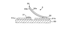
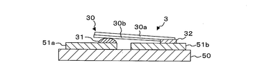
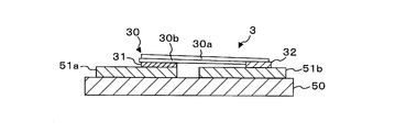
- FIGS. 2B and 2C are cross-sectional views illustrating a configuration example of the protection switch 3 according to the first embodiment.
- 2A shows the protection switch 3 in the off state (non-operation state)
- FIGS. 2B and 2C show the protection switch 3 in the on state (operation state).
- the protection switch 3 according to the first embodiment is provided between the bus bars 51a and 51b that are formed on the substrate 50 apart from each other.
- the bus bars 51a and 51b are made of a conductive material, and the electric wires 40 are connected to the bus bars 51a and 51b, respectively. For example, in the electric wire 40 shown in FIG.
- the electric wire 40 connected to the left side of the switch circuit 1 is connected to the bus bar 51a, and the electric wire 40 connected to the right side of the switch circuit 1 is connected to the bus bar 51b.
- the protection switch 3 turns on or off the connection between the bus bars 51a and 51b, the connection between the batteries 41 and 43 via the electric wire 40 is turned on or off.
- the semiconductor switch 2 is also provided to turn on or off the connection between the bus bars 51a and 51b.
- one end of the protection switch 3 is fixed (connected) to the first terminal 31 provided on the upper surface of the bus bar 51a, the second terminal 32 provided on the upper surface of the bus bar 51b, and the second terminal 32.
- a rectangular conductive plate 30 The first terminal 31 and the second terminal 32 (terminal pair) are made of a conductive material, and are connected to the electric wire 40 via bus bars 51a and 51b, respectively.
- the conductive plate 30 is formed of a bimetal formed by bonding two metal thin films (conductive members) 30a and 30b having different thermal expansion coefficients.
- the conductive plate 30 is attached to the substrate 50 (the bus bar 51b) with only one end connected to the second terminal 32. Normally, as shown in FIG. 2A, the other end of the conductive plate 30 is the first terminal. 31 is not connected. That is, in the normal state, the protection switch 3 is in an off state (non-operating state), and the first terminal 31 and the second terminal 32 are not electrically connected.
- the conductive plate 30 is configured to be deformed as the ambient temperature rises.
- the conductive plate 30 is deformed from a warped shape as shown in FIG. 2A to a linear shape as shown in FIGS. 2B and 2C. Is configured to do.
- the conductive plate 30 shown in FIGS. 2A to 2C is attached, for example, with the metal thin film 30a having a high coefficient of thermal expansion facing upward.
- the protection switch 3 is turned on (operating state) to turn on the connection between the batteries 41 and 43.
- the temperature at which the conductive plate 30 is deformed may be set so that the protection switch 3 operates before the semiconductor switch 2 is overheated according to the specifications of the semiconductor switch 2.
- the conductive plate 30 is composed of metal thin films 30a and 30b made by adding manganese, chromium, copper, etc. to an alloy of iron and nickel, for example, and the temperature at which the conductive plate 30 is deformed is a metal thin film. It can be arbitrarily set depending on the materials 30a and 30b and the content of each material.
- the temperature at which the other end of the conductive plate 30 is connected to the first terminal 31 can also be adjusted by adjusting the initial shape.
- the protective switch 3 is preferably arranged in the vicinity of the semiconductor switch 2 so that the ambient temperature of the protective switch 3 is close to the temperature of the semiconductor switch 2.
- the protection switch 3 having the above-described configuration, for example, when the semiconductor switch 2 (semiconductor element) abnormally generates heat due to a large current flowing through the semiconductor switch 2, the conductive plate 30 is deformed as the temperature of the semiconductor switch 2 rises. Then, as shown in FIG. 2B, when the other end of the conductive plate 30 comes into contact with the first terminal 31, the protection switch 3 is turned on (operated). When the protection switch 3 is activated, a large current flowing through the semiconductor switch 2 is shunted to the protection switch 3, so that the current flowing through the semiconductor switch 2 is reduced and the semiconductor element and surrounding components can be prevented from being overheated.
- the protective switch 3 in operation is deformed so that the conductive plate 30 returns to its original shape as the temperature of the semiconductor switch 2 decreases. That is, the conductive plate 30 having the shape shown in FIG. 2B is deformed into the shape shown in FIG. 2A. Then, as shown in FIG. 2A, when the other end of the conductive plate 30 is separated from the first terminal 31, the protection switch 3 is turned off to turn off the connection between the batteries 41 and 43, and returns to the normal state.
- the metal thin films 30a and 30b and the first terminal 31 and the second terminal 32 constituting the conductive plate 30 are made of a conductive material having a small electric resistance. Thereby, when the protection switch 3 operates, the current flowing through the semiconductor switch 2 can be further reduced. Further, one end of the conductive plate 30 and the second terminal 32 are fixed using solder, screws or the like. It is preferable that a member for fixing one end of the conductive plate 30 and the second terminal 32 is also made of a conductive material having a small electric resistance.
- the first terminal 31 may be composed of a melting member that melts at a predetermined temperature.
- the first terminal 31 can be composed of a melting member that melts at a temperature higher than the temperature at which the protection switch 3 operates (the temperature at which the conductive plate 30 is deformed). In this case, when the temperature of the semiconductor switch 2 (semiconductor element) further rises and reaches the melting temperature of the first terminal 31 after the protection switch 3 is turned on as shown in FIG. As shown, the first terminal 31 melts.
- solder can be used as the melting member. When solder is used, the electrical resistance of the first terminal 31 after melting is reduced.
- the semiconductor switch 2 When the semiconductor switch 2 is overheated to the extent that the melting member (the first terminal 31) is melted, the possibility that the semiconductor switch 2 is restored is low. Therefore, when the situation where the first terminal 31 melts occurs, the electric resistance flowing through the semiconductor switch 2 can be further reduced by further reducing the electrical resistance of the first terminal 31.
- the protection switch 3 When the temperature of the semiconductor switch 2 is lowered after the first terminal 31 is melted and the first terminal 31 is solidified, the other end of the conductive plate 30 and the first terminal 31 are solidified. 1 terminal 31), the protection switch 3 is kept on. Therefore, in this case, since the connection between the batteries 41 and 43 via the protection switch 3 as well as the semiconductor switch 2 having a low possibility of recovery can be maintained, the normal operation of the power supply device can be performed. In addition, since solder becomes low resistance when solidified after being melted, it is preferably used as a melting member.
- the protection switch 3 is composed of a conductive plate 30 using bimetal. Since the bimetal can be adjusted to be deformed at an arbitrary temperature, the protection switch 3 that operates at an arbitrary temperature can be easily realized. Therefore, the protection switch 3 suitable for the environment in which it is arranged can be configured, and the switch circuit 1 provided with the appropriate protection switch 3 and the power supply device can be installed.
- the conductive plate 30 is not limited to a configuration using a bimetal obtained by bonding two types of metal thin films 30a and 30b. As long as it can be deformed at an arbitrary temperature, the conductive plate 30 may be configured by laminating three or more types of metal thin films, or the conductive plate 30 may be configured with one type of metal thin film like a shape memory alloy. Also good.
- Embodiment 2 Since the power supply device of Embodiment 2 has the same configuration as that of the power supply device of Embodiment 1 except for the configuration of the protection switch 3, the same components are denoted by the same reference numerals and description thereof is omitted.
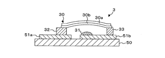
- 3A to 3C are cross-sectional views illustrating a configuration example of the protection switch 3 according to the second embodiment.
- 3A shows the protection switch 3 in the off state (non-operation state)
- FIGS. 3B and 3C show the protection switch 3 in the on state (operation state).
- symbol and a name are attached
- the protection switch 3 of the second embodiment is also provided between the bus bars 51a and 51b formed on the substrate 50.
- the protection switch 3 according to the second embodiment includes a first terminal 31 provided on the upper surface of the bus bar 51b, a second terminal 32 provided on the upper surface of the bus bar 51a, and a conductive plate 30. Further, the protection switch 3 according to the second embodiment includes an insulating support 33 made of an insulating material at a position facing the second terminal 32 with the first terminal 31 interposed therebetween on the upper surface of the bus bar 51b. As shown in FIG.
- the conductive plate 30 of Embodiment 2 is formed in a curved rectangular plate shape, one end is fixed to the second terminal 32, the other end is fixed to the insulating support 33, and the upper side is It is attached to the board
- the conductive plate 30, the first terminal 31, and the second terminal 32 have the same configuration as the conductive plate 30, the first terminal 31, and the second terminal 32 of the first embodiment, respectively.
- one end of the conductive plate 30 and the second terminal 32 are fixed using solder or screws, and the member to be fixed is preferably made of a conductive material having a low electrical resistance.
- both ends of the conductive plate 30 of the second embodiment are fixed to the second terminal 32 and the insulating support 33, when the ambient temperature rises, the shape of the conductive plate 30 curved upward as shown in FIG. As shown in FIG. 3C, it is configured to be deformed into a downward curved shape. Note that the conductive plate 30 can be deformed in this manner by attaching the conductive plate 30 with the metal thin film 30a having a large coefficient of thermal expansion facing upward.
- the protection switch 3 having the above-described configuration, when the semiconductor switch 2 (semiconductor element) abnormally generates heat, the conductive plate 30 is deformed as the temperature of the semiconductor switch 2 rises, and as shown in FIG. When the lower surface of 30b comes into contact with the first terminal 31, it is turned on (operated). As a result, the first terminal 31 and the second terminal 32 are connected, and the connection between the batteries 41 and 43 is turned on. Also in the second embodiment, when the protection switch 3 is activated, a large current flowing through the semiconductor switch 2 is shunted to the protection switch 3, so that the current flowing through the semiconductor switch 2 is reduced and the semiconductor element is prevented from being overheated. it can.
- the protection switch 3 in operation, when the temperature of the semiconductor switch 2 is lowered, the conductive plate 30 is deformed so as to return to the original shape, and the lower surface of the conductive plate 30 is the first terminal 31 as shown in FIG. 3A. At the time of leaving, the protection switch 3 is turned off and returns to the normal state.
- the energy required for deformation differs between when the shape shown in FIG. 3A is changed to the shape shown in FIG. 3B and when the shape shown in FIG. 3B returns to the shape shown in FIG. 3A.
- the protection switch 3 can be configured to switch from the on state to the off state at a temperature lower than the temperature at the time of switching from the off state to the on state. . Thereby, it is possible to prevent the protection switch 3 from being frequently turned on / off. Further, in the protection switch 3 of the second embodiment, as shown in FIG. 3A, both ends of the conductive plate 30 are fixed to the second terminal 32 and the insulating support 33 in a curved state.
- the metal thin film 30a having a large coefficient of thermal expansion pushes the metal thin film 30b downward, and the pressing force by the metal thin film 30a becomes a predetermined value or more, the state shown in FIG. 3B Transforms into That is, hysteresis can be created in the protective switch 3, and this deformation utilizes a phenomenon called buckling.
- the first terminal 31 can be configured by a melting member that melts at a predetermined temperature (a temperature higher than the temperature at which the protection switch 3 operates).
- a predetermined temperature a temperature higher than the temperature at which the protection switch 3 operates.
- the temperature of the semiconductor switch 2 is lowered after the first terminal 31 is melted and the first terminal 31 is solidified, the lower surface of the conductive plate 30 and the first terminal 31 are solidified by the molten member (first Since the connection is made at the terminal 31), the ON state of the protection switch 3 can be maintained.
- the conductive plate 30 is not limited to a configuration using a bimetal, and may be configured by bonding three or more types of metal thin films, or one type of metal thin film such as a shape memory alloy. You may comprise.
Landscapes
- Engineering & Computer Science (AREA)
- Power Engineering (AREA)
- Physics & Mathematics (AREA)
- Thermal Sciences (AREA)
- Fuses (AREA)
- Thermally Actuated Switches (AREA)
- Direct Current Feeding And Distribution (AREA)
- Charge And Discharge Circuits For Batteries Or The Like (AREA)
- Electronic Switches (AREA)
- Connection Of Batteries Or Terminals (AREA)
Abstract
複数のバッテリを接続する電線に介装されるスイッチ回路は、バッテリ間の接続をオン又はオフする半導体スイッチと、半導体スイッチに並列に接続される保護スイッチとを含む。保護スイッチは、電線にそれぞれ接続された端子対と、熱膨張率が異なる複数の導電部材を貼り合わせた導電板とを有する。導電板は、半導体スイッチの温度上昇に伴って端子間を接続するように変形し、電源間の接続をオンする。
Description
本発明は、スイッチ回路及び電源装置に関する。
本出願は、2016年11月15日出願の日本特許出願第2016-222506号に基づく優先権を主張し、前記日本特許出願に記載された全ての記載内容を援用するものである。
本出願は、2016年11月15日出願の日本特許出願第2016-222506号に基づく優先権を主張し、前記日本特許出願に記載された全ての記載内容を援用するものである。
特許文献1には、基板上に溶融部材を介して導通部材が設けてあり、半導体スイッチの異常発熱時に溶融部材が溶融することで導通部材が基板上まで変位し、基板上に設けられた2つの端子に接触することによって、端子間を電気的に接続する保護回路が開示されている。
本開示のスイッチ回路は、複数の電源を接続する電線に介装されるスイッチ回路において、前記電線に介装され、前記複数の電源間の接続をオン又はオフする半導体スイッチと、前記半導体スイッチに並列に接続され、前記半導体スイッチの温度上昇に伴って変形することにより前記電源間の接続をオンする保護スイッチとを備える。
本開示の電源装置は、複数の電源と、上述のスイッチ回路とを備える。
[本開示が解決しようとする課題]
特許文献1に開示された保護回路では、溶融部材が溶融することで端子間が電気的に接続されるので、端子間が接続される温度(保護回路が作動する温度)は溶融部材の融点により決まる。しかしながら、所望の融点を実現できる素材を都合よく選定できるとは限らない。例えば、溶融部材に鉛フリーはんだを用いる必要がある場合、融点の調整が難しく、所望の融点の溶融部材を実現することは困難である。従って、保護回路が作動する温度を任意に設定することは容易ではない。
特許文献1に開示された保護回路では、溶融部材が溶融することで端子間が電気的に接続されるので、端子間が接続される温度(保護回路が作動する温度)は溶融部材の融点により決まる。しかしながら、所望の融点を実現できる素材を都合よく選定できるとは限らない。例えば、溶融部材に鉛フリーはんだを用いる必要がある場合、融点の調整が難しく、所望の融点の溶融部材を実現することは困難である。従って、保護回路が作動する温度を任意に設定することは容易ではない。
本発明は、斯かる事情に鑑みてなされたものであり、その目的とするところは、任意の温度で作動する保護回路を備えたスイッチ回路及び電源装置を提供する。
[本開示の効果]
本開示によれば、任意の温度で作動する保護スイッチを備えたスイッチ回路及び電源装置を提供することが可能となる。
本開示によれば、任意の温度で作動する保護スイッチを備えたスイッチ回路及び電源装置を提供することが可能となる。
[本発明の実施形態の説明]
最初に本発明の実施態様を列記して説明する。また、以下に記載する実施形態の少なくとも一部を任意に組み合わせてもよい。
最初に本発明の実施態様を列記して説明する。また、以下に記載する実施形態の少なくとも一部を任意に組み合わせてもよい。
(1)本発明の一態様に係るスイッチ回路は、複数の電源を接続する電線に介装されるスイッチ回路において、前記電線に介装され、前記複数の電源間の接続をオン又はオフする半導体スイッチと、前記半導体スイッチに並列に接続され、前記半導体スイッチの温度上昇に伴って変形することにより前記電源間の接続をオンする保護スイッチとを備える。
本態様にあっては、半導体スイッチに並列に設けられる保護スイッチが、半導体スイッチの温度上昇に伴って変形することによって電源間の接続をオンする。温度上昇に伴う変形によって電源間の接続をオンする保護スイッチは、溶融部材の溶融によって端子間が接続される構成よりも、作動する温度の設定が容易である。よって、任意の温度で作動する保護スイッチを備えたスイッチ回路の実現が可能である。
(2)前記保護スイッチは、前記電線にそれぞれ接続された端子対と、熱膨張率が異なる複数の導電部材を貼り合わせた導電板とを有し、前記導電板は、前記端子対の一方の端子に接続されており、前記半導体スイッチの温度上昇に伴って前記端子対の前記一方の端子及び他方の端子間を接続するように変形する構成が好ましい。
本態様にあっては、保護スイッチは、熱膨張率が異なる複数の導電部材を貼り合わせた導電板で構成してある。導電板は、半導体スイッチの温度上昇に伴って変形し、変形した導電板が端子間を接続する。例えば2種類の金属薄膜を貼り合わせたバイメタルは、変形する際の温度を容易に設定できるので、任意の温度で作動する保護スイッチの実現が可能である。
(3)前記端子対の少なくとも前記他方の端子は、導電性を有し所定の温度で溶融する溶融部材で構成されていることが好ましい。
本態様にあっては、作動(変形)した保護スイッチが接続する端子が、所定の温度で溶融する溶融部材で構成されている。よって、所定の温度以上になった場合に溶融部材の端子が溶融することにより、端子の電気抵抗の低減が可能である。
(4)前記保護スイッチは、前記電源間の接続をオンしている場合、前記半導体スイッチの温度低下に伴って元の形状に戻るように変形することにより前記電源間の接続をオフする構成が好ましい。
本態様にあっては、作動した保護スイッチは、半導体スイッチの温度低下に伴って元の形状に変形することによって電源間の接続をオフする。よって、保護スイッチが作動することによって半導体スイッチの温度が低下した場合には、保護スイッチによる電源間の接続がオフされ、半導体スイッチによる電源間の接続のみが行われる。
(5)前記保護スイッチは、前記電源間の接続をオンする際の温度よりも低い温度で前記電源間の接続をオフする構成が好ましい。
本態様にあっては、保護スイッチは、電源間の接続をオンする際の温度よりも低い温度で電源間の接続をオフする。よって、保護スイッチにて電源間が一旦接続された場合、電源間の接続がオフされる温度に下がるまで、電源間の接続が維持されるので、電源間の接続が頻繁にオン/オフされることを防止できる。
(6)本発明の一態様に係る電源装置は、複数の電源と、上述のいずれかのスイッチ回路とを備える。
本態様にあっては、任意の温度で作動する保護スイッチを備えたスイッチ回路を介して、複数の電源が接続される。
[本発明の実施形態の詳細]
近年、複数のバッテリを備えた電源システムが車両に搭載されるようになった。このような電源システムでは、バッテリ間の電気的接続をオン/オフするためのスイッチが設けられている。バッテリ間に設けられるスイッチは、頻繁にオン/オフされるため、メカニカルリレーよりも開閉寿命が長い半導体リレー(半導体スイッチ)が用いられることがある。一方で、半導体スイッチを用いた場合、短絡等によってスイッチに過大な電流が流れたときに、半導体素子が発熱し、この発熱によって半導体素子自体や周辺の部品が破損する虞がある。そのため、半導体スイッチを用いる場合、スイッチを構成する部品が耐熱温度まで上昇する前にスイッチをオフする構成が設けられている。また、不測の事態が発生してスイッチをオフできなくなった場合にスイッチを保護する保護回路も設けられている。例えば、保護回路は、半導体スイッチに並列に接続され、半導体スイッチに流れる電流を保護回路に分流することによって半導体スイッチに流れる電流を減らすように構成されている。
近年、複数のバッテリを備えた電源システムが車両に搭載されるようになった。このような電源システムでは、バッテリ間の電気的接続をオン/オフするためのスイッチが設けられている。バッテリ間に設けられるスイッチは、頻繁にオン/オフされるため、メカニカルリレーよりも開閉寿命が長い半導体リレー(半導体スイッチ)が用いられることがある。一方で、半導体スイッチを用いた場合、短絡等によってスイッチに過大な電流が流れたときに、半導体素子が発熱し、この発熱によって半導体素子自体や周辺の部品が破損する虞がある。そのため、半導体スイッチを用いる場合、スイッチを構成する部品が耐熱温度まで上昇する前にスイッチをオフする構成が設けられている。また、不測の事態が発生してスイッチをオフできなくなった場合にスイッチを保護する保護回路も設けられている。例えば、保護回路は、半導体スイッチに並列に接続され、半導体スイッチに流れる電流を保護回路に分流することによって半導体スイッチに流れる電流を減らすように構成されている。
以下に、本発明の一態様に係るスイッチ回路及び電源装置について、実施形態を示す図面を参照しつつ説明する。なお、本発明はこれらの例示に限定されるものではなく、請求の範囲によって示され、請求の範囲と均等の意味および範囲内でのすべての変更が含まれることが意図される。
(実施形態1)
図1は、実施形態1に係る電源装置の構成例を示すブロック図である。実施形態1の電源装置は車両に搭載されている。また、実施形態1の電源装置は、2つの第1バッテリ41及び第2バッテリ43(電源)を備えており、バッテリ41,43を接続する電線40に介装されたスイッチ回路1を有する。なお、バッテリ41,43はスイッチ回路1を介して並列に接続される。車両に搭載される電源装置は、3つ以上のバッテリを備える構成でもよく、この場合、それぞれのバッテリ間を接続する電線にスイッチ回路が介装される。
図1は、実施形態1に係る電源装置の構成例を示すブロック図である。実施形態1の電源装置は車両に搭載されている。また、実施形態1の電源装置は、2つの第1バッテリ41及び第2バッテリ43(電源)を備えており、バッテリ41,43を接続する電線40に介装されたスイッチ回路1を有する。なお、バッテリ41,43はスイッチ回路1を介して並列に接続される。車両に搭載される電源装置は、3つ以上のバッテリを備える構成でもよく、この場合、それぞれのバッテリ間を接続する電線にスイッチ回路が介装される。
実施形態1の電源装置において、第1バッテリ41にはカーナビゲーションシステム等の車載機器である負荷42が並列に接続されている。また、第2バッテリ43には、車両のエンジンを始動させるためのスタータ44が並列に接続されている。第1バッテリ41及び第2バッテリ43には、負荷42及びスタータ44以外の負荷が更に並列に接続されていてもよい。
スイッチ回路1は、電線40に介装され、バッテリ41,43間の接続をオン又はオフする半導体スイッチ2と、半導体スイッチ2のオン又はオフを制御するスイッチ制御部20と、半導体スイッチ2に並列に接続された保護スイッチ3とを含む。図1は、半導体スイッチ2がNチャネル型FET(Field Effect Transistor)で構成されている例を示しているが、半導体スイッチ2はPチャネル型FETで構成することもできる。
スイッチ制御部20は、第1バッテリ41と第2バッテリ43との接続を遮断すべきときに半導体スイッチ2をオフする。例えば、スイッチ制御部20には、スタータ44がエンジンを始動させる際に事前に通知信号が入力される。通知信号が入力された場合、スイッチ制御部20は、半導体スイッチ2をオフし、第1バッテリ41と第2バッテリ43との接続を遮断する。
スタータ44はエンジンを始動させる際に大量の電流を必要とするので、エンジン始動時に大きな電圧変動が生じる。よって、スタータ44(第2バッテリ43)側で生じる電圧変動による影響が第1バッテリ41及び負荷42に及ばないように、上述のようにスタータ44によるエンジン始動の直前に第1バッテリ41と第2バッテリ43との接続を遮断しておく。
スタータ44はエンジンを始動させる際に大量の電流を必要とするので、エンジン始動時に大きな電圧変動が生じる。よって、スタータ44(第2バッテリ43)側で生じる電圧変動による影響が第1バッテリ41及び負荷42に及ばないように、上述のようにスタータ44によるエンジン始動の直前に第1バッテリ41と第2バッテリ43との接続を遮断しておく。
スイッチ制御部20は、第2バッテリ43の電圧が回復した後、半導体スイッチ2をオンし、第1バッテリ41と第2バッテリ43との接続を再開する。なお、スイッチ制御部20は、通常時では、半導体スイッチ2をオンしており、これにより、通常時は2つのバッテリ41,43からの電力が負荷42等に供給される。
実施形態1の電源装置において、例えば第2バッテリ43側で短絡が生じた場合、第1バッテリ41から半導体スイッチ2及び短絡経路を大電流が流れる状況が発生する。半導体スイッチ2に大電流が流れた場合、半導体スイッチ2を構成する半導体素子が発熱し、半導体素子自体や周辺の部品が過熱状態となり、各部品が破損する虞がある。
そこで、実施形態1の電源装置では、各部品が過熱状態となる前に保護スイッチ3が作動し、保護スイッチ3を介したバッテリ41,43間の接続がオンされるように構成してある。保護スイッチ3が作動した場合、半導体スイッチ2に流れる大電流が保護スイッチ3に分流されるので、半導体スイッチ2に流れる電流を減らすことができる。その結果、半導体素子の発熱が抑えられ、各部品の破損を防止できる。
そこで、実施形態1の電源装置では、各部品が過熱状態となる前に保護スイッチ3が作動し、保護スイッチ3を介したバッテリ41,43間の接続がオンされるように構成してある。保護スイッチ3が作動した場合、半導体スイッチ2に流れる大電流が保護スイッチ3に分流されるので、半導体スイッチ2に流れる電流を減らすことができる。その結果、半導体素子の発熱が抑えられ、各部品の破損を防止できる。
図2A乃至図2Cは、実施形態1の保護スイッチ3の構成例を示す断面図である。図2Aはオフ状態(非作動状態)の保護スイッチ3を示し、図2B,図2Cはオン状態(作動状態)の保護スイッチ3を示す。
実施形態1の保護スイッチ3は、基板50上に離れて形成されたバスバー51a,51b間に設けられている。バスバー51a,51bは導電性材料で構成されており、バスバー51a,51bのそれぞれには電線40が接続されている。例えば、図1に示す電線40において、スイッチ回路1の左側に接続されている電線40は、バスバー51aに接続されており、スイッチ回路1の右側に接続されている電線40は、バスバー51bに接続されている。このような構成において、保護スイッチ3がバスバー51a,51b間の接続をオン又はオフすることにより、電線40を介したバッテリ41,43間の接続がオン又はオフされる。なお、半導体スイッチ2も、バスバー51a,51b間の接続をオン又はオフするように設けられている。
実施形態1の保護スイッチ3は、基板50上に離れて形成されたバスバー51a,51b間に設けられている。バスバー51a,51bは導電性材料で構成されており、バスバー51a,51bのそれぞれには電線40が接続されている。例えば、図1に示す電線40において、スイッチ回路1の左側に接続されている電線40は、バスバー51aに接続されており、スイッチ回路1の右側に接続されている電線40は、バスバー51bに接続されている。このような構成において、保護スイッチ3がバスバー51a,51b間の接続をオン又はオフすることにより、電線40を介したバッテリ41,43間の接続がオン又はオフされる。なお、半導体スイッチ2も、バスバー51a,51b間の接続をオン又はオフするように設けられている。
具体的には、保護スイッチ3は、バスバー51aの上面に設けられた第1端子31と、バスバー51bの上面に設けられた第2端子32と、第2端子32に一端が固定(接続)された矩形の導電板30とを含む。第1端子31及び第2端子32(端子対)は、導電性材料で形成されており、それぞれバスバー51a,51bを介して電線40に接続される。
導電板30は、熱膨張率が異なる2つの金属薄膜(導電部材)30a,30bを貼り合わせて構成されたバイメタルで形成されている。導電板30は、一端のみが第2端子32に接続された状態で基板50(バスバー51b)に取り付けられており、通常時では図2Aに示すように、導電板30の他端は第1端子31に接続されていない。即ち、通常時では、保護スイッチ3はオフ状態(非作動状態)であり、第1端子31及び第2端子32は電気的に接続されない。
導電板30は、熱膨張率が異なる2つの金属薄膜(導電部材)30a,30bを貼り合わせて構成されたバイメタルで形成されている。導電板30は、一端のみが第2端子32に接続された状態で基板50(バスバー51b)に取り付けられており、通常時では図2Aに示すように、導電板30の他端は第1端子31に接続されていない。即ち、通常時では、保護スイッチ3はオフ状態(非作動状態)であり、第1端子31及び第2端子32は電気的に接続されない。
導電板30は、周辺温度の上昇に伴って変形するように構成されており、実施形態1では、図2Aに示すように反った形状から、図2B,図2Cに示すように直線形状に変形するように構成されている。図2A乃至図2Cに示す導電板30は、例えば熱膨張率が大きい金属薄膜30aを上側にして取り付けられている。
保護スイッチ3は、導電板30が変形して導電板30の他端が第1端子31に接続することによってバッテリ41,43間の接続をオンするオン状態(作動状態)となる。従って、半導体スイッチ2の仕様に応じて半導体スイッチ2が過熱状態となる前に保護スイッチ3が作動するように、導電板30が変形する温度を設定すればよい。なお、導電板30は、例えば鉄及びニッケルの合金に、マンガン、クロム、銅等を添加して作られた金属薄膜30a,30bで構成されており、導電板30が変形する温度は、金属薄膜30a,30bの材料及び各材料の含有量によって任意に設定できる。また、初期形状の調整によっても、導電板30の他端が第1端子31に接続する温度を調整できる。なお、保護スイッチ3の周辺温度が半導体スイッチ2の温度と近い温度となるように、保護スイッチ3は半導体スイッチ2の近傍に配置することが好ましい。
保護スイッチ3は、導電板30が変形して導電板30の他端が第1端子31に接続することによってバッテリ41,43間の接続をオンするオン状態(作動状態)となる。従って、半導体スイッチ2の仕様に応じて半導体スイッチ2が過熱状態となる前に保護スイッチ3が作動するように、導電板30が変形する温度を設定すればよい。なお、導電板30は、例えば鉄及びニッケルの合金に、マンガン、クロム、銅等を添加して作られた金属薄膜30a,30bで構成されており、導電板30が変形する温度は、金属薄膜30a,30bの材料及び各材料の含有量によって任意に設定できる。また、初期形状の調整によっても、導電板30の他端が第1端子31に接続する温度を調整できる。なお、保護スイッチ3の周辺温度が半導体スイッチ2の温度と近い温度となるように、保護スイッチ3は半導体スイッチ2の近傍に配置することが好ましい。
上述した構成の保護スイッチ3は、例えば半導体スイッチ2に大電流が流れることによって半導体スイッチ2(半導体素子)が異常発熱した場合、半導体スイッチ2の温度上昇に伴って導電板30が変形する。そして、図2Bに示すように導電板30の他端が第1端子31に接触した時点で、保護スイッチ3がオン状態となる(作動する)。保護スイッチ3が作動した場合、半導体スイッチ2に流れる大電流が保護スイッチ3に分流されるので、半導体スイッチ2に流れる電流が減り、半導体素子及び周囲の部品が過熱状態となることを回避できる。
半導体スイッチ2に流れる電流が減少した場合、半導体スイッチ2(半導体素子)の温度が低下してくる。よって、作動中の保護スイッチ3において、半導体スイッチ2の温度低下に伴って導電板30が元の形状に戻るように変形する。即ち、図2Bに示す形状の導電板30が、図2Aに示す形状に変形する。そして、図2Aに示すように導電板30の他端が第1端子31から離れた時点で、保護スイッチ3は、バッテリ41,43間の接続をオフするオフ状態となり、通常状態に戻る。
導電板30を構成する金属薄膜30a,30b、並びに、第1端子31及び第2端子32は、電気抵抗が小さい導電性材料で構成されることが好ましい。これにより、保護スイッチ3が作動した場合に、半導体スイッチ2に流れる電流をより減らすことができる。また、導電板30の一端と第2端子32とは、はんだ又はビス等を用いて固定されている。導電板30の一端と第2端子32とを固定する部材も電気抵抗が小さい導電性材料で構成されていることが好ましい。
第1端子31は、所定の温度で溶融する溶融部材で構成してもよい。例えば、保護スイッチ3が作動する温度(導電板30が変形する温度)よりも高い温度で溶融する溶融部材で第1端子31を構成することができる。この場合、図2Bに示すように保護スイッチ3がオン状態となってから、更に半導体スイッチ2(半導体素子)の温度が上昇して第1端子31の溶融温度に到達した場合に、図2Cに示すように第1端子31が溶融する。溶融部材としては例えばはんだを用いることができ、はんだを用いた場合、第1端子31の溶融後の電気抵抗が低減する。溶融部材(第1端子31)が溶融する程に半導体スイッチ2が過熱状態となった場合、半導体スイッチ2が復旧する可能性は低い。よって、第1端子31が溶融する状況が生じた場合には、第1端子31の電気抵抗をより低減させることにより、半導体スイッチ2に流れる電流の更なる低減を図ることができる。なお、第1端子31が溶融した後に半導体スイッチ2の温度が低下して第1端子31が固化した場合には、導電板30の他端と第1端子31とが、固化した溶融部材(第1端子31)で接続されるので、保護スイッチ3のオン状態が維持される。よって、この場合、復旧する可能性が低い半導体スイッチ2だけでなく保護スイッチ3を介したバッテリ41、43間の接続が維持できるので、電源装置の通常動作が可能となる。なお、はんだは溶融した後に固化した場合、低抵抗となるので、溶融部材として用いることが好ましい。
実施形態1では、保護スイッチ3が、バイメタルを用いた導電板30で構成されている。バイメタルは、任意の温度で変形するように調整できるので、任意の温度で作動する保護スイッチ3を容易に実現できる。よって、配置される環境に適切な保護スイッチ3を構成でき、適切な保護スイッチ3が設けられたスイッチ回路1及び電源装置の設置が可能となる。
なお、導電板30は、2種類の金属薄膜30a,30bを貼り合わせたバイメタルを用いる構成に限らない。任意の温度で変形するものであれば、3種類以上の金属薄膜を貼り合わせて導電板30を構成してもよく、形状記憶合金のように1種類の金属薄膜で導電板30を構成してもよい。
なお、導電板30は、2種類の金属薄膜30a,30bを貼り合わせたバイメタルを用いる構成に限らない。任意の温度で変形するものであれば、3種類以上の金属薄膜を貼り合わせて導電板30を構成してもよく、形状記憶合金のように1種類の金属薄膜で導電板30を構成してもよい。
(実施形態2)
実施形態2の電源装置は、保護スイッチ3の構成以外は実施形態1の電源装置と同様の構成を有するので、同様の構成については同一の符号を付して説明を省略する。
図3A乃至図3Cは、実施形態2の保護スイッチ3の構成例を示す断面図である。図3Aはオフ状態(非作動状態)の保護スイッチ3を示し、図3B,図3Cはオン状態(作動状態)の保護スイッチ3を示す。なお、保護スイッチ3においても、実施形態1と同様の構成については同一の符号及び名称を付す。
実施形態2の電源装置は、保護スイッチ3の構成以外は実施形態1の電源装置と同様の構成を有するので、同様の構成については同一の符号を付して説明を省略する。
図3A乃至図3Cは、実施形態2の保護スイッチ3の構成例を示す断面図である。図3Aはオフ状態(非作動状態)の保護スイッチ3を示し、図3B,図3Cはオン状態(作動状態)の保護スイッチ3を示す。なお、保護スイッチ3においても、実施形態1と同様の構成については同一の符号及び名称を付す。
実施形態2の保護スイッチ3も、基板50上に形成されたバスバー51a,51b間に設けられている。実施形態2の保護スイッチ3は、バスバー51bの上面に設けられた第1端子31と、バスバー51aの上面に設けられた第2端子32と、導電板30とを含む。また実施形態2の保護スイッチ3は、バスバー51bの上面において、第1端子31を挟んで第2端子32に対向する位置に、絶縁性材料で構成された絶縁支持体33を有する。実施形態2の導電板30は、図3Aに示すように、湾曲した矩形板状に形成してあり、一端が第2端子32に固定され、他端が絶縁支持体33に固定され、上側に湾曲した状態で基板50(バスバー51a,51b)に取り付けられている。よって、導電板30の一端は第2端子32及びバスバー51aを介して電線40に電気的に接続されているが、他端は第1端子31及びバスバー51b(電線40)に電気的に接続されていない。即ち、通常時では、保護スイッチ3はオフ状態(非作動状態)であり、第1端子31及び第2端子32は電気的に接続されていない。
導電板30、第1端子31及び第2端子32はそれぞれ、実施形態1の導電板30、第1端子31及び第2端子32と同様の構成を有する。また、導電板30の一端と第2端子32とは、はんだ又はビス等を用いて固定されており、固定する部材は電気抵抗が小さい導電性材料で構成されていることが好ましい。
実施形態2の導電板30は、両端が第2端子32及び絶縁支持体33に固定されているので、周辺温度が上昇した場合、図3Aに示すように上側に湾曲した形状から、図3B,図3Cに示すように下側に湾曲した形状に変形するように構成されている。なお、熱膨張率が大きい金属薄膜30aを上側にして導電板30を取り付けることにより、導電板30はこのような変形を行うことができる。
上述した構成の保護スイッチ3は、半導体スイッチ2(半導体素子)が異常発熱した場合、半導体スイッチ2の温度上昇に伴って導電板30が変形し、図3Bに示すように導電板30(金属薄膜30b)の下面が第1端子31に接触した時点でオン状態となる(作動する)。これにより、第1端子31と第2端子32との間が接続され、バッテリ41,43間の接続がオンされる。実施形態2においても、保護スイッチ3が作動した場合、半導体スイッチ2に流れる大電流が保護スイッチ3に分流されるので、半導体スイッチ2に流れる電流が減り、半導体素子が過熱状態となることを回避できる。
また、作動中の保護スイッチ3において、半導体スイッチ2の温度が低下した場合、導電板30が元の形状に戻るように変形し、図3Aに示すように導電板30の下面が第1端子31から離れた時点で、保護スイッチ3がオフ状態となり、通常状態に戻る。
実施形態2の保護スイッチ3では、図3Aに示す形状から図3Bに示す形状に変形する場合と、図3Bに示す形状から図3Aに示す形状に戻る場合とでは、変形に要するエネルギーが異なる。よって、金属薄膜30a,30bの熱膨張率を適切に設定することにより、保護スイッチ3を、オフ状態からオン状態に切り替わる際の温度よりも低い温度でオン状態からオフ状態に切り替わるように構成できる。これにより、保護スイッチ3が頻繁にオン/オフされることを防止できる。
また、実施形態2の保護スイッチ3では、図3Aに示すように導電板30は湾曲した状態で両端が第2端子32及び絶縁支持体33に固定されている。よって、半導体スイッチ2が異常発熱した場合に、熱膨張率が大きい金属薄膜30aが金属薄膜30bを下向きに押し、金属薄膜30aによる押圧力が所定値以上となった場合に、図3Bに示す状態に変形する。即ち、保護スイッチ3にヒステリシスを作ることができ、この変形は座屈と呼ばれる現象を利用している。
実施形態2の保護スイッチ3では、図3Aに示す形状から図3Bに示す形状に変形する場合と、図3Bに示す形状から図3Aに示す形状に戻る場合とでは、変形に要するエネルギーが異なる。よって、金属薄膜30a,30bの熱膨張率を適切に設定することにより、保護スイッチ3を、オフ状態からオン状態に切り替わる際の温度よりも低い温度でオン状態からオフ状態に切り替わるように構成できる。これにより、保護スイッチ3が頻繁にオン/オフされることを防止できる。
また、実施形態2の保護スイッチ3では、図3Aに示すように導電板30は湾曲した状態で両端が第2端子32及び絶縁支持体33に固定されている。よって、半導体スイッチ2が異常発熱した場合に、熱膨張率が大きい金属薄膜30aが金属薄膜30bを下向きに押し、金属薄膜30aによる押圧力が所定値以上となった場合に、図3Bに示す状態に変形する。即ち、保護スイッチ3にヒステリシスを作ることができ、この変形は座屈と呼ばれる現象を利用している。
実施形態2においても、第1端子31は、所定の温度(保護スイッチ3が作動する温度よりも高い温度)で溶融する溶融部材で構成することができる。この場合、図3Bに示すように保護スイッチ3がオン状態となってから、更に半導体スイッチ2(半導体素子)の温度が上昇して第1端子31の溶融温度に到達した場合に、図3Cに示すように第1端子31が溶融する。溶融部材としてはんだを用いた場合、半導体スイッチ2が復旧する可能性が低いときに、第1端子31(溶融部材)を溶融させることにより、第1端子31の電気抵抗をより低減させることができる。
また、第1端子31が溶融した後に半導体スイッチ2の温度が低下して第1端子31が固化した場合には、導電板30の下面と第1端子31とが、固化した溶融部材(第1端子31)で接続されるので、保護スイッチ3のオン状態を維持することができる。
また、第1端子31が溶融した後に半導体スイッチ2の温度が低下して第1端子31が固化した場合には、導電板30の下面と第1端子31とが、固化した溶融部材(第1端子31)で接続されるので、保護スイッチ3のオン状態を維持することができる。
実施形態2のスイッチ回路1においても、実施形態1のスイッチ回路1と同様の効果が得られる。また、実施形態2においても、導電板30は、バイメタルを用いる構成に限らず、3種類以上の金属薄膜を貼り合わせて構成してもよく、また、形状記憶合金のように1種類の金属薄膜で構成してもよい。
今回開示された実施形態はすべての点で例示であって、制限的なものではないと考えられるべきである。本発明の範囲は、上記した意味ではなく、請求の範囲によって示され、請求の範囲と均等の意味及び範囲内でのすべての変更が含まれることが意図される。
1 スイッチ回路
2 半導体スイッチ
3 保護スイッチ
30導電板
31 第1端子
32 第2端子
33 絶縁支持体
40 電線
41 第1バッテリ
43 第2バッテリ
30a,30b 金属薄膜
2 半導体スイッチ
3 保護スイッチ
30導電板
31 第1端子
32 第2端子
33 絶縁支持体
40 電線
41 第1バッテリ
43 第2バッテリ
30a,30b 金属薄膜
Claims (6)
- 複数の電源を接続する電線に介装されるスイッチ回路において、
前記電線に介装され、前記複数の電源間の接続をオン又はオフする半導体スイッチと、
前記半導体スイッチに並列に接続され、前記半導体スイッチの温度上昇に伴って変形することにより前記電源間の接続をオンする保護スイッチと
を備えるスイッチ回路。 - 前記保護スイッチは、
前記電線にそれぞれ接続された端子対と、
熱膨張率が異なる複数の導電部材を貼り合わせた導電板と
を有し、
前記導電板は、前記端子対の一方の端子に接続されており、前記半導体スイッチの温度上昇に伴って前記端子対の前記一方の端子及び他方の端子間を接続するように変形する
請求項1に記載のスイッチ回路。 - 前記端子対の少なくとも前記他方の端子は、導電性を有し所定の温度で溶融する溶融部材で構成されている請求項2に記載のスイッチ回路。
- 前記保護スイッチは、前記電源間の接続をオンしている場合、前記半導体スイッチの温度低下に伴って元の形状に戻るように変形することにより前記電源間の接続をオフする
請求項1から3までのいずれかひとつに記載のスイッチ回路。 - 前記保護スイッチは、前記電源間の接続をオンする際の温度よりも低い温度で前記電源間の接続をオフする
請求項4に記載のスイッチ回路。 - 複数の電源と、
請求項1から5までのいずれかひとつに記載のスイッチ回路と
を備える電源装置。
Priority Applications (2)
| Application Number | Priority Date | Filing Date | Title |
|---|---|---|---|
| CN201780067697.6A CN109923748B (zh) | 2016-11-15 | 2017-10-30 | 开关电路及电源装置 |
| US16/348,324 US20200059084A1 (en) | 2016-11-15 | 2017-10-30 | Switch circuit and power source device |
Applications Claiming Priority (2)
| Application Number | Priority Date | Filing Date | Title |
|---|---|---|---|
| JP2016-222506 | 2016-11-15 | ||
| JP2016222506A JP6919180B2 (ja) | 2016-11-15 | 2016-11-15 | スイッチ回路及び電源装置 |
Publications (1)
| Publication Number | Publication Date |
|---|---|
| WO2018092563A1 true WO2018092563A1 (ja) | 2018-05-24 |
Family
ID=62146236
Family Applications (1)
| Application Number | Title | Priority Date | Filing Date |
|---|---|---|---|
| PCT/JP2017/039070 Ceased WO2018092563A1 (ja) | 2016-11-15 | 2017-10-30 | スイッチ回路及び電源装置 |
Country Status (4)
| Country | Link |
|---|---|
| US (1) | US20200059084A1 (ja) |
| JP (1) | JP6919180B2 (ja) |
| CN (1) | CN109923748B (ja) |
| WO (1) | WO2018092563A1 (ja) |
Cited By (1)
| Publication number | Priority date | Publication date | Assignee | Title |
|---|---|---|---|---|
| WO2025115715A1 (ja) * | 2023-11-30 | 2025-06-05 | Astemo株式会社 | 電流経路制御装置、車両電源システム |
Families Citing this family (6)
| Publication number | Priority date | Publication date | Assignee | Title |
|---|---|---|---|---|
| US12081017B2 (en) * | 2020-09-11 | 2024-09-03 | Littelfuse, Inc. | Overcurrent protection by depletion mode MOSFET or JFET and bi-metallic temperature sensing switch in mini circuit breaker |
| US11362650B2 (en) * | 2020-09-11 | 2022-06-14 | Littelfuse, Inc. | Overcurrent protection by depletion mode MOSFET and bi-metallic temperature sensing switch |
| US11637423B2 (en) | 2020-09-11 | 2023-04-25 | Littelfuse, Inc. | Overcurrent protection by depletion mode MOSFET or JFET and bi-metallic temperature sensing switch in mini circuit breaker |
| JP7759404B2 (ja) * | 2021-06-29 | 2025-10-23 | フィリップ・モーリス・プロダクツ・ソシエテ・アノニム | 自動切断式エアロゾル発生装置 |
| CN113572244B (zh) * | 2021-09-26 | 2021-11-30 | 南通凯耀信息科技有限公司 | 一种插头保护的电子产品充电装置 |
| CN116269582B (zh) * | 2023-05-19 | 2023-11-07 | 上海逸思医疗科技股份有限公司 | 一种外科器械及其组装方法 |
Citations (4)
| Publication number | Priority date | Publication date | Assignee | Title |
|---|---|---|---|---|
| JPS61114940U (ja) * | 1984-12-25 | 1986-07-21 | ||
| JP2001023491A (ja) * | 1999-07-08 | 2001-01-26 | Masaaki Tone | 保護スイッチ |
| WO2010038339A1 (ja) * | 2008-09-30 | 2010-04-08 | ウチヤ・サーモスタット株式会社 | 平常時off型保護素子及びそれを備えた制御ユニット |
| JP2016131138A (ja) * | 2015-01-15 | 2016-07-21 | 株式会社オートネットワーク技術研究所 | 回路保護装置および保護機能付回路 |
Family Cites Families (6)
| Publication number | Priority date | Publication date | Assignee | Title |
|---|---|---|---|---|
| CN100428386C (zh) * | 2005-01-31 | 2008-10-22 | 北京京东方真空电器有限责任公司 | 耐弧件结构及真空开关触头 |
| JP2008053077A (ja) * | 2006-08-25 | 2008-03-06 | Toshiba Corp | Memsスイッチ |
| KR101301185B1 (ko) * | 2012-07-27 | 2013-08-29 | 한국성전(주) | 휴대형 단말기의 버튼용 돔스위치 및 그 형성 방법 |
| CN205211662U (zh) * | 2015-11-03 | 2016-05-04 | 佛山市德沁电器有限公司 | 一种防止低温接通的温控器 |
| CN105304408B (zh) * | 2015-12-09 | 2017-06-06 | 重庆理工大学 | 一种形状记忆合金温控电流开关 |
| CN205666238U (zh) * | 2016-06-14 | 2016-10-26 | 中国工程物理研究院流体物理研究所 | 砷化镓光导开关的引线连接结构 |
-
2016
- 2016-11-15 JP JP2016222506A patent/JP6919180B2/ja active Active
-
2017
- 2017-10-30 WO PCT/JP2017/039070 patent/WO2018092563A1/ja not_active Ceased
- 2017-10-30 CN CN201780067697.6A patent/CN109923748B/zh active Active
- 2017-10-30 US US16/348,324 patent/US20200059084A1/en not_active Abandoned
Patent Citations (4)
| Publication number | Priority date | Publication date | Assignee | Title |
|---|---|---|---|---|
| JPS61114940U (ja) * | 1984-12-25 | 1986-07-21 | ||
| JP2001023491A (ja) * | 1999-07-08 | 2001-01-26 | Masaaki Tone | 保護スイッチ |
| WO2010038339A1 (ja) * | 2008-09-30 | 2010-04-08 | ウチヤ・サーモスタット株式会社 | 平常時off型保護素子及びそれを備えた制御ユニット |
| JP2016131138A (ja) * | 2015-01-15 | 2016-07-21 | 株式会社オートネットワーク技術研究所 | 回路保護装置および保護機能付回路 |
Cited By (1)
| Publication number | Priority date | Publication date | Assignee | Title |
|---|---|---|---|---|
| WO2025115715A1 (ja) * | 2023-11-30 | 2025-06-05 | Astemo株式会社 | 電流経路制御装置、車両電源システム |
Also Published As
| Publication number | Publication date |
|---|---|
| CN109923748A (zh) | 2019-06-21 |
| JP6919180B2 (ja) | 2021-08-18 |
| JP2018082541A (ja) | 2018-05-24 |
| CN109923748B (zh) | 2022-02-22 |
| US20200059084A1 (en) | 2020-02-20 |
Similar Documents
| Publication | Publication Date | Title |
|---|---|---|
| WO2018092563A1 (ja) | スイッチ回路及び電源装置 | |
| EP3179499B1 (en) | Control system | |
| JP5709229B2 (ja) | 熱過負荷保護装置およびそれを用いた構成 | |
| JP2001206236A (ja) | 通電制御装置及び電動パワーステアリング装置 | |
| US8319596B2 (en) | Active material circuit protector | |
| CN103733293B (zh) | 热过载保护装置 | |
| US20090127249A1 (en) | Device for Triggering a Heating Element in a Motor Vehicle | |
| CN111479719B (zh) | 电化学蓄能模块和车辆 | |
| JPH09326546A (ja) | 電子回路 | |
| JP2014533423A (ja) | 大電流用反復型ヒューズ | |
| JP4237654B2 (ja) | 安全装置及びそれを用いた過大電流遮断システム | |
| US6784389B2 (en) | Flexible circuit piezoelectric relay | |
| KR101501944B1 (ko) | 배터리 이상온도 감지차단 모듈 | |
| CN115606071B (zh) | 保护电路 | |
| JP6424065B2 (ja) | スイッチボックス | |
| CN117561590A (zh) | 封装结构及电子装置 | |
| CN117063366A (zh) | 断路装置 | |
| JP2010205688A (ja) | ヒータ装置 | |
| CN100411076C (zh) | 电接点装置 | |
| JP4697462B2 (ja) | 回路遮断装置 | |
| JP2002100272A (ja) | サーモプロテクタ | |
| JP2023059025A (ja) | 電源制御装置 | |
| KR102889068B1 (ko) | 브릿지가 구비된 인쇄 회로 기판 | |
| JP2009117188A (ja) | 発熱性回路素子と温度ヒューズとの接続構造及び回路構造 | |
| CN101728121A (zh) | 双重温度感应断电的电路保护装置 |
Legal Events
| Date | Code | Title | Description |
|---|---|---|---|
| 121 | Ep: the epo has been informed by wipo that ep was designated in this application |
Ref document number: 17872656 Country of ref document: EP Kind code of ref document: A1 |
|
| NENP | Non-entry into the national phase |
Ref country code: DE |
|
| 122 | Ep: pct application non-entry in european phase |
Ref document number: 17872656 Country of ref document: EP Kind code of ref document: A1 |