WO2018092269A1 - 固体撮像素子および撮像装置 - Google Patents
固体撮像素子および撮像装置 Download PDFInfo
- Publication number
- WO2018092269A1 WO2018092269A1 PCT/JP2016/084263 JP2016084263W WO2018092269A1 WO 2018092269 A1 WO2018092269 A1 WO 2018092269A1 JP 2016084263 W JP2016084263 W JP 2016084263W WO 2018092269 A1 WO2018092269 A1 WO 2018092269A1
- Authority
- WO
- WIPO (PCT)
- Prior art keywords
- imaging device
- solid
- state imaging
- signal
- temperature
- Prior art date
- Legal status (The legal status is an assumption and is not a legal conclusion. Google has not performed a legal analysis and makes no representation as to the accuracy of the status listed.)
- Ceased
Links
Images





Classifications
-
- H—ELECTRICITY
- H04—ELECTRIC COMMUNICATION TECHNIQUE
- H04N—PICTORIAL COMMUNICATION, e.g. TELEVISION
- H04N25/00—Circuitry of solid-state image sensors [SSIS]; Control thereof
- H04N25/70—SSIS architectures; Circuits associated therewith
- H04N25/709—Circuitry for control of the power supply
-
- H—ELECTRICITY
- H04—ELECTRIC COMMUNICATION TECHNIQUE
- H04N—PICTORIAL COMMUNICATION, e.g. TELEVISION
- H04N25/00—Circuitry of solid-state image sensors [SSIS]; Control thereof
- H04N25/70—SSIS architectures; Circuits associated therewith
-
- H—ELECTRICITY
- H04—ELECTRIC COMMUNICATION TECHNIQUE
- H04N—PICTORIAL COMMUNICATION, e.g. TELEVISION
- H04N25/00—Circuitry of solid-state image sensors [SSIS]; Control thereof
- H04N25/70—SSIS architectures; Circuits associated therewith
- H04N25/76—Addressed sensors, e.g. MOS or CMOS sensors
-
- H—ELECTRICITY
- H04—ELECTRIC COMMUNICATION TECHNIQUE
- H04N—PICTORIAL COMMUNICATION, e.g. TELEVISION
- H04N25/00—Circuitry of solid-state image sensors [SSIS]; Control thereof
- H04N25/70—SSIS architectures; Circuits associated therewith
- H04N25/76—Addressed sensors, e.g. MOS or CMOS sensors
- H04N25/7795—Circuitry for generating timing or clock signals
-
- H—ELECTRICITY
- H04—ELECTRIC COMMUNICATION TECHNIQUE
- H04N—PICTORIAL COMMUNICATION, e.g. TELEVISION
- H04N25/00—Circuitry of solid-state image sensors [SSIS]; Control thereof
- H04N25/70—SSIS architectures; Circuits associated therewith
- H04N25/76—Addressed sensors, e.g. MOS or CMOS sensors
- H04N25/78—Readout circuits for addressed sensors, e.g. output amplifiers or A/D converters
-
- H—ELECTRICITY
- H10—SEMICONDUCTOR DEVICES; ELECTRIC SOLID-STATE DEVICES NOT OTHERWISE PROVIDED FOR
- H10F—INORGANIC SEMICONDUCTOR DEVICES SENSITIVE TO INFRARED RADIATION, LIGHT, ELECTROMAGNETIC RADIATION OF SHORTER WAVELENGTH OR CORPUSCULAR RADIATION
- H10F39/00—Integrated devices, or assemblies of multiple devices, comprising at least one element covered by group H10F30/00, e.g. radiation detectors comprising photodiode arrays
- H10F39/10—Integrated devices
- H10F39/12—Image sensors
-
- H—ELECTRICITY
- H04—ELECTRIC COMMUNICATION TECHNIQUE
- H04N—PICTORIAL COMMUNICATION, e.g. TELEVISION
- H04N25/00—Circuitry of solid-state image sensors [SSIS]; Control thereof
- H04N25/50—Control of the SSIS exposure
- H04N25/53—Control of the integration time
Definitions
- the present invention relates to a solid-state imaging device and an imaging device.
- a system of an imaging apparatus there is a system used in a high temperature environment such as an industrial endoscope apparatus.
- a temperature sensor is mounted on an imaging unit, and a notification based on a temperature detected by the temperature sensor is provided to a user of the imaging system. It has been done.
- notification such as issuing a warning is performed, for example, when the environment to be photographed is at a high temperature.
- solid-state imaging devices equipped with a temperature sensor as disclosed in, for example, Patent Document 1 and Patent Document 2 have also been proposed.
- a temperature detection signal representing the temperature of the image sensor detected by the temperature sensor is output following a pixel signal output by pixels provided in the image sensor in time series Do.
- an output terminal for outputting a temperature signal representing a temperature detected by the temperature sensor and a pixel provided in the solid-state imaging device output a pixel signal The size of the solid-state imaging device is reduced by sharing the output terminal for this purpose.
- the temperature signal representing the temperature detected by the temperature sensor when imaging is performed by the solid-state imaging device;
- a signal obtained by detecting the temperature of the semiconductor substrate on which the solid-state imaging device is formed can be output to the outside of the solid-state imaging device.
- correction or anticipation of a photographed image of a temperature signal detected and output by the temperature sensor is expected. It can be used to determine the stop of the shooting operation.
- the mounted temperature sensor detect the temperature of the semiconductor substrate in a wider range and output a temperature signal indicating the detected temperature of the semiconductor substrate.
- a circuit element for outputting a temperature signal detected and output by a temperature sensor and a pixel provided in a solid-state imaging device for outputting a pixel signal
- the range of temperatures that can be detected by the temperature sensor depends on the temperature characteristics of the shared circuit elements. More specifically, for example, when the performance of a circuit element such as a readout circuit or an output circuit changes according to a temperature change of a solid-state imaging device, the temperature signal detected by the temperature sensor can not be accurately output. is there. Further, for example, when the solid-state imaging device becomes high temperature and thus circuit elements such as the readout circuit and the output circuit do not function, the temperature signal itself detected by the temperature sensor may not be output.
- the temperature signal from the temperature sensor and the pixel signal from the pixel are simply shared and output the circuit element. Because of this configuration, the temperature signal to be output is affected by the temperature characteristics of the shared circuit element. From this, in the solid-state imaging device mounted with the temperature sensor having the configuration disclosed in Patent Document 1 and Patent Document 2, the temperature range that can be detected by the temperature sensor is a shared circuit such as a readout circuit or an output circuit. It will be limited to the range which is not greatly influenced by the temperature characteristic of the element, that is, the range in which the circuit element can output the signal accurately.
- the present invention is made based on the above-mentioned subject, and is a solid-state imaging device capable of outputting a signal of a temperature representing an accurate temperature detected in a wide temperature range from a circuit element shared with a signal of a pixel And it aims at providing an imaging device using this solid-state image sensor.
- the solid-state imaging device changes according to a change in temperature and a pixel array unit in which a plurality of pixels outputting photoelectric conversion signals according to the amount of incident light are arranged in a matrix.
- a reference voltage generation unit that generates a temperature detection voltage and a reference voltage that does not depend on a change in temperature, the photoelectric conversion signal output from the pixel array unit, and the temperature detection voltage generated by the reference voltage generation unit
- a reading unit for signal processing and reading each, an output unit for outputting both the photoelectric conversion signal subjected to the signal processing in the reading unit and the temperature detection voltage to the outside, and generated based on the reference voltage
- a bias generating unit that supplies a bias voltage to the reading unit and the output unit.
- the readout unit may include an AD conversion circuit that converts an input analog signal into a digital signal and outputs the digital signal.
- timing of readout of the photoelectric conversion signal from the pixel array portion, and the signal by the readout portion may further include a timing generator that controls the photoelectric conversion signal subjected to the processing and the signal processing and the timing of reading the temperature detection voltage.
- the sensor control unit may control the timing generator and the bias generation unit.
- a feedback signal for changing settings of the timing generator and the bias generation unit based on a voltage value of the temperature detection voltage is provided.
- the output section outputs the photoelectric conversion signal and the temperature detection voltage to the outside, and the output mode from the outside
- An interface unit capable of switching between an input mode of inputting the signal of (1) into the sensor control unit and the input mode.
- the sensor control unit outputs the temperature detection voltage by switching between the output mode and the input mode in the interface unit.
- the timing generator may be controlled so as to be performed before the output of the photoelectric conversion signal is started after
- an imaging device includes: the solid-state imaging device according to the fourth aspect; an exposure control device for controlling the amount of light incident on the solid-state imaging device; An imaging control unit that outputs a control signal for controlling an element; and in the solid-state imaging device, the control signal output from the imaging control unit is input to the sensor control unit.
- an imaging device comprises: the solid-state imaging device according to the sixth aspect or the seventh aspect; A control device and an imaging control unit that outputs a control signal for controlling the solid-state imaging device, the solid-state imaging device, in the input mode, the control signal output from the imaging control unit It is input to the sensor control unit.
- a solid-state imaging device capable of outputting a temperature signal representing an accurate temperature detected in a wide temperature range from a circuit element shared with a pixel signal, and imaging using the solid-state imaging device
- Timing chart which showed another example of the read-out timing of the signal in the imaging device carrying the solid-state image sensor of a 1st embodiment of the present invention. It is the block diagram which showed schematic structure of the imaging device carrying the solid-state image sensor of the 2nd Embodiment of this invention. It is the block diagram which showed schematic structure of the imaging device carrying the solid-state image sensor of the 3rd Embodiment of this invention. It is the timing chart which showed an example of the switching timing of the signal in the solid-state image sensor of the 3rd Embodiment of this invention.
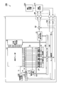
- FIG. 1 is a block diagram showing a schematic configuration of a solid-state imaging device according to a first embodiment of the present invention.
- the solid-state imaging device 1 shown in FIG. 1 includes a pixel array unit 10, a plurality of column AD (analog-digital) conversion circuits 20, a temperature AD conversion circuit 21, a pixel readout control unit 30, and horizontal readout control.
- Unit 40 timing generator 50, sensor control unit 60, digital signal processing unit 70, output circuit 80, interface unit 90, input circuit 100, reference voltage generation unit 110, bias generation unit 120, And a reference voltage generation unit 130.
- a plurality of pixels are arranged in a two-dimensional matrix.
- Each of the pixels arranged in the pixel array unit 10 includes, for example, a photoelectric conversion element such as a photodiode, and the photoelectric conversion element provided in each pixel has the amount of light incident within a certain accumulation time (exposure time) Generate a photoelectric conversion signal according to Then, the pixel array unit 10, under the control of readout from the pixel readout control unit 30, for each row of pixels arranged in the pixel array unit 10, a pixel signal corresponding to the photoelectric conversion signal generated by each pixel. The data is output to the corresponding column AD conversion circuit 20.
- the pixel readout control unit 30 generates an exposure signal for causing each of the pixels arranged in the pixel array unit 10 to perform exposure in accordance with the control timing signal output from the timing generator 50. Then, the pixel readout control unit 30 outputs the generated exposure signal to each pixel disposed in the pixel array unit 10 to perform exposure. In addition, the pixel read control unit 30 generates a read control signal for reading a pixel signal from each pixel arranged in the pixel array unit 10 according to the control timing signal output from the timing generator 50. Then, the pixel readout control unit 30 outputs the generated readout control signal for each row of the pixel array unit 10, and causes the column AD conversion circuit 20 to output the pixel signal of the pixel arranged in each row.
- the reference voltage generation unit 110 generates a reference voltage Vr for operating each component provided in the solid-state imaging device 1 and a temperature detection voltage Vt for detecting the temperature of the solid-state imaging device 1 (semiconductor substrate). Do.
- the reference voltage generation unit 110 is configured by a band gap reference circuit using a bipolar transistor. With this configuration, in the reference voltage generation unit 110, each of the reference voltage Vr having a temperature value of substantially zero and the temperature detection voltage Vt of a voltage value having a temperature coefficient corresponding to the temperature of the solid-state imaging device 1 , With a small circuit scale.
- the reference voltage generation unit 110 since the temperature detection voltage Vt generated by the reference voltage generation unit 110 is a voltage having a temperature coefficient according to the temperature of the solid-state imaging device 1 as described above, the role of the temperature signal output by the temperature sensor Is responsible for That is, the reference voltage generation unit 110 also has the function of a temperature sensor.
- the reference voltage generation unit 110 outputs (supplys) each of the generated reference voltage Vr and the temperature detection voltage Vt to the corresponding component. More specifically, the reference voltage generation unit 110 outputs the generated reference voltage Vr to the bias generation unit 120. Further, the reference voltage generation unit 110 outputs the generated temperature detection voltage Vt to the temperature AD conversion circuit 21.
- the bias generation unit 120 generates a bias voltage Vb for operating each component provided in the solid-state imaging device 1. More specifically, the bias generation unit 120 generates a bias voltage Vb of a voltage value according to the control signal output from the sensor control unit 60 from the reference voltage Vr output from the reference voltage generation unit 110. The bias generation unit 120 outputs the generated bias voltage Vb to each of the column AD conversion circuit 20, the temperature AD conversion circuit 21, the output circuit 80, and the reference voltage generation unit 130.
- the reference voltage generation unit 130 is output from the bias generation unit 120 which is referred to when each of the column AD conversion circuit 20 and the temperature AD conversion circuit 21 performs analog-digital conversion according to the control timing signal output from the timing generator 50. Generates a reference voltage based on the bias voltage Vb. It is to be noted that the reference voltage generated by the reference voltage generation unit 130 is the bias voltage Vb at a constant ratio to time from the timing when each of the column AD conversion circuit 20 and the temperature AD conversion circuit 21 starts analog-to-digital conversion. It is an analog voltage signal in which a voltage value monotonously changes (decreases or increases), that is, a so-called voltage signal of a ramp waveform. The reference voltage generation unit 130 outputs the generated reference voltage to each of the column AD conversion circuit 20 and the temperature AD conversion circuit 21.
- the solid-state imaging device 1 shown in FIG. 1 has a configuration in which one bias generation unit 120 and one reference voltage generation unit 130 common to all the column AD conversion circuits 20 and the temperature AD conversion circuits 21 are provided. ing.
- the column AD conversion circuit 20 is an AD conversion circuit that analog-digital converts a pixel signal (analog signal) output from the pixel of the corresponding column arranged in the pixel array unit 10.
- the column AD conversion circuit 20 generates a pixel signal based on the bias voltage Vb output from the bias generation unit 120, the reference voltage output from the reference voltage generation unit 130, and the control timing signal output from the timing generator 50. Analog to digital conversion. That is, the column AD conversion circuit 20 is generated from the reference voltage Vr whose temperature coefficient to the temperature of the solid-state imaging device 1 is almost zero (the degree of dependence on temperature is very small and can be said to be independent of temperature).
- the pixel signal is analog-digital converted in a stable state by analog-digital conversion based on the bias voltage Vb and the reference voltage.
- a plurality of column AD conversion circuits 20 are provided as many as the number of pixel columns arranged in the pixel array unit 10.
- Each column AD conversion circuit 20 converts digital data (parallel digital data) of a digital value corresponding to the size of the pixel signal analog-digital converted according to read control from the horizontal read control unit 40 into the digital signal processing unit 70.
- each of the column AD conversion circuits 20 sequentially sends parallel digital data (hereinafter referred to as “pixel data”) representing the amount of light exposed by each pixel arranged in the pixel array unit 10 to the digital signal processing unit 70. Output.
- the temperature AD conversion circuit 21 is an AD conversion circuit having the same configuration as that of the column AD conversion circuit 20. However, the temperature AD conversion circuit 21 changes the temperature detection voltage Vt (analog voltage) output from the reference voltage generation unit 110 to the temperature of the solid-state imaging device 1 instead of the pixel signal that the column AD conversion circuit 20 performs analog-to-digital conversion. Is analog-to-digital converted as a detected temperature signal. Similar to the column AD conversion circuit 20, the temperature AD conversion circuit 21 controls the bias voltage Vb output from the bias generation unit 120, the reference voltage output from the reference voltage generation unit 130, and the control output from the timing generator 50. The temperature detection voltage Vt is analog-digital converted based on the timing signal.
- Vt analog voltage
- the temperature AD conversion circuit 21 also has the temperature detection voltage Vt in a stable state based on the reference voltage Vr which does not depend on the temperature of the solid-state imaging device 1 (the temperature coefficient is almost zero). Analog to digital conversion.
- the temperature AD conversion circuit 21 converts digital data (parallel digital data) of a digital value corresponding to the magnitude of the temperature detection voltage Vt that has been analog-to-digital converted according to read control from the horizontal read control unit 40 into the digital signal processing unit 70. Output to That is, the temperature AD conversion circuit 21 converts parallel digital data (hereinafter referred to as "temperature data") representing the temperature of the solid-state imaging device 1 represented by the temperature detection voltage Vt output by the reference voltage generation unit 110 into a digital signal. It is output to the processing unit 70.
- temperature data parallel digital data
- the timing generator 50 generates a control timing signal that controls the timing at which each component provided in the solid-state imaging device 1 operates in accordance with control from the sensor control unit 60.
- the timing generator 50 outputs the generated control timing signal to each component provided in the solid-state imaging device 1. More specifically, the timing generator 50 includes a column AD conversion circuit 20 provided in the solid-state imaging device 1, a temperature AD conversion circuit 21, a pixel readout control unit 30, a horizontal readout control unit 40, and a digital signal processing unit.
- a control timing signal for controlling the timing at which each of the reference voltage generation unit 70 and the reference voltage generation unit 130 operate is generated and output.
- the timing generator 50 exposes incident light to each pixel arranged in the pixel array unit 10 to generate a photoelectric conversion signal, and reads the generated photoelectric conversion signal as a pixel signal.
- a control timing signal for controlling the timing is output to the pixel readout control unit 30.
- the pixel readout control unit 30 exposes each pixel disposed in the pixel array unit 10 when a control timing signal representing a timing of generating incident light and generating a photoelectric conversion signal is input from the timing generator 50. Exposure signals are output to the respective pixels to perform exposure.
- the control timing signal representing the timing of reading the pixel signal from each pixel arranged in the pixel array unit 10 is input from the timing generator 50
- the pixel read control unit 30 reads the pixel signal from each pixel.
- the readout control signal for each pixel is output for each row of the pixel array unit 10, and the pixel signal is output to each pixel arranged in the pixel array unit 10.
- the timing generator 50 is a control timing signal for controlling the timing at which each of the column AD conversion circuit 20 and the temperature AD conversion circuit 21 starts analog-to-digital conversion and the reference timing at the time of analog-to-digital conversion.
- the reference voltage generation unit 130, the column AD conversion circuit 20, and the temperature AD conversion circuit 21 are respectively output.
- the reference voltage generation unit 130 starts generation of a reference voltage when a control timing signal representing a timing at which each of the column AD conversion circuit 20 and the temperature AD conversion circuit 21 starts analog-to-digital conversion is input from the timing generator 50.
- the generated reference voltage is output to each of the column AD conversion circuit 20 and the temperature AD conversion circuit 21.
- each of the column AD conversion circuit 20 and the temperature AD conversion circuit 21 receives from the timing generator 50 a control timing signal representing the timing of starting analog-to-digital conversion, it starts analog-to-digital conversion and performs analog-to-digital conversion.
- the analog-to-digital conversion of the input signal (pixel signal or temperature detection voltage Vt) of the input analog-to-digital conversion is performed based on the control timing signal indicating the timing of the reference.
- the timing generator 50 outputs, to the horizontal read control unit 40, a control timing signal for controlling the timing of reading digital data analog-digital converted by each of the column AD conversion circuit 20 and the temperature AD conversion circuit 21. Further, the timing generator 50 controls a control timing signal for controlling the timing at which digital data sequentially read out from each of the column AD conversion circuit 20 and the temperature AD conversion circuit 21 by the horizontal read control unit 40 is processed. , And output to the digital signal processing unit 70.
- the horizontal read control unit 40 performs digital data (pixel data) obtained by analog-to-digital conversion of each of the column AD conversion circuits 20 according to the control timing signal output from the timing generator 50, and digital obtained by the analog-to-digital conversion of the temperature AD conversion circuit 21. A read control signal for reading data (temperature data) is generated. The horizontal read control unit 40 outputs the generated read control signal to each of the column AD conversion circuit 20 and the temperature AD conversion circuit 21, and digital data obtained by analog to digital conversion of each AD conversion circuit is sequentially sent to the digital signal processing unit 70. Make it output.
- the digital signal processing unit 70 controls digital data sequentially output from each of the column AD conversion circuit 20 and the temperature AD conversion circuit 21 under the control of the horizontal read control unit 40 in accordance with the control timing signal output from the timing generator 50. Perform predetermined digital data processing. That is, the digital signal processing unit 70 performs digital data processing on digital data (pixel data) analog-to-digital converted by each of the column AD conversion circuits 20 and digital data (temperature data) analog-to-digital converted by the temperature AD conversion circuit 21. Perform digital data processing.
- serial digital data For digital data processing performed by the digital signal processing unit 70, parallel digital data output from each of the column AD conversion circuit 20 and the temperature AD conversion circuit 21, that is, digital data configured by data of a plurality of bits, It includes digital data composed of 1-bit data, that is, digital data processing such as serialization processing for converting into serial digital data.
- the digital signal processing unit 70 outputs digital data (serial digital data) after digital data processing to the output circuit 80.
- the digital signal processing unit 70 performs various digital data processing besides serialization processing of parallel digital data output from each of the column AD conversion circuit 20 and the temperature AD conversion circuit 21 described above. For example, the digital signal processing unit 70 converts (returns) serial digital data converted by serialization into parallel digital data again, that is, outputs from each of the column AD conversion circuit 20 and the temperature AD conversion circuit 21. Digital data processing is performed to generate a clock signal, a synchronization signal, and the like necessary for performing processing for restoring the parallel digital data.
- the output circuit 80 is a differential buffer circuit that converts digital data (serial digital data) output from the digital signal processing unit 70 into a differential signal based on the bias voltage Vb output from the bias generation unit 120. .
- the output circuit 80 outputs each of the converted differential signals to the outside of the solid-state imaging device 1 through the corresponding interface unit 90.
- the output circuit 80 converts serial digital data output from the digital signal processing unit 70 into, for example, a differential signal compatible with a differential interface system such as a low voltage differential signaling (LVDS) system.
- LVDS low voltage differential signaling
- the output circuit 80 is serialized by the digital signal processing unit 70 with an LVDS differential signal (hereinafter referred to as “pixel data signal”) corresponding to pixel data serialized by the digital signal processing unit 70.
- the output circuit 80 converts into each of the differential signals of the LVDS system (hereinafter referred to as “temperature data signal”) corresponding to the temperature data. Then, the output circuit 80 outputs each of the converted LVDS differential signals to the outside of the solid-state imaging device 1 through the corresponding interface unit 90. The output circuit 80 also performs LVDS type termination processing and the like.
- the interface unit 90 is a terminal for connecting the solid-state imaging device 1 to the outside.
- the interface unit 90 is shown having a configuration with one input terminal.
- the size (projection area) of the semiconductor substrate forming the solid-state imaging device 1 is reduced by sharing the output terminal of the pixel data signal and the output terminal of the temperature data signal. .
- the input circuit 100 is a buffer circuit for transmitting a signal input from the outside of the solid-state imaging device 1 to the sensor control unit 60.
- the solid-state imaging device 1 shown in FIG. 1 shows an input circuit 100 having a configuration including two buffer circuits corresponding to each of two input terminals.
- the input circuit 100 outputs each signal input from the outside of the solid-state imaging device 1 through the corresponding interface unit 90 to the sensor control unit 60.
- a component for example, a command signal or a setting signal
- I2C serial communication is input to the input circuit 100 from the outside of the solid-state imaging device 1 through the corresponding interface unit 90.
- the input circuit 100 outputs each signal of the input I2C serial communication to the sensor control unit 60.
- the sensor control unit 60 controls the overall operation of the solid-state imaging device 1 in accordance with a signal input from the outside of the solid-state imaging device 1.
- the sensor control unit 60 outputs a control signal for controlling the operation of each component provided in the solid-state imaging device 1 to each component. More specifically, the sensor control unit 60 controls the operation of each of the timing generator 50 and the bias generation unit 120 provided in the solid-state imaging device 1 according to a signal input from the outside of the solid-state imaging device 1. Output a control signal for
- the control signal that the sensor control unit 60 outputs to the timing generator 50 is a control signal for controlling the imaging operation in the solid-state imaging device 1. More specifically, when a command signal instructing imaging by the solid-state imaging device 1 is input from the outside of the solid-state imaging device 1 via the input terminal of the interface unit 90 and the input circuit 100, the sensor control unit 60 outputs, to the timing generator 50, a control signal indicating that an imaging operation is to be performed. Thus, the timing generator 50 outputs, to the pixel readout control unit 30, control timing signals for controlling the timing of exposure and readout of pixel signals by the respective pixels arranged in the pixel array unit 10.
- the timing generator 50 outputs control timing signals for analog-to-digital conversion of pixel signals (analog signals) output from the pixel array unit 10 to the reference voltage generation unit 130 and the column AD conversion circuit 20, respectively. . Further, the timing generator 50 outputs, to the horizontal read control unit 40, a control timing signal for controlling the read timing of pixel data analog-to-digital converted by each of the column AD conversion circuits 20. Further, the timing generator 50 is a digital signal that is a control timing signal for controlling the timing of digital data processing (serialization processing) of pixel data sequentially read from each of the column AD conversion circuits 20 by the horizontal read control unit 40. It is output to the processing unit 70.
- the solid-state imaging device 1 receives the exposure amount of each pixel disposed in the pixel array unit 10 via the output circuit 80 and the output terminal of the interface unit 90. A corresponding pixel data signal is output to the outside of the solid-state imaging device 1.
- the control signal output from the sensor control unit 60 to the timing generator 50 is a control signal for controlling the temperature detection operation in the solid-state imaging device 1. More specifically, when a command signal instructing to detect the temperature of the solid-state imaging device 1 is input from the outside of the solid-state imaging device 1 via the input terminal of the interface unit 90 and the input circuit 100, sensor control The unit 60 outputs a control signal representing that the temperature detection operation is performed to the timing generator 50.
- the timing generator 50 converts a control timing signal for converting the temperature detection voltage Vt (analog voltage) output from the reference voltage generation unit 110 into an analog to digital signal, the reference voltage generation unit 130 and the temperature AD conversion circuit 21. Output to each of.
- the timing generator 50 outputs, to the horizontal read control unit 40, a control timing signal for controlling the read timing of temperature data analog-digital converted by the temperature AD conversion circuit 21. Further, the timing generator 50 controls the digital signal processing unit 70 to control timing for digital data processing (serialization processing) of the temperature data read from the temperature AD conversion circuit 21 by the horizontal reading control unit 40. Output to The solid-state imaging device 1 controls the temperature of each component by the timing generator 50 so that the temperature of the solid-state imaging device 1 output from the reference voltage generation unit 110 via the output circuit 80 and the output terminal of the interface unit 90. The voltage value of the temperature detection voltage Vt having the temperature coefficient corresponding to the temperature data signal representing the current temperature of the solid-state imaging device 1 is output to the outside of the solid-state imaging device 1.
- the sensor control unit 60 has both a command signal instructing to perform imaging by the solid-state imaging device 1 and a command signal instructing to detect the temperature of the solid-state imaging device 1 from outside the solid-state imaging device 1 Even when it is input, according to the control signal output to the timing generator 50, a pixel data signal according to the exposure amount of each pixel arranged in the pixel array unit 10 and a temperature representing the current temperature of the solid-state imaging device 1 Each of the data signals can be output to the outside of the solid-state imaging device 1.
- the sensor control unit 60 performs analog-to-digital conversion of the temperature detection voltage Vt output from the reference voltage generation unit 110 simultaneously with analog-to-digital conversion of the pixel signals of the respective rows output from the pixel array unit 10 Control signal to the timing generator 50. Further, the sensor control unit 60 controls a control signal for performing control so that the temperature AD conversion circuit 21 reads out analog-digital converted temperature data subsequently to reading of pixel data that each of the column AD conversion circuits 20 performs analog-to-digital conversion. Output to the generator 50.
- the solid-state imaging device 1 continues to the pixel data signal output for each row of pixels arranged in the pixel array unit 10 by using the temperature data signal representing the current temperature of the solid-state imaging device 1 as the solid-state imaging device 1 It can be output to the outside. That is, the solid-state imaging device 1 outputs temperature data every period (so-called horizontal period) from when the pixel data signal of a certain row of the pixel array unit 10 is output until the pixel data signal of the next row is output. A signal can be output to the outside of the solid-state imaging device 1.
- the control signal output from the sensor control unit 60 to the bias generation unit 120 is a control signal for controlling the voltage value of the bias voltage Vb generated by the bias generation unit 120. More specifically, when the setting signal representing the setting and setting value of bias voltage Vb in solid-state imaging device 1 is input from the outside of solid-state imaging device 1 via the input terminal of interface unit 90 and input circuit 100, The sensor control unit 60 outputs, to the bias generation unit 120, a control signal indicating that the operation of setting the voltage value of the bias voltage Vb to the input set value is performed. Thereby, the bias generation unit 120 generates the bias voltage Vb of the voltage value according to the set value input from the sensor control unit 60 based on the reference voltage Vr output from the reference voltage generation unit 110. The bias voltage Vb is output to each component.
- Each component operates based on the bias voltage Vb output from the bias generation unit 120. That is, each of the column AD conversion circuit 20, the temperature AD conversion circuit 21, the output circuit 80, and the reference voltage generation unit 130 provided in the solid-state imaging device 1 uses the bias voltage Vb output from the bias generation unit 120. Based on the operation of the above-described imaging and temperature detection. Thereby, the solid-state imaging device 1 outputs a pixel data signal and a temperature data signal based on the bias voltage Vb of the voltage value set from the outside to the outside of the solid-state imaging device 1.
- the reference voltage Vr does not depend on the temperature of the solid-state imaging device 1 (it is not affected by the temperature of the solid-state imaging device 1).
- a reference voltage generation unit 110 that generates a temperature detection voltage Vt of a voltage value (having a temperature coefficient corresponding to the temperature) that changes according to the temperature of the solid-state imaging device 1.
- the column AD conversion circuit 20, the output circuit 80, and the reference voltage are generated based on the bias voltage Vb generated based on the reference voltage Vr generated by the reference voltage generation unit 110.
- Each of the generation units 130 operates. Thereby, in the solid-state imaging device 1 of the first embodiment, it is possible to output a pixel data signal in a state in which the influence of the temperature of the solid-state imaging device 1 is small, that is, the degree of dependence on the temperature is small.
- the solid-state imaging device 1 includes the temperature AD conversion circuit 21 having the same configuration as the column AD conversion circuit 20 that performs analog-to-digital conversion on the voltage value of the temperature detection voltage Vt generated by the reference voltage generation unit 110. .
- the temperature of the solid-state imaging device 1 can be detected based on the voltage value of the temperature detection voltage Vt generated by the reference voltage generation unit 110.
- the temperature AD conversion circuit 21 also operates based on the bias voltage Vb generated based on the reference voltage Vr generated by the reference voltage generation unit 110.
- the solid-state imaging device 1 of the first embodiment it is possible to output a temperature data signal in a state in which the influence of the temperature of the solid-state imaging device 1 is small, that is, the degree of dependence on the temperature is small.
- the temperature of the solid-state imaging device 1 semiconductor substrate represented by the voltage value of the temperature detection voltage Vt An accurate represented temperature data signal can be output.
- the temperature of the solid-state imaging device 1 largely fluctuates to the high temperature side, and pixels from each pixel arranged in the pixel array unit 10 due to the influence of dark current Even if the signal is not normally output to the corresponding column AD conversion circuit 20, the bias voltage Vb or the reference voltage of the column AD conversion circuit 20, the output circuit 80, based on the reference voltage Vr whose voltage value is substantially zero.
- the bias voltage Vb of the column AD conversion circuit 20 and the output circuit 80 can operate properly without being greatly affected by the temperature of the solid-state imaging device 1.
- the output circuit 80 is a circuit element that operates at high speed to convert serial digital data into a differential signal and output it, and is a circuit element that is more susceptible to bias fluctuation due to temperature fluctuation. .
- the output circuit 80 can determine the current value of the differential signal to be output based on the bias voltage Vb generated by the bias generation unit 120 based on the reference voltage Vr. For this reason, in the solid-state imaging device 1 according to the first embodiment, it is possible to suppress the fluctuation of the current value due to the bias fluctuation which occurs when the temperature fluctuates, and maintain the output capability of the signal in the output circuit 80.
- the output circuit 80 is a temperature data signal that accurately represents the temperature of the solid-state imaging device 1 represented by the voltage value of the temperature detection voltage Vt in a wider temperature range. Can be output to the outside of the solid-state imaging device 1.
- the output circuit 80 can output a temperature data signal representing an accurate temperature in a wider range than in the past, for example, up to 125 ° C.
- the output circuit 80 outputs a temperature data signal accurately representing the temperature (for example, 125 ° C.) of the solid-state imaging device 1 that can be represented by the voltage value of the temperature detection voltage Vt generated by the reference voltage generation unit 110. be able to.
- the output circuit 80 outputs a temperature data signal accurately representing the temperature (for example, 125 ° C.) of the solid-state imaging device 1 that can be represented by the voltage value of the temperature detection voltage Vt generated by the reference voltage generation unit 110.
- the same components as those for outputting pixel data signals that is, the temperature via the digital signal processing unit 70, the output circuit 80, and the interface unit 90.
- Output data signal that is, in the solid-state imaging device 1 according to the first embodiment, the component for outputting the pixel data signal and the component for outputting the temperature data signal are shared.
- the solid-state imaging device can be provided without separately providing a component (circuit element) for outputting a temperature data signal representing the detected temperature to the outside of the solid-state imaging device 1 The increase of the circuit scale of 1 can be reduced.
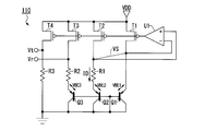
- FIG. 2 is a circuit diagram showing an example of the configuration of the reference voltage generation unit 110 provided in the solid-state imaging device 1 according to the first embodiment of the present invention.
- the reference voltage generation unit 110 shown in FIG. 2 includes three bipolar transistors Q1 to Q3, three resistors R1 to R3, and four field effect transistors (FETs) T1 to T4. And an operational amplifier U1.
- the inverting input terminal of the operational amplifier U1 is connected to the emitter terminal of the bipolar transistor Q1 and one of the drain terminal and the source terminal of the field effect transistor T1.
- the noninverting input terminal of the operational amplifier U1 is connected to the first terminal of the resistor R1 and one of the drain terminal and the source terminal of the field effect transistor T2.
- the second terminal of the resistor R1 is connected to the emitter terminal of the bipolar transistor Q2.
- the output terminal of the operational amplifier U1 is connected to the gate terminal of the field effect transistor T1, the gate terminal of the field effect transistor T2, the gate terminal of the field effect transistor T3, and the gate terminal of the field effect transistor T4.
- One terminal of the source terminal and drain terminal of the field effect transistor T1, one terminal of the source terminal and drain terminal of the field effect transistor T2, one terminal of the source terminal and drain terminal of the field effect transistor T3, and the field effect One terminal of the source terminal and the drain terminal of the transistor T4 is connected to the power supply VDD.
- One terminal of the drain terminal and the source terminal of the field effect transistor T3 is connected to the first terminal of the resistor R2 and serves as an output terminal of the reference voltage Vr in the reference voltage generation unit 110.
- the second terminal of the resistor R2 is connected to the emitter terminal of the bipolar transistor Q3.
- One terminal of the drain terminal and the source terminal of the field effect transistor T4 is connected to the first terminal of the resistor R3 and serves as an output terminal of the temperature detection voltage Vt in the reference voltage generation unit 110.
- the second terminal of the resistor R3, the collector and base terminals of the bipolar transistor Q1, the collector and base terminals of the bipolar transistor Q2, and the collector and base terminals of the bipolar transistor Q3 are grounded.
- the potential of the first terminal of the resistor R1 is a virtual short circuit between the inverting input terminal and the non-inverting input terminal of the operational amplifier U1 Short circuit) VS results in the potential VBE1 between the base terminal and the emitter terminal of the bipolar transistor Q1.
- the potential of the second terminal of the resistor R1 becomes the potential VBE2 between the base terminal and the emitter terminal of the bipolar transistor Q2.
- the current ID flowing through the resistor R1 is expressed by the following equation (1).
- R1 is the resistance value of the resistor R1.
- k is the Boltzmann constant
- T is the absolute temperature
- q is the charge of the electron.
- ln (n) represents the ratio of the bipolar transistor Q1 to the bipolar transistor Q2.
- the ratio ln (n) between the bipolar transistor Q1 and the bipolar transistor Q2 has a positive temperature coefficient.
- the current ID represented by the above equation (1) is a resistance R2 due to the field effect transistor T1, the field effect transistor T2, the field effect transistor T3 and the field effect transistor T4. And also flows through resistor R3. From this, the temperature detection voltage Vt which is a potential of the first terminal of the resistor R3 is expressed as the following equation (2).
- Vt R3 / R1 * (kT / q * ln (n)) (2)
- R3 is the resistance value of the resistor R3.
- the temperature detection voltage Vt has a positive temperature coefficient, and is a temperature-dependent voltage, that is, a temperature-dependent voltage.
- the reference voltage Vr which is the potential of the first terminal of the resistor R2
- the potential VBE3 between the base terminal and the emitter terminal of the bipolar transistor Q3 because the potential of the second terminal of the resistor R2 becomes It is expressed as (3).
- Vr VBE3 + R2 / R1 * (kT / q * ln (n)) ... (3)
- R2 is the resistance value of the resistor R2.
- the potential VBE3 of the first term of the right side of the above equation (3) has a negative temperature coefficient. Therefore, in the above equation (3), the temperature detection voltage Vt is the potential VBE3 of the first term of the right side having a negative temperature coefficient, and R2 / R1 * (kT) of the second term of the right side having a positive temperature coefficient. With / q * ln (n)), the voltage does not depend on temperature, that is, does not change with temperature.
- the resistance also has temperature characteristics.
- the voltage values of the temperature detection voltage Vt and the reference voltage Vr to be output are determined by the ratio of the resistances, so that the temperature characteristics of the respective resistances are obtained.
- the configuration is not affected. More specifically, the voltage value of the temperature detection voltage Vt is determined by the ratio R3 / R1 of the resistance values on the right side of the above equation (2), and the voltage value of the reference voltage Vr is on the right side of the above equation (3) It is set as a structure which becomes settled by ratio R2 / R1 of resistance value of 2 terms.
- the voltage value does not change according to the temperature for operating the respective components provided in the solid-state imaging device 1 based on the power supply VDD.
- a temperature detection voltage Vt (having a temperature coefficient) whose voltage value changes according to the temperature for detecting the reference voltage Vr (the temperature coefficient is almost zero) and the temperature of the solid-state imaging device 1 (semiconductor substrate) Generate and output each of.
- the specific circuit configuration of the reference voltage generation unit 110 is not limited to the circuit configuration of the reference voltage generation unit 110 shown in FIG. That is, in the circuit configuration of the reference voltage generation unit 110, the voltage value does not change with temperature (the temperature coefficient is almost zero), and the voltage value changes with temperature (with the temperature coefficient Any circuit configuration may be used as long as it can generate and output each of the temperature detection voltages Vt.
- FIG. 3 is a circuit diagram showing an example of the configuration of the output circuit 80 provided in the solid-state imaging device 1 according to the first embodiment of the present invention.
- the output circuit 80 shown in FIG. 3 is composed of two logical NOT circuits INV1 and logical NOT circuits INV2, four switches SW1 to SW4, and a current source CS.
- serial digital data output from the digital signal processing unit 70 is input to the input terminal of the logical NOT circuit INV1, and the output terminal is the input terminal of the logical NOT circuit INV2. It is connected to the control terminal of the switch SW2 and the control terminal of the switch SW3.
- the output terminal of the logical NOT circuit INV2 is connected to the control terminal of the switch SW1 and the control terminal of the switch SW4.
- the first terminal of the switch SW1 and the first terminal of the switch SW3 are connected to the output terminal of the current source CS.
- the input terminal of the current source CS is connected to the power supply VDD, and the bias voltage Vb output from the bias generation unit 120 is input to the bias terminal.
- the second terminal of the switch SW1 is connected to the first terminal of the switch SW2, and serves as a first output terminal of a differential signal in the output circuit 80 (for example, an output terminal of a differential positive signal).
- the second terminal of the switch SW3 is connected to the first terminal of the switch SW4, and serves as a second output terminal of the differential signal in the output circuit 80 (for example, an output terminal of a differential negative signal).
- the second terminal of the switch SW2 and the second terminal of the switch SW4 are grounded.
- the output circuit 80 shown in FIG. 3 outputs a differential signal representing the input serial digital data from each of the first output terminal and the second output terminal. More specifically, the output circuit 80 outputs a differential signal (for example, a differential positive signal) representing the input serial digital data from the first output terminal, and digitalizes the input serial digital data. A differential signal (for example, a differential negative signal) representing digital data whose value is inverted is output from the second output terminal.
- the current value of the differential signal output from the output circuit 80 from each of the first output terminal and the second output terminal is determined by the current source CS according to the bias voltage Vb output from the bias generation unit 120. It is a defined current value.
- each differential signal output from the output circuit 80 is a differential signal in a state in which the fluctuation of the current value due to the bias fluctuation that occurs when the temperature fluctuates. Then, each differential signal output from the output circuit 80 is solid through the corresponding interface unit 90, more specifically, an output terminal that doubles as an output of a pixel data signal and a temperature data signal in the interface unit 90. The image is output to the outside of the imaging device 1.
- the specific circuit configuration of the output circuit 80 is not limited to the circuit configuration of the output circuit 80 shown in FIG. That is, the circuit configuration of the output circuit 80 may be any circuit configuration as long as it can output the input serial digital data as a differential signal of the current value determined by the bias voltage Vb. .
- a pixel array unit (pixel array unit 10) in which a plurality of pixels that output photoelectric conversion signals according to the amount of incident light are arranged in a matrix, and a temperature that changes according to a change in temperature
- a reference voltage generation unit (reference voltage generation unit 110) that generates a detection voltage (temperature detection voltage Vt) and a reference voltage (reference voltage Vr) that does not depend on a change in temperature, and a photoelectric conversion signal output from the pixel array unit 10.
- the temperature detection voltage Vt generated by the reference voltage generation unit 110 by signal processing and reading out (the column AD conversion circuit 20, the temperature AD conversion circuit 21, the pixel readout control unit 30, the horizontal readout control unit 40, An output unit (a digital signal that outputs both the reference voltage generation unit 130), the photoelectric conversion signal subjected to signal processing in the reading unit, and the temperature detection voltage Vt to the outside
- a bias generation unit (bias generation unit 120) for supplying a bias voltage (bias voltage Vb) generated based on the reference voltage Vr to the read unit and the output unit;
- a solid-state imaging device solid-state imaging device 1 is provided.
- the readout unit converts the input analog signal (pixel signal or temperature detection voltage Vt: temperature signal) into a digital signal and outputs the digital signal (column AD conversion circuit 20). And the temperature AD conversion circuit 21) are configured.
- the timing of reading out the photoelectric conversion signal from the pixel array unit 10 the timing of reading out the signal processing and signal processing by the reading unit and the timing of reading out the temperature detection voltage Vt
- the solid-state imaging device 1 is provided with a timing generator (timing generator 50) that controls
- the solid-state imaging device 1 including the sensor control unit (sensor control unit 60) that controls the timing generator 50 and the bias generation unit 120 is configured.
- FIG. 4 is a block diagram showing a schematic configuration of an imaging device equipped with the solid-state imaging device 1 according to the first embodiment of the present invention.
- the imaging device 200 illustrated in FIG. 4 includes the solid-state imaging device 1, an imaging control unit 210, and an exposure control device 220.
- the exposure control device 220 is a device for controlling the amount of light incident on the solid-state imaging device 1 under the control of the imaging control unit 210.
- the exposure control device 220 is, for example, a mechanical shutter, an aperture device, or the like when the imaging device 200 is a system of a digital single-lens reflex camera.
- the exposure control device 220 is, for example, a light source device such as a light emitting diode (LED) light source when the imaging device 200 is a system of an endoscope device.
- LED light emitting diode
- the configuration of the exposure control device 220 is not particularly defined.
- the imaging control unit 210 is a control unit that controls the setting and operation timing of each of the solid-state imaging device 1 and the exposure control device 220 when performing imaging in the imaging device 200.
- the imaging control unit 210 detects each of the solid-state imaging device 1 and the exposure control device 220 based on the pixel data signal that the solid-state imaging device 1 captures and outputs and the temperature data signal that the solid-state imaging device 1 detects and outputs. Control settings and operation timing. For example, the imaging control unit 210 outputs a control signal for causing the solid-state imaging device 1 to perform a temperature detection operation before capturing an image in the imaging device 200, and acquires a temperature data signal detected by the solid-state imaging device 1. Do.
- the imaging control unit 210 determines an imaging method in the solid-state imaging device 1 based on the acquired temperature data signal, and outputs a control signal for performing an imaging operation by the determined imaging method. Thereby, the imaging control unit 210 can acquire a pixel data signal on which the temperature detected by the solid-state imaging device 1 is reflected.
- FIG. 5 is a timing chart showing an example of signal read timing in the imaging device 200 equipped with the solid-state imaging device 1 according to the first embodiment of the present invention.
- each of the imaging control unit 210 is disposed in the pixel array unit 10 provided in the solid-state imaging device 1. It is a control timing in the case of periodically performing control of acquiring a temperature data signal during an exposure period in which light incident on a pixel is exposed and acquiring a pixel data signal after the exposure is completed.
- an exposure control signal for causing the imaging control unit 210 to expose light to the solid-state imaging device 1, and the imaging control unit 210 periodically each of a pixel data signal and a temperature data signal from the solid-state imaging device 1.
- Two output terminals (differential signals) in the interface unit 90 in which the solid-state imaging device 1 outputs the pixel data signal and the temperature data signal as the vertical synchronization signal VD and the horizontal synchronization signal HD which are used as a reference when acquiring And each one is shown.
- the timing chart shown in FIG. 5 shows respective signals in a period in which pixel data signals for one frame are acquired.
- the imaging control unit 210 outputs the vertical synchronization signal VD.
- the exposure control device 220 is controlled so that light enters the solid-state imaging device 1 in a period when the synchronized exposure control signal is at the “High” level. Further, at this time, the imaging control unit 210 instructs the two input terminals of the interface unit 90 of the solid-state imaging device 1 to perform imaging, for example, by I2C serial communication (hereinafter referred to as “imaging command” Output).
- the imaging command output from the imaging control unit 210 is input to the sensor control unit 60 via the input terminal of the interface unit 90 and the input circuit 100.
- the sensor control unit 60 outputs a control signal indicating that the exposure operation is to be performed to the timing generator 50 in accordance with the imaging command input from the imaging control unit 210.
- the timing generator 50 outputs, to the pixel readout control unit 30, a control timing signal for controlling the exposure timing of each pixel arranged in the pixel array unit 10.
- the pixel readout control unit 30 outputs an exposure control signal to each of the pixels arranged in the pixel array unit 10 to expose the incident light.
- the imaging control unit 210 selects a pixel according to the pixel signal output from each pixel at timing synchronized with the horizontal synchronization signal HD.
- a command signal (hereinafter referred to as a “pixel read command”) instructing reading of a data signal for each row of the pixel array unit 10 is, for example, two input terminals of the interface unit 90 of the solid-state imaging device 1 by I2C serial communication. Output to Thus, in the solid-state imaging device 1, the pixel read command output from the imaging control unit 210 is input to the sensor control unit 60 via the input terminal of the interface unit 90 and the input circuit 100.
- the sensor control unit 60 outputs, to the timing generator 50, a control signal indicating that the operation of reading the pixel signal is to be performed in accordance with the pixel read command input from the imaging control unit 210.
- the timing generator 50 outputs, to the pixel readout control unit 30, a control timing signal for controlling the timing at which the pixel signal is read out from each of the pixels arranged in the pixel array unit 10.
- the pixel readout control unit 30 outputs a readout control signal for each row of each pixel arranged in the pixel array unit 10 to output a pixel signal.
- the timing generator 50 outputs a control timing signal for controlling the timing of starting analog-digital conversion of the pixel signal output from each pixel to each of the reference voltage generation unit 130 and the column AD conversion circuit 20.
- the reference voltage generation unit 130 outputs the reference voltage
- the column AD conversion circuit 20 generates the bias voltage Vb output from the bias generation unit 120 and the reference voltage output from the reference voltage generation unit 130.
- the pixel signal output from the pixel of the corresponding column is analog-digital converted.
- the timing generator 50 outputs, to the horizontal readout control unit 40, a control timing signal for controlling the timing at which each of the column AD conversion circuits 20 reads out the pixel data converted from analog to digital.
- the horizontal read control unit 40 sequentially reads pixel data analog-to-digital converted by each column AD conversion circuit 20 and outputs the pixel data to the digital signal processing unit 70.
- the timing generator 50 outputs, to the digital signal processing unit 70, a control timing signal for controlling the timing of digital data processing of pixel data (parallel digital data) sequentially read by the horizontal read control unit 40.
- the digital signal processing unit 70 outputs serial digital data after digital data processing (serialization processing) on sequentially input pixel data to the output circuit 80.
- the output circuit 80 outputs a pixel data signal corresponding to serial digital data output from the digital signal processing unit 70 to the imaging control unit 210 outside the solid-state imaging device 1 through the output terminal of the interface unit 90.
- a command signal (hereinafter referred to as “temperature read command”) instructing detection of temperature is, for example, I2C serial. It outputs to two input terminals of the interface part 90 of the solid-state image sensor 1 by communication.
- the temperature reading command output from the imaging control unit 210 is input to the sensor control unit 60 via the input terminal of the interface unit 90 and the input circuit 100.
- the sensor control unit 60 outputs a control signal indicating that the temperature detection operation is to be performed to the timing generator 50 in response to the temperature read command input from the imaging control unit 210.
- the timing generator 50 controls the control timing signal for controlling the timing of starting the analog-to-digital conversion of the temperature detection voltage Vt output from the reference voltage generation unit 110, the reference voltage generation unit 130, and the temperature AD conversion circuit. Output to each of 21.
- the reference voltage generation unit 130 outputs the reference voltage
- the temperature AD conversion circuit 21 is based on the bias voltage Vb output from the bias generation unit 120 and the reference voltage output from the reference voltage generation unit 130.
- the temperature detection voltage Vt output from the reference voltage generation unit 110 is analog-digital converted.
- the timing generator 50 outputs, to the horizontal read control unit 40, a control timing signal for controlling the timing at which the temperature AD conversion circuit 21 reads out the temperature data converted from analog to digital.
- the horizontal read control unit 40 reads out the temperature data analog-to-digital converted by the temperature AD conversion circuit 21 and causes the digital signal processing unit 70 to output the temperature data.
- the timing generator 50 outputs, to the digital signal processing unit 70, a control timing signal for controlling the timing of digital data processing of temperature data (parallel digital data) read by the horizontal read control unit 40.
- the digital signal processing unit 70 outputs serial digital data after digital data processing (serialization processing) on the input temperature data to the output circuit 80.
- the output circuit 80 outputs the temperature data signal corresponding to the serial digital data output from the digital signal processing unit 70 to the imaging control unit 210 outside the solid-state imaging device 1 through the output terminal of the interface unit 90.
- the imaging control unit 210 exposes each pixel arranged in the pixel array unit 10 at the timing of the exposure control signal synchronized with the vertical synchronization signal VD. Solid-state imaging so that pixel data signals corresponding to the pixel signals output from the respective pixels are read out for each row of the pixel array unit 10 from the timing synchronized with the horizontal synchronization signal HD after the end of the exposure period.
- the element 1 is controlled. Further, the imaging control unit 210 sets the temperature detection voltage Vt in a period in which the pixel data signal is not read out, and in a vertical blanking period in which the vertical synchronization signal VD does not read out the pixel data signal in the timing chart shown in FIG.
- the solid-state imaging device 1 is controlled so as to read out the temperature data signal detected based on it. Thereby, the imaging control unit 210 can acquire the temperature data signal detected in the solid-state imaging device 1 during the exposure period in which the acquisition of the pixel data signal from the solid-state imaging device 1 is not affected.
- the imaging control unit 210 may output a temperature readout command indicating detection of a temperature to the solid-state imaging device 1 multiple times during the vertical blanking period.
- the imaging control unit 210 can acquire temperature data signals for the number of times of the temperature reading command that has been output, that is, the number of samplings for temperature detection can be increased. It can be detected with high accuracy.
- the imaging control unit 210 is a solid-state imaging device 1.
- the temperature data signal acquired during the exposure period of each pixel disposed in the pixel array unit 10 provided in the solid-state imaging device 1 is a solid pixel data signal acquired after the exposure is completed.
- it can also be used to correct according to the temperature of the imaging device 1, it can also be used to change the setting of the solid-state imaging device 1 when acquiring a pixel data signal after the exposure is completed. That is, the imaging control unit 210 can also be used for feedback control to control an operation at the time of outputting a pixel data signal based on the temperature data signal acquired during the exposure period of each pixel.
- the imaging control unit 210 determines the voltage value of the bias voltage Vb based on the acquired temperature data signal, and sets the determined voltage value, whereby the column AD conversion circuit 20 generates a pixel signal as a pixel. It can be used for stabilization of conversion accuracy at the time of analog-to-digital conversion into data, and improvement of output capability when the output circuit 80 converts pixel data into differential signals and outputs.
- FIG. 6 is a timing chart showing another example of signal readout timing in the imaging device 200 equipped with the solid-state imaging device 1 according to the first embodiment of the present invention. Similar to the timing chart shown in FIG. 5, in the timing chart shown in FIG. 6, in the case where the imaging apparatus 200 is a system of an endoscope apparatus, for example, the imaging control unit 210 is provided in the solid-state imaging device 1. Based on the acquired temperature data signal, the temperature data signal is acquired during the exposure period of each of the pixels arranged in the pixel array unit 10, and before the pixel data signal is acquired after the exposure is completed, It is a control timing in the case of changing setting of 1.
- a vertical synchronization signal HD as a reference when cyclically acquiring each of the temperature data signal and the temperature data signal.
- two output terminals and an input terminal in the interface unit 90 are shown separately. More specifically, two output terminals (differential signals) in the interface unit 90 in which the solid-state imaging device 1 outputs each of the pixel data signal and the temperature data signal, and the imaging control unit 210 include Each of two input terminals (setting signals) in the interface unit 90 to be input to change the setting is shown. Note that the timing chart shown in FIG. 6 also shows the respective signals during a period in which pixel data signals for one frame are acquired, as in the timing chart shown in FIG.
- each command signal imaging command and pixel readout command
- the operation of each component in the solid-state imaging device 1 is the same as the operation described in the timing chart shown in FIG. Therefore, the detailed description regarding control of imaging by the imaging control unit 210 illustrated in the timing chart illustrated in FIG. 6 is omitted.
- the period in which the imaging control unit 210 outputs the respective command signals to the two input terminals of the interface unit 90 is a very short period. Therefore, the timing chart shown in FIG.
- the imaging control unit 210 does not show periods during which the imaging control unit 210 outputs command signals to the two input terminals of the interface unit 90. Further, in the timing chart shown in FIG. 6, while the solid-state imaging device 1 outputs a pixel data signal, the imaging control unit 210 does not control anything with respect to the solid-state imaging device 1; Since this is an unprocessed time in which no signal is output to the two input terminals, the period of this unprocessed time is shown as an idle (IDLE) period.
- IDLE idle
- the imaging control unit 210 when the imaging control unit 210 enters the vertical blanking period, a temperature read command instructing to detect a temperature is transmitted to the interface unit 90 of the solid-state imaging device 1 by I2C serial communication, for example. Output to the 2 input terminals of.
- the solid-state imaging device 1 operates in the same manner as the operation described in the timing chart shown in FIG. 5, and outputs the temperature data signal to the imaging control unit 210 via the output terminal of the interface unit 90. Note that, in consideration of the entire period of the timing chart illustrated in FIG. 6, the period in which the imaging control unit 210 outputs the temperature read command to the two input terminals of the interface unit 90 is a very short period. Therefore, the timing chart shown in FIG.
- the imaging control unit 210 does not show the period during which the imaging control unit 210 is outputting the temperature read command. Further, in the timing chart shown in FIG. 6, since the imaging control unit 210 does not control the solid-state imaging device 1 at all even while the solid-state imaging device 1 outputs the temperature data signal, it is an unprocessed time. The period of this unprocessed time is shown as an idle (IDLE) period.
- the setting signal representing the setting of the bias voltage Vb and the setting value is, for example, I2C. It outputs to two input terminals of the interface part 90 of the solid-state image sensor 1 by serial communication.
- the setting signal output from the imaging control unit 210 is input to the sensor control unit 60 via the input terminal of the interface unit 90 and the input circuit 100.
- the sensor control unit 60 outputs, to the bias generation unit 120, a control signal indicating that the operation of setting the voltage value of the bias voltage Vb is performed based on the setting signal input from the imaging control unit 210.
- the bias generation unit 120 changes the voltage value of the bias voltage Vb generated based on the reference voltage Vr output from the reference voltage generation unit 110 to the setting value output from the sensor control unit 60. Then, the bias generation unit 120 generates a bias voltage Vb of a voltage value according to the changed setting value thereafter to generate the column AD conversion circuit 20, the temperature AD conversion circuit 21, the output circuit 80, and the reference voltage generation. Output to each of the units 130.
- each of the column AD conversion circuit 20, the temperature AD conversion circuit 21, the output circuit 80, and the reference voltage generation unit 130 outputs the bias voltage Vb of the changed voltage value output from the bias generation unit 120. Based on the operation, it operates in the same manner as the operation described in the timing chart shown in FIG.
- each of the column AD conversion circuit 20, the temperature AD conversion circuit 21, the output circuit 80, and the reference voltage generation unit 130 picks up an image based on the bias voltage Vb of the voltage value set by the imaging control unit 210.
- the imaging and temperature detection operations are performed according to the control from the control unit 210, and the pixel data signal and the temperature data signal are output to the imaging control unit 210 outside the solid-state imaging device 1 through the output terminal of the interface unit 90. Do.
- the imaging control unit 210 controls the operation of each pixel disposed in the pixel array unit 10 before acquiring the pixel data signal from the solid-state imaging device 1.
- a temperature data signal during an exposure period is acquired.
- the imaging control unit 210 changes the voltage value of the bias voltage Vb to control the operation when the solid-state imaging device 1 outputs the pixel data signal and the temperature data signal. I do.
- the imaging control unit 210 acquires a pixel data signal and a temperature data signal based on the feedback voltage controlled bias voltage Vb, that is, a pixel data signal and a temperature data signal which are not influenced by the temperature of the solid-state imaging device 1.
- the frequency of the pixel data signal and the temperature data signal to be output is serialized because serial digital data of the parallel digital data output from each AD conversion circuit is converted to analog digital data and output. It is conceivable that the bit error rate at the time when the imaging control unit 210 acquires a pixel data signal or a temperature data signal is increased due to the blunting of the signal waveform and the increase in jitter.
- the imaging control unit 210 controls the temperature of the solid-state imaging device 1 based on the temperature data signal acquired before performing control (pixel readout command) for acquiring the pixel data signal to the solid-state imaging device 1.
- the output capability of the signal in the output circuit 80 can be enhanced by confirming and setting the voltage value of the bias voltage Vb. Thereby, it is possible to suppress an increase in bit error rate when the solid-state imaging device 1 outputs a pixel data signal or a temperature data signal.
- a temperature data signal that accurately represents the temperature of the solid-state imaging device 1 represented by the voltage value of the temperature detection voltage Vt can be output to the outside over a wider temperature range. it can. Therefore, the imaging control unit 210 can set the voltage value of the bias voltage Vb in a wider temperature range, and can acquire a pixel data signal and a temperature data signal corresponding to the wider temperature range.
- a solid-state imaging device solid-state imaging device 1
- an exposure control device exposure control device 220
- an exposure control device 220 for controlling the amount of light incident on the solid-state imaging device 1
- an exposure control device 220 for controlling the amount of light incident on the solid-state imaging device 1
- an exposure control device 220 for controlling the amount of light incident on the solid-state imaging device 1
- an exposure control device 220 for controlling the amount of light incident on the solid-state imaging device
- an exposure control device 220 for controlling the amount of light incident on the solid-state imaging device
- an imaging control unit imaging control unit for outputting a control signal for controlling 1 and 2.
- the solid-state imaging device 1 receives a control signal output from the imaging control unit 210 as a sensor control unit (sensor control unit). 60) to constitute an imaging device (imaging device 200).
- the imaging control unit 210 controls the operation of the solid-state imaging device 1 to reduce the influence of the temperature of the solid-state imaging device 1. That is, a temperature data signal in a state of being less dependent on temperature is acquired.
- the imaging control unit 210 acquires a pixel data signal, the influence of the temperature of the solid-state imaging device 1 is further reduced, that is, temperature
- the solid-state imaging device 1 can be set to a state in which the degree of dependence on the image sensor 1 is further reduced.
- the voltage of the bias voltage Vb is obtained based on the temperature data signal acquired from the solid-state imaging device 1 by the imaging control unit 210 provided in the imaging device 200.
- the configuration has been described in which feedback control is performed on pixel data signals and temperature data signals acquired later by changing the values. That is, in the imaging device 200 equipped with the solid-state imaging device 1 of the first embodiment, the imaging control unit 210 outside the solid-state imaging device 1 responds to pixel data signals and temperature data signals output from the solid-state imaging device 1.
- the configuration for performing feedback control has been described.
- the configuration for performing feedback control based on the temperature data signal detected by the solid-state imaging device 1 is limited to the configuration performed by a component outside the solid-state imaging device 1 (in the imaging device 200, the imaging control unit 210). is not.
- the solid-state imaging device may be configured to perform feedback control based on a temperature data signal detected by itself.
- FIG. 7 is a block diagram showing a schematic configuration of an imaging device equipped with the solid-state imaging device according to the second embodiment of the present invention.
- the imaging device 300 illustrated in FIG. 7 includes the solid-state imaging device 3, an imaging control unit 310, and an exposure control device 220.
- the solid-state imaging device 3 includes a pixel array unit 10, a plurality of column AD conversion circuits 20, a temperature AD conversion circuit 21, a pixel readout control unit 30, a horizontal readout control unit 40, a timing generator 50, and a sensor.
- feedback: FB temperature feedback
- the components of the solid-state imaging device 3 and the imaging device 300 shown in FIG. 7 include the solid-state imaging device 1 of the first embodiment shown in FIG. 1 and the solid of the first embodiment shown in FIG.
- the same components as those of the imaging device 200 equipped with the imaging device 1 are also included. Therefore, in the components of the solid-state imaging device 3 and the imaging device 300, the same components as the components of the solid-state imaging device 1 and the imaging device 200 of the first embodiment are given the same reference numerals. A detailed description of the components of is omitted.
- the solid-state imaging device 3 includes the temperature feedback unit 340 in the solid-state imaging device 1 according to the first embodiment, and the imaging control unit 210 performs in the imaging device 200 in which the solid-state imaging device 1 according to the first embodiment is mounted.
- the temperature feedback unit 340 is a solid-state imaging device configured to perform feedback control based on a temperature data signal. That is, the solid-state imaging device 3 is a solid-state imaging device configured to perform feedback control based on the detected temperature data signal by the solid-state imaging device 3 itself.
- the sensor control unit 60 provided in the solid-state imaging device 1 according to the first embodiment is replaced with the sensor control unit 360, and the digital signal processing unit 70 is replaced with the digital signal processing unit 370.
- the imaging control unit 210 provided in the imaging device 200 equipped with the solid-state imaging device 1 of the first embodiment replaces the imaging control unit 310.
- the imaging control unit 310 controls the solid-state imaging device 3 and the exposure control when performing imaging in the imaging device 300. It controls the setting of each device 220 and the operation timing. However, the imaging control unit 310 does not perform feedback control based on the temperature data signal detected by the solid-state imaging device 3.
- the other control method of the solid-state imaging device 3 in the imaging control unit 310 is the same as that of the imaging control unit 210 provided in the imaging device 200 equipped with the solid-state imaging device 1 of the first embodiment. Therefore, the detailed description of the control method of the solid-state imaging device 3 in the imaging control unit 310 is omitted.
- the imaging control unit 310 does not perform feedback control based on the temperature data signal detected by the solid-state imaging device 3. Therefore, the imaging control unit 310 may perform control so as not to output a command signal instructing to read out the temperature data signal from the solid-state imaging device 3. That is, the imaging control unit 310 may perform control to output only the imaging command and the pixel reading command to the solid-state imaging device 3.
- the imaging control unit 210 provided in the imaging device 200 equipped with the solid-state imaging device 1 of the first embodiment.
- the temperature data signal is acquired from the solid-state imaging device 3, and the setting of the exposure control device 220, the timing of the operation, and the like are controlled based on the acquired temperature data signal.
- the digital signal processing unit 370 performs the column AD conversion circuit 20 and the temperature AD conversion according to the control timing signal output from the timing generator 50. Digital data processing is performed on digital data (pixel data and temperature data) sequentially output from each of the circuits 21.
- the digital data processing performed by the digital signal processing unit 370 is the same as the digital signal processing unit 70 provided in the solid-state imaging device 1 according to the first embodiment. Therefore, detailed description of digital data processing in the digital signal processing unit 370 is omitted.
- the digital signal processing unit 370 outputs temperature data (serial digital data) after digital data processing to both the output circuit 80 and the temperature feedback unit 340.
- the digital signal processing unit 370 may be configured to output the temperature data (parallel digital data) output from the temperature AD conversion circuit 21 to the temperature feedback unit 340 without performing digital data processing. .
- the temperature feedback unit 340 determines the voltage value of the bias voltage Vb based on the temperature data output from the digital signal processing unit 370.
- the method of determining the voltage value of the bias voltage Vb in the temperature feedback unit 340 is the same method as feedback control in the imaging control unit 210 provided in the imaging device 200 having the solid-state imaging device 1 of the first embodiment. .
- the temperature feedback unit 340 outputs a feedback signal representing the determined voltage value of the bias voltage Vb to the sensor control unit 360.
- the imaging control unit 210 performs solid-state imaging when performing feedback control based on a temperature data signal in the imaging device 200 equipped with the solid-state imaging device 1 of the first embodiment. It corresponds to a setting signal indicating the setting and setting value of the bias voltage Vb, which is output to the element 1.
- the temperature feedback unit 340 has a function to select whether to perform processing to determine the voltage value of the bias voltage Vb, that is, to select whether to stop the function of the temperature feedback unit 340 or not. Good.
- the selection of whether to stop the function of the temperature feedback unit 340 is controlled by, for example, a control signal from the sensor control unit 360 according to a signal input from the outside of the solid-state imaging device 3.
- the sensor control unit 360 operates the entire operation of the solid-state imaging device 3 according to a signal input from the outside of the solid-state imaging device 3. Control. More specifically, as with the sensor control unit 60 included in the solid-state imaging device 1 according to the first embodiment, the sensor control unit 360 includes the timing generator 50 included in the solid-state imaging device 3 and the bias generation unit 120. The control signal for controlling each operation is output. However, the sensor control unit 360 outputs a control signal for controlling the operation of the bias generation unit 120 based on the set value of the voltage value of the bias voltage Vb represented by the feedback signal output from the temperature feedback unit 340.
- the other control method for each component provided in the solid-state imaging device 3 in the sensor control unit 360 is the same as that of the sensor control unit 60 provided in the solid-state imaging device 1 of the first embodiment. Therefore, the detailed description about the control method of each component in the sensor control part 360 is abbreviate
- the sensor control unit 360 performs the bias generation unit 120 according to the setting signal input from the outside of the solid-state imaging device 3. It may have a function of controlling the voltage value of the bias voltage Vb to be generated. In this case, the voltage value of the bias voltage Vb generated by the bias generation unit 120 is controlled based on the feedback signal output from the temperature feedback unit 340, or according to the setting signal input from the outside of the solid-state imaging device 3. It may have a function of switching control.
- the feedback control performed by the solid-state imaging device 3 by itself is based on the bias voltage Vb of the imaging control unit 210 at the signal readout timing in the imaging device 200 equipped with the solid-state imaging device 1 of the first embodiment shown in FIG.
- the setting is performed at the same timing as the setting signal representing the setting and the setting value is input to the solid-state imaging device 1. That is, the timing of the two input terminals (setting signals) in the interface unit 90 at the signal readout timing shown in FIG. 6 can be easily understood by considering the control timing of the feedback control performed by the solid-state imaging device 3 by itself. be able to. Therefore, the detailed description regarding the control timing of feedback control in the solid-state imaging device 3 is omitted.
- a solid-state imaging device including the temperature feedback unit (temperature feedback unit 340) for outputting a signal to the sensor control unit (sensor control unit 360) is configured.
- the influence of the temperature of the solid-state imaging device 3 is small, that is, the degree of dependence on temperature It is possible to output pixel data signals in a small number of states. Further, also in the solid-state imaging device 3 of the second embodiment, temperature data of a state in which the influence of the temperature of the solid-state imaging device 3 is small (the degree of dependence on the temperature is small) It can output a signal.
- the table It is possible to output a temperature data signal that accurately represents the temperature of the solid-state imaging device 3 (semiconductor substrate).
- the solid-state imaging device 3 includes a temperature feedback unit 340 that determines the voltage value of the bias voltage Vb based on the detected temperature data.
- a temperature feedback unit 340 that determines the voltage value of the bias voltage Vb based on the detected temperature data.
- feedback control based on the detected temperature data signal can be performed by the solid-state imaging device 3 itself.
- the solid-state imaging device 3 can output a pixel data signal in a state in which the influence of the temperature of the solid-state imaging device 3 is reduced, that is, the degree of dependence on the temperature is reduced.
- the imaging device 300 equipped with the solid-state imaging device 3 of the second embodiment the same effect as the imaging device 200 equipped with the solid-state imaging device 1 of the first embodiment can be obtained.
- the temperature feedback unit 340 determines the voltage value of the bias voltage Vb based on the temperature data (serial digital data) output from the digital signal processing unit 370.
- the temperature feedback unit 340 may be configured to determine the voltage value of the bias voltage Vb based on temperature data (parallel digital data) analog-to-digital converted by the temperature AD conversion circuit 21.
- the terminal constituting the interface unit 90 is a terminal corresponding to either the input or output of a signal, that is, The structure which is an input terminal or an output terminal was demonstrated.
- the number of terminals constituting the interface unit 90 is small. You may
- FIG. 8 is a block diagram showing a schematic configuration of an imaging device equipped with the solid-state imaging device according to the third embodiment of the present invention.
- the imaging device 400 shown in FIG. 8 includes the solid-state imaging device 4, an imaging control unit 410, and an exposure control device 220.
- the solid-state imaging device 4 includes a pixel array unit 10, a plurality of column AD conversion circuits 20, a temperature AD conversion circuit 21, a pixel readout control unit 30, a horizontal readout control unit 40, a timing generator 450, and a sensor.
- the components of the solid-state imaging device 4 and the imaging device 400 shown in FIG. 8 include the solid-state imaging device 1 of the first embodiment shown in FIG. 1 and the solid of the first embodiment shown in FIG.
- the same components as those of the imaging device 200 equipped with the imaging device 1 are also included. Therefore, in the components of the solid-state imaging device 4 and the imaging device 400, the same components as the components of the solid-state imaging device 1 and the imaging device 200 of the first embodiment are given the same reference numerals. A detailed description of the components of is omitted.
- the solid-state imaging device 4 is a solid-state imaging device configured to reduce the number of terminals constituting the interface unit 90 provided in the solid-state imaging device 1 of the first embodiment shown in FIG. 1. That is, the solid-state imaging device 4 is a solid-state imaging device in which the miniaturization of the solid-state imaging device 1 of the first embodiment is achieved.
- the timing generator 50 and the interface unit 90 in the solid-state imaging device 1 according to the first embodiment are replaced with the timing generator 450 and the interface unit 490, respectively.
- the imaging control unit 210 provided in the imaging device 200 equipped with the solid-state imaging device 1 of the first embodiment replaces the imaging control unit 410.
- the imaging control unit 410 controls the solid-state imaging device 4 and the exposure control when performing imaging in the imaging device 400. It controls the setting of each device 220 and the operation timing.
- signal lines connected to the solid-state imaging device 4 are bidirectional signal lines. The method of signals exchanged between the imaging control unit 410 and the solid-state imaging device 4 is the same as that of the imaging control unit 210 provided in the imaging device 200 equipped with the solid-state imaging device 1 of the first embodiment.
- the imaging control unit 410 receives an input of a pixel data signal and a temperature data signal as a differential signal of the LVDS method, and a command signal for controlling the operation of the solid-state imaging device 4 by I2C serial communication. And output setting signals.
- the control method of the solid-state imaging device 4 in the imaging control unit 410 is the same as that of the imaging control unit 210 provided in the imaging device 200 equipped with the solid-state imaging device 1 of the first embodiment. Therefore, the detailed description of the control method of the solid-state imaging device 4 in the imaging control unit 410 is omitted.
- the timing generator 450 operates the respective components provided in the solid-state imaging device 4 according to control from the sensor control unit 60.
- a control timing signal for controlling timing is generated, and the generated control timing signal is output to each component provided in the solid-state imaging device 4.
- the timing generator 450 includes a column AD conversion circuit 20 provided in the solid-state imaging device 4 and a temperature AD conversion circuit 21.
- a control timing signal is generated and output to control the timing at which each of the pixel read control unit 30, the horizontal read control unit 40, the digital signal processing unit 70, and the reference voltage generation unit 130 operates.
- the timing generator 450 includes the column AD conversion circuit 20, the temperature AD conversion circuit 21, the pixel readout control unit 30, the horizontal readout control unit 40, the digital signal processing unit 70, and the reference voltage generation unit 130.
- the control timing signal to be output to is the same as the timing generator 50 provided in the solid-state imaging device 1 according to the first embodiment. Therefore, the detailed description of the control timing signal output by the timing generator 450 is omitted.
- the timing generator 450 operates in an input mode in which each terminal of the interface unit 490 is an input terminal An interface switching signal IFS is output to each of the terminals of the interface unit 490 to switch whether to operate in the output mode as an output terminal.
- the timing generator 450 outputs the interface switching signal IFS and the respective terminals of the interface unit 490 when the output circuit 80 causes the pixel data signal or the temperature data signal to be output to the outside of the solid-state imaging device 4. Put in a state that represents operating in mode.
- the timing generator 450 inputs the interface switching signal IFS and the respective terminals of the interface unit 490 in an input mode except when the output circuit 80 outputs a pixel data signal or a temperature data signal to the outside of the solid-state imaging device 4.
- the imaging control unit 410 In the state that represents to operate in Thus, during a period other than when the solid-state imaging device 4 outputs a pixel data signal or a temperature data signal, the imaging control unit 410 having the respective terminals provided in the interface unit 490 outside operates the operation of the solid-state imaging device 4 It is in the state of receiving inputs such as command signals and setting signals for control.
- the interface unit 490 is a terminal for connecting the solid-state imaging device 4 to the outside as in the interface unit 90 provided in the solid-state imaging device 1 according to the first embodiment.
- the terminals constituting the interface unit 490 are input / output terminals, that is, bidirectional terminals.
- the terminal constituting the interface unit 490 is controlled to operate as a terminal of either one of the input terminal and the output terminal by the interface switching signal IFS output from the timing generator 450.
- the solid-state imaging device 4 two output terminals for outputting each of the differential signals (pixel data signal and temperature data signal) output from the output circuit 80 to the outside and signals from the outside are input to the solid-state imaging device 4
- the size (projected area) of the semiconductor substrate forming the solid-state imaging device 4 is smaller than that of the solid-state imaging device 1 of the first embodiment by sharing the two input terminals.
- FIG. 9 is a timing chart showing an example of signal switching timing in the solid-state imaging device 4 according to the third embodiment of the present invention.
- FIG. 9 as in the feedback control in the imaging apparatus 200 equipped with the solid-state imaging device 1 according to the first embodiment shown in FIG.
- FIG. 9 an example of control timing when the imaging control unit 410 performs feedback control is shown.
- the imaging control unit 410 performs the exposure period of each pixel arranged in the pixel array unit 10 provided in the solid-state imaging device 4.
- the temperature data signal is acquired, and after the exposure is completed, before the pixel data signal is acquired, feedback control is performed to change the setting of the solid-state imaging device 4 based on the acquired temperature data signal.
- FIG. 9 shows signals of two input / output terminals in the interface unit 490 and an interface switching signal IFS output from the timing generator 450. In FIG. 9, an output mode is shown when the interface switching signal IFS is at the "High” level, and an input mode is shown when the interface switching signal IFS is at the "Low” level.
- each command signal imaging command and pixel readout command
- the imaging control unit 410 changes the voltage value of the bias voltage Vb based on the acquired temperature data signal, and the solid-state imaging device 4 outputs the pixel data signal and the temperature data signal.
- the operation of feedback control for controlling the operation at the time of operation is also similar to the operation described in the timing chart shown in FIG.
- the temperature data signal is output to the imaging control unit 410 via the input / output terminal of the interface unit 490. Also in the timing chart shown in FIG. 9, as in the timing chart shown in FIG. 6, when the entire period is considered, the two input / output terminals of the interface unit 490 are in the input mode. When outputting a temperature read command, the period is a very short period. Therefore, also in the timing chart shown in FIG. 9, the imaging control unit 410 outputs a temperature read command when the two input / output terminals of the interface unit 490 are in the input mode, as in the timing chart shown in FIG. The period of time is not shown.
- the timing generator 450 inputs the interface switching signal IFS in the input mode. State ("Low" level) to indicate that it is to operate.
- each input / output terminal of the interface unit 490 operates as an input terminal.
- the setting signal representing the setting of the bias voltage Vb and the setting value is, for example, I2C.
- the signal is output to two input / output terminals of the interface unit 490 of the solid-state imaging device 4 by serial communication.
- the setting signal output from the imaging control unit 410 is input to the sensor control unit 60 via the input / output terminal of the interface unit 490 and the input circuit 100.
- each component provided in the solid-state imaging device 4 operates in the same manner as the operation described in the timing chart shown in FIG. 6, and the voltage value of the bias voltage Vb is set by the imaging control unit 410. It changes to the voltage value of the set value, and thereafter operates based on the bias voltage Vb of the changed voltage value.
- the imaging control unit 410 reads the pixel data signal from the pixel array unit 10 row by row at timing synchronized with the horizontal synchronization signal HD.
- a pixel read command instructing that the image data is output to two input / output terminals (input mode) of the interface unit 490 of the solid-state imaging device 4 by, for example, I2C serial communication.
- the timing generator 450 brings the interface switching signal IFS into a state ("High" level) indicating that it operates in the output mode.
- each input / output terminal of the interface unit 490 operates as an output terminal.
- each component included in the solid-state imaging device 4 operates in the same manner as the operation described in the timing chart shown in FIG. 6, and controls imaging of pixel data signals via the input / output terminal of the interface unit 490. Output to the part 410.
- the imaging control unit 410 outputs a pixel read command when the two input / output terminals of the interface unit 490 are in the input mode. The period of time is not shown.
- the solid-state imaging device 4 operates according to the command signal and the setting signal input from the imaging control unit 410.
- the imaging control unit 410 acquires the temperature data signal during the exposure period of each pixel arranged in the pixel array unit 10 before acquiring the pixel data signal from the solid-state imaging device 4, and the bias voltage Vb Perform feedback control to change the voltage value of.
- the imaging control unit 410 controls the pixel data signal based on the feedback voltage-controlled bias voltage Vb or the like, as in the feedback control in the imaging device 200 equipped with the solid-state imaging device 1 of the first embodiment shown in FIG.
- a temperature data signal that is, a pixel data signal or a temperature data signal not influenced by the temperature of the solid-state imaging device 4 can be acquired.
- the output unit (digital signal processing unit 70, output circuit 80, interface unit 490) outputs the photoelectric conversion signal and the temperature detection voltage (the temperature detection voltage Vt) to the outside.
- a solid-state imaging device (solid-state imaging device 4) including an interface unit (interface unit 490) capable of switching between a mode and an input mode for inputting an external signal to the sensor control unit (sensor control unit 60) is configured. Ru.
- the sensor control unit 60 starts switching of the output mode and the input mode in the interface unit 490 after the output of the temperature detection voltage Vt is ended and then the output of the photoelectric conversion signal is started.
- the solid-state imaging device 4 that controls the timing generator (timing generator 450) is configured as performed before.
- the solid-state imaging device 4 an exposure control device (exposure control device 220) for controlling the amount of light incident on the solid-state imaging device 4, the exposure control device 220 and the solid-state imaging device 4
- An imaging control unit (imaging control unit 410) for outputting a control signal for controlling the solid-state imaging device 4 includes a sensor control unit (sensor control) that receives a control signal output from the imaging control unit 410 in the input mode.
- An imaging device (imaging device 400) to be input to the unit 60) is configured.
- the influence of the temperature of the solid-state imaging device 4 is small, that is, the degree of dependence on temperature It is possible to output pixel data signals in a small number of states. Further, even in the solid-state imaging device 4 of the third embodiment, temperature data of a state in which the influence of the temperature of the solid-state imaging device 4 is small (the degree of dependence on temperature is small) as in the solid-state imaging device 1 of the first embodiment It can output a signal.
- the table It is possible to output a temperature data signal that accurately represents the temperature of the solid-state imaging device 4 (semiconductor substrate).
- the terminal provided in the interface unit 490 is used as an input / output terminal, and the timing generator 450 switches whether the input / output terminal is operated as an input terminal or operated as an output terminal. . More specifically, in the solid-state imaging device 4 of the third embodiment, each input / output terminal provided in the interface unit 490 is used as an output terminal only when the timing generator 450 outputs a pixel data signal or a temperature data signal. The output mode to be operated is set, and otherwise, each input / output terminal provided in the interface unit 490 is set to an input mode operated as an input terminal.
- the number of input / output terminals provided in the interface unit 490 can be reduced, and miniaturization of the solid-state imaging device 4 can be achieved.
- the imaging control unit 410 incorporates the solid-state imaging device 1 of the first embodiment by controlling the operation of the solid-state imaging device 4 Similar to the imaging device 200 described above, feedback control can be performed on pixel data signals and temperature data signals.
- the solid-state imaging device 4 is shown in which the number of terminals constituting the interface unit 90 provided in the solid-state imaging device 1 of the first embodiment shown in FIG. 1 is reduced.
- the number of terminals constituting the interface unit 90 provided in the solid-state imaging device 3 according to the second embodiment can be reduced, that is, miniaturization of the solid-state imaging device 3 according to the second embodiment can be achieved.
- the configuration and operation in this case can be considered in the same manner as when downsizing of the solid-state imaging device 1 of the first embodiment described in the third embodiment is achieved. Therefore, detailed description of the configuration and the operation when the solid-state imaging device 3 of the second embodiment is miniaturized is omitted.
- a reference voltage which does not depend on the temperature of the solid-state imaging device (is not influenced by the temperature of the solid-state imaging device)
- a reference voltage generation unit is provided that generates a temperature detection voltage of a voltage value (having a temperature coefficient corresponding to the temperature) that changes according to the temperature of the solid-state imaging device.
- a column AD conversion circuit, an output circuit, and a reference voltage generation unit provided in the solid-state imaging device based on the bias voltage generated based on the reference voltage generated by the reference voltage generation unit
- Each component of the analog system operates.
- the signal of the pixel can be output with little influence of the temperature of the solid-state imaging device, that is, with less dependence on the temperature.
- each embodiment of the present invention includes a temperature AD conversion circuit that analog-digital converts the temperature detection voltage generated by the reference voltage generation unit as a temperature signal.
- the temperature of the solid-state imaging device can be detected based on the voltage value of the temperature detection voltage generated by the reference voltage generation unit.
- the temperature AD conversion circuit also operates based on the bias voltage and the reference voltage generated from the reference voltage generated by the reference voltage generation unit.
- each embodiment of the present invention in the imaging device having the solid-state imaging device, it is possible to obtain a signal of temperature in which the influence of the temperature of the solid-state imaging device is small, that is, the degree of dependence on temperature is small. it can. And in each embodiment of the present invention, feedback control which controls operation of a solid-state image sensor at the time of outputting a signal of a pixel is performed based on a signal of acquired temperature. More specifically, in each embodiment of the present invention, the information of the acquired temperature signal is fed back to the voltage value of the bias voltage generated from the reference voltage.
- the solid-state imaging device such as stabilization of conversion accuracy of analog-to-digital conversion in a column AD conversion circuit or temperature AD conversion circuit, improvement of output capability when an output circuit outputs a signal, etc.
- the components of the analog system can be operated with less influence on the temperature of the solid-state imaging device.
- the solid-state imaging device is configured to include an AD conversion circuit as a component of an analog system.
- an AD conversion circuit as a component of an analog system included in a solid-state imaging device, a correlated double for suppressing noise of a pixel signal (analog signal) output from pixels of a corresponding column arranged in the pixel array unit 10 is also provided.
- a column signal processing unit that performs sampling (Correlated Double Sampling: CDS) processing.
- a solid-state imaging device capable of outputting a temperature signal representing an accurate temperature detected in a wide temperature range from a circuit element shared with a pixel signal, and the solid-state imaging device An imaging device can be provided.
- pixel array unit 20 column AD conversion circuit (readout unit, AD conversion circuit) 21 Temperature AD converter (readout unit, AD converter) 30 pixel readout control unit (readout unit) 40 Horizontal readout control unit (readout unit) 50, 450 Timing generator 60, 360 Sensor control unit 70, 370 Digital signal processing unit (output unit) 80 output circuit (output section) 90, 490 interface unit (output unit, interface unit) Reference Signs List 100 input circuit 110 reference voltage generation unit 120 bias generation unit 130 reference voltage generation unit (readout unit) 200, 300, 400 Imaging Device 210, 310, 410 Imaging Controller 220 Exposure Controller 340 Temperature Feedback Unit
Landscapes
- Engineering & Computer Science (AREA)
- Multimedia (AREA)
- Signal Processing (AREA)
- Transforming Light Signals Into Electric Signals (AREA)
- Studio Devices (AREA)
Abstract
入射した光量に応じた光電変換信号を出力する複数の画素を行列状に配置した画素アレイ部と、温度の変化に応じて変化する温度検出電圧と、温度の変化に依存しないリファレンス電圧とを生成する基準電圧生成部と、画素アレイ部が出力した光電変換信号と、基準電圧生成部が生成した温度検出電圧とのそれぞれを信号処理して読み出す読み出し部と、読み出し部で信号処理がされた光電変換信号と温度検出電圧との双方を外部に出力する出力部と、リファレンス電圧に基づいて生成したバイアス電圧を、読み出し部および出力部に供給するバイアス生成部と、を備える。
Description
本発明は、固体撮像素子および撮像装置に関する。
従来から、撮像装置のシステムとして、例えば、工業用の内視鏡装置などのように、高温の環境下で使用されるシステムがある。このような撮像装置のシステム(以下、「撮像システム」という)には、撮像部に温度センサを搭載し、この温度センサが検出した温度に基づいた通知を、撮像システムの使用者に行うことも行われている。例えば、温度センサを搭載した撮像システムでは、撮影する環境が高温である場合などおいて、警告を発するなどの通知が行われている。
また、従来から、例えば、特許文献1や特許文献2に開示されたような、温度センサを搭載した固体撮像素子(イメージセンサ)も提案されている。特許文献1に開示された温度センサを搭載したイメージセンサでは、温度センサが検出したイメージセンサの温度を表す温度検出信号を、イメージセンサに備えた画素が時系列に出力する画素信号に続いて出力する。また、特許文献2に開示された温度センサを搭載した固体撮像素子では、温度センサが検出した温度を表す温度信号を出力するための出力端子と、固体撮像素子に備えた画素が画素信号を出力するための出力端子とを共有することによって、固体撮像素子の小型化を図っている。
このように、特許文献1や特許文献2に開示されたような温度センサを搭載した固体撮像素子では、固体撮像素子によって撮影を行うときに温度センサが検出した温度を表す温度信号、より具体的には、固体撮像素子を形成した半導体基板の温度を検出した信号を、固体撮像素子の外部に出力することができる。そして、特許文献1や特許文献2に開示されたような温度センサを搭載した固体撮像素子を備えた撮像システムでは、温度センサが検出して出力した温度信号を、撮影した画像の補正や、予期せぬ撮影動作の停止の判定などに利用することができる。
このため、固体撮像素子に温度センサを搭載する場合には、搭載した温度センサが、より広い範囲の半導体基板の温度を検出し、検出した半導体基板の温度を表す温度信号を出力することが望まれる。
しかしながら、特許文献1や特許文献2に開示されたような、温度センサが検出して出力した温度信号を出力するための回路要素と、固体撮像素子に備えた画素が画素信号を出力するための回路要素とを単純に共有する構成では、温度センサによって検出することができる温度の範囲が、共有する回路要素の温度特性に依存している。より具体的には、例えば、固体撮像素子の温度変化に応じて読み出し回路や出力回路などの回路要素の性能が変化した場合、温度センサが検出した温度信号を正確に出力することができないことがある。また、例えば、固体撮像素子が高温になることによって読み出し回路や出力回路などの回路要素が機能しなくなった場合には、温度センサが検出した温度信号そのものを出力することができないこともある。
このように、特許文献1や特許文献2に開示された温度センサを搭載した固体撮像素子では、温度センサからの温度信号と画素からの画素信号とを回路要素を単純に共有して出力している構成であるため、出力する温度信号が、共有している回路要素の温度特性の影響を受けてしまう。このことから、特許文献1や特許文献2に開示された構成の温度センサを搭載した固体撮像素子では、温度センサによって検出することができる温度の範囲が、共有する読み出し回路や出力回路などの回路要素の温度特性の影響を大きく受けない範囲、つまり、回路要素が正確に信号を出力することができる範囲に限定されてしまうことになる。
本発明は、上記の課題に基づいてなされたものであり、広い温度の範囲で検出した正確な温度を表す温度の信号を、画素の信号と共有の回路要素から出力することができる固体撮像素子およびこの固体撮像素子を用いた撮像装置を提供することを目的としている。
本発明の第1の態様によれば、固体撮像素子は、入射した光量に応じた光電変換信号を出力する複数の画素を行列状に配置した画素アレイ部と、温度の変化に応じて変化する温度検出電圧と、温度の変化に依存しないリファレンス電圧とを生成する基準電圧生成部と、前記画素アレイ部が出力した前記光電変換信号と、前記基準電圧生成部が生成した前記温度検出電圧とのそれぞれを信号処理して読み出す読み出し部と、前記読み出し部で前記信号処理がされた前記光電変換信号と前記温度検出電圧との双方を外部に出力する出力部と、前記リファレンス電圧に基づいて生成したバイアス電圧を、前記読み出し部および前記出力部に供給するバイアス生成部と、を備える。
本発明の第2の態様によれば、上記第1の態様の固体撮像素子において、前記読み出し部は、入力されたアナログ信号をデジタル信号に変換して出力するAD変換回路、を備えてもよい。
本発明の第3の態様によれば、上記第1の態様または上記第2の態様の固体撮像素子において、前記画素アレイ部からの前記光電変換信号の読み出しのタイミングと、前記読み出し部による前記信号処理および前記信号処理がされた前記光電変換信号と前記温度検出電圧の読み出しのタイミングとを制御するタイミングジェネレータ、を備えてもよい。
本発明の第4の態様によれば、上記第3の態様の固体撮像素子において、前記タイミングジェネレータおよび前記バイアス生成部を制御するセンサ制御部、を備えてもよい。
本発明の第5の態様によれば、上記第4の態様の固体撮像素子において、前記温度検出電圧の電圧値に基づいて、前記タイミングジェネレータおよび前記バイアス生成部の設定を変更するためのフィードバック信号を前記センサ制御部に出力する温度フィードバック部、を備えてもよい。
本発明の第6の態様によれば、上記第4の態様の固体撮像素子において、前記出力部は、前記光電変換信号と前記温度検出電圧との双方を外部へ出力する出力モードと、外部からの信号を前記センサ制御部に入力する入力モードと、を切り換え可能なインターフェース部、を備えてもよい。
本発明の第7の態様によれば、上記第6の態様の固体撮像素子において、前記センサ制御部は、前記インターフェース部における前記出力モードと前記入力モードとの切り替えを、前記温度検出電圧の出力が終了した後で、前記光電変換信号の出力を開始する前に行うように、前記タイミングジェネレータを制御してもよい。
本発明の第8の態様によれば、撮像装置は、上記第4の態様の固体撮像素子と、前記固体撮像素子に入射する光量を制御する露光制御装置と、前記露光制御装置と前記固体撮像素子とを制御するための制御信号を出力する撮像制御部と、を備え、前記固体撮像素子は、前記撮像制御部から出力された前記制御信号が前記センサ制御部に入力される。
本発明の第9の態様によれば、撮像装置は、上記第6の態様または上記第7の態様の固体撮像素子と、前記固体撮像素子に入射する光量を制御する露光制御装置と、前記露光制御装置と前記固体撮像素子とを制御するための制御信号を出力する撮像制御部と、を備え、前記固体撮像素子は、前記入力モードにおいて、前記撮像制御部から出力された前記制御信号が前記センサ制御部に入力される。
上記各態様によれば、広い温度の範囲で検出した正確な温度を表す温度の信号を、画素の信号と共有の回路要素から出力することができる固体撮像素子およびこの固体撮像素子を用いた撮像装置を提供することができる。
(第1の実施形態)
以下、本発明の実施形態について、図面を参照して説明する。図1は、本発明の第1の実施形態の固体撮像素子の概略構成を示したブロック図である。図1に示した固体撮像素子1は、画素アレイ部10と、複数の列(カラム)AD(アナログデジタル)変換回路20と、温度AD変換回路21と、画素読み出し制御部30と、水平読み出し制御部40と、タイミングジェネレータ50と、センサ制御部60と、デジタル信号処理部70と、出力回路80と、インターフェース部90と、入力回路100と、基準電圧生成部110と、バイアス生成部120と、参照電圧生成部130と、を備えている。
以下、本発明の実施形態について、図面を参照して説明する。図1は、本発明の第1の実施形態の固体撮像素子の概略構成を示したブロック図である。図1に示した固体撮像素子1は、画素アレイ部10と、複数の列(カラム)AD(アナログデジタル)変換回路20と、温度AD変換回路21と、画素読み出し制御部30と、水平読み出し制御部40と、タイミングジェネレータ50と、センサ制御部60と、デジタル信号処理部70と、出力回路80と、インターフェース部90と、入力回路100と、基準電圧生成部110と、バイアス生成部120と、参照電圧生成部130と、を備えている。
画素アレイ部10は、複数の画素が二次元の行列状に配置されている。画素アレイ部10に配置されている画素のそれぞれは、例えば、フォトダイオードなどの光電変換素子を備え、それぞれの画素に備えた光電変換素子は、一定の蓄積時間(露光時間)内に入射した光量に応じた光電変換信号を発生する。そして、画素アレイ部10は、画素読み出し制御部30からの読み出しの制御に従って、それぞれの画素が発生した光電変換信号に応じた画素信号を、画素アレイ部10に配置された画素の行ごとに、対応するカラムAD変換回路20に出力する。
画素読み出し制御部30は、タイミングジェネレータ50から出力された制御タイミング信号に従って、画素アレイ部10内に配置されたそれぞれの画素に露光を行わせるための露光信号を生成する。そして、画素読み出し制御部30は、生成した露光信号を、画素アレイ部10内に配置されたそれぞれの画素に出力して露光を行わせる。また、画素読み出し制御部30は、タイミングジェネレータ50から出力された制御タイミング信号に従って、画素アレイ部10内に配置されたそれぞれの画素から画素信号を読み出すための読み出し制御信号を生成する。そして、画素読み出し制御部30は、生成した読み出し制御信号を画素アレイ部10の行ごとに出力し、それぞれの行に配置された画素の画素信号をカラムAD変換回路20に出力させる。
基準電圧生成部110は、固体撮像素子1に備えたそれぞれの構成要素が動作するためのリファレンス電圧Vrと、固体撮像素子1(半導体基板)の温度を検出するための温度検出電圧Vtとを生成する。なお、固体撮像素子1において基準電圧生成部110は、バイポーラトランジスタを用いたバンドギャップリファレンス回路で構成する。この構成によって、基準電圧生成部110では、温度係数がほぼゼロの電圧値となるリファレンス電圧Vrと、固体撮像素子1の温度に応じた温度係数をもった電圧値の温度検出電圧Vtとのそれぞれを、少ない回路規模で生成する。ここで、基準電圧生成部110が生成する温度検出電圧Vtは、上述したように、固体撮像素子1の温度に応じた温度係数をもった電圧であるため、温度センサが出力する温度信号の役割を担っている。つまり、基準電圧生成部110は、温度センサの機能も兼ね備えている。基準電圧生成部110は、生成したリファレンス電圧Vrと温度検出電圧Vtとのそれぞれを、対応するそれぞれの構成要素に出力(供給)する。より具体的には、基準電圧生成部110は、生成したリファレンス電圧Vrを、バイアス生成部120に出力する。また、基準電圧生成部110は、生成した温度検出電圧Vtを温度AD変換回路21に出力する。
バイアス生成部120は、固体撮像素子1に備えたそれぞれの構成要素が動作するためのバイアス電圧Vbを生成する。より具体的には、バイアス生成部120は、基準電圧生成部110から出力されたリファレンス電圧Vrから、センサ制御部60から出力された制御信号に応じた電圧値のバイアス電圧Vbを生成する。バイアス生成部120は、生成したバイアス電圧Vbを、カラムAD変換回路20と、温度AD変換回路21と、出力回路80と、参照電圧生成部130とのそれぞれに出力する。
参照電圧生成部130は、タイミングジェネレータ50から出力された制御タイミング信号に従って、カラムAD変換回路20と温度AD変換回路21とのそれぞれがアナログデジタル変換する際に参照する、バイアス生成部120から出力されたバイアス電圧Vbに基づいた参照電圧を生成する。なお、参照電圧生成部130は生成する参照電圧は、カラムAD変換回路20と温度AD変換回路21とのそれぞれがアナログデジタル変換を開始するタイミングから、時間に対して一定の割合でバイアス電圧Vbの電圧値が単調変化(減少または増加)するアナログの電圧信号、いわゆる、ランプ波形の電圧信号である。参照電圧生成部130は、生成した参照電圧を、カラムAD変換回路20と温度AD変換回路21とのそれぞれに出力する。
なお、図1に示した固体撮像素子1では、全てのカラムAD変換回路20および温度AD変換回路21に共通したバイアス生成部120と参照電圧生成部130とを1つずつ備えている構成を示している。
カラムAD変換回路20は、画素アレイ部10に配置された対応する列の画素から出力された画素信号(アナログ信号)をアナログデジタル変換するAD変換回路である。カラムAD変換回路20は、バイアス生成部120から出力されたバイアス電圧Vbと、参照電圧生成部130から出力された参照電圧と、タイミングジェネレータ50から出力された制御タイミング信号とに基づいて、画素信号をアナログデジタル変換する。つまり、カラムAD変換回路20は、固体撮像素子1の温度に対する温度係数がほぼゼロである(温度に対する依存の度合いが非常に少なく、温度に依存しないということができる)リファレンス電圧Vrから生成されたバイアス電圧Vbと参照電圧とに基づいてアナログデジタル変換することによって、安定した状態で画素信号をアナログデジタル変換する。図1に示した固体撮像素子1では、カラムAD変換回路20を、画素アレイ部10に配置された画素の列の数だけ複数備えている。それぞれのカラムAD変換回路20は、水平読み出し制御部40から読み出しの制御に従って、アナログデジタル変換した画素信号の大きさに応じたデジタル値のデジタルデータ(パラレルのデジタルデータ)を、デジタル信号処理部70に順次出力する。つまり、カラムAD変換回路20のそれぞれは、画素アレイ部10に配置されたそれぞれの画素が露光した光量を表すパラレルのデジタルデータ(以下、「画素データ」という)を、デジタル信号処理部70に順次出力する。
温度AD変換回路21は、カラムAD変換回路20と同じ構成のAD変換回路である。ただし、温度AD変換回路21は、カラムAD変換回路20がアナログデジタル変換する画素信号に代わって、基準電圧生成部110から出力された温度検出電圧Vt(アナログ電圧)を、固体撮像素子1の温度を検出した温度信号としてアナログデジタル変換する。温度AD変換回路21は、カラムAD変換回路20と同様に、バイアス生成部120から出力されたバイアス電圧Vbと、参照電圧生成部130から出力された参照電圧と、タイミングジェネレータ50から出力された制御タイミング信号とに基づいて、温度検出電圧Vtをアナログデジタル変換する。つまり、温度AD変換回路21も、カラムAD変換回路20と同様に、固体撮像素子1の温度に依存しない(温度係数がほぼゼロである)リファレンス電圧Vrに基づいた安定した状態で温度検出電圧Vtをアナログデジタル変換する。温度AD変換回路21は、水平読み出し制御部40から読み出しの制御に従って、アナログデジタル変換した温度検出電圧Vtの大きさに応じたデジタル値のデジタルデータ(パラレルのデジタルデータ)を、デジタル信号処理部70に出力する。つまり、温度AD変換回路21は、基準電圧生成部110が出力した温度検出電圧Vtによって表される固体撮像素子1の温度を表すパラレルのデジタルデータ(以下、「温度データ」という)を、デジタル信号処理部70に出力する。
タイミングジェネレータ50は、センサ制御部60からの制御に応じて、固体撮像素子1に備えたそれぞれの構成要素が動作するタイミングを制御する制御タイミング信号を生成する。タイミングジェネレータ50は、生成した制御タイミング信号を、固体撮像素子1に備えたそれぞれの構成要素に出力する。より具体的には、タイミングジェネレータ50は、固体撮像素子1に備えたカラムAD変換回路20と、温度AD変換回路21と、画素読み出し制御部30と、水平読み出し制御部40と、デジタル信号処理部70と、参照電圧生成部130とのそれぞれが動作するタイミングを制御する制御タイミング信号を生成して出力する。
さらに具体的には、タイミングジェネレータ50は、画素アレイ部10内に配置されたそれぞれの画素に、入射した光を露光して光電変換信号を発生させるタイミングおよび発生した光電変換信号を画素信号として読み出すタイミングを制御するための制御タイミング信号を、画素読み出し制御部30に出力する。画素読み出し制御部30は、入射した光を露光して光電変換信号を発生させるタイミングを表す制御タイミング信号がタイミングジェネレータ50から入力されると、画素アレイ部10内に配置されたそれぞれの画素に露光を行わせるための露光信号をそれぞれの画素に出力して露光を行わせる。また、画素読み出し制御部30は、画素アレイ部10内に配置されたそれぞれの画素から画素信号を読み出すタイミングを表す制御タイミング信号がタイミングジェネレータ50から入力されると、それぞれの画素から画素信号を読み出すための読み出し制御信号を、画素アレイ部10の行ごとに出力して、画素アレイ部10内に配置されたそれぞれの画素に画素信号を出力させる。
また、タイミングジェネレータ50は、カラムAD変換回路20と温度AD変換回路21とのそれぞれがアナログデジタル変換を開始するタイミングと、アナログデジタル変換する際の基準のタイミングとを制御するための制御タイミング信号を、参照電圧生成部130、カラムAD変換回路20、および温度AD変換回路21のそれぞれに出力する。参照電圧生成部130は、カラムAD変換回路20と温度AD変換回路21とのそれぞれがアナログデジタル変換を開始するタイミングを表す制御タイミング信号がタイミングジェネレータ50から入力されると、参照電圧の生成を開始し、生成した参照電圧を、カラムAD変換回路20と温度AD変換回路21とのそれぞれに出力する。カラムAD変換回路20と温度AD変換回路21とのそれぞれは、アナログデジタル変換を開始するタイミングを表す制御タイミング信号がタイミングジェネレータ50から入力されると、アナログデジタル変換を開始し、アナログデジタル変換する際の基準のタイミングを表す制御タイミング信号に基づいて、入力されたアナログデジタル変換の対象の信号(画素信号または温度検出電圧Vt)をアナログデジタル変換する。
また、タイミングジェネレータ50は、カラムAD変換回路20と温度AD変換回路21とのそれぞれがアナログデジタル変換したデジタルデータを読み出すタイミングを制御するための制御タイミング信号を、水平読み出し制御部40に出力する。また、タイミングジェネレータ50は、水平読み出し制御部40によってカラムAD変換回路20および温度AD変換回路21のそれぞれから順次読み出されたデジタルデータに対して処理を行うタイミングを制御するための制御タイミング信号を、デジタル信号処理部70に出力する。
水平読み出し制御部40は、タイミングジェネレータ50から出力された制御タイミング信号に従って、カラムAD変換回路20のそれぞれがアナログデジタル変換したデジタルデータ(画素データ)や、温度AD変換回路21がアナログデジタル変換したデジタルデータ(温度データ)を読み出すための読み出し制御信号を生成する。水平読み出し制御部40は、生成した読み出し制御信号をそれぞれのカラムAD変換回路20および温度AD変換回路21に出力し、それぞれのAD変換回路がアナログデジタル変換したデジタルデータをデジタル信号処理部70に順次出力させる。
デジタル信号処理部70は、タイミングジェネレータ50から出力された制御タイミング信号に従って、水平読み出し制御部40の制御によってカラムAD変換回路20および温度AD変換回路21のそれぞれから順次出力されたデジタルデータに対して予め定めたデジタルデータ処理を行う。つまり、デジタル信号処理部70は、カラムAD変換回路20のそれぞれがアナログデジタル変換したデジタルデータ(画素データ)に対するデジタルデータ処理と、温度AD変換回路21がアナログデジタル変換したデジタルデータ(温度データ)に対するデジタルデータ処理とを行う。デジタル信号処理部70が行うデジタルデータ処理には、カラムAD変換回路20および温度AD変換回路21のそれぞれから出力されたパラレルのデジタルデータ、つまり、複数のビットのデータで構成されるデジタルデータを、1ビットのデータで構成されるデジタルデータ、つまり、シリアルのデジタルデータに変換するシリアライズ処理などのデジタルデータ処理が含まれている。デジタル信号処理部70は、デジタルデータ処理を行った後のデジタルデータ(シリアルのデジタルデータ)を、出力回路80に出力する。
なお、デジタル信号処理部70は、上述したカラムAD変換回路20および温度AD変換回路21のそれぞれから出力されたパラレルのデジタルデータのシリアライズ処理以外にも、様々なデジタルデータ処理を行う。例えば、デジタル信号処理部70は、シリアライズ処理して変換したシリアルのデジタルデータを、再度パラレルのデジタルデータに変換する(戻す)、つまり、カラムAD変換回路20および温度AD変換回路21のそれぞれから出力されたパラレルのデジタルデータを復元する処理を行うために必要なクロック信号や同期信号などを生成するデジタルデータ処理を行う。
出力回路80は、デジタル信号処理部70から出力されたデジタルデータ(シリアルのデジタルデータ)を、バイアス生成部120から出力されたバイアス電圧Vbに基づいた差動信号に変換する差動バッファ回路である。出力回路80は、変換した差動信号のそれぞれを、対応するインターフェース部90を介して固体撮像素子1の外部に出力させる。出力回路80は、デジタル信号処理部70から出力されたシリアルのデジタルデータを、例えば、LVDS(Low voltage differential signaling)方式などの差動インターフェース方式に対応した差動信号に変換する。この場合、出力回路80は、デジタル信号処理部70によってシリアライズ処理された画素データに対応するLVDS方式の差動信号(以下、「画素データ信号」という)と、デジタル信号処理部70によってシリアライズ処理された温度データに対応するLVDS方式の差動信号(以下、「温度データ信号」という)とのそれぞれに変換する。そして、出力回路80は、変換したLVDS方式の差動信号のそれぞれを、対応するインターフェース部90を介して固体撮像素子1の外部に出力させる。なお、出力回路80は、LVDS方式の終端の処理なども行う。
インターフェース部90は、固体撮像素子1と外部とを接続するための端子である。図1に示した固体撮像素子1では、出力回路80が出力する差動信号のそれぞれを外部に出力するための2つの出力端子と、外部からの信号を固体撮像素子1に入力するための2つの入力端子とを備えた構成のインターフェース部90を示している。固体撮像素子1では、画素データ信号の出力端子と、温度データ信号の出力端子とを共有にすることによって、固体撮像素子1を形成する半導体基板のサイズ(投影面積)の小型化を図っている。
入力回路100は、固体撮像素子1の外部から入力された信号をセンサ制御部60に伝達させるためのバッファ回路である。図1に示した固体撮像素子1では、2つの入力端子のそれぞれに対応する2つのバッファ回路を備えた構成の入力回路100を示している。入力回路100は、対応するインターフェース部90を介して固体撮像素子1の外部から入力されたそれぞれの信号を、センサ制御部60に出力する。例えば、固体撮像素子1の外部の構成要素が、例えば、I2C(Inter-Integrated Circuit)バスによるシリアル通信によって固体撮像素子1の動作を制御する信号(例えば、コマンド信号や設定信号など)を入力した場合、入力回路100には、I2Cシリアル通信のそれぞれの信号が、対応するインターフェース部90を介して固体撮像素子1の外部から入力される。入力回路100は、入力されたI2Cシリアル通信のそれぞれの信号を、センサ制御部60に出力する。
センサ制御部60は、固体撮像素子1の外部から入力された信号に応じて、固体撮像素子1の全体の動作を制御する。センサ制御部60は、固体撮像素子1に備えたそれぞれの構成要素の動作を制御するための制御信号を、それぞれの構成要素に出力する。より具体的には、センサ制御部60は、固体撮像素子1の外部から入力された信号に応じて、固体撮像素子1に備えたタイミングジェネレータ50とバイアス生成部120とのそれぞれの動作を制御するための制御信号を出力する。
ここで、センサ制御部60がタイミングジェネレータ50に出力する制御信号は、固体撮像素子1における撮像の動作を制御するための制御信号である。より具体的には、固体撮像素子1によって撮像を行うことを指示するコマンド信号が、インターフェース部90の入力端子および入力回路100を介して固体撮像素子1の外部から入力された場合、センサ制御部60は、撮像の動作を行うことを表す制御信号を、タイミングジェネレータ50に出力する。これにより、タイミングジェネレータ50は、画素アレイ部10に配置されているそれぞれの画素による露光および画素信号の読み出しのタイミングを制御するための制御タイミング信号を、画素読み出し制御部30に出力する。また、タイミングジェネレータ50は、画素アレイ部10から出力された画素信号(アナログ信号)をアナログデジタル変換するための制御タイミング信号を、参照電圧生成部130とカラムAD変換回路20とのそれぞれに出力する。また、タイミングジェネレータ50は、カラムAD変換回路20のそれぞれがアナログデジタル変換した画素データの読み出しのタイミングを制御するための制御タイミング信号を、水平読み出し制御部40に出力する。また、タイミングジェネレータ50は、水平読み出し制御部40によってカラムAD変換回路20のそれぞれから順次読み出された画素データをデジタルデータ処理(シリアライズ処理)するタイミングを制御するための制御タイミング信号を、デジタル信号処理部70に出力する。タイミングジェネレータ50によるそれぞれの構成要素に対するタイミングの制御によって、固体撮像素子1は、出力回路80およびインターフェース部90の出力端子を介して、画素アレイ部10に配置されているそれぞれの画素の露光量に応じた画素データ信号を、固体撮像素子1の外部に出力する。
また、センサ制御部60がタイミングジェネレータ50に出力する制御信号は、固体撮像素子1における温度検出の動作を制御するための制御信号である。より具体的には、固体撮像素子1の温度を検出することを指示するコマンド信号が、インターフェース部90の入力端子および入力回路100を介して固体撮像素子1の外部から入力された場合、センサ制御部60は、温度検出の動作を行うことを表す制御信号を、タイミングジェネレータ50に出力する。これにより、タイミングジェネレータ50は、基準電圧生成部110が出力している温度検出電圧Vt(アナログ電圧)をアナログデジタル変換するための制御タイミング信号を、参照電圧生成部130と温度AD変換回路21とのそれぞれに出力する。また、タイミングジェネレータ50は、温度AD変換回路21がアナログデジタル変換した温度データの読み出しのタイミングを制御するための制御タイミング信号を、水平読み出し制御部40に出力する。また、タイミングジェネレータ50は、水平読み出し制御部40によって温度AD変換回路21から読み出された温度データをデジタルデータ処理(シリアライズ処理)するタイミングを制御するための制御タイミング信号を、デジタル信号処理部70に出力する。タイミングジェネレータ50によるそれぞれの構成要素に対するタイミングの制御によって、固体撮像素子1は、出力回路80およびインターフェース部90の出力端子を介して、基準電圧生成部110が出力している固体撮像素子1の温度に応じた温度係数をもった温度検出電圧Vtの電圧値、つまり、固体撮像素子1の現在の温度を表す温度データ信号を、固体撮像素子1の外部に出力する。
なお、センサ制御部60は、固体撮像素子1によって撮像を行うことを指示するコマンド信号と、固体撮像素子1の温度を検出することを指示するコマンド信号との両方が固体撮像素子1の外部から入力された場合でも、タイミングジェネレータ50に出力する制御信号によって、画素アレイ部10に配置されているそれぞれの画素の露光量に応じた画素データ信号と、固体撮像素子1の現在の温度を表す温度データ信号とのそれぞれを、固体撮像素子1の外部に出力することができる。例えば、センサ制御部60は、画素アレイ部10から出力されたそれぞれの行の画素信号のアナログデジタル変換と同時に、基準電圧生成部110が出力している温度検出電圧Vtのアナログデジタル変換を行うように制御する制御信号を、タイミングジェネレータ50に出力する。また、センサ制御部60は、カラムAD変換回路20のそれぞれがアナログデジタル変換した画素データの読み出しに引き続き、温度AD変換回路21がアナログデジタル変換した温度データを読み出すように制御する制御信号を、タイミングジェネレータ50に出力する。これにより、固体撮像素子1は、画素アレイ部10に配置された画素の行ごとに出力する画素データ信号に引き続き、固体撮像素子1の現在の温度を表す温度データ信号を、固体撮像素子1の外部に出力することができる。つまり、固体撮像素子1は、画素アレイ部10のある行の画素データ信号が出力されてから、次の行の画素データ信号が出力されるまでの期間(いわゆる、水平期間)ごとに、温度データ信号を固体撮像素子1の外部に出力することができる。
また、センサ制御部60がバイアス生成部120に出力する制御信号は、バイアス生成部120が生成するバイアス電圧Vbの電圧値を制御するための制御信号である。より具体的には、固体撮像素子1におけるバイアス電圧Vbの設定および設定値を表す設定信号が、インターフェース部90の入力端子および入力回路100を介して固体撮像素子1の外部から入力された場合、センサ制御部60は、入力された設定値にバイアス電圧Vbの電圧値を設定する動作を行うことを表す制御信号を、バイアス生成部120に出力する。これにより、バイアス生成部120は、基準電圧生成部110から出力されたリファレンス電圧Vrに基づいて、センサ制御部60から入力された設定値に応じた電圧値のバイアス電圧Vbを生成し、生成したバイアス電圧Vbをそれぞれの構成要素に出力する。そして、それぞれの構成要素は、バイアス生成部120から出力されたバイアス電圧Vbに基づいて動作する。つまり、固体撮像素子1に備えたカラムAD変換回路20と、温度AD変換回路21と、出力回路80と、参照電圧生成部130とのそれぞれは、バイアス生成部120から出力されたバイアス電圧Vbに基づいて、上述した撮像や温度検出の動作を行う。これにより、固体撮像素子1は、外部から設定された電圧値のバイアス電圧Vbに基づいた画素データ信号や温度データ信号を、固体撮像素子1の外部に出力する。
このように、第1の実施形態の固体撮像素子1は、固体撮像素子1の温度に依存しない(固体撮像素子1の温度に影響されない)、温度係数がほぼゼロの電圧値であるリファレンス電圧Vrと、固体撮像素子1の温度に応じて変化する(温度に応じた温度係数をもった)電圧値の温度検出電圧Vtとを生成する基準電圧生成部110を備える。そして、第1の実施形態の固体撮像素子1では、基準電圧生成部110が生成したリファレンス電圧Vrに基づいて生成したバイアス電圧Vbに基づいて、カラムAD変換回路20、出力回路80、および参照電圧生成部130のそれぞれが動作する。これにより、第1の実施形態の固体撮像素子1では、固体撮像素子1の温度の影響が少ない、つまり、温度に対する依存の度合い少ない状態の画素データ信号を出力することができる。
また、第1の実施形態の固体撮像素子1は、基準電圧生成部110が生成した温度検出電圧Vtの電圧値をアナログデジタル変換するカラムAD変換回路20と同じ構成の温度AD変換回路21を備える。これにより、第1の実施形態の固体撮像素子1では、基準電圧生成部110が生成した温度検出電圧Vtの電圧値に基づいて、固体撮像素子1の温度を検出することができる。しかも、第1の実施形態の固体撮像素子1では、温度AD変換回路21も、基準電圧生成部110が生成したリファレンス電圧Vrに基づいて生成したバイアス電圧Vbに基づいて動作する。これにより、第1の実施形態の固体撮像素子1では、固体撮像素子1の温度の影響が少ない、つまり、温度に対する依存の度合い少ない状態の温度データ信号を出力することができる。言い換えれば、第1の実施形態の固体撮像素子1では、固体撮像素子1の温度が大きく変動した場合でも、温度検出電圧Vtの電圧値によって表される固体撮像素子1(半導体基板)の温度を正確に表した温度データ信号を出力することができる。
例えば、第1の実施形態の固体撮像素子1では、固体撮像素子1の温度が高温側に大きく変動し、高温時における暗電流の影響によって画素アレイ部10に配置されたそれぞれの画素からの画素信号が対応するカラムAD変換回路20に正常に出力されない場合でも、温度係数がほぼゼロの電圧値であるリファレンス電圧Vrに基づいて、カラムAD変換回路20のバイアス電圧Vbや参照電圧、出力回路80のバイアス電圧Vbを生成している。これにより、第1の実施形態の固体撮像素子1では、カラムAD変換回路20や出力回路80は、固体撮像素子1の温度に大きく影響されずに正しく動作することができる。
例えば、出力回路80は、シリアルのデジタルデータを差動信号に変換して出力するために高速に動作する回路要素であり、温度の変動に起因するバイアス変動の影響をより受けやすい回路要素である。しかしながら、第1の実施形態の固体撮像素子1において出力回路80は、リファレンス電圧Vrに基づいてバイアス生成部120が生成したバイアス電圧Vbによって出力する差動信号の電流値を定めることができる。このため、第1の実施形態の固体撮像素子1では、温度が変動したときに起こるバイアス変動による電流値の変動を抑えて、出力回路80における信号の出力能力を維持することができる。このことにより、第1の実施形態の固体撮像素子1において出力回路80は、より広い温度の範囲で、温度検出電圧Vtの電圧値が表す固体撮像素子1の温度を正確に表した温度データ信号を、固体撮像素子1の外部に出力することができる。
例えば、固体撮像素子1の動作保証温度が85℃であった場合、従来の固体撮像素子のように温度係数をもったバイアス電圧によって出力する差動信号の電流値を定めると、出力回路80が正確な温度データ信号を出力することができる温度の範囲も85℃までとなると考えられる。これに対して、温度係数がほぼゼロのリファレンス電圧Vrに基づいたバイアス電圧Vbによって出力する差動信号の電流値を定めると、画素アレイ部10に備えた画素の動作保証温度が85℃であったとしても、出力回路80は、例えば、125℃までというように、従来よりも広い範囲で、正確な温度を表す温度データ信号を出力することができる。つまり、出力回路80は、基準電圧生成部110が生成した温度検出電圧Vtの電圧値が表すことができる固体撮像素子1の温度(例えば、125℃)を正確に表した温度データ信号を出力することができる。これにより、第1の実施形態の固体撮像素子1では、出力した画素データ信号に何らかの原因によって無効な状態となってしまった場合に、その原因が、温度が高くなったことによるものであるか否かを判断することができるようになる。
また、第1の実施形態の固体撮像素子1では、画素データ信号を出力するための構成要素と共通の構成要素、つまり、デジタル信号処理部70、出力回路80、およびインターフェース部90を介して温度データ信号を出力する。つまり、第1の実施形態の固体撮像素子1では、画素データ信号を出力するための構成要素と温度データ信号を出力するための構成要素とを共有している。これにより、第1の実施形態の固体撮像素子1では、検出した温度を表す温度データ信号を固体撮像素子1の外部に出力するための構成要素(回路要素)を別に設けることなく、固体撮像素子1の回路規模の増加を少なくすることができる。
次に、第1の実施形態の固体撮像素子1に備えた基準電圧生成部110のより具体的な構成の一例について説明する。図2は、本発明の第1の実施形態の固体撮像素子1に備えた基準電圧生成部110の構成の一例を示した回路図である。図2に示した基準電圧生成部110は、3つのバイポーラトランジスタQ1~バイポーラトランジスタQ3と、3つの抵抗R1~抵抗R3と、4つの電界効果トランジスタ(Field effect transistor:FET)T1~電界効果トランジスタT4と、オペアンプU1と、で構成されている。
図2に示した基準電圧生成部110において、オペアンプU1の反転入力端子は、バイポーラトランジスタQ1のエミッタ端子および電界効果トランジスタT1のドレイン端子およびソース端子の一方の端子に接続されている。オペアンプU1の非反転入力端子は、抵抗R1の第1の端子および電界効果トランジスタT2のドレイン端子およびソース端子の一方の端子に接続されている。抵抗R1の第2の端子は、バイポーラトランジスタQ2のエミッタ端子に接続されている。オペアンプU1の出力端子は、電界効果トランジスタT1のゲート端子と、電界効果トランジスタT2のゲート端子と、電界効果トランジスタT3のゲート端子と、電界効果トランジスタT4のゲート端子とに接続されている。電界効果トランジスタT1のソース端子およびドレイン端子の一方の端子と、電界効果トランジスタT2のソース端子およびドレイン端子の一方の端子と、電界効果トランジスタT3のソース端子およびドレイン端子の一方の端子と、電界効果トランジスタT4のソース端子およびドレイン端子の一方の端子とは、電源VDDに接続されている。電界効果トランジスタT3のドレイン端子およびソース端子の一方の端子は、抵抗R2の第1の端子と接続され、基準電圧生成部110におけるリファレンス電圧Vrの出力端子となっている。抵抗R2の第2の端子は、バイポーラトランジスタQ3のエミッタ端子に接続されている。電界効果トランジスタT4のドレイン端子およびソース端子の一方の端子は、抵抗R3の第1の端子と接続され、基準電圧生成部110における温度検出電圧Vtの出力端子となっている。抵抗R3の第2の端子と、バイポーラトランジスタQ1のコレクタ端子およびベース端子と、バイポーラトランジスタQ2のコレクタ端子およびベース端子と、バイポーラトランジスタQ3のコレクタ端子およびベース端子とは、接地されている。
このような接続によって、図2に示した基準電圧生成部110では、抵抗R1の第1の端子の電位が、オペアンプU1における反転入力端子と非反転入力端子との仮想短絡(バーチャルショート、イマジナリーショート)VSによって、バイポーラトランジスタQ1のベース端子とエミッタ端子との間の電位VBE1になる。また、抵抗R1の第2の端子の電位は、バイポーラトランジスタQ2のベース端子とエミッタ端子との間の電位VBE2になる。この場合、抵抗R1に流れる電流IDは、下式(1)のように表される。
ID=(VBE1-VBE2)/R1
=(kT/q*ln(n))/R1 ・・・(1)
=(kT/q*ln(n))/R1 ・・・(1)
上式(1)において、R1は抵抗R1の抵抗値としている。また、上式(1)において、kはボルツマン定数、Tは絶対温度、qは電子の電荷である。また、上式(1)において、ln(n)はバイポーラトランジスタQ1とバイポーラトランジスタQ2との比を表している。上式(1)において、バイポーラトランジスタQ1とバイポーラトランジスタQ2との比ln(n)は、正の温度係数をもっている。
そして、図2に示した基準電圧生成部110では、上式(1)で表した電流IDが、電界効果トランジスタT1、電界効果トランジスタT2、電界効果トランジスタT3、および電界効果トランジスタT4によって、抵抗R2および抵抗R3にも流れる。このことから、抵抗R3の第1の端子の電位である温度検出電圧Vtは、下式(2)のように表される。
Vt=R3/R1*(kT/q*ln(n)) ・・・(2)
上式(2)において、R3は抵抗R3の抵抗値としている。上式(2)から、温度検出電圧Vtは、正の温度係数をもち、温度に依存する、つまり、温度によって変化する電圧となる。
一方、抵抗R2の第1の端子の電位であるリファレンス電圧Vrは、抵抗R2の第2の端子の電位が、バイポーラトランジスタQ3のベース端子とエミッタ端子との間の電位VBE3になるため、下式(3)のように表される。
Vr=VBE3+R2/R1*(kT/q*ln(n))
・・・(3)
・・・(3)
上式(3)において、R2は抵抗R2の抵抗値としている。上式(3)の右辺の第1項の電位VBE3は、負の温度係数をもっている。このため、温度検出電圧Vtは、上式(3)において、負の温度係数をもつ右辺の第1項の電位VBE3と、正の温度係数をもつ右辺の第2項のR2/R1*(kT/q*ln(n))とで打消し合い、温度に依存しない、つまり、温度によって変化しない電圧となる。
なお、一般的に、抵抗も温度特性をもっている。このため、図2に示した基準電圧生成部110の構成では、出力する温度検出電圧Vtやリファレンス電圧Vrの電圧値が、抵抗の比によって定まる構成にすることによって、それぞれの抵抗の温度特性の影響を受けない構成にしている。より具体的には、温度検出電圧Vtの電圧値は、上式(2)の右辺の抵抗値の比R3/R1によって定まり、リファレンス電圧Vrの電圧値は、上式(3)の右辺の第2項の抵抗値の比R2/R1によって定まる構成にしている。
このような構成によって、図2に示した基準電圧生成部110では、電源VDDに基づいて、固体撮像素子1に備えたそれぞれの構成要素が動作するための、温度に応じて電圧値が変化しない(温度係数がほぼゼロである)リファレンス電圧Vrと、固体撮像素子1(半導体基板)の温度を検出するための、温度に応じて電圧値が変化する(温度係数をもった)温度検出電圧Vtとのそれぞれを生成して出力する。
なお、基準電圧生成部110の具体的な回路構成は、図2に示した基準電圧生成部110の回路構成に限定されるものではない。つまり、基準電圧生成部110の回路構成は、温度に応じて電圧値が変化しない(温度係数がほぼゼロである)リファレンス電圧Vrと、温度に応じて電圧値が変化する(温度係数をもった)温度検出電圧Vtとのそれぞれを生成して出力することができる構成であれば、いかなる回路構成であってもよい。
次に、第1の実施形態の固体撮像素子1に備えた出力回路80のより具体的な構成の一例について説明する。図3は、本発明の第1の実施形態の固体撮像素子1に備えた出力回路80の構成の一例を示した回路図である。図3に示した出力回路80は、2つの論理否定回路INV1および論理否定回路INV2と、4つのスイッチSW1~スイッチSW4と、電流源CSと、で構成されている。
図3に示した出力回路80において、論理否定回路INV1の入力端子には、デジタル信号処理部70から出力されたシリアルのデジタルデータが入力され、出力端子は、論理否定回路INV2の入力端子と、スイッチSW2の制御端子と、スイッチSW3の制御端子とに接続されている。論理否定回路INV2の出力端子は、スイッチSW1の制御端子と、スイッチSW4の制御端子とに接続されている。スイッチSW1の第1の端子と、スイッチSW3の第1の端子とは、電流源CSの出力端子に接続されている。電流源CSの入力端子は、電源VDDに接続され、バイアス端子には、バイアス生成部120から出力されたバイアス電圧Vbが入力されている。スイッチSW1の第2の端子は、スイッチSW2の第1の端子と接続され、出力回路80における差動信号の第1の出力端子(例えば、差動正信号の出力端子)となっている。スイッチSW3の第2の端子は、スイッチSW4の第1の端子と接続され、出力回路80における差動信号の第2の出力端子(例えば、差動負信号の出力端子)となっている。スイッチSW2の第2の端子と、スイッチSW4の第2の端子とは、接地されている。
このような構成によって、図3に示した出力回路80では、入力されたシリアルのデジタルデータを表す差動信号を、第1の出力端子と第2の出力端子とのそれぞれから出力する。より具体的には、出力回路80は、入力されたシリアルのデジタルデータを表す差動信号(例えば、差動正信号)を第1の出力端子から出力し、入力されたシリアルのデジタルデータのデジタル値を反転したデジタルデータを表す差動信号(例えば、差動負信号)を第2の出力端子から出力する。ここで、出力回路80が第1の出力端子と第2の出力端子とのそれぞれから出力する差動信号の電流値は、バイアス生成部120から出力されたバイアス電圧Vbに応じて電流源CSによって定められた電流値である。つまり、出力回路80が出力するそれぞれの差動信号は、上述したように、温度が変動したときに起こるバイアス変動による電流値の変動を抑えた状態の差動信号である。そして、出力回路80が出力したそれぞれの差動信号は、対応するインターフェース部90、より具体的には、インターフェース部90において画素データ信号と温度データ信号との出力を兼用した出力端子を介して固体撮像素子1の外部に出力される。
なお、出力回路80の具体的な回路構成は、図3に示した出力回路80の回路構成に限定されるものではない。つまり、出力回路80の回路構成は、入力されたシリアルのデジタルデータを、バイアス電圧Vbによって定められる電流値の差動信号として出力することができる構成であれば、いかなる回路構成であってもよい。
第1の実施形態によれば、入射した光量に応じた光電変換信号を出力する複数の画素を行列状に配置した画素アレイ部(画素アレイ部10)と、温度の変化に応じて変化する温度検出電圧(温度検出電圧Vt)と、温度の変化に依存しないリファレンス電圧(リファレンス電圧Vr)とを生成する基準電圧生成部(基準電圧生成部110)と、画素アレイ部10が出力した光電変換信号と、基準電圧生成部110が生成した温度検出電圧Vtとのそれぞれを信号処理して読み出す読み出し部(カラムAD変換回路20、温度AD変換回路21、画素読み出し制御部30、水平読み出し制御部40、参照電圧生成部130)と、読み出し部で信号処理がされた光電変換信号と温度検出電圧Vtとの双方を外部に出力する出力部(デジタル信号処理部70、出力回路80、インターフェース部90)と、リファレンス電圧Vrに基づいて生成したバイアス電圧(バイアス電圧Vb)を、読み出し部および出力部に供給するバイアス生成部(バイアス生成部120)と、を備える固体撮像素子(固体撮像素子1)が構成される。
また、第1の実施形態によれば、読み出し部は、入力されたアナログ信号(画素信号または温度検出電圧Vt:温度信号)をデジタル信号に変換して出力するAD変換回路(カラムAD変換回路20および温度AD変換回路21)、を備える固体撮像素子1が構成される。
また、第1の実施形態によれば、画素アレイ部10からの光電変換信号の読み出しのタイミングと、読み出し部による信号処理および信号処理がされた光電変換信号と温度検出電圧Vtの読み出しのタイミングとを制御するタイミングジェネレータ(タイミングジェネレータ50)、を備える固体撮像素子1が構成される。
また、第1の実施形態によれば、タイミングジェネレータ50およびバイアス生成部120を制御するセンサ制御部(センサ制御部60)、を備える固体撮像素子1が構成される。
次に、第1の実施形態の固体撮像素子1を搭載した撮像装置について説明する。図4は、本発明の第1の実施形態の固体撮像素子1を搭載した撮像装置の概略構成を示したブロック図である。図4に示した撮像装置200は、固体撮像素子1と、撮像制御部210と、露光制御装置220と、を備えている。
露光制御装置220は、撮像制御部210からの制御に従って、固体撮像素子1に入射する光量を制御するための装置である。露光制御装置220は、例えば、撮像装置200がデジタル一眼レフカメラのシステムである場合、メカニカルシャッタや絞り装置などである。また、露光制御装置220は、例えば、撮像装置200が内視鏡装置のシステムである場合、LED(Light Emitting Diode)光源などの光源装置である。なお、露光制御装置220としては、固体撮像素子1を搭載した撮像装置200のシステムによって様々な構成の装置が考えられる。従って、本発明においては、露光制御装置220の構成に関して、特に規定しない。
撮像制御部210は、撮像装置200において撮像を行う際に、固体撮像素子1と露光制御装置220とのそれぞれの設定や動作のタイミングなどの制御を行う制御部である。撮像制御部210は、固体撮像素子1が撮像して出力した画素データ信号や、固体撮像素子1が検出して出力した温度データ信号に基づいて、固体撮像素子1および露光制御装置220のそれぞれの設定や動作のタイミングなどを制御する。例えば、撮像制御部210は、撮像装置200において撮像を行う前に、固体撮像素子1に温度検出の動作を行わせるための制御信号を出力し、固体撮像素子1が検出した温度データ信号を取得する。そして、撮像制御部210は、取得した温度データ信号に基づいて、固体撮像素子1おける撮像方法を決定し、決定した撮像方法で撮像の動作を行わせるための制御信号を出力する。これにより、撮像制御部210は、固体撮像素子1が検出した温度が反映された画素データ信号を取得することができる。
ここで、撮像制御部210における固体撮像素子1の制御方法の一例について説明する。図5は、本発明の第1の実施形態の固体撮像素子1を搭載した撮像装置200における信号の読み出しタイミングの一例を示したタイミングチャートである。図5に示したタイミングチャートは、撮像装置200が、例えば、内視鏡装置のシステムである場合において、撮像制御部210が、固体撮像素子1に備えた画素アレイ部10に配置されたそれぞれの画素が入射した光を露光している露光期間中に温度データ信号を取得し、露光が終了した後に画素データ信号を取得する制御を周期的に行う場合の制御タイミングである。
図5には、撮像制御部210が固体撮像素子1に光を露光させるための露光制御信号と、撮像制御部210が固体撮像素子1から画素データ信号と温度データ信号とのそれぞれを周期的に取得する際に基準とする垂直同期信号VDおよび水平同期信号HDと、固体撮像素子1が画素データ信号と温度データ信号とのそれぞれを出力するインターフェース部90内の2つの出力端子(差動信号)とのそれぞれを示している。なお、図5に示したタイミングチャートには、1フレーム分の画素データ信号を取得する期間のそれぞれの信号を示している。
図5に示したタイミングチャートでは、撮像制御部210は、垂直同期信号VDが画素データ信号を読み出さない期間を表す“Low”レベルになると、つまり、垂直ブランキング期間になると、垂直同期信号VDに同期した露光制御信号が“High”レベルの期間に、固体撮像素子1に光が入射するように、露光制御装置220を制御する。また、このとき、撮像制御部210は、例えば、I2Cシリアル通信によって、固体撮像素子1のインターフェース部90の2つの入力端子に、撮像を行うことを指示するコマンド信号(以下、「撮像コマンド」という)を出力する。これにより、固体撮像素子1では、インターフェース部90の入力端子および入力回路100を介して、撮像制御部210から出力された撮像コマンドが、センサ制御部60に入力される。センサ制御部60は、撮像制御部210から入力された撮像コマンドに応じて、露光の動作を行うことを表す制御信号を、タイミングジェネレータ50に出力する。これにより、タイミングジェネレータ50は、画素アレイ部10に配置されているそれぞれの画素による露光のタイミングを制御するための制御タイミング信号を、画素読み出し制御部30に出力する。これにより、画素読み出し制御部30は、画素アレイ部10に配置されているそれぞれの画素に露光制御信号を出力して、入射した光の露光を行わせる。
その後、撮像制御部210は、垂直同期信号VDが画素データ信号を読み出す期間を表す“High”レベルになると、水平同期信号HDに同期したタイミングでそれぞれの画素から出力された画素信号に応じた画素データ信号を画素アレイ部10の行ごとに読み出すことを指示するコマンド信号(以下、「画素読み出しコマンド」という)を、例えば、I2Cシリアル通信によって、固体撮像素子1のインターフェース部90の2つの入力端子に出力する。これにより、固体撮像素子1では、インターフェース部90の入力端子および入力回路100を介して、撮像制御部210から出力された画素読み出しコマンドが、センサ制御部60に入力される。センサ制御部60は、撮像制御部210から入力された画素読み出しコマンドに応じて、画素信号の読み出しの動作を行うことを表す制御信号を、タイミングジェネレータ50に出力する。これにより、タイミングジェネレータ50は、画素アレイ部10に配置されているそれぞれの画素から画素信号を読み出すタイミングを制御するための制御タイミング信号を、画素読み出し制御部30に出力する。これにより、画素読み出し制御部30は、画素アレイ部10に配置されているそれぞれの画素の行ごとに読み出し制御信号を出力して画素信号を出力させる。また、タイミングジェネレータ50は、それぞれの画素から出力された画素信号のアナログデジタル変換を開始するタイミングを制御するための制御タイミング信号を、参照電圧生成部130およびカラムAD変換回路20のそれぞれに出力する。これにより、参照電圧生成部130は、参照電圧を出力し、カラムAD変換回路20は、バイアス生成部120から出力されたバイアス電圧Vbと、参照電圧生成部130から出力された参照電圧とに基づいて、対応する列の画素から出力された画素信号をアナログデジタル変換する。また、タイミングジェネレータ50は、カラムAD変換回路20のそれぞれがアナログデジタル変換した画素データを読み出すタイミングを制御するための制御タイミング信号を、水平読み出し制御部40に出力する。これにより、水平読み出し制御部40は、それぞれのカラムAD変換回路20がアナログデジタル変換した画素データを順次読み出して、デジタル信号処理部70に出力させる。また、タイミングジェネレータ50は、水平読み出し制御部40によって順次読み出された画素データ(パラレルのデジタルデータ)をデジタルデータ処理するタイミングを制御するための制御タイミング信号を、デジタル信号処理部70に出力する。これにより、デジタル信号処理部70は、順次入力された画素データに対してデジタルデータ処理(シリアライズ処理)を行った後のシリアルのデジタルデータを、出力回路80に出力する。これにより、出力回路80は、デジタル信号処理部70から出力されたシリアルのデジタルデータに対応する画素データ信号を、インターフェース部90の出力端子を介して、固体撮像素子1の外部の撮像制御部210に出力する。
また、図5に示したタイミングチャートでは、撮像制御部210は、垂直ブランキング期間になると、温度を検出することを指示するコマンド信号(以下、「温度読み出しコマンド」という)を、例えば、I2Cシリアル通信によって、固体撮像素子1のインターフェース部90の2つの入力端子に出力する。これにより、固体撮像素子1では、インターフェース部90の入力端子および入力回路100を介して、撮像制御部210から出力された温度読み出しコマンドが、センサ制御部60に入力される。センサ制御部60は、撮像制御部210から入力された温度読み出しコマンドに応じて、温度検出の動作を行うことを表す制御信号を、タイミングジェネレータ50に出力する。これにより、タイミングジェネレータ50は、基準電圧生成部110が出力している温度検出電圧Vtのアナログデジタル変換を開始するタイミングを制御するための制御タイミング信号を、参照電圧生成部130および温度AD変換回路21のそれぞれに出力する。これにより、参照電圧生成部130は、参照電圧を出力し、温度AD変換回路21は、バイアス生成部120から出力されたバイアス電圧Vbと、参照電圧生成部130から出力された参照電圧とに基づいて、基準電圧生成部110から出力された温度検出電圧Vtをアナログデジタル変換する。また、タイミングジェネレータ50は、温度AD変換回路21がアナログデジタル変換した温度データを読み出すタイミングを制御するための制御タイミング信号を、水平読み出し制御部40に出力する。これにより、水平読み出し制御部40は、温度AD変換回路21がアナログデジタル変換した温度データを読み出して、デジタル信号処理部70に出力させる。また、タイミングジェネレータ50は、水平読み出し制御部40によって読み出された温度データ(パラレルのデジタルデータ)をデジタルデータ処理するタイミングを制御するための制御タイミング信号を、デジタル信号処理部70に出力する。これにより、デジタル信号処理部70は、入力された温度データに対してデジタルデータ処理(シリアライズ処理)を行った後のシリアルのデジタルデータを、出力回路80に出力する。これにより、出力回路80は、デジタル信号処理部70から出力されたシリアルのデジタルデータに対応する温度データ信号を、インターフェース部90の出力端子を介して、固体撮像素子1の外部の撮像制御部210に出力する。
このような制御タイミングで固体撮像素子1の動作を制御することによって、撮像制御部210は、垂直同期信号VDに同期した露光制御信号のタイミングで画素アレイ部10に配置されたそれぞれの画素に露光を行わせ、露光期間が終了した後の水平同期信号HDに同期したタイミングから、それぞれの画素から出力された画素信号に応じた画素データ信号を画素アレイ部10の行ごとに読み出すように固体撮像素子1を制御する。また、撮像制御部210は、画素データ信号を読み出さない期間、図5に示したタイミングチャートでは、垂直同期信号VDが画素データ信号を読み出さないことを表す垂直ブランキング期間に、温度検出電圧Vtに基づいて検出した温度データ信号を読み出すように固体撮像素子1を制御する。これにより、撮像制御部210は、固体撮像素子1からの画素データ信号の取得に影響しない露光期間中に、固体撮像素子1において検出した温度データ信号を取得することができる。
なお、撮像制御部210は、垂直ブランキング期間中に、温度を検出することを表す温度読み出しコマンドを固体撮像素子1に複数回出力してもよい。この場合、撮像制御部210は、出力した温度読み出しコマンドの回数分の温度データ信号を取得することができ、すなわち、温度検出のサンプリング数を増やすことができ、固体撮像素子1の温度を、より高い精度で検出することができる。
なお、撮像制御部210は、固体撮像素子1に備えた画素アレイ部10に配置されたそれぞれの画素の露光期間中に取得した温度データ信号は、露光が終了した後に取得した画素データ信号を固体撮像素子1の温度に応じて補正するために利用することもできるが、露光が終了した後に画素データ信号を取得する際に、固体撮像素子1の設定を変更するために利用することもできる。つまり、撮像制御部210は、それぞれの画素の露光期間中に取得した温度データ信号に基づいて、画素データ信号を出力する際の動作を制御するフィードバック制御に利用することもできる。より具体的には、撮像制御部210は、取得した温度データ信号に基づいてバイアス電圧Vbの電圧値を決定し、決定した電圧値を設定することによって、カラムAD変換回路20が画素信号を画素データにアナログデジタル変換する際の変換精度の安定化や、出力回路80が画素データを差動信号に変換して出力する際の出力能力の向上に利用することができる。
ここで、撮像制御部210における固体撮像素子1の制御方法の別の一例について説明する。図6は、本発明の第1の実施形態の固体撮像素子1を搭載した撮像装置200における信号の読み出しタイミングの別の一例を示したタイミングチャートである。図6に示したタイミングチャートは、図5に示したタイミングチャートと同様に、撮像装置200が、例えば、内視鏡装置のシステムである場合において、撮像制御部210が、固体撮像素子1に備えた画素アレイ部10に配置されたそれぞれの画素の露光期間中に温度データ信号を取得し、露光が終了した後に画素データ信号を取得する前に、取得した温度データ信号に基づいて、固体撮像素子1の設定を変更する場合の制御タイミングである。
図6には、図5に示したタイミングチャートと同様に、撮像制御部210が固体撮像素子1に光を露光させるための露光制御信号と、撮像制御部210が固体撮像素子1から画素データ信号と温度データ信号とのそれぞれを周期的に取得する際に基準とする垂直同期信号VDおよび水平同期信号HDとのそれぞれを示している。また、図6には、インターフェース部90内の2つの出力端子と入力端子とのそれぞれを分けて示している。より具体的には、固体撮像素子1が画素データ信号と温度データ信号とのそれぞれを出力するインターフェース部90内の2つの出力端子(差動信号)と、撮像制御部210が固体撮像素子1の設定を変更するために入力するインターフェース部90内の2つの入力端子(設定信号)とのそれぞれを示している。なお、図6に示したタイミングチャートにも、図5に示したタイミングチャートと同様に、1フレーム分の画素データ信号を取得する期間のそれぞれの信号を示している。
なお、図6に示したタイミングチャートにおいて、撮像制御部210による撮像の制御、つまり、固体撮像素子1に出力するそれぞれのコマンド信号(撮像コマンドおよび画素読み出しコマンド)と、それぞれのコマンド信号に応じた固体撮像素子1内のそれぞれの構成要素の動作は、図5に示したタイミングチャートにおいて説明した動作と同様である。従って、図6に示したタイミングチャートに示した撮像制御部210による撮像の制御に関する詳細な説明は省略する。なお、図6に示したタイミングチャートの全体の期間を考慮すると、撮像制御部210がインターフェース部90の2つの入力端子にそれぞれのコマンド信号を出力する期間は、非常に短い期間である。このため、図6に示したタイミングチャートには、撮像制御部210がインターフェース部90の2つの入力端子にそれぞれのコマンド信号を出力している期間は表されていない。また、図6に示したタイミングチャートにおいて、固体撮像素子1が画素データ信号を出力している間は、撮像制御部210が固体撮像素子1に対して何も制御しない、つまり、インターフェース部90の2つの入力端子に信号を出力しない未処理時間であるため、この未処理時間の期間を、アイドル(IDLE)期間として示している。
図6に示したタイミングチャートでは、撮像制御部210は、垂直ブランキング期間になると、温度を検出することを指示する温度読み出しコマンドを、例えば、I2Cシリアル通信によって、固体撮像素子1のインターフェース部90の2つの入力端子に出力する。これにより、固体撮像素子1では、図5に示したタイミングチャートにおいて説明した動作と同様に動作し、温度データ信号を、インターフェース部90の出力端子を介して撮像制御部210に出力する。なお、図6に示したタイミングチャートの全体の期間を考慮すると、撮像制御部210がインターフェース部90の2つの入力端子に温度読み出しコマンドを出力する期間は、非常に短い期間である。このため、図6に示したタイミングチャートには、撮像制御部210が温度読み出しコマンドを出力している期間も表されていない。また、図6に示したタイミングチャートにおいて、固体撮像素子1が温度データ信号を出力している間も、撮像制御部210が固体撮像素子1に対して何も制御しない未処理時間であるため、この未処理時間の期間を、アイドル(IDLE)期間として示している。
また、図6に示したタイミングチャートでは、撮像制御部210は、出力した温度読み出しコマンドに応じた温度データ信号を取得した後、バイアス電圧Vbの設定および設定値を表す設定信号を、例えば、I2Cシリアル通信によって、固体撮像素子1のインターフェース部90の2つの入力端子に出力する。これにより、固体撮像素子1では、インターフェース部90の入力端子および入力回路100を介して、撮像制御部210から出力された設定信号が、センサ制御部60に入力される。センサ制御部60は、撮像制御部210から入力された設定信号に基づいて、バイアス電圧Vbの電圧値を設定する動作を行うことを表す制御信号を、バイアス生成部120に出力する。これにより、バイアス生成部120は、基準電圧生成部110から出力されたリファレンス電圧Vrに基づいて生成するバイアス電圧Vbの電圧値を、センサ制御部60から出力された設定値に変更する。そして、バイアス生成部120は、以降、変更した設定値に応じた電圧値のバイアス電圧Vbを生成して、カラムAD変換回路20と、温度AD変換回路21と、出力回路80と、参照電圧生成部130とのそれぞれに出力する。これにより、カラムAD変換回路20と、温度AD変換回路21と、出力回路80と、参照電圧生成部130とのそれぞれは、バイアス生成部120から出力された変更された電圧値のバイアス電圧Vbに基づいて、図5に示したタイミングチャートにおいて説明した動作と同様に動作する。つまり、カラムAD変換回路20と、温度AD変換回路21と、出力回路80と、参照電圧生成部130とのそれぞれは、撮像制御部210から設定された電圧値のバイアス電圧Vbに基づいて、撮像制御部210からの制御に応じた撮像や温度検出の動作を行い、画素データ信号や温度データ信号を、インターフェース部90の出力端子を介して、固体撮像素子1の外部の撮像制御部210に出力する。
このような制御タイミングで固体撮像素子1の動作を制御することによって、撮像制御部210は、固体撮像素子1から画素データ信号を取得する前に、画素アレイ部10に配置されたそれぞれの画素の露光期間中の温度データ信号を取得する。そして、撮像制御部210は、取得した温度データ信号に基づいて、バイアス電圧Vbの電圧値を変更して固体撮像素子1が画素データ信号や温度データ信号を出力する際の動作を制御するフィードバック制御を行う。これにより、撮像制御部210は、フィードバック制御したバイアス電圧Vbに基づいた画素データ信号や温度データ信号、つまり、固体撮像素子1の温度に影響されていない画素データ信号や温度データ信号を取得することができる。
例えば、固体撮像素子1の温度が高温である場合には、それぞれの回路要素を構成する抵抗の抵抗値が変化することによって、出力する信号の波形の鈍りや、クロック信号のジッタが増加することが考えられる。特に、固体撮像素子1では、それぞれのAD変換回路がアナログデジタル変換して出力したパラレルのデジタルデータをシリアルのデジタルデータにシリアライズ処理して出力するため、出力する画素データ信号や温度データ信号の周波数が高く、信号波形の鈍りやジッタの増加によって、撮像制御部210が画素データ信号や温度データ信号を取得する際のビットエラーレートが増加することが考えられる。しかしながら、撮像装置200では、撮像制御部210が、固体撮像素子1に画素データ信号を取得する制御(画素読み出しコマンド)を行う前に取得した温度データ信号に基づいて、固体撮像素子1の温度を確認し、バイアス電圧Vbの電圧値を設定することによって、出力回路80における信号の出力能力を高めることができる。これにより、固体撮像素子1が画素データ信号や温度データ信号を出力する際のビットエラーレートの増加を抑えることができる。さらに、固体撮像素子1では、上述したように、より広い温度の範囲で、温度検出電圧Vtの電圧値が表す固体撮像素子1の温度を正確に表した温度データ信号を外部に出力することができる。このため、撮像制御部210は、より広い温度の範囲でバイアス電圧Vbの電圧値を設定することができ、より広い温度の範囲に対応した画素データ信号や温度データ信号を取得することができる。
第1の実施形態によれば、固体撮像素子(固体撮像素子1)と、固体撮像素子1に入射する光量を制御する露光制御装置(露光制御装置220)と、露光制御装置220と固体撮像素子1とを制御するための制御信号を出力する撮像制御部(撮像制御部210)と、を備え、固体撮像素子1は、撮像制御部210から出力された制御信号がセンサ制御部(センサ制御部60)に入力される、撮像装置(撮像装置200)が構成される。
このように、第1の実施形態の固体撮像素子1を搭載した撮像装置200では、撮像制御部210が、固体撮像素子1の動作を制御することによって、固体撮像素子1の温度の影響が少ない、つまり、温度に対する依存の度合い少ない状態の温度データ信号を取得する。これにより、第1の実施形態の固体撮像素子1を搭載した撮像装置200では、撮像制御部210が画素データ信号を取得する際に、固体撮像素子1の温度の影響がさらに少ない、つまり、温度に対する依存の度合いさらに少ない状態に固体撮像素子1を設定することができる。
なお、第1の実施形態の固体撮像素子1を搭載した撮像装置200では、撮像装置200に備えた撮像制御部210が、固体撮像素子1から取得した温度データ信号に基づいてバイアス電圧Vbの電圧値を変更することによって、以降に取得する画素データ信号や温度データ信号に対してフィードバック制御を行う構成について説明した。つまり、第1の実施形態の固体撮像素子1を搭載した撮像装置200では、固体撮像素子1の外部の撮像制御部210によって、固体撮像素子1が出力する画素データ信号や温度データ信号に対してフィードバック制御を行う構成について説明した。しかし、固体撮像素子1が検出した温度データ信号に基づいてフィードバック制御を行う構成は、固体撮像素子1の外部の構成要素(撮像装置200では、撮像制御部210)が行う構成に限定されるものではない。例えば、固体撮像素子が、自身が検出した温度データ信号に基づいてフィードバック制御を行う構成であってもよい。
(第2の実施形態)
次に、第2の実施形態の固体撮像素子を搭載した撮像装置について説明する。図7は、本発明の第2の実施形態の固体撮像素子を搭載した撮像装置の概略構成を示したブロック図である。図7に示した撮像装置300は、固体撮像素子3と、撮像制御部310と、露光制御装置220と、を備えている。また、固体撮像素子3は、画素アレイ部10と、複数のカラムAD変換回路20と、温度AD変換回路21と、画素読み出し制御部30と、水平読み出し制御部40と、タイミングジェネレータ50と、センサ制御部360と、デジタル信号処理部370と、出力回路80と、インターフェース部90と、入力回路100と、基準電圧生成部110と、バイアス生成部120と、参照電圧生成部130と、温度フィードバック(feedback:FB)部340と、を備えている。
次に、第2の実施形態の固体撮像素子を搭載した撮像装置について説明する。図7は、本発明の第2の実施形態の固体撮像素子を搭載した撮像装置の概略構成を示したブロック図である。図7に示した撮像装置300は、固体撮像素子3と、撮像制御部310と、露光制御装置220と、を備えている。また、固体撮像素子3は、画素アレイ部10と、複数のカラムAD変換回路20と、温度AD変換回路21と、画素読み出し制御部30と、水平読み出し制御部40と、タイミングジェネレータ50と、センサ制御部360と、デジタル信号処理部370と、出力回路80と、インターフェース部90と、入力回路100と、基準電圧生成部110と、バイアス生成部120と、参照電圧生成部130と、温度フィードバック(feedback:FB)部340と、を備えている。
なお、図7に示した固体撮像素子3およびの撮像装置300の構成要素には、図1に示した第1の実施形態の固体撮像素子1および図4に示した第1の実施形態の固体撮像素子1を搭載した撮像装置200の構成要素と同様の構成要素も含まれている。従って、固体撮像素子3およびの撮像装置300の構成要素において、第1の実施形態の固体撮像素子1およびの撮像装置200の構成要素と同様の構成要素には、同一の符号を付与し、それぞれの構成要素に関する詳細な説明は省略する。
固体撮像素子3は、第1の実施形態の固体撮像素子1内に温度フィードバック部340を備え、第1の実施形態の固体撮像素子1を搭載した撮像装置200において撮像制御部210が行っていた温度データ信号に基づいたフィードバック制御を、温度フィードバック部340が行う構成の固体撮像素子である。つまり、固体撮像素子3は、検出した温度データ信号に基づいたフィードバック制御を、固体撮像素子3自身で行う構成の固体撮像素子である。
このため、固体撮像素子3では、第1の実施形態の固体撮像素子1に備えたセンサ制御部60がセンサ制御部360に、デジタル信号処理部70がデジタル信号処理部370にそれぞれ代わっている。また、撮像装置300では、第1の実施形態の固体撮像素子1を搭載した撮像装置200に備えた撮像制御部210が、撮像制御部310に代わっている。
撮像制御部310は、第1の実施形態の固体撮像素子1を搭載した撮像装置200に備えた撮像制御部210と同様に、撮像装置300において撮像を行う際に、固体撮像素子3と露光制御装置220とのそれぞれの設定や動作のタイミングなどの制御を行う。ただし、撮像制御部310は、固体撮像素子3が検出した温度データ信号に基づいたフィードバック制御を行わない。なお、撮像制御部310における固体撮像素子3のその他の制御方法は、第1の実施形態の固体撮像素子1を搭載した撮像装置200に備えた撮像制御部210と同様である。従って、撮像制御部310における固体撮像素子3の制御方法に関する詳細な説明は省略する。
なお、上述したように、撮像制御部310は、固体撮像素子3が検出した温度データ信号に基づいたフィードバック制御を行わない。このため、撮像制御部310は、固体撮像素子3から温度データ信号を読み出すことを指示するコマンド信号を出力しないような制御を行ってもよい。つまり、撮像制御部310は、撮像コマンドおよび画素読み出しコマンドのみを固体撮像素子3に出力する制御を行ってもよい。ただし、温度データ信号に基づいて露光制御装置220を制御する場合には、フィードバック制御を行わない場合でも、第1の実施形態の固体撮像素子1を搭載した撮像装置200に備えた撮像制御部210と同様に、固体撮像素子3から温度データ信号を取得し、取得した温度データ信号に基づいて、露光制御装置220の設定や動作のタイミングなどを制御する。
デジタル信号処理部370は、第1の実施形態の固体撮像素子1に備えたデジタル信号処理部70と同様に、タイミングジェネレータ50から出力された制御タイミング信号に従って、カラムAD変換回路20および温度AD変換回路21のそれぞれから順次出力されたデジタルデータ(画素データおよび温度データ)に対してデジタルデータ処理とを行う。なお、デジタル信号処理部370が行うデジタルデータ処理は、第1の実施形態の固体撮像素子1に備えたデジタル信号処理部70と同様である。従って、デジタル信号処理部370におけるデジタルデータ処理に関する詳細な説明は省略する。ただし、デジタル信号処理部370では、デジタルデータ処理を行った後の温度データ(シリアルのデジタルデータ)は、出力回路80と温度フィードバック部340との両方に出力する。なお、デジタル信号処理部370は、温度AD変換回路21から出力された温度データ(パラレルのデジタルデータ)に対してデジタルデータ処理を行わずに、温度フィードバック部340に出力する構成であってもよい。
温度フィードバック部340は、デジタル信号処理部370から出力された温度データに基づいて、バイアス電圧Vbの電圧値を決定する。なお、温度フィードバック部340におけるバイアス電圧Vbの電圧値の決定方法は、第1の実施形態の固体撮像素子1を搭載した撮像装置200に備えた撮像制御部210におけるフィードバック制御と同様の方法である。温度フィードバック部340は、決定したバイアス電圧Vbの電圧値を表すフィードバック信号を、センサ制御部360に出力する。ここで、温度フィードバック部340が出力するフィードバック制御は、第1の実施形態の固体撮像素子1を搭載した撮像装置200において温度データ信号に基づいたフィードバック制御を行う際に撮像制御部210が固体撮像素子1に出力する、バイアス電圧Vbの設定および設定値を表す設定信号に相当する。
なお、温度フィードバック部340は、バイアス電圧Vbの電圧値を決定する処理を行うか否かを選択する、つまり、温度フィードバック部340の機能を停止するか否かを選択する機能を備えていてもよい。この温度フィードバック部340の機能を停止するか否かを選択は、例えば、固体撮像素子3の外部から入力された信号に応じたセンサ制御部360からの制御信号によって制御される。
センサ制御部360は、第1の実施形態の固体撮像素子1に備えたセンサ制御部60と同様に、固体撮像素子3の外部から入力された信号に応じて、固体撮像素子3の全体の動作を制御する。より具体的には、センサ制御部360は、第1の実施形態の固体撮像素子1に備えたセンサ制御部60と同様に、固体撮像素子3に備えたタイミングジェネレータ50とバイアス生成部120とのそれぞれの動作を制御するための制御信号を出力する。ただし、センサ制御部360は、温度フィードバック部340から出力されたフィードバック信号が表すバイアス電圧Vbの電圧値の設定値に基づいて、バイアス生成部120の動作を制御するための制御信号を出力する。なお、センサ制御部360における固体撮像素子3に備えたそれぞれの構成要素に対するその他の制御方法は、第1の実施形態の固体撮像素子1に備えたセンサ制御部60と同様である。従って、センサ制御部360におけるそれぞれの構成要素の制御方法に関する詳細な説明は省略する。
なお、センサ制御部360は、第1の実施形態の固体撮像素子1に備えたセンサ制御部60と同様に、固体撮像素子3の外部から入力された設定信号に応じて、バイアス生成部120が生成するバイアス電圧Vbの電圧値を制御する機能を備えていてもよい。この場合、バイアス生成部120が生成するバイアス電圧Vbの電圧値を、温度フィードバック部340から出力されたフィードバック信号に基づいて制御するか、固体撮像素子3の外部から入力された設定信号に応じて制御するかを切り替える機能を備えていてもよい。
なお、固体撮像素子3が自身で行うフィードバック制御は、図6に示した第1の実施形態の固体撮像素子1を搭載した撮像装置200における信号の読み出しタイミングにおいて、撮像制御部210がバイアス電圧Vbの設定および設定値を表す設定信号を固体撮像素子1に入力するタイミングと同様のタイミングで行う。つまり、図6に示した信号の読み出しタイミングにおけるインターフェース部90内の2つの入力端子(設定信号)のタイミングを、固体撮像素子3が自身で行うフィードバック制御の制御タイミングとして考えることによって容易に理解することができる。従って、固体撮像素子3におけるフィードバック制御の制御タイミングに関する詳細な説明は省略する。
第2の実施形態によれば、温度検出電圧(温度検出電圧Vt)の電圧値に基づいて、タイミングジェネレータ(タイミングジェネレータ50)およびバイアス生成部(バイアス生成部120)の設定を変更するためのフィードバック信号をセンサ制御部(センサ制御部360)に出力する温度フィードバック部(温度フィードバック部340)、を備える固体撮像素子(固体撮像素子3)が構成される。
このような構成によって、第2の実施形態の固体撮像素子3でも、第1の実施形態の固体撮像素子1と同様に、固体撮像素子3の温度の影響が少ない、つまり、温度に対する依存の度合い少ない状態の画素データ信号を出力することができる。また、第2の実施形態の固体撮像素子3でも、第1の実施形態の固体撮像素子1と同様に、固体撮像素子3の温度の影響が少ない(温度に対する依存の度合い少ない)状態の温度データ信号を出力することができる。つまり、第2の実施形態の固体撮像素子3でも、第1の実施形態の固体撮像素子1と同様に、固体撮像素子3の温度が大きく変動した場合でも、温度検出電圧Vtの電圧値によって表される固体撮像素子3(半導体基板)の温度を正確に表した温度データ信号を出力することができる。
また、第2の実施形態の固体撮像素子3は、検出した温度データに基づいてバイアス電圧Vbの電圧値を決定する温度フィードバック部340を備える。これにより、第2の実施形態の固体撮像素子3では、検出した温度データ信号に基づいたフィードバック制御を、固体撮像素子3自身で行うことができる。このことにより、固体撮像素子3では、固体撮像素子3の温度の影響を少なくした、つまり、温度に対する依存の度合いを少なくした状態の画素データ信号を出力することができる。
これにより、第2の実施形態の固体撮像素子3を搭載した撮像装置300でも、第1の実施形態の固体撮像素子1を搭載した撮像装置200と同様の効果を得ることができる。
なお、第2の実施形態の固体撮像素子3では、温度フィードバック部340が、デジタル信号処理部370から出力された温度データ(シリアルのデジタルデータ)に基づいてバイアス電圧Vbの電圧値を決定する構成について説明した。しかし、温度フィードバック部340は、温度AD変換回路21がアナログデジタル変換した温度データ(パラレルのデジタルデータ)に基づいてバイアス電圧Vbの電圧値を決定する構成であってもよい。
なお、第1の実施形態の固体撮像素子1および第2の実施形態の固体撮像素子3では、インターフェース部90を構成する端子が、信号の入力または出力のいずれか一方に対応する端子、つまり、入力端子または出力端子である構成について説明した。しかし、固体撮像素子1や固体撮像素子3の小型化、つまり、固体撮像素子を形成する半導体基板のサイズ(投影面積)の小型化を図るために、インターフェース部90を構成する端子の数を少なくしてもよい。
(第3の実施形態)
次に、第3の実施形態の固体撮像素子を搭載した撮像装置について説明する。図8は、本発明の第3の実施形態の固体撮像素子を搭載した撮像装置の概略構成を示したブロック図である。図8に示した撮像装置400は、固体撮像素子4と、撮像制御部410と、露光制御装置220と、を備えている。また、固体撮像素子4は、画素アレイ部10と、複数のカラムAD変換回路20と、温度AD変換回路21と、画素読み出し制御部30と、水平読み出し制御部40と、タイミングジェネレータ450と、センサ制御部60と、デジタル信号処理部70と、出力回路80と、インターフェース部490と、入力回路100と、基準電圧生成部110と、バイアス生成部120と、参照電圧生成部130と、を備えている。
次に、第3の実施形態の固体撮像素子を搭載した撮像装置について説明する。図8は、本発明の第3の実施形態の固体撮像素子を搭載した撮像装置の概略構成を示したブロック図である。図8に示した撮像装置400は、固体撮像素子4と、撮像制御部410と、露光制御装置220と、を備えている。また、固体撮像素子4は、画素アレイ部10と、複数のカラムAD変換回路20と、温度AD変換回路21と、画素読み出し制御部30と、水平読み出し制御部40と、タイミングジェネレータ450と、センサ制御部60と、デジタル信号処理部70と、出力回路80と、インターフェース部490と、入力回路100と、基準電圧生成部110と、バイアス生成部120と、参照電圧生成部130と、を備えている。
なお、図8に示した固体撮像素子4およびの撮像装置400の構成要素には、図1に示した第1の実施形態の固体撮像素子1および図4に示した第1の実施形態の固体撮像素子1を搭載した撮像装置200の構成要素と同様の構成要素も含まれている。従って、固体撮像素子4およびの撮像装置400の構成要素において、第1の実施形態の固体撮像素子1およびの撮像装置200の構成要素と同様の構成要素には、同一の符号を付与し、それぞれの構成要素に関する詳細な説明は省略する。
固体撮像素子4は、図1に示した第1の実施形態の固体撮像素子1に備えたインターフェース部90を構成する端子の数を少なくした構成の固体撮像素子である。つまり、固体撮像素子4は、第1の実施形態の固体撮像素子1の小型化を図った固体撮像素子である。
このため、固体撮像素子4では、第1の実施形態の固体撮像素子1に備えたタイミングジェネレータ50がタイミングジェネレータ450に、インターフェース部90がインターフェース部490にそれぞれ代わっている。また、撮像装置400では、第1の実施形態の固体撮像素子1を搭載した撮像装置200に備えた撮像制御部210が、撮像制御部410に代わっている。
撮像制御部410は、第1の実施形態の固体撮像素子1を搭載した撮像装置200に備えた撮像制御部210と同様に、撮像装置400において撮像を行う際に、固体撮像素子4と露光制御装置220とのそれぞれの設定や動作のタイミングなどの制御を行う。ただし、撮像制御部410は、固体撮像素子4と接続する信号線が双方向の信号線となっている。なお、撮像制御部410が固体撮像素子4との間でやり取りする信号の方式は、第1の実施形態の固体撮像素子1を搭載した撮像装置200に備えた撮像制御部210と同様である。より具体的には、撮像制御部410は、例えば、LVDS方式の差動信号で画素データ信号および温度データ信号の入力を受け取り、I2Cシリアル通信によって固体撮像素子4の動作を制御するためのコマンド信号や設定信号などを出力する。また、撮像制御部410における固体撮像素子4の制御方法は、第1の実施形態の固体撮像素子1を搭載した撮像装置200に備えた撮像制御部210と同様である。従って、撮像制御部410における固体撮像素子4の制御方法に関する詳細な説明は省略する。
タイミングジェネレータ450は、第1の実施形態の固体撮像素子1に備えたタイミングジェネレータ50と同様に、センサ制御部60からの制御に応じて、固体撮像素子4に備えたそれぞれの構成要素が動作するタイミングを制御する制御タイミング信号を生成し、生成した制御タイミング信号を、固体撮像素子4に備えたそれぞれの構成要素に出力する。より具体的には、タイミングジェネレータ450は、第1の実施形態の固体撮像素子1に備えたタイミングジェネレータ50と同様に、固体撮像素子4に備えたカラムAD変換回路20と、温度AD変換回路21と、画素読み出し制御部30と、水平読み出し制御部40と、デジタル信号処理部70と、参照電圧生成部130とのそれぞれが動作するタイミングを制御する制御タイミング信号を生成して出力する。なお、タイミングジェネレータ450が、カラムAD変換回路20と、温度AD変換回路21と、画素読み出し制御部30と、水平読み出し制御部40と、デジタル信号処理部70と、参照電圧生成部130とのそれぞれに出力する制御タイミング信号は、第1の実施形態の固体撮像素子1に備えたタイミングジェネレータ50と同様である。従って、タイミングジェネレータ450が出力する制御タイミング信号に関する詳細な説明は省略する。
また、タイミングジェネレータ450は、第1の実施形態の固体撮像素子1に備えたタイミングジェネレータ50が出力する制御タイミング信号に加えて、インターフェース部490のそれぞれの端子を入力端子とする入力モードで動作させるか、出力端子とする出力モードで動作させるかを切り替えるためのインターフェース切り替え信号IFSを、インターフェース部490のそれぞれの端子に出力する。
より具体的には、タイミングジェネレータ450は、出力回路80が画素データ信号または温度データ信号を固体撮像素子4の外部に出力させるときに、インターフェース切り替え信号IFSを、インターフェース部490のそれぞれの端子を出力モードで動作させることを表す状態にする。また、タイミングジェネレータ450は、出力回路80が画素データ信号または温度データ信号を固体撮像素子4の外部に出力させるとき以外のときに、インターフェース切り替え信号IFSを、インターフェース部490のそれぞれの端子を入力モードで動作させることを表す状態にする。これにより、固体撮像素子4が画素データ信号または温度データ信号を出力する以外の期間は、インターフェース部490に備えたそれぞれの端子を、外部に備えた撮像制御部410が固体撮像素子4の動作を制御するためのコマンド信号や設定信号などの入力を受け取る状態にする。
インターフェース部490は、第1の実施形態の固体撮像素子1に備えたインターフェース部90と同様に、固体撮像素子4と外部とを接続するための端子である。インターフェース部490を構成する端子は、入出力端子、つまり、双方向端子である。インターフェース部490を構成する端子は、タイミングジェネレータ450から出力されたインターフェース切り替え信号IFSによって、入力端子または出力端子のいずれか一方の機能の端子として動作するように制御される。固体撮像素子4では、出力回路80が出力する差動信号のそれぞれ(画素データ信号および温度データ信号)を外部に出力するための2つの出力端子と、外部からの信号を固体撮像素子4に入力するための2つの入力端子を共有にすることによって、固体撮像素子4を形成する半導体基板のサイズ(投影面積)を、第1の実施形態の固体撮像素子1よりも小型化している。
ここで、固体撮像素子4に備えたインターフェース部490の入出力の切り替え、つまり、入力モードと出力モードとの切り替えタイミングの一例について説明する。図9は、本発明の第3の実施形態の固体撮像素子4における信号の切り替えタイミングの一例を示したタイミングチャートである。図9には、図6に示した第1の実施形態の固体撮像素子1を搭載した撮像装置200におけるフィードバック制御と同様に、固体撮像素子4を搭載した撮像装置400が、例えば、内視鏡装置のシステムである場合において、撮像制御部410がフィードバック制御を行う場合の制御タイミングの一例を示している。
図9に示したタイミングチャートにおいても、図6に示したタイミングチャートと同様に、撮像制御部410が、固体撮像素子4に備えた画素アレイ部10に配置されたそれぞれの画素の露光期間中に温度データ信号を取得し、露光が終了した後に画素データ信号を取得する前に、取得した温度データ信号に基づいて、固体撮像素子4の設定を変更するフィードバック制御を行う。
図9には、図6に示したタイミングチャートと同様に、撮像制御部410が固体撮像素子4に光を露光させるための露光制御信号と、撮像制御部410が固体撮像素子4から画素データ信号と温度データ信号とのそれぞれを周期的に取得する際に基準とする垂直同期信号VDおよび水平同期信号HDとのそれぞれを示している。また、図9には、インターフェース部490内の2つの入出力端子の信号と、タイミングジェネレータ450が出力するインターフェース切り替え信号IFSとのそれぞれを示している。なお、図9においては、インターフェース切り替え信号IFSが“High”レベルときを出力モードとし、インターフェース切り替え信号IFSが“Low”レベルときを入力モードとして示している。
なお、図9に示したタイミングチャートにおいて、撮像制御部410による撮像の制御、つまり、固体撮像素子4に出力するそれぞれのコマンド信号(撮像コマンドおよび画素読み出しコマンド)と、それぞれのコマンド信号に応じた固体撮像素子4内のそれぞれの構成要素の動作は、図6に示したタイミングチャートにおいて説明した動作と同様である。また、図9に示したタイミングチャートにおいて、撮像制御部410が、取得した温度データ信号に基づいて、バイアス電圧Vbの電圧値を変更して固体撮像素子4が画素データ信号や温度データ信号を出力する際の動作を制御するフィードバック制御の動作も、図6に示したタイミングチャートにおいて説明した動作と同様である。従って、図9に示したタイミングチャートに示した撮像制御部410による撮像の制御およびフィードバック制御に関する詳細な説明は省略する。なお、図9に示したタイミングチャートにおいても、図6に示したタイミングチャートと同様に、全体の期間を考慮した場合に撮像制御部410がインターフェース部490の2つの入出力端子が入力モードであるときにそれぞれのコマンド信号を出力する期間は、非常に短い期間である。このため、図9に示したタイミングチャートにおいても、図6に示したタイミングチャートと同様に、撮像制御部410がインターフェース部490の2つの入出力端子が入力モードであるときにそれぞれのコマンド信号を出力している期間は表されていない。
図9に示したタイミングチャートでは、撮像制御部410は、垂直ブランキング期間になると、温度を検出することを指示する温度読み出しコマンドを、例えば、I2Cシリアル通信によって、固体撮像素子4のインターフェース部490の2つの入出力端子が入力モードであるときに出力する。これにより、固体撮像素子4では、タイミングジェネレータ450が、インターフェース切り替え信号IFSを出力モードで動作させることを表す状態(“High”レベル)にする。これにより、インターフェース部490のそれぞれの入出力端子は、出力端子として動作し、固体撮像素子4に備えたそれぞれの構成要素は、図6に示したタイミングチャートにおいて説明した動作と同様に動作して、温度データ信号を、インターフェース部490の入出力端子を介して撮像制御部410に出力する。なお、図9に示したタイミングチャートにおいても、図6に示したタイミングチャートと同様に、全体の期間を考慮した場合に撮像制御部410がインターフェース部490の2つの入出力端子が入力モードであるときに温度読み出しコマンドを出力する期間は、非常に短い期間である。このため、図9に示したタイミングチャートにおいても、図6に示したタイミングチャートと同様に、撮像制御部410がインターフェース部490の2つの入出力端子が入力モードであるときに温度読み出しコマンドを出力している期間も表されていない。
また、図9に示したタイミングチャートでは、固体撮像素子4は、撮像制御部410からの温度読み出しコマンドに応じた温度データ信号の出力が終了すると、タイミングジェネレータ450が、インターフェース切り替え信号IFSを入力モードで動作させることを表す状態(“Low”レベル)にする。これにより、インターフェース部490のそれぞれの入出力端子は、入力端子として動作する。そして、図9に示したタイミングチャートでは、撮像制御部410は、出力した温度読み出しコマンドに応じた温度データ信号を取得した後、バイアス電圧Vbの設定および設定値を表す設定信号を、例えば、I2Cシリアル通信によって、固体撮像素子4のインターフェース部490の2つの入出力端子に出力する。これにより、固体撮像素子4では、インターフェース部490の入出力端子および入力回路100を介して、撮像制御部410から出力された設定信号が、センサ制御部60に入力される。これにより、固体撮像素子4に備えたそれぞれの構成要素は、図6に示したタイミングチャートにおいて説明した動作と同様に動作して、バイアス電圧Vbの電圧値を、撮像制御部410によって設定された設定値の電圧値に変更し、以降、変更された電圧値のバイアス電圧Vbに基づいて動作する。
その後、撮像制御部410は、垂直同期信号VDが画素データ信号を読み出す期間(“High”レベル)になると、水平同期信号HDに同期したタイミングで画素アレイ部10から行ごとに画素データ信号を読み出することを指示する画素読み出しコマンドを、例えば、I2Cシリアル通信によって、固体撮像素子4のインターフェース部490の2つの入出力端子(入力モード)に出力する。これにより、固体撮像素子4では、タイミングジェネレータ450が、インターフェース切り替え信号IFSを出力モードで動作させることを表す状態(“High”レベル)にする。これにより、インターフェース部490のそれぞれの入出力端子は、出力端子として動作する。そして、固体撮像素子4に備えたそれぞれの構成要素は、図6に示したタイミングチャートにおいて説明した動作と同様に動作して、画素データ信号を、インターフェース部490の入出力端子を介して撮像制御部410に出力する。なお、図9に示したタイミングチャートにおいても、図6に示したタイミングチャートと同様に、全体の期間を考慮した場合に撮像制御部410がインターフェース部490の2つの入出力端子が入力モードであるときに画素読み出しコマンドを出力する期間は、非常に短い期間である。このため、図9に示したタイミングチャートにおいても、図6に示したタイミングチャートと同様に、撮像制御部410がインターフェース部490の2つの入出力端子が入力モードであるときに画素読み出しコマンドを出力している期間も表されていない。
このような切り替えタイミングで固体撮像素子4は、撮像制御部410から入力されたコマンド信号や設定信号に応じた動作をする。これにより、撮像制御部410は、固体撮像素子4から画素データ信号を取得する前に、画素アレイ部10に配置されたそれぞれの画素の露光期間中の温度データ信号を取得して、バイアス電圧Vbの電圧値を変更するフィードバック制御を行う。これにより、撮像制御部410は、図6に示した第1の実施形態の固体撮像素子1を搭載した撮像装置200におけるフィードバック制御と同様に、フィードバック制御したバイアス電圧Vbに基づいた画素データ信号や温度データ信号、つまり、固体撮像素子4の温度に影響されていない画素データ信号や温度データ信号を取得することができる。
第3の実施形態によれば、出力部(デジタル信号処理部70、出力回路80、インターフェース部490)は、光電変換信号と温度検出電圧(温度検出電圧Vt)との双方を外部へ出力する出力モードと、外部からの信号をセンサ制御部(センサ制御部60)に入力する入力モードと、を切り換え可能なインターフェース部(インターフェース部490)、を備える固体撮像素子(固体撮像素子4)が構成される。
また、第3の実施形態によれば、センサ制御部60は、インターフェース部490における出力モードと入力モードとの切り替えを、温度検出電圧Vtの出力が終了した後で、光電変換信号の出力を開始する前に行うように、タイミングジェネレータ(タイミングジェネレータ450)を制御する固体撮像素子4が構成される。
また、第3の実施形態によれば、固体撮像素子4と、固体撮像素子4に入射する光量を制御する露光制御装置(露光制御装置220)と、露光制御装置220と固体撮像素子4とを制御するための制御信号を出力する撮像制御部(撮像制御部410)と、を備え、固体撮像素子4は、入力モードにおいて、撮像制御部410から出力された制御信号がセンサ制御部(センサ制御部60)に入力される、撮像装置(撮像装置400)が構成される。
このような構成によって、第3の実施形態の固体撮像素子4でも、第1の実施形態の固体撮像素子1と同様に、固体撮像素子4の温度の影響が少ない、つまり、温度に対する依存の度合い少ない状態の画素データ信号を出力することができる。また、第3の実施形態の固体撮像素子4でも、第1の実施形態の固体撮像素子1と同様に、固体撮像素子4の温度の影響が少ない(温度に対する依存の度合い少ない)状態の温度データ信号を出力することができる。つまり、第3の実施形態の固体撮像素子4でも、第1の実施形態の固体撮像素子1と同様に、固体撮像素子4の温度が大きく変動した場合でも、温度検出電圧Vtの電圧値によって表される固体撮像素子4(半導体基板)の温度を正確に表した温度データ信号を出力することができる。
また、第3の実施形態の固体撮像素子4は、インターフェース部490に備える端子を入出力端子とし、タイミングジェネレータ450が、入出力端子を入力端子として動作させるか、出力端子として動作させるかを切り替える。より具体的には、第3の実施形態の固体撮像素子4では、タイミングジェネレータ450が、画素データ信号または温度データ信号を出力するときのみインターフェース部490に備えたそれぞれの入出力端子を出力端子として動作させる出力モードにし、それ以外ではインターフェース部490に備えたそれぞれの入出力端子を入力端子として動作させる入力モードにする。これにより、第3の実施形態の固体撮像素子4では、インターフェース部490に備える入出力端子の数を少なくして、固体撮像素子4の小型化を図ることができる。
これにより、第3の実施形態の固体撮像素子4を搭載した撮像装置400でも、第1の実施形態の固体撮像素子1を搭載した撮像装置200と同様の効果を得ることができる。例えば、第3の実施形態の固体撮像素子4を搭載した撮像装置400でも、撮像制御部410が、固体撮像素子4の動作を制御することによって、第1の実施形態の固体撮像素子1を搭載した撮像装置200と同様に、画素データ信号や温度データ信号に対してフィードバック制御を行うことができる。
なお、第3の実施形態では、図1に示した第1の実施形態の固体撮像素子1に備えたインターフェース部90を構成する端子の数を少なくした構成の固体撮像素子4を示した。しかし、第2の実施形態の固体撮像素子3に備えたインターフェース部90を構成する端子の数を少なくする、つまり、第2の実施形態の固体撮像素子3の小型化を図ることもできる。この場合の構成や動作は、第3の実施形態において説明した第1の実施形態の固体撮像素子1の小型化を図った場合と同様に考えることができる。従って、第2の実施形態の固体撮像素子3の小型化を図った場合の構成や動作に関する詳細な説明は省略する。
上記に述べたように、本発明の各実施形態によれば、固体撮像素子の温度に依存しない(固体撮像素子の温度に影響されない)、温度係数がほぼゼロの電圧値であるリファレンス電圧と、固体撮像素子の温度に応じて変化する(温度に応じた温度係数をもった)電圧値の温度検出電圧とを生成する基準電圧生成部を備える。そして、本発明の各実施形態では、基準電圧生成部が生成したリファレンス電圧に基づいて生成したバイアス電圧に基づいて、固体撮像素子に備えたカラムAD変換回路、出力回路、および参照電圧生成部(アナログ系の構成要素)のそれぞれが動作する。これにより、本発明の各実施形態では、固体撮像素子の温度の影響が少ない、つまり、温度に対する依存の度合い少ない状態で、画素の信号を出力することができる。
また、本発明の各実施形態では、基準電圧生成部が生成した温度検出電圧を温度信号としてアナログデジタル変換する温度AD変換回路を備える。これにより、本発明の各実施形態では、基準電圧生成部が生成した温度検出電圧の電圧値に基づいて、固体撮像素子の温度を検出することができる。しかも、本発明の各実施形態では、温度AD変換回路も、基準電圧生成部が生成したリファレンス電圧から生成したバイアス電圧および参照電圧に基づいて動作する。これにより、本発明の各実施形態では、固体撮像素子の温度が大きく変動した場合でも、広い温度の範囲で固体撮像素子の温度を検出し、温度に対する依存の度合い少ない、つまり、固体撮像素子の温度の影響が少ない状態で、温度検出電圧の電圧値によって表される固体撮像素子(半導体基板)の温度を正確に表した温度の信号を出力することができる。
このことにより、本発明の各実施形態では、固体撮像素子を搭載した撮像装置において、固体撮像素子の温度の影響が少ない、つまり、温度に対する依存の度合い少ない状態の温度の信号を取得することができる。そして、本発明の各実施形態では、取得した温度の信号に基づいて、画素の信号を出力する際の固体撮像素子の動作を制御するフィードバック制御を行う。より具体的には、本発明の各実施形態では、リファレンス電圧から生成するバイアス電圧の電圧値に、取得した温度の信号の情報をフィードバックする。これにより、本発明の各実施形態では、カラムAD変換回路や温度AD変換回路におけるアナログデジタル変換の変換精度の安定化、出力回路が信号を出力する際の出力能力の向上など、固体撮像素子内のアナログ系の構成要素を、固体撮像素子の温度に影響が少ない状態で動作させることができる。
なお、本発明における具体的な構成は、本発明の各実施形態に限定されるものではなく、本発明の趣旨を逸脱しない範囲においての種々の変更も含まれる。例えば、本発明の各実施形態においては、固体撮像素子に、アナログ系の構成要素としてAD変換回路を備えた構成を示した。しかし、固体撮像素子に備えるアナログ系の構成要素としては、他にも、画素アレイ部10に配置された対応する列の画素から出力された画素信号(アナログ信号)のノイズを抑圧する相関二重サンプリング(Correlated Double Sampling:CDS)処理を行うカラム信号処理部などもある。このようなアナログ系の構成要素においても、基準電圧生成部が生成したリファレンス電圧から生成される電圧で動作させることによって、固体撮像素子の温度に影響が少ない状態で動作させることができ、特性の安定化を図ることができる。また、本発明の各実施形態においては、固体撮像素子と、撮像制御部と、露光制御装置とを備えた撮像装置の構成を示したが、撮像装置に備える具体的な構成要素は、本発明の各実施形態に限定されるものではない。
以上、本発明の好ましい実施形態を説明したが、本発明はこれら実施形態およびその変形例に限定されることはない。本発明の趣旨を逸脱しない範囲で、構成の付加、省略、置換、およびその他の変更をすることができる。
また、本発明は前述した説明によって限定されることはなく、添付のクレームの範囲によってのみ限定される。
また、本発明は前述した説明によって限定されることはなく、添付のクレームの範囲によってのみ限定される。
上記各実施形態によれば、広い温度の範囲で検出した正確な温度を表す温度の信号を、画素の信号と共有の回路要素から出力することができる固体撮像素子およびこの固体撮像素子を用いた撮像装置を提供することができる。
1、3,4 固体撮像素子
10 画素アレイ部
20 カラムAD変換回路(読み出し部,AD変換回路)
21 温度AD変換回路(読み出し部,AD変換回路)
30 画素読み出し制御部(読み出し部)
40 水平読み出し制御部(読み出し部)
50,450 タイミングジェネレータ
60,360 センサ制御部
70,370 デジタル信号処理部(出力部)
80 出力回路(出力部)
90,490 インターフェース部(出力部,インターフェース部)
100 入力回路
110 基準電圧生成部
120 バイアス生成部
130 参照電圧生成部(読み出し部)
200,300,400 撮像装置
210,310,410 撮像制御部
220 露光制御装置
340 温度フィードバック部
10 画素アレイ部
20 カラムAD変換回路(読み出し部,AD変換回路)
21 温度AD変換回路(読み出し部,AD変換回路)
30 画素読み出し制御部(読み出し部)
40 水平読み出し制御部(読み出し部)
50,450 タイミングジェネレータ
60,360 センサ制御部
70,370 デジタル信号処理部(出力部)
80 出力回路(出力部)
90,490 インターフェース部(出力部,インターフェース部)
100 入力回路
110 基準電圧生成部
120 バイアス生成部
130 参照電圧生成部(読み出し部)
200,300,400 撮像装置
210,310,410 撮像制御部
220 露光制御装置
340 温度フィードバック部
Claims (9)
- 入射した光量に応じた光電変換信号を出力する複数の画素を行列状に配置した画素アレイ部と、
温度の変化に応じて変化する温度検出電圧と、温度の変化に依存しないリファレンス電圧とを生成する基準電圧生成部と、
前記画素アレイ部が出力した前記光電変換信号と、前記基準電圧生成部が生成した前記温度検出電圧とのそれぞれを信号処理して読み出す読み出し部と、
前記読み出し部で前記信号処理がされた前記光電変換信号と前記温度検出電圧との双方を外部に出力する出力部と、
前記リファレンス電圧に基づいて生成したバイアス電圧を、前記読み出し部および前記出力部に供給するバイアス生成部と、
を備える固体撮像素子。 - 前記読み出し部は、
入力されたアナログ信号をデジタル信号に変換して出力するAD変換回路、
を備える、
請求項1に記載の固体撮像素子。 - 前記画素アレイ部からの前記光電変換信号の読み出しのタイミングと、前記読み出し部による前記信号処理および前記信号処理がされた前記光電変換信号と前記温度検出電圧の読み出しのタイミングとを制御するタイミングジェネレータ、
を備える、
請求項1または請求項2に記載の固体撮像素子。 - 前記タイミングジェネレータおよび前記バイアス生成部を制御するセンサ制御部、
を備える、
請求項3に記載の固体撮像素子。 - 前記温度検出電圧の電圧値に基づいて、前記タイミングジェネレータおよび前記バイアス生成部の設定を変更するためのフィードバック信号を前記センサ制御部に出力する温度フィードバック部、
を備える、
請求項4に記載の固体撮像素子。 - 前記出力部は、
前記光電変換信号と前記温度検出電圧との双方を外部へ出力する出力モードと、外部からの信号を前記センサ制御部に入力する入力モードと、を切り換え可能なインターフェース部、
を備える、
請求項4に記載の固体撮像素子。 - 前記センサ制御部は、
前記インターフェース部における前記出力モードと前記入力モードとの切り替えを、前記温度検出電圧の出力が終了した後で、前記光電変換信号の出力を開始する前に行うように、前記タイミングジェネレータを制御する、
請求項6に記載の固体撮像素子。 - 請求項4に記載の固体撮像素子と、
前記固体撮像素子に入射する光量を制御する露光制御装置と、
前記露光制御装置と前記固体撮像素子とを制御するための制御信号を出力する撮像制御部と、
を備え、
前記固体撮像素子は、
前記撮像制御部から出力された前記制御信号が前記センサ制御部に入力される、
撮像装置。 - 請求項6または請求項7に記載の固体撮像素子と、
前記固体撮像素子に入射する光量を制御する露光制御装置と、
前記露光制御装置と前記固体撮像素子とを制御するための制御信号を出力する撮像制御部と、
を備え、
前記固体撮像素子は、
前記入力モードにおいて、
前記撮像制御部から出力された前記制御信号が前記センサ制御部に入力される、
撮像装置。
Priority Applications (3)
| Application Number | Priority Date | Filing Date | Title |
|---|---|---|---|
| JP2018550965A JPWO2018092269A1 (ja) | 2016-11-18 | 2016-11-18 | 固体撮像素子および撮像装置 |
| PCT/JP2016/084263 WO2018092269A1 (ja) | 2016-11-18 | 2016-11-18 | 固体撮像素子および撮像装置 |
| US16/411,596 US10863132B2 (en) | 2016-11-18 | 2019-05-14 | Solid-state image pickup device and image pickup apparatus |
Applications Claiming Priority (1)
| Application Number | Priority Date | Filing Date | Title |
|---|---|---|---|
| PCT/JP2016/084263 WO2018092269A1 (ja) | 2016-11-18 | 2016-11-18 | 固体撮像素子および撮像装置 |
Related Child Applications (1)
| Application Number | Title | Priority Date | Filing Date |
|---|---|---|---|
| US16/411,596 Continuation US10863132B2 (en) | 2016-11-18 | 2019-05-14 | Solid-state image pickup device and image pickup apparatus |
Publications (1)
| Publication Number | Publication Date |
|---|---|
| WO2018092269A1 true WO2018092269A1 (ja) | 2018-05-24 |
Family
ID=62146117
Family Applications (1)
| Application Number | Title | Priority Date | Filing Date |
|---|---|---|---|
| PCT/JP2016/084263 Ceased WO2018092269A1 (ja) | 2016-11-18 | 2016-11-18 | 固体撮像素子および撮像装置 |
Country Status (3)
| Country | Link |
|---|---|
| US (1) | US10863132B2 (ja) |
| JP (1) | JPWO2018092269A1 (ja) |
| WO (1) | WO2018092269A1 (ja) |
Families Citing this family (2)
| Publication number | Priority date | Publication date | Assignee | Title |
|---|---|---|---|---|
| US11355536B2 (en) * | 2018-07-12 | 2022-06-07 | Sony Semiconductor Solutions Corporation | Image sensor, signal processing device, signal processing method, and electronic device |
| WO2023002569A1 (ja) * | 2021-07-20 | 2023-01-26 | オリンパスメディカルシステムズ株式会社 | 撮像装置、内視鏡システム、コントロールユニット、および撮像方法 |
Citations (4)
| Publication number | Priority date | Publication date | Assignee | Title |
|---|---|---|---|---|
| JP2007306508A (ja) * | 2006-05-15 | 2007-11-22 | Fujifilm Corp | 固体撮像装置 |
| JP2011188224A (ja) * | 2010-03-09 | 2011-09-22 | Sony Corp | 温度情報出力装置、撮像装置、温度情報出力方法 |
| WO2011132393A1 (ja) * | 2010-04-23 | 2011-10-27 | コニカミノルタオプト株式会社 | 撮像装置および撮像装置の温度特性補正方法 |
| JP2012151664A (ja) * | 2011-01-19 | 2012-08-09 | Toshiba Corp | 固体撮像装置 |
Family Cites Families (3)
| Publication number | Priority date | Publication date | Assignee | Title |
|---|---|---|---|---|
| JP2002118791A (ja) | 2000-10-05 | 2002-04-19 | Honda Motor Co Ltd | イメージセンサ |
| JP4040312B2 (ja) | 2002-01-28 | 2008-01-30 | キヤノン株式会社 | 固体撮像素子及び撮像装置 |
| CN104765414A (zh) * | 2014-01-03 | 2015-07-08 | 义明科技股份有限公司 | 可携式电子装置 |
-
2016
- 2016-11-18 WO PCT/JP2016/084263 patent/WO2018092269A1/ja not_active Ceased
- 2016-11-18 JP JP2018550965A patent/JPWO2018092269A1/ja active Pending
-
2019
- 2019-05-14 US US16/411,596 patent/US10863132B2/en not_active Expired - Fee Related
Patent Citations (4)
| Publication number | Priority date | Publication date | Assignee | Title |
|---|---|---|---|---|
| JP2007306508A (ja) * | 2006-05-15 | 2007-11-22 | Fujifilm Corp | 固体撮像装置 |
| JP2011188224A (ja) * | 2010-03-09 | 2011-09-22 | Sony Corp | 温度情報出力装置、撮像装置、温度情報出力方法 |
| WO2011132393A1 (ja) * | 2010-04-23 | 2011-10-27 | コニカミノルタオプト株式会社 | 撮像装置および撮像装置の温度特性補正方法 |
| JP2012151664A (ja) * | 2011-01-19 | 2012-08-09 | Toshiba Corp | 固体撮像装置 |
Also Published As
| Publication number | Publication date |
|---|---|
| JPWO2018092269A1 (ja) | 2019-10-10 |
| US20190268559A1 (en) | 2019-08-29 |
| US10863132B2 (en) | 2020-12-08 |
Similar Documents
| Publication | Publication Date | Title |
|---|---|---|
| US8854244B2 (en) | Imagers with improved analog-to-digital converters | |
| US7755686B2 (en) | Physical quantity distribution detecting apparatus and imaging apparatus | |
| US9232165B2 (en) | Solid-state imaging apparatus and method for driving solid-state imaging apparatus | |
| JP4442515B2 (ja) | 固体撮像装置、固体撮像装置におけるアナログ−デジタル変換方法および撮像装置 | |
| JP4952301B2 (ja) | 撮像装置およびカメラ | |
| US8520107B2 (en) | Analog-digital converter, image sensor system and camera device | |
| CN104469202B (zh) | 固态成像装置和成像系统 | |
| CN101365073B (zh) | 固态图像拍摄装置及其模拟/数字转换方法和图像拍摄装置 | |
| KR100830582B1 (ko) | 디지털 더블 샘플링 방법 및 그것을 수행하는 씨모스이미지 센서 그리고 그것을 포함하는 디지털 카메라 | |
| CN102238344B (zh) | 固态成像器件、其驱动方法和相机系统 | |
| JP2013207433A (ja) | 固体撮像装置、撮像信号出力方法および電子機器 | |
| US20110221931A1 (en) | Temperature information output apparatus, imaging apparatus, method of outputting temperature information | |
| US8908066B2 (en) | Solid state imaging device | |
| JP2015216625A (ja) | 撮像素子及び撮像装置 | |
| CN103002231A (zh) | 固态图像拾取器件和相机系统 | |
| US9258505B2 (en) | Imaging apparatus, imaging system, method for driving imaging apparatus, and method for driving imaging system | |
| US11792545B2 (en) | Electronic circuit for compensating a voltage level against a variation of temperature, and an image sensor including the same | |
| US20170006206A1 (en) | Image sensing device | |
| US10863132B2 (en) | Solid-state image pickup device and image pickup apparatus | |
| US20140247381A1 (en) | Image pickup apparatus, driving method for image pickup apparatus, image pickup system, and driving method for image pickup system | |
| JP2003243690A (ja) | 光電変換装置及び撮像装置 | |
| WO2020090166A1 (ja) | 信号処理装置、イメージセンサ、撮像装置、並びに情報処理装置 | |
| JP2018074311A (ja) | 撮像装置及び撮像装置の駆動方法 | |
| JP2018098698A (ja) | 撮像素子 | |
| JP6486800B2 (ja) | Ad変換回路及び固体撮像装置 |
Legal Events
| Date | Code | Title | Description |
|---|---|---|---|
| 121 | Ep: the epo has been informed by wipo that ep was designated in this application |
Ref document number: 16921865 Country of ref document: EP Kind code of ref document: A1 |
|
| ENP | Entry into the national phase |
Ref document number: 2018550965 Country of ref document: JP Kind code of ref document: A |
|
| NENP | Non-entry into the national phase |
Ref country code: DE |
|
| 122 | Ep: pct application non-entry in european phase |
Ref document number: 16921865 Country of ref document: EP Kind code of ref document: A1 |