WO2018088241A1 - ガスセンサ - Google Patents
ガスセンサ Download PDFInfo
- Publication number
- WO2018088241A1 WO2018088241A1 PCT/JP2017/038855 JP2017038855W WO2018088241A1 WO 2018088241 A1 WO2018088241 A1 WO 2018088241A1 JP 2017038855 W JP2017038855 W JP 2017038855W WO 2018088241 A1 WO2018088241 A1 WO 2018088241A1
- Authority
- WO
- WIPO (PCT)
- Prior art keywords
- adhesive layer
- ceramic wiring
- wiring board
- sensor unit
- pair
- Prior art date
- Legal status (The legal status is an assumption and is not a legal conclusion. Google has not performed a legal analysis and makes no representation as to the accuracy of the status listed.)
- Ceased
Links
Images

Classifications
-
- G—PHYSICS
- G01—MEASURING; TESTING
- G01N—INVESTIGATING OR ANALYSING MATERIALS BY DETERMINING THEIR CHEMICAL OR PHYSICAL PROPERTIES
- G01N27/00—Investigating or analysing materials by the use of electric, electrochemical, or magnetic means
- G01N27/26—Investigating or analysing materials by the use of electric, electrochemical, or magnetic means by investigating electrochemical variables; by using electrolysis or electrophoresis
- G01N27/416—Systems
Definitions
- the present invention relates to a gas sensor that detects the concentration of a specific gas.
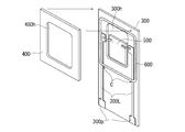
- a mixed potential type sensor element 500 that detects the concentration of a specific gas is suspended in the opening 300 h of the wiring board 300 by wire bonding or the like, and the measurement gas flows through the wiring board 300.
- a gas sensor having a structure in which a frame body 400 for forming an internal space 400h, a lid portion (not shown), and the like are stacked is known (Patent Document 1).
- the sensor element 500 includes a solid electrolyte body and a pair of electrodes, and each electrode is connected to a lead portion 300 ⁇ / b> L provided on the wiring substrate 300.
- the lead portion 300L extends to one end of the wiring substrate 300 and is integrally connected to the electrode pad 300p.
- a detection signal (electromotive force) generated between the pair of electrodes of the sensor element 500 is output to the outside through the lead portion 300L and the electrode pad 300p.
- the wiring substrate 300, the frame body 400, and the like are generally formed of an insulating ceramic such as alumina, and each member 300, 400 is formed in a frame shape so as to surround the sensor element 50, and is made of glass or inorganic material. Adhesive lamination using an adhesive 600 is also performed. In this case, the adhesive 600 is applied in a frame shape so as to surround the internal space (opening) 400h of the frame body 400 and straddle the lead portion 300L, and the adhesive 600 and the lead portion 300L are in contact at the contact C. Become.
- the resistance of the adhesive 600 is high (for example, several tens of G ⁇ ), in the case of the mixed potential type sensor element 500, the resistance between the pair of electrodes is high (for example, several G ⁇ ) and is connected to each electrode.
- the resistance between the pair of lead portions 300L is also high. Therefore, when a leak current flows between the contacts C through the adhesive 600, the detection signal (electromotive force) is reduced from the sensor element 500 obtained through the lead portion 300L, and the gas detection accuracy may be reduced.
- a gas sensor is provided with a pair of electrodes on a solid electrolyte body, and detects a gas of a specific component in a gas to be measured, and the mixed potential sensor unit.
- a pair of first lead portions that are respectively electrically connected to the pair of electrodes of the mixed potential type sensor portion are provided on one surface
- a first adhesive layer formed in a frame shape so as to surround the periphery of the mixed potential type sensor unit, so that a part of the one surface of the ceramic wiring board is exposed in a region inside the first adhesive layer.
- a gas sensor comprising: a first adhesive layer provided on the one surface of the ceramic wiring substrate; and a laminated member laminated on the one surface of the ceramic wiring substrate via the first adhesive layer. And At least one of the pair of first lead portions is disposed in a region inside the first adhesive layer and electrically connected to a through conductor penetrating the ceramic wiring substrate in the region, and the ceramic wiring A second lead portion that is electrically connected to the through conductor and extends to a portion outside the first adhesive layer is provided on the opposite surface of the substrate.
- the first lead portion provided on one surface of the ceramic wiring substrate is disposed in a region inside the first adhesive layer, and the second lead portion provided on the surface on the opposite side of the ceramic wiring substrate. Is connected to the first lead portion via a through conductor provided in the inner region.
- the ceramic wiring board is formed on the opening, the one surface, and located on the outer side of the opening, and connected to the pair of first leads, respectively.
- the mixed potential type sensor unit is suspended and fixed in the opening, and is welded to the element peripheral pad via a current-carrying member, and the first adhesive layer is disposed outside the element peripheral pad. It may be. According to this gas sensor, it is possible to suppress the sealing portion from sandwiching the current-carrying member connected to the element peripheral pad, stably weld the current-carrying member and the element peripheral pad, and increase the bonding strength between them.
- the gas sensor of the present invention is formed in a frame shape so as to surround the periphery of the mixed potential type sensor unit, and is a second adhesive layer provided on the opposite surface of the ceramic wiring board, and its outer edge is the A second adhesive layer located on the inner side of the inner edge of the first adhesive layer, and the through conductor is formed along the inner edge of the first adhesive layer and the inner edge when viewed in the thickness direction of the ceramic wiring board. It is good to be provided between the outer edges of the second adhesive layer. Even when the frame-like second adhesive layer is disposed on the opposite surface of the ceramic wiring substrate, the relationship between the first adhesive layer and the second adhesive layer and the arrangement position of the through conductors are set as described above. Thus, no leakage current flows between the lead portions through the adhesive layer, and a decrease in gas detection accuracy can be suppressed.
- the present invention it is possible to suppress a decrease in gas detection accuracy in a configuration in which a laminated member is laminated via an adhesive layer on a ceramic wiring substrate that fixes a mixed potential type sensor unit.
- FIG. 2 is a cross-sectional view taken along line AA in FIG. It is a perspective view which shows the aspect which laminates
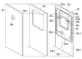
- FIG. 1 is an exploded perspective view of a gas sensor 100 including a mixed potential sensor unit 222 according to an embodiment of the present invention.
- FIG. 2 shows a ceramic wiring board 30 on the mixed potential sensor unit 222 side through a first adhesive layer 66.
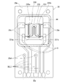
- FIG. 3 is a plan view showing the ceramic wiring board 30 on the opposite side of the mixed potential sensor unit 222, and
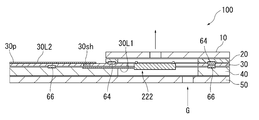
- FIG. 4 is a cross-sectional view taken along the line AA in FIG. In FIG. 1, the upper side is “upper” and the lower side is “lower”.
- the gas sensor 100 includes a sensor unit 200 including a mixed potential type sensor unit 222, a ceramic wiring board 30 that suspends and fixes the sensor unit 200, and a rectangular frame-shaped first arranged above the ceramic wiring board 30.
- the sensor unit 200 has a substantially rectangular plate shape.
- the heater unit 220 and the temperature sensor 221 are arranged on the upper surface, and a plurality of mixed potential type sensor units 222 are arranged in series on the lower surface opposite to the upper surface.
- concentration of a specific gas in the gas to be measured is measured.
- On the upper surface of the sensor unit 200 as shown in FIG. 3, current-carrying pads 220a and 220b are formed on both ends of the upper side of the sensor unit 200.
- the temperature sensor 221 extends meandering along the heater unit 220 on the upper surface of the sensor unit 200, and energization pads 221 a and 221 b that form both ends of the temperature sensor 221 are formed on both ends of the lower side of the sensor unit 200. ing.
- the ceramic wiring board 30 has a rectangular shape and has a rectangular opening 30h on one end side in the longitudinal direction.
- a plurality of second lead parts 30L2, which will be described later, are arranged on the surface of the ceramic wiring board 30 (upper surface in FIG. 1).
- six second lead portions 30L2 are provided, and one end of the four second lead portions 30L2 is connected to a plurality of element peripheral pads 30s surrounding the opening 30h, and six second lead portions 30L2 are connected.
- the lead portions 30L2 one end of the remaining two second lead portions 30L (the leftmost side in FIG. 1 and the fourth from the left side) is not connected to the element peripheral pad 30s and is closer to the center of the ceramic wiring board 30.
- each is connected to two through conductors 30sh described later.
- the other end of each second lead portion 30L2 is connected to the conductive pad portion 30p on the opposite side of the opening 30h in the longitudinal direction of the ceramic wiring substrate 30.
- the sensor unit 200 is accommodated in the opening 30h, and a total of four energization members 30w are arranged across the left and right sides of the sensor unit 200, and the energization pads 220a, 220b, 221a, 221b of the sensor unit 200 are combined. And four element peripheral pads 30s of the ceramic wiring board 30 are welded and joined. Thereby, the sensor unit 200 is suspended and fixed in the opening 30 h of the ceramic wiring substrate 30.
- two element peripheral pads 30 s are also provided around the opening 30 h on the lower surface 30 f side of the ceramic wiring substrate 30, and the element peripheral pads 30 s are connected to a first lead portion 30 ⁇ / b> L ⁇ b> 1 described in detail later. It is connected.
- the mixed potential sensor unit 222 has an electrode for taking out a detection signal (electromotive force) generated between a pair of electrodes (a series circuit when a plurality of mixed potential sensor units 222 are connected in series). Pads 222a and 222b are formed.
- the current supply member 30w is welded to each electrode pad 222a, 222b and each element peripheral pad 30s so that they are electrically connected.
- the other ends of the two first lead portions 30L1 are connected to the two second lead portions 30L2 on the opposite surface (upper surface) 30e side through the through conductors 30sh, respectively, and conductive pads It is connected to the part 30p.
- the electrical signals output from the mixed potential type sensor unit 222 and the temperature sensor 221 are output to the outside through the conductive pad unit 30p, and the heater unit is supplied with the electric power supplied from the outside through the conductive pad unit 30p. 220 is energized and heated.
- the element peripheral pad 30s formed on the lower surface 30f side of the ceramic wiring board 30 corresponds to an “element peripheral pad” in the claims.
- the first spacer 20 has a square shape and a rectangular opening 20h.
- the opening 20h overlaps the opening 30h and is larger than the opening 30h.
- the lid portion 10 has a square shape with the same dimensions as the first spacer 20, and a gas discharge hole 10h is provided in a portion of the lid portion 10 that faces the opening 20h.
- the second spacer 40 has a rectangular shape with the same dimensions as the ceramic wiring board 30 and has a rectangular opening 40h on the opening 30h side in the longitudinal direction.
- the opening 40h overlaps the opening 30h and is larger than the opening 30h.
- the base 50 has a rectangular shape with the same dimensions as the ceramic wiring board 30, and a gas introduction hole 50 h is provided in a portion of the base 50 that faces the opening 40 h.
- the ceramic wiring substrate 30, the first spacer 20, the lid 10, the second spacer 40, and the base 50 can be formed from an insulating ceramic such as alumina or mullite.
- seal portions 64 and 62 are disposed between the ceramic wiring substrate 30 and the first spacer 20 and between the first spacer 20 and the lid portion 10 and outside the opening 20h, respectively.
- rectangular seal portions 66 and 68 are disposed between the ceramic wiring substrate 30 and the second spacer 40 and between the second spacer 40 and the base portion 50 and outside the opening 40h, respectively.
- the seal portions 66 and 68 extend from the seal portions 64 and 62 in the longitudinal direction of the ceramic wiring substrate 30 toward the conductive pad portion 30p.
- each of the seal portions 62, 64, 66, 68 is formed in a frame shape (specifically, a square frame shape) so as to surround the hybrid potential type sensor portion 222.
- the seal portions 64 and 66 are formed to have a size that exposes a part of the surface (upper surface or lower surface) of the ceramic wiring board in a region inside the seal portion 64, and the outer edge of the seal portion 64 is the seal portion.
- the size of each seal portion 64, 66 and the installation position on the ceramic wiring board 30 are adjusted so as to be located inside the inner edge of 66.
- Each seal part 62, 64, 66, 68 is made of glass or an inorganic adhesive.
- the seal portion 66 corresponds to a “first adhesive layer” in the claims, and the seal portion 64 corresponds to a “second adhesive layer” in the claims.
- the second spacer 40 corresponds to a “laminated member” in the claims.
- the lid portion 10, the first spacer 20, the ceramic wiring substrate 30, the second spacer 40, and the base portion 50 are hermetically bonded and stacked via the seal portions 62 to 68.
- Positioning holes 30a are provided at both ends on the opening 30h side in the longitudinal direction of the ceramic wiring board 30, and similarly, positioning holes 30b are provided at both ends on the conductive pad portion 30p side.
- Positioning holes 20a and 10a are provided at positions overlapping the positioning hole 30a in the first spacer 20 and the lid portion 10, respectively.
- positioning holes 40a and 40b are provided in the second spacer 40 at positions overlapping the positioning holes 30a and 30b, respectively.
- Positioning holes 50a and 50b are provided in the base 50 at positions overlapping the positioning holes 30a and 30b, respectively.
- the gas sensor 100 can be assembled by inserting a jig (guide pin) through the substrate, positioning each member, and bonding the members. Thereby, the gas G to be measured introduced from the gas introduction hole 50h comes into contact with the mixed potential type sensor unit 222 of the sensor unit 200 through the internal space formed by the opening 40h, and the concentration of the specific gas (for example, NOx) is reduced. After being measured, the gas is discharged from the gas discharge hole 10h to the outside through the internal space formed by the opening 20h.
- a jig guide pin
- the mixed potential type sensor unit 222 of the sensor unit 200 is suspended and fixed toward one surface 30 f (corresponding to the lower surface of FIG. 1) of the ceramic wiring substrate 30.
- Two element peripheral pads 30s are provided on the lower surface 30f of the ceramic wiring substrate 30, and one end of the first lead portion 30L1 is connected to each element peripheral pad 30s, and the other end of each first lead portion 30L1 is connected to the ceramic wiring.
- Each of the through conductors 30 sh is electrically connected to a position slightly below the opening 30 h of the substrate 30.
- Each through conductor 30sh penetrates the ceramic wiring board 30 and is exposed to the opposite surface 30e (upper surface in FIG. 1) of the ceramic wiring board 30 as shown in FIG.
- the through conductor 30sh is formed by forming a through hole penetrating in the thickness direction of the ceramic wiring substrate 30, and printing and baking a conductive paste along the inner peripheral surface of the through hole. ing.
- Each through conductor 30sh is connected to two second lead portions 30L2 (the leftmost side and the fourth from the left side) on the opposite surface 30e.
- Each of the second lead portions 30L2 has one end connected to the through conductor 30sh and the other end connected to the conductive pad portion 30p.
- the lower surface 30f of the ceramic wiring substrate 30 and the second spacer 40 are hermetically bonded and stacked by a seal portion 66 extending in a square frame shape outside the opening 40h.
- Each first lead portion 30L1 is disposed only in a region inside the seal portion 66, and is electrically connected to the through conductor 30sh in this region.
- each second lead portion 30L2 connected to the through conductor 30sh extends to a portion outside the seal portion 66 on the opposite surface 30e of the ceramic wiring substrate 30, and is electrically connected to the conductive pad portion 30p. . Further, as shown in FIG.
- the through conductor 30 sh is provided between the inner edge of the seal portion 66 and the outer edge of the seal portion 64 when viewed along the thickness direction of the ceramic wiring substrate 30.
- the first lead portion 30L1 and the second lead portion 30L2 are not in contact with the seal portion 66.
- each first lead portion 30L1 provided on one surface (lower surface 30f) of the ceramic wiring substrate 30 is disposed in a region inside the seal portion 66 that is an adhesive layer, and the opposite surface of the ceramic wiring substrate 30.
- the resistance (insulation resistance) of the seal portion 66 may be reduced due to the influence of temperature or the like. Even if it exists, it can suppress that gas detection accuracy falls.
- the total resistance value of the electrodes is further increased, so that the present invention is more effective.
- the opposite surface 30e of the ceramic wiring board 30 and the first spacer 20 are air-tightly stacked by a square frame-shaped seal portion 64 outside the opening 20h.
- the electrical resistance (about several tens of ohms) of the second lead part 30L2 connected to the heater part 220 and the temperature sensor 221 is extremely lower than the electrical resistance of the seal part 64. Therefore, even if the second lead portion 30L2 contacts the seal portion 64 at the contact point D, the energization current of the heater portion 220 and the detection current of the temperature sensor 221 do not substantially leak through the seal portion 66.
- the seal portion 66 may be disposed outside the element peripheral pad 30s. If it does in this way, it will suppress that the seal
- the present invention is not limited to the above-described embodiment, but extends to various modifications and equivalents included in the spirit and scope of the present invention.
- the type of the mixed potential type sensor unit, the method for fixing the mixed potential type sensor unit to the ceramic wiring substrate, and the like are not limited to the above embodiment.
- at least one of the pair of first lead portions may be disposed in a region inside the adhesive layer. However, if both the pair of first lead portions are disposed in a region inside the adhesive layer, the gas A decrease in detection accuracy can be further suppressed.
- the conductive paste is printed and fired along the inner peripheral surface of the through hole formed in the ceramic wiring substrate 30 as the through conductor 30sh. However, the through hole formed in the ceramic wiring substrate 30 is formed. Alternatively, the conductive paste may be filled and fired.
- Ceramic wiring substrate 30e Opposite surface of ceramic wiring substrate 30f One surface of ceramic wiring substrate 30L1 First lead portion 30L2 Second lead portion 30sh Through conductor 30h Opening portion 30s Element peripheral pad 30w Current-carrying member 40 Laminating member 64 Seal portion 2 adhesive layers) 66 Sealing part (first adhesive layer) 100 Gas sensor 222 Hybrid potential type sensor unit
Landscapes
- Chemical & Material Sciences (AREA)
- Life Sciences & Earth Sciences (AREA)
- Health & Medical Sciences (AREA)
- Physics & Mathematics (AREA)
- Chemical Kinetics & Catalysis (AREA)
- Electrochemistry (AREA)
- Molecular Biology (AREA)
- Analytical Chemistry (AREA)
- Biochemistry (AREA)
- General Health & Medical Sciences (AREA)
- General Physics & Mathematics (AREA)
- Immunology (AREA)
- Pathology (AREA)
- Measuring Oxygen Concentration In Cells (AREA)
Abstract
混成電位型センサ部を固定するセラミック配線基板に接着層を介して積層部材を積層する構成において、ガス検出精度の低下を抑制したガスセンサを提供する。 混成電位型センサ部222と、混成電位型センサ部を固定し、混成電位型センサ部の一対の電極に接続される一対の第1リード部30L1が一方の面30fに設けられたセラミック配線基板30と、混成電位型センサ部の周囲を取り囲み、一方の面に設けられる枠状の第1接着層66と、一方の面に第1接着層を介して積層される積層部材40と、を備えたガスセンサ100であって、第1リード部の少なくとも一方は、第1接着層よりも内側の領域に配置されると共に当該領域にてセラミック配線基板を貫通する貫通導体30shに電気的に接続され、セラミック配線基板の反対面30eには、貫通導体に接続されて第1接着層よりも外側の部位に延びる第2リード部30L2が設けられてなる。
Description
本発明は、特定ガスの濃度を検知するガスセンサに関する。
図5に示すように、特定ガスの濃度を検知する混成電位型のセンサ素子500を配線基板300の開口部300h内にワイヤボンディング等で宙吊り固定し、この配線基板300に被測定ガスが流通する内部空間400hを形成するための枠体400や、図示しない蓋部等を積層した構造のガスセンサが知られている(特許文献1)。
センサ素子500は固体電解質体と一対の電極とを有し、各電極は、配線基板300上に設けられたリード部300Lに接続されている。リード部300Lは配線基板300の一端に延びて電極パッド300pに一体に接続されている。そして、センサ素子500の一対の電極間に生じる検知信号(起電力)は、リード部300L及び電極パッド300pを介して外部に出力される。
センサ素子500は固体電解質体と一対の電極とを有し、各電極は、配線基板300上に設けられたリード部300Lに接続されている。リード部300Lは配線基板300の一端に延びて電極パッド300pに一体に接続されている。そして、センサ素子500の一対の電極間に生じる検知信号(起電力)は、リード部300L及び電極パッド300pを介して外部に出力される。
配線基板300、枠体400等は一般にアルミナ等の絶縁性のセラミックから形成されており、各部材300、400を、センサ素子50の周囲を取り囲むように枠状に形成すると共に、ガラスや無機系の接着剤600を用いて接着して気密に積層することも行われている。この場合、枠体400の内部空間(開口部)400hを囲み、リード部300Lを跨ぐように枠状に接着剤600が塗布され、接着剤600とリード部300Lとが接点Cにて接することになる。
ガスセンサの温度が高くなり、接着剤600の抵抗(絶縁抵抗)が低下することがあると、接着剤600とリード部300Lとの接点C間にて接着剤600を通ってリーク電流が流れることがある。ここで、接着剤600の抵抗は高い(例えば、数十GΩ)が、混成電位型のセンサ素子500の場合、一対の電極間の抵抗が高く(例えば、数GΩ)、各電極と接続された一対のリード部300L間の抵抗も高くなっている。そのため、接着剤600を通じて接点C間にリーク電流が流れると、リード部300Lを通じて得られるセンサ素子500から検知信号(起電力)が低下することになり、ガス検出精度が低下するおそれがある。
そこで、本発明は、混成電位型センサ部からの検知信号をセラミック配線基板のリード部を介して外部に取り出すにあたり、セラミック配線基板に積層される積層部材を接着するための接着層が存在してもガス検出精度の低下が抑制されたガスセンサを提供することを目的とする。
そこで、本発明は、混成電位型センサ部からの検知信号をセラミック配線基板のリード部を介して外部に取り出すにあたり、セラミック配線基板に積層される積層部材を接着するための接着層が存在してもガス検出精度の低下が抑制されたガスセンサを提供することを目的とする。
上記課題を解決するため、本発明のガスセンサは、固体電解質体に一対の電極を設けてなり、被測定ガス中の特定成分のガスを検出する混成電位型センサ部と、前記混成電位型センサ部を直接又は他部材を介して間接的に固定し、前記混成電位型センサ部の前記一対の電極にそれぞれ電気的に接続される一対の第1リード部が一方の面に設けられたセラミック配線基板と、前記混成電位型センサ部の周囲を取り囲むように枠状に形成される第1接着層であって、自身の内側の領域に前記セラミック配線基板の前記一方の面の一部を露出させるように当該セラミック配線基板の前記一方の面に設けられる第1接着層と、前記セラミック配線基板の前記一方の面に前記第1接着層を介して積層される積層部材と、を備えたガスセンサであって、前記一対の第1リード部の少なくとも一方は、前記第1接着層よりも内側の領域に配置されると共に当該領域にて前記セラミック配線基板を貫通する貫通導体に電気的に接続され、前記セラミック配線基板の反対面には前記貫通導体に電気的に接続されて前記第1接着層よりも外側の部位に延びる第2リード部が設けられてなることを特徴とする。
このガスセンサによれば、セラミック配線基板の一方の面に設けられる第1リード部を第1接着層よりも内側の領域に配置すると共に、セラミック配線基板の反対側の面に設けられる第2リード部を上記の内側の領域に設けられた貫通導体を経由して第1リード部に接続させている。これにより、混成電位型センサ部の検知信号をセラミック配線基板のリード部を通じて外部に取り出すにあたり、リード部(第1リード部、第2リード部)が第1接着層に接することがない。したがって、第1接着層の抵抗(絶縁抵抗)が低下することがあったとしても、ガス検出精度が低下するのを抑制することができる。
特に、混成電位型センサ部が複数個直列に接続されている場合、電極を合計した抵抗値がさらに高くなるので、本発明がより有効となる。
特に、混成電位型センサ部が複数個直列に接続されている場合、電極を合計した抵抗値がさらに高くなるので、本発明がより有効となる。
本発明のガスセンサにおいて、前記セラミック配線基板は、開口部と、前記一方の面に形成され且つ該開口部の外側に位置すると共に、前記一対の第1リード部にそれぞれ接続される一対の素子周辺パッドとを備え、前記混成電位型センサ部は前記開口部に宙吊り固定されると共に、前記素子周辺パッドに通電部材を介して溶接され、前記第1接着層は前記素子周辺パッドの外側に配置されていてよい。
このガスセンサによれば、シール部が素子周辺パッドに接続された通電部材を挟み込むことを抑制し、通電部材と素子周辺パッドとの溶接を安定して行え、両者の接合強度を高められる。
このガスセンサによれば、シール部が素子周辺パッドに接続された通電部材を挟み込むことを抑制し、通電部材と素子周辺パッドとの溶接を安定して行え、両者の接合強度を高められる。
本発明のガスセンサにおいて、前記混成電位型センサ部の周囲を取り囲むように枠状に形成されると共に、前記セラミック配線基板の前記反対面に設けられる第2接着層であって、自身の外縁が前記第1接着層の内縁よりも内側に位置してなる第2接着層を備え、前記貫通導体は、前記セラミック配線基板の厚み方向に沿って見たときに、前記第1接着層の内縁と前記第2接着層の外縁との間に設けられているとよい。
セラミック配線基板の反対面に枠状の第2接着層が配置される場合にも、第1接着層と第2接着層との関係、及び、貫通導体の配置位置を上記のように設定することで、接着層を通じてリード部間にリーク電流が流れることがなく、ガス検出精度の低下を抑制することができる。
セラミック配線基板の反対面に枠状の第2接着層が配置される場合にも、第1接着層と第2接着層との関係、及び、貫通導体の配置位置を上記のように設定することで、接着層を通じてリード部間にリーク電流が流れることがなく、ガス検出精度の低下を抑制することができる。
この発明によれば、混成電位型センサ部を固定するセラミック配線基板に対して、接着層を介して積層部材を積層する構成において、ガス検出精度の低下を抑制することができる。
以下に、本発明を、図面を参照しながら詳細に説明する。図1は、本発明の実施形態における混成電位型センサ部222を含むガスセンサ100の分解斜視図、図2は混成電位型センサ部222側のセラミック配線基板30を、第1接着層66を介して積層する態様を示す斜視図、図3は混成電位型センサ部222と反対面のセラミック配線基板30を示す平面図、図4は図1のA-A線に沿う断面図である。なお、図1の上側を「上方」とし、下側を「下方」とする。
図1において、ガスセンサ100は、混成電位型センサ部222を含むセンサユニット200と、センサユニット200を宙吊り固定するセラミック配線基板30と、セラミック配線基板30の上方に配置される矩形枠状の第1スペーサ20と、第1スペーサ20の上方に配置される蓋部10と、セラミック配線基板30の下方に配置される矩形枠状の第2スペーサ40と、第2スペーサ40の下方に配置される基部50と、を備えている。
センサユニット200は略矩形板状をなし、上面にヒータ部220及び温度センサ221が配置され、上面とは反対側に位置する下面には混成電位型センサ部222が複数個直列に接続して配置され、被測定ガス中の特定ガスの濃度を測定するようになっている。
なお、センサユニット200の上面には、図3に示すように、センサユニット200の上辺の両端側に、蛇行して延びるヒータ部220の両端をなす通電用パッド220a、220bが形成されている。又、温度センサ221は、センサユニット200の上面においてヒータ部220に沿って蛇行して伸び、センサユニット200の下辺の両端側に、温度センサ221の両端をなす通電用パッド221a、221bが形成されている。
なお、センサユニット200の上面には、図3に示すように、センサユニット200の上辺の両端側に、蛇行して延びるヒータ部220の両端をなす通電用パッド220a、220bが形成されている。又、温度センサ221は、センサユニット200の上面においてヒータ部220に沿って蛇行して伸び、センサユニット200の下辺の両端側に、温度センサ221の両端をなす通電用パッド221a、221bが形成されている。
セラミック配線基板30は、長方形状をなし、長手方向の一端側に矩形の開口部30hを有し、セラミック配線基板30の表面(図1の上面)には後述する第2リード部30L2が複数配置されている。本実施形態では、6本の第2リード部30L2が設けられ、そのうち4本の第2リード部30L2の一端は、開口部30hを囲む複数の素子周辺パッド30sに接続されて6本の第2リード部30L2のうち、残り2本の第2リード部30L(図1の最左側と、左側から4本目)の一端は、素子周辺パッド30sに繋がらず、セラミック配線基板30の中央部寄りで、後述する2つの貫通導体30shにそれぞれ繋がっている。また、各第2リード部30L2の他端は、セラミック配線基板30の長手方向に開口部30hの反対側にて導電パッド部30pにそれぞれ接続されている。
そして、開口部30h内にセンサユニット200が収容され、センサユニット200の左右の辺をそれぞれ跨ぐようにして、合計4本の通電部材30wがセンサユニット200の通電用パッド220a、220b、221a、221bと、セラミック配線基板30の4つの素子周辺パッド30sとに溶接して接合されている。これにより、センサユニット200がセラミック配線基板30の開口部30h内に宙吊り固定されている。
そして、開口部30h内にセンサユニット200が収容され、センサユニット200の左右の辺をそれぞれ跨ぐようにして、合計4本の通電部材30wがセンサユニット200の通電用パッド220a、220b、221a、221bと、セラミック配線基板30の4つの素子周辺パッド30sとに溶接して接合されている。これにより、センサユニット200がセラミック配線基板30の開口部30h内に宙吊り固定されている。
図2に示すように、セラミック配線基板30の下面30f側にも、開口部30hの周囲に2つの素子周辺パッド30sが設けられ、素子周辺パッド30sは、詳しくは後述する第1リード部30L1に接続されている。また、混成電位型センサ部222には、一対の電極(混成電位型センサ部222が複数個直列に接続されている場合、その直列回路)間に生じる検知信号(起電力)を取り出すための電極パッド222a、222bが形成されている。
そして、各電極パッド222a、222bと、各素子周辺パッド30sとに、それぞれ通電部材30wが溶接されることで両者が電気的に接続されている。
さらに、詳しくは後述するが、2本の第1リード部30L1の他端が、貫通導体30shを介して反対面(上面)30e側の2本の第2リード部30L2とそれぞれ接続され、導電パッド部30pに接続されるようになっている。
そして、各電極パッド222a、222bと、各素子周辺パッド30sとに、それぞれ通電部材30wが溶接されることで両者が電気的に接続されている。
さらに、詳しくは後述するが、2本の第1リード部30L1の他端が、貫通導体30shを介して反対面(上面)30e側の2本の第2リード部30L2とそれぞれ接続され、導電パッド部30pに接続されるようになっている。
このようにして、混成電位型センサ部222及び温度センサ221から出力された電気信号は導電パッド部30pを介して外部に出力され、導電パッド部30pを介して外部から供給された電力によりヒータ部220が通電加熱する。
なお、セラミック配線基板30の下面30f側に形成される素子周辺パッド30sが、特許請求の範囲の「素子周辺パッド」に相当する。
なお、セラミック配線基板30の下面30f側に形成される素子周辺パッド30sが、特許請求の範囲の「素子周辺パッド」に相当する。
第1スペーサ20は正方形状をなすと共に矩形の開口部20hを有し、開口部20hは開口部30hに重なると共に開口部30hよりも大きい。
蓋部10は、第1スペーサ20と同一寸法の正方形状をなし、蓋部10のうち開口部20hに対向する部位にガス排出孔10hが設けられている。
第2スペーサ40はセラミック配線基板30と同一寸法の長方形状をなし、長手方向に開口部30h側に矩形の開口部40hを有している。開口部40hは開口部30hに重なると共に開口部30hよりも大きい。
又、基部50はセラミック配線基板30と同一寸法の長方形状をなし、基部50のうち開口部40hに対向する部位にはガス導入孔50hが設けられている。
これらのセラミック配線基板30、第1スペーサ20、蓋部10、第2スペーサ40、基部50は、例えばアルミナやムライト等の絶縁性のセラミックから形成することができる。
又、セラミック配線基板30と第1スペーサ20の間、及び第1スペーサ20と蓋部10の間であって開口部20hよりも外側の位置に、それぞれ正方形状のシール部64、62が配置されている。同様に、セラミック配線基板30と第2スペーサ40の間、及び第2スペーサ40と基部50の間であって開口部40hよりも外側の位置に、それぞれ長方形状のシール部66、68が配置されている。
なお、シール部66、68は、セラミック配線基板30の長手方向に導電パッド部30p側に向かって、シール部64、62よりも延びている。
ここで、各シール部62、64、66、68は、混成電位型センサ部222の周囲を取り囲むように枠状(具体的には四角枠状)に形成されている。そして、シール部64、66は、自身の内側の領域にセラミック配線基板の表面(上面又は下面)の一部を露出させる大きさに形成されており、また、シール部64の外縁は、シール部66の内縁よりも内側に位置するように、各シール部64、66の大きさやセラミック配線基板30への設置位置が調整されている。
各シール部62、64、66、68は、ガラスや無機系の接着剤からなる。なお、シール部66が特許請求の範囲の「第1接着層」に相当し、シール部64が特許請求の範囲の「第2接着層」に相当する。又、第2スペーサ40が特許請求の範囲の「積層部材」に相当する。
そして、本実施形態では、蓋部10、第1スペーサ20、セラミック配線基板30、第2スペーサ40、基部50の間が、シール部62~68を介して気密に接着されて積層されている。
セラミック配線基板30の長手方向に開口部30h側の両端には位置決め孔30aがそれぞれ設けられ、同様に導電パッド部30p側の両端には位置決め孔30bがそれぞれ設けられている。
そして、第1スペーサ20及び蓋部10のうち、位置決め孔30aに重なる位置にそれぞれ位置決め孔20a、10aが設けられている。
同様に、第2スペーサ40のうち、位置決め孔30a、30bに重なる位置にそれぞれ位置決め孔40a、40bが設けられている。又、基部50のうち、位置決め孔30a、30bに重なる位置にそれぞれ位置決め孔50a、50bが設けられている。
そして、第1スペーサ20及び蓋部10のうち、位置決め孔30aに重なる位置にそれぞれ位置決め孔20a、10aが設けられている。
同様に、第2スペーサ40のうち、位置決め孔30a、30bに重なる位置にそれぞれ位置決め孔40a、40bが設けられている。又、基部50のうち、位置決め孔30a、30bに重なる位置にそれぞれ位置決め孔50a、50bが設けられている。
そして、蓋部10、第1スペーサ20、セラミック配線基板30、第2スペーサ40及び基部50(これらを「各部材」ともいう)をこの順で積層し、各位置決め孔10a~50a、40b、50bに治具(ガイドピン)を挿通して各部材を位置決めし、各部材を接着することで、ガスセンサ100を組み付けることができる。
これにより、ガス導入孔50hから導入された被測定ガスGは、開口部40hからなる内部空間を経てセンサユニット200の混成電位型センサ部222に接触して特定ガス(例えば、NOx)の濃度が測定された後、開口部20hからなる内部空間を経てガス排出孔10hから外部に排出される。
これにより、ガス導入孔50hから導入された被測定ガスGは、開口部40hからなる内部空間を経てセンサユニット200の混成電位型センサ部222に接触して特定ガス(例えば、NOx)の濃度が測定された後、開口部20hからなる内部空間を経てガス排出孔10hから外部に排出される。
次に、図2~図4を参照し、混成電位型センサ222側のガスセンサを、接着層66を介して積層する態様について説明する。
図2に示すように、センサユニット200の混成電位型センサ部222は、セラミック配線基板30の一方の面30f(図1の下面に相当)に向いて宙吊り固定されている。
セラミック配線基板30の下面30fには2つの素子周辺パッド30sが設けられ、各素子周辺パッド30sにそれぞれ第1リード部30L1の一端が接続され、各第1リード部30L1の他端は、セラミック配線基板30の開口部30hよりやや下方の位置でそれぞれ貫通導体30shに電気的に接続されている。各貫通導体30shはセラミック配線基板30を貫通し、図3に示すようにセラミック配線基板30の反対面30e(図1の上面)に表出している。なお、本実施形態では、貫通導体30shは、セラミック配線基板30の厚み方向に貫通するスルーホールを形成し、そのスルーホールの内周面に沿うように導電ペーストを印刷、焼成することで形成されている。そして、反対面30eにて各貫通導体30shが2つ(最左側と、左側から4本目)の第2リード部30L2にそれぞれ接続されている。この第2リード部30L2は、いずれも自身の一端が貫通導体30shに接続され、他端が導電パッド部30pに接続されている。
セラミック配線基板30の下面30fと、第2スペーサ40とは、開口部40hより外側で四角枠状に切れ目なく延びたシール部66により気密に接着されて積層されている。又、各第1リード部30L1は、シール部66よりも内側の領域にのみ配置されると共に、この領域にて貫通導体30shに電気的に接続されている。
一方、貫通導体30shに接続された各第2リード部30L2は、セラミック配線基板30の反対面30eにてシール部66よりも外側の部位に延び、導電パッド部30pに電気的に接続されている。
また、貫通導体30shは、図4に示すように、セラミック配線基板30の厚み方向に沿って見たときに、シール部66の内縁とシール部64の外縁との間に設けられており、第1リード部30L1および第2リード部30L2は、シール部66に対して非接触の状態となっている。
一方、貫通導体30shに接続された各第2リード部30L2は、セラミック配線基板30の反対面30eにてシール部66よりも外側の部位に延び、導電パッド部30pに電気的に接続されている。
また、貫通導体30shは、図4に示すように、セラミック配線基板30の厚み方向に沿って見たときに、シール部66の内縁とシール部64の外縁との間に設けられており、第1リード部30L1および第2リード部30L2は、シール部66に対して非接触の状態となっている。
このように、セラミック配線基板30の一方の面(下面30f)に設けられる各第1リード部30L1を接着層であるシール部66よりも内側の領域に配置すると共に、セラミック配線基板30の反対面30e(上面)に設けられる第2リード部30L2を貫通導体30shを経由して第1リード部30L1と接続させることで、シール部66の抵抗(絶縁抵抗)が温度等の影響により低下することがあったとしても、ガス検出精度が低下するのを抑制ことができる。
特に、混成電位型センサ部222が複数個直列に接続されている場合、電極を合計した抵抗値がさらに高くなるので、本発明がより有効となる。
特に、混成電位型センサ部222が複数個直列に接続されている場合、電極を合計した抵抗値がさらに高くなるので、本発明がより有効となる。
なお、図3に示すように、セラミック配線基板30の反対面30eと、第1スペーサ20とは、開口部20hより外側で四角枠状のシール部64により気密に積層されている。
しかしながら、ヒータ部220及び温度センサ221に接続される第2リード部30L2の電気抵抗(数十Ω程度)は、シール部64の電気抵抗よりも極めて低い。そのため、第2リード部30L2が接点Dでシール部64と接しても、ヒータ部220の通電電流や、温度センサ221の検知電流がシール部66を通ってリークすることは実質的に無い。
しかしながら、ヒータ部220及び温度センサ221に接続される第2リード部30L2の電気抵抗(数十Ω程度)は、シール部64の電気抵抗よりも極めて低い。そのため、第2リード部30L2が接点Dでシール部64と接しても、ヒータ部220の通電電流や、温度センサ221の検知電流がシール部66を通ってリークすることは実質的に無い。
なお、図2に示すように、シール部66は素子周辺パッド30sの外側に配置されているとよい。このようにすると、シール部66が素子周辺パッド30sに接続された細長い通電部材30wを挟み込むことを抑制し、通電部材30wと素子周辺パッドとの溶接を安定して行え、両者の接合強度を高められる。
本発明は上記実施形態に限定されず、本発明の思想と範囲に含まれる様々な変形及び均等物に及ぶことはいうまでもない。
混成電位型センサ部の種類、セラミック配線基板への混成電位型センサ部の固定方法等は上記実施形態に限定されない。
又、一対の第1リード部のうち、少なくとも一方が接着層よりも内側の領域に配置されていればよいが、一対の第1リード部を共に接着層よりも内側の領域に配置すると、ガス検出精度の低下を一層抑制することができる。さらに、上記実施形態では、貫通導体30shとしてセラミック配線基板30に形成したスルーホールの内周面に沿うように導電ペーストを印刷、焼成することで形成したが、セラミック配線基板30に形成したスルーホールに導電ペーストを充填、焼成することで形成してもよい。
混成電位型センサ部の種類、セラミック配線基板への混成電位型センサ部の固定方法等は上記実施形態に限定されない。
又、一対の第1リード部のうち、少なくとも一方が接着層よりも内側の領域に配置されていればよいが、一対の第1リード部を共に接着層よりも内側の領域に配置すると、ガス検出精度の低下を一層抑制することができる。さらに、上記実施形態では、貫通導体30shとしてセラミック配線基板30に形成したスルーホールの内周面に沿うように導電ペーストを印刷、焼成することで形成したが、セラミック配線基板30に形成したスルーホールに導電ペーストを充填、焼成することで形成してもよい。
30 セラミック配線基板
30e セラミック配線基板の反対面
30f セラミック配線基板の一方の面
30L1 第1リード部
30L2 第2リード部
30sh 貫通導体
30h 開口部
30s 素子周辺パッド
30w 通電部材
40 積層部材
64 シール部(第2接着層)
66 シール部(第1接着層)
100 ガスセンサ
222 混成電位型センサ部
30e セラミック配線基板の反対面
30f セラミック配線基板の一方の面
30L1 第1リード部
30L2 第2リード部
30sh 貫通導体
30h 開口部
30s 素子周辺パッド
30w 通電部材
40 積層部材
64 シール部(第2接着層)
66 シール部(第1接着層)
100 ガスセンサ
222 混成電位型センサ部
Claims (3)
- 固体電解質体に一対の電極を設けてなり、被測定ガス中の特定成分のガスを検出する混成電位型センサ部と、
前記混成電位型センサ部を直接又は他部材を介して間接的に固定し、前記混成電位型センサ部の前記一対の電極にそれぞれ電気的に接続される一対の第1リード部が一方の面に設けられたセラミック配線基板と、
前記混成電位型センサ部の周囲を取り囲むように枠状に形成される第1接着層であって、自身の内側の領域に前記セラミック配線基板の前記一方の面の一部を露出させるように当該セラミック配線基板の前記一方の面に設けられる第1接着層と、
前記セラミック配線基板の前記一方の面に前記第1接着層を介して積層される積層部材と、
を備えたガスセンサであって、
前記一対の第1リード部の少なくとも一方は、前記第1接着層よりも内側の領域に配置されると共に当該領域にて前記セラミック配線基板を貫通する貫通導体に電気的に接続され、
前記セラミック配線基板の前記一方の面とは反対側に位置する反対面には、前記貫通導体に電気的に接続されて前記第1接着層よりも外側の部位に延びる第2リード部が設けられてなることを特徴とするガスセンサ。 - 前記セラミック配線基板は、開口部と、前記一方の面に形成され且つ該開口部の外側に位置すると共に、前記一対の第1リード部にそれぞれ接続される一対の素子周辺パッドとを備え、
前記混成電位型センサ部は前記開口部に宙吊り固定されると共に、前記素子周辺パッドに通電部材を介して電気的に接続され、
前記第1接着層は前記素子周辺パッドの外側に配置されていることを特徴とする請求項1に記載のガスセンサ。 - 前記混成電位型センサ部の周囲を取り囲むように枠状に形成されると共に、前記セラミック配線基板の前記反対面に設けられる第2接着層であって、自身の外縁が前記第1接着層の内縁よりも内側に位置してなる第2接着層を備え、
前記貫通導体は、前記セラミック配線基板の厚み方向に沿って見たときに、前記第1接着層の内縁と前記第2接着層の外縁との間に設けられていることを特徴とする請求項1または請求項2に記載のガスセンサ。
Applications Claiming Priority (2)
| Application Number | Priority Date | Filing Date | Title |
|---|---|---|---|
| JP2016-218732 | 2016-11-09 | ||
| JP2016218732A JP2018077119A (ja) | 2016-11-09 | 2016-11-09 | ガスセンサ |
Publications (1)
| Publication Number | Publication Date |
|---|---|
| WO2018088241A1 true WO2018088241A1 (ja) | 2018-05-17 |
Family
ID=62109544
Family Applications (1)
| Application Number | Title | Priority Date | Filing Date |
|---|---|---|---|
| PCT/JP2017/038855 Ceased WO2018088241A1 (ja) | 2016-11-09 | 2017-10-27 | ガスセンサ |
Country Status (2)
| Country | Link |
|---|---|
| JP (1) | JP2018077119A (ja) |
| WO (1) | WO2018088241A1 (ja) |
Cited By (2)
| Publication number | Priority date | Publication date | Assignee | Title |
|---|---|---|---|---|
| WO2019163775A1 (ja) * | 2018-02-21 | 2019-08-29 | 日本特殊陶業株式会社 | ガスセンサおよびガスセンサの製造方法 |
| WO2019187853A1 (ja) * | 2018-03-30 | 2019-10-03 | 日本特殊陶業株式会社 | センサ |
Families Citing this family (1)
| Publication number | Priority date | Publication date | Assignee | Title |
|---|---|---|---|---|
| JP7617864B2 (ja) * | 2022-02-09 | 2025-01-20 | 株式会社Soken | ガスセンサ素子及びガスセンサ |
Citations (6)
| Publication number | Priority date | Publication date | Assignee | Title |
|---|---|---|---|---|
| JPS4933889U (ja) * | 1972-06-26 | 1974-03-25 | ||
| JPS61284653A (ja) * | 1985-06-12 | 1986-12-15 | Toshiba Corp | ガスセンサ |
| JPH11125618A (ja) * | 1997-08-22 | 1999-05-11 | Nok Corp | バイオセンサ |
| JP2006064476A (ja) * | 2004-08-25 | 2006-03-09 | Ngk Spark Plug Co Ltd | ガスセンサ |
| JP2007298508A (ja) * | 2006-04-29 | 2007-11-15 | Paragon Ag | センサ |
| WO2015134895A1 (en) * | 2014-03-07 | 2015-09-11 | Spirometrix, Inc. | Respiratory monitor |
-
2016
- 2016-11-09 JP JP2016218732A patent/JP2018077119A/ja active Pending
-
2017
- 2017-10-27 WO PCT/JP2017/038855 patent/WO2018088241A1/ja not_active Ceased
Patent Citations (6)
| Publication number | Priority date | Publication date | Assignee | Title |
|---|---|---|---|---|
| JPS4933889U (ja) * | 1972-06-26 | 1974-03-25 | ||
| JPS61284653A (ja) * | 1985-06-12 | 1986-12-15 | Toshiba Corp | ガスセンサ |
| JPH11125618A (ja) * | 1997-08-22 | 1999-05-11 | Nok Corp | バイオセンサ |
| JP2006064476A (ja) * | 2004-08-25 | 2006-03-09 | Ngk Spark Plug Co Ltd | ガスセンサ |
| JP2007298508A (ja) * | 2006-04-29 | 2007-11-15 | Paragon Ag | センサ |
| WO2015134895A1 (en) * | 2014-03-07 | 2015-09-11 | Spirometrix, Inc. | Respiratory monitor |
Cited By (2)
| Publication number | Priority date | Publication date | Assignee | Title |
|---|---|---|---|---|
| WO2019163775A1 (ja) * | 2018-02-21 | 2019-08-29 | 日本特殊陶業株式会社 | ガスセンサおよびガスセンサの製造方法 |
| WO2019187853A1 (ja) * | 2018-03-30 | 2019-10-03 | 日本特殊陶業株式会社 | センサ |
Also Published As
| Publication number | Publication date |
|---|---|
| JP2018077119A (ja) | 2018-05-17 |
Similar Documents
| Publication | Publication Date | Title |
|---|---|---|
| JP5425899B2 (ja) | バッテリーセル相互連結及び電圧感知アセンブリー及びそこにバッテリーセルアセンブリーを連結する方法 | |
| CN200959354Y (zh) | 用于无绳电动工具的电池组和无绳电动工具 | |
| CN204517534U (zh) | 马达绕组 | |
| JP6384211B2 (ja) | シャント抵抗器 | |
| CN101047172B (zh) | 具有连接装置的紧凑型功率半导体模块 | |
| KR102032506B1 (ko) | 센싱 와이어 하네스의 접속 구조가 개선된 배터리 모듈 및 그 조립방법 | |
| CN111656868B (zh) | 电子控制装置 | |
| TW201346944A (zh) | 小型化電氣裝置之可撓性纜線 | |
| CN102948252A (zh) | 用于存在于平面结构、尤其是玻璃板上的导体的接触装置 | |
| JP5806096B2 (ja) | 圧電デバイス | |
| CN102867981A (zh) | 电池包 | |
| US8691407B2 (en) | Battery pack | |
| WO2016017048A1 (ja) | 電池パック | |
| JP2018077119A (ja) | ガスセンサ | |
| WO2020184413A1 (ja) | 測温ユニット、測温ユニットの取付構造、および蓄電モジュール | |
| JP4732804B2 (ja) | ガスセンサ及びその製造方法 | |
| JP2021096926A (ja) | 配線部材、および配線モジュール | |
| JP7490351B2 (ja) | シャント抵抗モジュール及び、シャント抵抗モジュールの実装構造 | |
| US20210239636A1 (en) | Gas sensor | |
| JP2015092595A (ja) | 圧電トランス装置 | |
| JP2013197104A (ja) | 外部接続導体付き回路基板及びその製造方法 | |
| CN103311488B (zh) | 电池组 | |
| WO2020066872A1 (ja) | フレキシブルプリント配線板、接合体、圧力センサ及び質量流量制御装置 | |
| JP2014235072A (ja) | 物理量測定センサ | |
| JP2007202103A5 (ja) |
Legal Events
| Date | Code | Title | Description |
|---|---|---|---|
| 121 | Ep: the epo has been informed by wipo that ep was designated in this application |
Ref document number: 17869572 Country of ref document: EP Kind code of ref document: A1 |
|
| NENP | Non-entry into the national phase |
Ref country code: DE |
|
| 122 | Ep: pct application non-entry in european phase |
Ref document number: 17869572 Country of ref document: EP Kind code of ref document: A1 |