WO2018074408A1 - 固体電解コンデンサ - Google Patents
固体電解コンデンサ Download PDFInfo
- Publication number
- WO2018074408A1 WO2018074408A1 PCT/JP2017/037334 JP2017037334W WO2018074408A1 WO 2018074408 A1 WO2018074408 A1 WO 2018074408A1 JP 2017037334 W JP2017037334 W JP 2017037334W WO 2018074408 A1 WO2018074408 A1 WO 2018074408A1
- Authority
- WO
- WIPO (PCT)
- Prior art keywords
- layer
- metal foil
- electrolytic capacitor
- solid electrolytic
- carbon
- Prior art date
- Legal status (The legal status is an assumption and is not a legal conclusion. Google has not performed a legal analysis and makes no representation as to the accuracy of the status listed.)
- Ceased
Links
Images


Classifications
-
- H—ELECTRICITY
- H01—ELECTRIC ELEMENTS
- H01G—CAPACITORS; CAPACITORS, RECTIFIERS, DETECTORS, SWITCHING DEVICES, LIGHT-SENSITIVE OR TEMPERATURE-SENSITIVE DEVICES OF THE ELECTROLYTIC TYPE
- H01G9/00—Electrolytic capacitors, rectifiers, detectors, switching devices, light-sensitive or temperature-sensitive devices; Processes of their manufacture
- H01G9/004—Details
- H01G9/008—Terminals
- H01G9/012—Terminals specially adapted for solid capacitors
-
- H—ELECTRICITY
- H01—ELECTRIC ELEMENTS
- H01G—CAPACITORS; CAPACITORS, RECTIFIERS, DETECTORS, SWITCHING DEVICES, LIGHT-SENSITIVE OR TEMPERATURE-SENSITIVE DEVICES OF THE ELECTROLYTIC TYPE
- H01G9/00—Electrolytic capacitors, rectifiers, detectors, switching devices, light-sensitive or temperature-sensitive devices; Processes of their manufacture
- H01G9/004—Details
- H01G9/04—Electrodes or formation of dielectric layers thereon
- H01G9/042—Electrodes or formation of dielectric layers thereon characterised by the material
- H01G9/045—Electrodes or formation of dielectric layers thereon characterised by the material based on aluminium
-
- H—ELECTRICITY
- H01—ELECTRIC ELEMENTS
- H01G—CAPACITORS; CAPACITORS, RECTIFIERS, DETECTORS, SWITCHING DEVICES, LIGHT-SENSITIVE OR TEMPERATURE-SENSITIVE DEVICES OF THE ELECTROLYTIC TYPE
- H01G9/00—Electrolytic capacitors, rectifiers, detectors, switching devices, light-sensitive or temperature-sensitive devices; Processes of their manufacture
- H01G9/004—Details
- H01G9/04—Electrodes or formation of dielectric layers thereon
- H01G9/048—Electrodes or formation of dielectric layers thereon characterised by their structure
- H01G9/055—Etched foil electrodes
-
- H—ELECTRICITY
- H01—ELECTRIC ELEMENTS
- H01G—CAPACITORS; CAPACITORS, RECTIFIERS, DETECTORS, SWITCHING DEVICES, LIGHT-SENSITIVE OR TEMPERATURE-SENSITIVE DEVICES OF THE ELECTROLYTIC TYPE
- H01G9/00—Electrolytic capacitors, rectifiers, detectors, switching devices, light-sensitive or temperature-sensitive devices; Processes of their manufacture
- H01G9/004—Details
- H01G9/07—Dielectric layers
-
- H—ELECTRICITY
- H01—ELECTRIC ELEMENTS
- H01G—CAPACITORS; CAPACITORS, RECTIFIERS, DETECTORS, SWITCHING DEVICES, LIGHT-SENSITIVE OR TEMPERATURE-SENSITIVE DEVICES OF THE ELECTROLYTIC TYPE
- H01G9/00—Electrolytic capacitors, rectifiers, detectors, switching devices, light-sensitive or temperature-sensitive devices; Processes of their manufacture
- H01G9/15—Solid electrolytic capacitors
-
- H—ELECTRICITY
- H01—ELECTRIC ELEMENTS
- H01G—CAPACITORS; CAPACITORS, RECTIFIERS, DETECTORS, SWITCHING DEVICES, LIGHT-SENSITIVE OR TEMPERATURE-SENSITIVE DEVICES OF THE ELECTROLYTIC TYPE
- H01G9/00—Electrolytic capacitors, rectifiers, detectors, switching devices, light-sensitive or temperature-sensitive devices; Processes of their manufacture
- H01G9/0029—Processes of manufacture
- H01G9/0032—Processes of manufacture formation of the dielectric layer
-
- H—ELECTRICITY
- H01—ELECTRIC ELEMENTS
- H01G—CAPACITORS; CAPACITORS, RECTIFIERS, DETECTORS, SWITCHING DEVICES, LIGHT-SENSITIVE OR TEMPERATURE-SENSITIVE DEVICES OF THE ELECTROLYTIC TYPE
- H01G9/00—Electrolytic capacitors, rectifiers, detectors, switching devices, light-sensitive or temperature-sensitive devices; Processes of their manufacture
- H01G9/0029—Processes of manufacture
- H01G9/0036—Formation of the solid electrolyte layer
Definitions
- the present invention relates to a solid electrolytic capacitor.
- a solid electrolytic capacitor includes a valve metal substrate made of a valve metal such as aluminum, a dielectric layer formed on the surface of the valve metal substrate, a solid electrolyte layer formed on the surface of the dielectric layer, A capacitor element having a conductor layer formed on the surface of the solid electrolyte layer.
- the valve action metal substrate is made porous or roughened by etching to increase the surface area, and the dielectric layer is formed of an oxide film, thereby reducing the size and size. Capacitors with a capacity can be obtained.
- Patent Document 1 A conventional method for manufacturing a solid electrolytic capacitor of this type is described in Patent Document 1 described below. That is, in Patent Document 1, an insulating portion is provided at a predetermined position of an anode body made of a valve-acting metal foil having a dielectric oxide film layer formed on the surface thereof, and separated into an anode electrode portion and a cathode forming portion.
- a step of laminating and joining a plurality of terminals and cathode comb terminals, and a plurality of capacitor elements to which the anode comb terminals and cathode comb terminals are joined are placed in a molding die, and the anode comb terminals and cathode combs are arranged.
- the multilayer body is manufactured by stacking a plurality of capacitor elements
- the multilayer body is manufactured by stacking using a conductive adhesive.
- the anode electrode portion and the external electrode are joined by means such as resistance welding, and the cathode electrode portion and the external electrode (cathode comb terminal) This joining was performed by using a conductive adhesive or the like.
- the present invention has been made to solve the above-described problems, and an object thereof is to provide a solid electrolytic capacitor having a simplified structure and capable of reducing ESR.
- the solid electrolytic capacitor of the present invention comprises a valve metal substrate having a porous layer on the surface, a dielectric layer formed on the surface of the porous layer, and a solid electrolyte layer provided on the dielectric layer.
- the layer is sealed with an exterior resin, and the anode side end surface of the valve metal base is directly connected to the anode external electrode formed on the surface of the exterior resin at one end surface of the solid electrolytic capacitor,
- the metal foil is characterized in that it is directly connected to the cathode external electrode formed on the surface of the exterior resin at the other end face of the solid electrolytic capacitor.
- the conductor layer including the metal foil is composed of a carbon layer provided on the solid electrolyte layer and a metal foil not coated with carbon on the surface, and the genus foil is the above It is preferably in direct contact with the carbon layer.
- the conductor layer including the metal foil includes a carbon layer provided on the solid electrolyte layer and a metal foil coated with carbon on the surface, and the carbon coated surface of the metal foil is the carbon layer. It is preferable to be in direct contact with.
- the contact resistance between the metal foil and the carbon layer is preferably smaller than the contact resistance between the carbon layer and the solid electrolyte layer.
- the contact resistance between the metal foil and the carbon layer is preferably 5 m ⁇ or more and 351 m ⁇ or less.
- the conductor layer including the metal foil is provided on the carbon layer provided on the solid electrolyte layer, the silver layer provided on the carbon layer, and the silver layer. It is preferable to consist of a metal foil.
- the conductor layer including the metal foil is composed of only the metal foil, and the metal foil is in direct contact with the solid electrolyte layer.
- the metal foil is a metal foil whose surface is carbon-coated, and the carbon-coated surface of the metal foil is in direct contact with the solid electrolyte layer.
- the conductor layer including the metal foil includes a conductive adhesive layer provided on the solid electrolyte layer and a metal foil provided on the conductive adhesive layer. It is preferable.
- the conductor layer including the metal foil includes a carbon layer provided on the solid electrolyte layer, a conductive adhesive layer provided on the carbon layer, and the conductive adhesive. It is preferable to consist of metal foil provided on the agent layer.
- a plurality of conductor layers among the conductor layers present between the stacked units include the metal foil. Moreover, it is preferable that all the said conductor layers which exist between the laminated
- a roughened surface is formed on the surface of the metal foil.
- a coating layer made of an anchor coating agent is formed on the surface of the metal foil.
- the surface roughness Ra of the metal foil is preferably 30 nm or more and 1002 nm or less.
- the thickness of the metal foil is preferably 6 ⁇ m or more and 100 ⁇ m or less.
- the resistance value in the thickness direction of the metal foil is preferably 5 m ⁇ or more and 34 m ⁇ or less.
- the said metal foil consists of at least 1 type of metal selected from the group which consists of aluminum, copper, and silver.
- at least one through hole is formed in the metal foil.
- the valve metal base is provided with an insulating layer made of an insulating material and separated from the anode part and the cathode part, the cathode part side surface and the cathode of the valve metal base. It is preferable that an insulating part made of an insulating material is formed to cover the part-side end surface, and the region where the solid electrolyte layer is provided is surrounded by the insulating material on the main surface of the valve action metal substrate.
- the metal foil does not exist on the lowermost surface and the uppermost surface of a laminate formed by laminating a plurality of the units.
- At least one of the conductor layers existing between the stacked units includes a metal foil, and this metal foil is an external electrode (cathode external electrode) formed on the surface of the exterior resin. ) Directly connected. Further, the end surface on the anode part side of the valve action metal substrate is also directly connected to an external electrode (anode external electrode) formed on the surface of the exterior resin. In this way, since the cathode portion and the anode portion can be directly connected to the external electrode, it is not necessary to perform bonding using a comb terminal or the like to the external electrode. In addition, since the structure of four layers is not essential as the conductor layer, an inexpensive solid electrolytic capacitor having a simplified structure can be provided. Further, ESR can be reduced by directly connecting the metal foil to the external electrode.
- FIG. 1 (a) is a cross-sectional view schematically showing an example of a unit constituting the solid electrolytic capacitor of the present invention
- FIG. 1 (b) is shown on the solid electrolyte layer of the unit shown in FIG. It is sectional drawing which shows typically the state which provided the conductor layer.
- FIG.1 (c) is sectional drawing which shows typically another example of the state which provided the conductor layer on the solid electrolyte layer of the unit shown to Fig.1 (a).
- 2A and 2B are cross-sectional views schematically showing an example of the solid electrolytic capacitor of the present invention.
- FIG. 3 is a cross-sectional view schematically showing another example of the solid electrolytic capacitor of the present invention.
- FIG. 4A is a perspective view schematically showing an example of a unit having a structure in which the region where the solid electrolyte layer is provided is surrounded by an insulating material on the main surface of the valve action metal substrate.
- FIG. 4B is a cross-sectional view taken along line AA in FIG.
- FIG. 5A, FIG. 5B, FIG. 5C, and FIG. 5D are cross-sectional views schematically showing each step in the method for manufacturing a solid electrolytic capacitor.
- 6 is a graph showing the relationship between ESR and the number of stacked units or solid electrolytic capacitor elements in the solid electrolytic capacitors according to Example 1 and Comparative Example 1.
- FIG. FIG. 7 is a graph showing measurement results of leakage current of a solid electrolytic capacitor having a four-side mask structure.
- the present invention is not limited to the following configurations, and can be applied with appropriate modifications without departing from the scope of the present invention.
- the present invention also includes a combination of two or more desirable configurations of the present invention described below.
- the solid electrolytic capacitor of the present invention comprises a valve metal substrate having a porous layer on the surface, a dielectric layer formed on the surface of the porous layer, and a solid electrolyte layer provided on the dielectric layer.
- the layer is sealed with an exterior resin, and the anode side end surface of the valve metal base is directly connected to the anode external electrode formed on the surface of the exterior resin at one end surface of the solid electrolytic capacitor,
- the metal foil is characterized in that it is directly connected to the cathode external electrode formed on the surface of the exterior resin at the other end face of the solid electrolytic capacitor.
- the conductor layer refers to a conductive layer existing between units.
- the conductor layer may be a single layer made of one type of conductive material, or may be two or more layers made of a plurality of types of conductive materials.
- the conductive material layer may be formed in advance on the outside of the solid electrolyte layer constituting the unit before the units are stacked. Further, it may be prepared separately from the units before the units are stacked and arranged between the units when the units are stacked.
- One unit constituting the solid electrolytic capacitor of the present invention includes a valve metal substrate having a porous layer on the surface, a dielectric layer formed on the surface of the porous layer, and a solid provided on the dielectric layer.
- An electrolyte layer is an electrolyte layer.
- FIG. 1A is sectional drawing which shows typically an example of the unit which comprises the solid electrolytic capacitor of this invention.
- a unit 10 shown in FIG. 1A includes a valve metal base 11, a dielectric layer 14, and a solid electrolyte layer 15.
- the valve action metal substrate 11 has a metal core portion 12 at the center and a porous layer 13 such as an etching layer on the surface.
- the dielectric layer 14 is formed on the surface of the porous layer 13.
- an insulating layer 17 having a predetermined width is provided as an insulating portion, and the anode portion 21 and the cathode portion 22 are separated by the insulating layer 17.
- the dielectric layer 14 may be formed at least on the cathode portion 22, but may be formed on a portion where the insulating layer 17 is provided on the valve metal base 11, and may be formed on a part of the anode portion 21. It may be formed. Further, as described below, when the solid electrolytic capacitor is manufactured, when the external electrode is disposed adjacent to the insulating layer 17, the anode portion 21 does not protrude from the insulating layer 17, and the valve action metal An end surface 11a (see FIGS. 2A and 2B) of the anode 11 side of the base 11 is exposed from the insulating layer 17 and directly connected to the external electrode.
- the valve metal base is made of a valve metal that exhibits a so-called valve action.
- the valve action metal include simple metals such as aluminum, tantalum, niobium, titanium, zirconium, magnesium, and silicon, or alloys containing these metals.
- the valve action metal substrate aluminum or an aluminum alloy is preferable.
- the shape of the valve metal substrate is not particularly limited, but is preferably a flat plate shape, and more preferably a foil shape.
- the porous layer formed on the surface of the valve metal substrate is preferably an etching layer.
- the dielectric layer is preferably made of an oxide film of the valve action metal.
- the oxidation becomes a dielectric layer by anodic oxidation in an aqueous solution containing boric acid, phosphoric acid, adipic acid, or a sodium salt or ammonium salt thereof.
- a film can be formed.
- an insulating layer is preferably provided in order to reliably separate the anode portion and the cathode portion.
- the material for the insulating layer include polyphenylsulfone (PPS) resin, polyethersulfone (PES) resin, cyanate ester resin, fluororesin (tetrafluoroethylene, tetrafluoroethylene / perfluoroalkyl vinyl ether copolymer, etc.) Insulating resins such as a composition comprising a soluble polyimide siloxane and an epoxy resin, a polyimide resin, a polyamide-imide resin, and derivatives or precursors thereof.
- examples of the material constituting the solid electrolyte layer include conductive polymers having a skeleton of pyrroles, thiophenes, anilines, and the like.
- examples of the conductive polymer having a thiophene skeleton include PEDOT [poly (3,4-ethylenedioxythiophene)], and PEDOT: PSS combined with polystyrene sulfonic acid (PSS) as a dopant. It may be.
- FIG.1 (b) is sectional drawing which shows typically the state which provided the conductor layer on the solid electrolyte layer of the unit shown to Fig.1 (a).
- the conductor layer 16 is composed of a carbon layer 16a provided on the solid electrolyte layer 15 of the unit 10 and a metal foil 16b having no carbon coating on the surface. The structure which is in direct contact with the carbon layer 16a is shown.
- a plurality of units each having a conductor layer 16 provided on the unit 10 are stacked, so that a plurality of units are stacked, and a conductor layer exists between the stacked units. It becomes the solid electrolytic capacitor of the present invention.
- FIG.1 (c) is sectional drawing which shows typically another example of the state which provided the conductor layer on the solid electrolyte layer of the unit shown to Fig.1 (a).
- the metal foil may be a carbon-coated metal foil.
- the conductor layer including the metal foil is composed of a carbon layer provided on the solid electrolyte layer and a metal foil coated with carbon on the surface, and the carbon coated surface of the metal foil is in direct contact with the carbon layer. It is preferable.
- FIG. 1C shows a configuration including a carbon coated metal foil 16b 3 having a carbon coat 16b 2 on the surface of the metal foil 16b 1 .
- FIG. 1C shows a configuration including a carbon coated metal foil 16b 3 having a carbon coat 16b 2 on the surface of the metal foil 16b 1 .
- the conductive layer 16 the carbon layer 16a provided on the solid electrolyte layer 15 of the unit 10, provided on the carbon layer 16a, a metal foil 16b 3 and having a carbon coat 16b 2
- the carbon coat 16b 2 is in direct contact with the carbon layer 16a.
- the metal foil coated with carbon is preferably a metal foil whose surface is coated with carbon by vapor deposition, sputtering, CVD, or the like.
- the carbon coat is preferably provided on one side or both sides of the metal foil.
- a plurality of units having a conductor layer 16 provided on the unit 10 are stacked, so that a plurality of units are stacked, and a conductor layer exists between the stacked units. It becomes the solid electrolytic capacitor of the present invention.
- FIG. 2A and 2B are cross-sectional views schematically showing an example of the solid electrolytic capacitor of the present invention.
- a plurality of units 10 shown in FIG. 1 are stacked, and a carbon layer 16a and a metal foil as a conductor layer 16 are provided between the stacked units 10. 16b exists.
- the unit 10 is sealed with the exterior resin 31, but the anode side end surface 11 a of the valve metal base 11 is exposed from the insulating layer 17 and is formed on one end surface of the solid electrolytic capacitor 1. It is directly connected to the electrode 32.
- the end portion of the metal foil 16b protrudes from the cathode portion side end surface 10b of the unit 10 and is exposed from the exterior resin 31, and is formed on the surface of the exterior resin 31 (the other end surface of the solid electrolytic capacitor 1). 33 is directly connected.
- a metal foil 16b as a conductor layer is also provided on the lower side of the unit 10 stacked at the bottom.
- FIG. 2 (b) shows a configuration of the conductor layer 16 in the solid electrolytic capacitor 1 shown in FIG. 2 (a) with a carbon-coated metal foil 16b 3 as shown in FIG. 1 (c).
- a solid electrolytic capacitor 1 'having a modified configuration is shown.
- the solid electrolytic capacitor 1 ′ shown in FIG. 2B has the same configuration as the solid electrolytic capacitor 1 shown in FIG. 2A except that the configuration of the conductor layer 16 is different.
- the unit and the conductor layer are sealed with an exterior resin, and the anode portion of the valve action metal substrate
- the side end surfaces and the metal foil are directly connected to external electrodes formed on the surface of the exterior resin. ESR can be reduced when the anode side end surface of the valve action metal substrate and the metal foil are directly connected to the external electrodes formed on the surface of the exterior resin.
- a conductor layer exists between the solid electrolyte layers constituting the unit.
- the conductor layer is sandwiched between the carbon layer provided on each solid electrolyte layer of the adjacent unit and the two carbon layers.
- various preferred configurations of the conductor layer are conceivable.
- the modes are listed below.
- the mode shown in FIGS. 2A and 2B is the following (a). Note that the metal foil in each of the embodiments (a) to (d) may be a carbon-coated metal foil.
- the conductor layer containing metal foil consists of a carbon layer and metal foil.
- a carbon layer is provided on each solid electrolyte layer of an adjacent unit, and a metal foil exists so as to be sandwiched between two carbon layers.
- the conductor layer is composed of a carbon layer and a metal foil, the silver layer and the conductive adhesive layer provided in the conventional solid electrolytic capacitor can be omitted. Therefore, an inexpensive solid electrolytic capacitor having a more simplified structure can be provided.
- the conductor layer including the metal foil includes a carbon layer, a silver layer, and a metal foil.
- a carbon layer is provided on each solid electrolyte layer of an adjacent unit
- a silver layer is provided on each carbon layer
- a metal foil exists so as to be sandwiched between two silver layers.
- the conductor layer is composed of a carbon layer, a silver layer, and a metal foil
- the conductive adhesive layer provided in the conventional solid electrolytic capacitor can be omitted. Therefore, an inexpensive solid electrolytic capacitor having a more simplified structure can be provided.
- the conductor layer including the metal foil includes a silver layer and a metal foil.
- a silver layer is provided on each solid electrolyte layer of an adjacent unit, and a metal foil exists so as to be sandwiched between two silver layers.
- the conductor layer is composed of a silver layer and a metal foil, the carbon layer and the conductive adhesive layer provided in the conventional solid electrolytic capacitor can be omitted. Therefore, an inexpensive solid electrolytic capacitor having a more simplified structure can be provided.
- the conductor layer including the metal foil is composed only of the metal foil, and the metal foil is in direct contact with the solid electrolyte layer.
- a carbon layer, a silver layer, and a conductive adhesive layer are not provided on the solid electrolyte layer of an adjacent unit, and a metal foil is present so as to be sandwiched between two solid electrolyte layers.
- ESR can be greatly reduced, and the carbon layer, silver layer, and conductive adhesive layer provided in the conventional solid electrolytic capacitor can be omitted. Therefore, an inexpensive solid electrolytic capacitor having a more simplified structure can be provided.
- this aspect (d) is demonstrated using drawing.
- FIG. 3 is a cross-sectional view schematically showing another example of the solid electrolytic capacitor of the present invention.
- the unit 40 includes the valve action metal substrate 11, the dielectric layer 14, the solid electrolyte layer 15, and the insulating layer 17 as in the unit 10. Between each unit 40, only the metal foil 16b exists as the conductor layer 16, and the carbon layer does not exist on both sides of the metal foil 16b.
- the plurality of stacked units 40 are sealed with the exterior resin 31, but the anode-side end surface 11 a of the valve metal base 11 is exposed from the insulating layer 17 and is formed on one end surface of the solid electrolytic capacitor 2.
- the anode external electrode 32 thus formed is directly connected.
- the end portion of the metal foil 16b protrudes from the cathode portion side end surface 40b of the unit 40 and is exposed from the exterior resin 31, and is formed on the surface of the exterior resin 31 (the other end surface of the solid electrolytic capacitor 2). 33 is directly connected.
- each valve action metal substrate 11 is formed on both end surfaces of the solid electrolytic capacitor 2. Since each is directly connected, ESR can be reduced. In addition, the carbon layer, silver layer, and conductive adhesive layer used in conventional solid electrolytic capacitors can be omitted, so the structure is simplified and the price of the solid electrolytic capacitor is reduced. Can do.
- the metal foil is a metal foil whose surface is coated with carbon by vapor deposition, sputtering, CVD, etc., and the carbon-coated surface of the metal foil is a solid electrolyte layer It is preferable to be in direct contact with. By using the carbon-coated surface, it is possible to exhibit the same characteristics as when the carbon layer is provided on the solid electrolyte layer using only the metal foil.
- inventions shown in the above (a) to (d) are embodiments in which the conductor layer including the metal foil does not include the conductive adhesive layer, but the conductor layer including the metal foil includes the conductive adhesive layer. But you can. For example, the following aspects are mentioned.
- the conductor layer including the metal foil includes a conductive adhesive layer and a metal foil.
- a conductive adhesive layer is provided on each solid electrolyte layer of an adjacent unit, and a metal foil is present so as to be sandwiched between two conductive adhesive layers.
- the conductor layer is composed of a conductive adhesive layer and a metal foil, the carbon layer and the silver layer provided in the conventional solid electrolytic capacitor can be omitted. Therefore, an inexpensive solid electrolytic capacitor having a more simplified structure can be provided.
- the conductor layer including the metal foil includes a carbon layer, a conductive adhesive layer, and a metal foil.
- a metal layer is provided so that a carbon layer is provided on each solid electrolyte layer of an adjacent unit, a conductive adhesive layer is provided on each carbon layer, and sandwiched between two conductive adhesive layers.
- the conductor layer is composed of a carbon layer, a conductive adhesive layer, and a metal foil, the silver layer provided in the conventional solid electrolytic capacitor can be omitted. Therefore, an inexpensive solid electrolytic capacitor having a more simplified structure can be provided.
- the structures on both sides of the metal foil are the same, but the following aspects may also be adopted.
- G The configuration of the conductor layer on one surface sandwiching the metal foil is different from the configuration of the conductor layer on the other surface. For example, an embodiment in which a carbon layer is formed on the solid electrolyte layer on one surface of the metal foil and a carbon layer and a silver layer are formed on the solid electrolyte layer on the other surface.
- At least one of the conductor layers includes a metal foil.
- a conductor layer that does not include a metal foil may be formed.
- a plurality of conductor layers are metal. It is preferable that foil is included.
- the plurality of conductor layers include a metal foil, there are a plurality of metal foils that can be directly connected to the external electrode, so that ESR is easily reduced.
- all the conductor layers existing between the stacked units include a metal foil. If all the conductor layers include the metal foil, the unit can be directly connected to the external electrode through the metal foil, so that ESR can be greatly reduced.
- the contact resistance between “the metal foil and the component of the conductor layer in contact with the metal foil” is smaller than the contact resistance between “the solid electrolyte layer and the component of the conductor layer in contact with the solid electrolyte layer”.
- the conductor layer including the metal foil is composed of a carbon layer and a metal foil.
- the contact resistance between the metal foil and the carbon layer is determined between the carbon layer and the solid electrolyte layer. It is preferably smaller than the contact resistance between them.
- the contact resistance between the metal foil and the component of the conductor layer in contact with the metal foil does not vary greatly, so the contact between the metal foil and the component of the conductor layer in contact with the metal foil By reducing the resistance, the ESR of the solid electrolytic capacitor can be reduced as a result.
- the contact resistance between the metal foil and the carbon layer is preferably 5 m ⁇ or more and 351 m ⁇ or less. Further, it is more preferably 5 m ⁇ or more and 34 m ⁇ or less.
- ESR can be reduced as compared with the conventional solid electrolytic capacitor.
- the roughened surface is formed in the surface of metal foil. If a roughened surface is formed on the surface of the metal foil, the adhesion between the metal foil and other conductor layers or solid electrolyte layers can be improved, and the contact resistance can be lowered, resulting in a reduction in ESR. Can be made.
- the method for forming the roughened surface is not particularly limited, and the roughened surface may be formed by etching or the like.
- a coat layer made of an anchor coat agent may be formed on the surface of the metal foil.
- the surface roughness Ra of the metal foil is preferably 30 nm or more and 1002 nm or less.
- the surface roughness Ra of the metal foil can be measured by an AFM (atomic force microscope). When the surface roughness Ra of the metal foil is 30 nm or more and 1002 nm or less, the contact resistance is lowered, and ESR can be reduced. If the surface roughness Ra of the metal foil is less than 30 nm, the surface of the metal foil becomes too flat, the adhesion between the metal foil and the other layer becomes weak, and the contact resistance between the metal foil and the other layer is low. growing. On the other hand, even if the surface roughness Ra of the metal foil exceeds 1002 nm, the surface roughness of the metal foil becomes too large, and the contact resistance between the metal foil and other layers increases.
- the thickness of metal foil is 6 micrometers or more and 100 micrometers or less.
- ESR can be reduced.
- the thickness of the metal foil is less than 6 ⁇ m, the resistance value increases and the ESR becomes large.
- the thickness of the metal foil exceeds 100 ⁇ m, the thickness of the solid electrolytic capacitor becomes too thick, which is not preferable.
- the resistance value in the thickness direction of the metal foil is preferably 5 m ⁇ or more and 34 m ⁇ or less.
- ESR can be reduced. If an attempt is made to obtain a metal foil having a resistance value of less than 5 m ⁇ , the price of the metal foil becomes too high, leading to an increase in the price of the solid electrolytic capacitor. On the other hand, if the resistance value of the metal foil exceeds 34 m ⁇ , the ESR will increase.
- the metal foil is preferably at least one selected from the group consisting of aluminum, copper, silver, titanium, and alloys containing these metals as main components.
- the metal foil is made of at least one metal selected from the group consisting of aluminum, copper and silver, the resistance value of the metal foil can be reduced, and ESR can be reduced. Further, as described in the above aspect (d), a foil coated with carbon may be used.
- At least one through hole is formed in at least one metal foil.
- the contact area increases, so that ESR can be reduced.
- the size of the through hole is preferably 30 ⁇ m or more and 250 ⁇ m or less. When the size of the through hole is in the above range, the ESR can be further reduced.
- the formation density (number of formation) of a through-hole is high, and specifically, it is preferable that it is 50 to 75% of the area of metal foil.
- metal foil has tension, and can be drawn out of the unit and connected to the external electrode. Further, metal foils have characteristics different from so-called “metal leads” in terms of thickness and strength (Young's modulus).
- the solid electrolytic capacitor of the present invention it is preferable that no metal foil exists on the lowermost surface and the uppermost surface of the multilayer body formed by laminating a plurality of units. If there is no metal foil on the lowermost surface and the uppermost surface of the laminate in the solid electrolytic capacitor, the number of metal foils can be reduced, and an inexpensive solid electrolytic capacitor can be obtained.
- the unit laminate is sealed with an exterior resin.
- the material of the exterior resin include an epoxy resin.
- the valve action metal substrate includes an insulating layer made of an insulating material and provided around the anode portion and the cathode portion, a cathode portion side surface and a cathode portion of the valve action metal substrate.
- An insulating portion made of an insulating material that covers the side end surface is formed, and the region where the solid electrolyte layer is provided is preferably surrounded by the insulating material on the main surface of the valve metal substrate.
- FIG. 4A is a perspective view schematically showing an example of a unit having a structure in which the region where the solid electrolyte layer is provided is surrounded by an insulating material on the main surface of the valve action metal substrate.
- FIG. 4B is a cross-sectional view taken along line AA in FIG.
- FIG. 4A shows an insulating layer 17 made of an insulating material and provided on the valve action metal base 11 constituting the unit 50.
- the anode part 21 and the cathode part 22 are insulated and separated by the insulating layer 17.
- the cathode portion side surface 11c of the valve metal base 11 is covered with a side mask portion 18 made of an insulating material, and the cathode portion side end surface 11b of the valve metal substrate 11 is also covered with an end face mask portion 19.
- the side mask part 18 and the end face mask part 19 are insulating parts.
- the insulating layer 17, the side mask part 18, and the end mask part 19 are made of an insulating material.
- FIG. 4A shows the solid electrolyte layer 15 provided in the portion surrounded by the insulating material on the main surface of the valve metal base 11. In FIG.
- the cathode portion side end surface 11b and the cathode portion side side surface 11c of the valve action metal substrate 11 are portions that cannot be directly seen, and therefore, are layers located behind the end face mask portion 19 and the side mask portion 18, respectively. It is shown.
- FIG. 4B shows the configuration of the unit 50 shown in FIG. FIG. 4B clearly shows that the end face mask part 19 covers the cathode part side end face 11 b of the valve action metal substrate 11. Further, on the cathode portion side end surface 11 b of the valve action metal substrate 11, the end face mask portion 19 covers a part of the front and back main surfaces of the valve action metal substrate 11, and the solid electrolyte layer 15 of the valve action metal substrate 11. The cathode portion side end face 11b is prevented from wrapping around.
- the side mask portion 18 also covers a part of the main surface of the front and back surfaces of the valve metal base 11 on the side surface of the valve metal base 11, and the solid electrolyte layer 15 is prevented from wrapping around on the cathode portion side surface 11 c of the valve action metal substrate 11.
- FIG. 5A, FIG. 5B, FIG. 5C, and FIG. 5D are cross-sectional views schematically showing each step in the method for manufacturing a solid electrolytic capacitor.
- An example of the method for producing a solid electrolytic capacitor of the present invention will be described with reference to FIGS. 5 (a), 5 (b), 5 (c) and 5 (d).
- valve metal base 11 having a metal core portion 12 as a center and having a porous layer 13 such as an etching layer on the surface is prepared.
- the valve metal base 11 is as described in [Solid electrolytic capacitor].
- the valve metal base 11 is formed with an anode electrode portion that is a portion that becomes an anode portion, a cathode portion forming portion that is a portion where a cathode portion is formed, and an insulating layer that separates the anode portion and the cathode portion. And an insulating layer forming portion.
- a dielectric layer 14 made of an oxide film is formed at least on the surface of the porous layer on the surface of the cathode portion forming portion in the valve action metal substrate 11.
- the oxide film is formed on the surface of the porous layer by subjecting the surface of the valve action metal substrate 11 to an anodic oxidation treatment (also referred to as chemical conversion treatment).
- anodic oxidation treatment also referred to as chemical conversion treatment.
- the insulating layer 17 is formed on the surface of the insulating layer forming portion of the valve action metal substrate 11.
- the material of the insulating layer 17 those described in [Solid electrolytic capacitor] can be used.
- the insulating layer 17 is formed by applying a material such as an insulating resin to the surface of the insulating layer forming portion and solidifying or curing it by heating or the like.
- the insulating layer 17 may be formed before the dielectric layer 14 is formed.
- the solid electrolyte layer 15 is provided on the dielectric layer 14.
- Examples of a method for forming the inner layer of the solid electrolyte layer 15 include a method in which a dielectric layer is impregnated with a liquid containing a conductive polymer.
- a method of impregnating the dielectric layer with a liquid containing a conductive polymer a method of impregnating a valve metal substrate with a conductive polymer liquid, impregnating a valve metal substrate with a liquid containing a conductive monomer, And a method of chemically polymerizing a conductive polymer.
- a conductive polymer compound liquid When forming the outer layer of the solid electrolyte layer, it is preferable to apply a conductive polymer compound liquid on the dielectric layer.
- the method for applying the conductive polymer compound liquid is not particularly limited.
- the dipping method, electrostatic coating method, spray coating method, brush coating method, screen printing method, gravure printing method, spin coating method, drop cast method, inkjet The printing method etc. are mentioned.
- the unit 10 is formed by forming the dielectric layer 14 on the surface of the porous layer 13 of the valve metal base 11 and providing the solid electrolyte layer 15 on the dielectric layer 14 by the above method.
- a carbon layer 16 a and a metal foil 16 b are provided as the conductor layer 16 on the solid electrolyte layer 15.
- a silver layer may be provided instead of the carbon layer, and a silver layer may be provided on the carbon layer in addition to the carbon layer. Further, when the units are stacked without providing the carbon layer and the silver layer, it is possible to simply insert a metal foil between the units.
- a carbon layer and a silver layer can be provided by apply
- metal foil it is preferable to mount metal foil in the state where the layer located under metal foil is viscous.
- the carbon paste, silver paste, and solid electrolyte layer before drying are in a viscous state and are suitable for directly placing a metal foil.
- the carbon layer, silver layer or solid electrolyte layer as a layer located under the metal foil is dried, it becomes difficult to adhere the metal foil, so the metal foil is placed after providing a conductive adhesive layer. It is preferable.
- the unit having the conductor layer 16 is laminated.
- a plurality of structural units in which the metal foil 16b is placed on the carbon layer 16a may be produced and laminated.
- the metal foil 16b is placed on a unit that has a part of the conductor layer 16 such as the carbon layer 16a and does not have the metal foil, and the conductor layer 16 such as the carbon layer 16a is placed thereon.
- a unit having a part is placed.
- the unit shown in FIG. 5C is also produced by laminating the unit 10 and the metal foil 16b so that the conductor layer 16 including the metal foil 16b exists between the adjacent units 10. be able to.
- FIG. 5C shows a state in which a metal foil 16b is separately laminated on the lower side of the lowermost unit 10.
- the exterior resin 31 is sealed so as to cover the periphery of the side surface of the laminate.
- Sealing with the exterior resin 31 can be performed by, for example, transfer molding.
- the metal foil 16 b is exposed on the side where the metal foil 16 b is exposed even if the layer of the exterior resin 31 is formed.
- the end surface 11a on the anode portion side of the valve metal base 11 protrudes or is exposed from the insulating layer 17 on the end surface opposite to the end surface from which the metal foil 16b is exposed.
- end face polishing or the like may be performed to expose the anode side end face 11a or the metal foil 16b of the valve metal base 11.
- the metal foil 16b protruding from each end face of the unit 10 and the anode portion of the valve metal base 11 are cut so that the metal foil 16b and the anode side end face 11a of the valve metal base 11 are laminated. It is in the state exposed from the end face.
- the solid electrolytic capacitor 1 is obtained by forming the cathode external electrode 33 and the anode external electrode 32 in the both end surfaces of a laminated body.
- the cathode external electrode and the anode external electrode can be formed by a plating method.
- a Zn / Ni / Au layer, a Ni / Au layer, a Zn / Ni / Cu layer, a Ni / Cu layer, or the like can be used.
- Example 1 an aluminum conversion foil having an etching layer on the surface was prepared as a valve metal substrate.
- a dielectric layer made of an oxide film was provided so as to cover the aluminum conversion foil.
- the dielectric layer was provided in the etching layer of the surface of aluminum conversion foil by immersing the surface of aluminum conversion foil in the ammonium adipate aqueous solution, and applying a voltage.
- a band-shaped insulating layer was formed so as to go around the aluminum chemical conversion foil at a predetermined distance from one end in the long axis direction of the aluminum chemical conversion foil.
- the conductive polymer liquid was impregnated in the large area (etching layer) of the aluminum conversion foil divided by the insulating layer to form the inner layer of the solid electrolyte layer.
- the conductive polymer liquid for the inner layer commercially available PEDOT: PSS (Orgacon HIL-1005 manufactured by Sigma-Aldrich) crushed with an ultrasonic homogenizer was used.
- an outer layer of the solid electrolyte layer was formed by immersing the entire valve action metal substrate having a dielectric layer in a conductive polymer compound solution, and the solid electrolyte layer was provided on the dielectric layer.
- a conductive polymer blending solution for the outer layer a blending solution containing commercially available PEDOT: PSS (Orgacon HIL-1005 manufactured by Sigma-Aldrich) was used.
- water was used as a dispersion medium, and DMSO was used as a high boiling point solvent.
- the surface of the solid electrolyte layer was immersed in a carbon paste to form a carbon layer.
- a predetermined number of the units having the carbon layer thus obtained were laminated in a manner in which a metal foil was sandwiched between the units, to produce a laminate.
- As the metal foil an aluminum foil with a thickness of 30 ⁇ m coated with carbon was used.
- a part of the valve action metal base was cut so that the end face on the anode part side of the valve action metal substrate did not protrude from the end of the insulation layer on the anode part side and was exposed from the insulation layer.
- metal foil was arrange
- the laminate is sealed with an epoxy resin, and then an anode external electrode in a state of being connected to the anode side end face of the valve metal substrate exposed from the insulating layer is formed, and the metal A cathode external electrode connected to the foil was formed, and the production of the solid electrolytic capacitor was completed.
- Example 1 In the same manner as in Example 1, a dielectric layer was formed on the surface of the porous layer of the valve action metal substrate, and subsequently an insulating layer and a solid electrolyte layer were provided. Thereafter, the surface of the solid electrolyte layer is immersed in a carbon paste and then dried to form a carbon layer. The surface of the obtained carbon layer is immersed in a silver paste and then dried to form a silver layer. The solid electrolytic capacitor element was formed. A predetermined number of the solid electrolytic capacitor elements thus obtained were laminated and bonded using a conductive adhesive (NAMIX H9480), and then sealed with an exterior resin.
- NAMIX H9480 a conductive adhesive
- a cathode external electrode for lead-out was arranged on the lowermost surface of the laminate, and the silver layer located on the lowermost surface of the laminate and the cathode external electrode were electrically connected by a conductive adhesive.
- Example 1 and Comparative Example 1 described above solid electrolytic capacitors in which the number of stacked units or solid electrolytic capacitor elements was varied from 1 to 8 were manufactured, and the equivalent series resistance (ESR) at 100 kHz was obtained using an LCR meter. It was measured. Ten pieces of each type of solid electrolytic capacitor are manufactured and measured, and the measured value is an average value of ten pieces.
- ESR equivalent series resistance
- FIG. 6 is a graph showing the relationship between ESR and the number of stacked units or solid electrolytic capacitor elements in the solid electrolytic capacitors according to Example 1 and Comparative Example 1.
- Example 1 the ESR decreases as the number of units stacked increases, and the ESR is reduced by directly connecting the metal foil and the cathode external electrode using the metal foil. It was found that it can be made.
- Comparative Example 1 even when the number of stacked solid electrolytic capacitor elements increased to three or more, the ESR value hardly changed.
- Example 2 Eight types of solid foil capacitors were produced in the same manner as in Example 1 except that eight types of metal foils having different thicknesses were used and the number of units stacked was two. As in Example 1, The equivalent series resistance (ESR) at 100 kHz was measured. The results are shown in Table 1. Ten pieces of each type of solid electrolytic capacitor are manufactured and measured, and the measured value is an average value of ten pieces.
- the ESR is small when the thickness of the metal foil is in the range of 6 ⁇ m to 100 ⁇ m.
- Example 3 Five types of solid electrolytic capacitors were manufactured in the same manner as in Example 1, except that metal foils made of five types of materials having different resistance values were used and the number of units laminated was two. The equivalent series resistance (ESR) at 100 kHz was measured. Incidentally, the material whose metal foil has a resistance value of 5 m ⁇ or 10 m ⁇ is an aluminum foil with etching, and the material whose metal foil has a resistance value of 34 m ⁇ , 35 m ⁇ or 37 m ⁇ is an aluminum foil without etching. The results are shown in Table 2 below. Ten pieces of each type of solid electrolytic capacitor are manufactured and measured, and the measured value is an average value of ten pieces.
- the ESR is small when the resistance value of the metal foil is in the range of 5 m ⁇ to 34 m ⁇ .
- Example 4 Six types of metal foils having different contact resistances with the carbon layer by changing the roughness of the surface, etc. were used in the same manner as in Example 1 except that the number of units stacked was two. In the same manner as in Example 1, the equivalent series resistance (ESR) at 100 kHz was measured. The results are shown in Table 3 below. Ten pieces of each type of solid electrolytic capacitor are manufactured and measured, and the measured value is an average value of ten pieces.
- the contact resistance is measured by forming a carbon layer by printing a carbon paste containing a binder on an epoxy resin substrate on which an electrode land pattern is formed, and attaching metal foils having different surface roughnesses on the carbon layer. The measurement was performed using a measurement sample prepared by curing. The resistance between the carbon foil and the metal foil was measured with a 4-terminal DC resistance meter, and the contact resistance between the metal foil and the carbon layer was measured.
- the ESR is small when the contact resistance between the metal foil and the carbon layer is in the range of 5 m ⁇ to 351 m ⁇ .
- Example 5 The influence of the etching process on the metal foil was evaluated using two types of metal foils, a metal foil that was not etched (roughened) on the surface and a metal foil that was etched on the surface.
- B-1 shown in Table 4 is a unit obtained by further providing a silver layer on the carbon layer of the unit having the carbon layer obtained in Example 1, and an unetched aluminum foil is sandwiched between the units. In total, two layers are laminated. In b-2, a total of two layers of the aluminum foil etched in b-1 are sandwiched between the units.
- C-1 shown in Table 4 shows that the unit before forming the carbon layer by forming the solid electrolyte layer in Example 1 is one unit, and an unetched aluminum foil is sandwiched between the units. Layers are stacked.
- c-2 is a laminate in which two layers of the aluminum foil etched in c-1 are stacked between the units.
- ESR equivalent series resistance
- Example 6 Five types of solid electrolytic capacitors were produced in the same manner as in Example 1 except that five metal foils having different surface roughness were used and the number of stacked units was two. The equivalent series resistance (ESR) at 100 kHz was measured. The results are shown in Table 5. Ten pieces of each type of solid electrolytic capacitor are manufactured and measured, and the measured value is an average value of ten pieces.
- Example 7 An insulating portion made of an insulating material is formed on the cathode portion side surface and the cathode portion side end surface of the valve action metal base, and the region where the solid electrolyte layer is provided is surrounded by the insulating material on the main surface of the valve action metal base.
- a unit having a structure as described above was produced, and a laminate was produced in the same manner as in Example 1 to produce a solid electrolytic capacitor.
- the result of measuring the leakage current of this solid electrolytic capacitor (4-side mask structure) is shown in FIG.
- FIG. 7 also shows the results of a structure (one-side mask structure) having only an insulating layer made of an insulating material provided to separate the anode portion and the cathode portion.
- the leakage current was a value 2 minutes after voltage application.
- the values of leakage current are plotted from the bottom to the top in order of 10 solid electrolytic capacitors. This is the value of the leakage current of the solid electrolytic capacitor having the largest LC value in the plot located at the top (cumulative frequency 100%). From this result, it can be seen that the LC defect can be suppressed with the four-side mask structure.
- Example 8 Five types of solid electrolytic capacitors were manufactured in the same manner as in Example 1 except that metal foils having through holes with diameters of 11 ⁇ m, 30 ⁇ m, 99 ⁇ m, 250 ⁇ m, and 301 ⁇ m were used and the number of stacked units was two. In the same manner as in Example 1, the equivalent series resistance (ESR) at 100 kHz was measured. The results are shown in Table 6. Ten pieces of each type of solid electrolytic capacitor are manufactured and measured, and the measured value is an average value of ten pieces.
- ESR is reduced when the diameter of the through hole formed in the metal foil is in the range of 30 ⁇ m or more and 250 ⁇ m or less.
Landscapes
- Engineering & Computer Science (AREA)
- Power Engineering (AREA)
- Microelectronics & Electronic Packaging (AREA)
- Chemical & Material Sciences (AREA)
- Materials Engineering (AREA)
- Fixed Capacitors And Capacitor Manufacturing Machines (AREA)
Abstract
本発明の固体電解コンデンサは、多孔質層を表面に有する弁作用金属基体と、上記多孔質層の表面に形成された誘電体層と、上記誘電体層上に設けられた固体電解質層とを有するユニットが複数個積層された固体電解コンデンサであって、積層されたユニットの間に導電体層が存在し、上記導電体層のうち少なくとも一つは金属箔を含み、上記ユニット及び上記導電体層は、外装樹脂により封止されており、上記弁作用金属基体の陽極部側端面は、固体電解コンデンサの一端面において外装樹脂の表面に形成された陽極外部電極と直接接続されており、上記金属箔は、固体電解コンデンサの他端面において外装樹脂の表面に形成された陰極外部電極と直接接続されていることを特徴とする。
Description
本発明は、固体電解コンデンサに関する。
固体電解コンデンサは、アルミニウム等の弁作用金属からなる弁作用金属基体と、該弁作用金属基体の表面に形成された誘電体層と、該誘電体層の表面に形成された固体電解質層と、該固体電解質層の表面に形成された導電体層とを有するコンデンサ素子を備えている。このような固体電解コンデンサを構成するコンデンサ素子においては、弁作用金属基体をエッチングによって多孔質化ないし粗面化して表面積を大きくするとともに、誘電体層を酸化皮膜によって形成することで、小型で大容量のコンデンサを得ることができる。
従来のこの種の固体電解コンデンサの製造方法が下記する特許文献1に記載されている。
すなわち、特許文献1には、表面に誘電体酸化皮膜層が形成された弁作用金属箔からなる陽極体の所定の位置に絶縁部を設けて陽極電極部と陰極形成部に分離し、この陰極形成部に導電性重合体からなる固体電解質層、カーボン層と銀ペースト層からなる陰極層を順次積層形成することにより陰極電極部を形成したコンデンサ素子を作製する工程と、このコンデンサ素子を陽極コム端子ならびに陰極コム端子上に複数枚積層して接合する工程と、この陽極コム端子ならびに陰極コム端子が接合された複数枚のコンデンサ素子をモールド成形金型内に配置して陽極コム端子ならびに陰極コム端子の一部を除いて絶縁性の外装樹脂で一体に被覆する工程と、この外装樹脂から表出した陽極コム端子ならびに陰極コム端子の一部を夫々外装樹脂に沿って折り曲げることにより実装面となる下面に陽極端子部ならびに陰極端子部を配設する工程とを有する固体電解コンデンサの製造方法が開示されている。
すなわち、特許文献1には、表面に誘電体酸化皮膜層が形成された弁作用金属箔からなる陽極体の所定の位置に絶縁部を設けて陽極電極部と陰極形成部に分離し、この陰極形成部に導電性重合体からなる固体電解質層、カーボン層と銀ペースト層からなる陰極層を順次積層形成することにより陰極電極部を形成したコンデンサ素子を作製する工程と、このコンデンサ素子を陽極コム端子ならびに陰極コム端子上に複数枚積層して接合する工程と、この陽極コム端子ならびに陰極コム端子が接合された複数枚のコンデンサ素子をモールド成形金型内に配置して陽極コム端子ならびに陰極コム端子の一部を除いて絶縁性の外装樹脂で一体に被覆する工程と、この外装樹脂から表出した陽極コム端子ならびに陰極コム端子の一部を夫々外装樹脂に沿って折り曲げることにより実装面となる下面に陽極端子部ならびに陰極端子部を配設する工程とを有する固体電解コンデンサの製造方法が開示されている。
上記固体電解コンデンサの製造方法において、コンデンサ素子を複数枚積層して積層体を作製する際には、導電性接着剤を用いて積層し、積層体を作製していた。
また、上記したような従来の固体電解コンデンサでは、陽極電極部と外部電極(陽極コム端子)との接合は、抵抗溶接等の手段により行われ、陰極電極部と外部電極(陰極コム端子)との接合は、導電性接着剤等を用いることにより行われていた。
また、上記したような従来の固体電解コンデンサでは、陽極電極部と外部電極(陽極コム端子)との接合は、抵抗溶接等の手段により行われ、陰極電極部と外部電極(陰極コム端子)との接合は、導電性接着剤等を用いることにより行われていた。
従来の固体電解コンデンサの構造であると、陰極層を形成するために固体電解質層、カーボン層及び銀ペースト層の3層を積層し、さらにコンデンサ素子の積層の際に導電性接着剤を使用していた。この構造では4種の材料からなる4層の構成を必要としており、構造の簡略化が望まれていた。
また、上記した態様で陰極電極部と外部電極とを導電性接着剤層を介して接合しているので、等価直列抵抗(ESR)が大きくなってしまうという問題があった。
また、上記した態様で陰極電極部と外部電極とを導電性接着剤層を介して接合しているので、等価直列抵抗(ESR)が大きくなってしまうという問題があった。
本発明は上記問題を解決するためになされたものであり、簡略化された構造を有しており、ESRを小さくすることができる固体電解コンデンサを提供することを目的とする。
本発明の固体電解コンデンサは、多孔質層を表面に有する弁作用金属基体と、上記多孔質層の表面に形成された誘電体層と、上記誘電体層上に設けられた固体電解質層とを有するユニットが複数個積層された固体電解コンデンサであって、積層されたユニットの間に導電体層が存在し、上記導電体層のうち少なくとも一つは金属箔を含み、上記ユニット及び上記導電体層は、外装樹脂により封止されており、上記弁作用金属基体の陽極部側端面は、固体電解コンデンサの一端面において外装樹脂の表面に形成された陽極外部電極と直接接続されており、上記金属箔は、固体電解コンデンサの他端面において外装樹脂の表面に形成された陰極外部電極と直接接続されていることを特徴とする。
本発明の固体電解コンデンサにおいて、上記金属箔を含む導電体層は、上記固体電解質層上に設けられたカーボン層と、表面にカーボンコートがされていない金属箔とからなり、上記属箔が上記カーボン層と直接接していることが好ましい。
また、上記金属箔を含む導電体層は、上記固体電解質層上に設けられたカーボン層と、表面にカーボンコートされた金属箔とからなり、上記金属箔のカーボンコートされた表面が上記カーボン層と直接接していることが好ましい。
また、上記金属箔と上記カーボン層との間の接触抵抗は、上記カーボン層と上記固体電解質層との間の接触抵抗よりも小さいことが好ましい。
また、上記金属箔と上記カーボン層との間の接触抵抗は、5mΩ以上、351mΩ以下であることが好ましい。
また、上記金属箔を含む導電体層は、上記固体電解質層上に設けられたカーボン層と、表面にカーボンコートされた金属箔とからなり、上記金属箔のカーボンコートされた表面が上記カーボン層と直接接していることが好ましい。
また、上記金属箔と上記カーボン層との間の接触抵抗は、上記カーボン層と上記固体電解質層との間の接触抵抗よりも小さいことが好ましい。
また、上記金属箔と上記カーボン層との間の接触抵抗は、5mΩ以上、351mΩ以下であることが好ましい。
本発明の固体電解コンデンサにおいて、上記金属箔を含む導電体層は、上記固体電解質層上に設けられたカーボン層と、上記カーボン層上に設けられた銀層と、上記銀層上に設けられた金属箔とからなることが好ましい。
本発明の固体電解コンデンサにおいて、上記金属箔を含む導電体層は、上記金属箔のみからなり、上記金属箔は、上記固体電解質層と直接接していることが好ましい。
本発明の固体電解コンデンサにおいて、上記金属箔は、表面にカーボンコートされた金属箔であり、上記金属箔のカーボンコートされた表面が上記固体電解質層と直接接していることが好ましい。
本発明の固体電解コンデンサにおいて、上記金属箔は、表面にカーボンコートされた金属箔であり、上記金属箔のカーボンコートされた表面が上記固体電解質層と直接接していることが好ましい。
本発明の固体電解コンデンサにおいて、上記金属箔を含む導電体層は、上記固体電解質層上に設けられた導電性接着剤層と、上記導電性接着剤層上に設けられた金属箔とからなることが好ましい。
本発明の固体電解コンデンサにおいて、上記金属箔を含む導電体層は、上記固体電解質層上に設けられたカーボン層と、上記カーボン層上に設けられた導電性接着剤層と、上記導電性接着剤層上に設けられた金属箔とからなることが好ましい。
本発明の固体電解コンデンサでは、積層されたユニットの間に存在する導電体層のうち、複数の導電体層が上記金属箔を含んでいることが好ましい。
また、積層されたユニットの間に存在する全ての上記導電体層が上記金属箔を含んでいることが好ましい。
また、積層されたユニットの間に存在する全ての上記導電体層が上記金属箔を含んでいることが好ましい。
本発明の固体電解コンデンサにおいて、上記金属箔の表面には粗化面が形成されていることが好ましい。
また、本発明の固体電解コンデンサにおいて、上記金属箔の表面にはアンカーコート剤からなるコート層が形成されていることが好ましい。
また、上記金属箔の表面粗さRaは、30nm以上、1002nm以下であることが好ましい。
また、本発明の固体電解コンデンサにおいて、上記金属箔の表面にはアンカーコート剤からなるコート層が形成されていることが好ましい。
また、上記金属箔の表面粗さRaは、30nm以上、1002nm以下であることが好ましい。
本発明の固体電解コンデンサにおいて、上記金属箔の厚さは、6μm以上、100μm以下であることが好ましい。
また、上記金属箔の厚さ方向の抵抗値は、5mΩ以上、34mΩ以下であることが好ましい。
また、上記金属箔は、アルミニウム、銅及び銀からなる群より選択される少なくとも一種の金属からなることが好ましい。
また、上記金属箔には、少なくとも1個の貫通孔が形成されていることが好ましい。
また、上記金属箔の厚さ方向の抵抗値は、5mΩ以上、34mΩ以下であることが好ましい。
また、上記金属箔は、アルミニウム、銅及び銀からなる群より選択される少なくとも一種の金属からなることが好ましい。
また、上記金属箔には、少なくとも1個の貫通孔が形成されていることが好ましい。
本発明の固体電解コンデンサにおいて、上記弁作用金属基体には、陽極部及び陰極部を分離するために周設された、絶縁材料からなる絶縁層と、弁作用金属基体の陰極部側側面及び陰極部側端面を覆う、絶縁材料からなる絶縁部とが形成されており、上記固体電解質層が設けられている領域は弁作用金属基体の主面上で絶縁材料に囲まれていることが好ましい。
本発明の固体電解コンデンサにおいて、複数の上記ユニットが積層されることにより形成された積層体の最下面と最上面には、上記金属箔が存在しないことが好ましい。
本発明の固体電解コンデンサでは、積層されたユニット間に存在する導電体層のうち少なくとも一つが金属箔を含んでおり、この金属箔が、外装樹脂の表面に形成された外部電極(陰極外部電極)と直接接続されている。また、弁作用金属基体の陽極部側端面も外装樹脂の表面に形成された外部電極(陽極外部電極)と直接接続されている。
このように、陰極部と陽極部を外部電極に直接接続することができるため外部電極に対してコム端子等を用いた接合を行う必要がない。
また、導電体層として4層の構成を必須としないため、簡略化された構造の安価な固体電解コンデンサを提供することができる。また、金属箔を外部電極と直接接続することによってESRを小さくすることができる。
このように、陰極部と陽極部を外部電極に直接接続することができるため外部電極に対してコム端子等を用いた接合を行う必要がない。
また、導電体層として4層の構成を必須としないため、簡略化された構造の安価な固体電解コンデンサを提供することができる。また、金属箔を外部電極と直接接続することによってESRを小さくすることができる。
以下、本発明の固体電解コンデンサについて説明する。
しかしながら、本発明は、以下の構成に限定されるものではなく、本発明の要旨を変更しない範囲において適宜変更して適用することができる。なお、以下において記載する本発明の個々の望ましい構成を2つ以上組み合わせたものもまた本発明である。
しかしながら、本発明は、以下の構成に限定されるものではなく、本発明の要旨を変更しない範囲において適宜変更して適用することができる。なお、以下において記載する本発明の個々の望ましい構成を2つ以上組み合わせたものもまた本発明である。
[固体電解コンデンサ]
本発明の固体電解コンデンサは、多孔質層を表面に有する弁作用金属基体と、上記多孔質層の表面に形成された誘電体層と、上記誘電体層上に設けられた固体電解質層とを有するユニットが複数個積層された固体電解コンデンサであって、積層されたユニットの間に導電体層が存在し、上記導電体層のうち少なくとも一つは金属箔を含み、上記ユニット及び上記導電体層は、外装樹脂により封止されており、上記弁作用金属基体の陽極部側端面は、固体電解コンデンサの一端面において外装樹脂の表面に形成された陽極外部電極と直接接続されており、上記金属箔は、固体電解コンデンサの他端面において外装樹脂の表面に形成された陰極外部電極と直接接続されていることを特徴とする。
本発明の固体電解コンデンサは、多孔質層を表面に有する弁作用金属基体と、上記多孔質層の表面に形成された誘電体層と、上記誘電体層上に設けられた固体電解質層とを有するユニットが複数個積層された固体電解コンデンサであって、積層されたユニットの間に導電体層が存在し、上記導電体層のうち少なくとも一つは金属箔を含み、上記ユニット及び上記導電体層は、外装樹脂により封止されており、上記弁作用金属基体の陽極部側端面は、固体電解コンデンサの一端面において外装樹脂の表面に形成された陽極外部電極と直接接続されており、上記金属箔は、固体電解コンデンサの他端面において外装樹脂の表面に形成された陰極外部電極と直接接続されていることを特徴とする。
本発明の固体電解コンデンサにおいて、導電体層とは、ユニット間に存在する導電性を有する層をいう。この導電体層は、1種類の導電性を有する物質からなる1層であってもよく、複数種類の導電性を有する物質からなる2層以上のものであってもよい。上記導電性を有する物質の層は、ユニットを積層する前に、予め、ユニットを構成する固体電解質層の外側に形成されたものであってもよい。また、ユニットを積層する前にユニットとは別に準備されて、ユニットの積層の際に、ユニット間に配置されたものであってもよい。
まず、本発明の固体電解コンデンサを構成する一のユニットについて説明し、その後、上記ユニットが複数個積層された本発明の固体電解コンデンサについて説明する。
本発明の固体電解コンデンサを構成する一のユニットは、多孔質層を表面に有する弁作用金属基体と、多孔質層の表面に形成された誘電体層と、誘電体層上に設けられた固体電解質層とを有する。
図1(a)は、本発明の固体電解コンデンサを構成するユニットの一例を模式的に示す断面図である。
図1(a)に示すユニット10は、弁作用金属基体11と、誘電体層14と、固体電解質層15を備えている。弁作用金属基体11は、金属芯部12を中心に有し、エッチング層等の多孔質層13を表面に有している。誘電体層14は、多孔質層13の表面に形成されている。弁作用金属基体11上には、絶縁部として、所定幅の絶縁層17が周設されており、絶縁層17によって陽極部21と陰極部22とが分離されている。
図1(a)に示すユニット10は、弁作用金属基体11と、誘電体層14と、固体電解質層15を備えている。弁作用金属基体11は、金属芯部12を中心に有し、エッチング層等の多孔質層13を表面に有している。誘電体層14は、多孔質層13の表面に形成されている。弁作用金属基体11上には、絶縁部として、所定幅の絶縁層17が周設されており、絶縁層17によって陽極部21と陰極部22とが分離されている。
誘電体層14は、少なくとも陰極部22に形成されていればよいが、弁作用金属基体11上の絶縁層17が設けられている部分に形成されていてもよく、陽極部21の一部に形成されていてもよい。また、下記するように、固体電解コンデンサを作製した際、外部電極が絶縁層17に隣接して配置されている場合には、陽極部21は、絶縁層17から突出することなく、弁作用金属基体11の陽極部側端面11a(図2(a)及び図2(b)参照)が絶縁層17から露出し、直接、外部電極と接続される。
本発明の固体電解コンデンサにおいて、弁作用金属基体は、いわゆる弁作用を示す弁作用金属からなる。弁作用金属としては、例えば、アルミニウム、タンタル、ニオブ、チタン、ジルコニウム、マグネシウム、ケイ素等の金属単体、又は、これらの金属を含む合金等が挙げられる。これらの中で、弁作用金属基体としては、アルミニウム又はアルミニウム合金が好ましい。
弁作用金属基体の形状は特に限定されないが、平板状であることが好ましく、箔状であることがより好ましい。また、弁作用金属基体の表面に形成される多孔質層は、エッチング層であることが好ましい。
本発明の固体電解コンデンサにおいて、誘電体層は、上記弁作用金属の酸化皮膜からなることが好ましい。例えば、弁作用金属基体としてアルミニウム箔が用いられる場合、ホウ酸、リン酸、アジピン酸、又は、それらのナトリウム塩、アンモニウム塩等を含む水溶液中で陽極酸化することにより、誘電体層となる酸化皮膜を形成することができる。
本発明の固体電解コンデンサにおいては、陽極部と陰極部とを確実に分離するため、絶縁層が設けられていることが好ましい。絶縁層の材料としては、例えば、ポリフェニルスルホン(PPS)樹脂、ポリエーテルスルホン(PES)樹脂、シアン酸エステル樹脂、フッ素樹脂(テトラフルオロエチレン、テトラフルオロエチレン・パーフルオロアルキルビニルエーテル共重合体等)、可溶性ポリイミドシロキサンとエポキシ樹脂からなる組成物、ポリイミド樹脂、ポリアミドイミド樹脂、及び、それらの誘導体又は前駆体等の絶縁性樹脂が挙げられる。
本発明の固体電解コンデンサにおいて、固体電解質層を構成する材料としては、例えば、ピロール類、チオフェン類、アニリン類等を骨格とした導電性高分子等が挙げられる。チオフェン類を骨格とする導電性高分子としては、例えば、PEDOT[ポリ(3,4-エチレンジオキシチオフェン)]が挙げられ、ドーパントとなるポリスチレンスルホン酸(PSS)と複合化させたPEDOT:PSSであってもよい。
図1(b)は、図1(a)に示すユニットの固体電解質層上に導電体層を設けた状態を模式的に示す断面図である。
図1(b)には、導電体層16が、ユニット10の固体電解質層15上に設けられたカーボン層16aと、表面にカーボンコートがされていない金属箔16bとからなり、金属箔16bがカーボン層16aと直接接している構成を示している。
図1(b)には、導電体層16が、ユニット10の固体電解質層15上に設けられたカーボン層16aと、表面にカーボンコートがされていない金属箔16bとからなり、金属箔16bがカーボン層16aと直接接している構成を示している。
図1(b)に示すような、ユニット10に導電体層16が設けられた構成単位が複数個積層されることにより、ユニットが複数個積層され、積層されたユニット間に導電体層が存在している本発明の固体電解コンデンサとなる。
図1(c)は、図1(a)に示すユニットの固体電解質層上に導電体層を設けた状態の別の一例を模式的に示す断面図である。
金属箔は、カーボンコートされた金属箔であってもよい。この場合、金属箔を含む導電体層は、固体電解質層上に設けられたカーボン層と、表面にカーボンコートされた金属箔とからなり、金属箔のカーボンコートされた表面がカーボン層と直接接していることが好ましい。
図1(c)には、金属箔16b1の表面にカーボンコート16b2を有する、カーボンコートされた金属箔16b3を備えた構成を示している。
図1(c)では、導電体層16が、ユニット10の固体電解質層15上に設けられたカーボン層16aと、カーボン層16a上に設けられ、カーボンコート16b2を有する金属箔16b3とからなり、カーボンコート16b2は、カーボン層16aと直接接している。
金属箔は、カーボンコートされた金属箔であってもよい。この場合、金属箔を含む導電体層は、固体電解質層上に設けられたカーボン層と、表面にカーボンコートされた金属箔とからなり、金属箔のカーボンコートされた表面がカーボン層と直接接していることが好ましい。
図1(c)には、金属箔16b1の表面にカーボンコート16b2を有する、カーボンコートされた金属箔16b3を備えた構成を示している。
図1(c)では、導電体層16が、ユニット10の固体電解質層15上に設けられたカーボン層16aと、カーボン層16a上に設けられ、カーボンコート16b2を有する金属箔16b3とからなり、カーボンコート16b2は、カーボン層16aと直接接している。
カーボンコートされた金属箔は、表面に蒸着法、スパッタ法、CVD法などでカーボンがコートされた金属箔であることが好ましい。また、カーボンコートは金属箔の片面又は両面に設けられていることが好ましい。
図1(c)に示すような、ユニット10に導電体層16が設けられた構成単位が複数個積層されることにより、ユニットが複数個積層され、積層されたユニット間に導電体層が存在している本発明の固体電解コンデンサとなる。
図2(a)及び図2(b)は、本発明の固体電解コンデンサの一例を模式的に示す断面図である。
図2(a)に示す本発明の固体電解コンデンサ1では、図1に示したユニット10が複数個積層され、積層されたユニット10の間には、導電体層16としてカーボン層16aと金属箔16bとが存在している。また、ユニット10は、外装樹脂31により封止されているが、弁作用金属基体11の陽極部側端面11aは、絶縁層17から露出し、固体電解コンデンサ1の一端面に形成された陽極外部電極32と直接接続されている。一方、金属箔16bの端部は、ユニット10の陰極部側端面10bから突出するとともに外装樹脂31から露出し、外装樹脂31の表面(固体電解コンデンサ1の他端面)に形成された陰極外部電極33と直接接続されている。
なお、最も下に積層されたユニット10の下側にも導電体層としての金属箔16bを設けている。
図2(a)に示す本発明の固体電解コンデンサ1では、図1に示したユニット10が複数個積層され、積層されたユニット10の間には、導電体層16としてカーボン層16aと金属箔16bとが存在している。また、ユニット10は、外装樹脂31により封止されているが、弁作用金属基体11の陽極部側端面11aは、絶縁層17から露出し、固体電解コンデンサ1の一端面に形成された陽極外部電極32と直接接続されている。一方、金属箔16bの端部は、ユニット10の陰極部側端面10bから突出するとともに外装樹脂31から露出し、外装樹脂31の表面(固体電解コンデンサ1の他端面)に形成された陰極外部電極33と直接接続されている。
なお、最も下に積層されたユニット10の下側にも導電体層としての金属箔16bを設けている。
図2(b)には、図2(a)に示す固体電解コンデンサ1における導電体層16の構成を、図1(c)に示すようにカーボンコートされた金属箔16b3を備えたものに変更した構成の固体電解コンデンサ1´を示している。図2(b)に示す固体電解コンデンサ1´は導電体層16の構成が異なる他は図2(a)に示す固体電解コンデンサ1と同様の構成を有している。
本発明の固体電解コンデンサでは、図2(a)及び図2(b)に示す固体電解コンデンサのように、ユニット及び導電体層が外装樹脂により封止されており、弁作用金属基体の陽極部側端面及び金属箔は、外装樹脂の表面に形成された外部電極とそれぞれ直接接続されている。
弁作用金属基体の陽極部側端面及び金属箔が外装樹脂の表面に形成された外部電極とそれぞれ直接接続されていると、ESRを低減することができる。
弁作用金属基体の陽極部側端面及び金属箔が外装樹脂の表面に形成された外部電極とそれぞれ直接接続されていると、ESRを低減することができる。
本発明の固体電解コンデンサでは、ユニットを構成する各固体電解質層の間に導電体層が存在する。
図2(a)及び図2(b)に示す固体電解コンデンサでは、導電体層は、隣接するユニットのそれぞれの固体電解質層上に設けられたカーボン層と、2層のカーボン層に挟まれるように配置された金属箔とからなるが、導電体層の好ましい構成としては、種々のものが考えられる。以下にその態様について列挙する。
図2(a)及び図2(b)に示した態様が下記(a)である。
なお、各態様(a)~(d)における金属箔は、カーボンコートされた金属箔であってもよい。
図2(a)及び図2(b)に示す固体電解コンデンサでは、導電体層は、隣接するユニットのそれぞれの固体電解質層上に設けられたカーボン層と、2層のカーボン層に挟まれるように配置された金属箔とからなるが、導電体層の好ましい構成としては、種々のものが考えられる。以下にその態様について列挙する。
図2(a)及び図2(b)に示した態様が下記(a)である。
なお、各態様(a)~(d)における金属箔は、カーボンコートされた金属箔であってもよい。
(a)金属箔を含む導電体層は、カーボン層と金属箔とからなる。
この場合、隣接するユニットのそれぞれの固体電解質層上にカーボン層が設けられ、2層のカーボン層に挟まれるように金属箔が存在する。
導電体層がカーボン層と金属箔とからなると、従来の固体電解コンデンサにおいて設けられていた銀層と導電性接着剤層を省略することができる。そのため、より簡略化された構造を有する安価な固体電解コンデンサを提供することができる。
この場合、隣接するユニットのそれぞれの固体電解質層上にカーボン層が設けられ、2層のカーボン層に挟まれるように金属箔が存在する。
導電体層がカーボン層と金属箔とからなると、従来の固体電解コンデンサにおいて設けられていた銀層と導電性接着剤層を省略することができる。そのため、より簡略化された構造を有する安価な固体電解コンデンサを提供することができる。
(b)金属箔を含む導電体層は、カーボン層と銀層と金属箔とからなる。
この場合、隣接するユニットのそれぞれの固体電解質層上にカーボン層が設けられ、それぞれのカーボン層上に銀層が設けられ、2層の銀層に挟まれるように金属箔が存在する。
導電体層がカーボン層と銀層と金属箔とからなると、従来の固体電解コンデンサにおいて設けられていた導電性接着剤層を省略することができる。そのため、より簡略化された構造を有する安価な固体電解コンデンサを提供することができる。
この場合、隣接するユニットのそれぞれの固体電解質層上にカーボン層が設けられ、それぞれのカーボン層上に銀層が設けられ、2層の銀層に挟まれるように金属箔が存在する。
導電体層がカーボン層と銀層と金属箔とからなると、従来の固体電解コンデンサにおいて設けられていた導電性接着剤層を省略することができる。そのため、より簡略化された構造を有する安価な固体電解コンデンサを提供することができる。
(c)金属箔を含む導電体層は、銀層と金属箔とからなる。
この場合、隣接するユニットのそれぞれの固体電解質層上には、銀層のみが設けられ、2層の銀層に挟まれるように金属箔が存在する。
導電体層が銀層と金属箔とからなると、従来の固体電解コンデンサにおいて設けられていたカーボン層及び導電性接着剤層を省略することができる。そのため、より簡略化された構造を有する安価な固体電解コンデンサを提供することができる。
この場合、隣接するユニットのそれぞれの固体電解質層上には、銀層のみが設けられ、2層の銀層に挟まれるように金属箔が存在する。
導電体層が銀層と金属箔とからなると、従来の固体電解コンデンサにおいて設けられていたカーボン層及び導電性接着剤層を省略することができる。そのため、より簡略化された構造を有する安価な固体電解コンデンサを提供することができる。
(d)金属箔を含む導電体層は、金属箔のみからなり、金属箔は、固体電解質層と直接接している。
この場合、隣接するユニットの固体電解質層上には、カーボン層も銀層も導電性接着剤層も設けられておらず、2層の固体電体質層に挟まれるように金属箔が存在する。
導電体層が金属箔のみからなると、ESRを大きく低減することができるとともに、従来の固体電解コンデンサにおいて設けられていたカーボン層と銀層と導電性接着剤層とを省略することができる。そのため、より簡略化された構造を有する安価な固体電解コンデンサを提供することができる。
以下、この態様(d)について図面を用いて説明する。
この場合、隣接するユニットの固体電解質層上には、カーボン層も銀層も導電性接着剤層も設けられておらず、2層の固体電体質層に挟まれるように金属箔が存在する。
導電体層が金属箔のみからなると、ESRを大きく低減することができるとともに、従来の固体電解コンデンサにおいて設けられていたカーボン層と銀層と導電性接着剤層とを省略することができる。そのため、より簡略化された構造を有する安価な固体電解コンデンサを提供することができる。
以下、この態様(d)について図面を用いて説明する。
図3は、本発明の固体電解コンデンサの別の一例を模式的に示す断面図である。
図3に示す本発明の固体電解コンデンサ2では、ユニット40が複数積層されている。
ユニット40は、ユニット10と同様に弁作用金属基体11、誘電体層14、固体電解質層15、絶縁層17を備えている。
それぞれのユニット40の間には、導電体層16として金属箔16bのみが存在しており、金属箔16bの両側にカーボン層は存在しない。また、積層された複数のユニット40は、外装樹脂31により封止されているが、弁作用金属基体11の陽極部側端面11aは、絶縁層17から露出し、固体電解コンデンサ2の一端面に形成された陽極外部電極32と直接接続されている。一方、金属箔16bの端部は、ユニット40の陰極部側端面40bから突出するとともに外装樹脂31より露出し、外装樹脂31の表面(固体電解コンデンサ2の他端面)に形成された陰極外部電極33と直接接続されている。
図3に示す本発明の固体電解コンデンサ2では、ユニット40が複数積層されている。
ユニット40は、ユニット10と同様に弁作用金属基体11、誘電体層14、固体電解質層15、絶縁層17を備えている。
それぞれのユニット40の間には、導電体層16として金属箔16bのみが存在しており、金属箔16bの両側にカーボン層は存在しない。また、積層された複数のユニット40は、外装樹脂31により封止されているが、弁作用金属基体11の陽極部側端面11aは、絶縁層17から露出し、固体電解コンデンサ2の一端面に形成された陽極外部電極32と直接接続されている。一方、金属箔16bの端部は、ユニット40の陰極部側端面40bから突出するとともに外装樹脂31より露出し、外装樹脂31の表面(固体電解コンデンサ2の他端面)に形成された陰極外部電極33と直接接続されている。
図3に示した固体電解コンデンサ2では、それぞれの弁作用金属基体11の陽極部側端面11a及び金属箔16bが固体電解コンデンサ2の両端面に形成された陽極外部電極32及び陰極外部電極33とそれぞれ直接接続されているので、ESRを低減することができる。また、従来の固体電解コンデンサで使用されていたカーボン層と銀層と導電性接着剤層とを省略することができるので、構造がシンプルになり、固体電解コンデンサの価格を安価なものとすることができる。
導電体層として金属箔のみを使用する場合、金属箔が、表面に蒸着法、スパッタ法、CVD法などでカーボンがコートされた金属箔であり、金属箔のカーボンコートされた表面が固体電解質層と直接接していることが好ましい。カーボンコートされた表面を利用することで、金属箔のみを用いて、固体電解質層上にカーボン層が設けられている場合と同様の特性を発揮させることができる。
上記(a)~(d)に示した態様は、金属箔を含む導電体層が導電性接着剤層を含まない態様であるが、金属箔を含む導電体層が導電性接着剤層を含んでもよい。
例えば以下のような態様が挙げられる。
例えば以下のような態様が挙げられる。
(e)金属箔を含む導電体層は、導電性接着剤層と金属箔とからなる。
この場合、隣接するユニットのそれぞれの固体電解質層上に導電性接着剤層が設けられ、2層の導電性接着剤層に挟まれるように金属箔が存在する。
導電体層が導電性接着剤層と金属箔とからなると、従来の固体電解コンデンサにおいて設けられていたカーボン層及び銀層を省略することができる。そのため、より簡略化された構造を有する安価な固体電解コンデンサを提供することができる。
この場合、隣接するユニットのそれぞれの固体電解質層上に導電性接着剤層が設けられ、2層の導電性接着剤層に挟まれるように金属箔が存在する。
導電体層が導電性接着剤層と金属箔とからなると、従来の固体電解コンデンサにおいて設けられていたカーボン層及び銀層を省略することができる。そのため、より簡略化された構造を有する安価な固体電解コンデンサを提供することができる。
(f)金属箔を含む導電体層は、カーボン層と導電性接着剤層と金属箔とからなる。
この場合、隣接するユニットのそれぞれの固体電解質層上にカーボン層が設けられ、それぞれのカーボン層上に導電性接着剤層が設けられ、2層の導電性接着剤層に挟まれるように金属箔が存在する。
導電体層がカーボン層と導電性接着剤層と金属箔とからなると、従来の固体電解コンデンサにおいて設けられていた銀層を省略することができる。そのため、より簡略化された構造を有する安価な固体電解コンデンサを提供することができる。
この場合、隣接するユニットのそれぞれの固体電解質層上にカーボン層が設けられ、それぞれのカーボン層上に導電性接着剤層が設けられ、2層の導電性接着剤層に挟まれるように金属箔が存在する。
導電体層がカーボン層と導電性接着剤層と金属箔とからなると、従来の固体電解コンデンサにおいて設けられていた銀層を省略することができる。そのため、より簡略化された構造を有する安価な固体電解コンデンサを提供することができる。
上記(a)~(f)の態様では金属箔の両側の構成は同じであるが、以下のような態様であってもよい。
(g)金属箔を挟む一方の面の導電体層の構成と他方の面の導電体層の構成が異なる。
例えば、金属箔の一方の面では固体電解質層上にカーボン層が形成され、他方の面では固体電解質層上にカーボン層及び銀層が形成される態様が挙げられる。
(g)金属箔を挟む一方の面の導電体層の構成と他方の面の導電体層の構成が異なる。
例えば、金属箔の一方の面では固体電解質層上にカーボン層が形成され、他方の面では固体電解質層上にカーボン層及び銀層が形成される態様が挙げられる。
(h)金属箔を挟む一方の面には、導電体層を構成する他の材料の層が存在しない。
例えば、金属箔の一方の面では固体電解質上にカーボン層が形成され、他方の面では固体電解質層と金属箔が直接接している態様が挙げられる。
例えば、金属箔の一方の面では固体電解質上にカーボン層が形成され、他方の面では固体電解質層と金属箔が直接接している態様が挙げられる。
また、本発明の固体電解コンデンサにおいては、導電体層のうちの少なくとも一つの導電体層が金属箔を含んでいる。本発明の固体電解コンデンサには、金属箔が含まれていない導電体層が形成されていてもよいが、積層されたユニットの間に存在する導電体層のうち、複数の導電体層が金属箔を含んでいることが好ましい。
複数の導電体層が金属箔を含んでいると、外部電極と直接接続することができる金属箔が複数存在するので、ESRを低減し易くなる。
複数の導電体層が金属箔を含んでいると、外部電極と直接接続することができる金属箔が複数存在するので、ESRを低減し易くなる。
本発明の固体電解コンデンサにおいては、積層されたユニットの間に存在する全ての導電体層が金属箔を含んでいることがより好ましい。
全ての導電体層が金属箔を含んでいると、ユニットが金属箔を介して外部電極と直接接続することができるので、ESRを大きく低減することができる。
全ての導電体層が金属箔を含んでいると、ユニットが金属箔を介して外部電極と直接接続することができるので、ESRを大きく低減することができる。
また、「金属箔-金属箔と接触する導電体層の構成要素間」の接触抵抗は、「固体電解質層-固体電解質層と接触する導電体層の構成要素間」の接触抵抗よりも小さいことが好ましい。
例えば、「(a)金属箔を含む導電体層は、カーボン層と金属箔とからなる。」の場合は、金属箔とカーボン層との間の接触抵抗は、カーボン層と固体電解質層との間の接触抵抗よりも小さいことが好ましい。
このような場合「金属箔-金属箔と接触する導電体層の構成要素間」の接触抵抗は大きく変動することはないので、金属箔と金属箔と接触する導電体層の構成要素間の接触抵抗を小さくすることにより、結果的に固体電解コンデンサのESRを小さくすることができる。
例えば、「(a)金属箔を含む導電体層は、カーボン層と金属箔とからなる。」の場合は、金属箔とカーボン層との間の接触抵抗は、カーボン層と固体電解質層との間の接触抵抗よりも小さいことが好ましい。
このような場合「金属箔-金属箔と接触する導電体層の構成要素間」の接触抵抗は大きく変動することはないので、金属箔と金属箔と接触する導電体層の構成要素間の接触抵抗を小さくすることにより、結果的に固体電解コンデンサのESRを小さくすることができる。
また、上記(a)の態様において、金属箔とカーボン層との間の接触抵抗は、5mΩ以上、351mΩ以下であることが好ましい。また、5mΩ以上、34mΩ以下であることがより好ましい。
金属箔とカーボン層との間の接触抵抗が5mΩ以上、351mΩ以下であると、従来の固体電解コンデンサと比べてESRを低減させることができる。
また、本発明の固体電解コンデンサにおいて、金属箔とカーボン層との間の接触抵抗を5mΩ未満とすることは技術的に難しく、一方、金属箔とカーボン層との間の接触抵抗が351mΩを超えると、ESRの値が急激に増加してしまう。
金属箔とカーボン層との間の接触抵抗が5mΩ以上、351mΩ以下であると、従来の固体電解コンデンサと比べてESRを低減させることができる。
また、本発明の固体電解コンデンサにおいて、金属箔とカーボン層との間の接触抵抗を5mΩ未満とすることは技術的に難しく、一方、金属箔とカーボン層との間の接触抵抗が351mΩを超えると、ESRの値が急激に増加してしまう。
また、金属箔の表面には、粗化面が形成されていることが好ましい。
金属箔の表面に粗化面が形成されていると、金属箔と他の導電体層や固体電解質層との密着性が改善され、接触抵抗を低下させることができ、結果的にESRを低減させることができる。
金属箔の表面に粗化面が形成されていると、金属箔と他の導電体層や固体電解質層との密着性が改善され、接触抵抗を低下させることができ、結果的にESRを低減させることができる。
粗化面の形成方法は、特に限定されず、エッチング等により粗化面を形成してもよい。
また、金属箔の表面にはアンカーコート剤からなるコート層が形成されていてもよい。
金属箔の表面に、アンカーコート剤からなるコート層が形成されていると、金属箔と他の導電体層や固体電解質層との密着性が改善され、接触抵抗を低下させることができる。
また、金属箔の表面にはアンカーコート剤からなるコート層が形成されていてもよい。
金属箔の表面に、アンカーコート剤からなるコート層が形成されていると、金属箔と他の導電体層や固体電解質層との密着性が改善され、接触抵抗を低下させることができる。
また、金属箔の表面粗さRaは、30nm以上、1002nm以下であることが好ましい。金属箔の表面粗さRaはAFM(原子間力顕微鏡)により測定することができる。
金属箔の表面粗さRaが30nm以上、1002nm以下であると、接触抵抗が低下し、ESRを低減することができる。
金属箔の表面粗さRaが30nm未満であると、金属箔の表面が平坦になりすぎるため、金属箔と他の層との密着性が弱くなり、金属箔と他の層との接触抵抗が大きくなる。一方、金属箔の表面粗さRaが1002nmを超えても、金属箔の表面粗さが大きくなりすぎ、金属箔と他の層との接触抵抗が大きくなる。
金属箔の表面粗さRaが30nm以上、1002nm以下であると、接触抵抗が低下し、ESRを低減することができる。
金属箔の表面粗さRaが30nm未満であると、金属箔の表面が平坦になりすぎるため、金属箔と他の層との密着性が弱くなり、金属箔と他の層との接触抵抗が大きくなる。一方、金属箔の表面粗さRaが1002nmを超えても、金属箔の表面粗さが大きくなりすぎ、金属箔と他の層との接触抵抗が大きくなる。
また、金属箔の厚さは、6μm以上、100μm以下であることが好ましい。
金属箔の厚さが6μm以上、100μm以下であると、ESRを低減させることができる。金属箔の厚さが6μm未満であると、抵抗値が増大し、ESRが大きくなってしまう。一方、上記金属箔の厚さが100μmを超えると、固体電解コンデンサの厚さが厚くなりすぎ、好ましくない。
金属箔の厚さが6μm以上、100μm以下であると、ESRを低減させることができる。金属箔の厚さが6μm未満であると、抵抗値が増大し、ESRが大きくなってしまう。一方、上記金属箔の厚さが100μmを超えると、固体電解コンデンサの厚さが厚くなりすぎ、好ましくない。
また、金属箔の厚さ方向の抵抗値は、5mΩ以上、34mΩ以下であることが好ましい。金属箔の抵抗値が5mΩ以上、34mΩ以下であると、ESRを低減させることができる。抵抗値が5mΩ未満の金属箔を得ようとすると、金属箔の価格が高くなりすぎ、固体電解コンデンサの価格上昇の原因となる。一方、金属箔の抵抗値が34mΩを超えると、ESRが増大してしまう。
また、金属箔は、アルミニウム、銅、銀、チタン及びこれらの金属を主成分とする合金からなる群より選択される少なくとも一種であることが好ましい。
金属箔がアルミニウム、銅及び銀からなる群より選択される少なくとも一種の金属からなると、金属箔の抵抗値を低減させることができ、ESRを低減させることができる。
また、上記態様(d)で説明したように、カーボンコートがされた箔であってもよい。
金属箔がアルミニウム、銅及び銀からなる群より選択される少なくとも一種の金属からなると、金属箔の抵抗値を低減させることができ、ESRを低減させることができる。
また、上記態様(d)で説明したように、カーボンコートがされた箔であってもよい。
また、少なくとも一の金属箔には、少なくとも1個の貫通孔が形成されていることが好ましい。金属箔に貫通孔が形成されていると、接触面積が増えるためにESRを低減させることができる。
貫通孔の大きさとしては、その直径が30μm以上、250μm以下であることが好ましい。貫通孔の大きさを上記範囲にするとESRをより低くすることができる。
また、貫通孔の形成密度(形成数)は高いことが好ましく、具体的には金属箔の面積の50%以上、75%以下であることが好ましい。
貫通孔の大きさとしては、その直径が30μm以上、250μm以下であることが好ましい。貫通孔の大きさを上記範囲にするとESRをより低くすることができる。
また、貫通孔の形成密度(形成数)は高いことが好ましく、具体的には金属箔の面積の50%以上、75%以下であることが好ましい。
金属箔はいわゆる「金属膜」とは異なり張りを有しているため、ユニットから外に引き出して外部電極と接続させることができる。
また、金属箔はいわゆる「金属リード」とも厚み、強度(ヤング率)の観点から異なる特性を有している。
また、金属箔はいわゆる「金属リード」とも厚み、強度(ヤング率)の観点から異なる特性を有している。
本発明の固体電解コンデンサにおいて、複数のユニットが積層されることにより形成された積層体の最下面と最上面には、金属箔が存在しないことが好ましい。
固体電解コンデンサにおいて積層体の最下面と最上面に金属箔が存在しないと、金属箔の数を減少させることができ、安価な固体電解コンデンサとすることができる。
固体電解コンデンサにおいて積層体の最下面と最上面に金属箔が存在しないと、金属箔の数を減少させることができ、安価な固体電解コンデンサとすることができる。
本発明の固体電解コンデンサにおいて、ユニットの積層体は、外装樹脂により封止されているが、外装樹脂の材質としては、例えば、エポキシ樹脂等が挙げられる。
本発明の固体電解コンデンサにおいて、弁作用金属基体には、陽極部及び陰極部を分離するために周設された、絶縁材料からなる絶縁層と、弁作用金属基体の陰極部側側面及び陰極部側端面を覆う、絶縁材料からなる絶縁部とが形成されており、固体電解質層が設けられている領域は弁作用金属基体の主面上で絶縁材料に囲まれていることが好ましい。
図4(a)は、固体電解質層が設けられている領域が弁作用金属基体の主面上で絶縁材料に囲まれている構造のユニットの一例を模式的に示す斜視図であり、図4(b)は図4(a)のA-A線断面図である。
図4(a)には、ユニット50を構成する弁作用金属基体11上に周設された絶縁材料からなる絶縁層17を示している。絶縁層17により陽極部21と陰極部22が絶縁されて分離される。
弁作用金属基体11の陰極部側側面11cは絶縁材料からなる側面マスク部18によって覆われており、弁作用金属基体11の陰極部側端面11bも端面マスク部19によって覆われている。
側面マスク部18及び端面マスク部19が絶縁部である。
絶縁層17、側面マスク部18及び端面マスク部19は絶縁材料からなる。
また、図4(a)には弁作用金属基体11の主面上で絶縁材料に囲まれた部分に設けられた固体電解質層15を示している。
なお、図4(a)において弁作用金属基体11の陰極部側端面11b及び陰極部側側面11cは直接見えない部位であるので、それぞれ端面マスク部19及び側面マスク部18の奥にある層として図示している。
図4(a)には、ユニット50を構成する弁作用金属基体11上に周設された絶縁材料からなる絶縁層17を示している。絶縁層17により陽極部21と陰極部22が絶縁されて分離される。
弁作用金属基体11の陰極部側側面11cは絶縁材料からなる側面マスク部18によって覆われており、弁作用金属基体11の陰極部側端面11bも端面マスク部19によって覆われている。
側面マスク部18及び端面マスク部19が絶縁部である。
絶縁層17、側面マスク部18及び端面マスク部19は絶縁材料からなる。
また、図4(a)には弁作用金属基体11の主面上で絶縁材料に囲まれた部分に設けられた固体電解質層15を示している。
なお、図4(a)において弁作用金属基体11の陰極部側端面11b及び陰極部側側面11cは直接見えない部位であるので、それぞれ端面マスク部19及び側面マスク部18の奥にある層として図示している。
図4(b)には図4(a)に示すユニット50の構成を示している。
図4(b)には、弁作用金属基体11の陰極部側端面11bが端面マスク部19に覆われていることが明示されている。また、弁作用金属基体11の陰極部側端面11bにおいては、端面マスク部19が弁作用金属基体11の表裏の主面の一部を覆っており、固体電解質層15が弁作用金属基体11の陰極部側端面11bで回り込まないようになっている。
図4(b)の断面図には示していないが、弁作用金属基体11の側面においても側面マスク部18が弁作用金属基体11の表裏の主面の一部を覆っており、固体電解質層15が弁作用金属基体11の陰極部側側面11cで回り込まないようになっている。
このような構造のユニットを使用して固体電解コンデンサを作製するとLC不良(漏れ電流が増加する不良モード)を抑制することができる。
図4(b)には、弁作用金属基体11の陰極部側端面11bが端面マスク部19に覆われていることが明示されている。また、弁作用金属基体11の陰極部側端面11bにおいては、端面マスク部19が弁作用金属基体11の表裏の主面の一部を覆っており、固体電解質層15が弁作用金属基体11の陰極部側端面11bで回り込まないようになっている。
図4(b)の断面図には示していないが、弁作用金属基体11の側面においても側面マスク部18が弁作用金属基体11の表裏の主面の一部を覆っており、固体電解質層15が弁作用金属基体11の陰極部側側面11cで回り込まないようになっている。
このような構造のユニットを使用して固体電解コンデンサを作製するとLC不良(漏れ電流が増加する不良モード)を抑制することができる。
[固体電解コンデンサの製造方法]
以下、本発明の固体電解コンデンサの製造方法について説明する。
本発明の固体電解コンデンサは、好ましくは、以下のように製造される。
図5(a)、図5(b)、図5(c)及び図5(d)は、固体電解コンデンサの製造方法における各工程を模式的に示す断面図である。
本発明の固体電解コンデンサの製造方法の一例を図5(a)、図5(b)、図5(c)及び図5(d)に基づいて説明する。
以下、本発明の固体電解コンデンサの製造方法について説明する。
本発明の固体電解コンデンサは、好ましくは、以下のように製造される。
図5(a)、図5(b)、図5(c)及び図5(d)は、固体電解コンデンサの製造方法における各工程を模式的に示す断面図である。
本発明の固体電解コンデンサの製造方法の一例を図5(a)、図5(b)、図5(c)及び図5(d)に基づいて説明する。
まず、図5(a)に示すユニット10を準備する。
はじめに、金属芯部12を中心に有し、エッチング層等の多孔質層13を表面に有する弁作用金属基体11を準備する。弁作用金属基体11については、[固体電解コンデンサ]で説明したとおりである。弁作用金属基体11は、陽極部となる部分である陽極電極部と、陰極部が形成される部分である陰極部形成部と、陽極部及び陰極部とを分離する絶縁層が形成される部分である絶縁層形成部とを有する。
はじめに、金属芯部12を中心に有し、エッチング層等の多孔質層13を表面に有する弁作用金属基体11を準備する。弁作用金属基体11については、[固体電解コンデンサ]で説明したとおりである。弁作用金属基体11は、陽極部となる部分である陽極電極部と、陰極部が形成される部分である陰極部形成部と、陽極部及び陰極部とを分離する絶縁層が形成される部分である絶縁層形成部とを有する。
次に、弁作用金属基体11のうち、少なくとも陰極部形成部の表面の多孔質層の表面に、酸化皮膜からなる誘電体層14を形成する。酸化皮膜は、弁作用金属基体11の表面に対して陽極酸化処理(化成処理ともいう)を行うことにより多孔質層の表面に形成される。
また、多孔質層の表面に誘電体層が形成された弁作用金属基体として、予め化成処理された化成箔を用いることも好ましい。
また、多孔質層の表面に誘電体層が形成された弁作用金属基体として、予め化成処理された化成箔を用いることも好ましい。
また、弁作用金属基体11の絶縁層形成部の表面に絶縁層17を形成する。絶縁層17の材料としては、[固体電解コンデンサ]で説明したものを使用することができる。絶縁層17は、絶縁性樹脂等の材料を絶縁層形成部の表面に塗布し、加熱等によって固化または硬化させて形成される。なお、絶縁層17の形成は、誘電体層14を形成する前に行ってもよい。
その後、誘電体層14上に固体電解質層15を設ける。上記した本発明の固体電解コンデンサでは、説明していないが、固体電解質層として、誘電体層の細孔を充填する内層を形成した後、誘電体層を被覆する外層を形成することが好ましい。
固体電解質層15の内層を形成する方法としては、例えば、導電性重合体を含む液を誘電体層に含浸させる方法が挙げられる。
導電性重合体を含む液を誘電体層に含浸させる方法としては、弁作用金属基体に導電性重合体液を含浸させる方法、弁作用金属基体に導電性モノマーを含む液を含浸させた後、導電性重合体を化学重合させる方法等が挙げられる。
導電性重合体を含む液を誘電体層に含浸させる方法としては、弁作用金属基体に導電性重合体液を含浸させる方法、弁作用金属基体に導電性モノマーを含む液を含浸させた後、導電性重合体を化学重合させる方法等が挙げられる。
固体電解質層の外層を形成する際には、誘電体層上に導電性ポリマー配合液を付与することが好ましい。導電性ポリマー配合液を付与する方法は特に限定されないが、例えば、浸漬法、静電塗装法、スプレーコート法、刷毛塗り法、スクリーン印刷法、グラビア印刷法、スピンコート法、ドロップキャスト法、インクジェットプリント法等が挙げられる。
上記方法により弁作用金属基体11の多孔質層13の表面に誘電体層14が形成され、誘電体層14上に固体電解質層15が設けられたものが一つのユニット10を構成する。
次に、図5(b)に示すように、固体電解質層15上に導電体層16としてカーボン層16a及び金属箔16bを設ける。
本発明の固体電解コンデンサの製造方法においては、カーボン層に代えて銀層を設けてもよく、カーボン層に加えてカーボン層の上に銀層を設けてもよい。
また、カーボン層も銀層も設けずに、ユニットを積層する際に、ユニット間に金属箔を挿入するのみであってもよい。
本発明の固体電解コンデンサの製造方法においては、カーボン層に代えて銀層を設けてもよく、カーボン層に加えてカーボン層の上に銀層を設けてもよい。
また、カーボン層も銀層も設けずに、ユニットを積層する際に、ユニット間に金属箔を挿入するのみであってもよい。
カーボン層及び銀層は、例えば、バインダーを含むカーボンペースト及び銀ペーストを塗布することにより設けることができる。
金属箔を設ける場合、金属箔の下に位置する層が粘性のある状態で金属箔を載置することが好ましい。乾燥させる前のカーボンペースト、銀ペースト、固体電解質層は粘性のある状態であり金属箔を直接載置することに適している。
金属箔を設ける場合、金属箔の下に位置する層が粘性のある状態で金属箔を載置することが好ましい。乾燥させる前のカーボンペースト、銀ペースト、固体電解質層は粘性のある状態であり金属箔を直接載置することに適している。
金属箔の下に位置する層としてのカーボン層、銀層又は固体電解質層を乾燥させた場合、金属箔を接着させにくくなるので、導電性接着剤層を設けたうえで金属箔を載置することが好ましい。
次に、図5(c)に示すように、導電体層16を有する該ユニットを積層する。
積層の際、図5(b)に示したようにカーボン層16aの上に金属箔16bが載置された状態の構成単位を複数作製しておき、これを積層してもよい。
また、カーボン層16a等の導電体層16の一部を有し、金属箔を有していないユニットの上に金属箔16bを載置し、その上にカーボン層16a等の導電体層16の一部を有するユニットを載置する。
このようにして隣接するユニット10の間に金属箔16bを含む導電体層16が存在するようにユニット10及び金属箔16bを積層することによっても、図5(c)に示す積層体を作製することができる。
図5(c)には最も下のユニット10の下側にも別途金属箔16bを積層した状態を示している。
積層の際、図5(b)に示したようにカーボン層16aの上に金属箔16bが載置された状態の構成単位を複数作製しておき、これを積層してもよい。
また、カーボン層16a等の導電体層16の一部を有し、金属箔を有していないユニットの上に金属箔16bを載置し、その上にカーボン層16a等の導電体層16の一部を有するユニットを載置する。
このようにして隣接するユニット10の間に金属箔16bを含む導電体層16が存在するようにユニット10及び金属箔16bを積層することによっても、図5(c)に示す積層体を作製することができる。
図5(c)には最も下のユニット10の下側にも別途金属箔16bを積層した状態を示している。
続いて、図5(d)に示すように、積層体の側面の周囲を覆うように外装樹脂31で封止する。外装樹脂31による封止は、例えば、トランスファーモールドによって行うことができる。
外装樹脂31による封止の際、金属箔16bが露出している側において、外装樹脂31の層が形成されても金属箔16bが露出するようにする。
また、金属箔16bが露出する端面と反対側の端面では、絶縁層17より弁作用金属基体11の陽極部側端面11aが突出又は露出するようにする。
また、封止を行った後に端面研磨等を行って弁作用金属基体11の陽極部側端面11a又は金属箔16bを露出させてもよい。
必要により、ユニット10のそれぞれの端面から突出した金属箔16b及び弁作用金属基体11の陽極部をカットすることにより、金属箔16bと弁作用金属基体11の陽極部側端面11aとが積層体の端面から露出している状態とする。そして、積層体の両端面に陰極外部電極33及び陽極外部電極32を形成することにより、固体電解コンデンサ1が得られる。
陰極外部電極及び陽極外部電極の形成は、めっき法により行うことができる。めっき層としてはZn・Ni・Au層、Ni・Au層、Zn・Ni・Cu層、Ni・Cu層等を使用することができる。さらに、これらのめっき層の上にNiめっき層、Snめっき層、Cuめっき層を形成することが好ましい。
外装樹脂31による封止の際、金属箔16bが露出している側において、外装樹脂31の層が形成されても金属箔16bが露出するようにする。
また、金属箔16bが露出する端面と反対側の端面では、絶縁層17より弁作用金属基体11の陽極部側端面11aが突出又は露出するようにする。
また、封止を行った後に端面研磨等を行って弁作用金属基体11の陽極部側端面11a又は金属箔16bを露出させてもよい。
必要により、ユニット10のそれぞれの端面から突出した金属箔16b及び弁作用金属基体11の陽極部をカットすることにより、金属箔16bと弁作用金属基体11の陽極部側端面11aとが積層体の端面から露出している状態とする。そして、積層体の両端面に陰極外部電極33及び陽極外部電極32を形成することにより、固体電解コンデンサ1が得られる。
陰極外部電極及び陽極外部電極の形成は、めっき法により行うことができる。めっき層としてはZn・Ni・Au層、Ni・Au層、Zn・Ni・Cu層、Ni・Cu層等を使用することができる。さらに、これらのめっき層の上にNiめっき層、Snめっき層、Cuめっき層を形成することが好ましい。
以下、本発明の固体電解コンデンサをより具体的に開示した実施例を示す。なお、本発明は、これらの実施例のみに限定されるものではない。
(実施例1)
まず、弁作用金属基体として、表面にエッチング層を有するアルミニウム化成箔を準備した。アルミニウム化成箔を覆うように、酸化皮膜からなる誘電体層を設けた。
具体的には、アルミニウム化成箔の表面をアジピン酸アンモニウム水溶液に浸漬させて電圧を印加することで、アルミニウム化成箔の表面のエッチング層に誘電体層を設けた。
まず、弁作用金属基体として、表面にエッチング層を有するアルミニウム化成箔を準備した。アルミニウム化成箔を覆うように、酸化皮膜からなる誘電体層を設けた。
具体的には、アルミニウム化成箔の表面をアジピン酸アンモニウム水溶液に浸漬させて電圧を印加することで、アルミニウム化成箔の表面のエッチング層に誘電体層を設けた。
次に、陽極部と陰極部の短絡を防止するために、アルミニウム化成箔の長軸方向の一端から所定の間隔を隔てた位置において、アルミニウム化成箔を一周するように帯状の絶縁層を形成した。
その後、絶縁層で分割されたアルミニウム化成箔のうち、面積の大きい部分(エッチング層)に導電性重合体液を含侵させ、固体電解質層の内層を形成した。内層用の導電性重合体液として、超音波ホモジナイザーにより解砕した市販のPEDOT:PSS(Sigma-Aldrich社製Orgacon HIL-1005)を用いた。
続いて、誘電体層を有する弁作用金属基体の全体を導電性重合体配合液に浸漬させることにより、固体電解質層の外層を形成し、誘電体層上に固体電解質層を設けた。外層用の導電性重合体配合液として、市販のPEDOT:PSS(Sigma-Aldrich社製Orgacon HIL-1005)を含む配合液を用いた。導電性ポリマー配合液には分散媒として水、高沸点溶剤としてDMSOを使用した。
固体電解質層の表面をカーボンペーストに浸漬して、カーボン層を形成した。このようにして得られたカーボン層を有するユニットをユニット間に金属箔が挟まれる態様で所定数積層し、積層体を作製した。金属箔としては、カーボンをコートした厚さ30μmのアルミ箔を用いた。
また、絶縁層の陽極部側の端部で弁作用金属基体の陽極部側の端面が突出せずに絶縁層から露出するように、弁作用金属基体の一部を切断した。
なお、積層体の最下面と最上面にも金属箔を配置した。
また、絶縁層の陽極部側の端部で弁作用金属基体の陽極部側の端面が突出せずに絶縁層から露出するように、弁作用金属基体の一部を切断した。
なお、積層体の最下面と最上面にも金属箔を配置した。
この後、エポキシ樹脂を用いて上記積層体の封止を行い、次に、絶縁層から露出させた弁作用金属基体の陽極部側端面と接続された状態の陽極外部電極を形成するとともに、金属箔と接続された陰極外部電極を形成し、固体電解コンデンサの製造を終了した。
(比較例1)
実施例1と同様にして、弁作用金属基体の多孔質層の表面に誘電体層を形成し、続けて絶縁層及び固体電解質層を設けた。この後、固体電解質層の表面をカーボンペーストに浸漬した後、乾燥させることにより、カーボン層を形成し、得られたカーボン層の表面を銀ペーストに浸漬した後、乾燥させることにより、銀層を形成して固体電解コンデンサ素子とした。
このようにして得られた固体電解コンデンサ素子を導電性接着剤(NAMIX製H9480)を用いて所定数積層接着した後、外装樹脂により封止した。
この後、弁作用金属基体の陽極部側端面の露出部分を外部電極端子と抵抗溶接により接続した。
また、陰極層については、積層体の最下面に引き出し用の陰極外部電極を配置し、積層体の最下面に位置する銀層と陰極外部電極とを導電性接着剤により電気的に接続した。
実施例1と同様にして、弁作用金属基体の多孔質層の表面に誘電体層を形成し、続けて絶縁層及び固体電解質層を設けた。この後、固体電解質層の表面をカーボンペーストに浸漬した後、乾燥させることにより、カーボン層を形成し、得られたカーボン層の表面を銀ペーストに浸漬した後、乾燥させることにより、銀層を形成して固体電解コンデンサ素子とした。
このようにして得られた固体電解コンデンサ素子を導電性接着剤(NAMIX製H9480)を用いて所定数積層接着した後、外装樹脂により封止した。
この後、弁作用金属基体の陽極部側端面の露出部分を外部電極端子と抵抗溶接により接続した。
また、陰極層については、積層体の最下面に引き出し用の陰極外部電極を配置し、積層体の最下面に位置する銀層と陰極外部電極とを導電性接着剤により電気的に接続した。
上記実施例1及び比較例1では、ユニット又は固体電解コンデンサ素子の積層数を1~8まで変化させた固体電解コンデンサをそれぞれ製造し、LCRメーターを用いて、100kHzにおける等価直列抵抗(ESR)を測定した。
各種類の固体電解コンデンサについて10個ずつ製造、測定しており、測定値は10個の平均値である。
各種類の固体電解コンデンサについて10個ずつ製造、測定しており、測定値は10個の平均値である。
図6は、実施例1及び比較例1に係る固体電解コンデンサにおいて、ユニット又は固体電解コンデンサ素子の積層数とESRの関係を示すグラフである。
図6に示すように、実施例1では、ユニットの積層数が増加するに従ってESRが低下しており、金属箔を用いてそれぞれの金属箔と陰極外部電極を直接接続することにより、ESRを低下させることができることが判明した。
一方、比較例1に係る固体電解コンデンサでは、固体電解コンデンサ素子の積層数が3層以上に増加しても、ESRの値は、殆ど変化していない。
図6に示すように、実施例1では、ユニットの積層数が増加するに従ってESRが低下しており、金属箔を用いてそれぞれの金属箔と陰極外部電極を直接接続することにより、ESRを低下させることができることが判明した。
一方、比較例1に係る固体電解コンデンサでは、固体電解コンデンサ素子の積層数が3層以上に増加しても、ESRの値は、殆ど変化していない。
(実施例2)
厚さが異なる8種類の金属箔を用い、ユニットの積層数を2層とした他は、実施例1と同様にして、それぞれ8種類の固体電解コンデンサを製造し、実施例1と同様に、100kHzにおける等価直列抵抗(ESR)を測定した。その結果を表1に示す。
各種類の固体電解コンデンサについて10個ずつ製造、測定しており、測定値は10個の平均値である。
厚さが異なる8種類の金属箔を用い、ユニットの積層数を2層とした他は、実施例1と同様にして、それぞれ8種類の固体電解コンデンサを製造し、実施例1と同様に、100kHzにおける等価直列抵抗(ESR)を測定した。その結果を表1に示す。
各種類の固体電解コンデンサについて10個ずつ製造、測定しており、測定値は10個の平均値である。

表1の結果より明らかなように、金属箔の厚さが6μm以上、100μm以下の範囲において、ESRが小さくなっている。
(実施例3)
抵抗値が異なる5種類の材料からなる金属箔を用い、ユニットの積層数を2層とした他は、実施例1と同様にして5種類の固体電解コンデンサを製造し、実施例1と同様に、100kHzにおける等価直列抵抗(ESR)を測定した。ちなみに、金属箔の抵抗値が5mΩ又は10mΩである材料はエッチングありのアルミニウム箔、金属箔の抵抗値が34mΩ、35mΩ又は37mΩである材料はエッチングなしのアルミニウム箔である。その結果を下記の表2に示す。
各種類の固体電解コンデンサについて10個ずつ製造、測定しており、測定値は10個の平均値である。
抵抗値が異なる5種類の材料からなる金属箔を用い、ユニットの積層数を2層とした他は、実施例1と同様にして5種類の固体電解コンデンサを製造し、実施例1と同様に、100kHzにおける等価直列抵抗(ESR)を測定した。ちなみに、金属箔の抵抗値が5mΩ又は10mΩである材料はエッチングありのアルミニウム箔、金属箔の抵抗値が34mΩ、35mΩ又は37mΩである材料はエッチングなしのアルミニウム箔である。その結果を下記の表2に示す。
各種類の固体電解コンデンサについて10個ずつ製造、測定しており、測定値は10個の平均値である。

表2の結果より明らかなように、金属箔の抵抗値が5mΩ以上、34mΩ以下の範囲において、ESRが小さくなっている。
(実施例4)
表面の粗度等を変化させることによりカーボン層との接触抵抗が異なるようにした6種類の金属箔を用い、ユニットの積層数を2層とした他は、実施例1と同様にして6種類の固体電解コンデンサを製造し、実施例1と同様に、100kHzにおける等価直列抵抗(ESR)を測定した。その結果を下記の表3に示す。
各種類の固体電解コンデンサについて10個ずつ製造、測定しており、測定値は10個の平均値である。
接触抵抗の測定は、電極ランドパターンを形成したエポキシ樹脂基板に、バインダーを含むカーボンペーストを印刷してカーボン層を形成し、表面の粗度の異なる金属箔をカーボン層の上にそれぞれ貼り付け、硬化して作製した測定用サンプルを用いて行った。カーボンと金属箔の間の抵抗を4端子の直流抵抗計で測定して、金属箔とカーボン層との間の接触抵抗を測定した。
表面の粗度等を変化させることによりカーボン層との接触抵抗が異なるようにした6種類の金属箔を用い、ユニットの積層数を2層とした他は、実施例1と同様にして6種類の固体電解コンデンサを製造し、実施例1と同様に、100kHzにおける等価直列抵抗(ESR)を測定した。その結果を下記の表3に示す。
各種類の固体電解コンデンサについて10個ずつ製造、測定しており、測定値は10個の平均値である。
接触抵抗の測定は、電極ランドパターンを形成したエポキシ樹脂基板に、バインダーを含むカーボンペーストを印刷してカーボン層を形成し、表面の粗度の異なる金属箔をカーボン層の上にそれぞれ貼り付け、硬化して作製した測定用サンプルを用いて行った。カーボンと金属箔の間の抵抗を4端子の直流抵抗計で測定して、金属箔とカーボン層との間の接触抵抗を測定した。

表3の結果より明らかなように、金属箔とカーボン層の接触抵抗が5mΩ以上、351mΩ以下の範囲において、ESRが小さくなっている。
(実施例5)
表面にエッチング処理(粗化処理)がされていない金属箔と表面にエッチング処理がされた金属箔の2種類の金属箔を用いて、金属箔へのエッチング処理の影響を評価した。
表4に示すb-1は、実施例1で得られるカーボン層を有するユニットのカーボン層上にさらに銀層を設けたものを1のユニットとし、エッチング処理されていないアルミニウム箔をユニット間に挟んで合計2層積層したものである。
b-2は、b-1においてエッチング処理されたアルミニウム箔をユニット間に挟んで合計2層積層したものである。
表4に示すc-1は、実施例1において固体電解質層までを形成してカーボン層を形成する前のユニットを1のユニットとし、エッチング処理されていないアルミニウム箔をユニット間に挟んで合計2層積層したものである。
c-2は、c-1においてエッチング処理されたアルミニウム箔をユニット間に挟んで合計2層積層したものである。
表面にエッチング処理(粗化処理)がされていない金属箔と表面にエッチング処理がされた金属箔の2種類の金属箔を用いて、金属箔へのエッチング処理の影響を評価した。
表4に示すb-1は、実施例1で得られるカーボン層を有するユニットのカーボン層上にさらに銀層を設けたものを1のユニットとし、エッチング処理されていないアルミニウム箔をユニット間に挟んで合計2層積層したものである。
b-2は、b-1においてエッチング処理されたアルミニウム箔をユニット間に挟んで合計2層積層したものである。
表4に示すc-1は、実施例1において固体電解質層までを形成してカーボン層を形成する前のユニットを1のユニットとし、エッチング処理されていないアルミニウム箔をユニット間に挟んで合計2層積層したものである。
c-2は、c-1においてエッチング処理されたアルミニウム箔をユニット間に挟んで合計2層積層したものである。
実施例1と同様に、100kHzにおける等価直列抵抗(ESR)を測定した。その結果を下記の表4に示す。
各種類の固体電解コンデンサについて10個ずつ製造、測定しており、測定値は10個の平均値である。
表4には、得られた固体電解コンデンサの種々の特性値やESRを示している。
なお、Cap.は、静電容量、dfは、誘電正接、L.C.は、漏れ電流を示している。
各種類の固体電解コンデンサについて10個ずつ製造、測定しており、測定値は10個の平均値である。
表4には、得られた固体電解コンデンサの種々の特性値やESRを示している。
なお、Cap.は、静電容量、dfは、誘電正接、L.C.は、漏れ電流を示している。
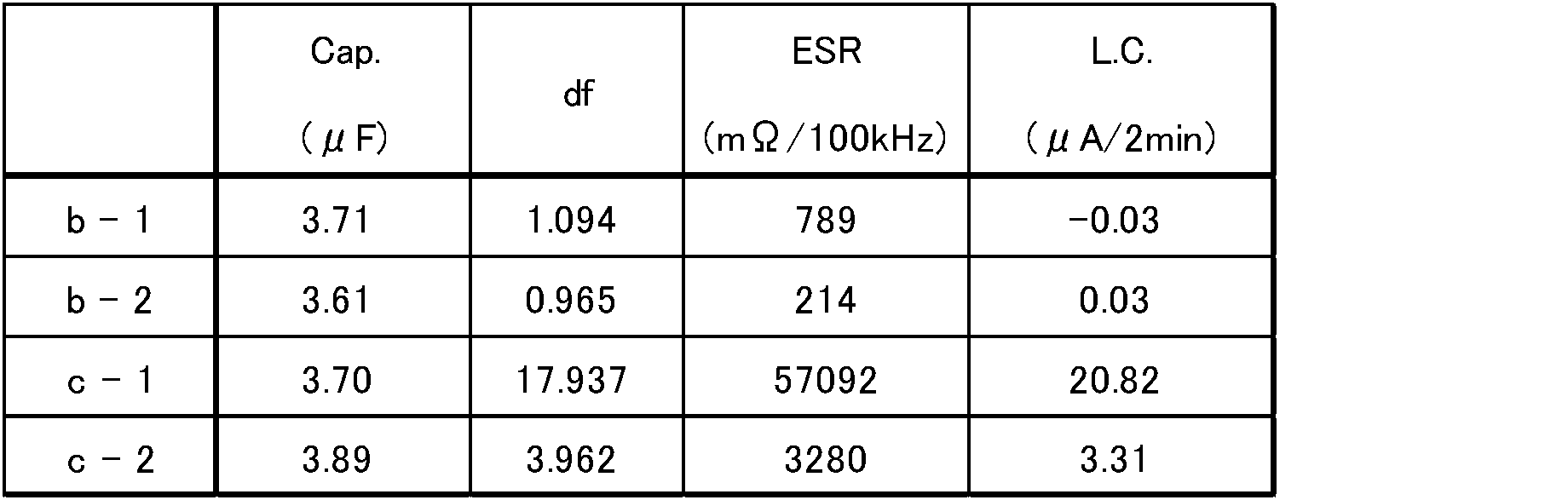
表4の結果より明らかなように、粗化処理することにより、ESRが低減し、誘電正接が低下している。
(実施例6)
表面の粗さを変化させた5枚の金属箔を用い、ユニットの積層数を2層とした他は、実施例1と同様にして5種類の固体電解コンデンサを製造し、実施例1と同様に、100kHzにおける等価直列抵抗(ESR)を測定した。その結果を表5に示す。
各種類の固体電解コンデンサについて10個ずつ製造、測定しており、測定値は10個の平均値である。
表面の粗さを変化させた5枚の金属箔を用い、ユニットの積層数を2層とした他は、実施例1と同様にして5種類の固体電解コンデンサを製造し、実施例1と同様に、100kHzにおける等価直列抵抗(ESR)を測定した。その結果を表5に示す。
各種類の固体電解コンデンサについて10個ずつ製造、測定しており、測定値は10個の平均値である。

表5の結果より明らかなように、金属箔のRaが30nm以上、1002nm以下の範囲内で、ESRが低減している。
(実施例7)
弁作用金属基体の陰極部側側面及び陰極部側端面に絶縁材料からなる絶縁部を形成し、固体電解質層が設けられている領域が弁作用金属基体の主面上で絶縁材料に囲まれている構造のユニットを作製し、実施例1と同様に積層体を作製して固体電解コンデンサを製造した。
この固体電解コンデンサ(4辺マスク構造)の漏れ電流を測定した結果を図7に示した。
図7には、比較のために、陽極部及び陰極部を分離するために周設された絶縁材料からなる絶縁層のみを有する構造(1辺マスク構造)の結果を合わせて示した。
漏れ電流は電圧印加後2分後の値とした。
図7には、10個の固体電解コンデンサについて漏れ電流の値を小さい順に下から上に向かってプロットしている。一番上(累積度数100%)に位置するプロットのLC値が一番大きい固体電解コンデンサの漏れ電流の値である。
この結果から、4辺マスク構造であるとLC不良を抑制することができることがわかる。
弁作用金属基体の陰極部側側面及び陰極部側端面に絶縁材料からなる絶縁部を形成し、固体電解質層が設けられている領域が弁作用金属基体の主面上で絶縁材料に囲まれている構造のユニットを作製し、実施例1と同様に積層体を作製して固体電解コンデンサを製造した。
この固体電解コンデンサ(4辺マスク構造)の漏れ電流を測定した結果を図7に示した。
図7には、比較のために、陽極部及び陰極部を分離するために周設された絶縁材料からなる絶縁層のみを有する構造(1辺マスク構造)の結果を合わせて示した。
漏れ電流は電圧印加後2分後の値とした。
図7には、10個の固体電解コンデンサについて漏れ電流の値を小さい順に下から上に向かってプロットしている。一番上(累積度数100%)に位置するプロットのLC値が一番大きい固体電解コンデンサの漏れ電流の値である。
この結果から、4辺マスク構造であるとLC不良を抑制することができることがわかる。
(実施例8)
直径11μm、30μm、99μm、250μm及び301μmの貫通孔が形成された金属箔を使用し、ユニットの積層数を2層とした他は、実施例1と同様にして5種類の固体電解コンデンサを製造し、実施例1と同様に、100kHzにおける等価直列抵抗(ESR)を測定した。その結果を表6に示す。
各種類の固体電解コンデンサについて10個ずつ製造、測定しており、測定値は10個の平均値である。
直径11μm、30μm、99μm、250μm及び301μmの貫通孔が形成された金属箔を使用し、ユニットの積層数を2層とした他は、実施例1と同様にして5種類の固体電解コンデンサを製造し、実施例1と同様に、100kHzにおける等価直列抵抗(ESR)を測定した。その結果を表6に示す。
各種類の固体電解コンデンサについて10個ずつ製造、測定しており、測定値は10個の平均値である。

表6の結果より明らかなように、金属箔に形成された貫通孔の直径が30μm以上、250μm以下の範囲内で、ESRが低減している。
1、1´、2 固体電解コンデンサ
10、40、50 ユニット
10b、40b ユニットの陰極部側端面
11 弁作用金属基体
11a 弁作用金属基体の陽極部側端面
11b 弁作用金属基体の陰極部側端面
11c 弁作用金属基体の陰極部側側面
12 金属芯部
13 多孔質層
14 誘電体層
15 固体電解質層
16 導電体層
16a カーボン層(導電体層)
16b 金属箔(導電体層)
16b1 金属箔
16b2 カーボンコート
16b3 カーボンコートされた金属箔
17 絶縁層
18 側面マスク部(絶縁部)
19 端面マスク部(絶縁部)
21 陽極部
22 陰極部
31 外装樹脂
32 陽極外部電極
33 陰極外部電極
10、40、50 ユニット
10b、40b ユニットの陰極部側端面
11 弁作用金属基体
11a 弁作用金属基体の陽極部側端面
11b 弁作用金属基体の陰極部側端面
11c 弁作用金属基体の陰極部側側面
12 金属芯部
13 多孔質層
14 誘電体層
15 固体電解質層
16 導電体層
16a カーボン層(導電体層)
16b 金属箔(導電体層)
16b1 金属箔
16b2 カーボンコート
16b3 カーボンコートされた金属箔
17 絶縁層
18 側面マスク部(絶縁部)
19 端面マスク部(絶縁部)
21 陽極部
22 陰極部
31 外装樹脂
32 陽極外部電極
33 陰極外部電極
Claims (21)
- 多孔質層を表面に有する弁作用金属基体と、
前記多孔質層の表面に形成された誘電体層と、
前記誘電体層上に設けられた固体電解質層とを有するユニットが複数個積層された固体電解コンデンサであって、
積層されたユニットの間に導電体層が存在し、前記導電体層のうち少なくとも一つは金属箔を含み、
前記ユニット及び前記導電体層は、外装樹脂により封止されており、
前記弁作用金属基体の陽極部側端面は、固体電解コンデンサの一端面において外装樹脂の表面に形成された陽極外部電極と直接接続されており、
前記金属箔は、固体電解コンデンサの他端面において外装樹脂の表面に形成された陰極外部電極と直接接続されていることを特徴とする固体電解コンデンサ。 - 前記金属箔を含む導電体層は、前記固体電解質層上に設けられたカーボン層と、表面にカーボンコートがされていない金属箔とからなり、前記金属箔が前記カーボン層と直接接している請求項1に記載の固体電解コンデンサ。
- 前記金属箔を含む導電体層は、前記固体電解質層上に設けられたカーボン層と、表面にカーボンコートされた金属箔とからなり、前記金属箔のカーボンコートされた表面が前記カーボン層と直接接している請求項1に記載の固体電解コンデンサ。
- 前記金属箔と前記カーボン層との間の接触抵抗は、前記カーボン層と前記固体電解質層との間の接触抵抗よりも小さい請求項2又は3に記載の固体電解コンデンサ。
- 前記金属箔と前記カーボン層との間の接触抵抗は、5mΩ以上、351mΩ以下である請求項2~4のいずれかに記載の固体電解コンデンサ。
- 前記金属箔を含む導電体層は、前記固体電解質層上に設けられたカーボン層と、前記カーボン層上に設けられた銀層と、前記銀層上に設けられた金属箔とからなる請求項1に記載の固体電解コンデンサ。
- 前記金属箔を含む導電体層は、前記金属箔のみからなり、前記金属箔は、前記固体電解質層と直接接している請求項1に記載の固体電解コンデンサ。
- 前記金属箔は、表面にカーボンコートされた金属箔であり、前記金属箔のカーボンコートされた表面が前記固体電解質層と直接接している請求項1に記載の固体電解コンデンサ。
- 前記金属箔を含む導電体層は、前記固体電解質層上に設けられた導電性接着剤層と、前記導電性接着剤層上に設けられた金属箔とからなる請求項1に記載の固体電解コンデンサ。
- 前記金属箔を含む導電体層は、前記固体電解質層上に設けられたカーボン層と、前記カーボン層上に設けられた導電性接着剤層と、前記導電性接着剤層上に設けられた金属箔とからなる請求項1に記載の固体電解コンデンサ。
- 積層されたユニットの間に存在する導電体層のうち、複数の導電体層が前記金属箔を含んでいる請求項1~10のいずれかに記載の固体電解コンデンサ。
- 積層されたユニットの間に存在する全ての前記導電体層が前記金属箔を含んでいる請求項1~11のいずれかに記載の固体電解コンデンサ。
- 前記金属箔の表面には粗化面が形成されている請求項1~12のいずれかに記載の固体電解コンデンサ。
- 前記金属箔の表面にはアンカーコート剤からなるコート層が形成されている請求項1~13のいずれかに記載の固体電解コンデンサ。
- 前記金属箔の表面粗さRaは、30nm以上、1002nm以下である請求項13又は14に記載の固体電解コンデンサ。
- 前記金属箔の厚さは、6μm以上、100μm以下である請求項1~15のいずれかに記載の固体電解コンデンサ。
- 前記金属箔の厚さ方向の抵抗値は、5mΩ以上、34mΩ以下である請求項1~16のいずれかに記載の固体電解コンデンサ。
- 前記金属箔は、アルミニウム、銅及び銀からなる群より選択される少なくとも一種の金属からなる請求項1~17のいずれかに記載の固体電解コンデンサ。
- 前記金属箔には、少なくとも1個の貫通孔が形成されている請求項1~18のいずれかに記載の固体電解コンデンサ。
- 前記弁作用金属基体には、陽極部及び陰極部を分離するために周設された、絶縁材料からなる絶縁層と、
弁作用金属基体の陰極部側側面及び陰極部側端面を覆う、絶縁材料からなる絶縁部とが形成されており、
前記固体電解質層が設けられている領域は弁作用金属基体の主面上で絶縁材料に囲まれている請求項1~19のいずれかに記載の固体電解コンデンサ。 - 複数の前記ユニットが積層されることにより形成された積層体の最下面と最上面には、前記金属箔が存在しない請求項1~20のいずれかに記載の固体電解コンデンサ。
Priority Applications (3)
| Application Number | Priority Date | Filing Date | Title |
|---|---|---|---|
| JP2018546318A JP6798560B2 (ja) | 2016-10-17 | 2017-10-16 | 固体電解コンデンサ |
| CN201780059768.8A CN109791844B (zh) | 2016-10-17 | 2017-10-16 | 固体电解电容器 |
| US16/384,028 US10991515B2 (en) | 2016-10-17 | 2019-04-15 | Solid electrolytic capacitor |
Applications Claiming Priority (2)
| Application Number | Priority Date | Filing Date | Title |
|---|---|---|---|
| JP2016-203682 | 2016-10-17 | ||
| JP2016203682 | 2016-10-17 |
Related Child Applications (1)
| Application Number | Title | Priority Date | Filing Date |
|---|---|---|---|
| US16/384,028 Continuation US10991515B2 (en) | 2016-10-17 | 2019-04-15 | Solid electrolytic capacitor |
Publications (1)
| Publication Number | Publication Date |
|---|---|
| WO2018074408A1 true WO2018074408A1 (ja) | 2018-04-26 |
Family
ID=62019489
Family Applications (1)
| Application Number | Title | Priority Date | Filing Date |
|---|---|---|---|
| PCT/JP2017/037334 Ceased WO2018074408A1 (ja) | 2016-10-17 | 2017-10-16 | 固体電解コンデンサ |
Country Status (4)
| Country | Link |
|---|---|
| US (1) | US10991515B2 (ja) |
| JP (1) | JP6798560B2 (ja) |
| CN (1) | CN109791844B (ja) |
| WO (1) | WO2018074408A1 (ja) |
Cited By (11)
| Publication number | Priority date | Publication date | Assignee | Title |
|---|---|---|---|---|
| JP2020107884A (ja) * | 2018-12-26 | 2020-07-09 | 株式会社村田製作所 | 電解コンデンサ |
| JP2020155695A (ja) * | 2019-03-22 | 2020-09-24 | 株式会社村田製作所 | 固体電解コンデンサ |
| CN111724993A (zh) * | 2019-03-22 | 2020-09-29 | 株式会社村田制作所 | 固体电解电容器 |
| JP2020167196A (ja) * | 2019-03-28 | 2020-10-08 | 株式会社村田製作所 | 固体電解コンデンサ、及び、固体電解コンデンサの製造方法 |
| WO2021049056A1 (ja) * | 2019-09-11 | 2021-03-18 | 株式会社村田製作所 | 電解コンデンサ |
| JPWO2021200197A1 (ja) * | 2020-03-31 | 2021-10-07 | ||
| JPWO2021256410A1 (ja) * | 2020-06-16 | 2021-12-23 | ||
| WO2022092010A1 (ja) * | 2020-10-30 | 2022-05-05 | パナソニックIpマネジメント株式会社 | 固体電解コンデンサ用のカーボンペースト、固体電解コンデンサ素子、および固体電解コンデンサ |
| WO2022131021A1 (ja) * | 2020-12-16 | 2022-06-23 | 株式会社村田製作所 | 電解コンデンサ及び電解コンデンサの製造方法 |
| JP2023043518A (ja) * | 2021-09-16 | 2023-03-29 | パナソニックホールディングス株式会社 | 固体電解コンデンサおよびその製造方法 |
| WO2023181745A1 (ja) * | 2022-03-24 | 2023-09-28 | パナソニックIpマネジメント株式会社 | 固体電解コンデンサ |
Families Citing this family (12)
| Publication number | Priority date | Publication date | Assignee | Title |
|---|---|---|---|---|
| JP7245997B2 (ja) * | 2017-10-31 | 2023-03-27 | パナソニックIpマネジメント株式会社 | 電解コンデンサおよびその製造方法 |
| CN111383844B (zh) * | 2018-12-26 | 2022-04-08 | 株式会社村田制作所 | 电解电容器 |
| JP7320742B2 (ja) * | 2019-04-22 | 2023-08-04 | パナソニックIpマネジメント株式会社 | 固体電解コンデンサ |
| US11170940B2 (en) * | 2019-05-17 | 2021-11-09 | Samsung Electro-Mechanics Co., Ltd. | Tantalum capacitor |
| US11515098B2 (en) | 2019-09-09 | 2022-11-29 | Murata Manufacturing Co., Ltd. | Solid electrolytic capacitor and method of producing solid electrolytic capacitor |
| US12198869B2 (en) * | 2019-10-31 | 2025-01-14 | Panasonic Intellectual Property Management Co., Ltd. | Electrolytic capacitor and manufacturing method thereof |
| JP7565949B2 (ja) * | 2020-01-09 | 2024-10-11 | 株式会社村田製作所 | 電解コンデンサ及び電解コンデンサの製造方法 |
| TWI756646B (zh) * | 2020-03-16 | 2022-03-01 | 鈺邦科技股份有限公司 | 電容器單元及其製造方法 |
| JP7756312B2 (ja) * | 2020-07-07 | 2025-10-20 | パナソニックIpマネジメント株式会社 | 固体電解コンデンサ素子、ならびに固体電解コンデンサおよびその製造方法 |
| US11923148B2 (en) * | 2022-04-18 | 2024-03-05 | Capxon Electronic Technology Co., Ltd. | Substrate-type multi-layer polymer capacitor (MLPC) having electroplated terminal structure |
| CN115475797B (zh) * | 2022-09-30 | 2024-04-05 | 肇庆绿宝石电子科技股份有限公司 | 一种叠层电容器及其制造方法、载条清洗液及制备方法 |
| TWI863370B (zh) * | 2023-06-20 | 2024-11-21 | 鈺邦科技股份有限公司 | 堆疊型電容器組件及其製作方法以及堆疊型電容器封裝結構 |
Citations (4)
| Publication number | Priority date | Publication date | Assignee | Title |
|---|---|---|---|---|
| JPH11219861A (ja) * | 1997-06-20 | 1999-08-10 | Matsushita Electric Ind Co Ltd | 電解コンデンサおよびその製造方法 |
| JP2002050545A (ja) * | 2000-08-04 | 2002-02-15 | Matsushita Electric Ind Co Ltd | チップ型積層コンデンサ |
| JP2009200370A (ja) * | 2008-02-25 | 2009-09-03 | Sanyo Electric Co Ltd | 固体電解コンデンサの製造方法 |
| JP2010199350A (ja) * | 2009-02-26 | 2010-09-09 | Nec Tokin Corp | 固体電解コンデンサ |
Family Cites Families (12)
| Publication number | Priority date | Publication date | Assignee | Title |
|---|---|---|---|---|
| JPH09312240A (ja) * | 1996-05-22 | 1997-12-02 | Nitsuko Corp | 積層型固体チップコンデンサ |
| DE69833149T2 (de) * | 1997-06-20 | 2006-09-07 | Matsushita Electric Industrial Co., Ltd., Kadoma | Elektrolytkondensator und dessen Herstellungsverfahren |
| JP3515698B2 (ja) * | 1998-02-09 | 2004-04-05 | 松下電器産業株式会社 | 4端子コンデンサ |
| TW516054B (en) * | 2000-05-26 | 2003-01-01 | Matsushita Electric Industrial Co Ltd | Solid electrolytic capacitor |
| US6504705B2 (en) * | 2000-10-12 | 2003-01-07 | Matsushita Electric Industrial Co., Ltd. | Electrolytic capacitor, circuit board containing electrolytic capacitor, and method for producing the same |
| US6563693B2 (en) * | 2001-07-02 | 2003-05-13 | Matsushita Electric Industrial Co., Ltd. | Solid electrolytic capacitor |
| JP2003133183A (ja) * | 2001-10-26 | 2003-05-09 | Matsushita Electric Ind Co Ltd | 固体電解コンデンサおよびその製造方法 |
| JP4739982B2 (ja) * | 2005-03-28 | 2011-08-03 | 三洋電機株式会社 | 固体電解コンデンサの製造方法 |
| WO2006106703A1 (ja) * | 2005-03-30 | 2006-10-12 | Showa Denko K. K. | 固体電解コンデンサ素子、その製造方法、及び固体電解コンデンサ |
| JP2008135427A (ja) | 2006-11-27 | 2008-06-12 | Matsushita Electric Ind Co Ltd | チップ形固体電解コンデンサの製造方法及びチップ形固体電解コンデンサ |
| TWI395243B (en) * | 2009-07-08 | 2013-05-01 | Stacked solid electrolytic condenser with positive multi-pin structure | |
| US8654511B2 (en) * | 2011-07-07 | 2014-02-18 | Apaq Technology Co., Ltd. | Capacitance unit and stacked solid electrolytic capacitor |
-
2017
- 2017-10-16 CN CN201780059768.8A patent/CN109791844B/zh active Active
- 2017-10-16 JP JP2018546318A patent/JP6798560B2/ja active Active
- 2017-10-16 WO PCT/JP2017/037334 patent/WO2018074408A1/ja not_active Ceased
-
2019
- 2019-04-15 US US16/384,028 patent/US10991515B2/en active Active
Patent Citations (4)
| Publication number | Priority date | Publication date | Assignee | Title |
|---|---|---|---|---|
| JPH11219861A (ja) * | 1997-06-20 | 1999-08-10 | Matsushita Electric Ind Co Ltd | 電解コンデンサおよびその製造方法 |
| JP2002050545A (ja) * | 2000-08-04 | 2002-02-15 | Matsushita Electric Ind Co Ltd | チップ型積層コンデンサ |
| JP2009200370A (ja) * | 2008-02-25 | 2009-09-03 | Sanyo Electric Co Ltd | 固体電解コンデンサの製造方法 |
| JP2010199350A (ja) * | 2009-02-26 | 2010-09-09 | Nec Tokin Corp | 固体電解コンデンサ |
Cited By (28)
| Publication number | Priority date | Publication date | Assignee | Title |
|---|---|---|---|---|
| JP2020107884A (ja) * | 2018-12-26 | 2020-07-09 | 株式会社村田製作所 | 電解コンデンサ |
| JP7200912B2 (ja) | 2018-12-26 | 2023-01-10 | 株式会社村田製作所 | 電解コンデンサ |
| US11232912B2 (en) | 2019-03-22 | 2022-01-25 | Murata Manufacturing Co., Ltd. | Solid electrolytic capacitor |
| JP2020155695A (ja) * | 2019-03-22 | 2020-09-24 | 株式会社村田製作所 | 固体電解コンデンサ |
| CN111724994A (zh) * | 2019-03-22 | 2020-09-29 | 株式会社村田制作所 | 固体电解电容器 |
| CN111724993A (zh) * | 2019-03-22 | 2020-09-29 | 株式会社村田制作所 | 固体电解电容器 |
| JP7067512B2 (ja) | 2019-03-22 | 2022-05-16 | 株式会社村田製作所 | 固体電解コンデンサ |
| US11170941B2 (en) | 2019-03-22 | 2021-11-09 | Murata Manufacturing Co., Ltd. | Solid electrolytic capacitor |
| JP2020167196A (ja) * | 2019-03-28 | 2020-10-08 | 株式会社村田製作所 | 固体電解コンデンサ、及び、固体電解コンデンサの製造方法 |
| JP7063301B2 (ja) | 2019-03-28 | 2022-05-09 | 株式会社村田製作所 | 固体電解コンデンサの製造方法 |
| US11881360B2 (en) | 2019-09-11 | 2024-01-23 | Murata Manufacturing Co., Ltd. | Electrolytic capacitor |
| WO2021049056A1 (ja) * | 2019-09-11 | 2021-03-18 | 株式会社村田製作所 | 電解コンデンサ |
| JPWO2021049056A1 (ja) * | 2019-09-11 | 2021-03-18 | ||
| JPWO2021200197A1 (ja) * | 2020-03-31 | 2021-10-07 | ||
| US12217916B2 (en) | 2020-06-16 | 2025-02-04 | Murata Manufacturing Co., Ltd. | Electronic component and method for manufacturing electronic component |
| WO2021256410A1 (ja) * | 2020-06-16 | 2021-12-23 | 株式会社村田製作所 | 電子部品及び電子部品の製造方法 |
| JPWO2021256410A1 (ja) * | 2020-06-16 | 2021-12-23 | ||
| JP7435775B2 (ja) | 2020-06-16 | 2024-02-21 | 株式会社村田製作所 | 電子部品及び電子部品の製造方法 |
| JPWO2022092010A1 (ja) * | 2020-10-30 | 2022-05-05 | ||
| US12562318B2 (en) | 2020-10-30 | 2026-02-24 | Panasonic Intellectual Property Management Co., Ltd. | Carbon paste for solid electrolytic capacitors, solid electrolytic capacitor element, and solid electrolytic capacitor |
| JP7724428B2 (ja) | 2020-10-30 | 2025-08-18 | パナソニックIpマネジメント株式会社 | 固体電解コンデンサ用のカーボンペースト、固体電解コンデンサ素子、および固体電解コンデンサ |
| WO2022092010A1 (ja) * | 2020-10-30 | 2022-05-05 | パナソニックIpマネジメント株式会社 | 固体電解コンデンサ用のカーボンペースト、固体電解コンデンサ素子、および固体電解コンデンサ |
| WO2022131021A1 (ja) * | 2020-12-16 | 2022-06-23 | 株式会社村田製作所 | 電解コンデンサ及び電解コンデンサの製造方法 |
| JP2023043518A (ja) * | 2021-09-16 | 2023-03-29 | パナソニックホールディングス株式会社 | 固体電解コンデンサおよびその製造方法 |
| JP7697852B2 (ja) | 2021-09-16 | 2025-06-24 | パナソニックホールディングス株式会社 | 固体電解コンデンサ |
| JPWO2023181745A1 (ja) * | 2022-03-24 | 2023-09-28 | ||
| JP7727956B2 (ja) | 2022-03-24 | 2025-08-22 | パナソニックIpマネジメント株式会社 | 固体電解コンデンサ |
| WO2023181745A1 (ja) * | 2022-03-24 | 2023-09-28 | パナソニックIpマネジメント株式会社 | 固体電解コンデンサ |
Also Published As
| Publication number | Publication date |
|---|---|
| JPWO2018074408A1 (ja) | 2019-06-24 |
| JP6798560B2 (ja) | 2020-12-09 |
| US10991515B2 (en) | 2021-04-27 |
| US20190244765A1 (en) | 2019-08-08 |
| CN109791844B (zh) | 2021-10-26 |
| CN109791844A (zh) | 2019-05-21 |
Similar Documents
| Publication | Publication Date | Title |
|---|---|---|
| JP6798560B2 (ja) | 固体電解コンデンサ | |
| JP6819691B2 (ja) | 固体電解コンデンサ及び固体電解コンデンサの製造方法 | |
| US20190122827A1 (en) | Method for producing solid electrolytic capacitor, and solid electrolytic capacitor | |
| JP2023027349A (ja) | 電解コンデンサの製造方法及び電解コンデンサ | |
| JP6856076B2 (ja) | 固体電解コンデンサ | |
| JP7259994B2 (ja) | 固体電解コンデンサ | |
| WO2018150886A1 (ja) | 固体電解コンデンサ及びその製造方法 | |
| JPWO2018066253A1 (ja) | 固体電解コンデンサ | |
| US20220223349A1 (en) | Electrolytic capacitor, and method for manufacturing electrolytic capacitor | |
| US11270846B2 (en) | Solid electrolytic capacitor and method for manufacturing solid electrolytic capacitor | |
| WO2021210367A1 (ja) | 電解コンデンサ及び電解コンデンサの製造方法 | |
| JP7375710B2 (ja) | 固体電解コンデンサ、及び、固体電解コンデンサの製造方法 | |
| JP7392379B2 (ja) | 固体電解コンデンサ | |
| US11984272B2 (en) | Solid electrolytic capacitor | |
| JP7400953B2 (ja) | 電解コンデンサ及び電解コンデンサの製造方法 | |
| CN112466667B (zh) | 固体电解电容器以及固体电解电容器的制造方法 | |
| JP7200912B2 (ja) | 電解コンデンサ | |
| JP7715203B2 (ja) | 電解コンデンサ素子 | |
| JP2007227716A (ja) | 積層型固体電解コンデンサおよびその製造方法 |
Legal Events
| Date | Code | Title | Description |
|---|---|---|---|
| 121 | Ep: the epo has been informed by wipo that ep was designated in this application |
Ref document number: 17862237 Country of ref document: EP Kind code of ref document: A1 |
|
| ENP | Entry into the national phase |
Ref document number: 2018546318 Country of ref document: JP Kind code of ref document: A |
|
| NENP | Non-entry into the national phase |
Ref country code: DE |
|
| 122 | Ep: pct application non-entry in european phase |
Ref document number: 17862237 Country of ref document: EP Kind code of ref document: A1 |