WO2018074322A1 - プラズマ処理装置及びプラズマ処理装置の制御方法 - Google Patents
プラズマ処理装置及びプラズマ処理装置の制御方法 Download PDFInfo
- Publication number
- WO2018074322A1 WO2018074322A1 PCT/JP2017/037016 JP2017037016W WO2018074322A1 WO 2018074322 A1 WO2018074322 A1 WO 2018074322A1 JP 2017037016 W JP2017037016 W JP 2017037016W WO 2018074322 A1 WO2018074322 A1 WO 2018074322A1
- Authority
- WO
- WIPO (PCT)
- Prior art keywords
- electrode
- processing apparatus
- plasma processing
- electrodes
- center
- Prior art date
- Legal status (The legal status is an assumption and is not a legal conclusion. Google has not performed a legal analysis and makes no representation as to the accuracy of the status listed.)
- Ceased
Links
Images



Classifications
-
- H—ELECTRICITY
- H01—ELECTRIC ELEMENTS
- H01J—ELECTRIC DISCHARGE TUBES OR DISCHARGE LAMPS
- H01J37/00—Discharge tubes with provision for introducing objects or material to be exposed to the discharge, e.g. for the purpose of examination or processing thereof
- H01J37/32—Gas-filled discharge tubes
- H01J37/32009—Arrangements for generation of plasma specially adapted for examination or treatment of objects, e.g. plasma sources
- H01J37/32082—Radio frequency generated discharge
- H01J37/32174—Circuits specially adapted for controlling the RF discharge
- H01J37/32183—Matching circuits
-
- H—ELECTRICITY
- H05—ELECTRIC TECHNIQUES NOT OTHERWISE PROVIDED FOR
- H05H—PLASMA TECHNIQUE; PRODUCTION OF ACCELERATED ELECTRICALLY-CHARGED PARTICLES OR OF NEUTRONS; PRODUCTION OR ACCELERATION OF NEUTRAL MOLECULAR OR ATOMIC BEAMS
- H05H1/00—Generating plasma; Handling plasma
- H05H1/24—Generating plasma
- H05H1/46—Generating plasma using applied electromagnetic fields, e.g. high frequency or microwave energy
-
- H—ELECTRICITY
- H01—ELECTRIC ELEMENTS
- H01J—ELECTRIC DISCHARGE TUBES OR DISCHARGE LAMPS
- H01J37/00—Discharge tubes with provision for introducing objects or material to be exposed to the discharge, e.g. for the purpose of examination or processing thereof
- H01J37/32—Gas-filled discharge tubes
- H01J37/32431—Constructional details of the reactor
- H01J37/32532—Electrodes
- H01J37/32541—Shape
-
- H—ELECTRICITY
- H01—ELECTRIC ELEMENTS
- H01J—ELECTRIC DISCHARGE TUBES OR DISCHARGE LAMPS
- H01J37/00—Discharge tubes with provision for introducing objects or material to be exposed to the discharge, e.g. for the purpose of examination or processing thereof
- H01J37/32—Gas-filled discharge tubes
- H01J37/32431—Constructional details of the reactor
- H01J37/32532—Electrodes
- H01J37/32577—Electrical connecting means
-
- H—ELECTRICITY
- H10—SEMICONDUCTOR DEVICES; ELECTRIC SOLID-STATE DEVICES NOT OTHERWISE PROVIDED FOR
- H10P—GENERIC PROCESSES OR APPARATUS FOR THE MANUFACTURE OR TREATMENT OF DEVICES COVERED BY CLASS H10
- H10P14/00—Formation of materials, e.g. in the shape of layers or pillars
- H10P14/60—Formation of materials, e.g. in the shape of layers or pillars of insulating materials
-
- H—ELECTRICITY
- H10—SEMICONDUCTOR DEVICES; ELECTRIC SOLID-STATE DEVICES NOT OTHERWISE PROVIDED FOR
- H10P—GENERIC PROCESSES OR APPARATUS FOR THE MANUFACTURE OR TREATMENT OF DEVICES COVERED BY CLASS H10
- H10P50/00—Etching of wafers, substrates or parts of devices
- H10P50/20—Dry etching; Plasma etching; Reactive-ion etching
- H10P50/24—Dry etching; Plasma etching; Reactive-ion etching of semiconductor materials
- H10P50/242—Dry etching; Plasma etching; Reactive-ion etching of semiconductor materials of Group IV materials
-
- H—ELECTRICITY
- H05—ELECTRIC TECHNIQUES NOT OTHERWISE PROVIDED FOR
- H05H—PLASMA TECHNIQUE; PRODUCTION OF ACCELERATED ELECTRICALLY-CHARGED PARTICLES OR OF NEUTRONS; PRODUCTION OR ACCELERATION OF NEUTRAL MOLECULAR OR ATOMIC BEAMS
- H05H2242/00—Auxiliary systems
- H05H2242/20—Power circuits
Definitions
- the present invention relates to a plasma processing apparatus that performs fine processing on an object to be processed with plasma and a control method for the plasma processing apparatus.
- plasma is used for thin film formation and / or etching.
- the plasma is generated, for example, by introducing a gas into a processing container and applying a high frequency of several MHz to several hundred MHz to an electrode provided in the processing container.
- the size of a silicon substrate used for manufacturing a semiconductor device tends to increase year by year, and mass production has already been performed on a silicon substrate having a diameter of 300 mm.
- VHF Very High Frequency
- a high frequency in the VHF (Very High Frequency) band of 30 to 300 MHz which is higher than the frequency of 13.56 MHz which is a frequency of a normal high frequency power source is used for plasma processing (for example, Patent Document 1, 2).
- the uniformity of plasma density may deteriorate due to the influence of standing waves generated by surface waves propagating on the surface of the electrode to which a high frequency is applied.
- the size of an electrode to which a high frequency is applied is larger than 1/20 of the wavelength in free space, it is difficult to excite highly uniform plasma unless some measures are taken.
- a uniform plasma can be obtained by setting the plasma excitation frequency to 13.56 MHz, but the plasma density is low and the electron temperature is high. It is difficult to form a high-quality thin film at high speed.
- the plasma excitation frequency is set to 100 MHz, which is approximately seven times, the film quality and the film forming speed are improved, but the processing uniformity is remarkably deteriorated.
- the uniformity may deteriorate under other process conditions.
- a high frequency application electrode larger than the substrate is provided on the opposite surface of the substrate.
- the high frequency current flows through the plasma between the high frequency application electrode and the ground such as the chamber wall and between the high frequency application electrode and the substrate.
- a standing wave is generated due to the influence of the surface wave propagating between the high-frequency applying electrode and the plasma, and it is difficult to generate a highly uniform plasma when a high plasma excitation frequency is used. It becomes.
- the plasma density distribution cannot be controlled.
- an object of the present invention is to provide an electrode for applying a high frequency and an electrode for connecting an impedance variable circuit, and changing the impedance of the electrode to change the high frequency between the electrodes or between the electrode and the ground.
- the plasma processing apparatus is a grounded processing container, a mounting table that supports an object to be processed inside the processing container, and a plurality of electrodes that are arranged to face the mounting table of the processing container, A plurality of electrodes insulated from each other and a high-frequency power supply for supplying high-frequency power for plasma generation, between two different electrodes among the plurality of electrodes, or with one electrode of the plurality of electrodes
- the high-frequency power source electrically connected to a container and an impedance variable circuit capable of controlling impedance, between two different electrodes among a plurality of electrodes, or one of a plurality of electrodes And an impedance variable circuit electrically connected between the electrode and the processing container.
- the plurality of electrodes includes a first electrode and a second electrode
- the high-frequency power source is electrically connected between the second electrode and the processing container
- the impedance variable circuit includes the first electrode It may be connected between the electrode and the processing container.
- the first electrode is a disc-shaped center electrode
- the second electrode is an annular electrode provided so as to surround the outer periphery of the center electrode
- the high-frequency power source is annularly connected via a matching unit. It may be electrically connected to the electrode and the processing container.
- the annular electrode and the center electrode are formed of a metal member, and an insulator member may be interposed between the annular electrode and the center electrode.
- the first coaxial pipe may further include one end of the inner conductor of the first coaxial pipe connected to the impedance variable circuit, and the other end of the inner conductor may be connected to the center electrode.
- the method further comprises a second coaxial waveguide including an inner conductor having a first portion and a plurality of second portions branched from the first portion, the end of the first portion being a matcher
- the ends of the plurality of second portions may be connected to the annular electrode at a position that is axially symmetric with respect to an axis passing through the center of the center electrode.
- the outer periphery of the object to be processed, the outer periphery of the surface facing the mounting table of the center electrode, the inner periphery of the surface facing the mounting table of the annular electrode, and the outer periphery of the surface facing the mounting table of the annular electrode are circular.
- the object to be processed, the center electrode and the annular electrode are: outer diameter of the surface facing the mounting table of the annular electrode> outer diameter of the object to be processed> inner diameter of the surface facing the mounting table of the annular electrode> mount of the center electrode You may have the relationship of the outer diameter of the surface which faces a mounting base.
- the plurality of electrodes includes a first electrode, a second electrode, and a third electrode
- the high frequency power source is electrically connected between the second electrode and the third electrode
- the impedance variable circuit may be electrically connected between the first electrode and the third electrode.
- the high-frequency power source is electrically connected between the second electrode and the third electrode via a matching device, and the third electrode is grounded via the matching device and the high-frequency power source. May be.
- a common mode choke may be provided in at least a part of the high-frequency transmission path that connects the high-frequency power source and the third electrode.
- the first electrode is a disc-shaped center electrode
- the second electrode is an annular electrode provided to surround the outer periphery of the center electrode
- the third electrode is an outer periphery of the annular electrode.
- the outer peripheral electrode provided so that it may surround may be sufficient.
- the center electrode, the annular electrode, and the outer peripheral electrode are formed of a metal member, and an insulator member may be interposed between the central electrode and the annular electrode and between the annular electrode and the outer peripheral electrode.
- the first coaxial pipe may further include one end of the inner conductor of the first coaxial pipe connected to the impedance variable circuit, and the other end of the inner conductor may be connected to the center electrode.
- the method further comprises a second coaxial waveguide including an inner conductor having a first portion and a plurality of second portions branched from the first portion, the end of the first portion being a matcher
- the ends of the plurality of second portions may be connected to the annular electrode at a position that is axially symmetric with respect to an axis passing through the center of the center electrode.
- the plurality of electrodes includes a first electrode and a second electrode
- the high-frequency power source is electrically connected between the first electrode and the second electrode
- the impedance variable circuit includes: The second electrode and the processing container may be electrically connected.
- the high-frequency power source may be electrically connected to the first electrode and the second electrode via a matching device, and the second electrode may be grounded via the matching device and the high-frequency power source.
- the first electrode may be a disk-shaped center electrode
- the second electrode may be an outer peripheral electrode provided so as to surround the outer periphery of the center electrode
- the center electrode and the outer peripheral electrode are formed of a metal member, and an insulator member may be interposed between the center electrode and the outer peripheral electrode.
- the first coaxial tube may further include one end of the inner conductor of the first coaxial tube connected to the matching unit, and the other end of the inner conductor may be connected to the center electrode.
- one end of the inner conductor of the first coaxial waveguide may be electrically short-circuited with the end of the outer conductor of the first coaxial waveguide.
- the apparatus may further include a second coaxial tube having one end electrically connected to the first coaxial tube and the other end electrically connected to the matching unit.
- the outer periphery of the object to be processed, the outer periphery of the surface facing the mounting table of the central electrode, the inner periphery of the surface facing the mounting table of the front outer peripheral electrode, and the outer periphery of the surface facing the mounting table of the outer peripheral electrode are
- the object to be processed, the center electrode, and the outer peripheral electrode are the outer diameter of the surface facing the mounting base of the outer peripheral electrode> the outer diameter of the target object> the inner diameter of the surface facing the mounting base of the outer peripheral electrode> the center electrode You may have the relationship of the outer diameter of the surface which faces a mounting base.
- the impedance variable circuit may be connected to the outer peripheral electrode at a plurality of positions that are axisymmetric with respect to an axis passing through the center of the center electrode.
- the end portions of the plurality of second portions may be connected to the annular electrode at equal intervals in the circumferential direction of the annular electrode.
- the annular electrode may be divided into a plurality of regions at equal intervals in the circumferential direction of the annular electrode.
- the processing container is grounded, the mounting table that supports the object to be processed inside the processing container, and the plurality of electrodes that are disposed to face the mounting table of the processing container, and are insulated from each other.
- a high-frequency power source for supplying a plurality of electrodes and a high-frequency power for generating plasma, between two different electrodes among the plurality of electrodes, or between one electrode of the plurality of electrodes and the processing vessel
- An impedance variable circuit that is electrically connected to the high-frequency power source and capable of controlling impedance, between two different electrodes among a plurality of electrodes, or one electrode of the plurality of electrodes and a processing container Measure the high-frequency amplitude or DC potential on the surface facing the mounting table of the variable impedance circuit electrically connected between the electrode and the one of the plurality of electrodes connected to the variable impedance circuit.
- the control method includes a step of acquiring a high frequency amplitude or a DC potential measured by a monitor, and a step of controlling the impedance of the impedance variable circuit so that the high frequency amplitude or the DC potential becomes a target value.
- the plasma density distribution can be controlled even when plasma is generated at a high excitation frequency.
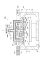
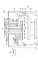
- FIG. 1 is a longitudinal sectional view of the plasma processing apparatus according to the first embodiment of the present invention
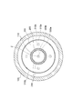
- FIG. 2 is a sectional view of the plasma processing apparatus along the line II-II in FIG.
- the plasma processing apparatus 10A shown in FIG. 1 includes a processing vessel 100, a mounting table 115, an upper electrode 212, an impedance variable circuit 400, and a high-frequency power source 505.
- the processing container 100 defines a processing space PS for plasma processing a target object (hereinafter referred to as a substrate W) such as a silicon substrate.
- the processing container 100 has a rectangular cross section, is formed of a metal such as an aluminum alloy, and is grounded.
- the processing container 100 includes a container body 105 and a lid 110.
- the container body 105 has a side wall and a bottom wall.
- the side wall of the container body 105 has a cylindrical shape.
- the lid 110 is attached to the container body 105 so as to close the upper opening of the container body 105.
- the lid 110 is grounded via the container body 105.
- An O-ring is provided between the container main body 105 and the lid 110 so that the airtightness in the processing container 100 is maintained.
- a mounting table 115 is disposed in the lower part of the processing container 100.
- a substrate W is supported on the upper surface of the mounting table 115.
- An exhaust port 120 is formed in the bottom wall of the processing container 100. The gas in the processing container 100 is exhausted from the exhaust port 120 by a vacuum pump (not shown).
- An upper electrode 212 is provided on the surface (ceiling surface) facing the substrate side surface of the processing container 100, that is, on the upper part of the processing container 100 so as to face the mounting table 115.
- the upper electrode 212 includes a center electrode 200 and an annular electrode 205 which are a plurality of electrodes.
- the center electrode 200 has a disk shape and is located at the center of the ceiling surface.
- the annular electrode 205 is annular and is provided so as to surround the outer periphery of the center electrode 200.
- the center electrode 200 and the annular electrode 205 are formed from a metal member.
- the outer peripheral surface and upper surface of the center electrode 200 are covered with an insulator member 210.
- the inner peripheral surface, the outer peripheral surface, and the upper surface of the annular electrode 205 are covered with an insulator member 210. That is, the insulator member 210 is interposed between the center electrode 200 and the annular electrode 205, and the center electrode 200 and the annular electrode 205 are insulated from each other by the insulator member 210.
- the insulator member 210 is made of a dielectric material such as alumina or quartz.
- the gas diffusion chamber 220 may be formed inside the center electrode 200, and the gas diffusion chamber 230 may be formed inside the annular electrode 205.
- a plurality of gas holes 220h communicating with the processing space PS extend downward from the gas diffusion chamber 220, and a plurality of gas holes 230h communicating with the processing space PS extend downward from the gas diffusion chamber 230.
- a first gas supply system 700 and a second gas supply system 710 are connected to the gas diffusion chamber 220 and the gas diffusion chamber 230 via gas supply pipes, respectively.
- the first gas supply system 700 and the second gas supply system 710 supply gas to the gas diffusion chamber 220 and the gas diffusion chamber 230, respectively, at a predetermined flow rate ratio.
- the gas supplied to the gas diffusion chamber 220 and the gas diffusion chamber 230 is distributed and supplied in a shower shape into the processing container 100 through the plurality of gas holes 220h and the plurality of gas holes 230h.
- the impedance variable circuit 400 is an electric circuit capable of controlling impedance, and is disposed between two different electrodes among the plurality of electrodes of the upper electrode 212 or one of the plurality of electrodes of the upper electrode 212 and a processing container. Is electrically connected between.
- the impedance variable circuit 400 has a first connection terminal 400a and a second connection terminal 400b.
- the first connection terminal 400a is electrically connected to the center electrode 200 via a line H1 and an internal conductor 300a described later
- the second connection terminal 400b is electrically connected to the lid 110 of the processing container 100 via a line G1. Connected. That is, the impedance variable circuit 400 is electrically connected between the center electrode 200 and the grounded processing container 100.
- FIG. 4 is a circuit diagram illustrating a configuration example of the impedance variable circuit 400.
- the variable impedance circuit 400 includes a variable capacitor only (400A), a variable capacitor and a coil connected in parallel (400B), and a variable capacitor and a coil connected in series (400C). Can be considered.
- the plasma processing apparatus 10A may further include a first coaxial waveguide 300.
- the first coaxial waveguide 300 is formed of an inner conductor 300a and an outer conductor 300b.
- the inner conductor 300 a extends so as to penetrate the lid 110 and the insulator member 210 of the processing container 100.
- One end of the inner conductor 300a is connected to the first connection terminal 400a of the impedance variable circuit 400 via a line H1.
- the other end of the inner conductor 300a is connected to the center electrode 200. According to this configuration, the impedance between the center electrode 200 and the ground can be changed by the impedance variable circuit 400 connected to the center electrode 200 and the ground plane of the processing container 100.
- the plasma processing apparatus 10A may further include a second coaxial waveguide 310.
- the second coaxial waveguide 310 includes an inner conductor 310a and an outer conductor 310b.
- the second coaxial waveguide 310 is branched into a plurality of coaxial waveguides at an intermediate position in the length direction.
- the second coaxial waveguide 310 is branched into four coaxial tubes. Note that the number of branches of the second coaxial waveguide 310 is not limited to four branches, and may be, for example, two branches, eight branches, or another number of branches.
- the inner conductor 310 a of the second coaxial waveguide 310 includes a first portion 312 and a plurality of second portions 314 branched from the first portion 312.
- An end portion of the first portion 312 of the inner conductor 310 a is connected to the high frequency power source 505 through the matching unit 500.
- the plurality of second portions 314 of the inner conductor 310 a extend so as to penetrate the processing container lid 110 and the insulator member 210, and their ends are connected to the annular electrode 205.
- the insulator member 210 is connected to a dielectric embedded between the inner conductor 300a and the outer conductor 300b or a dielectric embedded between the inner conductor 310a and the outer conductor 310b.
- the high-frequency power source 505 supplies high-frequency power for plasma generation, and between two different electrodes among the plurality of electrodes of the upper electrode 212 or one electrode of the plurality of electrodes of the upper electrode 212 It is electrically connected to the processing container 100.
- the high frequency power supply 505 includes a first power supply terminal 505a and a second power supply terminal 505b.
- the first power supply terminal 505a is electrically connected to the annular electrode 205 via the line H2 and the inner conductor 310a of the second coaxial waveguide 310.
- the second power supply terminal 505b is electrically connected to the lid 110 of the processing container 100 via the line G2 and the outer conductor 310b of the second coaxial waveguide 310. That is, the high frequency power source 505 is electrically connected between the annular electrode 205 and the grounded processing container 100.
- the center electrode 200 and the annular electrode 205 are separated by an insulator member 210.
- the other end of the first coaxial waveguide 300 is connected to the center position of the upper surface of the center electrode 200.
- the second coaxial waveguide 310 is arranged at an axially symmetric position with respect to an axis Z passing through the center of the center electrode 200.
- the plurality of ends of the second coaxial waveguide 310 may be connected to the annular electrode 205 at positions that are equally spaced in the circumferential direction of the annular electrode 205.
- the annular electrode 205 may be divided at equal intervals in the circumferential direction of the annular electrode 205.
- the annular electrode 205 is divided into four regions by the insulator member 210, and the end of the second coaxial waveguide 310 as a feeding point is connected to each region.
- the propagation distance of the surface wave propagating on the surface of the annular electrode 205 can be shortened, so that the occurrence of standing waves can be suppressed.
- the annular electrode 205 in the circumferential direction distortion due to thermal expansion can be absorbed, and the insulator member 210 can be prevented from cracking.
- the uniformity of plasma can be improved and the effect of preventing the insulator member 210 from cracking can be enhanced.
- the outer periphery of the substrate W, the outer periphery of the lower surface 200a that is the plasma exposure surface of the center electrode 200, the inner periphery of the lower surface 205a that is the plasma exposure surface of the annular electrode 205, and the outer periphery of the lower surface 205a of the annular electrode 205 are circular. is there. These sizes may have a relationship of the outer diameter of the lower surface 205a of the annular electrode 205> the outer diameter of the substrate W> the inner diameter of the lower surface 205a of the annular electrode 205> the outer diameter of the lower surface 200a of the center electrode 200.
- the lower surface 200a of the center electrode 200 and the lower surface 205a of the annular electrode 205 are surfaces facing the mounting table 115.
- the plasma processing apparatus 10A may include a monitor 600 and a control device 605.
- the monitor 600 is attached to a hot-side line H ⁇ b> 1 that connects the variable impedance circuit 400 and the center electrode 200.
- the monitor 600 measures the high frequency amplitude or DC potential of the lower surface 200a of the center electrode 200.
- the measured high frequency amplitude or DC potential is sent from the monitor 600 to the control device 605.
- the control device 605 includes, for example, a computer having a CPU, ROM, RAM, and I / F (InterFace) (not shown).
- the RAM of the control device 605 the target value of the high frequency amplitude or DC potential of the lower surface 200a of the center electrode 200 is stored in advance.
- the control device 605 acquires the measured value of the high frequency amplitude or DC potential, and controls the impedance of the impedance variable circuit 400 so that the high frequency amplitude or DC potential of the lower surface 200a of the center electrode 200 becomes a target value.
- the impedance of the variable impedance circuit 400 is feedback controlled even during the process.
- the high frequency output from the high frequency power source 505 is not applied between the substrate W and the upper electrode 212 but is applied between the annular electrode 205 and the lid 110 (ground), and the insulator member 210. Is output from. Part of the high frequency is consumed for plasma generation, and the other part of the high frequency returns to the insulator member 210 as a reflected wave.
- the high-frequency traveling wave and the reflected wave interfere with each other, and the electric field strength can be increased or decreased along the surface of the lower surface 200a of the electrode.
- the impedance between the center electrode 200 and the ground using the impedance variable circuit 400 connected between the center electrode 200 and the lid 110 (ground).
- the impedance between the center electrode 200 and the ground By changing the impedance between the center electrode 200 and the ground, the electric field strength and phase of the high frequency output from the insulator member 210 between the center electrode 200 and the annular electrode 205 can be changed. Thereby, the distribution of the electric field intensity of the center electrode 200 and the electric field intensity of the annular electrode 205 can be balanced, and the plasma density distribution can be controlled.
- the impedance control will be described more specifically.
- Lc be the inductance between the center electrode 200 and the ground
- Cs be the capacitance of the sheath formed between the center electrode 200 and the plasma.
- the inductance Lc is expressed by the following equation (1), As a result, the inductance Lc and the capacitance Cs are in series resonance.
- ⁇ is the plasma excitation angular frequency.
- the high-frequency current flows only between the annular electrode 205 and the center electrode 200 and does not flow into the ground plane. If the area of the lower surface 205a of the annular electrode 205 is larger than the area of the lower surface 200a of the center electrode 200, a higher voltage is applied to the sheath between the center electrode 200 and the plasma, and a higher density plasma is excited. That is, plasma having a higher density is generated in the central portion than in the peripheral portion of the substrate W.
- the reactance Xc between the center electrode 200 and the ground When the reactance Xc between the center electrode 200 and the ground is shifted from the resonance state to the positive side or the negative side, the impedance when the center electrode 200 is seen from the plasma increases, and the high-frequency current also flows through the ground plane.
- the reactance Xc between the center electrode 200 and the ground is infinite, that is, when the center electrode 200 is in a floating state, the high-frequency current does not flow through the center electrode 200 and flows only between the annular electrode 205 and the ground plane.
- the plasma since no high frequency voltage is applied to the sheath between the center electrode 200 and the plasma, the plasma is not excited on the front surface of the center electrode 200. That is, plasma having a higher density is generated in the peripheral portion than in the central portion of the substrate.
- the distribution of the plasma density can be controlled by changing the reactance of the variable impedance circuit 400 to change the reactance between the center electrode and the ground.
- a high-frequency current is allowed to flow between the annular electrode 205 and the ground instead of flowing a current between the substrate W and the upper electrode.
- an impedance variable circuit 400 is provided to control the impedance between the center electrode 200 and the ground.
- the upper electrode 212 includes a center electrode 200 and an annular electrode 205.
- the high frequency power source 505 may be connected between at least one first electrode of the plurality of electrodes and the ground of the processing container, and apply a high frequency.
- the impedance variable circuit 400 may be connected between at least one second electrode different from the first electrode among a plurality of electrodes and the ground of the processing container, and control the impedance.
- the center electrode 200 is an example of a first electrode included in the plurality of electrodes
- the annular electrode 205 is an example of a second electrode included in the plurality of electrodes.
- the plasma processing apparatus 10B according to the second embodiment is a modification of the plasma processing apparatus 10A according to the first embodiment, and the basic configuration is the same as that of the first embodiment.
- the configuration will be mainly described.
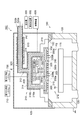
- the plasma processing apparatus 10B includes two second coaxial waveguides 316 instead of the second coaxial waveguide 310.
- the second coaxial waveguide 316 includes an inner conductor 316a and an outer conductor 316b. As shown in FIG. 5, one end of the inner conductor 316 a of the two second coaxial waveguides 316 is connected to the annular electrode 205.
- the plasma processing apparatus 10 ⁇ / b> B includes a two-output matching unit 510 instead of the matching unit 500.
- the 2-output matching unit 510 has a pair of input ports and two pairs of output ports.
- the high frequency power source 505 is connected to a pair of input ports of the two-output matching unit 510.
- the two-output matching unit 510 has both a branch function and a matching unit function. When the branch structure is present in the coaxial tube, the power distribution may be biased, whereas in the two-output matching unit 510, the power distribution bias can be reduced.
- the plasma processing apparatus 10 ⁇ / b> B further includes a shield 125 that is electrically connected to the lid 110.
- a line G2 connecting the two-output matching unit 510 and the second power supply terminal 505b of the high-frequency power source 505 is connected to the ground via the shield 125.
- the lid 110 is covered with a shield 125.
- the two-output matching unit 510, the impedance variable circuit 400, and the monitor 600 are disposed in the shield 125.
- the high frequency power source 505 is connected between the annular electrode 205 and the lid 110 (ground) via the two-output matching unit 510 and the two second coaxial pipes 316, and the high frequency power source 505 is connected between the annular electrode 205 and the lid 110. Electric power is applied.
- the shield 125 prevents high frequency from leaking outside the plasma processing apparatus 10B.
- a high-frequency current flows between the annular electrode 205 and the ground.
- the impedance variable circuit 400 controls the impedance between the center electrode 200 and the ground.
- the electric field strength and phase of the high frequency supplied into the processing container 100 from the insulator member 210 between the center electrode 200 and the annular electrode 205 can be changed.
- the distribution of the electric field intensity of the center electrode 200 and the electric field intensity of the annular electrode 205 can be balanced, and the plasma density distribution can be controlled.
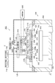
- the configuration of the plasma processing apparatus according to the third embodiment of the present invention will be described with reference to FIG.
- differences from the plasma processing apparatus 10A will be mainly described.
- the upper electrode 212 is divided into a center electrode 200, an annular electrode 205, and an outer peripheral electrode 215.
- the shapes and arrangement positions of the center electrode 200 and the annular electrode 205 are substantially the same as in the first embodiment.
- the outer peripheral electrode 215 is provided so as to surround the outer peripheral side of the annular electrode 205.
- the outer peripheral electrode 215 is formed at a position where the lid 110 is provided in the first and second embodiments.
- An insulating ring 122 is provided between the outer edge portion of the outer peripheral electrode 215 and the container main body 105, and the processing container 100 and the outer peripheral electrode 215 are insulated.
- a short-circuit portion P1 that electrically short-circuits between the outer peripheral electrode 215 and the matching unit 500 is provided between the outer peripheral electrode 215 and the ground.
- the outer peripheral electrode 215 is in a floating state in terms of electrical and high frequencies, but is connected to the ground in terms of transmission path (direct current).
- the center electrode 200, the annular electrode 205, and the outer peripheral electrode 215 are formed of a metal member. Insulator members 210 are interposed between the center electrode 200 and the annular electrode 205, and between the annular electrode 205 and the outer peripheral electrode 215, respectively.
- the central electrode 200, the annular electrode 205, and the outer peripheral electrode 215 are insulated from each other. Has been.
- one end of the inner conductor 300a of the first coaxial waveguide 300 is connected to the impedance variable circuit 400 through a line H1.
- the inner conductor 300 a of the first coaxial waveguide extends so as to penetrate the outer peripheral electrode 215 and the insulator member 210, and the other end of the first coaxial waveguide 300 is connected to the center electrode 200.
- the second coaxial waveguide 310 is branched into two coaxial waveguides at an intermediate position in the length direction.
- the number of branches of the second coaxial waveguide 310 is not limited to two branches, and may be, for example, four branches, eight branches, or another number of branches.
- the inner conductor 310 a of the second coaxial waveguide 310 includes a first portion 312 and two second portions 314 branched from the first portion 312.
- the two second portions 314 extend so as to penetrate the outer peripheral electrode 215 and the insulator member 210 and are connected to the annular electrode 205.
- These two second portions 314 are connected to the annular electrode 205 at an axially symmetric position with respect to an axis Z passing through the center of the center electrode 200.
- the upper end of the second coaxial waveguide 310 is connected to the third coaxial waveguide 320.
- the third coaxial waveguide 320 is connected to the high frequency power source 505 through the matching unit 500.
- the high frequency power source 505 is connected between the outer peripheral electrode 215 and the annular electrode 205 via the matching device 500 and applies a high frequency between the outer peripheral electrode 215 and the annular electrode 205. If a high-frequency current flows through the substrate W, the current flowing through the substrate W cannot be controlled independently. However, in this embodiment, a high-frequency current flows only between the electrodes, and no high-frequency current flows through the substrate W. This will be described.
- an annular ferrite 610 is provided in the vicinity of a part of the outer periphery of the third coaxial waveguide 320 in order to prevent a common mode from occurring and a high-frequency current from flowing to the ground side.
- the ferrite 610 functions as a common mode choke provided in at least a part of the high-frequency transmission path connecting the short-circuit portion P1 and the outer peripheral electrode 215. Since the permeability of ferrite is large, it acts as a large inductance for the common mode current flowing through the third coaxial waveguide 320. Thereby, the common mode current can be suppressed.
- the ferrite 610 on the third coaxial waveguide 320 in this way, it is possible to prevent a high frequency bias from being applied to the substrate W due to the high frequency applied to the annular electrode 205. As a result, the potential on the surface of the substrate W and the plasma density distribution can be controlled independently.
- the outer peripheral electrode 215 is grounded via the outer conductor 320 b of the third coaxial waveguide 320 that connects the outer peripheral electrode 215 and the matching unit 500. For this reason, at a high frequency, the impedance between the outer conductor 320b and the ground is increased to some extent. Therefore, it is not always necessary to provide a common mode choke.
- the impedance variable circuit 400 is connected between the outer peripheral electrode 215 and the center electrode 200, and controls the impedance between the outer peripheral electrode 215 and the central electrode 200.
- the monitor 600 is connected to the hot-side line H ⁇ b> 1 that connects the variable impedance circuit 400 and the center electrode 200.
- the monitor 600 measures the high frequency amplitude or DC potential of the lower surface 200 a of the center electrode 200 and sends the measured high frequency amplitude or DC potential to the control device 605.
- the control device 605 feedback-controls the impedance of the variable impedance circuit 400 based on the measured value of the high frequency amplitude or DC potential so that the high frequency amplitude or DC potential of the plasma exposed surface of the center electrode 200 becomes a target value.
- the balance of the high-frequency current flowing through the plasma on the surfaces of the center electrode 200, the annular electrode 205 and the outer peripheral electrode 215 is emitted between the central electrode 200 and the annular electrode 205 and between the annular electrode 205 and the outer peripheral electrode 215. It is determined by the phase difference and intensity difference of the surface wave propagating between each electrode and the plasma.
- the plasma processing apparatus 10C by changing the reactance of the variable impedance circuit 400, for example, only between the center electrode 200 and the annular electrode 205, only between the center electrode 200 and the outer peripheral electrode 215, or the annular electrode 205.
- a high-frequency current can be passed only between the outer peripheral electrode 215 and the outer peripheral electrode 215, or a high-frequency current can be passed between these electrodes at an arbitrary ratio.
- a high frequency current can be made to flow evenly through the three electrodes.
- the distribution of the plasma density in the radial direction of the substrate W can be freely controlled by changing the reactance of the variable impedance circuit 400 in this way.
- a high frequency is applied between the outer peripheral electrode 215 and the annular electrode 205 to control the impedance between the outer peripheral electrode 215 and the central electrode 200.
- the distribution of the electric field intensity of the center electrode 200 and the electric field intensity of the annular electrode 205 can be balanced, and the plasma density distribution can be controlled.
- the outer peripheral electrode 215 is in a floating state, high-frequency current is prevented from flowing to the ground side even if the impedance is variable. For this reason, the control of the impedance becomes easy and the accuracy of the control can be increased.
- the configuration in which the upper electrode 212 includes the three electrodes of the center electrode 200, the annular electrode 205, and the outer peripheral electrode 215 has been described.
- the center electrode 200 is an example of the first electrode
- the annular electrode 205 is an example of the second electrode
- the outer peripheral electrode 215 is only an example of the third electrode.
- the high frequency power source 505 may apply a high frequency between the third electrode and the second electrode
- the impedance variable circuit 400 may control the impedance between the third electrode and the first electrode. .
- the plasma processing apparatus 10D according to the fourth embodiment is a modification of the plasma processing apparatus 10C according to the third embodiment, and the basic configuration is the same as that of the third embodiment. Therefore, the configuration different from the plasma processing apparatus 10C is mainly described. Explained.
- the plasma processing apparatus 10D includes two second coaxial waveguides 316 instead of the second coaxial waveguide 310. As shown in FIG. 5, one end of the inner conductor 316 a of the two second coaxial waveguides 316 is connected to the annular electrode 205.
- the plasma processing apparatus 10 ⁇ / b> B includes a two-output matching unit 510 instead of the matching unit 500.
- the two-output matching unit 510 has a pair of input ports and two pairs of output ports.
- the high frequency power source 505 is connected to a pair of input ports of the two-output matching unit 510.
- Each of the two pairs of output ports is connected to the inner conductor 316 a and the outer peripheral electrode 215 of the second coaxial waveguide 316.
- the two-output matching unit 510 has both a branch function and a matching unit function. When a branch structure is added to the coaxial tube, the power distribution may be biased, whereas in the two-output matching unit 510, the power distribution bias can be reduced.
- a ferrite 610 is provided between the two-output matching unit 510 and the high-frequency power source 505.
- the plasma processing apparatus 10 ⁇ / b> D further includes a shield 125 that is electrically connected to the container body 105.
- a line G2 connecting the two-output matching unit 510 and the second power supply terminal 505b is connected to the ground via the shield 125.
- the outer peripheral electrode 215 is covered with a shield 125.
- the two-output matching unit 510, the impedance variable circuit 400, and the monitor 600 are disposed in the shield 125.
- the high frequency power source 505 is connected between the annular electrode 205 and the outer peripheral electrode 215 via the two-output matching unit 510 and the two second coaxial tubes 310, and the high frequency power is connected between the annular electrode 205 and the outer peripheral electrode 215. Is applied.
- the shield 125 prevents high frequency from leaking outside the plasma processing apparatus 10D.
- the high frequency power is applied between the annular electrode 205 and the outer peripheral electrode 215, and the impedance between the center electrode 200 and the outer peripheral electrode 215.
- the flow of the high-frequency current between the electrodes can be controlled to control the plasma density distribution.
- the configuration of a plasma processing apparatus according to the fifth embodiment of the present invention will be described with reference to FIG. below, it demonstrates centering on a different point from the above-mentioned plasma processing apparatus.
- the upper electrode 212 is divided into two, a center electrode 200 and an outer peripheral electrode 215.
- the center electrode 200 and the outer peripheral electrode 215 are insulated via an insulator member 210.
- the plasma processing apparatus 10E includes a first coaxial waveguide 300.
- One end of the inner conductor 300 a of the first coaxial waveguide 300 is connected to the matching unit 500.
- the inner conductor 300 a of the first coaxial waveguide 300 extends so as to penetrate the outer peripheral electrode 215 and the insulator member 210, and the other end of the inner conductor 300 a is connected to the center electrode 200.
- the outer conductor 300 b of the first coaxial waveguide 300 is connected to the outer peripheral electrode 215.
- An insulating ring 122 is provided between the outer edge of the outer peripheral electrode 215 and the container main body 105, and the processing container 100 and the outer peripheral electrode 215 are insulated.
- the outer peripheral electrode 215 is in a floating state in terms of electrical and high frequencies, but is connected to the ground in terms of transmission path (direct current).
- O-rings 140 and 145 are provided above and below the insulating ring 122, and the insulating ring 122 and the O-rings 140 and 145 are crushed by the insulator presser 150, so that processing in the processing container 100 is performed from the atmospheric space above the outer peripheral electrode 215.
- the space PS is sealed.
- the outer periphery of the substrate W, the outer periphery of the lower surface 200a of the center electrode 200, the inner periphery of the lower surface 215a of the outer peripheral electrode 215, and the outer periphery of the lower surface 215a of the outer peripheral electrode 215 are circular.
- the first gas supply system 700 introduces the first gas into the gas supply pipe 705 that penetrates the upper cover 130.
- the introduced first gas is formed inside the outer peripheral electrode 215, flows through the gas passage 250 a communicating with the gas supply pipe 705, and is supplied into the processing container 100 from the first gas hole 250 b.
- the second gas supply system 710 introduces the second gas into the gas passage 240a formed in the inner conductor 300a of the first coaxial waveguide. The second gas is supplied into the processing container from the second gas hole 240b.
- the refrigerant supply system 720 supplies the refrigerant to the refrigerant supply pipe 725.
- the supplied refrigerant communicates with the refrigerant supply pipe 725 and flows through an annular refrigerant passage 250 c formed inside the outer peripheral electrode 215, thereby adjusting the temperature of the outer peripheral electrode 215.
- the plasma processing apparatuses 10A, 10B, 10C, and 10D described above do not include the refrigerant supply system 720, the refrigerant supply system 720 can also be applied to the plasma processing apparatuses 10A, 10B, 10C, and 10D.
- the high-frequency power source 505 of the plasma processing apparatus 10 ⁇ / b> E is connected between the outer peripheral electrode 215 and the central electrode 200 via the matching unit 500, and allows a high-frequency current to flow between the outer peripheral electrode 215 and the central electrode 200.
- a short-circuit portion P2 for electrically short-circuiting the outer peripheral electrode 215 and the matching unit 500 is provided between the outer peripheral electrode 215 and the processing container 100. Note that a short-circuit portion that electrically short-circuits between the matching unit 500 and the high-frequency power source 505 may be provided between the outer peripheral electrode 215 and the processing container 100.
- the impedance variable circuit 400 of the plasma processing apparatus 10E is connected between the outer peripheral electrode 215 and the grounded processing container 100 so as to control the impedance. Although only one impedance variable circuit 400 is illustrated in FIG. 8, in one embodiment, the plurality of impedance variable circuits 400 are arranged at positions that are axially symmetric with respect to an axis Z passing through the center of the center electrode 200. 215 and the processing container 100 may be connected.
- the outer peripheral electrode 215 is grounded via the outer conductor 300b that connects the outer peripheral electrode 215 and the matching unit 500. For this reason, at a high frequency, the impedance between the external conductor 300b and the ground is somewhat high. Therefore, if the impedance of the variable impedance circuit 400 is high, most of the high-frequency current flows between the center electrode 200 and the outer peripheral electrode 215 and hardly flows on the ground plane. If the areas of the lower surfaces of the center electrode 200 and the outer peripheral electrode 215 are substantially equal, substantially equal high frequency voltages are applied to the sheath between the central electrode 200 and the plasma and the sheath between the outer peripheral electrode 215 and the plasma.
- a high-frequency current flows only between the outer peripheral electrode 215 and the center electrode 200 and does not flow to the ground.
- the reactance of the variable impedance circuit 400 is set to a finite value, a high-frequency current also flows through the ground plane according to the reactance. If a high-frequency current having the same phase as that of the outer peripheral electrode 215 flows on the ground plane, the high-frequency current flowing through the center electrode 200 increases, so that high-density plasma is excited below the center electrode 200. Conversely, if a high-frequency current having the same phase as that of the center electrode 200 flows on the ground plane, the high-frequency current flowing through the outer peripheral electrode 215 increases, so that high density plasma is excited below the outer peripheral electrode 215.
- control device 605 can freely control the distribution of the plasma density in the radial direction of the substrate W by controlling the reactance of the impedance variable circuit 400 based on the measurement value of the monitor 600.
- the number of electrodes can be reduced as compared with the third and fourth embodiments, and the structure can be simplified because branching can be eliminated. An effect is also obtained.
- the configuration including the center electrode 200 and the outer peripheral electrode 215 has been described.
- the center electrode 200 is an example of the first electrode among the first electrode and the second electrode arranged to be insulated from each other on the surface facing the mounting table of the processing container
- the outer peripheral electrode 215 is It is only an example of the second electrode.
- the plasma processing apparatus 10F according to the sixth embodiment is a modification of the plasma processing apparatus 10E according to the fifth embodiment, and the basic configuration is the same as that of the fifth embodiment. Therefore, the configuration different from the plasma processing apparatus 10E is mainly described. Explained.
- a short-circuit portion P3 that electrically short-circuits the outer conductor 300b and the inner conductor 300a of the first coaxial waveguide 300 is provided.
- the center electrode 200 is grounded via the inner conductor 300a and the outer conductor 300b.
- the second coaxial pipe 310 is connected to the first coaxial waveguide 300 at one end and to the matching unit 500 at the other end.
- the second coaxial waveguide 310 is connected to the first coaxial waveguide 300 by a metal member 310c that couples the internal conductor 310a and the internal conductor 300a, and supplies power from the middle sidewall of the first coaxial waveguide 300. .
- the gas supply system 715 causes a gas to flow through the gas passage 240a formed inside the first coaxial waveguide 300 and supplies the gas into the processing container through the gas hole 240b.
- the refrigerant supply system 720 adjusts the temperatures of the center electrode 200 and the outer peripheral electrode 215 by flowing the refrigerant through the refrigerant passage 240c formed in the inner conductor 300a and the refrigerant passage 250c formed in the outer conductor 300b.
- the configuration of the gas supply system 715 and the refrigerant supply system 720 can be simplified.
- the plasma processing apparatuses 10A, 10B, 10C, and 10D described above do not include the refrigerant supply system 720, the refrigerant supply system 720 can also be applied to the plasma processing apparatuses 10A, 10B, 10C, and 10D.
- the plasma density distribution in the radial direction of the substrate W can be freely controlled by variably controlling the reactance of the impedance variable circuit 400. Can do. Further, in the plasma processing apparatus 10F according to the present embodiment, the number of electrodes can be reduced as compared with the third and fourth embodiments, and the branch can be eliminated, so that the structure can be simplified. .
- the electrodes for applying the high frequency and the electrodes for connecting the impedance variable circuit are provided, and the impedance of the electrodes is changed to change the distance between the electrodes or the electrodes.
- the plasma density distribution can be controlled by changing the flow of the high-frequency current between the grounds. That is, by controlling the impedance between two different electrodes to which the impedance variable circuit is connected, or between one electrode and the processing container, the intensity and phase of the high-frequency wave propagating on the surface of the electrode can be changed. it can. As a result, the distribution of standing waves on the surface of the electrode can be changed, and the distribution of plasma density can be controlled.
- the plasma processing apparatus according to the present invention is mainly used as a semiconductor manufacturing apparatus, but may be used in a substrate processing apparatus.
- a substrate processing apparatus For example, it can be used for a flat panel display manufacturing process and a solar cell manufacturing process in addition to a semiconductor manufacturing process. Therefore, the object to be processed is not limited to a silicon substrate, and may be a glass substrate.
- the upper electrode 212 can have any number of electrodes as long as it includes a plurality of electrodes.
- the high frequency power source 505 is electrically connected between two different electrodes of the plurality of electrodes of the upper electrode 212 or between one electrode of the plurality of electrodes of the upper electrode 212 and the processing vessel 100. It only has to be done.
- the impedance variable circuit 400 is electrically connected between two different electrodes among the plurality of electrodes of the upper electrode 212 or between one electrode of the plurality of electrodes of the upper electrode 212 and the processing container. It only has to be done. If such a configuration is provided, the intensity and phase of the high-frequency wave propagating on the surface of the electrode can be changed by controlling the impedance of the impedance variable circuit. As a result, the distribution of standing waves on the surface of the electrode can be changed, and the distribution of plasma density can be controlled.
- 10A, 10B, 10C, 10D, 10E, 10F Plasma processing apparatus, 100 ... Processing vessel, 115 ... Mounting table, 200 ... Center electrode, 205 ... Ring electrode, 210 ... Insulator member, 212 ... Upper electrode, 215 ... Outer periphery Electrode, 300 ... first coaxial tube, 300a ... inner conductor, 300b ... outer conductor, 310 ... second coaxial tube, 310a ... inner conductor, 310b ... outer conductor, 312 ... first part, 314 ... second 316 ... second coaxial tube, 316a ... inner conductor, 320 ... third coaxial tube, 320b ... outer conductor, 400 ... impedance variable circuit, 500 ... matching device, 505 ... high frequency power supply, 510 ... two output matching device , 600, monitor, 605, control device, 610, ferrite, P1, P2, P3, short-circuit portion, W, substrate, Z, axis.
Landscapes
- Physics & Mathematics (AREA)
- Engineering & Computer Science (AREA)
- Plasma & Fusion (AREA)
- Chemical & Material Sciences (AREA)
- Analytical Chemistry (AREA)
- Electromagnetism (AREA)
- Spectroscopy & Molecular Physics (AREA)
- Plasma Technology (AREA)
- Drying Of Semiconductors (AREA)
- Chemical Vapour Deposition (AREA)
Abstract
Description
[プラズマ処理装置の構成]
まず、本発明の第1実施形態に係るプラズマ処理装置の構成について図1及び図2を参照しながら説明する。図1は本発明の第1実施形態に係るプラズマ処理装置の縦断面図であり、図2は図1のII-II線に沿ったプラズマ処理装置の断面図である。
次に、本実施形態に係るプラズマ処理装置10Aの制御方法について説明する。本実施形態では、プラズマ処理装置10Aはモニタ600及び制御装置605を備え得る。モニタ600は、インピーダンス可変回路400と中心電極200とをつなぐホット側の線H1に取り付けられている。モニタ600は、中心電極200の下面200aの高周波振幅または直流電位が測定する。測定された高周波振幅または直流電位は、モニタ600から制御装置605に送られる。

[プラズマ処理装置の構成]
次に、本発明の第2実施形態に係るプラズマ処理装置の構成について図5を参照しながら説明する。第2実施形態に係るプラズマ処理装置10Bは第1実施形態に係るプラズマ処理装置10Aの変形例であり、基本的構成は第1実施形態と同じであるため、以下では、プラズマ処理装置10Aと異なる構成について主に説明する。
[プラズマ処理装置の構成]
次に、本発明の第3実施形態に係るプラズマ処理装置の構成について図6を参照しながら説明する。以下では、プラズマ処理装置10Aと異なる点について主に説明する。第3実施形態に係るプラズマ処理装置10Cでは、上部電極212が、中心電極200、環状電極205及び外周電極215の3つに分かれている。中心電極200及び環状電極205の形状及び配置位置は第1実施形態とほぼ同じである。外周電極215は、環状電極205の外周側を取り囲むように設けられている。
[プラズマ処理装置の構成]
次に、本発明の第4実施形態に係るプラズマ処理装置の構成について図7を参照しながら説明する。第4実施形態に係るプラズマ処理装置10Dは第3実施形態に係るプラズマ処理装置10Cの変形例であり、基本的構成は第3実施形態と同じであるため、プラズマ処理装置10Cと異なる構成について中心に説明する。
[プラズマ処理装置の構成]
次に、本発明の第5実施形態に係るプラズマ処理装置の構成について図8を参照しながら説明する。以下では、上述のプラズマ処理装置と異なる点について中心に説明する。第5実施形態に係るプラズマ処理装置10Eでは、上部電極212が、中心電極200及び外周電極215の2つに分かれている。中心電極200と外周電極215との間は、絶縁体部材210を介して絶縁されている。
[プラズマ処理装置の構成]
次に、本発明の第6実施形態に係るプラズマ処理装置の構成について図9を参照しながら説明する。第6実施形態に係るプラズマ処理装置10Fは第5実施形態に係るプラズマ処理装置10Eの変形例であり、基本的構成は第5実施形態と同じであるため、プラズマ処理装置10Eと異なる構成について中心に説明する。
Claims (26)
- 接地された処理容器と、
前記処理容器の内部にて被処理体を支持する載置台と、
前記処理容器の前記載置台と対面するように配置された複数の電極であり、互いに絶縁された、該複数の電極と、
プラズマ生成用の高周波電力を供給する高周波電源であり、前記複数の電極のうち異なる2つの電極の間、又は、前記複数の電極のうちの1つの電極と前記処理容器との間に電気的に接続された、該高周波電源と、
インピーダンスを制御可能なインピーダンス可変回路であり、前記複数の電極のうち異なる2つの電極の間、又は、前記複数の電極のうちの1つの電極と前記処理容器との間に電気的に接続された、該インピーダンス可変回路と、を備える、プラズマ処理装置。 - 前記複数の電極は、第1の電極及び第2の電極を含み、
前記高周波電源は、前記第2の電極と前記処理容器との間に電気的に接続され、
前記インピーダンス可変回路は、前記第1の電極と前記処理容器との間に接続された、請求項1に記載のプラズマ処理装置。 - 前記第1の電極は円盤状の中心電極であり、前記第2の電極は該中心電極の外周を囲むように設けられた環状電極であり、
前記高周波電源は、整合器を介して前記環状電極及び前記処理容器に電気的に接続されている、請求項2に記載のプラズマ処理装置。 - 前記環状電極及び前記中心電極は、金属部材から形成され、前記環状電極と前記中心電極との間には絶縁体部材が介在している、請求項3に記載のプラズマ処理装置。
- 第1の同軸管を更に備え、
前記第1の同軸管の内部導体の一端は前記インピーダンス可変回路に接続され、該内部導体の他端は前記中心電極に接続されている、請求項3又は4に記載のプラズマ処理装置。 - 第1の部分と該第1の部分から分岐した複数の第2の部分とを有する内部導体を含む第2の同軸管を更に備え、
前記第1の部分の端部は前記整合器に接続され、前記複数の第2の部分の端部は前記中心電極の中心を通る軸線に対して軸対称となる位置で前記環状電極に接続されている、請求項3~5のいずれか一項に記載のプラズマ処理装置。 - 前記被処理体の外周、前記中心電極の前記載置台と対面する面の外周、前記環状電極の前記載置台と対面する面の内周、及び前記環状電極の前記載置台と対面する面の外周は円形であり、
前記被処理体、前記中心電極及び前記環状電極は、
前記環状電極の前記載置台と対面する面の外径>前記被処理体の外径>前記環状電極の前記載置台と対面する面の内径>前記中心電極の前記載置台と対面する面の外径
の関係を有する、請求項3~6のいずれか一項に記載のプラズマ処理装置。 - 前記複数の電極は、第1の電極、第2の電極及び第3の電極を含み、
前記高周波電源は、前記第2の電極と前記第3の電極との間に電気的に接続され、
前記インピーダンス可変回路は、前記第1の電極と前記第3の電極との間に電気的に接続されている、請求項1に記載のプラズマ処理装置。 - 前記高周波電源は、前記第2の電極と前記第3の電極との間に整合器を介して電気的に接続され、
前記第3の電極は、前記整合器及び前記高周波電源を介して接地されている、請求項8に記載のプラズマ処理装置。 - 前記高周波電源と前記第3の電極とを接続する高周波伝送路の少なくとも一部にコモンモードチョークが設けられている、請求項9に記載のプラズマ処理装置。
- 前記第1の電極は円盤状の中心電極であり、
前記第2の電極は該中心電極の外周を取り囲むように設けられた環状電極であり、
前記第3の電極は前記環状電極の外周を取り囲むように設けられた外周電極である、請求項9又は10に記載のプラズマ処理装置。 - 前記中心電極、前記環状電極及び前記外周電極は、金属部材から形成され、
前記中心電極と前記環状電極との間及び前記環状電極と前記外周電極との間には絶縁体部材が介在している、請求項11に記載のプラズマ処理装置。 - 第1の同軸管を更に備え、
前記第1の同軸管の内部導体の一端は前記インピーダンス可変回路に接続され、該内部導体の他端は前記中心電極に接続されている、請求項11又は12に記載のプラズマ処理装置。 - 第1の部分と該第1の部分から分岐した複数の第2の部分とを有する内部導体を含む第2の同軸管を更に備え、
前記第1の部分の端部は前記整合器に接続され、前記複数の第2の部分の端部は前記中心電極の中心を通る軸線に対して軸対称となる位置で前記環状電極に接続されている、請求項11~13のいずれか一項に記載のプラズマ処理装置。 - 前記複数の電極は、第1の電極及び第2の電極を含み、
前記高周波電源は、前記第1の電極と前記第2の電極との間に電気的に接続され、
前記インピーダンス可変回路は、前記第2の電極と前記処理容器との間に電気的に接続されている、
請求項1に記載のプラズマ処理装置。 - 前記高周波電源は、整合器を介して前記第1の電極及び前記第2の電極に電気的に接続され、
前記第2の電極は、前記整合器及び前記高周波電源を介して接地されている、請求項15に記載のプラズマ処理装置。 - 前記第1の電極は円盤状の中心電極であり、
前記第2の電極は前記中心電極の外周を取り囲むように設けられた外周電極である、請求項16に記載のプラズマ処理装置。 - 前記中心電極及び前記外周電極は、金属部材から形成され、
前記中心電極と前記外周電極との間には、絶縁体部材が介在している、請求項17に記載のプラズマ処理装置。 - 第1の同軸管を更に備え、
前記第1の同軸管の内部導体の一端は前記整合器に接続され、該内部導体の他端は前記中心電極に接続されている、請求項17又は18に記載のプラズマ処理装置。 - 前記第1の同軸管の内部導体の一端は、前記第1の同軸管の外部導体の端部と電気的に短絡されている、請求項19に記載のプラズマ処理装置。
- 一端が前記第1の同軸管に電気的に接続され、他端が前記整合器に電気的に接続された第2の同軸管を更に備える、請求項19又は20に記載のプラズマ処理装置。
- 前記被処理体の外周、前記中心電極の前記載置台と対面する面の外周、前記外周電極の前記載置台と対面する面の内周、及び前記外周電極の前記載置台と対面する面の外周は円形であり、
前記被処理体、前記中心電極及び前記外周電極は、
前記外周電極の前記載置台と対面する面の外径>前記被処理体の外径>前記外周電極の前記載置台と対面する面の内径>前記中心電極の前記載置台と対面する面の外径
の関係を有する、請求項17~21のいずれか一項に記載のプラズマ処理装置。 - 前記インピーダンス可変回路は、前記中心電極の中心を通る軸線に対して軸対称な複数の位置で前記外周電極に接続されている、請求項17~22のいずれか一項に記載のプラズマ処理装置。
- 前記複数の第2の部分の端部は、前記環状電極の周方向において等間隔となる位置で前記環状電極に接続されている、請求項6又は14に記載のプラズマ処理装置。
- 前記環状電極は、前記環状電極の周方向に等しい間隔で複数の領域に分割されている、請求項3~7、11~14のいずれか一項に記載のプラズマ処理装置。
- 接地された処理容器と、
前記処理容器の内部にて被処理体を支持する載置台と、
前記処理容器の前記載置台と対面するように配置された複数の電極であり、互いに絶縁された、該複数の電極と、
プラズマ生成用の高周波電力を供給する高周波電源であり、前記複数の電極のうち異なる2つの電極の間、又は、前記複数の電極のうちの1つの電極と前記処理容器との間に電気的に接続された、該高周波電源と、
インピーダンスを制御可能なインピーダンス可変回路であり、前記複数の電極のうち異なる2つの電極の間、又は、前記複数の電極のうちの1つの電極と前記処理容器との間に電気的に接続された、該インピーダンス可変回路と、
前記複数の電極のうち前記インピーダンス可変回路に接続する1つの電極の前記載置台と対面する面における高周波振幅または直流電位を測定するためのモニタと、を備えるプラズマ処理装置の制御方法であって、
前記モニタによって測定された前記高周波振幅又は直流電位を取得するステップと、
前記高周波振幅又は直流電位が目標値になるように前記インピーダンス可変回路のインピーダンスを制御するステップと、を含む、プラズマ処理装置の制御方法。
Priority Applications (3)
| Application Number | Priority Date | Filing Date | Title |
|---|---|---|---|
| KR1020197012129A KR102194176B1 (ko) | 2016-10-19 | 2017-10-12 | 플라스마 처리 장치 및 플라스마 처리 장치의 제어 방법 |
| JP2018546281A JP6819968B2 (ja) | 2016-10-19 | 2017-10-12 | プラズマ処理装置 |
| US16/343,322 US10674595B2 (en) | 2016-10-19 | 2017-10-12 | Plasma processing apparatus and method for controlling plasma processing apparatus |
Applications Claiming Priority (2)
| Application Number | Priority Date | Filing Date | Title |
|---|---|---|---|
| JP2016205289 | 2016-10-19 | ||
| JP2016-205289 | 2016-10-19 |
Publications (1)
| Publication Number | Publication Date |
|---|---|
| WO2018074322A1 true WO2018074322A1 (ja) | 2018-04-26 |
Family
ID=62018517
Family Applications (1)
| Application Number | Title | Priority Date | Filing Date |
|---|---|---|---|
| PCT/JP2017/037016 Ceased WO2018074322A1 (ja) | 2016-10-19 | 2017-10-12 | プラズマ処理装置及びプラズマ処理装置の制御方法 |
Country Status (5)
| Country | Link |
|---|---|
| US (1) | US10674595B2 (ja) |
| JP (1) | JP6819968B2 (ja) |
| KR (1) | KR102194176B1 (ja) |
| TW (1) | TWI760379B (ja) |
| WO (1) | WO2018074322A1 (ja) |
Cited By (2)
| Publication number | Priority date | Publication date | Assignee | Title |
|---|---|---|---|---|
| JP2023108422A (ja) * | 2022-01-25 | 2023-08-04 | 東京エレクトロン株式会社 | プラズマ処理装置 |
| JP2025527312A (ja) * | 2022-08-18 | 2025-08-20 | コリア インスティテュート オブ フュージョン エナジー | 容量結合プラズマ発生装置用電極、これを含む容量結合プラズマ発生装置、および容量結合プラズマ均一性調整方法 |
Families Citing this family (6)
| Publication number | Priority date | Publication date | Assignee | Title |
|---|---|---|---|---|
| CN112885691B (zh) * | 2019-11-29 | 2024-05-14 | 中微半导体设备(上海)股份有限公司 | 等离子体处理装置及其稳定性优化的方法 |
| KR102804139B1 (ko) * | 2021-07-07 | 2025-05-09 | 도쿄엘렉트론가부시키가이샤 | 플라스마 처리 장치 |
| US20240355587A1 (en) * | 2023-04-24 | 2024-10-24 | Applied Materials, Inc. | Multi-electrode source assembly for plasma processing |
| KR20260057059A (ko) * | 2023-08-28 | 2026-04-27 | 램 리써치 코포레이션 | 플로팅 세그먼트를 갖는 세그먼트화된 전극을 포함하는 플라즈마 프로세싱 시스템 |
| JP2025038407A (ja) | 2023-09-07 | 2025-03-19 | 東京エレクトロン株式会社 | 電磁波供給機構およびプラズマ処理装置 |
| WO2026024604A1 (en) * | 2024-07-23 | 2026-01-29 | Lam Research Corporation | Barrier seals for segmented electrodes with floating segments |
Citations (5)
| Publication number | Priority date | Publication date | Assignee | Title |
|---|---|---|---|---|
| JPH10289881A (ja) * | 1997-04-15 | 1998-10-27 | Kokusai Electric Co Ltd | プラズマcvd装置 |
| JP2012022917A (ja) * | 2010-07-15 | 2012-02-02 | Tohoku Univ | プラズマ処理装置及びプラズマ処理方法 |
| JP2012124184A (ja) * | 2012-03-28 | 2012-06-28 | Masayoshi Murata | プラズマ表面処理方法及びプラズマ表面処理装置 |
| JP2015026475A (ja) * | 2013-07-25 | 2015-02-05 | 東京エレクトロン株式会社 | プラズマ処理装置 |
| WO2015190326A1 (ja) * | 2014-06-14 | 2015-12-17 | プラス・ウェア株式会社 | プラズマ発生装置及び液上溶融方法 |
Family Cites Families (3)
| Publication number | Priority date | Publication date | Assignee | Title |
|---|---|---|---|---|
| JP3224011B2 (ja) | 1996-05-23 | 2001-10-29 | シャープ株式会社 | プラズマ励起化学蒸着装置及びプラズマエッチング装置 |
| JP4491029B2 (ja) | 2008-08-12 | 2010-06-30 | 東京エレクトロン株式会社 | プラズマ処理装置及び高周波電力供給装置 |
| JP6574547B2 (ja) * | 2013-12-12 | 2019-09-11 | 東京エレクトロン株式会社 | プラズマ処理装置及びプラズマ処理方法 |
-
2017
- 2017-10-12 WO PCT/JP2017/037016 patent/WO2018074322A1/ja not_active Ceased
- 2017-10-12 JP JP2018546281A patent/JP6819968B2/ja active Active
- 2017-10-12 US US16/343,322 patent/US10674595B2/en active Active
- 2017-10-12 KR KR1020197012129A patent/KR102194176B1/ko active Active
- 2017-10-19 TW TW106135994A patent/TWI760379B/zh active
Patent Citations (5)
| Publication number | Priority date | Publication date | Assignee | Title |
|---|---|---|---|---|
| JPH10289881A (ja) * | 1997-04-15 | 1998-10-27 | Kokusai Electric Co Ltd | プラズマcvd装置 |
| JP2012022917A (ja) * | 2010-07-15 | 2012-02-02 | Tohoku Univ | プラズマ処理装置及びプラズマ処理方法 |
| JP2012124184A (ja) * | 2012-03-28 | 2012-06-28 | Masayoshi Murata | プラズマ表面処理方法及びプラズマ表面処理装置 |
| JP2015026475A (ja) * | 2013-07-25 | 2015-02-05 | 東京エレクトロン株式会社 | プラズマ処理装置 |
| WO2015190326A1 (ja) * | 2014-06-14 | 2015-12-17 | プラス・ウェア株式会社 | プラズマ発生装置及び液上溶融方法 |
Cited By (3)
| Publication number | Priority date | Publication date | Assignee | Title |
|---|---|---|---|---|
| JP2023108422A (ja) * | 2022-01-25 | 2023-08-04 | 東京エレクトロン株式会社 | プラズマ処理装置 |
| JP7716347B2 (ja) | 2022-01-25 | 2025-07-31 | 東京エレクトロン株式会社 | プラズマ処理装置 |
| JP2025527312A (ja) * | 2022-08-18 | 2025-08-20 | コリア インスティテュート オブ フュージョン エナジー | 容量結合プラズマ発生装置用電極、これを含む容量結合プラズマ発生装置、および容量結合プラズマ均一性調整方法 |
Also Published As
| Publication number | Publication date |
|---|---|
| TW201820463A (zh) | 2018-06-01 |
| US20190246485A1 (en) | 2019-08-08 |
| JP6819968B2 (ja) | 2021-01-27 |
| JPWO2018074322A1 (ja) | 2019-08-08 |
| KR20190057362A (ko) | 2019-05-28 |
| US10674595B2 (en) | 2020-06-02 |
| TWI760379B (zh) | 2022-04-11 |
| KR102194176B1 (ko) | 2020-12-22 |
Similar Documents
| Publication | Publication Date | Title |
|---|---|---|
| JP6819968B2 (ja) | プラズマ処理装置 | |
| JP5808697B2 (ja) | ドライエッチング装置及びドライエッチング方法 | |
| US11276562B2 (en) | Plasma processing using multiple radio frequency power feeds for improved uniformity | |
| JP5231308B2 (ja) | プラズマ処理装置 | |
| US7537672B1 (en) | Apparatus for plasma processing | |
| US6172321B1 (en) | Method and apparatus for plasma processing apparatus | |
| JP4904202B2 (ja) | プラズマ反応器 | |
| US9119282B2 (en) | Plasma processing apparatus and plasma processing method | |
| TWI730370B (zh) | 電漿處理裝置 | |
| CN115088054B (zh) | 用于在等离子体处理装置中的边缘环处操纵功率的设备和方法 | |
| JP2021503686A (ja) | 製造プロセスにおける超局所化及びプラズマ均一性制御 | |
| JP2015162266A (ja) | プラズマ処理装置 | |
| TWI873545B (zh) | 電漿處理裝置 | |
| KR100710923B1 (ko) | 플라즈마 처리장치 및 임피던스 조정방법 | |
| JP5419055B1 (ja) | プラズマ処理装置およびプラズマ処理方法 | |
| KR102207755B1 (ko) | 플라스마 처리 장치 | |
| KR100864111B1 (ko) | 유도 결합 플라즈마 반응기 | |
| KR100806522B1 (ko) | 유도 결합 플라즈마 반응기 | |
| US10892142B2 (en) | System for fabricating a semiconductor device | |
| KR20100129369A (ko) | 수직 듀얼 챔버로 구성된 대면적 플라즈마 반응기 | |
| JP5273759B1 (ja) | プラズマ処理装置およびプラズマ処理方法 | |
| JP2013175480A (ja) | プラズマ処理装置およびプラズマ処理方法 | |
| KR100753869B1 (ko) | 복합형 플라즈마 반응기 | |
| JP2004335687A (ja) | プラズマ処理装置、プラズマ処理装置用アンテナおよびプラズマ処理方法 |
Legal Events
| Date | Code | Title | Description |
|---|---|---|---|
| 121 | Ep: the epo has been informed by wipo that ep was designated in this application |
Ref document number: 17862658 Country of ref document: EP Kind code of ref document: A1 |
|
| ENP | Entry into the national phase |
Ref document number: 2018546281 Country of ref document: JP Kind code of ref document: A |
|
| NENP | Non-entry into the national phase |
Ref country code: DE |
|
| ENP | Entry into the national phase |
Ref document number: 20197012129 Country of ref document: KR Kind code of ref document: A |
|
| 122 | Ep: pct application non-entry in european phase |
Ref document number: 17862658 Country of ref document: EP Kind code of ref document: A1 |