WO2018074167A1 - 有機ボラン錯体、有機ボラン含有組成物及び有機エレクトロルミネッセンス素子 - Google Patents
有機ボラン錯体、有機ボラン含有組成物及び有機エレクトロルミネッセンス素子 Download PDFInfo
- Publication number
- WO2018074167A1 WO2018074167A1 PCT/JP2017/035089 JP2017035089W WO2018074167A1 WO 2018074167 A1 WO2018074167 A1 WO 2018074167A1 JP 2017035089 W JP2017035089 W JP 2017035089W WO 2018074167 A1 WO2018074167 A1 WO 2018074167A1
- Authority
- WO
- WIPO (PCT)
- Prior art keywords
- organic
- group
- atom
- layer
- present
- Prior art date
- Legal status (The legal status is an assumption and is not a legal conclusion. Google has not performed a legal analysis and makes no representation as to the accuracy of the status listed.)
- Ceased
Links
- FPXKDHLEPDENJE-UHFFFAOYSA-N c1cc(Oc2cccc(Oc3ccc4)c2B2c3c4O3)c2c3c1 Chemical compound c1cc(Oc2cccc(Oc3ccc4)c2B2c3c4O3)c2c3c1 FPXKDHLEPDENJE-UHFFFAOYSA-N 0.000 description 1
Images





Classifications
-
- C—CHEMISTRY; METALLURGY
- C07—ORGANIC CHEMISTRY
- C07F—ACYCLIC, CARBOCYCLIC OR HETEROCYCLIC COMPOUNDS CONTAINING ELEMENTS OTHER THAN CARBON, HYDROGEN, HALOGEN, OXYGEN, NITROGEN, SULFUR, SELENIUM OR TELLURIUM
- C07F5/00—Compounds containing elements of Groups 3 or 13 of the Periodic Table
- C07F5/02—Boron compounds
- C07F5/027—Organoboranes and organoborohydrides
-
- H—ELECTRICITY
- H10—SEMICONDUCTOR DEVICES; ELECTRIC SOLID-STATE DEVICES NOT OTHERWISE PROVIDED FOR
- H10K—ORGANIC ELECTRIC SOLID-STATE DEVICES
- H10K85/00—Organic materials used in the body or electrodes of devices covered by this subclass
- H10K85/30—Coordination compounds
- H10K85/321—Metal complexes comprising a group IIIA element, e.g. Tris (8-hydroxyquinoline) gallium [Gaq3]
- H10K85/322—Metal complexes comprising a group IIIA element, e.g. Tris (8-hydroxyquinoline) gallium [Gaq3] comprising boron
-
- H—ELECTRICITY
- H10—SEMICONDUCTOR DEVICES; ELECTRIC SOLID-STATE DEVICES NOT OTHERWISE PROVIDED FOR
- H10K—ORGANIC ELECTRIC SOLID-STATE DEVICES
- H10K85/00—Organic materials used in the body or electrodes of devices covered by this subclass
- H10K85/60—Organic compounds having low molecular weight
-
- H—ELECTRICITY
- H10—SEMICONDUCTOR DEVICES; ELECTRIC SOLID-STATE DEVICES NOT OTHERWISE PROVIDED FOR
- H10K—ORGANIC ELECTRIC SOLID-STATE DEVICES
- H10K85/00—Organic materials used in the body or electrodes of devices covered by this subclass
- H10K85/60—Organic compounds having low molecular weight
- H10K85/649—Aromatic compounds comprising a hetero atom
- H10K85/657—Polycyclic condensed heteroaromatic hydrocarbons
-
- H—ELECTRICITY
- H10—SEMICONDUCTOR DEVICES; ELECTRIC SOLID-STATE DEVICES NOT OTHERWISE PROVIDED FOR
- H10K—ORGANIC ELECTRIC SOLID-STATE DEVICES
- H10K85/00—Organic materials used in the body or electrodes of devices covered by this subclass
- H10K85/60—Organic compounds having low molecular weight
- H10K85/658—Organoboranes
-
- H—ELECTRICITY
- H10—SEMICONDUCTOR DEVICES; ELECTRIC SOLID-STATE DEVICES NOT OTHERWISE PROVIDED FOR
- H10K—ORGANIC ELECTRIC SOLID-STATE DEVICES
- H10K50/00—Organic light-emitting devices
- H10K50/10—OLEDs or polymer light-emitting diodes [PLED]
- H10K50/14—Carrier transporting layers
- H10K50/15—Hole transporting layers
-
- H—ELECTRICITY
- H10—SEMICONDUCTOR DEVICES; ELECTRIC SOLID-STATE DEVICES NOT OTHERWISE PROVIDED FOR
- H10K—ORGANIC ELECTRIC SOLID-STATE DEVICES
- H10K50/00—Organic light-emitting devices
- H10K50/10—OLEDs or polymer light-emitting diodes [PLED]
- H10K50/14—Carrier transporting layers
- H10K50/16—Electron transporting layers
-
- H—ELECTRICITY
- H10—SEMICONDUCTOR DEVICES; ELECTRIC SOLID-STATE DEVICES NOT OTHERWISE PROVIDED FOR
- H10K—ORGANIC ELECTRIC SOLID-STATE DEVICES
- H10K50/00—Organic light-emitting devices
- H10K50/10—OLEDs or polymer light-emitting diodes [PLED]
- H10K50/17—Carrier injection layers
-
- H—ELECTRICITY
- H10—SEMICONDUCTOR DEVICES; ELECTRIC SOLID-STATE DEVICES NOT OTHERWISE PROVIDED FOR
- H10K—ORGANIC ELECTRIC SOLID-STATE DEVICES
- H10K50/00—Organic light-emitting devices
- H10K50/10—OLEDs or polymer light-emitting diodes [PLED]
- H10K50/17—Carrier injection layers
- H10K50/171—Electron injection layers
Definitions
- the present invention relates to an organic borane complex, an organic borane-containing composition, and an organic electroluminescence device. More specifically, the present invention relates to an organic borane complex containing a triarylborane in which a bond between a boron atom and a carbon atom on an aryl group is strengthened as a constituent element.
- the boron atom is an element having a trivalent valence belonging to atomic numbers 5 and 13 in the periodic table, and the electron configuration in the atomic state is (1S) 2 , (2S) 2 , (2P) 1.
- an SP 2 hybrid orbit can be formed using one 2S orbit and two 2P orbits.
- boron atoms can form covalent bonds with elements such as carbon, oxygen, nitrogen, etc. by placing one equivalent electron on each of these three SP 2 orbitals (three in total). It is an element that can be handled as if it were a trivalent substituent.
- the boron-containing compound naturally exhibits electron deficiency.
- a triarylborane compound in which a boron atom and three aryls are bonded via a boron-carbon bond is basically easy to accept electrons due to the electron deficient nature of the boron atom, and has an unshared electron pair. It tends to cause an interaction or chemical reaction (hereinafter also referred to as complex formation) with a compound or metal, that is, a coordination bond substance. At this time, the bond between boron and the aryl group becomes SP 3 orbital.
- the present invention has been made in view of the above-described problems and situations, and the problem to be solved is an organic borane complex comprising a triarylborane in which a bond between a boron atom and a carbon atom on an aryl group is reinforced, an organic It is to provide a borane-containing composition and an organic electroluminescent device.
- the present inventor has studied the cause of the above problems and the like, and in order to improve the stability of triarylborane, the triatom in which a boron atom is bonded to three aryl groups via a boron-carbon bond.
- Reel borane in which the three aryl groups in the compound focused on molecular design in at least two combinations of adjacent aryl groups centered on a boron atom via an electron donating divalent atom .
- a triarylborane having a small steric hindrance and cross-linked with an electron-donating divalent atom is used as a constituent element, so that a coordinate bond with a compound having a lone pair, a metal, or a metal compound can be obtained. It has been found that the stability of the organoborane complex with the substance that can be formed is improved, and the present invention has been achieved. That is, the said subject of this invention is solved by the following means.
- X 1 and X 2 each independently represent an oxygen atom or a sulfur atom.
- X 3 and X 4 each independently represent a hydrogen atom or a substituent, but X 3 and X 4 are each one.
- R 1 to R 3 each independently represents a hydrogen atom or a substituent, and p, q and r each independently represents an integer of 1 to 3.
- X 3 and X 4 are connected as one atom, 2.
- the organoborane complex according to item 1 or 2 comprising as a constituent component a triarylborane having a structure represented by the general formula (1) and a compound having a lone pair, a metal, or a metal compound. .
- the triarylborane having a structure represented by the general formula (1) is a triarylborane having a structure represented by the following general formula (2):
- the organoborane complex described. (In the formula, R 1 to R 3 each independently represents a hydrogen atom or a substituent. P, q and r each independently represents an integer of 1 to 3)
- An organic borane-containing composition comprising the organic borane complex according to any one of items 1 to 4.
- the organic electroluminescent element which has an organic functional layer containing the organic borane complex as described in any one of Claim 1 to 4.
- an organic borane complex an organic borane-containing composition, and an organic electroluminescence device comprising a triarylborane in which a bond between a boron atom and a carbon atom on an aryl group is reinforced.
- the expression mechanism or action mechanism of the effect of the present invention is not clear, but is considered as follows.
- the organic borane complex of the present invention has small steric hindrance, and an arbitrary aryl group is bridged by an electron-donating divalent atom, whereby a compound having a lone pair with the compound or a metal and a coordinate bond. It is considered that both the ease of formation and the stability of the generated organic borane complex were compatible. These characteristics are considered to be important in the triarylborane that an oxygen atom or a sulfur atom is present around the boron atom as a bridging group of the aryl group.
- the organic borane complex of the present invention is characterized by containing a triarylborane having a structure represented by the general formula (1) as a constituent element.
- This feature is a technical feature common to or corresponding to the invention according to the following embodiments.
- X 3 and X 4 are linked as one atom, and the atom is an oxygen atom or a sulfur atom. preferable.
- a triarylborane having a structure represented by the general formula (1) and a compound, metal or metal compound having an unshared electron pair are included as constituent components.
- the triarylborane having the structure represented by the general formula (1) is preferably a triarylborane having the structure represented by the general formula (2) from the viewpoint of improving the stability of the complex. .
- organic borane-containing composition of the present invention preferably contains the organic borane complex of the present invention from the viewpoint of improving the stability of the composition.
- the organic electroluminescence device of the present invention preferably has an organic functional layer containing the organic borane complex of the present invention from the viewpoint of improving the device performance.
- ⁇ is used to mean that the numerical values described before and after it are included as a lower limit value and an upper limit value.
- the organoborane complex of the present invention includes a triarylborane in which three aryl groups and a boron atom are bonded via a boron-carbon bond as a constituent element (building block).
- this triarylborane at least two combinations of the adjacent aryl groups of the three aryl groups have a small steric hindrance and are cross-linked with an electron donating divalent atom.
- this triarylborane forms an organic borane complex, a coordinate bond is formed by supplying electrons from a compound or metal having an unshared electron pair to an empty 2P orbital of a boron atom. .
- the coordinate bond here means a chemical bond in which bond electrons are provided to the molecular orbital only from one of the two atoms forming the bond. Therefore, an organic borane complex using, as a raw material, a triarylborane having a structure represented by the general formula (1) according to the present invention and capable of supplying electrons to an empty 2P orbit of a boron atom is essential. Furthermore, since it is a compound in accordance with the same technical idea as the present invention, it can be uniquely determined from the compound of the present invention.
- X 1 and X 2 each independently represent an oxygen atom or a sulfur atom.
- X 3 and X 4 each independently represent a hydrogen atom or a substituent, but X 3 and X 4 may be linked as one atom.
- R 1 to R 3 each independently represents a hydrogen atom or a substituent.
- p, q and r each independently represents an integer of 1 to 3.
- Examples of the substituent represented by X 3 and X 4 include a chain alkyl group, a cyclic alkyl group, an alkoxy group, an aryloxy group, an ester group, a sulfonate group, a halogen atom, a cyano group, a hydroxy group, and an aromatic carbonization.
- a hydrogen ring group or an aromatic heterocyclic group can be mentioned.
- the chain alkyl group may be linear or branched.
- examples of the linear alkyl group include a methyl group, an ethyl group, a propyl group, a butyl group, a pentyl group, and a hexyl group.
- Examples of branched alkyl groups include isopropyl, isobutyl, sec-butyl, tert-butyl, cyclopropylmethyl, cyclopropylethyl, cyclobutylmethyl, cyclobutylethyl, cyclopentylmethyl, cyclopentylethyl Group, a cyclohexylmethyl group, a cyclohexylethyl group, and the like.
- Examples of the cyclic alkyl group include a cyclopropyl group, a cyclobutyl group, a cyclopentyl group, a cyclohexyl group, and a cycloheptyl group.
- Examples of the aromatic hydrocarbon ring group include phenyl group, p-chlorophenyl group, mesityl group, tolyl group, xylyl group, naphthyl group, anthryl group, azulenyl group, acenaphthenyl group, fluorenyl group, phenanthryl group, indenyl group, pyrenyl group, Biphenylyl group etc. can be mentioned.
- Examples of the alkoxy group include a methoxy group, an ethoxy group, an n-propoxy group, an isopropoxy group, and an n-butoxy group.
- Examples of the aryloxy group include a phenoxy group and a naphthoxy group.
- ester group examples include an acetoxy group and a benzoyloxy group.
- sulfonic acid ester group examples include a methanesulfonic acid ester group, a trifluoromethanesulfonic acid ester group, and a benzenesulfonic acid ester group.
- halogen atom examples include a fluorine atom, a chlorine atom, and a bromine atom.
- aromatic heterocyclic group examples include pyridyl group, pyrimidinyl group, furyl group, pyrrolyl group, imidazolyl group, benzoimidazolyl group, pyrazolyl group, pyrazinyl group, triazolyl group (for example, 1,2,4-triazol-1-yl group, 1,2,3-triazol-1-yl group, etc.), oxazolyl group, benzoxazolyl group, thiazolyl group, isoxazolyl group, isothiazolyl group, furazanyl group, thienyl group, quinolyl group, benzofuryl group, dibenzofuryl group, benzo A thienyl group, a dibenzothienyl group, an indolyl group, a carbazolyl group, a carbolinyl group, a diazacarbazolyl group (in which one of the carbon atoms constituting the carboline ring of the carbolin
- substituents may further have a substituent at an arbitrary position, for example, phenyl group, pyridyl group, pyrrole group, thienyl group, furyl group, imidazolyl group, pyrimidyl group, pyrazyl group, pyridazyl group, Aromatic groups such as triazinyl groups, and condensed aromatic groups obtained by further condensing them (for example, naphthyl group, quinolyl group, imidazolyl group, indoloimidazolyl group, imidazolimidazolyl group, dibenzothienyl group, dibenzofuryl group, azadibenzofuryl) Group, benzimidazolyl group, quinazolyl group, benzopyrazinyl group, etc.), aliphatic group such as alkyl, branched alkyl, cycloalkyl, alkenyl, alkynyl, cyano group, alkoxy group
- R 1 to R 3 each independently represents a hydrogen atom or a substituent, and examples of the substituent include the same groups as the substituents described for X 3 and X 4 above. Can do.
- p, q and r each independently represents an integer of 1 to 3. When p, q and r are 2 or 3, the plurality of R 1 to R 3 may be the same or different from each other.
- the triarylborane having the structure represented by the general formula (1) is preferably a triarylborane having a structure represented by the following general formula (2).
- R 1 to R 3 each independently represents a hydrogen atom or a substituent.
- p, q and r each independently represents an integer of 1 to 3.
- the plurality of R 1 to R 3 may be the same or different from each other.
- Organic borane complex having a triarylborane having a structure represented by the general formula (1) or (2) as a building block will be described.
- the building block means a constituent element of the organoborane complex of the present invention.
- the organic borane complex having triarylborane as a building block means a complex formed by a reaction between a triarylborane having a structure represented by the general formula (1) and a substance capable of forming a coordination bond. .
- the substance (X) that can form a coordination bond is preferably a compound having a lone pair, a metal, or a metal compound.
- amines for example, trialkylamines such as trimethylamine, dialkylamines such as diethylamine, aryldialkylamines such as dimethylphenylamine, triarylamines such as triphenylamine, piperidine, piperazine, etc.
- Cyclic amines aromatic heterocyclic compounds (eg, pyridine, pyrimidine, azacarbazole, azadibenzofuran, imidazole, pyrazole, pyrrole, triazole, oxadiazole, oxazole, isoxazole, thiazole, thiadiazole, etc.), oxides ( For example, phosphine oxide, N-oxide of pyridine or trialkylamine, sulfoxide, etc.), typical metal atoms, transition metal atoms, and their ions, halogen ions (fluorine ions, chlorine ions, etc.), 4 Position plane complexes (e.g., platinum ortho complex, nickel complex, zinc complex, etc.) and the like. That is, the organic borane complex of the present invention preferably contains, as constituent components, a triarylborane having the structure represented by the general formula (1) and a compound having a lone pair, a metal, or a metal compound.
- boron atoms in the triarylborane molecule When there are multiple boron atoms in the triarylborane molecule, and / or when there are multiple coordinated atoms in the molecule of the substance that can form a coordination bond, they have reacted to form a supramolecule. It may be a compound. Furthermore, a compound in which the organoborane complex of the present invention interacts with a third component can also be included in the present invention.
- a salt of an art complex composed of the organic borane complex of the present invention and a metal cation (for example, sodium ion, potassium ion), and the organic borane complex of the present invention has incorporated fullerene (for example, C 60 , C 70, etc.)
- fullerene for example, C 60 , C 70, etc.
- examples thereof include compounds and compounds in which the inclusion bodies are connected in a supramolecular manner.
- Organic borane complexes will be described using the exemplified compound B3 as the triarylborane according to the present invention.
- Triaryl borane according to the present invention the boron atoms in those days when combined with three aryl groups bound through the SP 2 orbit has an empty 2P orbital on the boron atom. Therefore, Exemplified Compound B3 has a disk-like structure as described below.
- Solvents used in the synthesis of the organic borane complex of the present invention include various solvents such as alcohols, esters, ethers, ketones, halogens, nitriles, amides, aromatic hydrocarbons, and combinations thereof. In addition, other solvents can be used together. Specific examples include methanol, ethanol, isopropanol, ethyl acetate, tetrahydrofuran, acetone, dichloromethane, acetonitrile, N, N-dimethylformamide, N, N-dimethylacetamide and toluene.
- the amount of the solvent to be used is not particularly limited, but is preferably used in a range of up to 200 times by weight with respect to the raw material, and more preferably in a range of 5 to 50 times.
- the reaction temperature is preferably in the range of 0 to 120 ° C., more preferably around room temperature (15 to 30 ° C.).
- a substance capable of forming a coordination bond within a range of 0.9 to 1.2 molar equivalents relative to the number of moles converted to the boron atom of triarylborane is used. It is preferable to use a substance that can form a coordination bond within a range of 1.0 to 1.1 molar equivalents.
- the organic borane complex of the present invention can be made into a complex having a bipolar property by appropriately selecting a substance capable of forming a coordination bond with triarylborane.
- a substance capable of forming a coordination bond with triarylborane since it can respond to various energy levels, it can be used not only as a luminescent (guest) material and host material, but also as a hole transport material, hole injection material, electron transport material, and electron injection material.
- the organic borane complex of the present invention has organic functions such as a light emitting layer, a hole injection layer, a hole transport layer, an electron blocking layer, a hole blocking layer, an electron transport layer, an electron injection layer and an intermediate layer of an organic EL element. Can be used for layers. Furthermore, it can be used not only for organic EL elements but also for various electronic devices.
- the organic electroluminescence element of the present invention (hereinafter also referred to as an organic EL element) is an organic EL element having an organic functional layer including at least a light emitting layer between an anode and a cathode, and at least one layer of the organic functional layer is included.
- the organic borane complex of the present invention is contained.
- the organic EL element containing the organic borane complex of the present invention can be suitably included in a lighting device and a display device.
- typical element structures in the organic EL element containing the organic borane complex of the present invention the following structures can be exemplified, but the invention is not limited thereto.
- Anode / light emitting layer / cathode (2) Anode / light emitting layer / electron transport layer / cathode (3) Anode / hole transport layer / light emitting layer / cathode (4) Anode / hole transport layer / light emitting layer / electron Transport layer / cathode (5) anode / hole transport layer / light emitting layer / electron transport layer / electron injection layer / cathode (6) anode / hole injection layer / hole transport layer / light emitting layer / electron transport layer / cathode ( 7) Anode / hole injection layer / hole transport layer / (electron blocking layer /) luminescent layer / (hole blocking layer /) electron transport layer / electron injection layer / cathode Among the above, the configuration of (7) is preferable.
- the light emitting layer is composed of a single layer or a plurality of layers. When there are a plurality of light emitting layers, a non-light emitting intermediate layer may be provided between the light emitting layers. If necessary, a hole blocking layer (also referred to as a hole blocking layer) or an electron injection layer (also referred to as a cathode buffer layer) may be provided between the light emitting layer and the cathode. An electron blocking layer (also referred to as an electron barrier layer) or a hole injection layer (also referred to as an anode buffer layer) may be provided therebetween.
- a hole blocking layer also referred to as a hole blocking layer
- an electron injection layer also referred to as a cathode buffer layer
- the electron transport layer is a layer having a function of transporting electrons, and in a broad sense, an electron injection layer and a hole blocking layer are also included in the electron transport layer. Moreover, you may be comprised by multiple layers.
- the hole transport layer is a layer having a function of transporting holes, and in a broad sense, a hole injection layer and an electron blocking layer are also included in the hole transport layer. Moreover, you may be comprised by multiple layers.
- the organic functional layer refers to a layer excluding the anode and the cathode in the above-described typical element configuration.
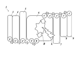
- FIG. 1 is an example of the configuration of the organic EL element 1 of the present invention, and is a schematic diagram corresponding to the configuration of (7) in the element configuration example.
- an organic functional layer having a hole injection layer 4, a hole transport layer 5, a light emitting layer 6, an electron transport layer 7 and an electron injection layer 8 between the anode 3 and the cathode 9 on the transparent substrate 2.
- F is provided.
- FIG. 2 is a schematic diagram showing a charge flow and light emission mechanism in the organic EL element.
- electrons (e ⁇ ) are injected from the cathode 9 into the electron injection layer 8
- holes (h + ) are injected from the anode 3 into the hole injection layer 4.
- the electrons and holes are respectively transported to the electron transport layer 7 and the hole transport layer 5 adjacent to the surface opposite to the electrode.
- an electron and a hole that are encountered in the light emitting layer 6 are recombined R to generate excitons, and a light emitting element using light (fluorescence / phosphorescence) L emitted when these return from the excited state to the ground state.
- It is an organic EL element.
- the organic functional layer extends from the hole injection layer to the electron injection layer.
- the first step is to inject charges from the electrode into the organic functional layer.
- Two injection mechanisms Schottky thermal radiation and tunnel injection, are known.
- the electric charge injected into the organic functional layer causes hopping conduction by using an external electric field applied between the two electrodes as a driving force. Will flow.
- the current at this time is a space charge limited current (SCLC) according to the child law instead of the Ohm law, and this is inversely proportional to the cube of the layer thickness as shown in the following equation (A).
- SCLC space charge limited current
- ⁇ voltage
- layer thickness 3
- a large current of several tens of A / m 2 needs to flow at a voltage of several volts, so that the layer thickness per layer is usually about 50 nm or less.
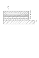
- FIG. 3 is a cross-sectional view showing an example of a solar cell having a single configuration (a configuration having one bulk heterojunction layer) composed of a bulk heterojunction organic photoelectric conversion element.
- a bulk heterojunction type organic photoelectric conversion element 10 has a transparent electrode (anode) 12, a hole transport layer 13, a photoelectric conversion unit 14 of a bulk heterojunction layer, an electron transport layer ( (Also referred to as a buffer layer) 15 and a counter electrode (cathode) 16 are sequentially stacked.
- the substrate 11 is a member that holds the transparent electrode 12, the photoelectric conversion unit 14, and the counter electrode 16 that are sequentially stacked. Since the photoelectrically converted light is incident from the substrate 11 side, the substrate 11 is a member that can transmit the photoelectrically converted light, that is, is transparent to the wavelength of the light to be photoelectrically converted. It is preferable.
- the substrate 11 for example, a glass substrate or a resin substrate is used.
- the photoelectric conversion unit 14 is a layer that converts light energy into electric energy, and includes a bulk heterojunction layer in which a p-type semiconductor material and an n-type semiconductor material are uniformly mixed.
- the p-type semiconductor material functions relatively as an electron donor (donor)
- the n-type semiconductor material functions relatively as an electron acceptor (acceptor).
- the electron donor and the electron acceptor are “an electron donor in which when electrons are absorbed, electrons move from the electron donor to the electron acceptor to form a hole-electron pair (charge separation state)”.
- an electron acceptor which does not simply donate or accept electrons like an electrode, but donates or accepts electrons by a photoreaction.
- FIG. 3 light incident from the transparent electrode 12 through the substrate 11 is absorbed by the electron acceptor or electron donor in the bulk heterojunction layer of the photoelectric conversion unit 14, and electrons move from the electron donor to the electron acceptor.
- a hole-electron pair charge separation state
- the generated charge is caused by an internal electric field, for example, when the work functions of the transparent electrode 12 and the counter electrode 16 are different, the electrons pass between the electron acceptors and the holes are electron donors due to the potential difference between the transparent electrode 12 and the counter electrode 16.
- the photocurrent is detected by passing through different electrodes. For example, when the work function of the transparent electrode 12 is larger than the work function of the counter electrode 16, electrons are transported to the transparent electrode 12 and holes are transported to the counter electrode 16.
- the organoborane complex of the present invention is a compound that easily conducts electrons because it can cope with various energy levels. Therefore, it can be applied as various materials for solar cells, particularly organic solar cells.
- Transistor> For the same reason as a solar cell, it can be suitably used as a transistor material.
- the organic borane complex of the present invention is a compound that easily causes electron hopping conduction. When a thin film is formed by itself, the organic borane complex basically becomes a thin film that conducts electrons.
- the organic borane complex of the present invention is conductive with a configuration such as laminating, coexisting with a metal such as silver, copper, nickel, iron, cobalt, or laminating the metal on the coexisting film. It can be applied to a reflective electrode, a transparent electrode, a semi-transmissive electrode, and the like.
- Organic borane-containing composition only needs to contain a borane complex, and may be in the form of a film or liquid.
- the organic functional layer in the organic EL element, the organic functional layer in the organic photoelectric conversion element, the organic functional layer in the transistor, the electrode / charge transfer thin film, the ink for inkjet, the toner for electrophotography, etc. Can be mentioned.
- the organic borane-containing composition of the present invention is used as an organic functional layer in an organic EL device, for example, it further contains a hole injection material, a hole transport material, a host material, a dopant material, an electron transport material, and an electron injection material. You may do it.
- the organic borane-containing composition of the present invention when used as an organic functional layer in an organic photoelectric conversion element, for example, it may further contain a p-type organic semiconductor, an n-type organic semiconductor, and a charge blocking material.
- the organic borane-containing composition of the present invention when used as an organic functional layer in a transistor, for example, it may further contain a p-type organic semiconductor and an n-type organic semiconductor.
- the organic borane-containing composition of the present invention is used as an electrode / charge-transfer thin film, it may further contain, for example, a metal or an alloy.
- the organic borane-containing composition of the present invention when used as an inkjet ink, for example, it may further contain a dye, an activator, and a solvent.
- the organic borane-containing composition of the present invention when used as an electrophotographic toner, for example, it may further contain a resin, a pigment, a wax, and a stabilizer.
- the organic borane complex of the present invention is used as it is without taking out the one produced in the system by the reaction of triarylborane with a substance capable of forming a coordination bond in the organic borane-containing composition exemplified above. May be.
- the most significant significance of the present invention is its durability, especially in the environment where an electronic device is exposed to exposure to an electronic device such as in air, at a high temperature, or when an electric field is applied.
- the borane complex was created. That is, compared with the conventional organic borane complex, by using the triarylborane having the structure represented by the general formula (1) or (2) according to the present invention, it is much more stable than the conventional organic borane complex. Can be improved.
- it is an organic borane complex that satisfies the requirements of the present invention the stability is universally improved and it can be applied to various industrial products. It can be said that this is an essential invention unlike any other.
- B3-PY of the present invention ⁇ Comparison of heat resistance ⁇ B3-PY of the present invention and the following triphenylborane pyridine complex were packed in different glass sealed tubes and heated to 300 ° C. B3-PY was taken out of the glass tube after heating at 300 ° C. for 1 hour, and 1 H-NMR was measured to confirm that it was not decomposed at all.
- the triphenylboranepyridine complex was measured for 1 H-NMR after heating at 300 ° C. for 1 hour. As a result, many new peaks different from the above triphenylboranepyridine complex appeared and decomposition occurred. It was confirmed. Further, when B3-DABCO-B3 of the present invention was subjected to a heat resistance test under the same conditions as described above, it was confirmed that it was not decomposed at all. From the above results, it was found that the compounds B3-PY and B3-DABCO-B3 of the present invention have sufficient thermal stability as compared with conventionally known triphenylborane pyridine complexes.
- An organic EL device was produced using the compound B3-PY of the present invention as an electron transport material.
- a glass substrate on which ITO (indium tin oxide) was deposited to a thickness of 100 nm as an anode was ultrasonically cleaned with isopropyl alcohol, dried with dry nitrogen gas and UV ozone cleaned, and fixed to a substrate holder of a vacuum deposition apparatus. After reducing the degree of vacuum in the vacuum deposition apparatus to 1 ⁇ 10 ⁇ 4 Pa, hexacyanohexaazatriphenylene (15 nm) as a hole injection layer and ⁇ -NPD (4,4′-) as a hole transport layer on the anode. Bis [N- (1-naphthyl) -N-phenylamino] biphenyl) (30 nm) was formed in this order.
- the compound B3-PY (15 nm) of the present invention was deposited as an electron transport layer, lithium fluoride (1.0 nm) as an electron injection layer, and aluminum (100 nm) as a cathode were vapor-deposited in this order to produce an organic EL device.
- a constant current of 2.5 mA / cm 2 was passed through the obtained organic EL device at room temperature, it emitted blue light. From this result, it was confirmed that B3-PY of the present invention functions as an electron transport material in an organic EL device, and it was found that B3-PY exhibits charge conductivity.
- An organic EL device was produced using the compound B3-PY of the present invention as a hole transport material.
- a glass substrate on which an ITO film having a thickness of 100 nm was formed as an anode was ultrasonically cleaned with isopropyl alcohol, dried with dry nitrogen gas and UV ozone cleaned, and fixed to a substrate holder of a vacuum deposition apparatus.
- hexacyanohexaazatriphenylene (12 nm) as a hole injection layer on the anode and the compound B3-DABCO-B3 of the present invention as a hole transport layer (40 nm) was formed in this order.
- 1,3-Bis (N-carbazolyl) benzene (mCP) as a host compound and Bis [2- (4,6-difluorophenyl) pyridinato-C2, N] (picolinato) iridium (III) as a light-emitting material are used.
- mCP N-carbazolyl
- Bis [2- (4,6-difluorophenyl) pyridinato-C2, N] (picolinato) iridium (III) as a light-emitting material.
- B3-PY of the present invention functions as a hole transport material in an organic EL device, and it was found that B3-PY exhibits charge conductivity.
- the organic borane complex of the present invention is applied to an organic functional layer such as a light emitting layer, a hole injection layer, a hole transport layer, an electron blocking layer, a hole blocking layer, an electron transport layer, an electron injection layer and an intermediate layer of an organic EL device.
- an organic functional layer such as a light emitting layer, a hole injection layer, a hole transport layer, an electron blocking layer, a hole blocking layer, an electron transport layer, an electron injection layer and an intermediate layer of an organic EL device.
- an organic borane-containing composition of the present invention includes an organic functional layer in an organic EL device, an organic functional layer in an organic photoelectric conversion device, an organic functional layer in a transistor, an electrode / charge-transfer thin film, an inkjet ink, an electronic It can be used for photographic toners.
Landscapes
- Chemical & Material Sciences (AREA)
- Engineering & Computer Science (AREA)
- Materials Engineering (AREA)
- Physics & Mathematics (AREA)
- Spectroscopy & Molecular Physics (AREA)
- Organic Chemistry (AREA)
- Inorganic Chemistry (AREA)
- Photovoltaic Devices (AREA)
- Electroluminescent Light Sources (AREA)
Abstract
本発明の課題は、ホウ素原子とアリール基上の炭素原子の結合が強化されたトリアリールボランを構成要素とする有機ボラン錯体を提供することである。 本発明の有機ボラン錯体は、下記一般式(1)で表される構造を有するトリアリールボランを構成要素として含むものである。 (式中、X1及びX2は、それぞれ独立に酸素原子又は硫黄原子を表す。X3及びX4は、それぞれ独立に水素原子又は置換基を表すが、X3とX4が1個の原子となって連結していてもよい。R1~R3は、それぞれ独立に水素原子又は置換基を表す。p、q及びrは、それぞれ独立に1~3の整数を表す。)
Description
本発明は、有機ボラン錯体、有機ボラン含有組成物及び有機エレクトロルミネッセンス素子に関する。より詳しくは、本発明は、ホウ素原子とアリール基上の炭素原子の結合が強化されたトリアリールボランを構成要素とする有機ボラン錯体等に関する。
ホウ素原子は、周期表では原子番号5、13族に属する3価の価数を持つ元素であり、原子状態での電子配置は、(1S)2、(2S)2、(2P)1となるが、2S軌道一つと2P軌道二つを使って、SP2混成軌道を形成することができる。
また、ホウ素原子は、この三つのSP2軌道に等価の電子がそれぞれ一つずつ(計三つ)配置されることで、炭素や酸素、窒素などの元素と共有結合を形成することが可能となり、あたかも3価の置換基のように取り扱うこともできる元素である。一方で、一つ余った空の2P軌道があることから、当然、ホウ素含有化合物は電子欠乏性を示すこととなる。
したがって、ホウ素原子と三つのアリールがホウ素-炭素結合を介して結合したトリアリールボラン系化合物は、基本的にこのホウ素原子の電子欠乏性的な性質により電子を受け入れやすく、非共有電子対を有する化合物や金属、すなわち、配位結合性の物質と相互作用や化学反応(以下、錯形成とも称する。)を起こしやすい。この時、ホウ素とアリール基との結合はSP3軌道となる。
また、ホウ素原子は、この三つのSP2軌道に等価の電子がそれぞれ一つずつ(計三つ)配置されることで、炭素や酸素、窒素などの元素と共有結合を形成することが可能となり、あたかも3価の置換基のように取り扱うこともできる元素である。一方で、一つ余った空の2P軌道があることから、当然、ホウ素含有化合物は電子欠乏性を示すこととなる。
したがって、ホウ素原子と三つのアリールがホウ素-炭素結合を介して結合したトリアリールボラン系化合物は、基本的にこのホウ素原子の電子欠乏性的な性質により電子を受け入れやすく、非共有電子対を有する化合物や金属、すなわち、配位結合性の物質と相互作用や化学反応(以下、錯形成とも称する。)を起こしやすい。この時、ホウ素とアリール基との結合はSP3軌道となる。
トリアリールボランと配位結合性の物質からなる有機ボラン錯体はいくつか知られている(例えば、特許文献1参照。)。しかしながら、有機ボラン錯体の構成要素(以下、ビルディングブロックともいう。)として用いるトリアリールボラン系化合物の安定性が低く、空気の不存在下、窒素等の不活性ガス中で取り扱うなど、その取り扱いに特殊な装置や技術が必要とされていた。よって、簡便な操作でより高い収率を上げられるよう更なる改良が求められていた。
また、トリアリールボランの安定性を向上させるために、トリアリールボランのホウ素原子の周りを、アルキル基やアリール基で立体的に嵩高くする方法が知られている(例えば、特許文献2参照。)。このような方法は、安定性は向上するが、トリアリールボラン系化合物と錯形成する配位結合性の物質の種類を広げるという観点からは改善の余地があった。
以上のように、従来の技術ではトリアリールボランを構成要素とする有機ボラン錯体の分子設計において、錯形成のしやすさと化合物の安定性がトレードオフの関係にあった。
また、トリアリールボランの安定性を向上させるために、トリアリールボランのホウ素原子の周りを、アルキル基やアリール基で立体的に嵩高くする方法が知られている(例えば、特許文献2参照。)。このような方法は、安定性は向上するが、トリアリールボラン系化合物と錯形成する配位結合性の物質の種類を広げるという観点からは改善の余地があった。
以上のように、従来の技術ではトリアリールボランを構成要素とする有機ボラン錯体の分子設計において、錯形成のしやすさと化合物の安定性がトレードオフの関係にあった。
本発明は、上記問題・状況に鑑みてなされたものであり、その解決課題は、ホウ素原子とアリール基上の炭素原子の結合が強化されたトリアリールボランを構成要素とする有機ボラン錯体、有機ボラン含有組成物及び有機エレクトロルミネッセンス素子を提供することである。
本発明者は、上記課題を解決すべく上記問題の原因等について検討し、トリアリールボランの安定性を向上させるために、ホウ素原子が三つのアリール基とホウ素-炭素結合を介して結合したトリアリールボランであって、該化合物中の前記三つのアリール基が、ホウ素原子を中心に電子供与性の2価の原子を介してそれぞれ隣り合うアリール基同士の少なくとも二つの組み合わせにおける分子設計に注目した。
その結果、立体障害が小さく、電子供与性の2価の原子で架橋されたトリアリールボランを構成要素とすることで、非共有電子対を有する化合物や金属又は金属化合物等との配位結合を形成し得る物質との有機ボラン錯体の安定性が向上することを見いだし、本発明に至った。
すなわち、本発明の上記課題は、下記の手段により解決される。
その結果、立体障害が小さく、電子供与性の2価の原子で架橋されたトリアリールボランを構成要素とすることで、非共有電子対を有する化合物や金属又は金属化合物等との配位結合を形成し得る物質との有機ボラン錯体の安定性が向上することを見いだし、本発明に至った。
すなわち、本発明の上記課題は、下記の手段により解決される。
1.下記一般式(1)で表される構造を有するトリアリールボランを構成要素として含む有機ボラン錯体。

(式中、X1及びX2は、それぞれ独立に酸素原子又は硫黄原子を表す。X3及びX4は、それぞれ独立に水素原子又は置換基を表すが、X3とX4が1個の原子となって連結していてもよい。R1~R3は、それぞれ独立に水素原子又は置換基を表す。p、q及びrは、それぞれ独立に1~3の整数を表す。)
2.前記一般式(1)において、X3とX4が1個の原子となって連結しており、
該原子が、酸素原子又は硫黄原子である第1項に記載の有機ボラン錯体。
該原子が、酸素原子又は硫黄原子である第1項に記載の有機ボラン錯体。
3.前記一般式(1)で表される構造を有するトリアリールボランと、非共有電子対を有する化合物、金属又は金属化合物とを、構成成分として含む第1項又は第2項に記載の有機ボラン錯体。
4.前記一般式(1)で表される構造を有するトリアリールボランが、下記一般式(2)で表される構造を有するトリアリールボランである第1項から第3項までのいずれか一項に記載の有機ボラン錯体。

(式中、R1~R3は、それぞれ独立に水素原子又は置換基を表す。p、q及びrは、それぞれ独立に1~3の整数を表す。)
5.第1項から第4項までのいずれか一項に記載の有機ボラン錯体を含有する有機ボラン含有組成物。
6.第1項から第4項までのいずれか一項に記載の有機ボラン錯体を含有する有機機能層を有する有機エレクトロルミネッセンス素子。
本発明の上記手段により、ホウ素原子とアリール基上の炭素原子の結合が強化されたトリアリールボランを構成要素とする有機ボラン錯体、有機ボラン含有組成物及び有機エレクトロルミネッセンス素子を提供することができる。
本発明の効果の発現機構又は作用機構については、明確にはなっていないが、以下のように考えている。本発明の有機ボラン錯体は、立体障害が小さく、電子供与性の2価の原子によって任意のアリール基が架橋されることで、該化合物と非共有電子対を有する化合物や金属と配位結合の形成しやすさと、生成した有機ボラン錯体の安定性を両立できたものと考えられる。
これらの特性は、トリアリールボランにおいて、アリール基の架橋基として酸素原子又は硫黄原子がホウ素原子周辺に存在することが重要だと考えている。すなわち、該トリアリールボランと非共有電子対を有する化合物や金属との有機ボラン錯体の合成にあたって、非共有電子対を有する化合物や金属が該トリアリールボランと反応する際に、大きな立体障害がなく容易に接近して配位結合を形成できるものと考えている。更には、ホウ素原子と三つのアリール基のホウ素-炭素結合が強化され、該有機ボラン錯体が熱、水分、又は酸素による分解を受けにくくなったためであると推察している。
これらの特性は、トリアリールボランにおいて、アリール基の架橋基として酸素原子又は硫黄原子がホウ素原子周辺に存在することが重要だと考えている。すなわち、該トリアリールボランと非共有電子対を有する化合物や金属との有機ボラン錯体の合成にあたって、非共有電子対を有する化合物や金属が該トリアリールボランと反応する際に、大きな立体障害がなく容易に接近して配位結合を形成できるものと考えている。更には、ホウ素原子と三つのアリール基のホウ素-炭素結合が強化され、該有機ボラン錯体が熱、水分、又は酸素による分解を受けにくくなったためであると推察している。
本発明の有機ボラン錯体は、前記一般式(1)で表される構造を有するトリアリールボランを構成要素として含むことを特徴とする。
この特徴は、下記実施態様に係る発明に共通する又は対応する技術的特徴である。
この特徴は、下記実施態様に係る発明に共通する又は対応する技術的特徴である。
また、前記一般式(1)において、本発明の効果発現の観点から、X3とX4が1個の原子となって連結しており、該原子が、酸素原子又は硫黄原子であることが好ましい。
また、前記一般式(1)で表される構造を有するトリアリールボランと、非共有電子対を有する化合物、金属又は金属化合物とを、構成成分として含むことが、錯体形成の観点から好ましい。
また、前記一般式(1)で表される構造を有するトリアリールボランが、前記一般式(2)で表される構造を有するトリアリールボランであることが、錯体の安定性向上の観点から好ましい。
また、本発明の有機ボラン含有組成物は、本発明の有機ボラン錯体を含有することが、当該組成物の安定性向上の観点から好ましい。
また、本発明の有機エレクトロルミネッセンス素子は、本発明の有機ボラン錯体を含有する有機機能層を有することが、当該素子性能の向上の観点から好ましい。
以下、本発明とその構成要素及び本発明を実施するための形態・態様について詳細な説明をする。なお、以下の説明において示す「~」は、その前後に記載される数値を下限値及び上限値として含む意味で使用する。
《有機ボラン錯体の分子設計》
本発明の有機ボラン錯体は、三つのアリール基とホウ素原子がホウ素-炭素結合を介して結合したトリアリールボランを構成要素(ビルディングブロック)としている。
このトリアリールボラン中の前記三つのアリール基のそれぞれ隣り合うアリール基同士の少なくとも二つの組み合わせは、立体障害が小さく、かつ電子供与性の2価の原子で架橋されている。さらに、このトリアリールボランが有機ボラン錯体を形成するにあたり、ホウ素原子の空の2P軌道に対して、非共有電子対を有する化合物や金属から電子が供給されることで、配位結合を形成する。なお、ここでいう配位結合とは、結合を形成する二つの原子の一方からのみ結合電子が分子軌道に提供される化学結合であることを意味する。
そこで、本発明に係る一般式(1)で表される構造を有するトリアリールボランの、ホウ素原子の空の2P軌道に対して電子を供給できる物質を原料として用いた有機ボラン錯体は、本質的に本発明と同じ技術思想に則った化合物であるため、本発明の化合物と一義的に決めることができる。
本発明の有機ボラン錯体は、三つのアリール基とホウ素原子がホウ素-炭素結合を介して結合したトリアリールボランを構成要素(ビルディングブロック)としている。
このトリアリールボラン中の前記三つのアリール基のそれぞれ隣り合うアリール基同士の少なくとも二つの組み合わせは、立体障害が小さく、かつ電子供与性の2価の原子で架橋されている。さらに、このトリアリールボランが有機ボラン錯体を形成するにあたり、ホウ素原子の空の2P軌道に対して、非共有電子対を有する化合物や金属から電子が供給されることで、配位結合を形成する。なお、ここでいう配位結合とは、結合を形成する二つの原子の一方からのみ結合電子が分子軌道に提供される化学結合であることを意味する。
そこで、本発明に係る一般式(1)で表される構造を有するトリアリールボランの、ホウ素原子の空の2P軌道に対して電子を供給できる物質を原料として用いた有機ボラン錯体は、本質的に本発明と同じ技術思想に則った化合物であるため、本発明の化合物と一義的に決めることができる。
《トリアリールボラン》
以下に、本発明に係る下記一般式(1)で表される構造を有するトリアリールボランについて説明する。
以下に、本発明に係る下記一般式(1)で表される構造を有するトリアリールボランについて説明する。

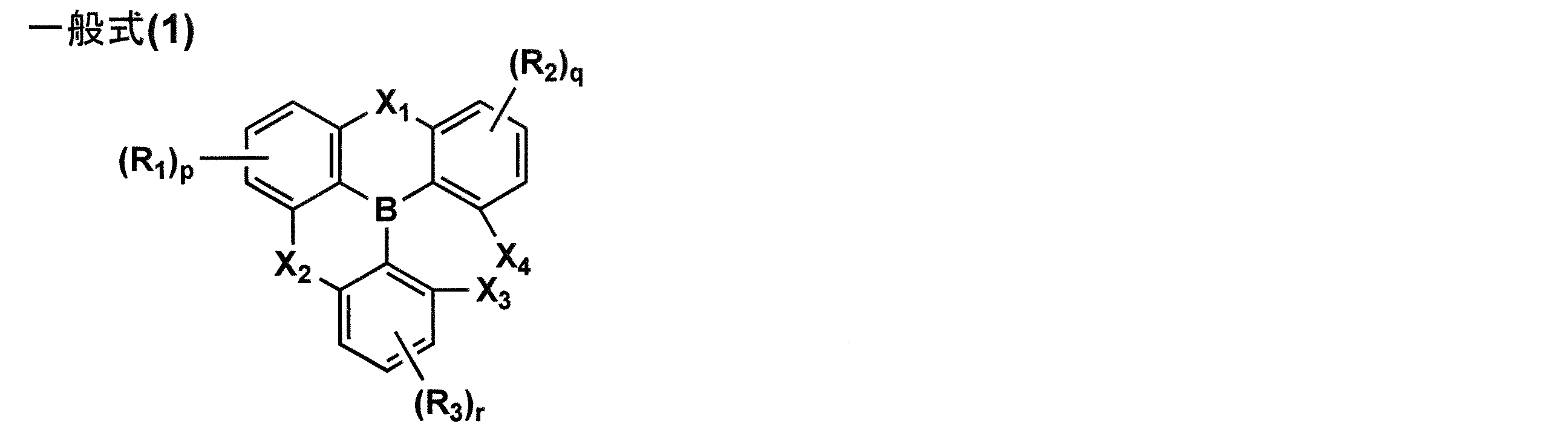
式中、X1及びX2は、それぞれ独立に酸素原子又は硫黄原子を表す。X3及びX4は、それぞれ独立に水素原子又は置換基を表すが、X3とX4が1個の原子となって連結していてもよい。R1~R3は、それぞれ独立に水素原子又は置換基を表す。p、q及びrは、それぞれ独立に1~3の整数を表す。
X3及びX4が表す置換基としては、例えば、鎖状アルキル基、環状アルキル基、アルコキシ基、アリールオキシ基、エステル基、スルホン酸エステル基、ハロゲン原子、シアノ基、ヒドロキシ基、芳香族炭化水素環基、又は芳香族複素環基を挙げることができる。
鎖状アルキル基としては、直鎖でも分岐していても良い。例えば直鎖状アルキル基としては、メチル基、エチル基、プロピル基、ブチル基、ペンチル基又はヘキシル基等が挙げられる。
分枝状アルキル基としては、イソプロピル基、イソブチル基、sec-ブチル基、tert-ブチル基、シクロプロピルメチル基、シクロプロピルエチル基、シクロブチルメチル基、シクロブチルエチル基、シクロペンチルメチル基、シクロペンチルエチル基、シクロヘキシルメチル基、又はシクロヘキシルエチル基などを挙げることができる。
環状アルキル基としては、シクロプロピル基、シクロブチル基、シクロペンチル基、シクロヘキシル基又はシクロヘプチル基等を挙げることができる。
芳香族炭化水素環基としては、フェニル基、p-クロロフェニル基、メシチル基、トリル基、キシリル基、ナフチル基、アントリル基、アズレニル基、アセナフテニル基、フルオレニル基、フェナントリル基、インデニル基、ピレニル基、ビフェニリル基等を挙げることができる。
アルコキシ基としては、メトキシ基、エトキシ基、n-プロポキシ基、イソプロポキシ基、n-ブトキシ基等を挙げることができる。
アリールオキシ基としては、フェノキシ基、ナフトキシ基等を挙げることができる。
エステル基としては、アセトキシ基、ベンゾイルオキシ基等を挙げることができる。
スルホン酸エステル基としては、メタンスルホン酸エステル基、トリフルオロメタンスルホン酸エステル基、ベンゼンスルホン酸エステル基等を挙げることができる。
ハロゲン原子としては、フッ素原子、塩素原子、臭素原子等を挙げることができる。
芳香族複素環基としては、ピリジル基、ピリミジニル基、フリル基、ピロリル基、イミダゾリル基、ベンゾイミダゾリル基、ピラゾリル基、ピラジニル基、トリアゾリル基(例えば、1,2,4-トリアゾール-1-イル基、1,2,3-トリアゾール-1-イル基等)、オキサゾリル基、ベンゾオキサゾリル基、チアゾリル基、イソオキサゾリル基、イソチアゾリル基、フラザニル基、チエニル基、キノリル基、ベンゾフリル基、ジベンゾフリル基、ベンゾチエニル基、ジベンゾチエニル基、インドリル基、カルバゾリル基、カルボリニル基、ジアザカルバゾリル基(前記カルボリニル基のカルボリン環を構成する炭素原子の一つが窒素原子で置き換わったものを示す。)、キノキサリニル基、ピリダジニル基、トリアジニル基、キナゾリニル基、フタラジニル基等を挙げることができる。
これらの置換基は、任意の位置にさらに置換基を有していても良く、例えば、フェニル基、ピリジル基、ピロール基、チエニル基、フリル基、イミダゾリル基、ピリミジル基、ピラジル基、ピリダジル基、トリアジニル基などの芳香族基、及びそれらがさらに縮合した縮合芳香族基(例えば、ナフチル基、キノリル基、イミダゾリル基、インドロイミダゾリル基、イミダゾイミダゾリル基、ジベンゾチエニル基、ジベンゾフリル基、アザジベンゾフリル基、ベンズイミダゾリル基、キナゾリル基、ベンゾピラジニル基、など)、アルキル、分岐アルキル、シクロアルキル、アルケニル、アルキニル等の脂肪族基、シアノ基、アルコキシ基、アリールオキシ基、アルキルチオ基、アリールチオ基、アミノ基、カルボニル基、アシル基、エステル基、ウレイド基、ウレタン基、などの置換基、フッ素原子、塩素原子等のハロゲン原子等が挙げられる。
X3及びX4が表す置換基としては、例えば、鎖状アルキル基、環状アルキル基、アルコキシ基、アリールオキシ基、エステル基、スルホン酸エステル基、ハロゲン原子、シアノ基、ヒドロキシ基、芳香族炭化水素環基、又は芳香族複素環基を挙げることができる。
鎖状アルキル基としては、直鎖でも分岐していても良い。例えば直鎖状アルキル基としては、メチル基、エチル基、プロピル基、ブチル基、ペンチル基又はヘキシル基等が挙げられる。
分枝状アルキル基としては、イソプロピル基、イソブチル基、sec-ブチル基、tert-ブチル基、シクロプロピルメチル基、シクロプロピルエチル基、シクロブチルメチル基、シクロブチルエチル基、シクロペンチルメチル基、シクロペンチルエチル基、シクロヘキシルメチル基、又はシクロヘキシルエチル基などを挙げることができる。
環状アルキル基としては、シクロプロピル基、シクロブチル基、シクロペンチル基、シクロヘキシル基又はシクロヘプチル基等を挙げることができる。
芳香族炭化水素環基としては、フェニル基、p-クロロフェニル基、メシチル基、トリル基、キシリル基、ナフチル基、アントリル基、アズレニル基、アセナフテニル基、フルオレニル基、フェナントリル基、インデニル基、ピレニル基、ビフェニリル基等を挙げることができる。
アルコキシ基としては、メトキシ基、エトキシ基、n-プロポキシ基、イソプロポキシ基、n-ブトキシ基等を挙げることができる。
アリールオキシ基としては、フェノキシ基、ナフトキシ基等を挙げることができる。
エステル基としては、アセトキシ基、ベンゾイルオキシ基等を挙げることができる。
スルホン酸エステル基としては、メタンスルホン酸エステル基、トリフルオロメタンスルホン酸エステル基、ベンゼンスルホン酸エステル基等を挙げることができる。
ハロゲン原子としては、フッ素原子、塩素原子、臭素原子等を挙げることができる。
芳香族複素環基としては、ピリジル基、ピリミジニル基、フリル基、ピロリル基、イミダゾリル基、ベンゾイミダゾリル基、ピラゾリル基、ピラジニル基、トリアゾリル基(例えば、1,2,4-トリアゾール-1-イル基、1,2,3-トリアゾール-1-イル基等)、オキサゾリル基、ベンゾオキサゾリル基、チアゾリル基、イソオキサゾリル基、イソチアゾリル基、フラザニル基、チエニル基、キノリル基、ベンゾフリル基、ジベンゾフリル基、ベンゾチエニル基、ジベンゾチエニル基、インドリル基、カルバゾリル基、カルボリニル基、ジアザカルバゾリル基(前記カルボリニル基のカルボリン環を構成する炭素原子の一つが窒素原子で置き換わったものを示す。)、キノキサリニル基、ピリダジニル基、トリアジニル基、キナゾリニル基、フタラジニル基等を挙げることができる。
これらの置換基は、任意の位置にさらに置換基を有していても良く、例えば、フェニル基、ピリジル基、ピロール基、チエニル基、フリル基、イミダゾリル基、ピリミジル基、ピラジル基、ピリダジル基、トリアジニル基などの芳香族基、及びそれらがさらに縮合した縮合芳香族基(例えば、ナフチル基、キノリル基、イミダゾリル基、インドロイミダゾリル基、イミダゾイミダゾリル基、ジベンゾチエニル基、ジベンゾフリル基、アザジベンゾフリル基、ベンズイミダゾリル基、キナゾリル基、ベンゾピラジニル基、など)、アルキル、分岐アルキル、シクロアルキル、アルケニル、アルキニル等の脂肪族基、シアノ基、アルコキシ基、アリールオキシ基、アルキルチオ基、アリールチオ基、アミノ基、カルボニル基、アシル基、エステル基、ウレイド基、ウレタン基、などの置換基、フッ素原子、塩素原子等のハロゲン原子等が挙げられる。
前記一般式(1)において、X3及びX4が1個の原子となって連結していてもよく、X3とX4が1個の原子となって連結する場合、該原子は酸素原子、又は硫黄原子であることが好ましい。
前記一般式(1)において、R1~R3は、それぞれ独立に水素原子又は置換基を表し、該置換基としては、前記X3及びX4で説明した置換基と同様の基を挙げることができる。
前記一般式(1)において、p、q及びrは、それぞれ独立に1~3の整数を表す。p、q及びrが2又は3の場合、複数のR1~R3は、各々同じであっても異なっていてもよい。
前記一般式(1)において、R1~R3は、それぞれ独立に水素原子又は置換基を表し、該置換基としては、前記X3及びX4で説明した置換基と同様の基を挙げることができる。
前記一般式(1)において、p、q及びrは、それぞれ独立に1~3の整数を表す。p、q及びrが2又は3の場合、複数のR1~R3は、各々同じであっても異なっていてもよい。
本発明の実施態様としては、前記一般式(1)で表される構造を有するトリアリールボランが、下記一般式(2)で表される構造を有するトリアリールボランであることが好ましい。
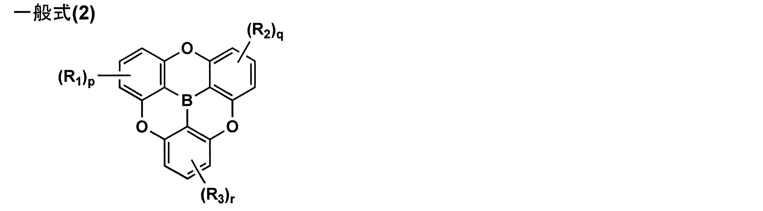
式中、R1~R3は、それぞれ独立に水素原子又は置換基を表す。p、q及びrは、それぞれ独立に1~3の整数を表す。
R1~R3が表す置換基としては、例えば、前記一般式(1)におけるR1~R3が表す置換基と同様の基を挙げることができる。これらの置換基は、任意の位置にさらに置換基を有していても良い。
p、q及びrが2又は3の場合、複数のR1~R3は各々同じであっても異なっていてもよい。
R1~R3が表す置換基としては、例えば、前記一般式(1)におけるR1~R3が表す置換基と同様の基を挙げることができる。これらの置換基は、任意の位置にさらに置換基を有していても良い。
p、q及びrが2又は3の場合、複数のR1~R3は各々同じであっても異なっていてもよい。
〈トリアリールボランの具体例〉
以下に、本発明に係る前記一般式(1)又は一般式(2)で表される構造を有するトリアリールボランの一例を示す。
以下に、本発明に係る前記一般式(1)又は一般式(2)で表される構造を有するトリアリールボランの一例を示す。

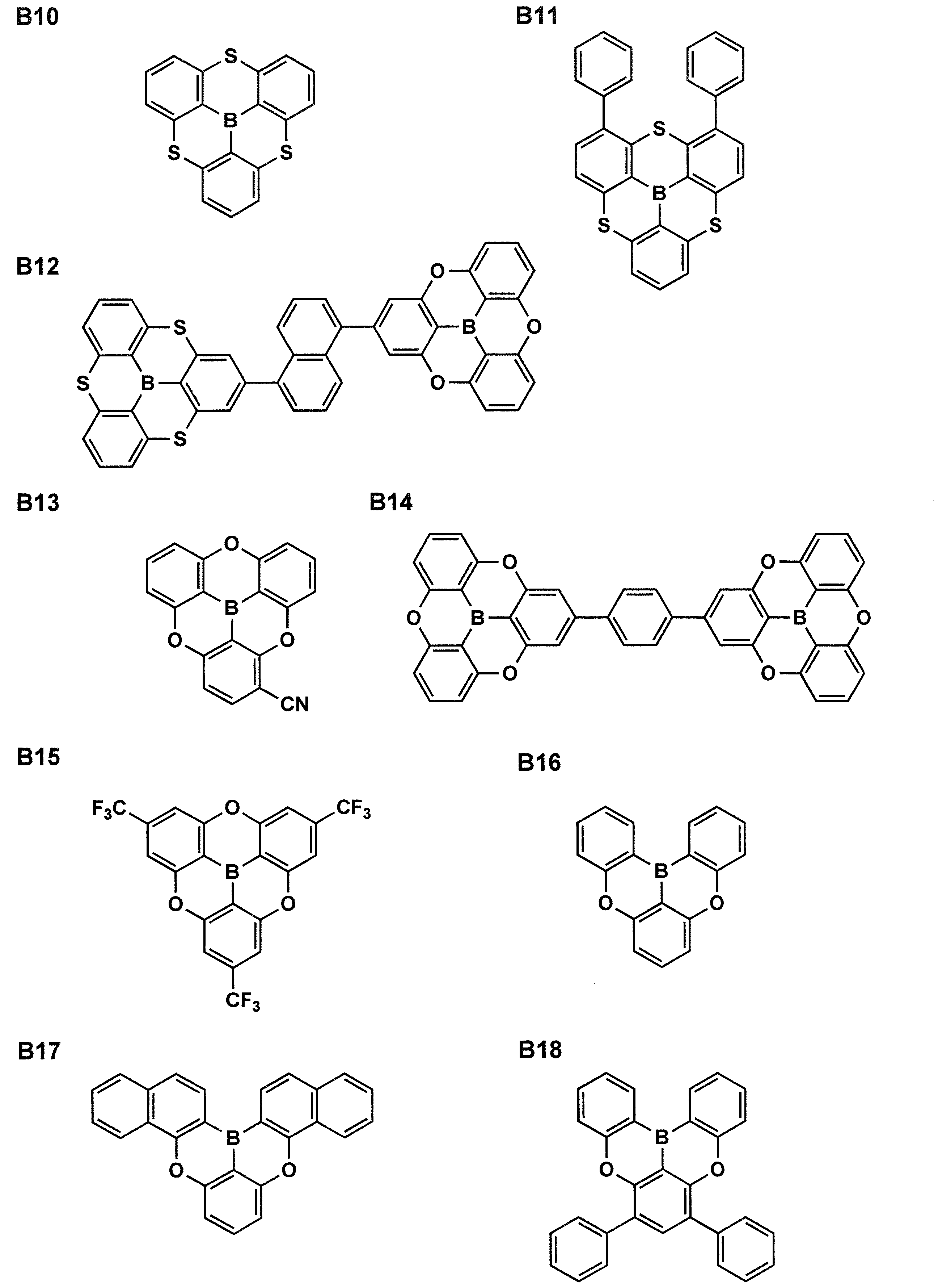
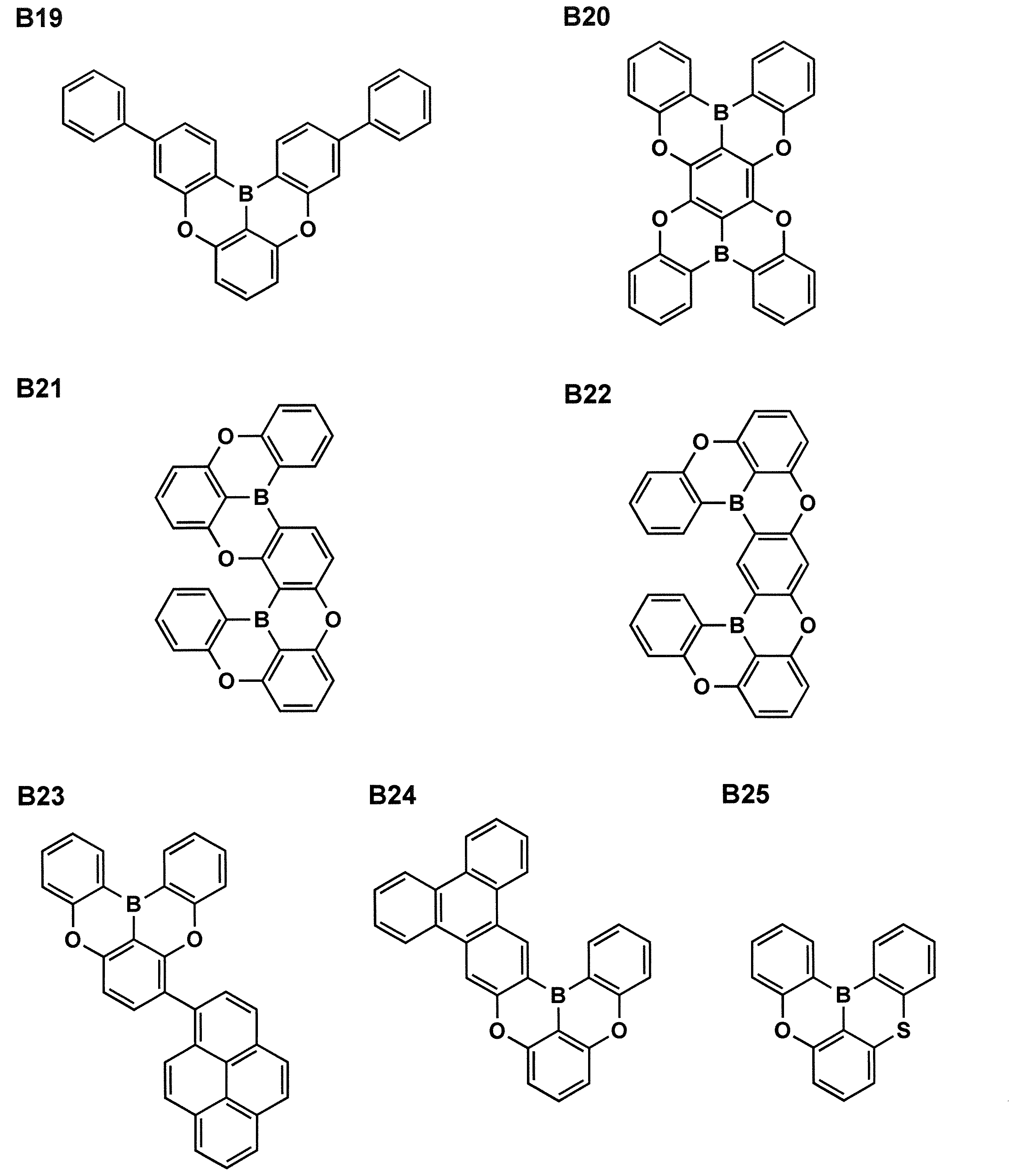
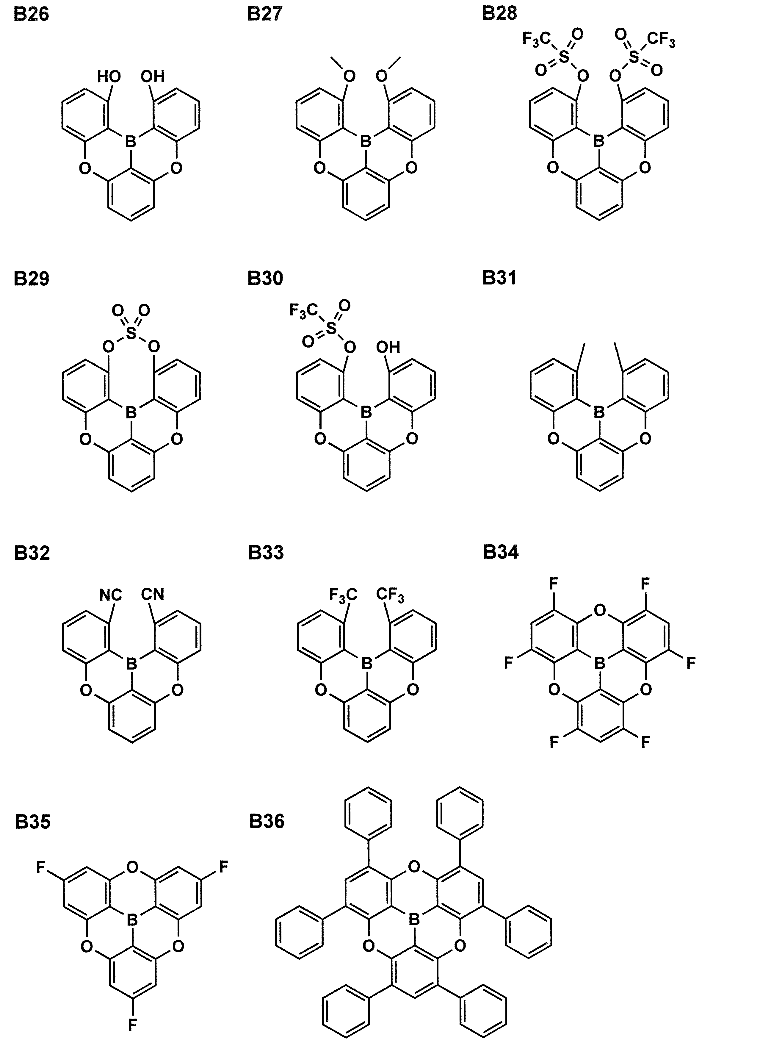
《有機ボラン錯体》
前記一般式(1)又は一般式(2)で表される構造を有するトリアリールボランをビルディングブロックとする有機ボラン錯体について説明する。
ビルディングブロックとは、本発明の有機ボラン錯体の構成要素であることを意味する。
トリアリールボランをビルディングブロックとした有機ボラン錯体とは、一般式(1)で表される構造を有するトリアリールボランと、配位結合を形成し得る物質との反応により形成された錯体を意味する。
配位結合を形成し得る物質(X)とは、非共有電子対を有する化合物や金属又は金属化合物であることが好ましい。具体的には、アミン類(例えば、トリメチルアミン等のトリアルキルアミン類、ジエチルアミン等のジアルキルアミン類、ジメチルフェニルアミン等のアリールジアルキルアミン等、トリフェニルアミン等のトリアリールアミン類、ピペリジン、ピペラジン等の環状アミン類等)、芳香族複素環化合物(例えば、ピリジン、ピリミジン、アザカルバゾール、アザジベンゾフラン、イミダゾール、ピラゾール、ピロール、トリアゾール、オキサジアゾール、オキサゾール、イソオキサゾール、チアゾール、チアジアゾール等)、オキシド類(例えば、ホスフィンオキシド、ピリジンやトリアルキルアミンのN-オキシド、スルホキシド等)、典型金属原子、遷移金属原子、及びそのイオン、ハロゲンイオン(フッ素イオン、塩素イオン等)、4配位平面錯体(例えば、プラチナオルトメタル錯体、ニッケル錯体、亜鉛錯体等)等を挙げることができる。
すなわち、本発明の有機ボラン錯体は、前記一般式(1)で表される構造を有するトリアリールボランと、非共有電子対を有する化合物、金属又は金属化合物とを、構成成分として含むことが好ましい。
前記一般式(1)又は一般式(2)で表される構造を有するトリアリールボランをビルディングブロックとする有機ボラン錯体について説明する。
ビルディングブロックとは、本発明の有機ボラン錯体の構成要素であることを意味する。
トリアリールボランをビルディングブロックとした有機ボラン錯体とは、一般式(1)で表される構造を有するトリアリールボランと、配位結合を形成し得る物質との反応により形成された錯体を意味する。
配位結合を形成し得る物質(X)とは、非共有電子対を有する化合物や金属又は金属化合物であることが好ましい。具体的には、アミン類(例えば、トリメチルアミン等のトリアルキルアミン類、ジエチルアミン等のジアルキルアミン類、ジメチルフェニルアミン等のアリールジアルキルアミン等、トリフェニルアミン等のトリアリールアミン類、ピペリジン、ピペラジン等の環状アミン類等)、芳香族複素環化合物(例えば、ピリジン、ピリミジン、アザカルバゾール、アザジベンゾフラン、イミダゾール、ピラゾール、ピロール、トリアゾール、オキサジアゾール、オキサゾール、イソオキサゾール、チアゾール、チアジアゾール等)、オキシド類(例えば、ホスフィンオキシド、ピリジンやトリアルキルアミンのN-オキシド、スルホキシド等)、典型金属原子、遷移金属原子、及びそのイオン、ハロゲンイオン(フッ素イオン、塩素イオン等)、4配位平面錯体(例えば、プラチナオルトメタル錯体、ニッケル錯体、亜鉛錯体等)等を挙げることができる。
すなわち、本発明の有機ボラン錯体は、前記一般式(1)で表される構造を有するトリアリールボランと、非共有電子対を有する化合物、金属又は金属化合物とを、構成成分として含むことが好ましい。
トリアリールボランの分子内にホウ素原子が複数ある場合、又は/及び配位結合を形成し得る物質の分子内に配位性の原子が複数ある場合、それらが反応して超分子様に連なった化合物であってもよい。
さらに、本発明の有機ボラン錯体が第三の成分と相互作用した化合物も本発明に含めることができる。例えば、本発明の有機ボラン錯体から成るアート錯体と金属陽イオン(例えば、ナトリウムイオン、カリウムイオン)との塩、本発明の有機ボラン錯体がフラーレン(例えば、C60、C70等)を包摂した化合物、及び該包摂体が超分子様に連なった化合物を挙げることができる。
さらに、本発明の有機ボラン錯体が第三の成分と相互作用した化合物も本発明に含めることができる。例えば、本発明の有機ボラン錯体から成るアート錯体と金属陽イオン(例えば、ナトリウムイオン、カリウムイオン)との塩、本発明の有機ボラン錯体がフラーレン(例えば、C60、C70等)を包摂した化合物、及び該包摂体が超分子様に連なった化合物を挙げることができる。
〈有機ボラン錯体の代表例〉
本発明に係るトリアリールボランとして前記例示化合物B3を用いて、有機ボラン錯体を説明する。
本発明に係るトリアリールボランは、ホウ素原子はSP2軌道を介する結合で3個のアリール基と結合すると当時に、ホウ素原子上に空の2P軌道を有する。したがって、下記のように、例示化合物B3は円盤状の構造となる。
本発明に係るトリアリールボランとして前記例示化合物B3を用いて、有機ボラン錯体を説明する。
本発明に係るトリアリールボランは、ホウ素原子はSP2軌道を介する結合で3個のアリール基と結合すると当時に、ホウ素原子上に空の2P軌道を有する。したがって、下記のように、例示化合物B3は円盤状の構造となる。

次に、このようなトリアリールボランが配位結合を形成し得る物質(X)と反応すると、ホウ素原子からの結合はSP3軌道を介するものとなり、例示化合物B3をビルディングブロックとする有機ボラン錯体は、下記のように、撓んだ、お椀型の構造となる。

以下、本発明の有機ボラン錯体の代表例を模式的に示すが、本発明はこれらに限定されない。

《有機ボラン錯体の合成》
本発明の有機ボラン錯体の合成において用いられる溶媒としては、アルコール系、エステル系、エーテル系、ケトン系、ハロゲン系、ニトリル系、アミド系、芳香族炭化水素系等の各種溶媒、及びそれらを組み合わせた溶媒を併せて用いることができる。具体的には、メタノール、エタノール、イソプロパノール、酢酸エチル、テトラヒドロフラン、アセトン、ジクロロメタン、アセトニトリル、N,N-ジメチルホルムアミド、N,N-ジメチルアセトアミド及びトルエン等を挙げることができる。
用いる溶媒の量は、特に限定されないが、原料に対し重量で200倍までの範囲で用いることが好ましく、5~50倍の範囲で用いることがより好ましい。
本発明においては、反応温度は0~120℃の範囲内であるのが好ましく、室温付近(15~30℃)であることがより好ましい。
本発明の有機ボラン錯体の合成において、トリアリールボランのホウ素原子に換算したモル数に対して、0.9~1.2モル当量の範囲内の配位結合を形成し得る物質を用いることが好ましく、1.0~1.1モル当量の範囲内の配位結合を形成し得る物質を用いることがより好ましい。
本発明の有機ボラン錯体の合成において用いられる溶媒としては、アルコール系、エステル系、エーテル系、ケトン系、ハロゲン系、ニトリル系、アミド系、芳香族炭化水素系等の各種溶媒、及びそれらを組み合わせた溶媒を併せて用いることができる。具体的には、メタノール、エタノール、イソプロパノール、酢酸エチル、テトラヒドロフラン、アセトン、ジクロロメタン、アセトニトリル、N,N-ジメチルホルムアミド、N,N-ジメチルアセトアミド及びトルエン等を挙げることができる。
用いる溶媒の量は、特に限定されないが、原料に対し重量で200倍までの範囲で用いることが好ましく、5~50倍の範囲で用いることがより好ましい。
本発明においては、反応温度は0~120℃の範囲内であるのが好ましく、室温付近(15~30℃)であることがより好ましい。
本発明の有機ボラン錯体の合成において、トリアリールボランのホウ素原子に換算したモル数に対して、0.9~1.2モル当量の範囲内の配位結合を形成し得る物質を用いることが好ましく、1.0~1.1モル当量の範囲内の配位結合を形成し得る物質を用いることがより好ましい。
《有機ボラン錯体の電子デバイスへの応用》
本発明の有機ボラン錯体は、トリアリールボランと配位結合を形成し得る物質を適宜選択することにより、バイポーラー性を有する錯体にすることも可能である。
また、様々なエネルギー準位に対応できることから、発光性(ゲスト)材料、ホスト材料として使用できるのみならず、正孔輸送材料、正孔注入材料、電子輸送材料、電子注入材料としても使用することができる。
すなわち、本発明の有機ボラン錯体は、有機EL素子の発光層、正孔注入層、正孔輸送層、電子阻止層、正孔阻止層、電子輸送層、電子注入層及び中間層等の有機機能層に用いることができる。さらには、有機EL素子のみならず様々な電子デバイスに用いることができる。
本発明の有機ボラン錯体は、トリアリールボランと配位結合を形成し得る物質を適宜選択することにより、バイポーラー性を有する錯体にすることも可能である。
また、様々なエネルギー準位に対応できることから、発光性(ゲスト)材料、ホスト材料として使用できるのみならず、正孔輸送材料、正孔注入材料、電子輸送材料、電子注入材料としても使用することができる。
すなわち、本発明の有機ボラン錯体は、有機EL素子の発光層、正孔注入層、正孔輸送層、電子阻止層、正孔阻止層、電子輸送層、電子注入層及び中間層等の有機機能層に用いることができる。さらには、有機EL素子のみならず様々な電子デバイスに用いることができる。
《有機エレクトロルミネッセンス素子》
本発明の有機エレクトロルミネッセンス素子(以下、有機EL素子ともいう。)は、陽極と陰極の間に少なくとも発光層を含む有機機能層を有する有機EL素子であって、有機機能層の少なくとも1層が、本発明の有機ボラン錯体を含有するものである。
本発明の有機ボラン錯体を含有する有機EL素子は、照明装置及び表示装置に好適に具備され得る。
本発明の有機ボラン錯体を含有する有機EL素子における代表的な素子構成としては、以下の構成を挙げることができるが、これらに限定されるものではない。
(1)陽極/発光層/陰極
(2)陽極/発光層/電子輸送層/陰極
(3)陽極/正孔輸送層/発光層/陰極
(4)陽極/正孔輸送層/発光層/電子輸送層/陰極
(5)陽極/正孔輸送層/発光層/電子輸送層/電子注入層/陰極
(6)陽極/正孔注入層/正孔輸送層/発光層/電子輸送層/陰極
(7)陽極/正孔注入層/正孔輸送層/(電子阻止層/)発光層/(正孔阻止層/)電子輸送層/電子注入層/陰極
上記の中で(7)の構成が好ましく用いられるが、これに限定されるものではない。
発光層は、単層又は複数層で構成されており、発光層が複数の場合は各発光層の間に非発光性の中間層を設けてもよい。
必要に応じて、発光層と陰極との間に正孔阻止層(正孔障壁層ともいう。)や電子注入層(陰極バッファー層ともいう。)を設けてもよく、また、発光層と陽極との間に電子阻止層(電子障壁層ともいう)や正孔注入層(陽極バッファー層ともいう。)を設けてもよい。
本発明の有機エレクトロルミネッセンス素子(以下、有機EL素子ともいう。)は、陽極と陰極の間に少なくとも発光層を含む有機機能層を有する有機EL素子であって、有機機能層の少なくとも1層が、本発明の有機ボラン錯体を含有するものである。
本発明の有機ボラン錯体を含有する有機EL素子は、照明装置及び表示装置に好適に具備され得る。
本発明の有機ボラン錯体を含有する有機EL素子における代表的な素子構成としては、以下の構成を挙げることができるが、これらに限定されるものではない。
(1)陽極/発光層/陰極
(2)陽極/発光層/電子輸送層/陰極
(3)陽極/正孔輸送層/発光層/陰極
(4)陽極/正孔輸送層/発光層/電子輸送層/陰極
(5)陽極/正孔輸送層/発光層/電子輸送層/電子注入層/陰極
(6)陽極/正孔注入層/正孔輸送層/発光層/電子輸送層/陰極
(7)陽極/正孔注入層/正孔輸送層/(電子阻止層/)発光層/(正孔阻止層/)電子輸送層/電子注入層/陰極
上記の中で(7)の構成が好ましく用いられるが、これに限定されるものではない。
発光層は、単層又は複数層で構成されており、発光層が複数の場合は各発光層の間に非発光性の中間層を設けてもよい。
必要に応じて、発光層と陰極との間に正孔阻止層(正孔障壁層ともいう。)や電子注入層(陰極バッファー層ともいう。)を設けてもよく、また、発光層と陽極との間に電子阻止層(電子障壁層ともいう)や正孔注入層(陽極バッファー層ともいう。)を設けてもよい。
電子輸送層とは、電子を輸送する機能を有する層であり、広い意味で電子注入層、正孔阻止層も電子輸送層に含まれる。また、複数層で構成されていてもよい。
正孔輸送層とは、正孔を輸送する機能を有する層であり、広い意味で正孔注入層、電子阻止層も正孔輸送層に含まれる。また、複数層で構成されていてもよい。
有機機能層とは、上記の代表的な素子構成において、陽極と陰極を除いた層をいう。
正孔輸送層とは、正孔を輸送する機能を有する層であり、広い意味で正孔注入層、電子阻止層も正孔輸送層に含まれる。また、複数層で構成されていてもよい。
有機機能層とは、上記の代表的な素子構成において、陽極と陰極を除いた層をいう。
図1は、本発明の有機EL素子1の構成の一例であり、前記素子構成例の中で(7)の構成に対応する模式図である。図1に示すとおり、透明基板2上の陽極3と陰極9の間に、正孔注入層4、正孔輸送層5、発光層6、電子輸送層7及び電子注入層8を有する有機機能層Fを備えている。
図2は、有機EL素子中での電荷の流れと発光のメカニズムを示す模式図である。有機EL素子1に電圧を印加すると、陰極9から電子注入層8に電子(e-)が、陽極3から正孔注入層4に正孔(h+)が注入される。
図2は、有機EL素子中での電荷の流れと発光のメカニズムを示す模式図である。有機EL素子1に電圧を印加すると、陰極9から電子注入層8に電子(e-)が、陽極3から正孔注入層4に正孔(h+)が注入される。
続いて電子及び正孔は、電極とは反対側の面に隣接する、電子輸送層7、正孔輸送層5にそれぞれ輸送される。
最後に発光層6において出会った電子と正孔が再結合Rして励起子が生じ、これらが励起状態から基底状態に戻るときに放出する光(蛍光・リン光)Lを利用した発光素子が、有機EL素子である。図2では正孔注入層から電子注入層までが有機機能層である。
最後に発光層6において出会った電子と正孔が再結合Rして励起子が生じ、これらが励起状態から基底状態に戻るときに放出する光(蛍光・リン光)Lを利用した発光素子が、有機EL素子である。図2では正孔注入層から電子注入層までが有機機能層である。
〈電子輸送材料〉
有機化合物中に電子を流すには、まず電極から有機機能層に電荷が注入されることがその第一段階となる。その注入機構としてはショットキー熱放射とトンネル注入の二つが知られており、有機機能層中に注入された電荷は、両電極間にかけられた外部電界をドライビングフォースとしてホッピング伝導を起こすことによって電流が流れることになる。この時の電流はオーム則ではなくチャイルド則に則った空間電荷制限電流(SCLC:space charge limited current)であり、これは次式(A)に示したように層厚の3乗に反比例するため有機機能層の層厚は極薄でなければならない。
式(A):空間電荷制限電流量∝(電圧)2/(層厚)3
実際の電子ディスプレイや照明装置においては、数Vの電圧で数十A/m2の大電流を流す必要があるため、通常、1層あたりの層厚はおおよそ50nm以下とする。
有機化合物中に電子を流すには、まず電極から有機機能層に電荷が注入されることがその第一段階となる。その注入機構としてはショットキー熱放射とトンネル注入の二つが知られており、有機機能層中に注入された電荷は、両電極間にかけられた外部電界をドライビングフォースとしてホッピング伝導を起こすことによって電流が流れることになる。この時の電流はオーム則ではなくチャイルド則に則った空間電荷制限電流(SCLC:space charge limited current)であり、これは次式(A)に示したように層厚の3乗に反比例するため有機機能層の層厚は極薄でなければならない。
式(A):空間電荷制限電流量∝(電圧)2/(層厚)3
実際の電子ディスプレイや照明装置においては、数Vの電圧で数十A/m2の大電流を流す必要があるため、通常、1層あたりの層厚はおおよそ50nm以下とする。
〈太陽電池〉
図3は、バルクヘテロジャンクション型の有機光電変換素子からなるシングル構成(バルクヘテロジャンクション層が1層の構成)の太陽電池の一例を示す断面図である。図3において、バルクヘテロジャンクション型の有機光電変換素子10は、基板11の一方の面上に、透明電極(陽極)12、正孔輸送層13、バルクヘテロジャンクション層の光電変換部14、電子輸送層(バッファー層ともいう。)15及び対極(陰極)16が順次積層されている。
図3は、バルクヘテロジャンクション型の有機光電変換素子からなるシングル構成(バルクヘテロジャンクション層が1層の構成)の太陽電池の一例を示す断面図である。図3において、バルクヘテロジャンクション型の有機光電変換素子10は、基板11の一方の面上に、透明電極(陽極)12、正孔輸送層13、バルクヘテロジャンクション層の光電変換部14、電子輸送層(バッファー層ともいう。)15及び対極(陰極)16が順次積層されている。
基板11は、順次積層された透明電極12、光電変換部14及び対極16を保持する部材である。基板11側から光電変換される光が入射するので、基板11は、この光電変換される光を透過させることが可能な、すなわち、この光電変換すべき光の波長に対して透明な部材であることが好ましい。基板11は、例えば、ガラス基板や樹脂基板等が用いられる。
光電変換部14は、光エネルギーを電気エネルギーに変換する層であって、p型半導体材料とn型半導体材料とを一様に混合したバルクヘテロジャンクション層を有して構成される。p型半導体材料は、相対的に電子供与体(ドナー)として機能し、n型半導体材料は、相対的に電子受容体(アクセプター)として機能する。ここで、電子供与体及び電子受容体は、「光を吸収した際に、電子供与体から電子受容体に電子が移動し、正孔と電子のペア(電荷分離状態)を形成する電子供与体及び電子受容体」であり、電極のように単に電子を供与又は受容するものではなく、光反応によって、電子を供与又は受容するものである。
図3において、基板11を介して透明電極12から入射された光は、光電変換部14のバルクヘテロジャンクション層における電子受容体又は電子供与体で吸収され、電子供与体から電子受容体に電子が移動し、正孔と電子のペア(電荷分離状態)が形成される。
発生した電荷は、内部電界、例えば、透明電極12と対極16の仕事関数が異なる場合では透明電極12と対極16との電位差によって、電子は電子受容体間を通り、また正孔は電子供与体間を通り、それぞれ異なる電極へ運ばれ光電流が検出される。
例えば、透明電極12の仕事関数が対極16の仕事関数よりも大きい場合では、電子は透明電極12へ、正孔は対極16へ輸送される。なお、仕事関数の大小が逆転すれば、電子と正孔はこれとは逆方向に輸送される。また、透明電極12と対極16との間に電位をかけることにより、電子と正孔の輸送方向を制御することもできる。
本発明の有機ボラン錯体は、様々なエネルギー準位に対応できることから、電子伝導を行いやすい化合物である。そのため、太陽電池、とりわけ有機太陽電池の各種材料としての適用が可能である。
発生した電荷は、内部電界、例えば、透明電極12と対極16の仕事関数が異なる場合では透明電極12と対極16との電位差によって、電子は電子受容体間を通り、また正孔は電子供与体間を通り、それぞれ異なる電極へ運ばれ光電流が検出される。
例えば、透明電極12の仕事関数が対極16の仕事関数よりも大きい場合では、電子は透明電極12へ、正孔は対極16へ輸送される。なお、仕事関数の大小が逆転すれば、電子と正孔はこれとは逆方向に輸送される。また、透明電極12と対極16との間に電位をかけることにより、電子と正孔の輸送方向を制御することもできる。
本発明の有機ボラン錯体は、様々なエネルギー準位に対応できることから、電子伝導を行いやすい化合物である。そのため、太陽電池、とりわけ有機太陽電池の各種材料としての適用が可能である。
〈トランジスタ〉
太陽電池と同様の理由から、トランジスタ材料として好適に使うことができる。
太陽電池と同様の理由から、トランジスタ材料として好適に使うことができる。
〈電極・電荷移動性薄膜〉
本発明の有機ボラン錯体は、電子ホッピング伝導が起こりやすい化合物であり、それ自体で薄膜を形成した場合には、基本的に電子を伝導する薄膜となる。
また、本発明の有機ボラン錯体は、銀や銅、ニッケル、鉄、コバルトなどの金属と積層したり、共存させたり、又は共存させた膜の上に該金属を積層する等の構成により導電性になるものもあり、反射電極や透明電極、半透過性電極などに適用することもできる。
本発明の有機ボラン錯体は、電子ホッピング伝導が起こりやすい化合物であり、それ自体で薄膜を形成した場合には、基本的に電子を伝導する薄膜となる。
また、本発明の有機ボラン錯体は、銀や銅、ニッケル、鉄、コバルトなどの金属と積層したり、共存させたり、又は共存させた膜の上に該金属を積層する等の構成により導電性になるものもあり、反射電極や透明電極、半透過性電極などに適用することもできる。
《有機ボラン含有組成物》
本発明の有機ボラン含有組成物としては、ボラン錯体を含有していればよく、フィルム状、液状であってもよい。具体的には、有機EL素子中の有機機能層、有機光電変換素子中の有機機能層、トランジスタ中の有機機能層、電極・電荷移動性薄膜の他、インクジェット用インク、電子写真用トナー等を挙げることができる。
本発明の有機ボラン含有組成物を有機EL素子中の有機機能層として用いる場合は、例えば、正孔注入材料、正孔輸送材料、ホスト材料、ドーパント材料、電子輸送材料、電子注入材料をさらに含有していてもよい。
本発明の有機ボラン含有組成物を有機光電変換素子中の有機機能層として用いる場合は、例えば、p型有機半導体、n型有機半導体、電荷ブロック材料をさらに含有していてもよい。
本発明の有機ボラン含有組成物をトランジスタ中の有機機能層として用いる場合は、例えば、p型有機半導体、n型有機半導体をさらに含有していてもよい。
本発明の有機ボラン含有組成物を電極・電荷移動性薄膜として用いる場合は、例えば、金属、合金をさらに含有していてもよい。
本発明の有機ボラン含有組成物をインクジェット用インクとして用いる場合は、例えば、染料、活性剤、溶剤をさらに含有していてもよい。
本発明の有機ボラン含有組成物を電子写真用トナーとして用いる場合は、例えば、樹脂、顔料、ワックス、安定化材をさらに含有していてもよい。
本発明の有機ボラン錯体は、前記に例示として挙げた有機ボラン含有組成物中で、トリアリールボランと配位結合を形成し得る物質との反応により系内で生成したものを取り出さずにそのまま用いてもよい。
本発明の有機ボラン含有組成物としては、ボラン錯体を含有していればよく、フィルム状、液状であってもよい。具体的には、有機EL素子中の有機機能層、有機光電変換素子中の有機機能層、トランジスタ中の有機機能層、電極・電荷移動性薄膜の他、インクジェット用インク、電子写真用トナー等を挙げることができる。
本発明の有機ボラン含有組成物を有機EL素子中の有機機能層として用いる場合は、例えば、正孔注入材料、正孔輸送材料、ホスト材料、ドーパント材料、電子輸送材料、電子注入材料をさらに含有していてもよい。
本発明の有機ボラン含有組成物を有機光電変換素子中の有機機能層として用いる場合は、例えば、p型有機半導体、n型有機半導体、電荷ブロック材料をさらに含有していてもよい。
本発明の有機ボラン含有組成物をトランジスタ中の有機機能層として用いる場合は、例えば、p型有機半導体、n型有機半導体をさらに含有していてもよい。
本発明の有機ボラン含有組成物を電極・電荷移動性薄膜として用いる場合は、例えば、金属、合金をさらに含有していてもよい。
本発明の有機ボラン含有組成物をインクジェット用インクとして用いる場合は、例えば、染料、活性剤、溶剤をさらに含有していてもよい。
本発明の有機ボラン含有組成物を電子写真用トナーとして用いる場合は、例えば、樹脂、顔料、ワックス、安定化材をさらに含有していてもよい。
本発明の有機ボラン錯体は、前記に例示として挙げた有機ボラン含有組成物中で、トリアリールボランと配位結合を形成し得る物質との反応により系内で生成したものを取り出さずにそのまま用いてもよい。
《有機ボラン錯体の優位性と発展性》
本発明の最大の意義は、その耐久性、特に、空気中、高温下、電界印加時等の電子デバイスが晒される環境下において、全く実用化できていなかったトリアリールボランをビルディングブロックとする有機ボラン錯体を創出できたことにある。すなわち、従来の有機ボラン錯体に対して、本発明に係る前記一般式(1)又は(2)で表される構造を有するトリアリールボランを用いることで、従来の有機ボラン錯体よりも格段に安定性を向上させることができる。
また、本発明の要件を満たす有機ボラン錯体であるならば、普遍的に安定性が向上し、各種工業製品への適用も可能である点が、これまでにない大きな技術進歩であり、これまでに類を見ない本質的な発明であるといえる。
本発明の最大の意義は、その耐久性、特に、空気中、高温下、電界印加時等の電子デバイスが晒される環境下において、全く実用化できていなかったトリアリールボランをビルディングブロックとする有機ボラン錯体を創出できたことにある。すなわち、従来の有機ボラン錯体に対して、本発明に係る前記一般式(1)又は(2)で表される構造を有するトリアリールボランを用いることで、従来の有機ボラン錯体よりも格段に安定性を向上させることができる。
また、本発明の要件を満たす有機ボラン錯体であるならば、普遍的に安定性が向上し、各種工業製品への適用も可能である点が、これまでにない大きな技術進歩であり、これまでに類を見ない本質的な発明であるといえる。
以下に実施例を挙げて本発明を具体的に説明するが、本発明の実施態様はこれらに限定されるものではない。なお、実施例において「部」の表示を用いるが、特に断りがない限り「質量部」を表す。
≪合成例1:B3-DABCO-B3≫
本発明の例示化合物B3-DABCO-B3は、以下に示す手順で合成した(詳細な合成手順は、Y.Kitamoto,et al,Chem Commun.,2016,52,7098-7101参照。)。
本発明の例示化合物B3-DABCO-B3は、以下に示す手順で合成した(詳細な合成手順は、Y.Kitamoto,et al,Chem Commun.,2016,52,7098-7101参照。)。
[スキーム1]
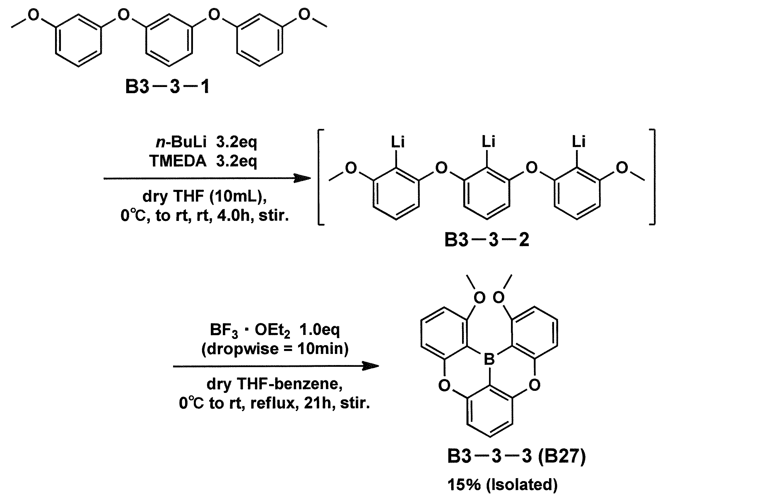
1-ヨード-3-メトキシベンゼンと1,3-ジヒドロキシベンゼンを原料として、銅触媒を利用したエーテル化反応を行い、トリフェニルエーテル体B3-3-1を収率95%で得た。
1-ヨード-3-メトキシベンゼンと1,3-ジヒドロキシベンゼンを原料として、銅触媒を利用したエーテル化反応を行い、トリフェニルエーテル体B3-3-1を収率95%で得た。
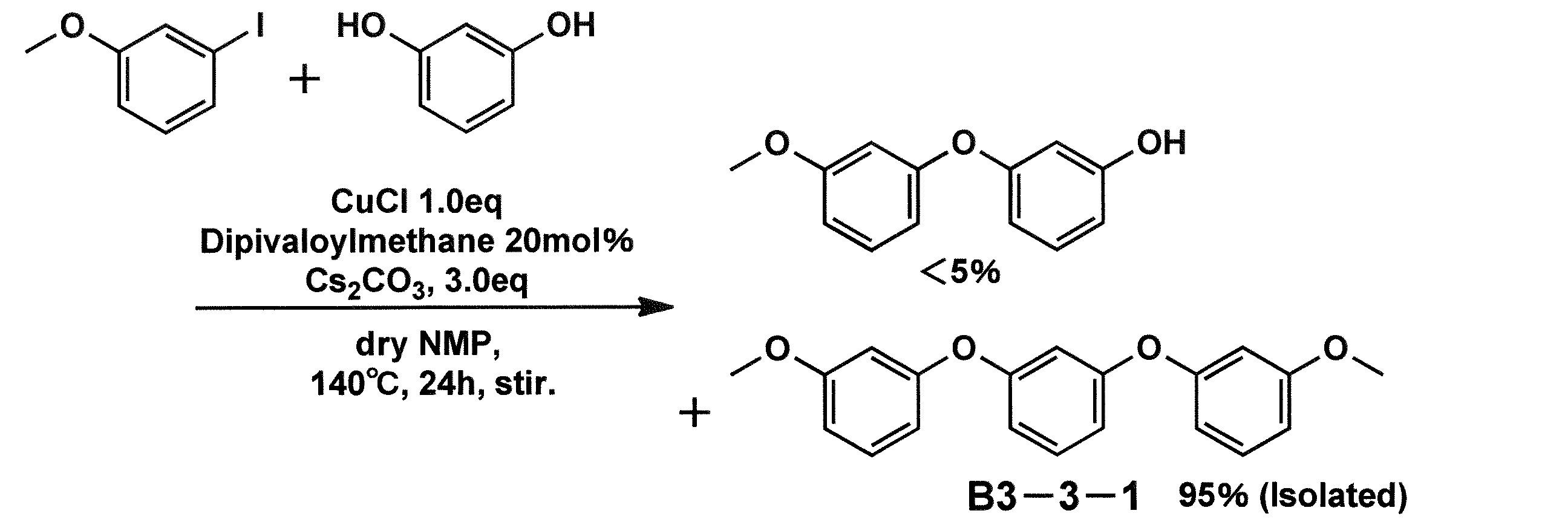
[スキーム2]
次に、B3-3-1にn-BuLiを滴下してトリリチオ化反応を行い、反応中間体としてB3-3-2が得られた。
続いて、ボリル化反応を行い、B3-3-2のTHF/ベンゼン混合溶液中に、1当量のBF3/OEt2を10分間かけて滴下した後、昇温して21時間加熱還流した。その後反応処理、精製を行うことで、B-3-3(B27)を収率15%で得た。
次に、B3-3-1にn-BuLiを滴下してトリリチオ化反応を行い、反応中間体としてB3-3-2が得られた。
続いて、ボリル化反応を行い、B3-3-2のTHF/ベンゼン混合溶液中に、1当量のBF3/OEt2を10分間かけて滴下した後、昇温して21時間加熱還流した。その後反応処理、精製を行うことで、B-3-3(B27)を収率15%で得た。
[スキーム3]
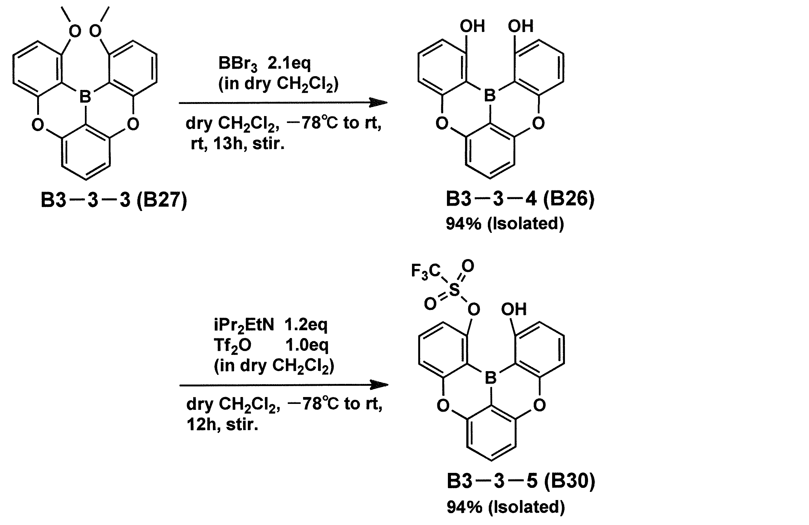
次に、BBr3を用いて脱保護を行った。-78℃の塩化メチレン溶液中に、BBr3を滴下していくことで、ホウ素-炭素結合が解離することなく、定量的に進行し、収率94%でB3-3-4(B26)を得た。
更に、B3-3-4(B26)の一つのカルボキシ基を、トリフルオロメタンスルホン酸無水物(Tf2O)を用いてスルホニル基に変換する反応を行い、収率94%でB3-3-5(B30)を得た。
次に、BBr3を用いて脱保護を行った。-78℃の塩化メチレン溶液中に、BBr3を滴下していくことで、ホウ素-炭素結合が解離することなく、定量的に進行し、収率94%でB3-3-4(B26)を得た。
更に、B3-3-4(B26)の一つのカルボキシ基を、トリフルオロメタンスルホン酸無水物(Tf2O)を用いてスルホニル基に変換する反応を行い、収率94%でB3-3-5(B30)を得た。
[スキーム4]
次に、塩基としてジアザビシクロウンデセン(1,8-diazabicyclo[5.4.0]undec-7-ene:DBU)を、溶媒としてN,N-ジメチルホルムアミド(N,N-dimethylformamide:DMF)を、マイクロ波(MW)を用いたマイクロリアクターを使用して240℃、4時間反応させることで、収率87%でB3を得た。
次に、塩基としてジアザビシクロウンデセン(1,8-diazabicyclo[5.4.0]undec-7-ene:DBU)を、溶媒としてN,N-ジメチルホルムアミド(N,N-dimethylformamide:DMF)を、マイクロ波(MW)を用いたマイクロリアクターを使用して240℃、4時間反応させることで、収率87%でB3を得た。

[有機ボラン錯体の合成]
室温にて、クロロホルム100部に、B3を1.00部、1,4-ジアザビシクロ[2.2.2]オクタン(DABCO)を0.20部加え3時間撹拌した。反応終了後、溶媒を減圧下で濃縮し、結晶が出てきたところで、濃縮を止め、そのまま室温で一晩静置した。得られた結晶を濾過し、冷クロロホルムで洗浄することで、B3-DABCO-B3を0.85部得た。
室温にて、クロロホルム100部に、B3を1.00部、1,4-ジアザビシクロ[2.2.2]オクタン(DABCO)を0.20部加え3時間撹拌した。反応終了後、溶媒を減圧下で濃縮し、結晶が出てきたところで、濃縮を止め、そのまま室温で一晩静置した。得られた結晶を濾過し、冷クロロホルムで洗浄することで、B3-DABCO-B3を0.85部得た。
(1H-NMRスペクトル解析)
上記で得られたB3-DABCO-B3の1H-NMR(重クロロホルム溶媒)を測定し、B3とDABCOの有機ボラン錯体であることを確認した(図4参照。)。
測定装置:Bruker Biospin AVANCE III 400 spect
rometer(400MHz for 1H-NMR)
測定条件:23℃(296K)、CDCl3溶媒使用、テトラメチルシラン基準(0ppm)
スペクトルデータ:B3(CDCl3,400MHz)δ:7.74(3H,t),7.22(6H,d)、DABCO(CDCl3,400MHz)δ:2.79(12H,s)、B3-DABCO-B3(CDCl3,400MHz)δ:7.13(3H,t),6.84(6H,d),3.01(12H,brs).
上記で得られたB3-DABCO-B3の1H-NMR(重クロロホルム溶媒)を測定し、B3とDABCOの有機ボラン錯体であることを確認した(図4参照。)。
測定装置:Bruker Biospin AVANCE III 400 spect
rometer(400MHz for 1H-NMR)
測定条件:23℃(296K)、CDCl3溶媒使用、テトラメチルシラン基準(0ppm)
スペクトルデータ:B3(CDCl3,400MHz)δ:7.74(3H,t),7.22(6H,d)、DABCO(CDCl3,400MHz)δ:2.79(12H,s)、B3-DABCO-B3(CDCl3,400MHz)δ:7.13(3H,t),6.84(6H,d),3.01(12H,brs).
(単結晶X線構造解析)
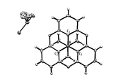
得られたB3-DABCO-B3の単結晶X線構造解析を行った。結果を図5に示す。B3部分のホウ素原子(B)と結合する炭素原子(C1~C3)との距離はそれぞれ、B-C1=1.562Å、B-C2=1.563Å、B-C3=1.567Åであった。
(結晶学データ:Monoclinic,C2/c,a=23.783(3)Å,b=9.9498(10)Å,c=18.2611(19)Å,β=113.2150(10)°,Z=8,d=1.538g/cm3,V=3971.42Å3,R1=0.0549,wR2=0.1538.)
一方、図6に示した例示化合物B3の単結晶X線構造解析の結果では、B-C1=1.459Å、B-C2=1.461Å、B-C3=1.459Åであった。
上記単結晶X線構造解析の結果から、配位結合を形成し得る物質であるDABCOとの反応により、トリアリールアミンB3におけるホウ素原子とアリール基上の炭素原子の結合が、SP2軌道からSP3軌道へ変化していることが分かる。
なお、単結晶X線構造解析は、以下の測定装置・測定条件で行った。
測定装置:Bruker Smart APEX II ULTRA
測定条件:測定温度/-173℃、線源/MoKα(λ=0.7103Å)、Data
integration and reduction/SAINT and XPREP software、Absorption correction/semiempirical method with SADABS、Structure /solved by direct method using SHELXL-97 and refined by using least-squares method on F2 with SHELXL-97.
得られたB3-DABCO-B3の単結晶X線構造解析を行った。結果を図5に示す。B3部分のホウ素原子(B)と結合する炭素原子(C1~C3)との距離はそれぞれ、B-C1=1.562Å、B-C2=1.563Å、B-C3=1.567Åであった。
(結晶学データ:Monoclinic,C2/c,a=23.783(3)Å,b=9.9498(10)Å,c=18.2611(19)Å,β=113.2150(10)°,Z=8,d=1.538g/cm3,V=3971.42Å3,R1=0.0549,wR2=0.1538.)
一方、図6に示した例示化合物B3の単結晶X線構造解析の結果では、B-C1=1.459Å、B-C2=1.461Å、B-C3=1.459Åであった。
上記単結晶X線構造解析の結果から、配位結合を形成し得る物質であるDABCOとの反応により、トリアリールアミンB3におけるホウ素原子とアリール基上の炭素原子の結合が、SP2軌道からSP3軌道へ変化していることが分かる。
なお、単結晶X線構造解析は、以下の測定装置・測定条件で行った。
測定装置:Bruker Smart APEX II ULTRA
測定条件:測定温度/-173℃、線源/MoKα(λ=0.7103Å)、Data
integration and reduction/SAINT and XPREP software、Absorption correction/semiempirical method with SADABS、Structure /solved by direct method using SHELXL-97 and refined by using least-squares method on F2 with SHELXL-97.
≪合成例2:B3-PY≫
室温にて、クロロホルム100部に、B3を1.00部と、ピリジンを0.28部加えて3時間撹拌した。反応終了後、溶媒を減圧下で濃縮し、結晶が出てきたところで、濃縮を止め、そのまま室温で一晩静置した。得られた結晶を濾過し、冷クロロホルムで洗浄することで、B3-PYを0.73部得た。
室温にて、クロロホルム100部に、B3を1.00部と、ピリジンを0.28部加えて3時間撹拌した。反応終了後、溶媒を減圧下で濃縮し、結晶が出てきたところで、濃縮を止め、そのまま室温で一晩静置した。得られた結晶を濾過し、冷クロロホルムで洗浄することで、B3-PYを0.73部得た。
(1H-NMRスペクトル解析)
得られたB3-PYの1H-NMR(重クロロホルム溶媒)を合成例1と同様にして測定したところ、原料であるB3由来のピークが消失し、新たな位置にピークが発生しており、B3-PYの有機ボラン錯体が生成したことを確認した。
得られたB3-PYの1H-NMR(重クロロホルム溶媒)を合成例1と同様にして測定したところ、原料であるB3由来のピークが消失し、新たな位置にピークが発生しており、B3-PYの有機ボラン錯体が生成したことを確認した。
≪耐熱性の比較≫
本発明のB3-PYと下記トリフェニルボランピリジン錯体を、それぞれ異なるガラスの封管に詰め、300℃に加熱した。B3-PYは、300℃、1時間の加熱後、ガラス管から取り出し、1H-NMRを測定したところ、全く分解していないことを確認した。
本発明のB3-PYと下記トリフェニルボランピリジン錯体を、それぞれ異なるガラスの封管に詰め、300℃に加熱した。B3-PYは、300℃、1時間の加熱後、ガラス管から取り出し、1H-NMRを測定したところ、全く分解していないことを確認した。

一方、トリフェニルボランピリジン錯体は、300℃、1時間の加熱後、1H-NMRを測定したところ、上記トリフェニルボランピリジン錯体とは異なる新たなピークが多数出現し、分解が起きていることを確認した。
また、本発明のB3-DABCO-B3を上記と同様の条件で耐熱性試験を行ったところ、全く分解していないことを確認した。
以上の結果から、本発明の化合物B3-PY、B3-DABCO-B3は従来公知のトリフェニルボランピリジン錯体と比べて十分な熱安定性を有することがわかった。
また、本発明のB3-DABCO-B3を上記と同様の条件で耐熱性試験を行ったところ、全く分解していないことを確認した。
以上の結果から、本発明の化合物B3-PY、B3-DABCO-B3は従来公知のトリフェニルボランピリジン錯体と比べて十分な熱安定性を有することがわかった。
≪有機EL素子における電子輸送材料としての使用≫
本発明の化合物B3-PYを電子輸送材料として使用し、有機EL素子を作製した。
陽極としてITO(インジウムスズ酸化物)を100nm成膜したガラス基板を、イソプロピルアルコールで超音波洗浄し、乾燥窒素ガスで乾燥及びUVオゾン洗浄を行い、真空蒸着装置の基板ホルダーに固定した。
真空蒸着装置内の真空度を1×10⁻⁴Paまで減圧した後、陽極の上に正孔注入層としてヘキサシアノヘキサアザトリフェニレン(15nm)、正孔輸送層としてα-NPD(4,4′-ビス〔N-(1-ナフチル)-N-フェニルアミノ〕ビフェニル)(30nm)をこの順番で形成した。
本発明の化合物B3-PYを電子輸送材料として使用し、有機EL素子を作製した。
陽極としてITO(インジウムスズ酸化物)を100nm成膜したガラス基板を、イソプロピルアルコールで超音波洗浄し、乾燥窒素ガスで乾燥及びUVオゾン洗浄を行い、真空蒸着装置の基板ホルダーに固定した。
真空蒸着装置内の真空度を1×10⁻⁴Paまで減圧した後、陽極の上に正孔注入層としてヘキサシアノヘキサアザトリフェニレン(15nm)、正孔輸送層としてα-NPD(4,4′-ビス〔N-(1-ナフチル)-N-フェニルアミノ〕ビフェニル)(30nm)をこの順番で形成した。
次いで発光層として、ホスト化合物である1,3-ビス(N-カルバゾリル)ベンゼン1,3-Bis(N-carbazolyl)benzene(mCP)及び発光性材料としてBis[2-(4,6-difluorophenyl)pyridinato-C2,N](picolinato)iridium(III)(FIrpic)を、mC
P:FIrpic=100:6の割合で共蒸着し、厚さ30nmの発光層を設けた。
P:FIrpic=100:6の割合で共蒸着し、厚さ30nmの発光層を設けた。
次いで電子輸送層として本発明の化合物B3-PY(15nm)、電子注入層としてフッ化リチウム(1.0nm)、陰極としてアルミニウム(100nm)をこの順番で蒸着し、有機EL素子を作製した。
得られた有機EL素子に、室温下、2.5mA/cm2の定電流を流したところ、青色に発光した。この結果から、本発明のB3-PYが有機EL素子における電子輸送材料として機能することが確認され、B3-PYが電荷伝導性を示すことが分かった。
得られた有機EL素子に、室温下、2.5mA/cm2の定電流を流したところ、青色に発光した。この結果から、本発明のB3-PYが有機EL素子における電子輸送材料として機能することが確認され、B3-PYが電荷伝導性を示すことが分かった。
≪有機EL素子における正孔輸送材料としての使用≫
本発明の化合物B3-PYを正孔輸送材料として使用し、有機EL素子を作製した。
陽極としてITOを100nm成膜したガラス基板を、イソプロピルアルコールで超音波洗浄し、乾燥窒素ガスで乾燥及びUVオゾン洗浄を行い、真空蒸着装置の基板ホルダーに固定した。
真空蒸着装置内の真空度を1×10⁻⁴Paまで減圧した後、陽極の上に正孔注入層としてヘキサシアノヘキサアザトリフェニレン(12nm)、正孔輸送層として本発明の化合物B3-DABCO-B3(40nm)をこの順番で形成した。
本発明の化合物B3-PYを正孔輸送材料として使用し、有機EL素子を作製した。
陽極としてITOを100nm成膜したガラス基板を、イソプロピルアルコールで超音波洗浄し、乾燥窒素ガスで乾燥及びUVオゾン洗浄を行い、真空蒸着装置の基板ホルダーに固定した。
真空蒸着装置内の真空度を1×10⁻⁴Paまで減圧した後、陽極の上に正孔注入層としてヘキサシアノヘキサアザトリフェニレン(12nm)、正孔輸送層として本発明の化合物B3-DABCO-B3(40nm)をこの順番で形成した。
次いで発光層に、ホスト化合物として1,3-Bis(N-carbazolyl)benzene(mCP)及び発光性材料としてBis[2-(4,6-difluorophenyl)pyridinato-C2,N](picolinato)iridium(III)(FIrpic)を、mCP:FIrpic=100:6の割合で共蒸着し
、厚さ30nmの発光層を設けた。
、厚さ30nmの発光層を設けた。
次いで電子輸送層として4,7-ジフェニル-1,10-フェナントロリン(BPhen)(30nm)、電子注入層としてフッ化リチウム(1.0nm)、陰極としてアルミニウム(100nm)をこの順番で蒸着し、有機EL素子を作製した。
得られた有機EL素子に、室温下、2.5mA/cm2の定電流を流したところ、青色に発光した。この結果から、本発明のB3-PYが有機EL素子における正孔輸送材料として機能することが確認され、B3-PYが電荷伝導性を示すことが分かった。
得られた有機EL素子に、室温下、2.5mA/cm2の定電流を流したところ、青色に発光した。この結果から、本発明のB3-PYが有機EL素子における正孔輸送材料として機能することが確認され、B3-PYが電荷伝導性を示すことが分かった。
本発明の有機ボラン錯体は、有機EL素子の発光層、正孔注入層、正孔輸送層、電子阻止層、正孔阻止層、電子輸送層、電子注入層及び中間層等の有機機能層に用いることができる。さらには、有機EL素子のみならず、太陽電池、トランジスタ等の様々な電子デバイスに用いることができる。
本発明の有機ボラン含有組成物は、有機EL素子中の有機機能層、有機光電変換素子中の有機機能層、トランジスタ中の有機機能層、電極・電荷移動性薄膜の他、インクジェット用インク、電子写真用トナー等に用いることができる。
本発明の有機ボラン含有組成物は、有機EL素子中の有機機能層、有機光電変換素子中の有機機能層、トランジスタ中の有機機能層、電極・電荷移動性薄膜の他、インクジェット用インク、電子写真用トナー等に用いることができる。
1 有機EL素子
2 透明基板
3 陽極
4 正孔注入層
5 正孔輸送層
6 発光層
7 電子輸送層
8 電子注入層
9 陰極
10 バルクヘテロジャンクション型の有機光電変換素子
11 基板
12 透明電極(陽極)
13 正孔輸送層
14 光電変換部(バルクヘテロジャンクション層)
15 電子輸送層
16 対極(陰極)
F 有機機能層
R 再結合
L 光
2 透明基板
3 陽極
4 正孔注入層
5 正孔輸送層
6 発光層
7 電子輸送層
8 電子注入層
9 陰極
10 バルクヘテロジャンクション型の有機光電変換素子
11 基板
12 透明電極(陽極)
13 正孔輸送層
14 光電変換部(バルクヘテロジャンクション層)
15 電子輸送層
16 対極(陰極)
F 有機機能層
R 再結合
L 光
Claims (6)
- 下記一般式(1)で表される構造を有するトリアリールボランを構成要素として含む有機ボラン錯体。
- 前記一般式(1)において、X3とX4が1個の原子となって連結しており、
該原子が、酸素原子又は硫黄原子である請求項1に記載の有機ボラン錯体。 - 前記一般式(1)で表される構造を有するトリアリールボランと、非共有電子対を有する化合物、金属又は金属化合物とを、構成成分として含む請求項1又は請求項2に記載の有機ボラン錯体。
- 前記一般式(1)で表される構造を有するトリアリールボランが、下記一般式(2)で表される構造を有するトリアリールボランである請求項1から請求項3までのいずれか一項に記載の有機ボラン錯体。

- 請求項1から請求項4までのいずれか一項に記載の有機ボラン錯体を含有する有機ボラン含有組成物。
- 請求項1から請求項4までのいずれか一項に記載の有機ボラン錯体を含有する有機機能層を有する有機エレクトロルミネッセンス素子。
Priority Applications (2)
| Application Number | Priority Date | Filing Date | Title |
|---|---|---|---|
| US16/334,686 US11708383B2 (en) | 2016-10-18 | 2017-09-28 | Organic borane complex, composition containing organic borane, and organic electroluminescent element |
| JP2018546214A JP7077950B2 (ja) | 2016-10-18 | 2017-09-28 | 有機ボラン錯体、有機ボラン含有組成物及び有機エレクトロルミネッセンス素子 |
Applications Claiming Priority (2)
| Application Number | Priority Date | Filing Date | Title |
|---|---|---|---|
| JP2016204632 | 2016-10-18 | ||
| JP2016-204632 | 2016-10-18 |
Publications (1)
| Publication Number | Publication Date |
|---|---|
| WO2018074167A1 true WO2018074167A1 (ja) | 2018-04-26 |
Family
ID=62018503
Family Applications (1)
| Application Number | Title | Priority Date | Filing Date |
|---|---|---|---|
| PCT/JP2017/035089 Ceased WO2018074167A1 (ja) | 2016-10-18 | 2017-09-28 | 有機ボラン錯体、有機ボラン含有組成物及び有機エレクトロルミネッセンス素子 |
Country Status (3)
| Country | Link |
|---|---|
| US (1) | US11708383B2 (ja) |
| JP (1) | JP7077950B2 (ja) |
| WO (1) | WO2018074167A1 (ja) |
Cited By (6)
| Publication number | Priority date | Publication date | Assignee | Title |
|---|---|---|---|---|
| WO2019074093A1 (ja) * | 2017-10-13 | 2019-04-18 | 学校法人関西学院 | 多環芳香族系二量体化合物 |
| WO2019235402A1 (ja) * | 2018-06-04 | 2019-12-12 | 学校法人関西学院 | 多環芳香族化合物およびその多量体 |
| CN111320643A (zh) * | 2020-03-04 | 2020-06-23 | Tcl华星光电技术有限公司 | 一种荧光化合物及其制作方法、显示模组 |
| KR20210122407A (ko) * | 2020-03-31 | 2021-10-12 | 삼성디스플레이 주식회사 | 유기 전계 발광 소자 및 유기 전계 발광 소자용 축합 다환 화합물 |
| US12371613B2 (en) | 2020-12-30 | 2025-07-29 | Samsung Display Co., Ltd. | Organic electroluminescence device and polycyclic compound for organic electroluminescence device |
| US12435267B2 (en) | 2020-10-16 | 2025-10-07 | Samsung Display Co., Ltd. | Organic electroluminescence device and polycyclic compound for organic electroluminescence device |
Families Citing this family (3)
| Publication number | Priority date | Publication date | Assignee | Title |
|---|---|---|---|---|
| KR102556834B1 (ko) | 2019-10-01 | 2023-07-19 | 삼성디스플레이 주식회사 | 유기 전계 발광 소자 |
| US20210119168A1 (en) * | 2019-10-01 | 2021-04-22 | Samsung Display Co., Ltd. | Organic electroluminescence device |
| US20220393109A1 (en) * | 2021-05-24 | 2022-12-08 | Samsung Electronics Co., Ltd. | Film and light-emitting device including the same |
Citations (4)
| Publication number | Priority date | Publication date | Assignee | Title |
|---|---|---|---|---|
| JP2011057990A (ja) * | 2010-10-08 | 2011-03-24 | Konica Minolta Holdings Inc | 有機エレクトロルミネッセンス素子用材料、有機エレクトロルミネッセンス素子、照明装置及び表示装置 |
| JP2013056859A (ja) * | 2011-09-08 | 2013-03-28 | Nagoya Univ | π共役有機ホウ素化合物及びその製造方法 |
| WO2016143624A1 (ja) * | 2015-03-09 | 2016-09-15 | 学校法人関西学院 | 多環芳香族化合物および発光層形成用組成物 |
| WO2016152418A1 (ja) * | 2015-03-25 | 2016-09-29 | 学校法人関西学院 | 多環芳香族化合物および発光層形成用組成物 |
Family Cites Families (6)
| Publication number | Priority date | Publication date | Assignee | Title |
|---|---|---|---|---|
| JP3889882B2 (ja) * | 1997-07-10 | 2007-03-07 | 三井化学株式会社 | オレフィン重合用触媒成分、オレフィン重合用触媒およびオレフィンの重合方法 |
| JP5338585B2 (ja) | 2009-09-11 | 2013-11-13 | 株式会社リコー | 液体吐出ヘッド及び画像形成装置 |
| JP6729589B2 (ja) * | 2015-07-24 | 2020-07-22 | コニカミノルタ株式会社 | 有機エレクトロルミネッセンス素子、表示装置及び照明装置 |
| WO2017092508A1 (zh) * | 2015-12-04 | 2017-06-08 | 广州华睿光电材料有限公司 | D-a型化合物及其应用 |
| CN106467553B (zh) * | 2016-07-29 | 2019-08-23 | 江苏三月光电科技有限公司 | 一种含硼有机电致发光化合物及其在oled器件上的应用 |
| US10686141B2 (en) * | 2016-09-07 | 2020-06-16 | Kwansei Gakuin Educational Foundation | Polycyclic aromatic compound |
-
2017
- 2017-09-28 US US16/334,686 patent/US11708383B2/en active Active
- 2017-09-28 WO PCT/JP2017/035089 patent/WO2018074167A1/ja not_active Ceased
- 2017-09-28 JP JP2018546214A patent/JP7077950B2/ja active Active
Patent Citations (4)
| Publication number | Priority date | Publication date | Assignee | Title |
|---|---|---|---|---|
| JP2011057990A (ja) * | 2010-10-08 | 2011-03-24 | Konica Minolta Holdings Inc | 有機エレクトロルミネッセンス素子用材料、有機エレクトロルミネッセンス素子、照明装置及び表示装置 |
| JP2013056859A (ja) * | 2011-09-08 | 2013-03-28 | Nagoya Univ | π共役有機ホウ素化合物及びその製造方法 |
| WO2016143624A1 (ja) * | 2015-03-09 | 2016-09-15 | 学校法人関西学院 | 多環芳香族化合物および発光層形成用組成物 |
| WO2016152418A1 (ja) * | 2015-03-25 | 2016-09-29 | 学校法人関西学院 | 多環芳香族化合物および発光層形成用組成物 |
Non-Patent Citations (1)
| Title |
|---|
| HIRAI, HIROKI ET AL.: "One-step borylation of 1, 3-diaryloxybenzenes towards efficient materials for organic light-emitting diodes", ANGEWANDTE CHEMIE , INTERNATIONAL EDITION, vol. 54, no. 46, 2015, pages 13581 - 13585, XP055310723 * |
Cited By (8)
| Publication number | Priority date | Publication date | Assignee | Title |
|---|---|---|---|---|
| WO2019074093A1 (ja) * | 2017-10-13 | 2019-04-18 | 学校法人関西学院 | 多環芳香族系二量体化合物 |
| WO2019235402A1 (ja) * | 2018-06-04 | 2019-12-12 | 学校法人関西学院 | 多環芳香族化合物およびその多量体 |
| CN111320643A (zh) * | 2020-03-04 | 2020-06-23 | Tcl华星光电技术有限公司 | 一种荧光化合物及其制作方法、显示模组 |
| KR20210122407A (ko) * | 2020-03-31 | 2021-10-12 | 삼성디스플레이 주식회사 | 유기 전계 발광 소자 및 유기 전계 발광 소자용 축합 다환 화합물 |
| US12426499B2 (en) | 2020-03-31 | 2025-09-23 | Samsung Display Co., Ltd. | Organic electroluminescence device and fused polycyclic compound for organic electroluminescence device |
| KR102922215B1 (ko) | 2020-03-31 | 2026-02-04 | 삼성디스플레이 주식회사 | 유기 전계 발광 소자 및 유기 전계 발광 소자용 축합 다환 화합물 |
| US12435267B2 (en) | 2020-10-16 | 2025-10-07 | Samsung Display Co., Ltd. | Organic electroluminescence device and polycyclic compound for organic electroluminescence device |
| US12371613B2 (en) | 2020-12-30 | 2025-07-29 | Samsung Display Co., Ltd. | Organic electroluminescence device and polycyclic compound for organic electroluminescence device |
Also Published As
| Publication number | Publication date |
|---|---|
| US20210292342A1 (en) | 2021-09-23 |
| JP7077950B2 (ja) | 2022-05-31 |
| JPWO2018074167A1 (ja) | 2019-09-05 |
| US11708383B2 (en) | 2023-07-25 |
Similar Documents
| Publication | Publication Date | Title |
|---|---|---|
| WO2018074167A1 (ja) | 有機ボラン錯体、有機ボラン含有組成物及び有機エレクトロルミネッセンス素子 | |
| US11444254B2 (en) | Metal complexes comprising diazabenzmidazolocarbene ligands and the use thereof in OLEDs | |
| Wang et al. | High‐Performance Red, Green, and Blue Electroluminescent Devices Based on Blue Emitters with Small Singlet–Triplet Splitting and Ambipolar Transport Property | |
| Chen et al. | Rational design of strongly blue-emitting cuprous complexes with thermally activated delayed fluorescence and application in solution-processed OLEDs | |
| Zhang et al. | Towards high efficiency and low roll‐off orange electrophosphorescent devices by fine tuning singlet and triplet energies of bipolar hosts based on indolocarbazole/1, 3, 5‐triazine hybrids | |
| KR102165718B1 (ko) | π 공액계 붕소 화합물, 전자 디바이스, 및 트리아릴보란과 그의 중간체의 제조 방법 | |
| Shanmugasundaram et al. | Green electroluminescence from charged phenothiazine derivative | |
| Gong et al. | Solution-processed double-silicon-bridged oxadiazole/arylamine hosts for high-efficiency blue electrophosphorescence | |
| Li et al. | Brightly fluorescent red organic solids bearing boron-bridged π–conjugated skeletons | |
| Xu et al. | A novel deep blue-emitting znii complex based on carbazole-modified 2-(2-hydroxyphenyl) benzimidazole: Synthesis, bright electroluminescence, and substitution effect on photoluminescent, thermal, and electrochemical properties | |
| JP2023543421A (ja) | 青色光を発光する有機エレクトロルミネッセンス素子 | |
| TWI801524B (zh) | 用於光電器件的有機分子 | |
| WO2018230860A1 (ko) | 신규한 화합물 및 이를 포함하는 유기 발광소자 | |
| Wang et al. | Manipulation of thermally activated delayed fluorescence of blue exciplex emission: fully utilizing exciton energy for highly efficient organic light emitting diodes with low roll-off | |
| Gong et al. | Extension of molecular structure toward solution-processable hosts for efficient blue phosphorescent organic light-emitting diodes | |
| TW201928010A (zh) | 用於光電器件的有機分子 | |
| CN109415317A (zh) | 用于光电器件的二咔唑联苯衍生物 | |
| Aghazada et al. | Molecular Engineering of Iridium Blue Emitters Using Aryl N‐Heterocyclic Carbene Ligands | |
| CN104685650B (zh) | 用作有机电子器件的n型掺杂剂的环戊二烯的盐 | |
| Bossi et al. | Benzodithienyl Silanes for Organic Electronics: AIE Solid‐State Blue Emitters and High Triplet Energy Charge‐Transport Materials | |
| JP7772051B2 (ja) | トリアリールホウ素化合物、有機エレクトロルミネッセンス素子、表示装置及び照明装置 | |
| Earnhardt | Hypercoordinate Silicon CNC-Pincer Complexes for Electronic Devices | |
| JP2025505549A (ja) | 光電子素子用有機分子 | |
| Rao | Optoeletronic properties and photochemical reactivitiy of organoboron compounds | |
| McCormick | Luminescent Transition Metal Complexes of 2-(2’-Pyridyl) Benzimidazolyl and 2-(2’-Pyridyl) Indolyl Based Ligands and Their Applications |
Legal Events
| Date | Code | Title | Description |
|---|---|---|---|
| 121 | Ep: the epo has been informed by wipo that ep was designated in this application |
Ref document number: 17861569 Country of ref document: EP Kind code of ref document: A1 |
|
| ENP | Entry into the national phase |
Ref document number: 2018546214 Country of ref document: JP Kind code of ref document: A |
|
| NENP | Non-entry into the national phase |
Ref country code: DE |
|
| 122 | Ep: pct application non-entry in european phase |
Ref document number: 17861569 Country of ref document: EP Kind code of ref document: A1 |