WO2018074084A1 - 半導体デバイスおよび表示装置ならびに電子機器 - Google Patents
半導体デバイスおよび表示装置ならびに電子機器 Download PDFInfo
- Publication number
- WO2018074084A1 WO2018074084A1 PCT/JP2017/031931 JP2017031931W WO2018074084A1 WO 2018074084 A1 WO2018074084 A1 WO 2018074084A1 JP 2017031931 W JP2017031931 W JP 2017031931W WO 2018074084 A1 WO2018074084 A1 WO 2018074084A1
- Authority
- WO
- WIPO (PCT)
- Prior art keywords
- substrate
- actuator
- semiconductor device
- display device
- structures
- Prior art date
- Legal status (The legal status is an assumption and is not a legal conclusion. Google has not performed a legal analysis and makes no representation as to the accuracy of the status listed.)
- Ceased
Links
Images











Classifications
-
- B—PERFORMING OPERATIONS; TRANSPORTING
- B81—MICROSTRUCTURAL TECHNOLOGY
- B81B—MICROSTRUCTURAL DEVICES OR SYSTEMS, e.g. MICROMECHANICAL DEVICES
- B81B3/00—Devices comprising flexible or deformable elements, e.g. comprising elastic tongues or membranes
- B81B3/0018—Structures acting upon the moving or flexible element for transforming energy into mechanical movement or vice versa, i.e. actuators, sensors, generators
- B81B3/0021—Transducers for transforming electrical into mechanical energy or vice versa
-
- G—PHYSICS
- G02—OPTICS
- G02B—OPTICAL ELEMENTS, SYSTEMS OR APPARATUS
- G02B26/00—Optical devices or arrangements for the control of light using movable or deformable optical elements
- G02B26/08—Optical devices or arrangements for the control of light using movable or deformable optical elements for controlling the direction of light
- G02B26/0816—Optical devices or arrangements for the control of light using movable or deformable optical elements for controlling the direction of light by means of one or more reflecting elements
- G02B26/0833—Optical devices or arrangements for the control of light using movable or deformable optical elements for controlling the direction of light by means of one or more reflecting elements the reflecting element being a micromechanical device, e.g. a MEMS mirror, DMD
- G02B26/0858—Optical devices or arrangements for the control of light using movable or deformable optical elements for controlling the direction of light by means of one or more reflecting elements the reflecting element being a micromechanical device, e.g. a MEMS mirror, DMD the reflecting means being moved or deformed by piezoelectric means
-
- G—PHYSICS
- G02—OPTICS
- G02B—OPTICAL ELEMENTS, SYSTEMS OR APPARATUS
- G02B27/00—Optical systems or apparatus not provided for by any of the groups G02B1/00 - G02B26/00, G02B30/00
- G02B27/01—Head-up displays
- G02B27/017—Head mounted
- G02B27/0172—Head mounted characterised by optical features
-
- G—PHYSICS
- G02—OPTICS
- G02B—OPTICAL ELEMENTS, SYSTEMS OR APPARATUS
- G02B30/00—Optical systems or apparatus for producing three-dimensional [3D] effects, e.g. stereoscopic images
- G02B30/20—Optical systems or apparatus for producing three-dimensional [3D] effects, e.g. stereoscopic images by providing first and second parallax images to an observer's left and right eyes
-
- H—ELECTRICITY
- H04—ELECTRIC COMMUNICATION TECHNIQUE
- H04N—PICTORIAL COMMUNICATION, e.g. TELEVISION
- H04N13/00—Stereoscopic video systems; Multi-view video systems; Details thereof
- H04N13/30—Image reproducers
- H04N13/332—Displays for viewing with the aid of special glasses or head-mounted displays [HMD]
- H04N13/344—Displays for viewing with the aid of special glasses or head-mounted displays [HMD] with head-mounted left-right displays
-
- B—PERFORMING OPERATIONS; TRANSPORTING
- B81—MICROSTRUCTURAL TECHNOLOGY
- B81B—MICROSTRUCTURAL DEVICES OR SYSTEMS, e.g. MICROMECHANICAL DEVICES
- B81B2201/00—Specific applications of microelectromechanical systems
- B81B2201/03—Microengines and actuators
- B81B2201/032—Bimorph and unimorph actuators, e.g. piezo and thermo
-
- B—PERFORMING OPERATIONS; TRANSPORTING
- B81—MICROSTRUCTURAL TECHNOLOGY
- B81B—MICROSTRUCTURAL DEVICES OR SYSTEMS, e.g. MICROMECHANICAL DEVICES
- B81B2201/00—Specific applications of microelectromechanical systems
- B81B2201/04—Optical MEMS
- B81B2201/047—Optical MEMS not provided for in B81B2201/042 - B81B2201/045
-
- B—PERFORMING OPERATIONS; TRANSPORTING
- B81—MICROSTRUCTURAL TECHNOLOGY
- B81B—MICROSTRUCTURAL DEVICES OR SYSTEMS, e.g. MICROMECHANICAL DEVICES
- B81B2203/00—Basic microelectromechanical structures
- B81B2203/05—Type of movement
- B81B2203/053—Translation according to an axis perpendicular to the substrate
-
- B—PERFORMING OPERATIONS; TRANSPORTING
- B81—MICROSTRUCTURAL TECHNOLOGY
- B81B—MICROSTRUCTURAL DEVICES OR SYSTEMS, e.g. MICROMECHANICAL DEVICES
- B81B2207/00—Microstructural systems or auxiliary parts thereof
- B81B2207/05—Arrays
- B81B2207/053—Arrays of movable structures
-
- G—PHYSICS
- G02—OPTICS
- G02B—OPTICAL ELEMENTS, SYSTEMS OR APPARATUS
- G02B27/00—Optical systems or apparatus not provided for by any of the groups G02B1/00 - G02B26/00, G02B30/00
- G02B27/01—Head-up displays
- G02B27/0101—Head-up displays characterised by optical features
- G02B2027/0132—Head-up displays characterised by optical features comprising binocular systems
- G02B2027/0134—Head-up displays characterised by optical features comprising binocular systems of stereoscopic type
-
- G—PHYSICS
- G03—PHOTOGRAPHY; CINEMATOGRAPHY; ANALOGOUS TECHNIQUES USING WAVES OTHER THAN OPTICAL WAVES; ELECTROGRAPHY; HOLOGRAPHY
- G03B—APPARATUS OR ARRANGEMENTS FOR TAKING PHOTOGRAPHS OR FOR PROJECTING OR VIEWING THEM; APPARATUS OR ARRANGEMENTS EMPLOYING ANALOGOUS TECHNIQUES USING WAVES OTHER THAN OPTICAL WAVES; ACCESSORIES THEREFOR
- G03B35/00—Stereoscopic photography
- G03B35/18—Stereoscopic photography by simultaneous viewing
-
- H—ELECTRICITY
- H04—ELECTRIC COMMUNICATION TECHNIQUE
- H04N—PICTORIAL COMMUNICATION, e.g. TELEVISION
- H04N13/00—Stereoscopic video systems; Multi-view video systems; Details thereof
- H04N13/30—Image reproducers
- H04N13/388—Volumetric displays, i.e. systems where the image is built up from picture elements distributed through a volume
- H04N13/395—Volumetric displays, i.e. systems where the image is built up from picture elements distributed through a volume with depth sampling, i.e. the volume being constructed from a stack or sequence of two-dimensional [2D] image planes
Definitions
- the present disclosure relates to, for example, a semiconductor device used in a stereoscopic image display apparatus, a display apparatus including the semiconductor device, and an electronic apparatus.
- a screen is arranged at a position of a real image, and the depth position of a virtual image is changed by moving the screen in the depth direction in units of pixels.
- the depth position of the virtual image can be varied within a range from several tens cm to near infinity.
- the displacement in the depth direction of the screen for each pixel is mainly realized by MEMS (Micro Electro Mechanical Systems) (see, for example, Patent Document 1).
- a semiconductor device includes a substrate, a plurality of structures that are arranged in a matrix and have a planar portion, and a plurality of structures that are arranged on the substrate, and each of the plurality of structures is a substrate. And a plurality of piezoelectric actuators that move in a direction perpendicular to the surface.
- a display device includes an optical system including a lens and a display device, and includes the semiconductor device according to the embodiment described above as a display device.
- An electronic apparatus includes the display device according to the above-described embodiment.
- each of the plurality of structures having a planar portion is arranged along a direction perpendicular to one surface of the substrate. It arrange
- one surface of the substrate is provided between the plurality of structures having the planar portion and the substrate. Since a plurality of piezoelectric actuators that are moved along the vertical direction are arranged, the distance of a plurality of structures having a planar portion to one surface of the substrate can be greatly varied. In addition, since the plurality of piezoelectric actuators are disposed in each of the plurality of structures having the planar portion, the variation in the distance of the plurality of structures having the planar portion with respect to one surface of the substrate is independently determined. Can be done. That is, a large variation along the direction perpendicular to the in-plane with a small pitch is possible.
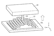
- FIG. 2 is a perspective view illustrating an example of a configuration of a display element illustrated in FIG. 1. It is a perspective view showing the other example of a structure of the display element shown in FIG. It is sectional drawing showing an example of a structure of the actuator shown in FIG.
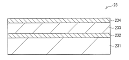
- FIG. 7 is a cross-sectional view illustrating another example of the configuration of the actuator illustrated in FIG. 1.
- FIG. 2 is a schematic plan view illustrating a configuration of the actuator illustrated in FIG. 1. It is a schematic diagram explaining the deformation
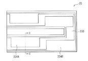
- FIG. 2 is a plan view illustrating an example of a configuration of an actuator illustrated in FIG. 1.
- FIG. 3 is a perspective view for explaining the movement of the display element shown in FIG. 2.
- FIG. 10 is a plan view illustrating another example of the configuration of the actuator illustrated in FIG. 1.
- FIG. 10 is a perspective view for explaining the movement of the display element shown in FIG. 9.
- FIG. 2 is a schematic plan view illustrating an example of wiring routing of the actuator illustrated in FIG. 1.
- FIG. 11B is a schematic cross-sectional view showing the wiring routing of the actuator shown in FIG. 11A.
- FIG. 7 is a schematic plan view illustrating another example of the wiring routing of the actuator illustrated in FIG. 1.
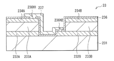
- FIG. 12B is a schematic cross-sectional view showing wiring routing of the actuator shown in FIG. 12A. It is a block diagram showing the structure of the display apparatus of this indication.
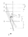
- FIG. 14 It is a schematic diagram explaining the optical system in the display apparatus shown in FIG. 14 is a perspective view illustrating an example of a configuration of a display element according to Modification 1 of the present disclosure.
- FIG. 14 is a perspective view illustrating another example of a configuration of a display element according to Modification Example 1 of the present disclosure.
- FIG. 17 is a plan view for explaining the arrangement of the display elements shown in FIG. 16. It is a perspective view showing the composition of the display element concerning modification 2 of this indication. It is a perspective view showing the appearance of the head mounted display concerning an application example.
- Embodiment (Example of display device that moves the screen surface using a piezoelectric actuator) 1-1. Configuration of display device 1-2. Configuration of display device 1-3. Action / Effect Modification 2-1. Modification 1 (example using actuators having different widths along two directions orthogonal to each other) 2-2. Modification 2 (example using an actuator having a multilayer structure) 3.
- Application examples
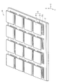
- FIG. 1 is a perspective view of a semiconductor device (display device 10) according to an embodiment of the present disclosure, and schematically shows the configuration thereof.
- FIG. 2 is a perspective view of the display element 20A shown in FIG. 1, and schematically shows the configuration thereof.
- the display device 10 is used for, for example, a display device (display device 1) capable of displaying a stereoscopic image described later.
- the display device 10 according to the present embodiment is arranged in a matrix on the substrate 21 and a plurality of structures (structures 22) having, for example, a plane portion (plane portion 22A) serving as a screen surface. And a plurality of piezoelectric actuators (actuators 23) respectively disposed between the substrate 21 and the plurality of structures 22.
- the display device 10 includes a plurality of display elements 20A including the structure 22 and the actuators 23 arranged between the substrate 21 and the structure 22 on the substrate 21, for example, in a matrix form. Is arranged.
- a structural body 22 is connected to the actuator 23 via, for example, a connecting portion 24. By driving the actuator 23, the structural body 22 moves in a direction perpendicular to the surface of the substrate 21 (Z-axis direction). It is possible.
- the substrate 21 is for supporting the actuator 23 and the structure 22 connected thereto.
- the substrate 21 is preferably not easily deformed, that is, has a high rigidity, and is made of, for example, a silicon wafer.
- the substrate 21 has an opening at a position corresponding to the display element 20.
- the opening may be a concave shape that opens from the surface opposite to the surface (element forming surface) on which the display element 20 is formed toward the element forming surface, and the substrate 21 remains on the bottom.
- a through-hole shape penetrating the substrate 21 may be used. In the case where a sacrificial layer or the like is provided between the substrate 21 and the actuator 23 and a sufficient space can be secured between the substrate 21 and the actuator 23, the opening may not be provided.
- the structure 22 is a plate-like member having the flat portion 22A as described above.
- the flat portion 22A functions as, for example, a screen surface, and the surface thereof preferably has light reflectivity.
- the planar portion 22A reflects light incident on the structure 22 from the Z-axis direction, for example, when reflecting incident light only in one direction, such as a mirror surface, the pupil diameter is very small.
- the planar portion 22A is preferably a light diffusing surface that diffuses incident light at a wide angle.
- the planar portion 22A is preferably a rough surface having random irregularities on the surface. Thereby, a robust optical system can be realized in the display device 1 described later.
- the structure 22 is made of, for example, polysilicon having a reflective film such as aluminum (Al) formed on the surface. As described above, a plurality of the structures 22 are arranged in a matrix on the substrate 21, and each structure 22 constitutes one pixel.
- one or a plurality of light emitting elements 25 such as micro LEDs (Light25Emitting Diode), for example, red (R), green (You may make it mount three light emitting elements of G) and blue (B).
- micro LEDs Light25Emitting Diode
- R red
- G green
- B blue
- the actuator 23 moves the structure 22 along the direction perpendicular to the surface of the substrate 21 (Z-axis direction), and changes the distance between the planar portion 22A of the structure 22 and the substrate 21.
- the plurality of actuators 23 arranged on the substrate 21 are formed at positions corresponding to the pixels of the actuator layer 23L provided on the substrate 21, respectively.
- the actuator 23 is, for example, a cantilever type piezoelectric actuator, one end of which is fixed to the substrate 21, and the other end of the structure 23 is connected via a connecting portion 24. For example, as shown in FIG.
- the actuator 23 has a so-called unimorph structure in which a first electrode film 232, a piezoelectric film 233, and a second electrode film 234 are laminated in this order on a support member 231.
- the actuator 23 may have a so-called bimorph structure in which two piezoelectric films (piezoelectric films 233A and 233B) are stacked on a support member 231 as shown in FIG. 5, for example.
- the bimorph actuator 23 has, for example, a configuration in which a first electrode film 232, a piezoelectric film 233A, a third electrode film 235, a piezoelectric film 233B, and a second electrode film 234 are stacked in this order on a support member 231.
- the piezoelectric films 233 ⁇ / b> A and 233 ⁇ / b> B are applied with voltages that are inverted with each other, whereby a large generated force is obtained and a larger displacement amount is obtained.
- a protective film (a protective film 236 (for example, see FIG. 11B)) is provided over the second electrode film 234 as necessary.
- the actuator 23 is a cantilever type in which an electrode film (for example, the second electrode film 224) on one surface of the piezoelectric film 223 is configured by a pair of electrodes (electrodes 234A and 234B) to which a reverse polarity voltage can be applied.
- the piezoelectric actuator is configured as one unit and a plurality of the piezoelectric actuators are connected in series. As a result, the actuator 23 can achieve a relatively large stroke of several tens of ⁇ m or more with a small footprint of, for example, several tens of ⁇ m.
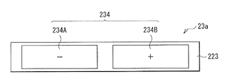
- the cantilever-type piezoelectric actuator 1 unit 23a has a rectangular shape extending in one axial direction (for example, the X-axis direction) as shown in FIG. 6A, for example, and one surface (for example, the second electrode) of the piezoelectric film 233 As described above, two electrodes (electrodes 234A and 234B) for applying a reverse polarity voltage are provided in the membrane side). That is, the second electrode film 234 shown in FIGS. 4 and 5 includes two electrodes 234A and 234B.
- the piezoelectric film 233 corresponds to the electrode 234A, for example, as shown in FIG. 6B.
- the first electrode film 232 side contracts, and in the region corresponding to the electrode 234B, for example, the electrode 234B side contracts.
- the piezoelectric film 233 is warped and deformed in the Z-axis direction.
- the planar portion 22A of the structure 22 connected to the other end of the actuator 23 having one end fixed to the substrate 21 is movable in the direction perpendicular to the surface of the substrate 21 (XY plane) (Z-axis direction).
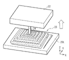
- the actuator 23 has a plurality of units 23a1 to 23an connected in series in a spiral shape as shown in FIG. 7, for example.
- the plurality of units are connected so that two electrodes to which a reverse polarity voltage is applied are alternately arranged.
- one end of a plurality of units 23a (unit 23a1 in FIG. 7) connected in series is fixed to the substrate 21, and the other end (unit 23an in FIG. 7) has a structure.
- a holding portion 23 ⁇ / b> X for holding 22 is provided, and the structure 22 is held by the holding portion 23 ⁇ / b> X via the connection portion 24.
- the height of the planar portion 22A of the structure 22 with respect to the surface of the substrate 21 can be greatly displaced in the Z-axis direction by the amount of the units constituting the actuator 23, as shown in FIG.
- the actuator 23 shows only its outer frame, and the notation of the electrodes 234A and 234B is omitted. The same applies to FIG. 10, FIG. 15, FIG. 16, and FIG.
- the actuator 23 is preferably connected in series in a meander shape, for example, as shown in FIG.
- the holding portion 23X is arranged at the center of the units 23a arranged in parallel in the X-axis direction, and the structure 22 is connected to the holding portion 23X via the connection portion 24.
- the plurality of units 23a are connected so that two electrodes to which a reverse polarity voltage is applied are alternately arranged toward one end fixed to the substrate 21 starting from the holding portion 23X. It is preferable. Thereby, the planar portion 22A of the structure 22 can be largely displaced in the Z-axis direction as shown in FIG.
- the wiring structure of the electrodes 234A and 234B may be patterned on the piezoelectric film 223 as shown in FIGS. 11A and 11B, for example.
- FIG. 11B shows a cross-sectional structure of the actuator 23 along the line II-II in FIG. 11A.
- the wiring structure of the electrode 234A and the electrode 234B has, for example, a first electrode film 232 (electrode 232A), a piezoelectric film 233A, and a second electrode film, respectively, in the unit as shown in FIGS. 12A and 12B.
- Electrode 234A), the first electrode film (electrode 232B), the piezoelectric film 233B, and the second electrode film (electrode 234B) each form two stacked bodies in this order, and one second electrode (for example, The electrode 234A) and the other first electrode (for example, the electrode 232B) may be electrically connected through the conductive film 237.
- FIG. 12B shows a cross-sectional structure of the actuator 23 along the line III-III in FIG. 12A.
- the two laminates and the support member 231 are covered with a protective film 236.
- the protective film 236 has openings 236H1 and 236H2 on the electrode 234A and on the electrode 232B extending to the adjacent stacked body, respectively.
- the conductive film 237 is connected to the electrode 234A and the electrode through the openings 236H1 and 236H2.
- 232B is electrically connected to each other. Note that the routing structure shown in FIGS. 12A and 12B can maximize the area of the electrode 234A and the electrode 234B, so that a large generating force can be obtained.
- connection unit 24 is for connecting the structure 22 to the actuator 23.
- the connection part 24 preferably has insulating properties, and is preferably made of, for example, silicon nitride (SiN).
- the length (l) of the connecting portion 24 is preferably larger than, for example, the variable distance of the planar portion 22A of the structure 22 with respect to the surface of the substrate 21, that is, the displacement amount of the actuator 23 in the Z-axis direction.
- a structure 22 of a plurality of display elements 30B each having a sufficiently large one of the widths along two directions orthogonal to each other is shown in FIG.
- the initial value of the structure 22 is, for example, the distance from the surface of the substrate 21 to the planar portion 22A of the structure 22 when the actuator 33B is not driven.
- the display element 20 applies a voltage having an opposite phase to the actuator 23 to reduce the distance between the surface of the substrate 21 and the planar portion 22A of the structure 22, that is, the plane of the structure 22.
- the portion 22A can be moved toward the substrate 21 in the Z-axis direction.
- the length of the connecting portion 24 is set larger than the displacement amount of the actuator 33B in the Z-axis direction, thereby preventing interference between the structure 22 and the actuator 23 between adjacent pixels. be able to.
- the actuator 23 is disposed between the substrate 21 and the structure 22 having the planar portion 22A, and one end of the actuator 23 is fixed to the substrate 21. Since the structure 22 is connected to the end via the connection portion 24, the position of the planar portion 22A of the structure 22 varies greatly in the direction perpendicular to the surface of the substrate 21 (Z-axis direction) for each pixel. It becomes possible to make it.
- the display device 10 according to the present embodiment can realize a screen array movable for each pixel by individually controlling the driving of each actuator 23 of each display element 20A.
- FIG. 13 illustrates a configuration of the display device 1 of the present disclosure.
- the display device 1 is a display device that can display a stereoscopic image.
- the display device 1 includes, for example, an image processing unit 100 and an image display unit 200.
- the image processing unit 100 analyzes binocular parallax included in a stereoscopic video and acquires depth information of an object shown in the stereoscopic video. Specifically, the object setting unit 110 acquires the depth information of the object included in the stereoscopic video together with the parallax image for the right eye and the parallax image for the left eye included in the stereoscopic video.
- the partial area generation unit 120 divides the stereoscopic video to be processed into a plurality of partial areas based on the depth information acquired by the object setting unit 110.
- the rendering unit 130 generates an image composed of pixels included in each of the partial areas generated by the partial area generation unit 120.
- the image display unit 200 presents the image acquired by the image processing unit 100 to a user who observes the display device 1.
- the virtual image position setting unit 210 based on the depth information acquired by the object setting unit 110, the position at which the virtual image of the image generated by the rendering unit 130 is displayed, that is, the screen 22 is the structure 22 in the present embodiment.
- the position of the plane portion 22A is set.
- the virtual image display unit 220 presents a virtual image to the user observing the display device 1 based on the image acquired by the image processing unit 100.
- FIG. 14 schematically shows a configuration of an optical system included in the display device 1.
- the display device 1 includes, for example, a convex lens 310 and the display device 10 as an optical system.
- the convex lens 310 and the display device 10 have a Z axis determined in the line-of-sight direction of the viewpoint 300, and are arranged on the Z axis so that the optical axis of the convex lens 310 and the Z axis coincide.
- the screen surface (the planar portion 22 ⁇ / b> A of the structure) is disposed at a distance A (A ⁇ F) in front of the focal length F of the convex lens 27.
- the display device 10 is disposed inside the focal point of the convex lens 27. At this time, from the viewpoint 300, the image displayed on the display device 10 is observed as a virtual image at a position away from the convex lens 27 by a distance B (F ⁇ B).
- the position of the screen surface (plane portion 22A) of the display device 10 of the present embodiment varies in the Z-axis direction.
- the position of the virtual image of the real image 311a displayed on the plane portion 22A is changed by moving the plane portion 22A by the distance A1 or the distance A2 along the Z axis toward the user side (viewpoint 300 side).
- the distance from the position 312 a to the user side can be changed by a distance B1 (virtual image 312 b) and a distance B2 (virtual image 312 c).
- the display device 10 according to the present embodiment can vary the planar portion 22A for each pixel, for example, several tens of ⁇ m.
- the position of the virtual image observed from the viewpoint 300 can be changed more greatly. That is, distance information from several tens of centimeters to infinity can be reproduced for each pixel.
- the pixel size is as small as several tens of micrometers, and a shape change (vertical stroke) of several tens of micrometers is required for this pixel size.
- a shape change (vertical stroke) of several tens of micrometers is required for this pixel size.
- MEMES device that realizes the vertical stroke as described above, and it is desired to develop a MEMES device that can change in the vertical direction of several tens of ⁇ m at a small pitch (several tens of ⁇ m). ing.
- the plurality of structures 22 having the planar portion 22A are respectively moved through the plurality of actuators 23 that move along the direction perpendicular to the surface of the substrate 21. 11 is arranged in a matrix, for example. Thereby, it is possible to independently perform the variation in the vertical direction (Z-axis direction) with respect to the surface of the substrate 21 of the plurality of structures 22 having the planar portion 22A with a large stroke.
- the plurality of actuators 23 that are moved along the direction perpendicular to the surface of the substrate 21 are arranged between the plurality of structures 22 having the planar portion 22A and the substrate 21, respectively. I made it. Thereby, the distance between the planar portion 22A of the structure 22 and the surface of the substrate 21 can be greatly varied.
- the actuators 23 are individually arranged in each of the plurality of structures 22 having the planar portion 22A, the variation in distance from the surface of the substrate 21 of the plurality of structures 22 having the planar portion 22A is independent of each other. Can be performed. Therefore, it is possible to greatly change the plane portion 22A along the direction perpendicular to the in-plane with a small pitch. That is, when the planar portion 22A is formed as a screen surface, it is possible to provide a stereoscopic image display device that can reproduce depth information of several tens of centimeters to infinity by a virtual image for each pixel.
- a cantilever-type piezoelectric actuator is formed as one unit, and a plurality of them are connected in series.
- the actuator 23 can change in a large vertical direction with respect to the surface of the substrate 21 of several tens of ⁇ m or more, for example, with a small footprint of about several tens of ⁇ m. Therefore, it is possible to provide both a large stroke and a small pixel size, and it is possible to provide a stereoscopic image display device with higher image quality.
- a display device capable of stereoscopic display with a simpler optical system can be realized.
- FIG. 1 15 and 16 are perspective views of a display element (display elements 30A and 30B) according to a modified example (modified example 1) of the present disclosure, and schematically illustrate the configuration.
- the widths of the display elements along the two orthogonal directions are greatly different from each other, that is, the shape of the actuator is elongated.
- the displacement amount of the position of the planar portion 22A of the structure 22 with respect to the substrate 21 can be increased.
- the displacement in the vertical direction is in principle proportional to the square of the length.
- an actuator is arranged for each pixel as in the display device 10 shown in FIG. 1, it is difficult to make the footprint of the actuator larger than the size of the structure. Therefore, by making the actuator into an elongated shape, the length of one unit of the cantilever type piezoelectric actuator constituting the actuator is increased, and a larger displacement is possible.
- the structure 22 has a pitch of 20 ⁇ m (the length of one side of the structure 22), for example, when the square actuator 23 having substantially the same size as the structure 22 is configured as in the above embodiment.
- the displacement amount of the piezoelectric actuator 1 unit 23a is about 2 ⁇ m.
- the size of the actuator for example, the actuator 33A
- the length (la) of the piezoelectric actuator 1 unit 33a is about 80 ⁇ m
- the displacement amount is about 27 ⁇ m. More than 12 times the square actuator. Since the area occupied by the actuator is constant, the number of one piezoelectric actuator unit constituting the actuator is reduced, but the displacement amount is increased as a result.
- Table 1 shows the calculation result of the displacement amount with respect to the long side width ( ⁇ m) of the actuator.
- the actuator 23 (20 ⁇ m ⁇ 20 ⁇ m) formed in a rectangular shape as in the above embodiment is 2.2 ⁇ m, whereas the display element 30A (FIG. 15) having a size of 40 ⁇ m ⁇ 10 ⁇ m, for example, 11.3 ⁇ m, In the display element 30B (FIG. 16) having a size of 80 ⁇ m ⁇ 5 ⁇ m, it was 26.9 ⁇ m.
- FIG. 17 illustrates an example of a design when a plurality of display elements (for example, display element 30B) including rectangular actuators (for example, actuator 33B) are arranged in a matrix as in this modification. is there.
- a plurality of display elements for example, display element 30B
- rectangular actuators for example, actuator 33B
- the display elements can be arranged in a matrix even when the aspect ratio of the actuator is changed.
- FIG. 18 is a perspective view of a display element (display element 40) according to a modification example (modification example 2) of the present disclosure, and schematically illustrates the configuration thereof.
- the display element 40 of the present modification example is that the piezoelectric actuator 1 unit constituting the actuator 43 is stacked in the vertical direction (Z-axis direction) with respect to the surface of the substrate 21 via, for example, the connection portion 46. It differs from the form and modification.
- the piezoelectric ceramic constituting the piezoelectric film 223 is made of, for example, lead zirconate titanate (PZT). This PZT is generally difficult to finely process.
- the piezoelectric actuator 1 unit constituting the actuator 43 actually has a certain beam width (for example, the width in the Y-axis direction in FIG. 18). Desired.
- the footprint of the actuator 43 is suppressed by adopting a multilayer structure in which one unit of the piezoelectric actuator constituting the actuator 43 is laminated in the Z-axis direction (here, the two-layer structure of the units 43a1 and 43a2). However, it is possible to increase the amount of displacement of the position of the planar portion 22A of the structure 22 with respect to the substrate 21.
- FIG. 19 shows that the display device 1 including the display device 10 of the present disclosure is applied to a wearable display such as a head-mounted display, a portable display that can be carried as described above, or an electronic device such as a smartphone or a tablet as described above. Can be applied.
- a wearable display such as a head-mounted display, a portable display that can be carried as described above, or an electronic device such as a smartphone or a tablet as described above. Can be applied.
- a schematic configuration of the head mounted display 400 will be described.
- the head mounted display 400 includes, for example, a display unit 410, a housing 420, and a mounting unit 430.
- the display unit 410 displays an image having a three-dimensional depth. Specifically, the display unit 410 individually displays the right-eye parallax image and the left-eye parallax image. As a result, a stereoscopic image with a sense of depth is displayed on the display unit 410.
- the housing 420 plays a role of a frame in the display device 1, and various modules (not shown) such as various optical components constituting the display device 1 are accommodated in the housing 420.
- a hat-type head-mounted display attached to the user's head is shown as an example.
- the present invention is also applicable to any shape display device such as a glasses-type head-mounted display. can do.
- the semiconductor device of the present disclosure can be used as a haptic device by vibrating each actuator at high speed, for example.
- this indication can take the following composition.
- a substrate A plurality of structures arranged in a matrix and having a planar portion;
- a semiconductor device comprising: a plurality of piezoelectric actuators arranged on the substrate and each moving the plurality of structures along a direction perpendicular to one surface of the substrate.
- each of the planar portions of the plurality of structures is a light reflecting surface.
- one or a plurality of light emitting elements are mounted on each of the planar portions of the plurality of structures.
- the piezoelectric actuator is a cantilever actuator.
- the piezoelectric device is the semiconductor device according to (4), wherein a plurality of the cantilever actuators are connected in series. (6) The semiconductor device according to any one of (1) to (5), wherein the plurality of piezoelectric actuators have different widths along two directions orthogonal to each other. (7) The semiconductor device according to any one of (1) to (6), wherein each of the plurality of piezoelectric actuators has a spiral shape. (8) The semiconductor device according to any one of (1) to (7), wherein each of the plurality of piezoelectric actuators has a meander shape. (9) The semiconductor device according to any one of (1) to (8), wherein each of the plurality of piezoelectric actuators has a multilayer structure.
- each of the plurality of piezoelectric actuators has a unimorph structure.
- each of the plurality of piezoelectric actuators has a bimorph structure.
- the length of the connecting portion is the semiconductor device according to (12), wherein the length of each of the structures by each of the piezoelectric actuators is longer than the variation distance with respect to one surface of the substrate.
- An optical system including a lens and a display device The display device is A substrate, A plurality of structures arranged in a matrix and having a planar portion; A display device comprising: a plurality of piezoelectric actuators arranged on the substrate and each moving the plurality of structures along a direction perpendicular to one surface of the substrate.
Landscapes
- Physics & Mathematics (AREA)
- General Physics & Mathematics (AREA)
- Optics & Photonics (AREA)
- Engineering & Computer Science (AREA)
- Chemical & Material Sciences (AREA)
- Analytical Chemistry (AREA)
- Computer Hardware Design (AREA)
- Microelectronics & Electronic Packaging (AREA)
- Multimedia (AREA)
- Signal Processing (AREA)
- Mechanical Light Control Or Optical Switches (AREA)
- Stereoscopic And Panoramic Photography (AREA)
Abstract
本開示の一実施形態の半導体デバイスは、基板と、マトリクス状に配置されると共に、平面部を有する複数の構造体と、基板上に配置されると共に、複数の構造体をそれぞれ、基板の一の面に対して垂直方向に沿って移動させる複数の圧電アクチュエータとを備える。
Description
本開示は、例えば、立体画像表示装置に用いられる半導体デバイスおよびこれを備えた表示装置ならびに電子機器に関する。
3Dディスプレイでは、一般に、実像の位置にスクリーンが配置され、このスクリーンが画素単位で奥行き方向へ変位することで、虚像の奥行位置が変化する。3Dディスプレイでは、実像位置における奥行き方向の変位が数10μm程度であったとしても、光学系によっては、虚像の奥行位置を数10cm~無限遠に近い範囲で変動させることができる。各画素毎のスクリーンの奥行方向の変位は、主に、MEMS(Micro Electro Mechanical Systems)によって実現されている(例えば、特許文献1参照)。
ところで、近年、ヘッドマウント型の3Dディスプレイの開発が進められている。ヘッドマウントディスプレイのような小型のディスプレイにおいて上記のような広範囲な奥行情報を実現するためには、上記数10μm程度の奥行き方向の変位を、例えば、数10μm程度の小さなピッチで行う必要がある。このため、数10μm程度の小さなピッチで且つ面内に対する垂直方向に沿った、例えば10μm程度の大きな変動が可能なピストン型のアレイデバイスの実現が求められている。
小さなピッチで面内に対して垂直方向に沿った大きな変動が可能な半導体デバイスおよび表示装置ならびに電子機器を提供することが望ましい。
本開示の一実施形態の半導体デバイスは、基板と、マトリクス状に配置されると共に、平面部を有する複数の構造体と、基板上に配置されると共に、複数の構造体をそれぞれ、基板の一の面に対して垂直方向に沿って移動させる複数の圧電アクチュエータとを備えたものである。
本開示の一実施形態の表示装置は、レンズおよび表示デバイスを含む光学系を備えたものであり、表示デバイスとして、上記一実施形態の半導体デバイスを備える。
本開示の一実施形態の電子機器は、上記一実施形態の表示装置を備えたものである。
本開示の一実施形態の半導体デバイスおよび一実施形態の表示装置ならびに一実施形態の電子機器では、平面部を有する複数の構造体を、それぞれ、基板の一の面に対して垂直方向に沿って移動させる複数の圧電アクチュエータを介して基板上に配置するようにした。これにより、平面部を有する複数の構造体の基板の一の面に対して垂直方向の移動を、各々独立して行うことが可能となる。
本開示の一実施形態の半導体デバイスおよび一実施形態の表示装置ならびに一実施形態の電子機器によれば、平面部を有する複数の構造体と、基板との間に、それぞれ、基板の一の面に対して垂直方向に沿って移動させる複数の圧電アクチュエータを配置するようにしたので、平面部を有する複数の構造体の基板の一の面に対する距離を大きく変動させることが可能となる。また、平面部を有する複数の構造体のそれぞれに、上記複数の圧電アクチュエータを配置するようにしたので、平面部を有する複数の構造体の基板の一の面に対する距離の変動を各々独立して行うことが可能となる。即ち、小さなピッチで面内に対して垂直方向に沿った大きな変動が可能となる。
なお、本開示の効果は、ここに記載された効果に必ずしも限定されず、本明細書中に記載されたいずれの効果であってもよい。
以下、本開示の実施の形態について、図面を参照して詳細に説明する。以下の説明は本開示の一具体例であって、本開示は以下の態様に限定されるものではない。また、本開示は、各図に示す各構成要素の配置や寸法、寸法比などについても、それらに限定されるものではない。なお、説明する順序は、下記の通りである。
1.実施の形態(圧電アクチュエータを用いてスクリーン面の移動を行う表示デバイ スの例)
1-1.表示デバイスの構成
1-2.表示装置の構成
1-3.作用・効果
2.変形例
2-1.変形例1(互いに直交する2方向に沿ったそれぞれの幅が互いに異なるアクチュエータを用いた例)
2-2.変形例2(多層構造を有するアクチュエータを用いた例)
3.適用例
1.実施の形態(圧電アクチュエータを用いてスクリーン面の移動を行う表示デバイ スの例)
1-1.表示デバイスの構成
1-2.表示装置の構成
1-3.作用・効果
2.変形例
2-1.変形例1(互いに直交する2方向に沿ったそれぞれの幅が互いに異なるアクチュエータを用いた例)
2-2.変形例2(多層構造を有するアクチュエータを用いた例)
3.適用例
<1.実施の形態>
図1は、本開示の一実施の形態に係る半導体デバイス(表示デバイス10)を斜視し、その構成を模式的に表したものである。図2は、図1に示した表示素子20Aを斜視し、その構成を模式的に表したものである。この表示デバイス10は、例えば、後述する立体画像を表示可能な表示装置(表示装置1)に用いられるものである。本実施の形態の表示デバイス10は、基板21と、基板21上にマトリクス状に配置されると共に、例えば、スクリーン面となる平面部(平面部22A)を有する複数の構造体(構造体22)と、基板21と複数の構造体22との間にそれぞれ配置された複数の圧電アクチュエータ(アクチュエータ23)とを備えたものである。
図1は、本開示の一実施の形態に係る半導体デバイス(表示デバイス10)を斜視し、その構成を模式的に表したものである。図2は、図1に示した表示素子20Aを斜視し、その構成を模式的に表したものである。この表示デバイス10は、例えば、後述する立体画像を表示可能な表示装置(表示装置1)に用いられるものである。本実施の形態の表示デバイス10は、基板21と、基板21上にマトリクス状に配置されると共に、例えば、スクリーン面となる平面部(平面部22A)を有する複数の構造体(構造体22)と、基板21と複数の構造体22との間にそれぞれ配置された複数の圧電アクチュエータ(アクチュエータ23)とを備えたものである。
(1-1.表示デバイスの構成)
表示デバイス10は、上記のように、構造体22と、基板21と構造体22との間に配置されたアクチュエータ23とから構成される複数の表示素子20Aが、基板21上に、例えばマトリクス状に配置されたものである。アクチュエータ23には、構造体22が、例えば接続部24を介して接続されており、このアクチュエータ23を駆動させることで、構造体22が基板21面に対して垂直方向(Z軸方向)に移動可能となっている。
表示デバイス10は、上記のように、構造体22と、基板21と構造体22との間に配置されたアクチュエータ23とから構成される複数の表示素子20Aが、基板21上に、例えばマトリクス状に配置されたものである。アクチュエータ23には、構造体22が、例えば接続部24を介して接続されており、このアクチュエータ23を駆動させることで、構造体22が基板21面に対して垂直方向(Z軸方向)に移動可能となっている。
基板21は、アクチュエータ23およびこれに接続された構造体22を支持するためのものである。基板21は、変形しにくい、即ち、高い剛性を有することが好ましく、例えばシリコンウエハにより構成されている。基板21には、表示素子20に対応する位置に開口が設けられている。この開口は、表示素子20が形成されている面(素子形成面)とは反対側の面から素子形成面に向かって開口し、底部に基板21が残る凹部状であってもよいし、あるいは、基板21を貫通する貫通孔状であってもよい。なお、基板21とアクチュエータ23との間に、例えば犠牲層等を設け、基板21とアクチュエータ23との間に十分な間隔が確保できる場合には、開口は設けなくてもよい。
構造体22は、上記のように平面部22Aを有する板状部材である。平面部22Aは、例えばスクリーン面として機能するものであり、その表面は、光反射性を有することが好ましい。但し、この平面部22AがZ軸方向から構造体22に向かって入射する光を反射させる際に、例えばミラー面のように入射光をある一方向のみに反射させる場合には、瞳径が非常に小さくなってしまい、ユーザが瞳を僅かに動かすだけで光が眼に入らなくなってしまう。よって、平面部22Aは、入射光を広角に拡散させる光拡散面となっていることが好ましく、例えば、表面にランダムな凹凸を有する粗面となっていることが好ましい。これにより、後述する表示装置1においてロバストネスな光学系を実現することができる。
構造体22は、例えば、表面にアルミニウム(Al)等の反射膜が成膜されたポリシリコンによって構成されている。構造体22は、上記のように、基板21上にマトリクス状に複数配置されており、各構造体22が、それぞれ1つの画素を構成している。
構造体22は、例えば、表面にアルミニウム(Al)等の反射膜が成膜されたポリシリコンによって構成されている。構造体22は、上記のように、基板21上にマトリクス状に複数配置されており、各構造体22が、それぞれ1つの画素を構成している。
また、構造体22の平面部22Aには、図3に示したように、例えば、マイクロLED(Light Emitting Diode)等の発光素子25を1個または複数個、例えば、赤色(R),緑色(G),青色(B)の3つの発光素子を搭載するようにしてもよい。
アクチュエータ23は、構造体22を、基板21面に対して垂直方向(Z軸方向)に沿って移動させ、構造体22の平面部22Aと基板21との距離を変化させるものである。また、基板21上に配置されている複数のアクチュエータ23は、それぞれ、基板21上に設けられたアクチュエータ層23Lの画素に対応する位置に形成されたものである。アクチュエータ23は、例えば、カンチレバー型の圧電アクチュエータであり、一端は基板21に固定され、他端には構造体22が接続部24を介して接続されている。アクチュエータ23は、例えば図4に示したように、支持部材231上に、第1電極膜232、圧電膜233および第2電極膜234がこの順に積層された、いわゆるユニモルフ構造を有する。また、アクチュエータ23は、例えば図5に示したように、支持部材231上に、圧電膜が2層(圧電膜233A,233B)積層された、いわゆるバイモルフ構造としてもよい。バイモルフ構造のアクチュエータ23は、例えば、支持部材231上に、第1電極膜232、圧電膜233A、第3電極膜235、圧電膜233Bおよび第2電極膜234がこの順に積層された構成を有する。圧電膜233Aおよび圧電膜233Bには、互いに反転した電圧が印加されるようになっており、これにより、大きな発生力が得られ、より大きな変位量が得られる。なお、第2電極膜234上には、必要に応じて、保護膜(保護膜236(例えば、図11B参照))が設けられている。
本実施の形態のアクチュエータ23は、圧電膜223の一面の電極膜(例えば第2電極膜224)が、逆極性の電圧を印加可能な一対の電極(電極234A,234B)によって構成されたカンチレバー型の圧電アクチュエータを1ユニットとし、これを複数直列に接続した構成とすることが好ましい。これにより、アクチュエータ23は、例えば、数10μm程度の小さいフットプリントで、数10μm以上の相対的に大きなストロークが実現される。
カンチレバー型の圧電アクチュエータ1ユニット23aは、例えば図6Aに示したように、一軸方向(例えばX軸方向)に延在する矩形形状を有し、圧電膜233の一方の面(例えば、第2電極膜側)内には、上記のように、逆極性の電圧を印加するための2つの電極(電極234A,234B)が設けられている。即ち、図4および図5に示した第2電極膜234は、2つの電極234A,234Bから構成されている。この2つの電極234A,234Bの一方(例えば電極234A)に負電位、他方(例えば電極234B)に正電位を印加すると、図6Bに示したように、圧電膜233は、例えば、電極234Aに対応する領域では、例えば、第1電極膜232側が収縮し、電極234Bに対応する領域では、例えば、電極234B側が収縮する。これによって、圧電膜233は、Z軸方向に反り変形する。即ち、一端が基板21に固定されたアクチュエータ23の他端に接続された構造体22の平面部22Aは、基板21面(XY平面)に対して垂直方向(Z軸方向)に可動する。
本実施の形態では、アクチュエータ23は、複数のユニット23a1~ユニット23anが、例えば図7に示したように、スパイラル状に直列接続されていることが好ましい。スパイラル形状を有するアクチュエータ23では、複数のユニットは、逆極性の電圧が印加される2つの電極が交互に配置されるようにそれぞれ接続されている。また、スパイラル形状を有するアクチュエータ23では、複数直列に接続されたユニット23a(図7では、ユニット23a1)の一端が基板21に固定され、他端(図7では、ユニット23an)には、構造体22を保持するための保持部23Xが設けられており、この保持部23Xに、接続部24を介して構造体22が保持されている。これにより、基板21面に対する構造体22の平面部22Aの高さは、図8に示したように、アクチュエータ23を構成するユニットの分、Z軸方向に大きく変位することが可能となる。なお、図8では、アクチュエータ23はその外枠のみを示し、電極234A,234Bの表記は省略する。以下、図10,図15,図16および図18についても同様である。
あるいは、アクチュエータ23は、例えば図9に示したように、ミアンダ状に直列接続されていることが好ましい。ミアンダ形状を有するアクチュエータ23では、例えばX軸方向に並列されたユニット23aの中央に保持部23Xを配置し、この保持部23Xに接続部24を介して構造体22を接続することが好ましい。また、複数のユニット23aは、保持部23Xを起点に基板21との固定されている一端に向かって、逆極性の電圧が印加される2つの電極が交互に配置されるように接続されていることが好ましい。これにより、構造体22の平面部22Aは、図10に示したように、Z軸方向に大きく変位することが可能となる。
電極234Aおよび電極234Bの配線の引き回し構造は、例えば図11Aおよび図11Bに示したように、圧電膜223上にパターニングするようにしてもよい。なお、図11Bは、図11AにおけるII-II線に沿ったアクチュエータ23の断面構造を表したものである。
あるいは、電極234Aおよび電極234Bの配線の引き回し構造は、例えば図12Aおよび図12Bに示したように、ユニット内に、それぞれ、第1電極膜232(電極232A)、圧電膜233Aおよび第2電極膜(電極234A)、第1電極膜(電極232B)、圧電膜233Bおよび第2電極膜(電極234B)が、それぞれ、この順に積層された2つの積層体を形成し、一方の第2電極(例えば、電極234A)と他方の第1電極(例えば、電極232B)とを導電膜237を介して電気的に接続するようにしてもよい。なお、図12Bは、図12AにおけるIII-III線に沿ったアクチュエータ23の断面構造を表したものである。また、2つの積層体および支持部材231は保護膜236によって覆われている。この保護膜236には、電極234A上および隣接する積層体側に延在する電極232B上にそれぞれ開口236H1,236H2を有し、導電膜237は、この開口236H1,236H2を介して、電極234Aおよび電極232Bに、それぞれ電気的に接続されている。なお、図12Aおよび図12Bに示した引き回し構造の方が、電極234Aおよび電極234Bの面積を最大化できるため、大きな発生力が得られる。
接続部24は、構造体22をアクチュエータ23に接続するためのものである。接続部24は、絶縁性を有することが好ましく、例えば窒化シリコン(SiN)によって構成されていることが好ましい。接続部24の長さ(l)は、例えば、構造体22の平面部22Aの基板21面に対する変動距離、即ち、アクチュエータ23のZ軸方向の変位量よりも大きいことが好ましい。例えば、後述する図16に示したアクチュエータ33Bのように、互いに直交する2方向に沿ったそれぞれの幅の一方が十分に大きな複数の表示素子30Bの構造体22を、図17に示したように、マトリクス状に配置した場合、構造体22の初期値の高さが、アクチュエータ33BのZ軸方向の変位量よりも低いと、アクチュエータ33Bの駆動によって構造体22の高さが変動する際に、隣接する画素間において、アクチュエータ33Bと構造体22とが干渉する虞があるからである。なお、構造体22の初期値とは、例えば、アクチュエータ33Bを駆動させていない状態における基板21面から構造体22の平面部22Aまでの距離である。
また、本実施の形態の表示素子20は、アクチュエータ23に逆位相の電圧を印加することで、基板21面と構造体22の平面部22Aとの距離を小さくする、即ち、構造体22の平面部22AをZ軸方向の基板21側に変動させることができる。この場合も、上記のように、接続部24の長さをアクチュエータ33BのZ軸方向の変位量よりも大きくしておくことで、隣接する画素間における構造体22とアクチュエータ23との干渉を防ぐことができる。
以上のように、本実施の形態の表示デバイス10は、基板21と平面部22Aを有する構造体22との間に、アクチュエータ23を配置し、このアクチュエータ23の一端を基板21に固定し、他端に接続部24を介して構造体22を接続するようにしたので、構造体22の平面部22Aの位置を、画素毎に、基板21面に対して垂直方向(Z軸方向)に大きく変動させることが可能となる。また、本実施の形態の表示デバイス10は、各表示素子20Aの各アクチュエータ23の駆動を個別に制御することで、画素毎に可動可能なスクリーンアレイを実現することができる。
(1-2.表示装置の構成)
図13は、本開示の表示装置1の構成を表したものである。この表示装置1は、立体画像を表示可能な表示装置である。表示装置1は、例えば、画像処理部100と画像表示部200とを備える。
図13は、本開示の表示装置1の構成を表したものである。この表示装置1は、立体画像を表示可能な表示装置である。表示装置1は、例えば、画像処理部100と画像表示部200とを備える。
画像処理部100は、立体映像に含まれる両眼視差を解析し、立体映像に映っているオブジェクトの奥行情報を取得するものである。具体的には、オブジェクト設定部110は立体映像に含まれる右目用の視差画像および左目用の視差画像と共に、その立体映像に含まれるオブジェクトの奥行情報を取得する。
部分領域生成部120では、オブジェクト設定部110が取得した奥行情報をもとに、処理対象となる立体映像を複数の部分領域に区分けする。レンダリング部130では、部分領域生成部120が生成した複数の部分領域それぞれに含まれる画素から構成される画像を生成する。
画像表示部200は、画像処理部100が取得した画像を、表示装置1を観察するユーザに提示するものである。虚像位置設定部210では、オブジェクト設定部110が取得した奥行情報をもとに、レンダリング部130が生成した画像の虚像を表示する位置、即ち、スクリーン面となる本実施の形態における構造体22の平面部22Aの位置を設定する。虚像表示部220では、画像処理部100が取得した画像をもとに、表示装置1を観察するユーザに虚像を提示する。
図14は、上記表示装置1が備える光学系の構成を模式的に表したものである。表示装置1は、光学系として、例えば凸レンズ310と、上記表示デバイス10とを有する。表示装置1では、凸レンズ310および表示デバイス10は、視点300の視線方向にZ軸が定められており、凸レンズ310の光軸とZ軸とが一致するようにZ軸上に配置されている。表示デバイス10では、例えばスクリーン面(構造体の平面部22A)が、凸レンズ27の焦点距離Fよりも手前の距離A(A<F)に配置されている。即ち、表示デバイス10は、凸レンズ27の焦点の内側に配置されている。このとき、視点300からは、表示デバイス10に表示された画像が、凸レンズ27から距離B(F<B)離れた位置に虚像として観察される。
本実施の形態の表示デバイス10のスクリーン面(平面部22A)の位置は、Z軸方向に変動する。この表示デバイス10では、例えば、平面部22AをZ軸に沿ってユーザ側(視点300側)に距離A1あるいは距離A2変動させることによって、平面部22Aに表示された実像311aの虚像の位置を、図14に示したように、312aの位置から距離B1(虚像312b),距離B2(虚像312c)分、ユーザ側に変動させることが可能となる。特に、本実施の形態の表示デバイス10は、平面部22Aを画素毎に、例えば数10μm変動させることができる。これによって、視点300から観察される虚像の位置をより大きく変動させることができる。即ち、各画素毎に、数10cm~無限遠の距離情報を再現することが可能となる。
(1-3.作用・効果)
前述したように、近年、ヘッドマウント型の3Dディスプレイの開発が進められており、ピストン型のアレイMEMSミラーによって得られる虚像を3D映像として用いる手法が考えられている。各画素において独立に面内に対して垂直方向に変位するような静電型ピストンアレイ駆動MEMS可変形状ミラーや、一体のミラー面ではあるが、位置情報に応じて垂直方向に凹凸をつけるMEMSデフォーマブルミラーは、一般に、適応光学等の波面収差の補正に用いられている。そのため、上記のようなMEMS型可変形状ミラーでは、光の波長以下の形状変化で十分であり、また、想定されている表示装置に画素サイズも、数100μm以上と大きい。
前述したように、近年、ヘッドマウント型の3Dディスプレイの開発が進められており、ピストン型のアレイMEMSミラーによって得られる虚像を3D映像として用いる手法が考えられている。各画素において独立に面内に対して垂直方向に変位するような静電型ピストンアレイ駆動MEMS可変形状ミラーや、一体のミラー面ではあるが、位置情報に応じて垂直方向に凹凸をつけるMEMSデフォーマブルミラーは、一般に、適応光学等の波面収差の補正に用いられている。そのため、上記のようなMEMS型可変形状ミラーでは、光の波長以下の形状変化で十分であり、また、想定されている表示装置に画素サイズも、数100μm以上と大きい。
ヘッドマウント型の3Dディスプレイ等の小型の表示装置では、画素サイズは数10μmと小さく、この画素サイズに対して数10μmの形状変化(垂直方向のストローク)が求められる。しかしながら、現在のところ、上記のような垂直方向のストロークを実現しているMEMESデバイスはなく、小さなピッチ(数10μm程度)で数10μm程度の垂直方向の変動が可能なMEMESデバイスの開発が望まれている。
これに対して、本実施の形態の表示デバイス10では、平面部22Aを有する複数の構造体22を、それぞれ、基板21面に対して垂直方向に沿って移動させる複数のアクチュエータ23を介して基板11上に、例えば、マトリクス状に配置するようにした。これにより、平面部22Aを有する複数の構造体22の基板21面に対する垂直方向(Z軸方向)の変動を、大きなストロークで、各々独立して行うことが可能となる。
以上、本実施の形態では、平面部22Aを有する複数の構造体22と、基板21との間に、それぞれ、基板21面に対して垂直方向に沿って移動させる複数のアクチュエータ23を配置するようにした。これにより、構造体22の平面部22Aと基板21面との距離を大きく変動させることが可能となる。また、平面部22Aを有する複数の構造体22のそれぞれに、上記アクチュエータ23を個別に配置するようにしたので、平面部22Aを有する複数の構造体22の基板21面に対する距離の変動を各々独立して行うことが可能となる。よって、小さなピッチで面内に対して垂直方向に沿った平面部22Aの大きな変動が可能となる。即ち、平面部22Aをスクリーン面として形成した場合、各画素に対して、虚像によって数10cm~無限遠の奥行情報を再現可能な立体画像表示装置を提供することが可能となる。
また、本実施の形態のアクチュエータ23では、カンチレバー型の圧電アクチュエータを1ユニットとし、これを複数直列に接続した構成とした。これにより、アクチュエータ23は、例えば、数10μm程度の小さいフットプリントで、数10μm以上の基板21面に対する大きな垂直方向の変動が可能となる。よって、大きなストロークと小さな画素サイズとを両立させることができ、より高画質な、立体画像表示装置を提供することが可能となる。
更に、構造体22の平面部22AにマイクロLED等の発光素子25を搭載することで、より簡易な光学系で立体表示が可能な表示装置を実現することが可能となる。
<2.変形例>
次に、本開示の変形例(変形例1,2)について説明する。なお、上記実施の形態の表示デバイス10に対応する構成要素には同一の符号を付して説明を省略する。
次に、本開示の変形例(変形例1,2)について説明する。なお、上記実施の形態の表示デバイス10に対応する構成要素には同一の符号を付して説明を省略する。
(2-1.変形例1)
図15,図16は、本開示の変形例(変形例1)に係る表示素子(表示素子30A,30B)を斜視し、その構成を模式的に表したものである。本開示の表示素子は、本変形例の表示素子30A,30Bにおけるアクチュエータ33A,33Bのように、互いに直交する2方向に沿ったそれぞれの幅が互いに大きく異なるほど、即ち、アクチュエータの形状を細長くすることで、構造体22の平面部22Aの基板21に対する位置の変位量を大きくすることができる。
図15,図16は、本開示の変形例(変形例1)に係る表示素子(表示素子30A,30B)を斜視し、その構成を模式的に表したものである。本開示の表示素子は、本変形例の表示素子30A,30Bにおけるアクチュエータ33A,33Bのように、互いに直交する2方向に沿ったそれぞれの幅が互いに大きく異なるほど、即ち、アクチュエータの形状を細長くすることで、構造体22の平面部22Aの基板21に対する位置の変位量を大きくすることができる。
アクチュエータとして、カンチレバー型の圧電アクチュエータを用いる場合、その垂直方向への変位は、原理的には、長さの2乗にほぼ比例する。しかしながら、図1に示した表示デバイス10のように、画素毎にアクチュエータを配置する場合には、アクチュエータのフットプリントは構造体の大きさ以上にすることは難しい。そこで、アクチュエータを細長い形状とすることで、アクチュエータを構成するカンチレバー型の圧電アクチュエータ1ユニットの長さが長くなり、より大きな変位が可能となる。
例えば、構造体22が20μmピッチ(構造体22の一辺の長さ)であるとき、上記実施の形態のように、例えば、構造体22とほぼ同じ大きさの正方形状のアクチュエータ23を構成した場合、圧電アクチュエータ1ユニット23aの変位量は、2μm程度となる。これに対して、上記のように、アクチュエータ(例えば、アクチュエータ33A)のサイズを80μm×5μmとすると、圧電アクチュエータ1ユニット33aの長さ(la)は約80μmとなり、その変位量は約27μmとなり、正方形状アクチュエータの12倍以上になる。アクチュエータが占める面積は一定であるため、アクチュエータを構成する圧電アクチュエータ1ユニットの本数は減るが、結果的に変位量は大きくなる。
表1は、アクチュエータの長辺幅(μm)に対する変位量の計算結果を表したものである。上記実施の形態のように、矩形形状に形成したアクチュエータ23(20μm×20μm)では2.2μmであったのに対し、例えば、40μm×10μmとした表示素子30A(図15)では11.3μm、80μm×5μmとした表示素子30B(図16)では26.9μmであった。

図17は、本変形例のように矩形形状のアクチュエータ(例えば、アクチュエータ33B)を備えた複数の表示素子(例えば、表示素子30B)をマトリクス状に配置する際の設計の一例を表したものである。図17に示したように、アクチュエータ33Bを、例えば、構造体22の一辺の幅分ずらしながら配置することで、アクチュエータのアスペクト比を変えても表示素子をマトリクス状に配置することができる。
(2-2.変形例2)
図18は、本開示の変形例(変形例2)に係る表示素子(表示素子40)を斜視し、その構成を模式的に表したものである。本変形例の表示素子40は、アクチュエータ43を構成する圧電アクチュエータ1ユニットが、例えば接続部46を介して基板21面に対して垂直方向(Z軸方向)に積層された点が、上記実施の形態および変形例とは異なる。
図18は、本開示の変形例(変形例2)に係る表示素子(表示素子40)を斜視し、その構成を模式的に表したものである。本変形例の表示素子40は、アクチュエータ43を構成する圧電アクチュエータ1ユニットが、例えば接続部46を介して基板21面に対して垂直方向(Z軸方向)に積層された点が、上記実施の形態および変形例とは異なる。
圧電膜223を構成する圧電体セラミックは、例えば、チタン酸ジルコン酸鉛(Lead Zirconate Titanate;PZT)によって構成されている。このPZTは、一般に微細加工が難しい。また、圧電膜223上に配線パターンを形成する必要があるため、実際には、アクチュエータ43を構成する圧電アクチュエータ1ユニットには、一定の梁幅(例えば、図18におけるY軸方向の幅)が求められる。本変形例では、アクチュエータ43を構成する圧電アクチュエータ1ユニットを、Z軸方向に積層させた多層構造(ここでは、ユニット43a1,43a2の2層構造)とすることで、アクチュエータ43のフットプリントを抑えつつ、構造体22の平面部22Aの基板21に対する位置の変位量を大きくすることが可能となる。
<3.適用例>
図19は、本開示の表示デバイス10を備えた表示装置1は、上記のように、ヘッドマウントディスプレイ等のウェアラブルディスプレイや持ち運び可能なポータブルディスプレイ、あるいは上記のようにスマートフォンやタブレット等の電子機器に適用することができる。一例として、ヘッドマウントディスプレイ400の概略構成を説明する。
図19は、本開示の表示デバイス10を備えた表示装置1は、上記のように、ヘッドマウントディスプレイ等のウェアラブルディスプレイや持ち運び可能なポータブルディスプレイ、あるいは上記のようにスマートフォンやタブレット等の電子機器に適用することができる。一例として、ヘッドマウントディスプレイ400の概略構成を説明する。
ヘッドマウントディスプレイ400は、例えば、表示部410と、筐体420と、装着部430とを有する。表示部410は、立体的な奥行きのある映像を表示する。具体的には、表示部410は、右目用の視差画像と左目用の視差画像とを個別に表示する。これにより、表示部410には、奥行きの感のある立体的な映像が表示される。
筐体420は、表示装置1におけるフレームの役割を果たすものであり、この筐体420には、表示装置1を構成する各種光学部品等の様々なモジュール(図示せず)が収納されている。
なお、本変形例では、ユーザの頭部に装着する帽子型のヘッドマウントディスプレイを例に示したが、この他にも、例えばメガネ型のヘッドマウントディスプレイ等のいずれの形状の表示装置にも適用することができる。
また、本開示の半導体デバイスは、表示デバイスとして以外に、例えば、各アクチュエータを高速に振動させることでハプティクスデバイスとして用いることもできる。
以上、実施の形態および変形例(変形例1,2)を挙げて本開示を説明したが、本開示は上記実施の形態等に限定されるものではなく、種々変形が可能である。
なお、本明細書中に記載された効果は、あくまで例示である。本開示の効果は、本明細書中に記載された効果に限定されるものではない。本開示が、本明細書中に記載された効果以外の効果を持っていてもよい。
また、例えば、本開示は以下のような構成を取ることができる。
(1)
基板と、
マトリクス状に配置されると共に、平面部を有する複数の構造体と、
前記基板上に配置されると共に、前記複数の構造体をそれぞれ、前記基板の一の面に対して垂直方向に沿って移動させる複数の圧電アクチュエータと
を備えた半導体デバイス。
(2)
前記複数の構造体の前記平面部は、それぞれ光反射面となっている、前記(1)に記載の半導体デバイス。
(3)
前記複数の構造体の前記平面部には、それぞれ、1または複数の発光素子が搭載されている、前記(1)または(2)に記載の半導体デバイス。
(4)
前記圧電アクチュエータは、カンチレバー型のアクチュエータである、前記(1)乃至(3)のうちのいずれかに記載の半導体デバイス。
(5)
前記圧電アクチュエータは、複数の前記カンチレバー型のアクチュエータが直列に接続されている、前記(4)に記載の半導体デバイス。
(6)
前記複数の圧電アクチュエータは、それぞれ、互いに直交する2方向に沿ったそれぞれの幅が互いに異なる、前記(1)乃至(5)のうちのいずれかに記載の半導体デバイス。
(7)
前記複数の圧電アクチュエータは、それぞれスパイラル形状を有する、前記(1)乃至(6)のうちのいずれかに記載の半導体デバイス。
(8)
前記複数の圧電アクチュエータは、それぞれミアンダ形状を有する、前記(1)乃至(7)のうちのいずれかに記載の半導体デバイス。
(9)
前記複数の圧電アクチュエータは、それぞれ多層構造を有する、前記(1)乃至(8)のうちのいずれかに記載の半導体デバイス。
(10)
前記複数の圧電アクチュエータは、それぞれユニモルフ構造を有する、前記(1)乃至(9)のうちのいずれかに記載の半導体デバイス。
(11)
前記複数の圧電アクチュエータは、それぞれバイモルフ構造を有する、前記(1)乃至(10)のうちのいずれかに記載の半導体デバイス。
(12)
前記複数の構造体と、前記複数の圧電アクチュエータとは、それぞれ接続部によって接続されている、前記(1)乃至(11)のうちのいずれかに記載の半導体デバイス。
(13)
前記接続部の長さは、各前記圧電アクチュエータによる各前記構造体の、前記基板の一の面に対する変動距離よりも長い、前記(12)に記載の半導体デバイス。
(14)
レンズおよび表示デバイスを含む光学系を備え、
前記表示デバイスは、
基板と、
マトリクス状に配置されると共に、平面部を有する複数の構造体と、
前記基板上に配置されると共に、前記複数の構造体をそれぞれ、前記基板の一の面に対して垂直方向に沿って移動させる複数の圧電アクチュエータと
を有する表示装置。
(15)
レンズおよび表示デバイスを含む光学系を有する表示装置を備え、
前記表示デバイスは、
基板と、
マトリクス状に配置された複数の構造体と、
前記基板上に配置されると共に、前記複数の構造体をそれぞれ、前記基板の一の面に対して垂直方向に沿って移動させる複数の圧電アクチュエータと
を備えた電子機器。
(1)
基板と、
マトリクス状に配置されると共に、平面部を有する複数の構造体と、
前記基板上に配置されると共に、前記複数の構造体をそれぞれ、前記基板の一の面に対して垂直方向に沿って移動させる複数の圧電アクチュエータと
を備えた半導体デバイス。
(2)
前記複数の構造体の前記平面部は、それぞれ光反射面となっている、前記(1)に記載の半導体デバイス。
(3)
前記複数の構造体の前記平面部には、それぞれ、1または複数の発光素子が搭載されている、前記(1)または(2)に記載の半導体デバイス。
(4)
前記圧電アクチュエータは、カンチレバー型のアクチュエータである、前記(1)乃至(3)のうちのいずれかに記載の半導体デバイス。
(5)
前記圧電アクチュエータは、複数の前記カンチレバー型のアクチュエータが直列に接続されている、前記(4)に記載の半導体デバイス。
(6)
前記複数の圧電アクチュエータは、それぞれ、互いに直交する2方向に沿ったそれぞれの幅が互いに異なる、前記(1)乃至(5)のうちのいずれかに記載の半導体デバイス。
(7)
前記複数の圧電アクチュエータは、それぞれスパイラル形状を有する、前記(1)乃至(6)のうちのいずれかに記載の半導体デバイス。
(8)
前記複数の圧電アクチュエータは、それぞれミアンダ形状を有する、前記(1)乃至(7)のうちのいずれかに記載の半導体デバイス。
(9)
前記複数の圧電アクチュエータは、それぞれ多層構造を有する、前記(1)乃至(8)のうちのいずれかに記載の半導体デバイス。
(10)
前記複数の圧電アクチュエータは、それぞれユニモルフ構造を有する、前記(1)乃至(9)のうちのいずれかに記載の半導体デバイス。
(11)
前記複数の圧電アクチュエータは、それぞれバイモルフ構造を有する、前記(1)乃至(10)のうちのいずれかに記載の半導体デバイス。
(12)
前記複数の構造体と、前記複数の圧電アクチュエータとは、それぞれ接続部によって接続されている、前記(1)乃至(11)のうちのいずれかに記載の半導体デバイス。
(13)
前記接続部の長さは、各前記圧電アクチュエータによる各前記構造体の、前記基板の一の面に対する変動距離よりも長い、前記(12)に記載の半導体デバイス。
(14)
レンズおよび表示デバイスを含む光学系を備え、
前記表示デバイスは、
基板と、
マトリクス状に配置されると共に、平面部を有する複数の構造体と、
前記基板上に配置されると共に、前記複数の構造体をそれぞれ、前記基板の一の面に対して垂直方向に沿って移動させる複数の圧電アクチュエータと
を有する表示装置。
(15)
レンズおよび表示デバイスを含む光学系を有する表示装置を備え、
前記表示デバイスは、
基板と、
マトリクス状に配置された複数の構造体と、
前記基板上に配置されると共に、前記複数の構造体をそれぞれ、前記基板の一の面に対して垂直方向に沿って移動させる複数の圧電アクチュエータと
を備えた電子機器。
本出願は、日本国特許庁において2016年10月19日に出願された日本特許出願番号2016-205224号を基礎として優先権を主張するものであり、この出願の全ての内容を参照によって本出願に援用する。
当業者であれば、設計上の要件や他の要因に応じて、種々の修正、コンビネーション、サブコンビネーション、および変更を想到し得るが、それらは添付の請求の範囲やその均等物の範囲に含まれるものであることが理解される。
Claims (15)
- 基板と、
マトリクス状に配置されると共に、平面部を有する複数の構造体と、
前記基板上に配置されると共に、前記複数の構造体をそれぞれ、前記基板の一の面に対して垂直方向に沿って移動させる複数の圧電アクチュエータと
を備えた半導体デバイス。 - 前記複数の構造体の前記平面部は、それぞれ光反射面となっている、請求項1に記載の半導体デバイス。
- 前記複数の構造体の前記平面部には、それぞれ、1または複数の発光素子が搭載されている、請求項1に記載の半導体デバイス。
- 前記圧電アクチュエータは、カンチレバー型のアクチュエータである、請求項1に記載の半導体デバイス。
- 前記圧電アクチュエータは、複数の前記カンチレバー型のアクチュエータが直列に接続されている、請求項4に記載の半導体デバイス。
- 前記複数の圧電アクチュエータは、それぞれ、互いに直交する2方向に沿ったそれぞれの幅が互いに異なる、請求項1に記載の半導体デバイス。
- 前記複数の圧電アクチュエータは、それぞれスパイラル形状を有する、請求項1に記載の半導体デバイス。
- 前記複数の圧電アクチュエータは、それぞれミアンダ形状を有する、請求項1に記載の半導体デバイス。
- 前記複数の圧電アクチュエータは、それぞれ多層構造を有する、請求項1に記載の半導体デバイス。
- 前記複数の圧電アクチュエータは、それぞれユニモルフ構造を有する、請求項1に記載の半導体デバイス。
- 前記複数の圧電アクチュエータは、それぞれバイモルフ構造を有する、請求項1に記載の半導体デバイス。
- 前記複数の構造体と、前記複数の圧電アクチュエータとは、それぞれ接続部によって接続されている、請求項1に記載の半導体デバイス。
- 前記接続部の長さは、各前記圧電アクチュエータによる各前記構造体の、前記基板の一の面に対する変動距離よりも長い、請求項12に記載の半導体デバイス。
- レンズおよび表示デバイスを含む光学系を備え、
前記表示デバイスは、
基板と、
マトリクス状に配置されると共に、平面部を有する複数の構造体と、
前記基板上に配置されると共に、前記複数の構造体をそれぞれ、前記基板の一の面に対して垂直方向に沿って移動させる複数の圧電アクチュエータと
を有する表示装置。 - レンズおよび表示デバイスを含む光学系を有する表示装置を備え、
前記表示デバイスは、
基板と、
マトリクス状に配置された複数の構造体と、
前記基板上に配置されると共に、前記複数の構造体をそれぞれ、前記基板の一の面に対して垂直方向に沿って移動させる複数の圧電アクチュエータと
を備えた電子機器。
Priority Applications (4)
| Application Number | Priority Date | Filing Date | Title |
|---|---|---|---|
| JP2018546185A JP6955504B2 (ja) | 2016-10-19 | 2017-09-05 | 半導体デバイスおよび表示装置ならびに電子機器 |
| US16/334,502 US20210286170A1 (en) | 2016-10-19 | 2017-09-05 | Semiconductor device, display unit, and electronic apparatus |
| DE112017005311.0T DE112017005311T5 (de) | 2016-10-19 | 2017-09-05 | Halbleitervorrichtung, Anzeigeeinrichtung und elektronisches Gerät |
| CN201780063002.7A CN109844609B (zh) | 2016-10-19 | 2017-09-05 | 半导体器件、显示装置和电子设备 |
Applications Claiming Priority (2)
| Application Number | Priority Date | Filing Date | Title |
|---|---|---|---|
| JP2016205224 | 2016-10-19 | ||
| JP2016-205224 | 2016-10-19 |
Publications (1)
| Publication Number | Publication Date |
|---|---|
| WO2018074084A1 true WO2018074084A1 (ja) | 2018-04-26 |
Family
ID=62018466
Family Applications (1)
| Application Number | Title | Priority Date | Filing Date |
|---|---|---|---|
| PCT/JP2017/031931 Ceased WO2018074084A1 (ja) | 2016-10-19 | 2017-09-05 | 半導体デバイスおよび表示装置ならびに電子機器 |
Country Status (5)
| Country | Link |
|---|---|
| US (1) | US20210286170A1 (ja) |
| JP (1) | JP6955504B2 (ja) |
| CN (1) | CN109844609B (ja) |
| DE (1) | DE112017005311T5 (ja) |
| WO (1) | WO2018074084A1 (ja) |
Cited By (2)
| Publication number | Priority date | Publication date | Assignee | Title |
|---|---|---|---|---|
| CN111986569A (zh) * | 2019-05-22 | 2020-11-24 | 半径数码展示公司 | 多态图像显示器 |
| WO2025173340A1 (ja) * | 2024-02-14 | 2025-08-21 | パナソニックIpマネジメント株式会社 | 駆動素子 |
Citations (7)
| Publication number | Priority date | Publication date | Assignee | Title |
|---|---|---|---|---|
| JP2004504705A (ja) * | 2000-07-18 | 2004-02-12 | ゼネラル・エレクトリック・カンパニイ | 超小型電子機械システム制御式有機led及びピクセル・アレイ、並びにこれらの用法及び製法 |
| JP2005043544A (ja) * | 2003-07-25 | 2005-02-17 | Ricoh Co Ltd | 波面収差補正ミラーおよび光ピックアップ |
| JP2005531420A (ja) * | 2002-06-28 | 2005-10-20 | シリコン・ライト・マシーンズ・コーポレイション | 接触する超小型構造体における凹凸の形成の低減 |
| JP2008132577A (ja) * | 2006-11-29 | 2008-06-12 | Sony Corp | 電気機械素子、電子機器及びプロジェクター |
| JP2011097661A (ja) * | 2009-10-27 | 2011-05-12 | Stanley Electric Co Ltd | 圧電振動発電機及びこれを用いた発電装置 |
| JP2011112764A (ja) * | 2009-11-25 | 2011-06-09 | Seiko Epson Corp | 画像表示装置 |
| US20130027774A1 (en) * | 2011-07-27 | 2013-01-31 | Selex Sistemi Integrati S.P.A. | Height Adjustable Phase Plate for Generating Optical Vortices |
Family Cites Families (18)
| Publication number | Priority date | Publication date | Assignee | Title |
|---|---|---|---|---|
| CN1226320A (zh) * | 1996-08-21 | 1999-08-18 | 大宇电子株式会社 | 用于光学投影系统中的薄膜致动反射镜阵列 |
| JP2003272324A (ja) * | 2002-03-15 | 2003-09-26 | Matsushita Electric Ind Co Ltd | 薄膜圧電体素子およびその製造方法並びにアクチュエータ |
| US20040160118A1 (en) * | 2002-11-08 | 2004-08-19 | Knollenberg Clifford F. | Actuator apparatus and method for improved deflection characteristics |
| JP4806896B2 (ja) * | 2003-03-06 | 2011-11-02 | パナソニック株式会社 | 薄膜圧電体素子、アクチュエータおよびディスク装置 |
| CN1211275C (zh) * | 2003-08-15 | 2005-07-20 | 清华大学 | 一种用于微电子机械系统的微型压电驱动器 |
| JP2005064992A (ja) * | 2003-08-18 | 2005-03-10 | Fuji Xerox Co Ltd | 光無線装置および光無線システム |
| CN101256279B (zh) * | 2005-02-23 | 2014-04-02 | 皮克斯特隆尼斯有限公司 | 显示方法和装置 |
| WO2007063359A1 (en) * | 2005-11-30 | 2007-06-07 | Nokia Corporation | Method and system for image stabilization |
| JP4834443B2 (ja) * | 2006-03-31 | 2011-12-14 | 株式会社東芝 | 圧電駆動型memsアクチュエータ |
| JP4316590B2 (ja) * | 2006-06-23 | 2009-08-19 | 株式会社東芝 | 圧電駆動型memsアクチュエータ |
| JP2009231981A (ja) * | 2008-03-19 | 2009-10-08 | Seiko Epson Corp | 半導体装置 |
| US8270056B2 (en) * | 2009-03-23 | 2012-09-18 | Qualcomm Mems Technologies, Inc. | Display device with openings between sub-pixels and method of making same |
| JP5487960B2 (ja) * | 2009-12-28 | 2014-05-14 | 船井電機株式会社 | 振動ミラー素子および振動ミラー素子の製造方法 |
| JP5323155B2 (ja) * | 2011-09-08 | 2013-10-23 | 富士フイルム株式会社 | ミラー駆動装置及びその駆動方法並びに製造方法 |
| CN103091835B (zh) * | 2013-02-05 | 2015-04-15 | 无锡微奥科技有限公司 | 一种垂直大位移mems微镜及加工工艺 |
| CN203164512U (zh) * | 2013-02-05 | 2013-08-28 | 无锡微奥科技有限公司 | 一种垂直大位移mems微镜 |
| JP5506976B2 (ja) * | 2013-04-12 | 2014-05-28 | スタンレー電気株式会社 | 光偏向器 |
| JP6557503B2 (ja) | 2015-04-22 | 2019-08-07 | 本田技研工業株式会社 | 燃料噴射弁用の昇圧制御装置 |
-
2017
- 2017-09-05 WO PCT/JP2017/031931 patent/WO2018074084A1/ja not_active Ceased
- 2017-09-05 CN CN201780063002.7A patent/CN109844609B/zh active Active
- 2017-09-05 JP JP2018546185A patent/JP6955504B2/ja active Active
- 2017-09-05 DE DE112017005311.0T patent/DE112017005311T5/de not_active Withdrawn
- 2017-09-05 US US16/334,502 patent/US20210286170A1/en not_active Abandoned
Patent Citations (7)
| Publication number | Priority date | Publication date | Assignee | Title |
|---|---|---|---|---|
| JP2004504705A (ja) * | 2000-07-18 | 2004-02-12 | ゼネラル・エレクトリック・カンパニイ | 超小型電子機械システム制御式有機led及びピクセル・アレイ、並びにこれらの用法及び製法 |
| JP2005531420A (ja) * | 2002-06-28 | 2005-10-20 | シリコン・ライト・マシーンズ・コーポレイション | 接触する超小型構造体における凹凸の形成の低減 |
| JP2005043544A (ja) * | 2003-07-25 | 2005-02-17 | Ricoh Co Ltd | 波面収差補正ミラーおよび光ピックアップ |
| JP2008132577A (ja) * | 2006-11-29 | 2008-06-12 | Sony Corp | 電気機械素子、電子機器及びプロジェクター |
| JP2011097661A (ja) * | 2009-10-27 | 2011-05-12 | Stanley Electric Co Ltd | 圧電振動発電機及びこれを用いた発電装置 |
| JP2011112764A (ja) * | 2009-11-25 | 2011-06-09 | Seiko Epson Corp | 画像表示装置 |
| US20130027774A1 (en) * | 2011-07-27 | 2013-01-31 | Selex Sistemi Integrati S.P.A. | Height Adjustable Phase Plate for Generating Optical Vortices |
Cited By (3)
| Publication number | Priority date | Publication date | Assignee | Title |
|---|---|---|---|---|
| CN111986569A (zh) * | 2019-05-22 | 2020-11-24 | 半径数码展示公司 | 多态图像显示器 |
| CN111986569B (zh) * | 2019-05-22 | 2024-03-29 | 半径数码展示公司 | 多态图像显示器 |
| WO2025173340A1 (ja) * | 2024-02-14 | 2025-08-21 | パナソニックIpマネジメント株式会社 | 駆動素子 |
Also Published As
| Publication number | Publication date |
|---|---|
| DE112017005311T5 (de) | 2019-08-08 |
| JPWO2018074084A1 (ja) | 2019-08-08 |
| JP6955504B2 (ja) | 2021-10-27 |
| CN109844609A (zh) | 2019-06-04 |
| US20210286170A1 (en) | 2021-09-16 |
| CN109844609B (zh) | 2021-11-19 |
Similar Documents
| Publication | Publication Date | Title |
|---|---|---|
| JP7174005B2 (ja) | マルチ開口撮像装置、マルチ開口撮像装置の製造方法および撮像システム | |
| US20070070476A1 (en) | Three-dimensional display | |
| JP7029958B2 (ja) | 多開口撮像デバイス、撮像システム、および多開口撮像デバイスを提供する方法 | |
| US10362229B2 (en) | Multi-aperture imaging device, portable device and method of producing a multi-aperture imaging device | |
| US10560617B2 (en) | Device comprising a multi-channel imaging device and method of producing same | |
| TWI710804B (zh) | 多孔徑成像裝置、成像系統和提供多孔徑成像裝置的方法 | |
| TWI771812B (zh) | 頭戴式顯示裝置及其近眼光場顯示裝置 | |
| WO2010084829A1 (ja) | 空間像表示装置 | |
| JP2020523625A (ja) | 複数開口画像化装置、画像化システム、および複数開口画像化装置を提供する方法 | |
| CN110771135A (zh) | 多孔径成像设备、成像系统和提供多孔径成像设备的方法 | |
| JP2008233251A (ja) | 画像表示装置 | |
| JP2026012706A (ja) | 圧電ミラー部品、圧電ミラー部品を動作させるための方法、及び、圧電ミラー部品を備える投影装置 | |
| JP6955504B2 (ja) | 半導体デバイスおよび表示装置ならびに電子機器 | |
| JP4604932B2 (ja) | 光偏向素子 | |
| JP2006320089A (ja) | アクチュエータ、アクチュエータの製造方法、焦点可変装置、光走査装置及び画像表示装置 | |
| US20240053574A1 (en) | Light-field optical image system with dual mode | |
| JP4839795B2 (ja) | 3次元表示装置 | |
| JP5740819B2 (ja) | 空間光変調器の製造方法、空間光変調器、照明光発生装置および露光装置 |
Legal Events
| Date | Code | Title | Description |
|---|---|---|---|
| 121 | Ep: the epo has been informed by wipo that ep was designated in this application |
Ref document number: 17862338 Country of ref document: EP Kind code of ref document: A1 |
|
| ENP | Entry into the national phase |
Ref document number: 2018546185 Country of ref document: JP Kind code of ref document: A |
|
| 122 | Ep: pct application non-entry in european phase |
Ref document number: 17862338 Country of ref document: EP Kind code of ref document: A1 |