WO2018047876A1 - 水晶振動子及びその製造方法 - Google Patents
水晶振動子及びその製造方法 Download PDFInfo
- Publication number
- WO2018047876A1 WO2018047876A1 PCT/JP2017/032165 JP2017032165W WO2018047876A1 WO 2018047876 A1 WO2018047876 A1 WO 2018047876A1 JP 2017032165 W JP2017032165 W JP 2017032165W WO 2018047876 A1 WO2018047876 A1 WO 2018047876A1
- Authority
- WO
- WIPO (PCT)
- Prior art keywords
- base member
- crystal
- crystal resonator
- base
- lid member
- Prior art date
Links
- 239000013078 crystal Substances 0.000 title claims abstract description 142
- 238000004519 manufacturing process Methods 0.000 title claims description 17
- 238000000034 method Methods 0.000 title claims description 15
- 230000005284 excitation Effects 0.000 claims abstract description 44
- 238000005304 joining Methods 0.000 claims abstract description 41
- 239000000463 material Substances 0.000 claims description 33
- 239000010453 quartz Substances 0.000 claims description 16
- VYPSYNLAJGMNEJ-UHFFFAOYSA-N silicon dioxide Inorganic materials O=[Si]=O VYPSYNLAJGMNEJ-UHFFFAOYSA-N 0.000 claims description 16
- 239000004020 conductor Substances 0.000 claims description 10
- 238000005245 sintering Methods 0.000 claims description 9
- 239000000758 substrate Substances 0.000 claims description 5
- 230000010355 oscillation Effects 0.000 abstract 3
- 238000007789 sealing Methods 0.000 description 40
- 239000010410 layer Substances 0.000 description 33
- 239000010931 gold Substances 0.000 description 23
- ZOKXTWBITQBERF-UHFFFAOYSA-N Molybdenum Chemical compound [Mo] ZOKXTWBITQBERF-UHFFFAOYSA-N 0.000 description 12
- 229910052750 molybdenum Inorganic materials 0.000 description 12
- 239000011733 molybdenum Substances 0.000 description 12
- 229910052751 metal Inorganic materials 0.000 description 11
- 239000002184 metal Substances 0.000 description 11
- 238000000605 extraction Methods 0.000 description 10
- PXHVJJICTQNCMI-UHFFFAOYSA-N Nickel Chemical compound [Ni] PXHVJJICTQNCMI-UHFFFAOYSA-N 0.000 description 9
- PCHJSUWPFVWCPO-UHFFFAOYSA-N gold Chemical compound [Au] PCHJSUWPFVWCPO-UHFFFAOYSA-N 0.000 description 9
- 229910052737 gold Inorganic materials 0.000 description 9
- 238000012360 testing method Methods 0.000 description 9
- PNEYBMLMFCGWSK-UHFFFAOYSA-N aluminium oxide Inorganic materials [O-2].[O-2].[O-2].[Al+3].[Al+3] PNEYBMLMFCGWSK-UHFFFAOYSA-N 0.000 description 7
- 239000000853 adhesive Substances 0.000 description 6
- 230000001070 adhesive effect Effects 0.000 description 6
- 239000000956 alloy Substances 0.000 description 6
- 229910045601 alloy Inorganic materials 0.000 description 6
- 238000007747 plating Methods 0.000 description 6
- 230000002093 peripheral effect Effects 0.000 description 5
- 239000000919 ceramic Substances 0.000 description 4
- 239000011521 glass Substances 0.000 description 4
- 239000011651 chromium Substances 0.000 description 3
- 238000010438 heat treatment Methods 0.000 description 3
- 230000001771 impaired effect Effects 0.000 description 3
- 239000011810 insulating material Substances 0.000 description 3
- 238000010030 laminating Methods 0.000 description 3
- 229910052759 nickel Inorganic materials 0.000 description 3
- VYZAMTAEIAYCRO-UHFFFAOYSA-N Chromium Chemical compound [Cr] VYZAMTAEIAYCRO-UHFFFAOYSA-N 0.000 description 2
- 238000005219 brazing Methods 0.000 description 2
- 229910052804 chromium Inorganic materials 0.000 description 2
- 238000006073 displacement reaction Methods 0.000 description 2
- 239000006023 eutectic alloy Substances 0.000 description 2
- 238000012986 modification Methods 0.000 description 2
- 230000004048 modification Effects 0.000 description 2
- 230000003647 oxidation Effects 0.000 description 2
- 238000007254 oxidation reaction Methods 0.000 description 2
- 238000012545 processing Methods 0.000 description 2
- 238000007650 screen-printing Methods 0.000 description 2
- 238000010998 test method Methods 0.000 description 2
- XEEYBQQBJWHFJM-UHFFFAOYSA-N Iron Chemical compound [Fe] XEEYBQQBJWHFJM-UHFFFAOYSA-N 0.000 description 1
- BPQQTUXANYXVAA-UHFFFAOYSA-N Orthosilicate Chemical compound [O-][Si]([O-])([O-])[O-] BPQQTUXANYXVAA-UHFFFAOYSA-N 0.000 description 1
- 230000032683 aging Effects 0.000 description 1
- 230000015572 biosynthetic process Effects 0.000 description 1
- 230000000052 comparative effect Effects 0.000 description 1
- 239000002131 composite material Substances 0.000 description 1
- 230000007547 defect Effects 0.000 description 1
- 230000002950 deficient Effects 0.000 description 1
- 238000013461 design Methods 0.000 description 1
- 230000005684 electric field Effects 0.000 description 1
- 230000005611 electricity Effects 0.000 description 1
- 239000003822 epoxy resin Substances 0.000 description 1
- 238000005530 etching Methods 0.000 description 1
- 230000009477 glass transition Effects 0.000 description 1
- 239000003779 heat-resistant material Substances 0.000 description 1
- ZPPSOOVFTBGHBI-UHFFFAOYSA-N lead(2+);oxido(oxo)borane Chemical compound [Pb+2].[O-]B=O.[O-]B=O ZPPSOOVFTBGHBI-UHFFFAOYSA-N 0.000 description 1
- 238000002844 melting Methods 0.000 description 1
- 239000007769 metal material Substances 0.000 description 1
- 230000000149 penetrating effect Effects 0.000 description 1
- 229920000647 polyepoxide Polymers 0.000 description 1
- 229920005989 resin Polymers 0.000 description 1
- 239000011347 resin Substances 0.000 description 1
- 239000005368 silicate glass Substances 0.000 description 1
- 239000002356 single layer Substances 0.000 description 1
- QUBMWJKTLKIJNN-UHFFFAOYSA-B tin(4+);tetraphosphate Chemical compound [Sn+4].[Sn+4].[Sn+4].[O-]P([O-])([O-])=O.[O-]P([O-])([O-])=O.[O-]P([O-])([O-])=O.[O-]P([O-])([O-])=O QUBMWJKTLKIJNN-UHFFFAOYSA-B 0.000 description 1
Images


Classifications
-
- H—ELECTRICITY
- H03—ELECTRONIC CIRCUITRY
- H03H—IMPEDANCE NETWORKS, e.g. RESONANT CIRCUITS; RESONATORS
- H03H9/00—Networks comprising electromechanical or electro-acoustic devices; Electromechanical resonators
- H03H9/02—Details
- H03H9/05—Holders; Supports
- H03H9/10—Mounting in enclosures
- H03H9/1007—Mounting in enclosures for bulk acoustic wave [BAW] devices
- H03H9/1014—Mounting in enclosures for bulk acoustic wave [BAW] devices the enclosure being defined by a frame built on a substrate and a cap, the frame having no mechanical contact with the BAW device
- H03H9/1021—Mounting in enclosures for bulk acoustic wave [BAW] devices the enclosure being defined by a frame built on a substrate and a cap, the frame having no mechanical contact with the BAW device the BAW device being of the cantilever type
-
- H—ELECTRICITY
- H03—ELECTRONIC CIRCUITRY
- H03H—IMPEDANCE NETWORKS, e.g. RESONANT CIRCUITS; RESONATORS
- H03H9/00—Networks comprising electromechanical or electro-acoustic devices; Electromechanical resonators
- H03H9/15—Constructional features of resonators consisting of piezoelectric or electrostrictive material
- H03H9/17—Constructional features of resonators consisting of piezoelectric or electrostrictive material having a single resonator
- H03H9/19—Constructional features of resonators consisting of piezoelectric or electrostrictive material having a single resonator consisting of quartz
-
- H—ELECTRICITY
- H03—ELECTRONIC CIRCUITRY
- H03H—IMPEDANCE NETWORKS, e.g. RESONANT CIRCUITS; RESONATORS
- H03H3/00—Apparatus or processes specially adapted for the manufacture of impedance networks, resonating circuits, resonators
- H03H3/007—Apparatus or processes specially adapted for the manufacture of impedance networks, resonating circuits, resonators for the manufacture of electromechanical resonators or networks
- H03H3/02—Apparatus or processes specially adapted for the manufacture of impedance networks, resonating circuits, resonators for the manufacture of electromechanical resonators or networks for the manufacture of piezoelectric or electrostrictive resonators or networks
-
- H—ELECTRICITY
- H03—ELECTRONIC CIRCUITRY
- H03H—IMPEDANCE NETWORKS, e.g. RESONANT CIRCUITS; RESONATORS
- H03H9/00—Networks comprising electromechanical or electro-acoustic devices; Electromechanical resonators
- H03H9/02—Details
-
- H—ELECTRICITY
- H03—ELECTRONIC CIRCUITRY
- H03H—IMPEDANCE NETWORKS, e.g. RESONANT CIRCUITS; RESONATORS
- H03H9/00—Networks comprising electromechanical or electro-acoustic devices; Electromechanical resonators
- H03H9/02—Details
- H03H9/02007—Details of bulk acoustic wave devices
- H03H9/02086—Means for compensation or elimination of undesirable effects
-
- H—ELECTRICITY
- H03—ELECTRONIC CIRCUITRY
- H03H—IMPEDANCE NETWORKS, e.g. RESONANT CIRCUITS; RESONATORS
- H03H9/00—Networks comprising electromechanical or electro-acoustic devices; Electromechanical resonators
- H03H9/02—Details
- H03H9/05—Holders; Supports
- H03H9/0504—Holders; Supports for bulk acoustic wave devices
- H03H9/0509—Holders; Supports for bulk acoustic wave devices consisting of adhesive elements
Definitions
- the present invention relates to a crystal resonator and a manufacturing method thereof.
- the present invention particularly relates to a crystal resonator element including a crystal resonator element, a base member, and a lid member, and a method for manufacturing the same.
- Quartz vibrators are widely used as signal sources for reference signals used in oscillators and bandpass filters.
- the crystal resonator includes, for example, a crystal resonator element, a base member on which the crystal resonator element is mounted, and a lid member joined to the base member so as to accommodate the crystal resonator element in the internal space.
- Patent Document 1 discloses a configuration in which a protrusion is formed on a concave cover and is aligned with a hole formed in a flat plate base.
- Patent Document 2 discloses a configuration in which a protrusion is formed on a ceramic base plate at a position corresponding to the inner wall of a metal cover body.
- the present invention has been made in view of such circumstances, and provides a crystal resonator capable of improving the airtightness of a crystal resonator element and improving the bonding strength between a lid member and a base member, and a method for manufacturing the crystal resonator.
- the purpose is to do.
- a crystal resonator includes a crystal piece, a pair of excitation electrodes provided on both main surfaces of the crystal piece so as to face each other with the crystal piece interposed therebetween, and a pair of excitation electrodes electrically
- a crystal resonator element having a pair of connection electrodes connected to the base member, a base member having the crystal resonator element mounted on the surface, and a surface of the base member bonded to the surface of the base member via the bonding member.
- the base member has two or more protrusions on the surface, and the joining member is provided on the surface of the base member so as to cover at least the protrusions,
- the lid member has a side wall portion extending toward the surface of the base member, and the portion of the joining member that covers the projection portion is configured to move the lid member when viewed from the normal direction of the surface of the base member. Abut against the side wall of the lid so as to restrain To have.
- the joining member that covers the protruding portion comes into contact with the side wall portion of the lid member, the joining strength can be improved. Furthermore, since it is possible to suppress the displacement of the lid member, it is possible to improve the airtightness of the crystal resonator element.
- a method for manufacturing a crystal resonator according to another aspect of the present invention includes a crystal piece, a pair of excitation electrodes provided on both main surfaces of the crystal piece so as to face each other with the crystal piece interposed therebetween, and an excitation electrode Preparing a crystal resonator element having a pair of connected electrodes, a step of preparing a base member, a step of mounting the crystal resonator element on the surface of the base member, and a crystal resonator element of the base member Joining the lid member to the surface of the base member via the joining member so as to be accommodated in the internal space on the surface, the base member having two or more protrusions on the surface, and the joining member Is provided on the surface of the base member so as to cover at least the protruding portion, and the lid member has a side wall portion extending toward the surface of the base member, and in the step of bonding the lid member, the protrusion on the bonding member The part that covers the part When viewed in plan from the normal direction of
- the bonding member that covers the protrusion is brought into contact with the side wall of the lid member, the bonding strength can be improved. Furthermore, since it is possible to suppress the displacement of the lid member, it is possible to improve the airtightness of the crystal resonator element.
- FIG. 1 is an exploded perspective view of the crystal resonator according to the first embodiment of the present invention.
- 2 is a cross-sectional view taken along line II-II in FIG.
- FIG. 3 is a plan view of the base member of FIG.
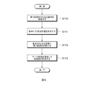
- FIG. 4 is a flowchart showing a method for manufacturing a crystal resonator according to the first embodiment of the present invention.
- FIG. 5 is a flowchart showing details of step S11 in FIG.
- FIG. 6 is a cross-sectional view of a crystal resonator according to a second embodiment of the present invention.
- FIG. 1 is an exploded perspective view of the crystal resonator according to the first embodiment of the present invention.
- 2 is a cross-sectional view taken along line II-II in FIG.
- FIG. 3 is a plan view of the base member of FIG.
- the crystal resonator 1 includes a crystal resonator element (Quartz Crystal Resonator) 10, a lid member 20, and a base member 30.
- the lid member 20 and the base member 30 are holders for housing the crystal resonator element 10.
- the lid member 20 has a concave shape
- the base member 30 has a flat plate shape.
- the crystal resonator element 10 has an AT-cut crystal piece (Quartz Crystal Blank) 11.
- the AT-cut crystal piece 11 is composed of an X-axis, a Y-axis, and a Z-axis which are crystal axes of an artificial quartz (Synthetic Quartz Crystal), and the Y-axis and the Z-axis from the Y-axis around the X-axis.
- XZ ′ surface When the axes rotated 35 degrees 15 minutes ⁇ 1 minute 30 seconds in the direction of the Z axis are respectively the Y ′ axis and the Z ′ axis, a plane parallel to the plane specified by the X axis and the Z ′ axis (hereinafter, “ It is called “XZ ′ surface.
- the crystal piece 11 has a first main surface 12a and a second main surface 12b which are XZ ′ surfaces facing each other.
- the crystal piece 11 which is an AT-cut crystal piece has a long side parallel to the X-axis direction, a short side parallel to the Z′-axis direction, and a side in the thickness direction parallel to the Y′-axis direction.
- the crystal piece 11 has a rectangular shape on the XZ ′ plane.
- a quartz resonator element using an AT-cut quartz piece has extremely high frequency stability over a wide temperature range, is excellent in aging characteristics, and can be manufactured at low cost. Further, the AT-cut quartz crystal resonator element uses a thickness shear vibration mode as a main vibration.
- the crystal piece 11 has a flat plate shape.
- Each of the first main surface 12a and the second main surface 12b has a flat surface.
- the crystal resonator element 10 includes a first excitation electrode 14a and a second excitation electrode 14b that constitute a pair of electrodes.
- the first excitation electrode 14a is provided on the first main surface 12a.
- the second excitation electrode 14b is provided on the second main surface 12b.
- the first excitation electrode 14a and the second excitation electrode 14b are provided to face each other across the crystal piece 11 in a region including the center of each main surface.
- the first excitation electrode 14a and the second excitation electrode 14b are arranged so as to substantially overlap each other on the XZ ′ plane.
- the first excitation electrode 14a and the second excitation electrode 14b each have a long side parallel to the X-axis direction, a short side parallel to the Z′-axis direction, and a thickness parallel to the Y′-axis direction. .
- the long sides of the first excitation electrode 14a and the second excitation electrode 14b are parallel to the long side of the crystal piece 11, and similarly, the first excitation electrode 14a and the second excitation electrode 14b.
- the short side of the excitation electrode 14 b is parallel to the short side of the crystal piece 11.
- the long sides of the first excitation electrode 14 a and the second excitation electrode 14 b are separated from the long side of the vibration part 17, and the short sides of the first excitation electrode 14 a and the second excitation electrode 14 b are from the short side of the vibration part 17. is seperated.
- the crystal resonator element 10 has extraction electrodes 15a and 15b and connection electrodes 16a and 16b.
- the connection electrode 16a is electrically connected to the first excitation electrode 14a via the extraction electrode 15a.
- the connection electrode 16b is electrically connected to the second excitation electrode 14b through the extraction electrode 15b.
- the connection electrode 16 a and the connection electrode 16 b are terminals for electrically connecting to the base member 30.
- the connection electrode 16 a and the connection electrode 16 b are provided on the second main surface 12 b of the crystal piece 11, and are arranged along the short side direction in the vicinity of the short side of the crystal piece 11 on the Z′-axis negative direction side.
- the extraction electrode 15a electrically connects the first excitation electrode 14a and the connection electrode 16a. Specifically, the extraction electrode 15a extends on the first main surface 12a from the first excitation electrode 14a in the Z′-axis negative direction and the X-axis negative direction, and from the first main surface 12a to the crystal piece 11. It extends so as to reach the second main surface 12b through each side surface, and is electrically connected to the connection electrode 16a on the second main surface 12b.
- the extraction electrode 15b electrically connects the second excitation electrode 14b and the electrode pad 16b.
- the extraction electrode 15b extends from the second excitation electrode 14b toward the Z′-axis negative direction and the X-axis positive direction on the second main surface 12b, and the connection electrode 16b on the second main surface 12b. And are electrically connected.
- the connection electrodes 16a and 16b electrically connected to the first excitation electrodes 14a and 14b provided on both main surfaces are connected to one of the second main surfaces 12b. Can be arranged.
- connection electrodes 16a and 16b are electrically connected to the electrode of the base member 30 through the conductive holding members 36a and 36b.
- the conductive holding members 36a and 36b are formed by thermally curing a conductive adhesive.
- the materials of the first excitation electrode 14a and the second excitation electrode 14b, the extraction electrodes 15a and 15b, and the electrode pads 16a and 16b are not particularly limited.
- a chromium (Cr) layer is used as a base.
- a gold (Au) layer may be further provided on the surface of the chromium layer.
- the lid member 20 is bonded to the base member 30, and thereby accommodates the crystal resonator element 10 in the internal space 26.
- the lid member 20 has an inner surface 24 and an outer surface 25 and has a concave shape opened toward the first main surface 32 a of the base member 30.
- the lid member 20 has a top surface portion 21 that faces the first main surface 32 a of the base member 30, and a side wall that is connected to the outer edge of the top surface portion 21 and extends in the normal direction with respect to the main surface of the top surface portion 21. Part 22.
- the lid member 20 has a rectangular shape when viewed from the normal direction of the main surface of the top surface portion 21.
- the lid member 20 includes, for example, a long side direction in which a long side parallel to the Z′-axis direction extends, a short side direction in which a short side parallel to the X-axis direction extends, and a height parallel to the Y′-axis direction.
- the lid member 20 has a facing surface 23 that faces the first main surface 32a of the base member 30 at the concave opening edge, and the facing surface 23 has a frame shape so as to surround the quartz vibrating element 10. It is extended.
- the material of the lid member 20 is not particularly limited, but is made of a conductive material such as metal. According to this, a shield function can be added by electrically connecting the lid member 20 to the ground potential.
- the lid member 20 is made of an alloy (for example, 42 alloy) containing iron (Fe) and nickel (Ni). Further, a gold (Au) layer for the purpose of preventing oxidation or the like may be provided on the outermost surface of the lid member 20.
- the lid member 20 may be an insulating material or a composite structure of a conductive material and an insulating material.
- the base member 30 supports the crystal resonator element 10 so that it can be excited. Specifically, the crystal resonator element 10 is held on the first main surface 32a of the base member 30 through the conductive holding members 36a and 36b so as to be able to be excited.
- the base member 30 has a flat plate shape.
- the base member 30 has a long side direction in which a long side parallel to the X-axis direction extends, a short side direction in which a short side parallel to the Z′-axis direction extends, and a thickness parallel to the Y′-axis direction. Extending in the thickness direction.
- the base member 30 has a base 31.
- the base 31 has a first main surface 32a and a second main surface 32b which are XZ ′ surfaces facing each other.
- the base 31 is a first sintered material such as an insulating ceramic (alumina). In this case, a plurality of insulating ceramic sheets may be laminated and sintered.
- the base 31 is made of a glass material (for example, silicate glass or a material mainly composed of materials other than silicate and having a glass transition phenomenon due to a temperature rise), a crystal material (for example, an AT-cut crystal), or You may form with a glass epoxy resin.
- the base 31 is preferably made of a heat resistant material.
- the substrate 31 may be a single layer or a plurality of layers. When the substrate 31 is a plurality of layers, the substrate 31 includes an insulating layer formed on the outermost layer of the first main surface 32a.
- the base member 30 includes electrode pads 33a and 33b provided on the first main surface 32a and external electrodes 35a, 35b, 35c and 35d provided on the second main surface.
- the electrode pads 33 a and 33 b are terminals for electrical connection with the crystal resonator element 10.
- the external electrodes 35a, 35b, 35c, and 35d are terminals for electrically connecting to a mounting board (not shown).
- the electrode pad 33a is electrically connected to the external electrode 35a via a via electrode 34a extending in the Y′-axis direction
- the electrode pad 33b is an external electrode via a via electrode 34b extending in the Y′-axis direction. It is electrically connected to 35b.
- the via electrodes 34a and 34b are formed in via holes that penetrate the base 31 in the Y′-axis direction.
- the electrode pads 33a and 33b are provided in the vicinity of the short side of the base member 30 on the negative X-axis side on the first main surface 32a, and are arranged away from the short side of the base member 30 and along the short side direction. ing.
- the electrode pad 33a is connected to the connection electrode 16a of the crystal resonator element 10 via the conductive holding member 36a
- the electrode pad 33b is connected to the connection electrode 16b of the crystal resonator element 10 via the conductive holding member 36b. Is done.
- the plurality of external electrodes 35a, 35b, 35c, and 35d are provided near the respective corners of the second main surface 32b.
- the external electrodes 35a and 35b are disposed immediately below the electrode pads 33a and 33b. Accordingly, the external electrodes 35a and 35b can be electrically connected to the electrode pads 33a and 33b by the via electrodes 34a and 34b extending in the Y′-axis direction.
- the external electrodes 35a and 35b arranged near the short side of the base member 30 on the negative X-axis side receive input / output signals of the crystal resonator element 10. Input / output electrodes to be supplied.
- the external electrodes 35c and 35d arranged near the short side of the base member 30 on the X axis positive direction side are dummy electrodes to which input / output signals of the crystal resonator element 10 are not supplied. Such dummy electrodes are not supplied with input / output signals of other electronic elements on a mounting board (not shown) on which the crystal unit 1 is mounted.
- the external electrodes 35c and 35d may be grounding electrodes to which a ground potential is supplied. As shown in FIG. 2, when the lid member 20 is made of a conductive material, the lid member 20 can be connected to the external electrode 35 c serving as ground electricity, thereby improving the shielding function of the lid member 20.
- a sealing frame 37 is provided on the first main surface 32 a of the base 31.
- the sealing frame 37 has a rectangular frame shape when viewed from the normal direction of the first main surface 32a.
- the electrode pads 33 a and 33 b are disposed inside the sealing frame 37.
- the sealing frame 37 is made of a conductive material.
- a joining member 40 described later is provided on the sealing frame 37, whereby the lid member 20 is joined to the base member 30 via the joining member 40 and the sealing frame 37.
- the base member 30 has protrusions 38 and 39 provided on the first main surface 32a of the base 31.
- the protrusions 38 and 39 are formed in a column shape extending in the normal direction of the first main surface 32 a of the base 31.
- the protrusions 38 and 39 have a tapered surface whose tip is smaller in diameter than the base end.
- the protrusions 38 and 39 may have the same diameter at the distal end and the proximal end.
- the protrusions 38 and 39 restrain the movement of the lid member 20 when the base member 30 is viewed in plan view from the normal direction of the first main surface 12a.
- the protrusions 38 and 39 are provided on the first main surface 32 in contact with the sealing frame 37.
- the protrusions 38 and 39 are made of a conductive material and are electrically connected to the sealing frame 37.
- the protrusions 38 and 39 are provided in the vicinity of two opposing corners of the sealing frame 37 on the first main surface 32a.
- the protrusions 38 and 39 are provided such that their outer edges protrude beyond the inner peripheral edge of the sealing frame 37 having a rectangular frame shape. ing.
- the protrusion 38 and the protrusion 39 are electrically connected to the external electrode 35c.
- the protruding portion 38 is electrically connected to the external electrode 35 c through the via electrode 43, the sealing frame 37, the bonding member 40, and the via electrode 44.
- the protrusion 38 is electrically connected to a via electrode 43 extending in the Y′-axis direction, and the via electrode 43 is connected to the first main surface 32 a in the intermediate layer of the base 31. It is also possible to electrically connect to the internal wiring 45 extending in the parallel direction.
- the via electrode 43 is formed by filling the concave portion 41 opened in the first main surface 32a with a conductive material.
- the protrusion 39 is electrically connected to the external electrode 35c with a via electrode 44 extending in the Y′-axis direction interposed.
- the via electrode 44 is formed by filling a hole 42 penetrating the base 31 from the first main surface 32a to the second main surface 32b with a conductive material.
- the external electrode 35d is a dummy electrode.
- the electrode pads 33a and 33b, the external electrodes 35a to 35d, the sealing frame 37, and the protrusions 38 and 39 of the base member 30 are all made of a metal film.
- the electrode pads 33a and 33b and the external electrodes 35a to 35d are configured by laminating a molybdenum (Mo) layer, a nickel (Ni) layer, and a gold (Au) layer from the lower layer to the upper layer.
- the sealing frame 37 and the protrusions 38 and 39 are configured by a molybdenum (Mo) layer.
- the sealing frame 37 and the protrusions 38 and 39 may be formed by laminating a gold (Au) layer on a molybdenum (Mo) layer.
- a molybdenum (Mo) layer may be formed by screen printing, and a gold (Au) layer may be formed by a plating method.
- Au gold
- the airtightness and the bonding strength can be further improved as will be described in the following examples.
- a nickel (Ni) layer may be interposed between the molybdenum (Mo) layer and the gold (Au) layer.
- the via electrodes 34a and 34b and the via electrodes 43 and 44 can be formed by filling the via holes or the recesses of the base 21 with a metal material such as molybdenum.
- the protrusion 38 is provided on the via electrode 43, and the protrusion 39 is provided on the via electrode 44.
- the protrusions 38 and 39 and the via electrodes 43 and 44 are made of the same conductive material such as molybdenum.
- the protrusions 38 and 39 and the via electrodes 43 and 44 are made of a second sintered material having a smaller sintering shrinkage rate than the first sintered material of the base 31. According to this, when the base member 30 is sintered, at least the upper surfaces of the via electrodes 43 and 44 are raised and protrude from the first main surface 32a due to the difference in sintering shrinkage ratio between the two. 38 and 39 can be formed easily.
- the positional relationship between the electrode pads 33a and 33b and the external electrodes 35a to 35d is not limited to the above example.
- the electrode pad 33 a may be disposed near one short side of the base member 30, and the electrode pad 33 b may be disposed near the other short side of the base member 30.
- the crystal resonator element 10 is held by the base member 30 at each short side end of the crystal piece 11.
- the arrangement of the external electrodes is not limited to the above example.
- two input / output electrodes may be provided on the diagonal of the second main surface 32b.
- the four external electrodes may be arranged near the center of each side instead of the corner of the second main surface 32b.
- the number of external electrodes is not limited to four, and may be, for example, only two that are input / output electrodes.
- the manner of electrical connection between the electrode pad and the external electrode is not limited to the via electrode, and the electrical connection between the electrode pads and the external electrodes by arranging the surface wiring on the first main surface 32a or the second main surface 32b. May be achieved.
- the base 31 of the base member 30 is formed of a plurality of layers, the via electrode extends to reach the intermediate layer, and the internal wiring is arranged in the intermediate layer to achieve electrical connection between the electrode pad and the external electrode. May be.
- the crystal vibrating element 10 is surrounded by the lid member 20 and the base member 30 by joining both the lid member 20 and the base member 30 via the sealing frame 37 and the joining member 40.
- the inner space (cavity) 26 is sealed.
- the pressure in the internal space is preferably in a vacuum state lower than the atmospheric pressure, and this is preferable because changes over time due to oxidation of the first excitation electrode 14a and the second excitation electrode 14b can be reduced.
- the joining member 40 is provided over the entire circumference of the lid member 20 and the base member 30. Specifically, the joining member 40 is provided on the sealing frame 37 and the protrusions 38 and 39. The joining member 40 is provided so as to cover the protrusions 38 and 39.
- the crystal resonator element 10 is connected to the lid member 20 and the base. Sealed by the member 30. At this time, portions of the joining member 40 that cover the protrusions 38 and 39 abut against the side wall portion 22 of the lid member 20. Thus, the movement of the lid member 20 can be restricted by the protrusions 38 and 39.
- the joining member 40 is, for example, a brazing member. Specifically, the joining member 40 is made of a gold (Au) -tin (Sn) eutectic alloy. Thus, the lid member 20 and the base member 30 are metal-bonded. According to the metal bonding, the sealing performance can be improved.
- the bonding member 40 may be formed of one material layer such as a brazing member (for example, gold (Au) -tin (Sn) eutectic alloy), but may be formed of two or more material layers. Good.
- a brazing member for example, gold (Au) -tin (Sn) eutectic alloy
- the bonding member 40 is not limited to a conductive material, and may be an insulating material such as a glass adhesive material such as low-melting glass (for example, lead borate or tin phosphate) or a resin adhesive. According to this, the cost is lower than that of metal bonding, the heating temperature can be suppressed, and the manufacturing process can be simplified.
- a glass adhesive material such as low-melting glass (for example, lead borate or tin phosphate) or a resin adhesive.
- the portion covering the protrusions 38 and 39 in the joining member 40 is in contact with the side wall portion 22 on the inner surface 24 side of the lid member 20. Accordingly, the movement of the lid member 20 can be easily and effectively restricted by the protrusions 38 and 39.
- one end of the crystal piece 11 in the long side direction (the end on the side where the conductive holding members 36a and 36b are disposed) is a fixed end, and the other end is a free end. It has become.
- the crystal resonator element 10, the lid member 20, and the base member 30 each have a rectangular shape on the XZ ′ plane, and the long side direction and the short side direction are the same.
- the position of the fixed end of the crystal resonator element 10 is not particularly limited, and as a modification, the crystal resonator element 10 may be fixed to the base member 30 at both ends of the crystal piece 11 in the long side direction.
- the crystal resonator element 10 and the electrodes of the base member 30 may be formed in such a manner that the crystal resonator element 10 is fixed at both ends of the crystal piece 11 in the long side direction.
- an alternating electric field is applied between the pair of first and second excitation electrodes 14 a and 14 b in the crystal resonator element 10 via the external electrodes 35 a and 35 b of the base member 30. .
- the vibration part 17 of the crystal piece 11 vibrates by a predetermined vibration mode such as a thickness shear vibration mode, and resonance characteristics associated with the vibration are obtained.
- the portion of the joining member 40 that covers the protrusions 38 and 39 restrains the movement of the lid member 20 when viewed in plan from the normal direction of the first main surface 32a of the base member 30. In contact with the side wall 22 of the lid member 20. According to this, since the joining member 40 that covers the protrusions 18 and 19 comes into contact with the side wall portion 22 of the lid member 20, the joining strength can be improved. Furthermore, since it can suppress that the position shift of the cover member 20 occurs, the airtightness of the crystal resonator element 10 can be improved.
- FIG. 4 is a flowchart showing a method of manufacturing the crystal unit 1
- FIG. 5 is a flowchart for explaining details of the step (S11) of preparing the base member 30 in FIG.
- the crystal resonator element 10 is prepared (S10). Since the crystal piece processing step and the various electrode forming steps are common, the description thereof is omitted. The configuration of the crystal resonator element 10 is as already described.
- the base member 30 is prepared (S11). Specifically, as shown in FIG. 5, a base 31 made of the first sintered material is prepared (S110).
- the first sintered material is an insulating ceramic such as alumina.
- a recess 41 and a hole 42 are formed in the base 31 by etching or the like (S111), and a second sintered material is provided in the recess 41 and the hole 42 (S112).
- a second sintered material for example, a molybdenum material can be provided by a screen printing method.
- the second sintered material can be filled in the recesses 41 and the holes 42 by applying the second sintered material onto the base 31 and leveling it flat with a squeegee.
- the base member 30 is sintered to form the protrusions 38 and 39 (S113).
- the first sintered material that is the base 31 has a smaller sintering shrinkage rate than the second sintered material provided in the recess 41 and the hole 42, so that the second sintering is performed by performing the sintering process.
- the material bulges from the inside of the opening of the recess 41 and the hole 42 to the outside.
- the upper surface of the via electrode 43 is raised by the second sintered material provided in the recessed portion 41, and the protruding portion 38 protruding on the via electrode 43 is formed.
- the upper surface of the via electrode 44 is raised by the second sintered material provided in the hole 42, and a protrusion 39 that protrudes on the via electrode 44 is formed.
- various electrodes including the electrode pads 33a and 33b, the via electrodes 34a and 34b, the external electrodes 35a to 35d, the sealing frame 37, and the like can be formed.
- the base member 30 shown in FIG. 1 can be prepared.
- the crystal resonator element 10 is mounted on the first main surface 32a of the base 31 of the base member 30 (S12). Specifically, a conductive adhesive is applied on the electrode pads 33a and 33b on the first main surface 32a of the base 31, and the conductive adhesive is thermally cured in a state where the crystal resonator element 10 is mounted.
- the connection electrodes 16a and 16b of the crystal resonator element 10 and the connection electrodes 33a and 33b of the base member 30 are electrically connected by the conductive holding members 36a and 36b in which the conductive adhesive is thermally cured.
- the quartz crystal vibration element 70 can be held excitable by the conductive holding members 36a and 36b.
- the crystal resonator element 10 is mounted on the first main surface 32a so that the second excitation electrode 14b faces the base member 30 side.
- the lid member 20 is joined to the base member 30 via the joining member 40 (S13).
- the portion of the joining member 40 that covers the protrusions 38 and 39 is brought into contact with the side wall portion 22 of the lid member 20.
- the joining member 40 may be provided on the sealing frame 37 and the protruding portions 38 and 39 so as to cover them, and then the lid member 20 may be joined to the base member 30.
- Example 1 In the crystal resonator according to the following manufacturing conditions, when the bonding strength was measured for the sample A with protrusions according to the present embodiment and the sample B without protrusions according to the comparative example, the sample A with protrusions was as follows. It was found that the bonding strength was excellent.
- Conditions common to samples A and B are as follows. That is, a hermetically sealed crystal resonator having an outer dimension (long side direction ⁇ short side direction) of 1.2 mm ⁇ 1.0 mm, which is made of alumina and 0.125 mm thick on which the crystal piece is placed. A base member and a lid member that is a concave metal cap are provided. The joining member was an AuSn alloy, and the rectangular sealing frame was formed with a width of 0.1 mm in order to obtain an airtight sealing structure.
- the external dimensions (long side direction ⁇ short side direction ⁇ height) of the concave metal cap are 1.2 mm ⁇ 1.0 mm ⁇ 0.16 mm, and the thickness of the top surface portion 21 and the side wall portion 22 is as follows. It was formed at 0.06 mm.
- the sealing frame and the protrusion were subjected to a heat treatment at 320 ° C. together with the joining member, whereby the lid member was fused to the base member.
- protrusions formed by raising ⁇ 0.06 mm via electrodes (molybdenum) formed in the base member at two diagonal positions of the sealing frame were formed.
- the height of the protrusion is 0.01 mm higher than the height of the sealing frame 0.02 mm.
- the protrusions were made of molybdenum (Mo), which is the same material as the sealing frame and via electrodes.
- Test method It was measured by “Test Ue3: Adhesion (shear strength) test” defined by “JIS C 60068-2-21 (2009)”.
- Example 2 In the crystal resonator element according to the following manufacturing conditions, the bonding strength and the leak test were performed on the sample C of the example according to this embodiment and the sample D of another example according to this embodiment. It was found that the method is superior in bonding strength and leak test.
- Conditions common to samples C and D are as follows. That is, a hermetically sealed crystal resonator having an outer dimension (long side direction ⁇ short side direction) of 1.2 mm ⁇ 1.0 mm, which is made of alumina and 0.125 mm thick on which the crystal piece is placed. A base member and a lid member that is a concave metal cap are provided.
- the rectangular sealing frame was formed with a width of 0.1 mm in order to obtain an airtight sealing structure.
- the external dimensions (long side direction ⁇ short side direction ⁇ height) of the concave metal cap are 1.2 mm ⁇ 1.0 mm ⁇ 0.16 mm, and the top and side portions of the concave metal cap Was formed with a thickness of 0.06 mm.
- the sealing frame and the protruding portion were subjected to a heat treatment at 320 ° C. together with the bonding member made of AuSn alloy, thereby fusing the lid member to the base member.
- sample C protrusions formed by raising ⁇ 0.06 mm via electrodes (Mo) formed in the base member at two diagonal positions of the sealing frame were formed.
- a sealing frame made of molybdenum was formed avoiding the tip (head) of the protrusion, and an Au plating layer of 0.2 ⁇ m was formed in a region including the tip of the protrusion.
- the Au plating layer was integrally formed on the tip of the protrusion and the sealing frame.
- an AuSn alloy was formed on the protrusion and the sealing frame.
- sample D an alumina piece made of the same material as the base member was laminated on the surface of the base member to form a protrusion.
- a sealing frame made of molybdenum was formed avoiding the tip (head) of the protrusion.
- an AuSn alloy jointing member was formed on the protrusion and the sealing frame.
- Sample C Mo
- Sample D alumina
- the sample C can suppress generation
- the tip of the protruding portion exposed from the sealing frame is covered with an Au plating layer, and this is continuous with the Au plating layer on the sealing frame. It is considered that the occurrence of defective products can be suppressed.
- FIG. 6 is a cross-sectional view of the crystal unit 2 according to the present embodiment.
- FIG. 6 is a drawing in the same cross-sectional view as FIG.
- symbol is attached
- differences from the first embodiment will be described.
- the crystal resonator 2 includes a base member 130, and the configuration of the base member 130 is different from that of the first embodiment.
- the base member 130 has projections 138 and 139 and a joining member 140, and a portion of the joining member 140 that covers the projections 138 and 139 is on the outer surface 25 side of the lid member 20. It is in contact with the side wall 22.
- the projecting portions 138 and 139 are provided so that their outer edges protrude outside the outer peripheral edge of the sealing frame 137 having a rectangular frame shape. It has been.
- the protrusion 138 is provided on the via electrode 43 formed in the recess 141 of the base 131, and the protrusion 139 is on the via electrode 144 formed in the hole 142 of the base 131. Is provided.
- the movement of the lid member 20 can be restrained from the outer surface 25 side of the lid member 20 by the portion covering the protrusions 138 and 139 in the joining member 140. Therefore, also in this embodiment, it is possible to improve positioning accuracy, bonding strength, and airtightness.
- the present invention is not limited to the above-described embodiment, and can be variously modified and applied.
- protrusions there are two protrusions.
- two or more protrusions are sufficient.
- three protrusions may be provided to support three corners of the four corners of the rectangular lid member, and four protrusions may be provided to support the four corners of the rectangular lid member.
- the protrusion is not limited to be formed on the via electrode, and the via electrode may not be formed immediately below the protrusion.
- the method for forming the protrusions is not limited to the formation method based on the difference in sintering shrinkage, and the protrusions may be formed by, for example, laminating material pieces on the base member.
- the present invention is not limited to this, and a mesa structure in which the vibration part including the center of the main surface is thicker than the peripheral part is provided. You may employ
- the quartz resonator element extends from the base and the base using a quartz plate cut out at a predetermined angle with respect to the X axis, the Y axis, and the Z axis orthogonal to each other as crystal axes of the quartz. It may be a tuning fork type crystal vibrating element including a crystal piece having at least one vibrating arm and an excitation electrode provided on the vibrating arm so as to bend and vibrate.
- a different cut (for example, BT cut) other than the AT cut may be applied to the cut angle of the crystal piece.
- each embodiment described above is for facilitating understanding of the present invention, and is not intended to limit the present invention.
- the present invention can be changed / improved without departing from the spirit thereof, and the present invention includes equivalents thereof.
- those obtained by appropriately modifying the design of each embodiment by those skilled in the art are also included in the scope of the present invention as long as they include the features of the present invention.
- each element included in each embodiment and its arrangement, material, condition, shape, size, and the like are not limited to those illustrated, and can be changed as appropriate.
- each element included in each embodiment can be combined as much as technically possible, and combinations thereof are included in the scope of the present invention as long as they include the features of the present invention.
Abstract
水晶片(11)と、水晶片(11)の両主面(12a,12b)に互いに対向するように設けられた一対の励振電極(14a,14b)と、励振電極(14a,14b)に電気的に接続された接続電極(16a,16b)とを有する水晶振動素子(10)と、水晶振動素子(10)が表面に搭載されたベース部材(30)と、ベース部材(30)の表面(32a)に接合部材(40)を介して接合され、水晶振動素子(10)をベース部材(30)の表面(32a)上で内部空間(26)に収容する蓋部材(20)とを備え、接合部材(40)における突起部(38,39)を覆う部分が、ベース部材(30)の表面(12a)の法線方向から平面視したときに、蓋部材(20)の動きを拘束するように蓋部材(20)の側壁部(22)に当接されている。
Description
本発明は、水晶振動子及びその製造方法に関する。本発明は特に、水晶振動素子と、ベース部材と、蓋部材とを備える水晶振動素子及びその製造方法に関する。
発振装置や帯域フィルタなどに用いられる基準信号の信号源に水晶振動子が広く用いられている。水晶振動子は、例えば、水晶振動素子と、水晶振動素子が搭載されたベース部材と、水晶振動素子を内部空間に収容するようにベース部材に接合される蓋部材とを備える。この場合、蓋部材の接合位置の精度が悪いと気密性が損なわれ、水晶振動子の所望の周波数が得られなくなる場合がある。そこで、例えば特許文献1では、凹状カバーに突起を形成し、これを平板ベースに形成した穴に位置合わせする構成が開示されている。また、特許文献2では、金属カバー体の内壁に当たる位置にセラミックベース板に突起部を形成する構成が開示されている。
しかしながら、特許文献1の構成では、穴と突起の位置精度が良くないと気密性を損なう可能性がある。また、特許文献2の構成においても、セミタックベース板の表面の法線方向から平面視したときに、突起部が凹状カバーの内壁に直接的に当たることによって位置合わせするため、突起部の形成位置の精度が良くないと気密性を損なう可能性がある。また、特許文献2では、突起部を金属カバー体の封止部を避けて設ける必要があるため、突起部の加工精度が要求される場合がある。
本発明はこのような事情に鑑みてなされたものであり、水晶振動素子の気密性を向上させるとともに蓋部材とベース部材との間の接合強度の向上が図れる水晶振動子及びその製造方法を提供することを目的とする。
本発明の一側面に係る水晶振動子は、水晶片と、水晶片を挟んで対向するように水晶片の両主面に設けられた一対の励振電極と、一対の励振電極のそれぞれに電気的に接続された一対の接続電極とを有する水晶振動素子と、水晶振動素子が表面に搭載されたベース部材と、ベース部材の表面に接合部材を介して接合され、水晶振動素子をベース部材の表面上で内部空間に収容する蓋部材とを備え、ベース部材は、表面上に2つ以上の突起部を有し、接合部材は、少なくとも突起部を覆うようにベース部材の表面上に設けられ、蓋部材は、ベース部材の表面に向かって延在する側壁部を有し、接合部材における突起部を覆う部分が、ベース部材の表面の法線方向から平面視したときに、蓋部材の動きを拘束するように蓋部材の側壁部に当接されている。
上記構成によれば、突起部を覆う接合部材が蓋部材の側壁部に当接するため、接合強度の向上を図ることができる。さらに、蓋部材の位置ずれが発生することを抑制することができるため、水晶振動素子の気密性の向上を図ることができる。
本発明の他の一側面に係る水晶振動子の製造方法は、水晶片と、水晶片を挟んで対向するように水晶片の両主面に設けられた一対の励振電極と、励振電極に電気的に接続された一対の接続電極とを有する水晶振動素子を準備する工程と、ベース部材を準備する工程と、水晶振動素子をベース部材の表面に搭載する工程と、水晶振動素子をベース部材の表面上で内部空間に収容するように、蓋部材を接合部材を介してベース部材の表面に接合する工程とを含み、ベース部材は、表面上に2つ以上の突起部を有し、接合部材は、少なくとも突起部を覆うようにベース部材の表面上に設けられ、蓋部材は、ベース部材の表面に向かって延在する側壁部を有し、蓋部材を接合する工程において、接合部材における突起部を覆う部分を、ベース部材の表面の法線方向から平面視したときに、蓋部材の動きを拘束するように蓋部材の側壁部に当接させる。
上記構成によれば、突起部を覆う接合部材を蓋部材の側壁部に当接させるため、接合強度の向上を図ることができる。さらに、蓋部材の位置ずれが発生することを抑制することができるため、水晶振動素子の気密性の向上を図ることができる。
本発明によれば、水晶振動素子の気密性を向上させるとともに蓋部材とベース部材との間の接合強度の向上が図れる水晶振動子及びその製造方法を提供することを目的とする。
以下に本発明の実施形態を説明する。以下の図面の記載において、同一又は類似の構成要素は同一又は類似の符号で表している。図面は例示であり、各部の寸法や形状は模式的なものであり、本願発明の技術的範囲を当該実施形態に限定して解するべきではない。
<第1実施形態>
図1~図3を参照しつつ、本発明の第1実施形態に係る水晶振動子(Quartz Crystal Resonator Unit)について説明する。ここで、図1は、本発明の第1実施形態に係る水晶振動子の分解斜視図である。図2は、図1のII-II線断面図である。図3は、図1のベース部材の平面図である。
図1~図3を参照しつつ、本発明の第1実施形態に係る水晶振動子(Quartz Crystal Resonator Unit)について説明する。ここで、図1は、本発明の第1実施形態に係る水晶振動子の分解斜視図である。図2は、図1のII-II線断面図である。図3は、図1のベース部材の平面図である。
図1に示すように、本実施形態に係る水晶振動子1は、水晶振動素子(Quartz Crystal Resonator)10と、蓋部材20と、ベース部材30とを備える。蓋部材20及びベース部材30は、水晶振動素子10を収容するための保持器である。図1に示す例では、蓋部材20は凹状をなしており、ベース部材30は平板状をなしている。
水晶振動素子10は、ATカット型の水晶片(Quartz Crystal Blank)11を有する。ATカット型の水晶片11は、人工水晶(Synthetic Quartz Crystal)の結晶軸(Crystallographic Axes)であるX軸、Y軸、Z軸のうち、Y軸及びZ軸をX軸の周りにY軸からZ軸の方向に35度15分±1分30秒回転させた軸をそれぞれY´軸及びZ´軸とした場合、X軸及びZ´軸によって特定される面と平行な面(以下、「XZ´面」と呼ぶ。他の軸によって特定される面についても同様である。)を主面として切り出されたものである。水晶片11は、互いに対向するXZ´面である第1主面12a及び第2主面12bを有する。
ATカット水晶片である水晶片11は、X軸方向に平行な長辺と、Z´軸方向に平行な短辺と、Y´軸方向に平行な厚さ方向の辺とを有する。また、水晶片11は、XZ´面において矩形状をなしている。
ATカット水晶片を用いた水晶振動素子は、広い温度範囲で極めて高い周波数安定性を有し、また、経時変化特性にも優れている上、低コストで製造することが可能である。また、ATカット水晶振動素子は、厚みすべり振動モード(Thickness Shear Vibration Mode)を主振動として用いられる。
本実施形態では、水晶片11は平板な板状をなしている。第1主面12a及び第2主面12bはそれぞれ平坦面を有する。
水晶振動素子10は、一対の電極を構成する第1励振電極14a及び第2励振電極14bを有する。第1励振電極14aは、第1主面12aに設けられている。また、第2励振電極14bは、第2主面12bに設けられている。第1励振電極14aと第2励振電極14bは、各主面の中央を含む領域で水晶片11を挟んで互いに対向して設けられている。第1励振電極14aと第2励振電極14bは、XZ´面において略全体が重なり合うように配置されている。
第1励振電極14a及び第2励振電極14bは、それぞれ、X軸方向に平行な長辺と、Z´軸方向に平行な短辺と、Y´軸方向に平行な厚さとを有している。図1に示す例では、XZ´面において、第1励振電極14a及び第2励振電極14bの長辺は、水晶片11の長辺と平行であり、同様に、第1励振電極14a及び第2励振電極14bの短辺は、水晶片11の短辺と平行である。また、第1励振電極14a及び第2励振電極14bの長辺は振動部17の長辺から離れており、第1励振電極14a及び第2励振電極14bの短辺は振動部17の短辺から離れている。
水晶振動素子10は、引出電極15a,15bと、接続電極16a,16bとを有する。接続電極16aは、引出電極15aを介して第1励振電極14aと電気的に接続されている。また、接続電極16bは、引出電極15bを介して第2励振電極14bと電気的に接続されている。接続電極16a及び接続電極16bは、ベース部材30に電気的に接続するための端子である。接続電極16a及び接続電極16bは、水晶片11の第2主面12bに設けられ、水晶片11のZ´軸負方向側の短辺付近において当該短辺方向に沿って配列されている。
引出電極15aは、第1励振電極14aと接続電極16aとを電気的に接続している。具体的には、引出電極15aは、第1主面12a上において第1励振電極14aからZ´軸負方向及びX軸負方向に向かって延在し、第1主面12aから水晶片11の各側面を通って第2主面12bに至るように延在し、第2主面12b上の接続電極16aと電気的に接続されている。また、引出電極15bは、第2励振電極14bと電極パッド16bとを電気的に接続する。具体的には、引出電極15bは、第2主面12b上において第2励振電極14bからZ´軸負方向及びX軸正方向に向かって延在し、第2主面12b上の接続電極16bと電気的に接続されている。このように引出電極15a,15bを延在させることによって、両主面に設けられた第1励振電極14a,14bと電気的に接続された接続電極16a,16bを片方の第2主面12b上に配置させることができる。
接続電極16a,16bは、導電性保持部材36a,36bを介してベース部材30の電極に電気的に接続される。導電性保持部材36a,36bは、導電性接着剤が熱硬化して形成されたものである。
第1励振電極14a及び第2励振電極14b、引出電極15a,15b、並びに、電極パッド16a,16bの各電極の材料は特に限定されるものではないが、例えば、下地としてクロム(Cr)層を有し、クロム層の表面にさらに金(Au)層を有していてもよい。
蓋部材20は、ベース部材30に接合され、これによって水晶振動素子10を内部空間26に収容する。蓋部材20は、内面24及び外面25を有し、ベース部材30の第1主面32aに向かって開口した凹状をなしている。
蓋部材20は、ベース部材30の第1主面32aに対向する天面部21と、天面部21の外縁に接続されておりかつ天面部21の主面に対して法線方向に延在する側壁部22とを有する。蓋部材20は、天面部21の主面の法線方向から平面視したときに矩形状をなしている。蓋部材20は、例えば、Z´軸方向に平行な長辺が延在する長辺方向と、X軸方向に平行な短辺が延在する短辺方向と、Y´軸方向に平行な高さ方向とを有する。また、蓋部材20は、凹状の開口縁においてベース部材30の第1主面32aに対向する対向面23を有し、この対向面23は、水晶振動素子10の周囲を囲むように枠状に延在している。
蓋部材20の材質は特に限定されるものではないが、例えば金属などの導電材料で構成される。これによれば、蓋部材20を接地電位に電気的に接続させることによりシールド機能を付加することができる。例えば、蓋部材20は、鉄(Fe)及びニッケル(Ni)を含む合金(例えば42アロイ)からなる。また、蓋部材20の最表面に酸化防止等を目的とした金(Au)層などが設けられてもよい。あるいは、蓋部材20は、絶縁材料又は導電材料・絶縁材料の複合構造であってもよい。
ベース部材30は水晶振動素子10を励振可能に支持するものである。具体的には、水晶振動素子10は導電性保持部材36a,36bを介してベース部材30の第1主面32aに励振可能に保持されている。
ベース部材30は平板な板状をなしている。ベース部材30は、X軸方向に平行な長辺が延在する長辺方向と、Z´軸方向に平行な短辺が延在する短辺方向と、Y´軸方向に平行な厚さが延在する厚さ方向とを有する。
ベース部材30は基体31を有する。基体31は、互いに対向するXZ´面である第1主面32a及び第2主面32bを有する。基体31は、例えば絶縁性セラミック(アルミナ)などの第1焼結材である。この場合、複数の絶縁性セラミックシートを積層して焼結してもよい。あるいは、基体31は、ガラス材料(例えばケイ酸塩ガラス、又はケイ酸塩以外を主成分とする材料であって、昇温によりガラス転移現象を有する材料)、水晶材料(例えばATカット水晶)又はガラスエポキシ樹脂などで形成してもよい。基体31は耐熱性材料から構成されることが好ましい。基体31は、単層であっても複数層であってもよく、複数層である場合、第1主面32aの最表層に形成された絶縁層を含む。
ベース部材30は、第1主面32aに設けられた電極パッド33a,33bと、第2主面に設けられた外部電極35a,35b,35c,35dとを有する。電極パッド33a,33bは、水晶振動素子10と電気的に接続するための端子である。また、外部電極35a,35b,35c,35dは、図示しない実装基板と電気的に接続するための端子である。電極パッド33aは、Y´軸方向に延在するビア電極34aを介して外部電極35aに電気的に接続され、電極パッド33bは、Y´軸方向に延在するビア電極34bを介して外部電極35bに電気的に接続されている。ビア電極34a,34bは基体31をY´軸方向に貫通するビアホール内に形成される。
電極パッド33a,33bは、第1主面32a上においてベース部材30のX軸負方向側の短辺付近に設けられ、ベース部材30の短辺から離れてかつ当該短辺方向に沿って配列されている。電極パッド33aは、導電性保持部材36aを介して水晶振動素子10の接続電極16aが接続され、他方、電極パッド33bは、導電性保持部材36bを介して水晶振動素子10の接続電極16bが接続される。
複数の外部電極35a,35b,35c,35dは、第2主面32bのそれぞれの角付近に設けられている。図1に示す例では、外部電極35a,35bが、電極パッド33a,33bの直下に配置されている。これによってY´軸方向に延在するビア電極34a,34bによって、外部電極35a,35bを電極パッド33a,33bに電気的に接続することができる。図1に示す例では、4つの外部電極35a~dのうち、ベース部材30のX軸負方向側の短辺付近に配置された外部電極35a,35bは、水晶振動素子10の入出力信号が供給される入出力電極である。また、ベース部材30のX軸正方向側の短辺付近に配置された外部電極35c,35dは、水晶振動素子10の入出力信号が供給されないダミー電極となっている。このようなダミー電極には、水晶振動子1が実装される図示しない実装基板上の他の電子素子の入出力信号も供給されない。あるいは、外部電極35c,35dは、接地電位が供給される接地用電極であってもよい。図2で示すように、蓋部材20が導電性材料からなる場合、蓋部材20が接地電気となる外部電極35cに接続されることによって、蓋部材20にシールド機能の向上を図ることができる。
基体31の第1主面32aには、封止枠37が設けられている。封止枠37は、第1主面32aの法線方向から平面視したときに矩形の枠状をなしている。電極パッド33a,33bは、封止枠37の内側に配置されている。封止枠37は、導電材料により構成されている。封止枠37上には後述する接合部材40が設けられ、これによって蓋部材20が接合部材40及び封止枠37を介してベース部材30に接合される。
本実施形態に係るベース部材30は、基体31の第1主面32a上に設けられた突起部38,39を有する。突起部38,39は、基体31の第1主面32aの法線方向に延在する柱状に形成されている。例えば、突起部38,39は、先端が基端よりも径が小さいテーパ面を有している。あるいは、突起部38,39は、先端と基端が同じ径を有していてもよい。突起部38,39は、第1主面12aの法線方向からベース部材30を平面視したときに蓋部材20の動きを拘束するものである。
突起部38,39は、第1主面32上において、封止枠37に接触して設けられている。突起部38,39は導電材料により構成され、封止枠37と電気的に接続されている。図3に示す例では、突起部38,39は、第1主面32a上の封止枠37における対向する2つの角付近に設けられている。また、第1主面32aの法線方向から平面視したときに、突起部38,39はそれらの外縁が矩形の枠状をなす封止枠37の内周縁よりも内側にはみ出るように設けられている。突起部38,39を封止枠37の対向する2つの角付近に設けることによって、突起部38,39によって蓋部材20の対向する2つの角を支持することができる。
突起部38および突起部39は外部電極35cに電気的に接続されている。図3に示す例では、突起部38は、ビア電極43、封止枠37、接合部材40及びビア電極44を通して、外部電極35cに電気的に接続されている。あるいは、図3に示すように、突起部38は、Y´軸方向に延在するビア電極43に電気的に接続され、ビア電極43は、基体31の中間層において、第1主面32aと平行な方向に延在する内部配線45に電気的に接続することもできる。ビア電極43は、第1主面32aに開口する凹部41に導電材料を充填することによって形成される。また、突起部39は、Y´軸方向に延在するビア電極44を介在させて外部電極35cに電気的に接続されている。ビア電極44は、基体31を第1主面32aから第2主面32bに貫通する孔42に導電材料を充填することによって形成される。外部電極35dは、ダミー電極である。
ベース部材30の電極パッド33a,33b、外部電極35a~d、封止枠37及び突起部38,39はいずれも金属膜から構成されている。例えば、電極パッド33a,33b、外部電極35a~dは、下層から上層にかけて、モリブデン(Mo)層、ニッケル(Ni)層及び金(Au)層が積層されて構成されている。また、封止枠37及び突起部38,39は、モリブデン(Mo)層によって構成されている。あるいは、封止枠37及び突起部38,39は、モリブデン(Mo)層の上に金(Au)層を積層することによって形成してもよい。この場合、モリブデン(Mo)層をスクリーン印刷で形成し、金(Au)層をめっき法によって形成してもよい。金(Au)層を設けることによって後述の実施例で説明するように気密性及び接合強度のさらなる向上を図ることができる。なお、モリブデン(Mo)層と金(Au)層の間にニッケル(Ni)層を介在させてもよい。また、ビア電極34a,34b及びビア電極43,44は、基体21のビアホール又は凹部にモリブデンなどの金属材料を充填して形成することができる。
突起部38はビア電極43上に設けられ、突起部39はビア電極44上に設けられている。突起部38,39及びビア電極43,44は、例えばモリブデンなどの同一導電材料により構成されている。例えば、突起部38,39及びビア電極43,44を、基体31の第1焼結材よりも焼結収縮率が小さい第2焼結材から構成されている。これによれば、ベース部材30を焼結することにより、両者の焼結収縮率の違いに起因して、少なくともビア電極43,44の上面が隆起して第1主面32aから突起する突起部38,39を容易に形成することができる。
なお、電極パッド33a,33bや外部電極35a~35dの配置関係は上記例に限定されるものではない。例えば、電極パッド33aがベース部材30の一方の短辺付近に配置され、電極パッド33bがベース部材30の他方の短辺付近に配置されてもよい。このような構成においては、水晶振動素子10が、水晶片11のそれぞれの短辺側の端部においてベース部材30に保持されることになる。
また、外部電極の配置は上記例に限るものではなく、例えば、入出力電極である2つが第2主面32bの対角上に設けられていてもよい。あるいは、4つの外部電極は、第2主面32bの角ではなく各辺の中央付近に配置されていてもよい。また、外部電極の個数は4つに限るものではなく、例えば入出力電極である2つのみであってもよい。また、電極パッドと外部電極との電気的な接続の態様はビア電極によるものに限らず、第1主面32a又は第2主面32b上に表面配線を配置することによってそれらの電気的な導通を達成してもよい。あるいは、ベース部材30の基体31を複数層で形成し、ビア電極を中間層に至るまで延在させ、中間層において内部配線を配置することによって電極パッドと外部電極との電気的な接続を図ってもよい。
図2に示すように、蓋部材20及びベース部材30の両者が封止枠37及び接合部材40を介して接合されることによって、水晶振動素子10が、蓋部材20とベース部材30とによって囲まれた内部空間(キャビティ)26に封止される。この場合、内部空間の圧力は大気圧力よりも低圧な真空状態であることが好ましく、これにより第1励振電極14a,第2励振電極14bの酸化による経時変化などが低減できるため好ましい。
接合部材40は、蓋部材20及びベース部材30の各全周に亘って設けられている。具体的には、接合部材40は、封止枠37及び突起部38,39上に設けられている。接合部材40は、突起部38,39を覆って設けられている。
封止枠37及び接合部材40が、蓋部材20の側壁部22の対向面23とベース部材30の第1主面32aとの間に介在することによって、水晶振動素子10が蓋部材20及びベース部材30によって封止される。このとき、接合部材40における突起部38,39を覆う部分は、蓋部材20の側壁部22に当接する。こうして、突起部38,39によって蓋部材20における動きを拘束することができる。
接合部材40は、例えばろう部材である。具体的には、接合部材40は、金(Au)‐錫(Sn)共晶合金からなる。こうして、蓋部材20とベース部材30とを金属接合とする。金属接合によれば封止性を向上させることができる。
また、接合部材40は、ろう部材(例えば金(Au)‐錫(Sn)共晶合金)などの1つの材料層によって形成されていてもよいが、2以上の材料層によって形成されていてもよい。
なお、接合部材40は、導電材料に限らず、例えば低融点ガラス(例えば鉛ホウ酸系や錫リン酸系等)などのガラス接着材料又は樹脂接着剤などの絶縁性材料であってもよい。これによれば、金属接合に比べて低コストであり、また加熱温度を抑えることができ、製造プロセスの簡易化を図ることができる。
図2に示す例では、接合部材40における突起部38,39を覆う部分は、蓋部材20の内面24側において側壁部22に当接されている。これによって、突起部38,39によって容易かつ効果的に蓋部材20の動きを拘束することができる。
本実施形態に係る水晶振動素子10は、水晶片11の長辺方向の一方端(導電性保持部材36a,36bが配置される側の端部)が固定端であり、その他方端が自由端となっている。また、水晶振動素子10、蓋部材20及びベース部材30は、XZ´面において、それぞれ矩形状をなしており、互いに長辺方向及び短辺方向が同一である。
なお、水晶振動素子10の固定端の位置は特に限定されるものではなく、変形例として、水晶振動素子10は、水晶片11の長辺方向の両端においてベース部材30に固定されていてもよい。この場合、水晶振動素子10を水晶片11の長辺方向の両端において固定する態様で、水晶振動素子10及びベース部材30の各電極を形成すればよい。
本実施形態に係る水晶振動子1においては、ベース部材30の外部電極35a,35bを介して、水晶振動素子10における一対の第1及び第2励振電極14a,14bの間に交番電界を印加する。これにより、厚みすべり振動モードなどの所定の振動モードによって水晶片11の振動部17が振動し、該振動に伴う共振特性が得られる。
本実施形態によれば、接合部材40における突起部38,39を覆う部分が、ベース部材30の第1主面32aの法線方向から平面視したときに、蓋部材20の動きを拘束するように蓋部材20の側壁部22に当接されている。これによれば、突起部18,19を覆う接合部材40が蓋部材20の側壁部22に当接するため、接合強度の向上を図ることができる。さらに、蓋部材20の位置ずれが発生することを抑制することができるため、水晶振動素子10の気密性の向上を図ることができる。
次に、図4及び図5を参照しつつ、本発明の第1実施形態に係る水晶振動子の製造方法について説明する。ここで、図4は、上記水晶振動子1の製造方法を示すフローチャートであり、図5は、図4におけるベース部材30を準備する工程(S11)の詳細を説明するためのフローチャートである。
本実施形態では、図4に示すように、まず、水晶振動素子10を準備する(S10)。水晶片の加工工程及び各種電極の形成工程は一般的であるためその説明を省略する。水晶振動素子10の構成は既に説明したとおりである。
次に、ベース部材30を準備する(S11)。具体的には、図5に示すように、第1焼結材からなる基体31を準備する(S110)。第1焼結材は例えばアルミナなどの絶縁性セラミックである。
次に、基体31に凹部41及び孔42をエッチングなどによって形成し(S111)、凹部41及び孔42に第2焼結材を設ける(S112)。第2焼結材は、例えばモリブデン材料をスクリーン印刷法によって設けることができる。例えば、基体31上に第2焼結材を塗布し、これをスキージで平坦に均すことによって第2焼結材を凹部41及び孔42に充填することができる。
その後、ベース部材30を焼結して突起部38,39を形成する(S113)。本実施形態では、基体31である第1焼結材は、凹部41及び孔42に設けられる第2焼結材よりも焼結収縮率が小さいため、焼結処理を行うことによって第2焼結材が凹部41及び孔42の開口内部から外側へ隆起する。これによって、凹部41に設けた第2焼結材によって、ビア電極43の上面が隆起し、当該ビア電極43上で突起する突起部38が形成される。また、同様に、孔42に設けた第2焼結材によって、ビア電極44の上面が隆起し、当該ビア電極44上で突起する突起部39が形成される。
なお、上記ステップS111~S113において、併せて、電極パッド33a,33b、ビア電極34a,34b、外部電極35a~d及び封止枠37などを含む各種の電極を形成することができる。こうして図1に示すベース部材30を準備することができる。
次に、図4に戻り、水晶振動素子10をベース部材30における基体31の第1主面32aに搭載する(S12)。具体的には、基体31の第1主面32a上の電極パッド33a,33b上に導電性接着剤を塗布し、水晶振動素子10を搭載した状態で導電性接着剤を熱硬化させる。こうして導電性接着剤が熱硬化した導電性保持部材36a,36bによって、水晶振動素子10の接続電極16a,16bと、ベース部材30の接続電極33a,33bを電気的に接続する。また、導電性保持部材36a,36bによって水晶振動素子70を励振可能に保持することができる。なお、水晶振動素子10は、第2励振電極14bがベース部材30の側を向くように第1主面32aに搭載される。
最後に、蓋部材20を接合部材40を介してベース部材30に接合する(S13)。このとき、接合部材40における突起部38,39を覆う部分を蓋部材20の側壁部22に当接させる。ステップS13では、例えば、接合部材40を封止枠37及び突起部38,39を覆うようにそれらの上に設けて、その後、蓋部材20をベース部材30に接合してもよい。
次に、本実施形態に係る水晶振動子1について作成したサンプルの実験結果について説明する。
<実施例1>
以下の製造条件による水晶振動子において、本実施形態に係る突起ありのサンプルAと、比較例に係る突起なしのサンプルBとについて接合強度を測定したところ、以下のとおり、突起ありのサンプルAが接合強度に優れていることがわかった。
以下の製造条件による水晶振動子において、本実施形態に係る突起ありのサンプルAと、比較例に係る突起なしのサンプルBとについて接合強度を測定したところ、以下のとおり、突起ありのサンプルAが接合強度に優れていることがわかった。
(製造条件)
サンプルA及びBに共通の条件は次のとおりである。すなわち、外形寸法(長辺方向×短辺方向)1.2mm×1.0mmの気密封止型水晶振動子であって、水晶片と、水晶片を載置する厚み0.125mmのアルミナ製のベース部材と、凹状の金属キャップである蓋部材とを備えるものとした。接合部材はAuSn合金であり、四角形状の封止枠は、気密封止構造を得るため幅0.1mmで形成した。また、凹状の金属キャップの外形寸法(長辺方向×短辺方向×高さ)は、1.2mm×1.0mm×0.16mmで形成し、また、天面部21及び側壁部22の厚みは0.06mmで形成した。封止枠及び突起部は、接合部材とともに320℃の加熱処理を行い、これにより蓋部材をベース部材に融着させた。
サンプルA及びBに共通の条件は次のとおりである。すなわち、外形寸法(長辺方向×短辺方向)1.2mm×1.0mmの気密封止型水晶振動子であって、水晶片と、水晶片を載置する厚み0.125mmのアルミナ製のベース部材と、凹状の金属キャップである蓋部材とを備えるものとした。接合部材はAuSn合金であり、四角形状の封止枠は、気密封止構造を得るため幅0.1mmで形成した。また、凹状の金属キャップの外形寸法(長辺方向×短辺方向×高さ)は、1.2mm×1.0mm×0.16mmで形成し、また、天面部21及び側壁部22の厚みは0.06mmで形成した。封止枠及び突起部は、接合部材とともに320℃の加熱処理を行い、これにより蓋部材をベース部材に融着させた。
ただし、突起ありのサンプルAにおいては、封止枠の対角2箇所にベース部材中に形成したφ0.06mmのビア電極(モリブデン)を隆起させることによって形成した突起部を形成した。突起部の高さは、封止枠の高さ0.02mmよりも0.01mmだけ高い。また、突起部は、封止枠及びビア電極と同じ材質であるモリブデン(Mo)で形成した。
(試験方法)
「JIS C 60068-2-21 (2009)」により規定される「試験Ue3:固着性(せん断強さ)試験」により測定した。
「JIS C 60068-2-21 (2009)」により規定される「試験Ue3:固着性(せん断強さ)試験」により測定した。
(試験結果)
以下に示すとおり、サンプルA(突起あり)がサンプルB(突起なし)よりも接合強度が優れていることがわかる。

以下に示すとおり、サンプルA(突起あり)がサンプルB(突起なし)よりも接合強度が優れていることがわかる。
<実施例2>
以下の製造条件による水晶振動素子において、本実施形態に係る一例のサンプルCと、本実施形態に係る他の例のサンプルDについて接合強度及びリーク試験を行ったところ、以下のとおり、サンプルCの方が接合強度及びリーク試験に優れていることがわかった。
以下の製造条件による水晶振動素子において、本実施形態に係る一例のサンプルCと、本実施形態に係る他の例のサンプルDについて接合強度及びリーク試験を行ったところ、以下のとおり、サンプルCの方が接合強度及びリーク試験に優れていることがわかった。
(製造条件)
サンプルC及びDに共通の条件は次のとおりである。すなわち、外形寸法(長辺方向×短辺方向)1.2mm×1.0mmの気密封止型水晶振動子であって、水晶片と、水晶片を載置する厚み0.125mmのアルミナ製のベース部材と、凹状の金属キャップである蓋部材とを備えるものとした。四角形状の封止枠は、気密封止構造を得るため幅0.1mmで形成した。また、凹状の金属キャップの外形寸法(長辺方向×短辺方向×高さ)は、1.2mm×1.0mm×0.16mmで形成し、また、凹状の金属キャップの天面部及び側壁部の厚みは0.06mmで形成した。封止枠及び突起部は、AuSn合金である接合部材とともに320℃の加熱処理を行い、これにより蓋部材をベース部材に融着させた。
サンプルC及びDに共通の条件は次のとおりである。すなわち、外形寸法(長辺方向×短辺方向)1.2mm×1.0mmの気密封止型水晶振動子であって、水晶片と、水晶片を載置する厚み0.125mmのアルミナ製のベース部材と、凹状の金属キャップである蓋部材とを備えるものとした。四角形状の封止枠は、気密封止構造を得るため幅0.1mmで形成した。また、凹状の金属キャップの外形寸法(長辺方向×短辺方向×高さ)は、1.2mm×1.0mm×0.16mmで形成し、また、凹状の金属キャップの天面部及び側壁部の厚みは0.06mmで形成した。封止枠及び突起部は、AuSn合金である接合部材とともに320℃の加熱処理を行い、これにより蓋部材をベース部材に融着させた。
ここで、サンプルCでは、封止枠の対角2箇所にベース部材中に形成したφ0.06mmのビア電極(Mo)を隆起させることによって形成した突起部を形成した。また、サンプルCでは、突起部の先端(頭頂)を避けてモリブデンからなる封止枠を形成し、突起部の先端を含む領域にAuめっき層0.2μmを形成した。Auめっき層は、突起部の先端及び封止枠上に一体的に形成した。また、サンプルCでは、突起部及び封止枠の上にAuSn合金を形成した。
他方、サンプルDでは、ベース部材と同じ材料であるアルミナ片をベース部材の表面に積層して突起部として形成した。また、サンプルDでは、突起部の先端(頭頂)を避けてモリブデンからなる封止枠を形成した。また、サンプルDでは、突起部及び封止枠の上にAuSn合金(接合部材)を形成した。
(試験方法)
「JIS C 60068-2-21 (2009)」により規定される「試験Ue3:固着性(せん断強さ)試験」により測定した。
(試験方法)
「JIS C 60068-2-21 (2009)」により規定される「試験Ue3:固着性(せん断強さ)試験」により測定した。
(試験結果)
以下に示すとおり、サンプルC(Mo)が、サンプルD(アルミナ)よりも接合強度が優れていることがわかる。すなわち、突起部の先端にAuめっき層を設けたサンプルCのほうが平均にして3N程度、接合強度が高く、ばらつきについても偏差が1N程度低いことがわかる。

以下に示すとおり、サンプルC(Mo)が、サンプルD(アルミナ)よりも接合強度が優れていることがわかる。すなわち、突起部の先端にAuめっき層を設けたサンプルCのほうが平均にして3N程度、接合強度が高く、ばらつきについても偏差が1N程度低いことがわかる。
また、サンプルC(Mo)及びサンプルD(アルミナ)についてリーク試験を実施したところ、以下のとおり、サンプルCはサンプルDよりも気密不良品の発生を抑制できることがわかる。これは、サンプルCでは、封止枠から露出した突起部の先端がAuめっき層によって覆われており、これが封止枠上のAuめっき層と一体となって連続しているため、気密封止不良品の発生を抑制することができると考えられる。

<第2実施形態>
次に、図6を参照しつつ、本発明の第2実施形態に係る水晶振動子について説明する。図6は、本実施形態に係る水晶振動子2の断面図である。図6は、図2と同一断面視の図面である。なお、第1実施形態と同一の構成について同一の符号を付している。以下、第1実施形態と異なる点について説明する。
次に、図6を参照しつつ、本発明の第2実施形態に係る水晶振動子について説明する。図6は、本実施形態に係る水晶振動子2の断面図である。図6は、図2と同一断面視の図面である。なお、第1実施形態と同一の構成について同一の符号を付している。以下、第1実施形態と異なる点について説明する。
本実施形態に係る水晶振動子2はベース部材130を含み、このベース部材130の構成が第1実施形態と異なっている。具体的には、図6に示すとおり、ベース部材130は突起部138,139及び接合部材140を有し、接合部材140における突起部138,139を覆う部分が、蓋部材20の外面25側において側壁部22に当接されている。この場合、第1主面32aの法線方向から平面視したときに、突起部138,139はそれらの外縁が矩形の枠状をなす封止枠137の外周縁よりも外側にはみ出るように設けられている。
なお、第1実施形態と同様に、突起部138は、基体131の凹部141に形成されたビア電極43上に設けられ、突起部139は基体131の孔142に形成されたビア電極144上に設けられている。
本実施形態においても、接合部材140における突起部138,139を覆う部分によって、蓋部材20の外面25側から蓋部材20の動きを拘束することができる。したがって、本実施形態においても、位置決め精度、接合強度及び気密性の向上を図ることができる。
<変形例>
本発明は、上記実施形態に限定されることなく種々に変形して適用することが可能である。
本発明は、上記実施形態に限定されることなく種々に変形して適用することが可能である。
第1実施形態では突起部が2つの例を説明したが、本発明では突起部は2つ以上あればよい。例えば、矩形状の蓋部材の4つの角の3つの角を支持するように3つの突起部が設けられてもよく、矩形状の蓋部材の4つの角を支持するように4つの突起部が設けられていてもよい。また、突起部はビア電極上に形成されるものに限らず、突起部の直下にはビア電極が形成されていなくてもよい。また、突起部の形成方法は、焼結収縮率の違いによる形成方法に限るものではなく、突起部は例えばベース部材上に材料片を積層することによって形成してもよい。
また、第1実施形態では、平板な水晶片を有する構成を説明したが、本発明はこれに限定されるものではなく、主面の中央を含む振動部が周縁部よりも厚いメサ型構造を採用してもよいし、あるいは、振動部が周縁部よりも薄い逆メサ構造を採用してもよい。あるいは。振動部と周縁部の厚みの変化(段差)が連続的に変化するコンベックス形状又はべベル形状に本発明を適用してもよい。またさらに、水晶振動素子が、水晶の結晶軸として互いに直交するX軸、Y軸、およびZ軸に対して所定の角度で切り出された水晶板を基材として、基部と、基部から延びている少なくとも1本の振動腕とを有する水晶片と、屈曲振動させるように振動腕に設けられた励振電極とを備える音叉型水晶振動素子であってもよい。
また、水晶片のカット角度は、ATカット以外の異なるカット(例えばBTカットなど)を適用してもよい。
なお、以上説明した各実施形態は、本発明の理解を容易にするためのものであり、本発明を限定して解釈するためのものではない。本発明は、その趣旨を逸脱することなく、変更/改良され得るととともに、本発明にはその等価物も含まれる。即ち、各実施形態に当業者が適宜設計変更を加えたものも、本発明の特徴を備えている限り、本発明の範囲に包含される。例えば、各実施形態が備える各要素及びその配置、材料、条件、形状、サイズなどは、例示したものに限定されるわけではなく適宜変更することができる。また、各実施形態が備える各要素は、技術的に可能な限りにおいて組み合わせることができ、これらを組み合わせたものも本発明の特徴を含む限り本発明の範囲に包含される。
1 水晶振動子
2 水晶振動子
10 水晶振動素子
11 水晶片
12a,12b 主面
14a,14b 励振電極
15a,15b 引出電極
16a,16b 接続電極
20 蓋部材
22 側壁部
24 内面
25 外面
30 ベース部材
33a,33b 電極バッド
35a,35b,35c,35d 外部電極
41 凹部
42 孔
40 接合部材
43,44 ビア電極
2 水晶振動子
10 水晶振動素子
11 水晶片
12a,12b 主面
14a,14b 励振電極
15a,15b 引出電極
16a,16b 接続電極
20 蓋部材
22 側壁部
24 内面
25 外面
30 ベース部材
33a,33b 電極バッド
35a,35b,35c,35d 外部電極
41 凹部
42 孔
40 接合部材
43,44 ビア電極
Claims (9)
- 水晶片と、前記水晶片を挟んで対向するように前記水晶片の両主面に設けられた一対の励振電極と、前記一対の励振電極のそれぞれに電気的に接続され、前記水晶片に設けられた一対の接続電極とを有する水晶振動素子と、
前記水晶振動素子が表面に搭載されたベース部材と、
前記ベース部材の前記表面に接合部材を介して接合され、前記ベース部材とで形成される内部空間に前記水晶振動素子を収容する蓋部材と
を備え、
前記ベース部材は、前記表面上に2つ以上の突起部を有し、
前記接合部材は、少なくとも前記突起部を覆うように前記ベース部材の前記表面上に設けられ、
前記蓋部材は、前記ベース部材の前記表面に向かって延在する側壁部を有し、
前記接合部材における前記突起部を覆う部分が、前記ベース部材の前記表面の法線方向から平面視したときに、前記蓋部材の動きを拘束するように前記蓋部材の前記側壁部に当接された、水晶振動子。 - 前記接合部材における前記突起部を覆う部分が、前記蓋部材の内面側において前記側壁部に当接された、請求項1記載の水晶振動子。
- 前記接合部材における前記突起部を覆う部分が、前記蓋部材の外面側において前記側壁部に当接された、請求項1記載の水晶振動子。
- 前記蓋部材は、前記ベース部材の前記表面の法線方向から平面視したときに矩形状をなしており、
前記突起部は、前記矩形状の前記蓋部材の対向する2つの角に対応して設けられた、請求項1から3のいずれか1項に記載の水晶振動子。 - 前記ベース部材は、第1焼結材である基体を有し、
前記突起部は、前記基体よりも焼結収縮率が小さい第2焼結材からなる、請求項1から4のいずれか1項に記載の水晶振動子。 - 前記突起部は、前記ベース部材のビア電極上に設けられた、請求項1から5のいずれか1項に記載の水晶振動子。
- 前記ベース部材は、外部電極を有しており、
前記突起部は、導電材料からなり、前記外部電極と電気的に接続された、請求項1から6のいずれか1項に記載の水晶振動子。 - 水晶片と、前記水晶片を挟んで対向するように前記水晶片の両主面に設けられた一対の励振電極と、前記一対の励振電極のそれぞれに電気的に接続され、前記水晶片に設けられた一対の接続電極とを有する水晶振動素子を準備する工程と、
ベース部材を準備する工程と、
前記水晶振動素子をベース部材の表面に搭載する工程と、
前記水晶振動素子を前記ベース部材の前記表面上で内部空間に収容するように、蓋部材が接合部材を介して前記ベース部材の前記表面に接合する工程と
を含み、
前記ベース部材は、前記表面上に2つ以上の突起部を有し、
前記接合部材は、少なくとも前記突起部を覆うように前記ベース部材の前記表面上に設けられ、
前記蓋部材は、前記ベース部材の前記表面に向かって延在する側壁部を有し、
前記蓋部材を接合する工程において、前記接合部材における前記突起部を覆う部分を、
前記ベース部材の前記表面の法線方向から平面視したときに、前記蓋部材の動きを拘束するように前記蓋部材の前記側壁部に当接させる、水晶振動子の製造方法。 - 前記ベース部材を準備する工程は、
第1焼結材である基体を準備すること、
前記基体に孔又は凹部を形成すること、
前記基体よりも焼結収縮率が小さい第2焼結材を前記孔又は前記凹部に設けること、及び、
前記ベース部材を焼結して前記第2焼結材によって前記突起部を形成すること
を含む、請求項8記載の水晶振動子の製造方法。
Priority Applications (3)
| Application Number | Priority Date | Filing Date | Title |
|---|---|---|---|
| JP2018538448A JP6537029B2 (ja) | 2016-09-08 | 2017-09-06 | 水晶振動子及びその製造方法 |
| CN201780054691.5A CN109690940B (zh) | 2016-09-08 | 2017-09-06 | 水晶振子及其制造方法 |
| US16/292,871 US11736089B2 (en) | 2016-09-08 | 2019-03-05 | Quartz crystal resonator unit and method of manufacturing the same |
Applications Claiming Priority (2)
| Application Number | Priority Date | Filing Date | Title |
|---|---|---|---|
| JP2016-175233 | 2016-09-08 | ||
| JP2016175233 | 2016-09-08 |
Related Child Applications (1)
| Application Number | Title | Priority Date | Filing Date |
|---|---|---|---|
| US16/292,871 Continuation US11736089B2 (en) | 2016-09-08 | 2019-03-05 | Quartz crystal resonator unit and method of manufacturing the same |
Publications (1)
| Publication Number | Publication Date |
|---|---|
| WO2018047876A1 true WO2018047876A1 (ja) | 2018-03-15 |
Family
ID=61562818
Family Applications (1)
| Application Number | Title | Priority Date | Filing Date |
|---|---|---|---|
| PCT/JP2017/032165 WO2018047876A1 (ja) | 2016-09-08 | 2017-09-06 | 水晶振動子及びその製造方法 |
Country Status (4)
| Country | Link |
|---|---|
| US (1) | US11736089B2 (ja) |
| JP (1) | JP6537029B2 (ja) |
| CN (1) | CN109690940B (ja) |
| WO (1) | WO2018047876A1 (ja) |
Citations (2)
| Publication number | Priority date | Publication date | Assignee | Title |
|---|---|---|---|---|
| JP2001144571A (ja) * | 1999-11-11 | 2001-05-25 | Tdk Corp | 圧電振動部品 |
| WO2016084425A1 (ja) * | 2014-11-27 | 2016-06-02 | 株式会社村田製作所 | 電子デバイス |
Family Cites Families (7)
| Publication number | Priority date | Publication date | Assignee | Title |
|---|---|---|---|---|
| US7602107B2 (en) * | 2005-11-30 | 2009-10-13 | Nihon Dempa Kogyo Co., Ltd. | Surface mount type crystal oscillator |
| JP2011009808A (ja) | 2009-06-23 | 2011-01-13 | Nippon Dempa Kogyo Co Ltd | 水晶振動子 |
| JP5703042B2 (ja) * | 2011-01-28 | 2015-04-15 | 京セラクリスタルデバイス株式会社 | 水晶デバイス |
| JP2013145964A (ja) | 2012-01-13 | 2013-07-25 | Nippon Dempa Kogyo Co Ltd | 圧電デバイス及び圧電デバイスの製造方法 |
| JP6118091B2 (ja) * | 2012-12-10 | 2017-04-19 | 日本電波工業株式会社 | 発振装置 |
| WO2016067664A1 (ja) * | 2014-10-28 | 2016-05-06 | 株式会社村田製作所 | 電子デバイス及びその製造方法 |
| JP6288533B2 (ja) * | 2015-05-27 | 2018-03-07 | 株式会社村田製作所 | 圧電振動子 |
-
2017
- 2017-09-06 JP JP2018538448A patent/JP6537029B2/ja active Active
- 2017-09-06 CN CN201780054691.5A patent/CN109690940B/zh active Active
- 2017-09-06 WO PCT/JP2017/032165 patent/WO2018047876A1/ja active Application Filing
-
2019
- 2019-03-05 US US16/292,871 patent/US11736089B2/en active Active
Patent Citations (2)
| Publication number | Priority date | Publication date | Assignee | Title |
|---|---|---|---|---|
| JP2001144571A (ja) * | 1999-11-11 | 2001-05-25 | Tdk Corp | 圧電振動部品 |
| WO2016084425A1 (ja) * | 2014-11-27 | 2016-06-02 | 株式会社村田製作所 | 電子デバイス |
Also Published As
| Publication number | Publication date |
|---|---|
| CN109690940A (zh) | 2019-04-26 |
| JP6537029B2 (ja) | 2019-07-03 |
| JPWO2018047876A1 (ja) | 2019-06-24 |
| CN109690940B (zh) | 2023-03-14 |
| US20190245512A1 (en) | 2019-08-08 |
| US11736089B2 (en) | 2023-08-22 |
Similar Documents
| Publication | Publication Date | Title |
|---|---|---|
| JP6281734B2 (ja) | 圧電振動子及びその製造方法 | |
| US10523173B2 (en) | Quartz crystal resonator and method for manufacturing the same, and quartz crystal resonator unit and method for manufacturing the same | |
| JP6663599B2 (ja) | 圧電振動子及び圧電振動子の製造方法 | |
| JP6487162B2 (ja) | 水晶素子 | |
| WO2018047876A1 (ja) | 水晶振動子及びその製造方法 | |
| CN107615652B (zh) | 压电振动元件搭载用基板以及压电振子及其制造方法 | |
| CN109804560B (zh) | 压电振子及其制造方法 | |
| JP2014086842A (ja) | 圧電振動デバイス | |
| WO2018070336A1 (ja) | 圧電振動子及び圧電発振装置並びにこれらの製造方法 | |
| JPWO2017068809A1 (ja) | 圧電振動子 | |
| JP6555500B2 (ja) | 圧電振動素子及び圧電振動子 | |
| JP2015154371A (ja) | 水晶デバイス | |
| JP7061275B2 (ja) | 水晶振動素子および水晶振動子 | |
| WO2020195818A1 (ja) | 振動素子、振動子及び振動素子の製造方法 | |
| JP6487150B2 (ja) | 水晶デバイス | |
| JP2018117243A (ja) | 圧電振動子及びその製造方法 | |
| JP6372631B1 (ja) | 圧電振動子 | |
| JP2019179958A (ja) | 電子部品 | |
| JP2015070386A (ja) | 水晶デバイス | |
| JP2019075735A (ja) | 圧電振動素子の製造方法及び集合基板 | |
| JP2019075737A (ja) | 圧電振動素子の製造方法及び集合基板 | |
| WO2019059338A1 (ja) | 圧電振動子及び圧電振動子の製造方法 | |
| JP2015126343A (ja) | 水晶デバイス |
Legal Events
| Date | Code | Title | Description |
|---|---|---|---|
| 121 | Ep: the epo has been informed by wipo that ep was designated in this application |
Ref document number: 17848814 Country of ref document: EP Kind code of ref document: A1 |
|
| ENP | Entry into the national phase |
Ref document number: 2018538448 Country of ref document: JP Kind code of ref document: A |
|
| NENP | Non-entry into the national phase |
Ref country code: DE |
|
| 122 | Ep: pct application non-entry in european phase |
Ref document number: 17848814 Country of ref document: EP Kind code of ref document: A1 |