WO2018043141A1 - イメージセンサ、及び、電子機器 - Google Patents
イメージセンサ、及び、電子機器 Download PDFInfo
- Publication number
- WO2018043141A1 WO2018043141A1 PCT/JP2017/029495 JP2017029495W WO2018043141A1 WO 2018043141 A1 WO2018043141 A1 WO 2018043141A1 JP 2017029495 W JP2017029495 W JP 2017029495W WO 2018043141 A1 WO2018043141 A1 WO 2018043141A1
- Authority
- WO
- WIPO (PCT)
- Prior art keywords
- dac
- reference signal
- current
- voltage
- power
- Prior art date
- Legal status (The legal status is an assumption and is not a legal conclusion. Google has not performed a legal analysis and makes no representation as to the accuracy of the status listed.)
- Ceased
Links
Images






Classifications
-
- H—ELECTRICITY
- H03—ELECTRONIC CIRCUITRY
- H03M—CODING; DECODING; CODE CONVERSION IN GENERAL
- H03M1/00—Analogue/digital conversion; Digital/analogue conversion
- H03M1/12—Analogue/digital converters
- H03M1/50—Analogue/digital converters with intermediate conversion to time interval
- H03M1/56—Input signal compared with linear ramp
-
- H—ELECTRICITY
- H03—ELECTRONIC CIRCUITRY
- H03M—CODING; DECODING; CODE CONVERSION IN GENERAL
- H03M1/00—Analogue/digital conversion; Digital/analogue conversion
- H03M1/12—Analogue/digital converters
- H03M1/1205—Multiplexed conversion systems
- H03M1/123—Simultaneous, i.e. using one converter per channel but with common control or reference circuits for multiple converters
-
- H—ELECTRICITY
- H04—ELECTRIC COMMUNICATION TECHNIQUE
- H04N—PICTORIAL COMMUNICATION, e.g. TELEVISION
- H04N25/00—Circuitry of solid-state image sensors [SSIS]; Control thereof
- H04N25/70—SSIS architectures; Circuits associated therewith
- H04N25/76—Addressed sensors, e.g. MOS or CMOS sensors
- H04N25/78—Readout circuits for addressed sensors, e.g. output amplifiers or A/D converters
Definitions
- the present technology relates to an image sensor and an electronic device, and more particularly to an image sensor and an electronic device that can reduce power consumption, for example.
- CMOS Complementary Metal Oxide Semiconductor
- CMOS image sensor for example, in an ADC (Analog-to-Digital Converter), an electrical signal obtained from a pixel is compared with a reference signal whose level changes, and the comparison result between the electrical signal and the reference signal is used to compare the pixel.
- AD Analog-to-Digital
- reference signal comparison AD conversion As described above, AD conversion performed using the comparison result with the reference signal is referred to as reference signal comparison AD conversion. Since the reference signal is used in the reference signal comparison type AD conversion, a DAC (Digital-to-Analog Converter) that generates the reference signal is required. As the DAC that generates the reference signal, for example, a current output type DAC is used (see, for example, Patent Document 1).
- the positive voltage range is referenced by connecting a positive voltage power supply (positive power supply) and GND (ground) to the DAC.
- a signal can be generated.
- the range of the voltage output as the reference signal extends from positive voltage to negative voltage, connect the positive power source and the negative voltage power source (negative power source) to the DAC, and the positive voltage to negative voltage It is possible to generate a reference signal in a range extending over.
- the present technology has been made in view of such a situation, and enables power consumption to be suppressed.
- An image sensor includes a photoelectric conversion element that performs photoelectric conversion, a pixel that outputs an electrical signal, a reference signal output unit that outputs a reference signal whose level changes, and the electrical signal output from the pixel And an AD conversion unit that performs AD (Analog-to-Digital) conversion of the electrical signal using a comparison result between the electrical signal and the reference signal, and the reference signal output unit Has a plurality of DACs including a plurality of current sources, a plurality of switches for controlling a current that the current source flows, and a load resistor that outputs the reference signal when the current flows.
- an image sensor having a second path through which a current flows.
- An electronic apparatus includes an optical system that collects light and an image sensor that receives light and outputs a signal corresponding to the amount of received light, and the image sensor performs photoelectric conversion.
- a pixel that has an element and outputs an electric signal; a reference signal output unit that outputs a reference signal whose level changes; the electric signal output from the pixel; and the reference signal;
- an AD conversion unit that performs AD (Analog-to-Digital) conversion of the electrical signal using a comparison result between the reference signal and the reference signal, and the reference signal output unit includes a plurality of current sources and the current source flows.
- a plurality of DACs including a plurality of switches for controlling a current; and a load resistor that outputs the reference signal when the current flows, and is connected to three or more power supplies, and the three or more power supplies Among the combinations of two power supplies,
- Each of the combinations of two or more power supplies is an electronic device having a first path through which a current controlled by the switch flows and a second path through which current in the same direction flows through the load resistor.
- AD conversion of the electrical signal is performed using a comparison result obtained by comparing the electrical signal with the reference signal.
- the reference signal output unit that outputs the reference signal
- currents that are supplied from a plurality of current sources are controlled by a plurality of switches, and the reference signal is output when the current flows through a load resistor.
- the reference signal output unit is connected to three or more power sources, and among the combinations of two power sources among the three or more power sources, each of the two or more power source combinations is controlled by the switch. There is a first path through which the generated current flows and a second path through which current flows in the same direction through the load resistance.
- the image sensor may be an independent device or an internal block constituting one device.
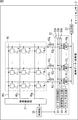
- FIG. 2 is a block diagram illustrating a configuration example of an image sensor 2.
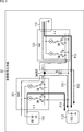
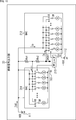
- FIG. 3 is a circuit diagram illustrating an outline of a configuration example of a reference signal output unit 33.
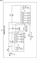
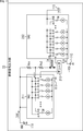
- FIG. 3 is a circuit diagram illustrating a first configuration example of a reference signal output unit 33.
- FIG. 6 is a timing chart illustrating an example of the operation of the first configuration example of the reference signal output unit 33.
- 12 is a timing chart for explaining another example of the operation of the first configuration example of the reference signal output unit 33.
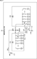
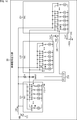
- 6 is a circuit diagram illustrating a second configuration example of a reference signal output unit 33.
- FIG. 10 is a timing chart illustrating an example of the operation of the second configuration example of the reference signal output unit 33.
- FIG. 6 is a circuit diagram illustrating a third configuration example of the reference signal output unit 33.
- 12 is a timing chart illustrating an example of the operation of the third configuration example of the reference signal output unit 33.
- FIG. 10 is a circuit diagram illustrating a fourth configuration example of the reference signal output unit 33.
- 12 is a timing chart illustrating an example of the operation of the fourth configuration example of the reference signal output unit 33.
- FIG. 10 is a circuit diagram illustrating a fifth configuration example of the reference signal output unit 33.
- FIG. 10 is a circuit diagram illustrating a sixth configuration example of the reference signal output unit 33.
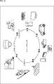
- 12 is a timing chart illustrating an example of the operation of the sixth configuration example of the reference signal output unit 33. It is a figure which shows the usage example which uses the image sensor.
- FIG. 1 is a block diagram illustrating a configuration example of an embodiment of a digital camera to which the present technology is applied.
- the digital camera can capture both still images and moving images.
- the digital camera includes an optical system 1, an image sensor 2, a memory 3, a signal processing unit 4, an output unit 5, and a control unit 6.
- the optical system 1 has, for example, a zoom lens, a focus lens, a diaphragm, and the like (not shown), and makes light from the outside enter the image sensor 2.
- the image sensor 2 is, for example, a CMOS (Complementary Metal Oxide Semiconductor) image sensor that receives incident light from the optical system 1, performs photoelectric conversion, and outputs image data corresponding to the incident light from the optical system 1. To do.
- CMOS Complementary Metal Oxide Semiconductor
- the memory 3 temporarily stores image data output from the image sensor 2.
- the signal processing unit 4 performs processing such as noise removal and white balance adjustment as signal processing using the image data stored in the memory 3 and supplies the processed signal to the output unit 5.
- the output unit 5 outputs the image data from the signal processing unit 4.
- the output unit 5 has a display (not shown) made of, for example, liquid crystal, and displays an image corresponding to the image data from the signal processing unit 4 as a so-called through image.
- the output unit 5 includes a driver (not shown) that drives a recording medium such as a semiconductor memory, a magnetic disk, or an optical disk, and records the image data from the signal processing unit 4 on the recording medium.
- a driver (not shown) that drives a recording medium such as a semiconductor memory, a magnetic disk, or an optical disk, and records the image data from the signal processing unit 4 on the recording medium.
- the control unit 6 controls each block constituting the digital camera in accordance with a user operation or the like.
- the image sensor 2 receives incident light from the optical system 1 and outputs image data according to the incident light.
- the image data output from the image sensor 2 is supplied to and stored in the memory 3.
- the image data stored in the memory 3 is subjected to signal processing by the signal processing unit 4, and the resulting image data is supplied to the output unit 5 and output.
- FIG. 2 is a block diagram showing a configuration example of the image sensor 2 of FIG.
- the image sensor 2 includes a pixel array 10, a control unit 20, a pixel driving unit 21, a column parallel AD conversion device 22, and an output unit 23.
- Pixel array 10, M ⁇ N number for photoelectric conversion (M and N is an integer of 1 or more) pixels 11 1,1, 11 1, 2, ⁇ ⁇ ⁇ , 11 1, N, 11 2,1, 11 2,2, ⁇ , 11 2, N, ⁇ , 11 M, 1, 11 M, 2, ⁇ , 11 M, has a N, imaging unit for capturing an image (image pickup device) Function as.
- M ⁇ N pixels 11 1,1 to 11 M, N are arranged in a matrix (lattice) of M rows and N columns on a two-dimensional plane.
- n-th column (n 1,2, ⁇ , N ) M pixels 11 1 arranged in the column direction (vertical direction) of, n to 11 M, the n, the column direction An extending VSL (Vertical Signal Line) 42 n is connected.
- the VSL42 n, pixel 11 1, n to 11 M, other n, the current source 43 n are connected.
- the pixel 11 m, n performs photoelectric conversion of light (incident light) incident thereon. Furthermore, the pixel 11 m, n outputs a voltage (electric signal) corresponding to the electric charge obtained by photoelectric conversion on the VSL 42 n according to the control from the pixel driving unit 21 via the pixel control line 41 m. .
- the pixels 11 m, n can perform photoelectric conversion of light of a predetermined color incident through a color filter (not shown) such as a Bayer array.
- the control unit 20 controls the pixel driving unit 21, the column parallel AD conversion device 22 (the auto zero control unit 32, the reference signal output unit 33, and the like) and other necessary blocks according to a predetermined logic or the like.
- Pixel driver 21 under the control of the control unit 20, via the pixel control line 41 m, to the pixels 11 m, 1 not connected to the pixel control line 41 m 11 m, and controls the N (drive).
- the column parallel AD converter 22 is connected to the pixels 11 m, 1 to 11 m, N arranged in each row via the VSLs 42 1 to 42 N , so that the pixels 11 m, n are output on the VSL 42 n.
- An electric signal (voltage) (hereinafter also referred to as a VSL signal) is supplied to the column parallel AD converter 22.
- the column parallel AD converter 22 performs column AD conversion of VSL signals supplied from the pixels 11 m, 1 to 11 m, N arranged in a row via the VSL 42 1 to 42 N in parallel.
- the digital data obtained as a result of AD conversion is supplied to the output unit 23 as pixel values (pixel data) of the pixels 11 m, 1 to 11 m, N.
- the column parallel AD converter 22 performs AD conversion of all the electric signals of the N pixels 11 m, 1 to 11 m, N arranged in a row in parallel, and the N pixels 11 m, 1. Moreover, AD conversion of electrical signals of one or more pixels of less than N out of 11 m, N can be performed in parallel.
- the column parallel AD converter 22 performs AD conversion of all VSL signals of N pixels 11 m, 1 to 11 m, N arranged in a row in parallel. To do.
- the column parallel AD converter 22 performs N ADC (Analog to Digital Converter) 31 in order to perform AD conversion of all VSL signals of N pixels 11 m, 1 to 11 m, N arranged in a row in parallel. 1 to 31 N.
- N ADC Analog to Digital Converter
- the column parallel AD converter 22 includes an auto zero control unit 32, a reference signal output unit 33, and a clock output unit 34.
- Auto-zero control unit 32 includes the ADC 31 n, supplying a signal for controlling an auto-zero process comparator not shown AZ pulse (auto-zero pulse), through the auto-zero control line 32A, the ADC 31 1 through 31 N (Output.
- AZ pulse auto-zero pulse
- the DC (Direct Current) level of the inverting input terminal and the non-inverting input terminal of the comparator included in the ADC 31 n is adjusted.
- the reference signal output unit 33 is composed of, for example, a DAC (Digital to Analog Converter), and the level (voltage) changes from a predetermined initial value to a predetermined final value with a constant slope like a ramp signal.
- a reference signal having a period is supplied (output) to the ADCs 31 1 to 31 N via the reference signal line 33A.
- a signal including a slope whose level (voltage) decreases at a constant change rate is adopted as the reference signal.
- the reference signal for example, a signal including a slope whose level increases at a constant change rate, a signal including a section in which the level is monotonously decreased or monotonously increased, etc. can be employed. .
- the clock output unit 34 supplies (outputs) a clock having a predetermined frequency to the ADCs 31 1 to 31 N via the clock line 34A.
- ADC 31 n is connected to VSL41 n, therefore, the ADC 31 n, the pixel 11 m, VSL signal n is outputted on VSL41 n (electrical signal) is supplied.
- the ADC 31 n performs AD conversion of the VSL signal output from the pixel 11 m, n using the reference signal from the reference signal output unit 33 and the clock from the clock output unit 34, and further performs CDS (Correlated Double Sampling). ) To obtain digital data as pixel values.
- the ADC 31 n compares the VSL signal of the pixel 11 m, n with the reference signal from the reference signal output unit 33 in a comparator (not shown), and compares the VSL signal of the pixel 11 m, n with the reference signal. Of the VSL signal of the pixel 11 m, n is counted by counting the time required for the level of the reference signal to change until the levels of the VSL signal match (until the magnitude relationship between the VSL signal and the reference signal is reversed) I do.
- the time required for the change in the level of the reference signal until the level of the VSL signal of the pixel 11 m, n matches the level of the reference signal is counted by counting the clock from the clock output unit 34. Is called.
- the N ADCs 31 1 to 31 N receive the VSL signals of the N pixels 11 m, 1 to 11 m, N in the first to M-th rows of the pixel array 10, for example, the first row. Are sequentially supplied, and AD conversion and CDS of the VSL signal are performed in units of rows.
- the output unit 23 selects a column n of reading the pixel values read from the ADC 31 n in the column n, the pixel 11 obtained in the ADC 31 n m, AD conversion of the n results (and CDS), as the pixel value And output to the outside (in this embodiment, the memory 3 (FIG. 1)).
- the ADC 31 n performs CDS in addition to AD conversion.
- the ADC 31 n performs only AD conversion, and CDS can be performed by the output unit 23.
- FIG. 3 is a circuit diagram showing an outline of a configuration example of the reference signal output unit 33.
- the reference signal output unit 33 includes, for example, two DACs 121 and 122 as a plurality of DACs, and a load resistor R that outputs a reference signal when a current flows.
- Each of the DACs 121 and 122 includes a plurality of current sources I and a plurality of switches SW having the same number as the number of the current sources I that control the current I flowing through each current source I.
- the number of current sources I may be the same or different.
- the current source I passes the current I.
- the current source I is controlled to be turned on / off according to the control of the control unit 20 (FIG. 2), for example. Further, in the present embodiment, each current source I passes the current I having the same value, but the currents passed by each current source I are, for example, 2 0 ⁇ I, 2 1 ⁇ I, 2 2 ⁇ I, .., 2 n ⁇ I,...
- the switch SW is connected to the current source I and controls the current I flowing by the current source I.
- the switch SW controls the current I flowing from the current source I connected to the switch SW by selecting the left terminal A or the right terminal B. That is, the current I flowing from the current source I flows to the terminal A when the switch SW selects the terminal A, and flows to the terminal B when the switch SW selects the terminal B.
- the reference signal output unit 33 is connected to, for example, three power supplies 111, 112, and 113 as three or more power supplies.
- the power source 111 is a positive power source with a positive voltage VDD (VDD> 0)
- the power source 112 is a negative power source with a negative voltage ⁇ VSS (VSS> 0).
- the power supply 113 is GND.
- GND is regarded as a power supply with a voltage of 0 V and is included in the power supply.
- the three or more power supplies connected to the reference signal output unit 33 need not include GND. That is, as the three or more power sources, for example, only a positive power source, only a negative power source, or only a positive power source and a negative power source can be employed. Similarly, the three or more power supplies may not include a positive power supply or a negative power supply. That is, as the three or more power supplies, for example, only a positive power supply and GND, or only a negative power supply and GND can be employed.
- three power supplies 111 to 113 as three or more power supplies connected to the reference signal output unit 33 are illustrated as being provided in the reference signal output unit 33.
- One or more power supplies can be provided outside the reference signal output unit 33.
- the current controlled by the switch SW of the DAC 121 or 122 flows in each combination of two or more power sources.
- the combination of two power sources out of the three power sources 111 to 113 connected to the reference signal output unit 33 includes a combination of the power source 111 and the power source 112, a combination of the power source 111 and the power source 113, There are three combinations of the power source 112 and the power source 113.
- the combination of the power source 111 and the power source 112 is a path P11 and P21 as a first path through which the current controlled by the switch SW of the DAC 121 flows.
- the path P11 is a path from the power supply 111 to the power supply 112 via the DAC 121
- the path P21 is a path from the power supply 111 to the power supply 112 via the DAC 121 and the load resistor R.
- the combination of the power supply 111 and the power supply 112 has a path P21 as a second path through which current flows in the same direction (in FIG. 3, from the upper end side to the lower end side) of the load resistance R.
- the path P21 is both the first path and the second path.
- the combination of the two power supplies 112 and 113 is the path P12 as the first path through which the current controlled by the switch SW of the DAC 122 flows. And P22.
- the path P12 is a path from the power supply 113 to the power supply 112 via the DAC 122
- the path P22 is a path from the power supply 113 to the power supply 112 via the DAC 122 and the load resistor R.
- the combination of the power source 112 and the power source 113 has a path P22 as a second path for flowing current in the same direction to the load resistance R.
- the path P22 is both the first path and the second path.
- route P21 or P22 there is a route (route P21 or P22) that is the second route apart from the route (route P11 or P12) that is the first route, but it is the first route.
- the route that is present and the route that is the second route do not necessarily have to exist as different routes. In other words, the route that is the first route and the route that is the second route may match.
- the reference signal output unit 33 in FIG. 3 includes a combination of the power source 111 and the power source 112 and a combination of the power source 112 and the power source 113 as the combinations of the power sources having the first path and the second path. Have street combinations.
- the power source 111 is connected to one end of each current source I of the DAC 121.
- the other end of the current source I is connected to the switch SW.
- the terminal A of the switch SW is connected to the lower end that is one end of the power source 112 and the load resistor R, and the terminal B of the switch SW is connected to the upper end that is the other end of the load resistor R.
- the power source 113 is connected to one end of each current source I of the DAC 122.
- the other end of the current source I is connected to the switch SW.
- the terminal A of the switch SW is connected to the upper end of the load resistor R, and the terminal B of the switch SW is connected to the power source 112 and the lower ends of the load resistor R.
- the current flowing from the current source I of the DAC 121 is supplied from the power supply 111 via the terminal A of the switch SW of the DAC 121 or the terminal B of the switch SW of the DAC 121. And, it flows to the power source 112 via the load resistance R.
- the current flowing from the current source I of the DAC 122 is supplied from the power source 113 via the terminal B of the switch SW of the DAC 122 or via the terminal A of the switch SW of the DAC 122 and the load resistor R. Then, it flows to the power source 112.
- the constant current I ⁇ N flows regardless of the selection of the terminal A or B by the switch SW of the DAC 122. It is possible to prevent an error from occurring in AD conversion in the ADC 31 n due to the fluctuation.
- the DAC 121 For example, paying attention to the DAC 121, when all the switches SW select the terminal B in the DAC 121, the current flowing through the load resistor R is maximized and the voltage DAOUT is maximized. In the DAC 121, as the number of switches SW that select the terminal A increases, the voltage DAOUT decreases. When all the switches SW select the terminal A, the current flowing through the load resistor R becomes 0, and the voltage DAOUT is , Be minimal.
- the reference signal DAOUT having a voltage in the range up to can be generated.
- each configuration example of the reference signal output unit 33 to be described includes a plurality of DACs including a plurality of current sources and a plurality of switches that control currents that the current sources flow; It has a load resistor that outputs a reference signal when current flows, and is connected to three or more power sources, and two or more types of power sources among a combination of two power sources out of three or more power sources Each of the combinations includes a first path through which a current controlled by the switch flows, and a second path through which current in the same direction flows through the load resistance.
- FIG. 4 is a circuit diagram showing a first configuration example of the reference signal output unit 33.
- the reference signal output unit 33 includes DACs 211 and 212, a decoder 213, and a load resistance R.
- the reference signal output unit 33 is connected to a power supply 111 having a positive voltage VDD, a power supply 112 having a negative voltage ⁇ VSS, and a power supply 113 being GND. That is, the DAC 211 is connected to the power supplies 111 and 113, and the DAC 212 is connected to the power supplies 111 and 112.
- Each of the DACs 211 and 212 includes a plurality of current sources I and a plurality of switches SW having the same number as the number of the current sources I that control the current I flowing through each current source I.
- the number of current sources I may be the same or different.
- one end of the current source I is connected to GND as the power source 113, and the other end of the current source I is connected to the switch SW.
- the switch SW selects the left terminal A or the right terminal B in accordance with the control of the decoder 213, thereby controlling the current I that the current source I connected to the switch SW flows.
- the terminal A is connected to the power source 111, and the terminal B is connected to the lower end of the load resistor R.
- one end of the current source I is connected to the power source 112, and the other end of the current source I is connected to the switch SW.
- the switch SW selects the left terminal A or the right terminal B in accordance with the control of the decoder 213, thereby controlling the current I that the current source I connected to the switch SW flows.
- the terminal A is connected to the lower end of the load resistor R, and the terminal B is connected to the power supply 111.
- the decoder 213 controls selection of the terminal A or B of the switches SW of the DACs 211 and 212 according to the control of the control unit 20 (FIG. 2), for example. That is, the decoder 213 counts the digital value according to the control of the control unit 20, and connects the terminal to the switch SW of the DACs 211 and 212 so that the (analog) current corresponding to the digital value flows through the load resistor R. Let A or B be selected.
- the terminal B of the DAC 211 and the terminal A of the DAC 212 are connected to the lower end of the load resistor R.
- the upper end of the load resistor R is connected to the power source 111, and the voltage DAOUT at the lower end of the load resistor R is output as the reference signal DAOUT.
- the combination of the power sources 111 and 113 connected to the DAC 211 is a path from the power source 111 to the power source 113 via the terminal A and the current source I of the DAC 211, and from the power source 111.
- a path reaching the power source 113 via the load resistor R, the terminal B of the DAC 211 and the current source I is a first path through which the current controlled by the switch SW of the DAC 211 flows.
- the combination of the power sources 111 and 113 is such that the path from the power source 111 to the power source 113 via the load resistor R, the terminal B of the DAC 211 and the current source I is in the same direction as the load resistor R (in this embodiment). , A direction from the top to the bottom).
- the combination of the power supplies 111 and 112 connected to the DAC 212 includes a path from the power supply 111 to the power supply 112 via the terminal B and the current source I of the DAC 212, and a load resistor R and a terminal of the DAC 212 from the power supply 111.
- a path that reaches the power source 112 via A and the current source I is a first path through which the current controlled by the switch SW of the DAC 212 flows.
- the combination of the power sources 111 and 112 is a second mode in which a current in the same direction flows through the load resistor R through the path from the power source 111 to the power source 112 via the load resistor R, the terminal A of the DAC 212 and the current source I. Have as a path.
- the DAC 211 exists on the first path and the second path that the combination of the power sources 111 and 113 connected to the DAC 211 has.
- the DAC 212 exists on the first path and the second path that the combination of the power sources 111 and 112 connected to the DAC 212 has.
- the current flowing from the current source I of the DAC 211 is supplied from the power supply 111 via the terminal A of the switch SW of the DAC 211 or the load resistor R and the DAC 211. It flows to the power source 113 via the terminal B of the switch SW.
- the DAC 211 generates a constant current I ⁇ N from the power supply 111 to the power supply 112 regardless of the selection of the terminal A or B by the switch SW of the DAC 211. Shed.
- the constant current I ⁇ N flows regardless of the selection of the terminal A or B by the switch SW of the DAC 211. It is possible to prevent an error from occurring in AD conversion in the ADC 31 n due to the fluctuation.
- the current that the current source I of the DAC 212 flows is supplied from the power source 111 via the terminal B of the switch SW of the DAC 212, or the load resistor R and the terminal A of the switch SW of the DAC 212. To the power source 112.
- the DAC 212 if the DAC 212 has N current sources I, the DAC 212 generates a constant current I ⁇ N from the power supply 111 to the power supply 112 regardless of the selection of the terminal A or B by the switch SW of the DAC 212. Shed.
- the constant current I ⁇ N flows regardless of the selection of the terminal A or B by the switch SW of the DAC 212. It is possible to prevent an error from occurring in AD conversion in the ADC 31 n due to the fluctuation.
- the current that flows from the power source 111 to the power source 113 via the terminal SW of the switch SW of the DAC 211 is the current that does not contribute to the generation of the reference signal DAOUT. In other words, it is a discarded current with the power source 111 as a disposal destination.
- the current flowing from the power source 111 to the power source 122 via the terminal B of the switch SW of the DAC 212 out of the current flowing from the current source I of the DAC 212 is a discarding current with the power source 111 as the discarding destination.
- the DAC 212 For example, paying attention to the DAC 212, when all the switches SW select the terminal B in the DAC 212, the current flowing through the load resistor R is minimized, and the voltage as the reference signal DAOUT is maximized. In the DAC 212, as the number of switches SW for selecting the terminal A increases, the current flowing through the load resistor R increases, and the voltage as the electric reference signal DAOUT decreases. In the DAC 212, when all the switches SW select the terminal A, the current flowing through the load resistor R is maximized, and the voltage as the reference signal DAOUT is minimized.
- the DAC 212 is connected to the power supply 111 of the positive voltage VDD and the power supply 112 of the negative voltage ⁇ VSS, so that only the DAC 212 of the DACs 211 and 212 is operated.
- the switch SW of the DAC 212 By controlling the current flowing through the load resistor R by the switch SW of the DAC 212, it is possible to generate the reference signal DAOUT having a voltage ranging from a positive voltage equal to or lower than the positive voltage VDD to a negative voltage equal to or higher than the negative voltage ⁇ VSS. .
- Idd current flowing from the positive voltage VDD power supply 111
- Iss current flowing into the negative voltage ⁇ VSS power supply 112
- the currents Idd and Iss are constant currents I ⁇ N. .
- the reference signal DAOUT can be generated.
- the current that the DAC 212 flows flows between the positive voltage VDD power supply 111 and the negative voltage-VSS power supply 112. Therefore, the power consumption due to the current flowing through the DAC 212 is the product of the current and the voltage VDD + VSS.
- the DAC 211 connected to the power supply 111 having the positive voltage VDD and the power supply 113 being the GND generates the reference signal DAOUT having a voltage ranging from the positive voltage VDD or lower to the GND voltage, that is, the voltage ranging from 0V. can do.
- the current that the DAC 211 flows flows between the power supply 111 of the positive voltage VDD and the power supply 113 that is GND. Therefore, the power consumption due to the current flowing through the DAC 211 is the product of the current and the voltage VDD.
- the power consumption due to the current flowing through the DAC 212 is equal to the negative voltage ⁇ VSS of the power supply 112 connected to the DAC 212. Therefore, the power consumption is greater than the current consumed by the DAC 211. In other words, the power consumption due to the current flowing through the DAC 211 is smaller than the power consumption due to the current flowing through the DAC 212.
- the reference signal DAOUT having a voltage in the range from the positive voltage to the negative voltage can be generated, but the power consumption increases.
- the DAC 211 only the reference signal DAOUT having a voltage in the range from the positive voltage to 0V can be generated, that is, the negative voltage reference signal DAOUT cannot be generated, but the power consumption is reduced. Become.
- the reference signal output unit 33 changes the DAC used for the output of the reference signal DAOUT according to the range of the voltage output as the reference signal DAOUT, thereby referring to the voltage in the range from the positive voltage to the negative voltage.
- the signal DAOUT can be output and the power consumption is suppressed.
- the DAC 211 of the DACs 211 and 212 is used to output the reference signal DAOUT having a voltage ranging from a positive voltage to 0V.
- the DAC 212 is used to output the reference signal DAOUT having a voltage in the range from 0V to a negative voltage.
- FIG. 5 is a timing chart for explaining an example of the operation of the reference signal output unit 33 of FIG.
- FIG. 5 shows an example of the current Idd flowing through the power supply 111, the current Iss flowing through the power supply 112, the on / off state of the current source I of the DACs 211 and 212, and the reference signal DAOUT.
- the number of the current sources I of the DAC 211 and the number of the current sources I of the DAC 212 are both N.
- the current flowing through the DAC 211 and the current flowing through the DAC 212 are both I ⁇ N constant currents.
- the output of the reference signal DAOUT in the voltage range from the positive voltage to 0V is turned on as shown in FIG.
- the current source I of the DAC 212 is controlled to be off.
- the decoder 213 controls the switch SW so that the number of the switches SW for selecting the terminal B from the terminal A is increased in the DAC 211 in which the current source I is turned on, whereby the reference signal DAOUT is shown in FIG. As shown, it gradually decreases.
- the current source I of the DAC 212 is off while the positive voltage reference signal DAOUT is being output, the current flowing through the DAC 212 is 0, and the current Iss flowing through the power supply 112 connected to the DAC 212 is also , 0.
- the current source I of the DAC 211 is controlled to be off, and the current source I of the DAC 212 is controlled to be on.
- the current flowing through the DAC 212 is equal to the current I ⁇ N flowing through the DAC 211 before turning off, and the current Iss flowing through the power supply 112 connected to the DAC 212 is the current I ⁇ N flowing through the DAC 212 as shown in FIG. become.
- the current Idd flowing through the power supply 111 has a current flowing through the DAC 211 from I ⁇ N to 0, while the current flowing through the DAC 212 is from 0 to I ⁇ N. Therefore, as shown in FIG. Will remain.
- the decoder 213 controls the switch SW so that the number of the switches SW that select the terminal A from the terminal B in the on-DAC 212 is increased, whereby the reference signal DAOUT is gradually increased as shown in FIG. It goes down.
- the DAC used for outputting the reference signal DAOUT by controlling on / off of the current source I of the DACs 211 and 212 in accordance with the range of the voltage output as the reference signal DAOUT, the DAC used for outputting the reference signal DAOUT, and thus the load resistance
- the path of the current flowing through R is changed from a path passing through the DAC 211 to a path passing through the DAC 212.
- the DAC 211 connected to the (positive) power supply 111 of the positive voltage VDD is operated, and the path passing through the DAC 211.
- the DAC 212 connected to the negative voltage-VSS (negative) power supply 112 is operated, and the current is passed through the load resistor R through the DAC 212.
- power consumption can be suppressed.
- the DAC 211 (current source I) is turned on when the positive voltage reference signal DAOUT is output, the DAC 212 is turned off, and the DAC 211 is turned off and the DAC 212 is turned on when the negative voltage reference signal DAOUT is output.
- the power consumption can be suppressed when the reference signal DAOUT having a voltage in the range from the positive voltage to the negative voltage is output.
- the power consumption P can be suppressed by the amount that the power consumption P when the positive voltage reference signal DAOUT is output decreases from Vdd ⁇ Idd + Vss ⁇ Iss to Vdd ⁇ Idd.
- the decoder 213 When switching from the DAC 211 to the DAC 212, that is, when the DAC 211 is turned off and the DAC 212 is turned on, the decoder 213 causes the current that the DAC 211 is flowing through the load resistor R immediately before switching and the DAC 212 to be switched immediately after switching. Selection of the terminal A or B of the switch SW in the DAC 212 is controlled so that the current flowing through the load resistor R becomes equal.
- FIG. 6 is a timing chart for explaining another example of the operation of the reference signal output unit 33 of FIG.
- FIG. 6 shows another example of the current Idd flowing through the power source 111, the current Iss flowing through the power source 112, the on / off state of the current source I of the DACs 211 and 212, and the reference signal DAOUT.
- a DAC used to output the reference signal DAOUT that is, a DAC that passes a current flowing through the load resistor R is also referred to as an effective DAC, and a DAC that is not an effective DAC is also referred to as an invalid DAC.
- the reference signal DAOUT becomes 0 V, which is the minimum voltage that can be output using the DAC 211
- the effective DAC is instantaneously switched from the DAC 211 to the DAC 212. In other words, it can be performed gradually (smoothly).
- the N current sources I in which the DAC 211 is turned on are, for example, one or more each. Are sequentially controlled off.
- the N current sources I in which the DAC 212 is turned off are sequentially turned on by the number of current sources I turned off in the DAC 211, as shown in FIG.
- the current sources I of the DAC 212 are turned on by the number of current sources I turned off by the DAC 211, the total amount of current flowing through the DACs 211 and 212, that is, the current Idd flowing through the power source 111 is As shown in FIG. 6, I ⁇ N remains constant.
- the current Iss flowing from the DAC 212 to the power source 112 increases with an increase in the current source I that is turned on in the DAC 212, that is, when the reference signal DAOUT becomes 0V, that is, I ⁇ N when all current sources I are turned off and all current sources I of DAC 212 are turned on.
- the DACs 211 and 212 distribute the current flowing through the load resistor R by the current source I that is turned on.
- the decoder 213 controls the switches SW of the DACs 211 and 212 so that a current for obtaining the reference signal DAOUT having a desired voltage flows through the load resistor R.
- the reference signal DAOUT may become unstable when the effective DAC is switched.
- the path of the current flowing through the load resistor R is changed from the DAC 211 to both the DACs 211 and 212, and finally switched to the DAC 212, so that the current flows through the load resistor R. It is possible to prevent the reference signal DAOUT from becoming unstable by instantaneously switching the current path to another path.
- the power consumption can be suppressed as in the case of FIG.
- the current source I of the DAC 212 in order to gradually switch the effective DAC, that is, until the reference signal DAOUT becomes 0V from a predetermined voltage before becoming 0V, the current source I of the DAC 212 is sequentially changed. , The current Iss flowing from the DAC 212 to the power source 112 gradually increases.
- the power consumption is reduced by the amount of the current Iss flowing through the power source 112 gradually increasing from the predetermined voltage before the reference signal DAOUT becomes 0V to 0V.
- the reference signal DAOUT can be prevented from becoming unstable as described above.
- the effective DAC can be switched gradually, but for the sake of simplicity, the following embodiment is an example in which the effective DAC is switched instantaneously. Explained.
- FIG. 7 is a circuit diagram showing a second configuration example of the reference signal output unit 33.
- the reference signal output unit 33 includes a decoder 213, DACs 221 and 222, and a load resistor R.
- the reference signal output unit 33 of FIG. 7 has a decoder 213 and a load resistance R, and is common to the case of FIG. 4, except that DACs 221 and 222 are provided instead of the DACs 211 and 212, respectively. This is different from the case of FIG.
- the reference signal output unit 33 is connected to a power supply 111 having a positive voltage VDD, a power supply 112 having a negative voltage ⁇ VSS, and a power supply 113 being a GND. That is, the DAC 221 is connected to the power sources 111 and 112, and the DAC 222 is connected to the power sources 112 and 113.
- Each of the DACs 221 and 222 includes a plurality of current sources I and a plurality of switches SW having the same number as the number of the current sources I that control the current I flowing through each current source I.
- the number of current sources I may be the same or different.
- one end of the current source I is connected to the power source 111, and the other end of the current source I is connected to the switch SW.
- the switch SW selects the left terminal A or the right terminal B according to the control of the decoder 213, and thereby controls the current I that the current source I connected to the switch SW flows.
- the terminal A is connected to the upper end of the load resistor R, and the terminal B is connected to the power source 112.
- one end of the current source I is connected to GND as the power source 113, and the other end of the current source I is connected to the switch SW.
- the switch SW selects the left terminal A or the right terminal B in accordance with the control of the decoder 213, thereby controlling the current I that the current source I connected to the switch SW flows.
- the terminal A is connected to the power source 112, and the terminal B is connected to the upper end of the load resistor R.
- the switches SW of the DACs 221 and 222 are controlled by the decoder 213. That is, the decoder 213 counts the digital value according to the control of the control unit 20 (FIG. 2), and switches the DACs 221 and 222 so that the (analog) current corresponding to the digital value flows through the load resistor R. Have SW select terminal A or B.
- the terminal A of the DAC 221 and the terminal B of the DAC 222 are connected to the upper end of the load resistor R.
- the lower end of the load resistor R is connected to the power supply 112, and the voltage DAOUT at the upper end of the load resistor R is output as the reference signal DAOUT.
- the combination of the power sources 111 and 112 connected to the DAC 221 includes a path from the power source 111 to the power source 112 via the current source I and the terminal B of the DAC 221, and the power source 111.
- a path to the power source 112 via the current source I, the terminal A, and the load resistor R of the DAC 221 is a first path through which the current controlled by the switch SW of the DAC 221 flows.
- the combination of the power sources 111 and 112 causes currents in the same direction to flow through the path from the power source 111 to the power source 112 via the current source I of the DAC 221, the terminal A, and the load resistor R. As a second path.
- the combination of the power sources 112 and 113 connected to the DAC 222 includes a path from the power source 113 to the power source 112 via the current source I, the terminal A, and the current source I of the DAC 222, and the current of the DAC 222 from the power source 113.
- a path that reaches the power source 112 via the source I, the terminal B, and the load resistor R is a first path through which a current controlled by the switch SW of the DAC 222 flows.
- the combination of the power sources 112 and 113 allows current in the same direction to flow through the load resistor R through the path from the power source 113 to the power source 112 via the current source I of the DAC 222, the terminal B, and the load resistor R. As a second path.
- the DAC 221 exists on the first path and the second path that the combination of the power sources 111 and 112 connected to the DAC 221 has.
- the DAC 222 exists on the first path and the second path that the combination of the power sources 112 and 113 connected to the DAC 222 has.
- the current flowing from the current source I of the DAC 221 is supplied from the power source 111 via the terminal B of the switch SW of the DAC 221 or the terminal B of the switch SW of the DAC 221. And, it flows to the power source 112 via the load resistance R.
- the DAC 221 if the DAC 221 has N current sources I, the DAC 221 generates a constant current I ⁇ N from the power supply 111 to the power supply 113 regardless of the selection of the terminal A or B by the switch SW of the DAC 221. Shed.
- the current that the current source I of the DAC 222 flows flows from the power supply 113 via the terminal A of the switch SW of the DAC 222 or the terminal B of the switch SW of the DAC 222 and the load resistance R. To the power source 112.
- the DAC 222 generates a constant current I ⁇ N from the power supply 113 to the power supply 112 regardless of the selection of the terminal A or B by the switch SW of the DAC 222. Shed.
- the constant current I ⁇ N flows regardless of the selection of the terminal A or B by the switch SW of the DAC 222. It is possible to prevent an error from occurring in AD conversion in the ADC 31 n due to the fluctuation.
- the current that flows from the power source 111 to the power source 112 via the switch SW terminal B of the DAC 221 out of the current that flows from the current source I of the DAC 221 does not contribute to the generation of the reference signal DAOUT. This is a discarded current with the power source 112 as a disposal destination.
- the current flowing from the current source I of the DAC 222 is a discarding current with the GND as the power source 113 as the discarding destination. is there.
- the DAC 221 For example, paying attention to the DAC 221, when all the switches SW select the terminal A in the DAC 221, the current flowing through the load resistor R is maximized, and the voltage as the reference signal DAOUT is maximized. Further, in the DAC 221, as the number of switches SW for selecting the terminal B increases, the current flowing through the load resistor R decreases, and the voltage as the reference signal DAOUT decreases. In the DAC 221, when all the switches SW select the terminal B, the current flowing through the load resistor R is minimized, and the voltage as the reference signal DAOUT is minimized.
- the DAC 221 is connected to the power supply 111 of the positive voltage VDD and the power supply 112 of the negative voltage ⁇ VSS, so that only the DAC 221 out of the DACs 221 and 222 is operated.
- the switch SW of the DAC 221 By controlling the current flowing through the load resistor R by the switch SW of the DAC 221, it is possible to generate the reference signal DAOUT having a voltage ranging from a positive voltage equal to or lower than the positive voltage VDD to a negative voltage equal to or higher than the negative voltage ⁇ VSS. .
- the current Idd that flows from the power supply 111 with the positive voltage VDD and the current Iss that flows into the power supply 113 with the negative voltage ⁇ VSS become the constant current I ⁇ N.
- the negative voltage ⁇ VSS power source 112 and the power source 113 that is GND are provided in addition to the DAC 221 connected to the positive voltage VDD power source 111 and the negative voltage ⁇ VSS power source 112, the negative voltage ⁇ VSS power source 112 and the power source 113 that is GND are provided. It has a DAC 222 connected.
- the voltage ranges from the positive voltage VDD or lower to the negative voltage ⁇ VSS or higher negative voltage.
- the reference signal DAOUT can be generated.
- the current that the DAC 221 flows flows between the positive voltage VDD power supply 111 and the negative voltage -VSS power supply 112. Therefore, the power consumption due to the current flowing through the DAC 221 is the product of the current and the voltage VDD + VSS.
- the reference signal DAOUT having a voltage in the range from the GND voltage 0 V to the negative voltage ⁇ VSS or more is obtained. Can be generated.
- the current that the DAC 222 flows flows between the negative voltage ⁇ VSS power source 112 and the power source 113 that is GND. Therefore, the power consumption due to the current flowing through the DAC 222 is the product of the current and the voltage VSS.
- the power consumption due to the current flowing through the DAC 221 is the negative voltage ⁇ VSS of the power supply 112 connected to the DAC 221. Accordingly, the power consumption is larger than the power consumed by the current that the DAC 222 flows. In other words, the power consumption due to the current flowing through the DAC 222 is smaller than the power consumption due to the current flowing through the DAC 221.
- the DAC 221 can generate the reference signal DAOUT having a voltage in the range from the positive voltage to the negative voltage, but the power consumption increases.
- the DAC 222 can generate only the reference signal DAOUT having a voltage ranging from 0V to a negative voltage, that is, it cannot generate the positive reference signal DAOUT, but the power consumption is reduced. Become.
- the reference signal output unit 33 changes the DAC used for the output of the reference signal DAOUT according to the range of the voltage output as the reference signal DAOUT, thereby referring to the voltage in the range from the positive voltage to the negative voltage.
- the signal DAOUT can be output and the power consumption is suppressed.
- the DAC 221 of the DACs 221 and 222 is used as an effective DAC for outputting the reference signal DAOUT having a voltage ranging from a positive voltage to 0V.
- the DAC 222 is used as an effective DAC for outputting the reference signal DAOUT having a voltage in the range from 0 V to a negative voltage.
- FIG. 8 is a timing chart for explaining an example of the operation of the reference signal output unit 33 of FIG.
- FIG. 8 shows an example of the current Idd flowing through the power supply 111, the current Iss flowing through the power supply 112, the on / off state of the current source I of the DACs 221 and 222, and the reference signal DAOUT.
- the number of the current sources I of the DAC 221 and the number of the current sources I of the DAC 222 are both N.
- the current flowing through the DAC 221 and the current flowing through the DAC 222 are both I ⁇ N constant currents.
- the output of the reference signal DAOUT in the voltage range from the positive voltage to 0V is turned on as shown in FIG.
- the current source I of the DAC 222 is controlled to be off.
- the decoder 213 controls the switch SW so that the number of the switches SW for selecting the terminal B from the terminal A is increased in the DAC 221 (the current source I is turned on), whereby the reference signal DAOUT is shown in FIG. As shown, it gradually decreases.
- the current source I of the DAC 222 is off, so the current that the DAC 222 flows becomes zero.
- the current Iss flowing in the power source 112 into which the current flowing through the DACs 221 and 222 flows becomes a constant current I ⁇ N.
- the current source I of the DAC 221 is controlled to be off, and the current source I of the DAC 222 is controlled to be on.
- the current Iss flowing through the power supply 112 is changed from 0 ⁇ I ⁇ N while the current flowing through the DAC 221 connected to the power supply 112 changes from I ⁇ N to 0, while the current flowing through the DAC 222 connected to the power supply 112 changes from 0 ⁇ I ⁇ N As shown in FIG. 8, I ⁇ N remains unchanged.
- the decoder 213 controls the switch SW so that the number of the switches SW for selecting the terminal A from the terminal B in the on-DAC 222 is increased, whereby the reference signal DAOUT is gradually increased as shown in FIG. It goes down.
- the DAC used for the output of the reference signal DAOUT is changed according to the range of the voltage output as the reference signal DAOUT, and in the range of DAOUT> 0, the (positive) power supply 111 of the positive voltage VDD and the negative
- the DAC 221 connected to the voltage -VSS power source 112 is operated, and in the range of DAOUT ⁇ 0, the negative voltage -VSS (negative) power source 112 and the DAC 222 connected to the power source 113 which is GND are operated. Electric power can be suppressed.
- the DAC 221 (current source I) is turned on when the positive voltage reference signal DAOUT is output, the DAC 222 is turned off, and the DAC 221 is turned off and the DAC 222 is turned on when the negative voltage reference signal DAOUT is output.
- the power consumption can be suppressed when the reference signal DAOUT having a voltage in the range from the positive voltage to the negative voltage is output.
- the power consumption can be suppressed by the amount that the power consumption P when the negative voltage reference signal DAOUT is output decreases from Vdd ⁇ Idd + Vss ⁇ Iss to Vss ⁇ Iss.
- the decoder 213 causes the current that the DAC 221 is flowing to the load resistance R immediately before the switching and the DAC 222 to Selection of the terminal A or B of the switch SW in the DAC 222 is controlled so that the current flowing through the load resistor R becomes equal.
- FIG. 9 is a circuit diagram showing a third configuration example of the reference signal output unit 33.
- the reference signal output unit 33 includes a decoder 213, DACs 231 and 232, and a load resistance R.
- the reference signal output unit 33 of FIG. 9 has a decoder 213 and a load resistance R, and is common to the case of FIG. 4, and DACs 231 and 232 are provided instead of the DACs 211 and 212, respectively. This is different from the case of FIG.
- the reference signal output unit 33 is connected to a power supply 111 having a positive voltage VDD, a power supply 112 having a negative voltage ⁇ VSS, and a power supply 113 being GND. That is, the DAC 231 is connected to the power sources 111 and 113, and the DAC 232 is connected to the power sources 111 and 112.
- Each of the DACs 231 and 232 includes a plurality of current sources I and a plurality of switches SW having the same number as the number of the current sources I for controlling the current I flowing through each current source I.
- the number of current sources I may be the same or different.
- one end of the current source I is connected to the power source 113, and the other end of the current source I is connected to the switch SW.
- the switch SW is turned on / off according to the control of the decoder 213, thereby controlling the current I that the current source I connected to the switch SW flows.
- the connection between the lower end of the load resistor R and the current source I is turned on / off by turning on / off the switch SW.
- one end of the current source I is connected to the power source 112, and the other end of the current source I is connected to the switch SW.
- the switch SW is turned on / off according to the control of the decoder 213, thereby controlling the current I flowing from the current source I connected to the switch SW.
- the switches SW of the DACs 231 and 232 are controlled by the decoder 213. That is, the decoder 213 counts the digital value according to the control of the control unit 20 (FIG. 2), and switches the DACs 231 and 232 so that the (analog) current corresponding to the digital value flows through the load resistor R. Turn SW on / off.
- the lower end of the load resistor R is connected to the current source I of the DAC 231 via the switch SW of the DAC 231 and is connected to the current source I of the DAC 232 via the switch SW of the DAC 232.
- the upper end of the load resistor R is connected to the power source 111, and the voltage DAOUT at the lower end of the load resistor R is output as the reference signal DAOUT.
- the combination of the power sources 111 and 113 connected to the DAC 231 has a path from the power source 111 to the power source 113 via the load resistor R and the current source I of the DAC 231.
- the first path through which the current controlled by the switch SW of the DAC 231 flows and the second path through which the current in the same direction flows through the load resistor R are provided.
- the combination of the power sources 111 and 112 connected to the DAC 232 is controlled by the switch SW of the DAC 232 along the path from the power source 111 to the power source 112 via the load resistance R and the current source I of the DAC 232.
- the first path through which current flows and the second path through which current flows in the same direction through the load resistor R are provided.
- the DAC 231 exists on the first path and the second path that the combination of the power sources 111 and 113 connected to the DAC 231 has.
- the DAC 232 exists on the first path and the second path included in the combination of the power supplies 111 and 112 connected to the DAC 232.
- a current flowing from the current source I in which the switch SW is turned on flows in the DAC 231, and the current flows from the power source 111 to the load resistor R and the DAC 231. Via the power source 113.
- a current flowing from the current source I with the switch SW turned on flows, and the current flows from the power source 111 to the power source 112 via the load resistor R and the DAC 232.
- the DAC 232 For example, paying attention to the DAC 232, when all the switches SW are turned off in the DAC 232, the current flowing through the load resistor R is minimized, and the voltage as the reference signal DAOUT is maximized. In the DAC 232, as the number of ON switches SW increases, the current flowing through the load resistor R increases, and the voltage as the reference signal DAOUT decreases. In the DAC 232, when all the switches SW are turned on, the current flowing through the load resistor R is maximized, and the voltage as the reference signal DAOUT is minimized.
- the DAC 232 is connected to the power supply 111 of the positive voltage VDD and the power supply 112 of the negative voltage ⁇ VSS, so that only the DAC 232 of the DACs 231 and 232 is operated, By controlling the current flowing through the load resistor R by the switch SW of the DAC 232, it is possible to generate the reference signal DAOUT having a voltage ranging from a positive voltage equal to or lower than the positive voltage VDD to a negative voltage equal to or higher than the negative voltage ⁇ VSS. .
- the power consumption P of the reference signal output unit 33 is the voltage VDD of the power supply 111 connected to the DAC 232.
- the reference signal DAOUT can be generated.
- the current that the DAC 232 flows flows between the positive voltage VDD power supply 111 and the negative voltage -VSS power supply 112. Therefore, the power consumption due to the current flowing through the DAC 232 is the product of the current and the voltage VDD + VSS.
- the DAC 231 connected to the power supply 111 having the positive voltage VDD and the power supply 113 being the GND generates the reference signal DAOUT having a voltage in the range from the positive voltage equal to or lower than the positive voltage VDD to 0V being the GND voltage. be able to.
- the current that the DAC 231 flows flows between the power supply 111 having a positive voltage VDD and the power supply 113 being GND. Therefore, the power consumption due to the current flowing through the DAC 231 is the product of the current and the voltage VDD.
- the power consumption due to the current flowing through the DAC 232 is equal to the negative voltage ⁇ VSS of the power supply 112 connected to the DAC 232. Accordingly, the power consumption is larger than the current consumed by the DAC 231. In other words, the power consumption due to the current flowing through the DAC 231 is smaller than the power consumption due to the current flowing through the DAC 232.
- the DAC 232 can generate the reference signal DAOUT having a voltage ranging from the positive voltage to the negative voltage, but the power consumption increases.
- the DAC 232 can generate only the reference signal DAOUT having a voltage in the range from the positive voltage to 0V, that is, it cannot generate the negative voltage reference signal DAOUT, but the power consumption is reduced. Become.
- the reference signal output unit 33 changes the DAC used for the output of the reference signal DAOUT according to the range of the voltage output as the reference signal DAOUT, thereby referring to the voltage in the range from the positive voltage to the negative voltage.
- the signal DAOUT can be output and the power consumption is suppressed.
- the DAC 231 of the DACs 231 and 232 is used as an effective DAC for outputting the reference signal DAOUT having a voltage ranging from a positive voltage to 0V.
- the DAC 232 is used as an effective DAC for outputting the reference signal DAOUT having a voltage ranging from 0V to a negative voltage.
- the upper end of the load resistor R is connected to the power source 111 of the positive voltage VDD, and the voltage DAOUT at the lower end of the load resistor R is used as the reference signal DAOUT.
- the reference signal output unit 33 having the DACs 231 and 232 has the same configuration as that of FIG. However, a configuration in which the voltage DAOUT at the upper end of the load resistor R is output as the reference signal DAOUT (hereinafter also referred to as a negative voltage reference configuration) can be employed.
- the reference signal output unit 33 As the configuration of the reference signal output unit 33, either a positive voltage reference configuration or a negative voltage reference configuration can be adopted.
- FIG. 10 is a timing chart for explaining an example of the operation of the reference signal output unit 33 of FIG.
- FIG. 10 shows an example of the current Idd flowing through the power supply 111, the current Iss flowing through the power supply 112, the on / off state of the current source I of the DACs 231 and 232, and the reference signal DAOUT.
- the output of the reference signal DAOUT in the voltage range from the positive voltage to 0 V is turned on as shown in FIG.
- the current source I of the DAC 232 is controlled to be turned off.
- the decoder 213 controls the switch SW so that the number of the switches SW that are turned on from the off state is increased in the DAC 231 that is on (the current source I is turned on), so that the reference signal DAOUT is as shown in FIG. , Gradually decline.
- the current source I of the DAC 232 is off, so the current that the DAC 232 flows becomes zero.
- the current Idd that the power supply 111 passes through the DACs 231 and 232 increases in accordance with the number of switches SW that are turned on in the DAC 231.
- the reference signal DAOUT becomes 0 V, which is the minimum voltage that can be output using the DAC 231 (and without using the DAC 232)
- the output of the reference signal DAOUT having a negative voltage thereafter is shown in FIG.
- the current source I of the DAC 231 is controlled to be off, and the current source I of the DAC 232 is controlled to be on.
- the DAC 231 is turned off and the DAC 232 is turned on.
- the decoder 213 causes the current that the DAC 231 is flowing to the load resistance R immediately before the switching, and the DAC 232 is the load resistance R immediately after the switching.
- the switch SW of the DAC 232 is controlled to be turned on so that the current flowing through is equal.
- the current Iss flowing through the power source 122 connected to the DAC 232 also changes from 0 to a predetermined value.
- the current Idd flowing through the power supply 111 remains at a predetermined value as shown in FIG. 10 because the current flowing through the DAC 231 changes from a predetermined value to 0 while the current flowing through the DAC 232 changes from 0 to a predetermined value. .
- the decoder 213 controls the switch SW so that the number of the switches SW that are turned on from the off state is increased in the DAC 232 that is turned on, whereby the reference signal DAOUT gradually decreases as shown in FIG. I will do it.
- the DAC used to output the reference signal DAOUT is changed according to the range of the voltage output as the reference signal DAOUT, and connected to the (positive) power supply 111 of the positive voltage VDD in the range of DAOUT> 0.
- the power consumption can be suppressed by operating the DAC 231 and operating the DAC 232 connected to the (negative) power source 112 of the negative voltage ⁇ VSS in the range of DAOUT ⁇ 0.
- the DAC 231 current source I
- the DAC 232 is turned off.
- the negative voltage reference signal DAOUT is output
- the DAC 231 is turned off and the DAC 232 is turned on.
- the power consumption P can be suppressed by the amount that the power consumption P when the positive voltage reference signal DAOUT is output decreases from Vdd ⁇ Idd + Vss ⁇ Iss to Vdd ⁇ Idd.
- FIG. 11 is a circuit diagram illustrating a fourth configuration example of the reference signal output unit 33.
- the reference signal output unit 33 includes DACs 211 and 212, a decoder 213, and load resistors Ro1 and Ro2.
- the reference signal output unit 33 of FIG. 11 is common to the case of FIG. 4 in that it includes DACs 211 and 212 and a decoder 213, and instead of one load resistor R, two load resistors Ro1 and It differs from the case of FIG. 4 in having Ro2.
- the lower end of the load resistor R whose upper end is connected to the power source 111 is connected to the terminal B of the DAC 211 and the terminal A of the DAC 212, but in FIG. 11, the upper end is connected to the power source 111.
- the lower end of the load resistor Ro1 is connected to the terminal B of the DAC 211 and the upper end of the load resistor Ro2, and the lower end of the load resistor Ro2 is connected to the terminal A of the DAC 212.
- the voltage DAOUT at the lower end of the load resistor Ro2 is output as the reference signal DAOUT.
- the DAC used to output the reference signal DAOUT is By changing according to the range of the voltage output as the reference signal DAOUT, it is possible to output the reference signal DAOUT with a voltage in the range from the positive voltage to the negative voltage and to suppress power consumption.
- the DAC 211 of the DACs 211 and 212 is used as an effective DAC for the output of the reference signal DAOUT having a voltage in the range from positive voltage to 0V.
- the power consumption can be suppressed by using the DAC 212 as an effective DAC.
- FIG. 12 is a timing chart for explaining an example of the operation of the reference signal output unit 33 of FIG.
- FIG. 12 shows the current Idd flowing through the power supply 111, the current Iss flowing through the power supply 112, the current Ia flowing from the load resistance Ro2 into the DAC 212, and the current Id flowing from the power supply 111 into the DAC 212 and the currents Ib flowing into the DAC 212.
- An example of the on / off state of the current source I and the reference signal DAOUT is shown.
- the output of the reference signal DAOUT in the voltage range from the positive voltage to 0 V is turned on as shown in FIG.
- the current source I of the DAC 212 is controlled to be off.
- the decoder 213 controls the switch SW so that the number of the switches SW for selecting the terminal B from the terminal A is increased in the DAC 211 in which the current source I is turned on. As shown, it gradually decreases.
- the current Idd flowing through the power supply 111 becomes a constant current flowing through the DAC 211 (all of the current sources I thereof).
- the current source I of the DAC 212 is off while the positive voltage reference signal DAOUT is output, the current flowing through the DAC 212 is 0, and the currents Ia and Ib flowing through the DAC 212 and the DAC 212 are connected. The current Iss flowing through the power source 112 is also zero.
- the voltage at the lower end of the load resistor Ro2 is equal to the voltage at the lower end of the load resistor Ro1, and this voltage is output as the reference signal DAOUT.
- the reference signal DAOUT becomes 0 V, which is the minimum voltage that can be output using the DAC 211 (and not using the DAC 212)
- the subsequent output of the reference signal DAOUT with a negative voltage is shown in FIG. 12, for example, the current source I of the DAC 211 remains on, and the current source I of the DAC 212 is controlled to be on.
- the DAC 211 When the current source I of the DAC 211 is kept on, the DAC 211 continues to pass the current when the reference signal DAOUT becomes 0V.
- the current that the DAC 212 flows that is, the current Iss that flows from the DAC 212 to the power source 112 is changed from 0 to each of the current sources I of the DAC 212 as shown in FIG. Becomes a predetermined value equal to the sum of the currents flowing.
- the DAC 211 keeps flowing current, and the current flowing through the DAC 212 changes from 0 to a predetermined value, so that it flows from the power supply 111 equal to the sum of the currents flowing through the DACs 211 and 212.
- the current Idd increases by a predetermined value as a current that the DAC 212 flows.
- the reference signal DAOUT that is, the voltage at the lower end of the load resistor Ro2 is a voltage that is changed by the voltage drop of the load resistor Ro2 from the voltage at the lower end of the load resistor Ro1.
- the decoder 213 controls the switch SW so that the number of the switches SW for selecting the terminal A from the terminal B in the on-DAC 212 is increased.
- the current Ia flowing from the load resistor Ro2 to the terminal A increases and the current Ib flowing from the power source 111 to the terminal B decreases, which is the voltage at the lower end of the load resistor Ro2.
- the reference signal DAOUT gradually decreases as shown in FIG.
- the DAC used for the output of the reference signal DAOUT is changed by controlling on / off of the current source I of the DAC 212 according to the range of the voltage output as the reference signal DAOUT, and DAOUT> 0
- the DAC 211 connected to the (positive) power supply 111 of the positive voltage VDD is operated, and in the range of DAOUT ⁇ 0, the DAC 212 connected to the (negative) power supply 112 of the negative voltage ⁇ VSS is operated in addition to the DAC 211. By making it, power consumption can be suppressed.
- the DAC 211 When outputting the negative voltage reference signal DAOUT, the DAC 211 is not turned on but turned off, and the current that the DAC 211 was flowing through the load resistor Ro1 was turned on before the DAC 211 was turned off. It can be flowed by the DAC 212.
- FIG. 13 is a circuit diagram showing a fifth configuration example of the reference signal output unit 33.
- the reference signal output unit 33 includes DACs 211 and 212, a decoder 213, and load resistors Ro1 and Ro2.
- the reference signal output unit 33 in FIG. 13 is configured in the same manner as in FIG.
- the terminal B of the DAC 212 is connected to the positive voltage power supply 111, but in FIG. 13, the terminal B of the DAC 212 is connected to the power supply 113 which is GND.
- the current flowing from the terminal B through the current source I to the power source 112 is a discard current that does not contribute to the generation of the reference signal DAOUT, but in FIG. 11, the discard destination of the discard current of the DAC 212 is the terminal B of the DAC 212.
- the discarding destination of the DAC 212 is GND as the power source 113 to which the terminal B of the DAC 212 is connected.
- FIG. 14 is a circuit diagram showing a sixth configuration example of the reference signal output unit 33.
- the reference signal output unit 33 includes DACs 211 and 212, a decoder 213, a DAC 251, and a load resistor R.
- the reference signal output unit 33 in FIG. 14 has the DACs 211 and 212, the decoder 213, and the load resistance R in common with the case of FIG. 4, and the point that the DAC 251 is newly provided in FIG. It is different from the case of.
- the reference signal output unit 33 is connected to a power supply 111 having a positive voltage VDD, a power supply 113 having a GND, a power supply 241 having a negative voltage ⁇ VSS1, and a power supply 242 having a negative voltage ⁇ VSS2 lower than the negative voltage ⁇ VSS1. (0 ⁇ VSS1 ⁇ VSS2).
- the DAC 211 is connected to the power supplies 111 and 113, and the DAC 212 is connected to the power supplies 111 and 241.
- the DAC 251 is connected to the power supplies 111 and 242.
- the power source 241 having the negative voltage ⁇ VSS 1 corresponds to the power source 112 having the negative voltage VSS shown in FIG.
- the reference signal output unit 33 of FIG. 14 is the same as that of FIG. 4 except that a DAC 251 newly connected to the power sources 111 and 242 and a point connected to the power source 242 are excluded. Composed.
- the DAC 251 is configured in the same manner as the DACs 211 and 212.
- the DAC 251 includes a plurality of current sources I and a plurality of switches SW having the same number as the number of the current sources I that control the current I flowing through each current source I.
- the number of current sources I may be the same as that in the case of the DACs 211 and 212, or may be different.
- one end of the current source I is connected to the power source 242, and the other end of the current source I is connected to the switch SW.
- the switch SW selects the left terminal A or the right terminal B according to the control of the decoder 213, and thereby controls the current I that the current source I connected to the switch SW flows.
- the terminal A is connected to the lower end of the load resistor R, and the terminal B is connected to the power source 111.
- the decoder 213 controls selection of the terminal A or B of the switch SW for the DAC 251 in addition to the DACs 211 and 212 in accordance with the control of the control unit 20 (FIG. 2).
- the combination of the power sources 111 and 242 connected to the DAC 251 includes a path from the power source 111 to the power source 242 via the terminal B and current source I of the DAC 251, a load resistor R, and a terminal A and A path reaching the power source 242 via the current source I is provided as a first path through which a current controlled by the switch SW of the DAC 251 flows.
- the combination of the power sources 111 and 242 is a second mode in which a current in the same direction flows through the load resistor R along the path from the power source 111 to the power source 242 via the load resistor R, the terminal A of the DAC 251 and the current source I. Have as a path.
- the DAC 251 exists on the first path and the second path that the combination of the power supplies 111 and 242 connected to the DAC 251 has.
- the DAC 211 of the DACs 211, 212, and 251 is an effective DAC for outputting the reference signal DAOUT having a voltage in the range from the positive voltage VDD to 0 V.
- the DAC 212 is used as an effective DAC for the output of the reference signal DAOUT having a voltage ranging from 0V to the negative voltage ⁇ VSS1.
- the DAC 251 is used as an effective DAC for outputting the reference signal DAOUT having a voltage in the range from the negative voltage ⁇ VSS1 to the negative voltage ⁇ VSS2.
- FIG. 15 is a timing chart for explaining an example of the operation of the reference signal output unit 33 of FIG.
- the number of current sources I in each of the DACs 211, 212, and 251 is N.
- the currents that each of the DACs 211, 212, and 251 flow are I ⁇ N constant currents.
- the output of the reference signal DAOUT in the voltage range from the positive voltage VDD to 0 V is turned on as shown in FIG. And the current sources I of the DACs 212 and 251 are controlled to be turned off.
- the decoder 213 controls the switch SW so that the number of the switches SW for selecting the terminal B from the terminal A is increased in the DAC 211 (the current source I is turned on), whereby the reference signal DAOUT is shown in FIG. As shown, it gradually decreases.
- the current source I of the DACs 212 and 251 is off while the positive voltage reference signal DAOUT is being output, the current that the DACs 212 and 251 flow is 0, and the current flows to the power source 241 connected to the DAC 212.
- the current Iss1 and the current Iss2 flowing through the power source 242 connected to the DAC 251 are also zero.
- the subsequent output of the reference signal DAOUT having a negative voltage is as follows. As shown in FIG. 15, the current source I of the DAC 211 is controlled to be off, and the current source I of the DAC 212 is controlled to be on. Note that the current source I of the DAC 251 remains off.
- the current flowing through the DAC 212 is equal to the current I ⁇ N flowing through the DAC 211 before turning off, and the current Iss1 flowing through the power source 241 connected to the DAC 212 is the current I ⁇ N flowing through the DAC 212 as shown in FIG. become.
- the current flowing through the DAC 211 is changed from I ⁇ N to 0, the current flowing through the DAC 212 is changed from 0 to I ⁇ N, and the current flowing through the DAC 251 is still 0, the current Idd flowing through the power supply 111 is As shown in FIG. 15, it remains I ⁇ N.
- the decoder 213 controls the switch SW so that the number of the switches SW for selecting the terminal A from the terminal B in the DAC 212 that is turned on increases, so that the reference signal DAOUT is gradually increased as shown in FIG. It goes down.
- the current source I of the DAC 212 is controlled to be off, and the current source I of the DAC 251 is controlled to be on. Note that the current source I of the DAC 211 is left off.
- the current flowing through the DAC 251 is equal to the current I ⁇ N flowing through the DAC 212 before turning off, and the current Iss2 flowing through the power source 242 connected to the DAC 251 is equal to the current I ⁇ N flowing through the DAC 212 as shown in FIG. become.
- the current flowing through the DAC 212 is changed from I ⁇ N to 0, the current flowing through the DAC 251 is changed from 0 to I ⁇ N, and the current flowing through the DAC 211 remains 0. As shown in FIG. 15, it remains I ⁇ N.
- the decoder 213 controls the switch SW so that the number of the switches SW for selecting the terminal A from the terminal B in the DAC 251 that is on increases, so that the reference signal DAOUT is gradually increased as shown in FIG. It goes down.
- the effective DAC used for the output of the reference signal DAOUT is changed by controlling on / off of the current source I of the DACs 211, 212, and 251 according to the range of the voltage output as the reference signal DAOUT. As a result, the power consumption can be suppressed as in the case of FIG.
- FIG. 16 is a diagram showing an example of using the image sensor 2 of FIG.
- the image sensor 2 can be used in various electronic devices that sense light such as visible light, infrared light, ultraviolet light, and X-ray as follows.
- Electronic devices that capture images for viewing such as digital cameras and mobile devices with camera functions
- Electronic devices used for traffic such as in-vehicle sensors that take pictures of the back, surroundings, inside the car, surveillance cameras that monitor traveling vehicles and roads, and ranging sensors that measure distances between vehicles, etc.
- Electronic devices used for home appliances such as TVs, refrigerators, air conditioners, etc.
- Electronic devices used for medical and healthcare such as angiography devices
- Electronic devices used for security such as surveillance cameras for crime prevention and cameras for personal authentication
- Photographs the skin Photographing skin measuring instrument and scalp Electronic devices used for beauty such as a microscope to perform
- Electronic devices used for sports such as action cameras and wearable cameras for sports applications, etc.
- the present technology can be applied not only to an image sensor that senses visible light but also to an image sensor that senses electromagnetic waves other than visible light such as infrared rays.
- the present technology provides an AD conversion of an electrical signal other than the electrical signal output by the pixel of the image sensor, that is, an analog electrical signal output by, for example, a microphone that senses sound or a sensor that senses any other physical quantity. Can be applied to.
- the present technology can be applied to AD conversion of an arbitrary analog signal in addition to the electric signal output from the sensor.
- this technique can take the following structures.
- a reference signal output unit that outputs a reference signal whose level changes;
- An AD converter that compares the electrical signal output from the pixel with the reference signal, and performs AD (Analog to Digital) conversion of the electrical signal using a comparison result between the electrical signal and the reference signal
- the reference signal output unit is A plurality of DACs including a plurality of current sources and a plurality of switches for controlling the currents flowing by the current sources;
- a load resistor that outputs the reference signal when the current flows; Connected to three or more power supplies, Among the combinations of two power sources out of the three or more power sources, each of the two or more power source combinations has a first path through which the current controlled by the switch flows and the load resistance in the same direction.
- a path of a current flowing through the load resistor is changed by controlling on / off of the current source.
- a DAC that supplies current to the load resistor is changed by controlling on / off of the current source in accordance with a range of a voltage output as the reference signal.
- the DAC is On the first path and the second path, a current flowing from one power source to the other power source of the combination of the power sources, By controlling the current flowing through the load resistor by the switch, the reference signal having a voltage within a predetermined range is output,
- ⁇ 5> The image sensor according to any one of ⁇ 1> to ⁇ 4>, wherein one of the three or more power supplies is a ground.
- the three or more power sources include a positive voltage power source and a negative voltage power source.
- An optical system that collects the light;
- An image sensor that receives light and outputs a signal corresponding to the amount of light received;
- the image sensor is A pixel having a photoelectric conversion element for performing photoelectric conversion and outputting an electrical signal;
- a reference signal output unit that outputs a reference signal whose level changes;
- An AD converter that compares the electrical signal output from the pixel with the reference signal, and performs AD (Analog to Digital) conversion of the electrical signal using a comparison result between the electrical signal and the reference signal
- the reference signal output unit is A plurality of DACs including a plurality of current sources and a plurality of switches for controlling the currents flowing by the current sources;
- a load resistor that outputs the reference signal when the current flows; Connected to three or more power supplies, Among the combinations of two power sources out of the three or more power sources, each of the two or more power source combinations has a first path through which the current controlled by the switch flows and the load resistance in the same direction.
- An electronic device having
Landscapes
- Engineering & Computer Science (AREA)
- Theoretical Computer Science (AREA)
- Multimedia (AREA)
- Signal Processing (AREA)
- Transforming Light Signals Into Electric Signals (AREA)
- Analogue/Digital Conversion (AREA)
Abstract
本技術は、消費電力を抑制することができるようにするイメージセンサ、及び、電子機器に関する。 レベルが変化する参照信号を出力する参照信号出力部は、複数の電流源と、電流源が流す電流を制御する複数のスイッチとを含む複数のDACと、参照信号を出力するための負荷抵抗とを有する。さらに、参照信号出力部は、3個以上の電源に接続され、3個以上の電源のうちの2個の電源の組み合わせの中で、2通り以上の電源の組み合わせそれぞれは、スイッチで制御された電流が流れる第1経路と、負荷抵抗に同一方向の電流を流す第2経路とを有する。本技術は、例えば、参照信号比較型のAD変換を行うイメージセンサ等に適用することができる。
Description
本技術は、イメージセンサ、及び、電子機器に関し、特に、例えば、消費電力を抑制することができるようにするイメージセンサ、及び、電子機器に関する。
近年、ディジタル(スチル/ビデオ)カメラその他の電子機器では、画像を撮像する固体撮像装置として、例えば、CMOS(Complementary Metal Oxide Semiconductor)イメージセンサが用いられる。
CMOSイメージセンサでは、ADC(Analog to Digital Converter)において、例えば、画素から得られる電気信号と、レベルが変化する参照信号とが比較され、その電気信号と参照信号との比較結果を用いて、画素から得られる電気信号のAD(Analog to Digital)変換が行われる。
以上のように、参照信号との比較結果を用いて行うAD変換は、参照信号比較型のAD変換と呼ばれる。参照信号比較型のAD変換では、参照信号が用いられるため、その参照信号を生成するDAC(Digital to Analog Converter)が必要となる。参照信号を生成するDACとしては、例えば、電流出力型DACが用いられる(例えば、特許文献1を参照)。
参照信号として出力する電圧の範囲が正電圧の範囲である場合、DACには、正電圧の電源(正電源)とGND(ground)(グランド)とを接続することで、正電圧の範囲の参照信号を生成することができる。
また、参照信号として出力する電圧の範囲が正電圧から負電圧にまで及ぶ場合には、DACに、正電源と、負電圧の電源(負電源)とを接続することで、正電圧から負電圧に亘る範囲の参照信号を生成することができる。
ところで、1個のDACに、正電源及び負電源を接続した場合、正電源から負電源に向かって、定常的に、電流が流れるため、DACに、正電源及びGNDを接続した場合に比較して、消費電力が大きく増加する。
本技術は、このような状況に鑑みてなされたものであり、消費電力を抑制することができるようにするものである。
本技術のイメージセンサは、光電変換を行う光電変換素子を有し、電気信号を出力する画素と、レベルが変化する参照信号を出力する参照信号出力部と、前記画素から出力される前記電気信号と、前記参照信号とを比較し、前記電気信号と前記参照信号との比較結果を用いて、前記電気信号のAD(Analog to Digital)変換を行うAD変換部とを備え、前記参照信号出力部は、複数の電流源と、前記電流源が流す電流を制御する複数のスイッチとを含む複数のDACと、前記電流が流れることで、前記参照信号を出力する負荷抵抗とを有し、3個以上の電源に接続され、前記3個以上の電源のうちの2個の電源の組み合わせの中で、2通り以上の電源の組み合わせそれぞれは、前記スイッチで制御された電流が流れる第1経路と、前記負荷抵抗に同一方向の電流を流す第2経路とを有するイメージセンサである。
本技術の電子機器は、光を集光する光学系と、光を受光し、前記光の受光量に対応する信号を出力するイメージセンサとを備え、前記イメージセンサは、光電変換を行う光電変換素子を有し、電気信号を出力する画素と、レベルが変化する参照信号を出力する参照信号出力部と、前記画素から出力される前記電気信号と、前記参照信号とを比較し、前記電気信号と前記参照信号との比較結果を用いて、前記電気信号のAD(Analog to Digital)変換を行うAD変換部とを備え、前記参照信号出力部は、複数の電流源と、前記電流源が流す電流を制御する複数のスイッチとを含む複数のDACと、前記電流が流れることで、前記参照信号を出力する負荷抵抗とを有し、3個以上の電源に接続され、前記3個以上の電源のうちの2個の電源の組み合わせの中で、2通り以上の電源の組み合わせそれぞれは、前記スイッチで制御された電流が流れる第1経路と、前記負荷抵抗に同一方向の電流を流す第2経路とを有する電子機器である。
本技術のイメージセンサ及び電子機器においては、前記電気信号と、前記参照信号とを比較した比較結果を用いて、前記電気信号のAD変換が行われる。前記参照信号を出力する前記参照信号出力部では、複数のDACにおいて、複数の電流源が流す電流が複数のスイッチにより制御され、負荷抵抗に、前記電流が流れることで、前記参照信号が出力される。前記参照信号出力部は、3個以上の電源に接続され、前記3個以上の電源のうちの2個の電源の組み合わせの中で、2通り以上の電源の組み合わせそれぞれには、前記スイッチで制御された電流が流れる第1経路と、前記負荷抵抗に同一方向の電流を流す第2経路とが存在する。
なお、イメージセンサは、独立した装置であっても良いし、1つの装置を構成している内部ブロックであっても良い。
本技術によれば、消費電力を抑制することが可能となる。
なお、ここに記載された効果は必ずしも限定されるものではなく、本開示中に記載されたいずれかの効果であってもよい。
<本技術を適用したディジタルカメラの一実施の形態>
図1は、本技術を適用したディジタルカメラの一実施の形態の構成例を示すブロック図である。
なお、ディジタルカメラは、静止画、及び、動画のいずれも撮像することができる。
図1において、ディジタルカメラは、光学系1、イメージセンサ2、メモリ3、信号処理部4、出力部5、及び、制御部6を有する。
光学系1は、例えば、図示せぬズームレンズや、フォーカスレンズ、絞り等を有し、外部からの光を、イメージセンサ2に入射させる。
イメージセンサ2は、例えば、CMOS(Complementary Metal Oxide Semiconductor)イメージセンサであり、光学系1からの入射光を受光し、光電変換を行って、光学系1からの入射光に対応する画像データを出力する。
メモリ3は、イメージセンサ2が出力する画像データを一時記憶する。
信号処理部4は、メモリ3に記憶された画像データを用いた信号処理としての、例えば、ノイズの除去や、ホワイトバランスの調整等の処理を行い、出力部5に供給する。
出力部5は、信号処理部4からの画像データを出力する。
すなわち、出力部5は、例えば、液晶等で構成されるディスプレイ(図示せず)を有し、信号処理部4からの画像データに対応する画像を、いわゆるスルー画として表示する。
また、出力部5は、例えば、半導体メモリや、磁気ディスク、光ディスク等の記録媒体を駆動するドライバ(図示せず)を有し、信号処理部4からの画像データを記録媒体に記録する。
制御部6は、ユーザの操作等に従い、ディジタルカメラを構成する各ブロックを制御する。
以上のように構成されるディジタルカメラでは、イメージセンサ2が、光学系1からの入射光を受光し、その入射光に応じて、画像データを出力する。
イメージセンサ2が出力する画像データは、メモリ3に供給されて記憶される。メモリ3に記憶された画像データについては、信号処理部4による信号処理が施され、その結果得られる画像データは、出力部5に供給されて出力される。
<イメージセンサ2の構成例>
図2は、図1のイメージセンサ2の構成例を示すブロック図である。
図2において、イメージセンサ2は、画素アレイ10、制御部20、画素駆動部21、列並列AD変換装置22、及び、出力部23を有する。
画素アレイ10は、光電変換を行うM×N個(M及びNは、1以上の整数)の画素111,1,111,2,・・・,111,N,112,1,112,2,・・・,112,N,・・・,11M,1,11M,2,・・・,11M,Nを有し、画像を撮像する撮像部(撮像素子)として機能する。
M×N個の画素111,1ないし11M,Nは、2次元平面上に、M行N列の行列(格子)状に配置されている。
画素アレイ10の、(上から)m行目(m=1,2,・・・,M)の行方向(横方向)に並ぶN個の画素11m,1ないし11m,Nには、行方向に延びる画素制御線41mが接続されている。
また、(左から)n列目(n=1,2,・・・,N)の列方向(縦方向)に並ぶM個の画素111,nないし11M,nには、列方向に延びるVSL(Vertical Signal Line)42nが接続されている。VSL42nには、画素111,nないし11M,nの他、電流源43nが接続されている。
画素11m,nは、そこに入射する光(入射光)の光電変換を行う。さらに、画素11m,nは、光電変換によって得られる電荷に対応する電圧(電気信号)を、画素駆動部21からの、画素制御線41mを介しての制御に従い、VSL42n上に出力する。
なお、画素11m,nは、例えば、ベイヤ配列等の色フィルタ(図示せず)を介して入射する所定の色の光の光電変換を行うことができる。
制御部20は、画素駆動部21や、列並列AD変換装置22(を構成するオートゼロ制御部32や、参照信号出力部33等)、その他の必要なブロックを、所定のロジック等に従って制御する。
画素駆動部21は、制御部20の制御に従い、画素制御線41mを介して、その画素制御線41mに接続されている画素11m,1ないし11m,Nを制御(駆動)する。
列並列AD変換装置22は、各行に並ぶ画素11m,1ないし11m,Nそれぞれと、VSL421ないし42Nを介して接続されており、したがって、画素11m,nがVSL42n上に出力する電気信号(電圧)(以下、VSL信号ともいう)は、列並列AD変換装置22に供給される。
列並列AD変換装置22は、一行に並ぶ画素11m,1ないし11m,Nそれぞれから、VSL421ないし42Nを介して供給されるVSL信号のAD変換を、並列で行う列並列AD変換装置であり、AD変換の結果得られるディジタルデータを、画素11m,1ないし11m,Nの画素値(画素データ)として、出力部23に供給する。
ここで、列並列AD変換装置22は、一行に並ぶN個の画素11m,1ないし11m,Nすべての電気信号のAD変換を、並列で行う他、そのN個の画素11m,1ないし11m,Nのうちの、N個未満の1個以上の画素の電気信号のAD変換を、並列で行うことができる。
但し、以下では、説明を簡単にするため、列並列AD変換装置22は、一行に並ぶN個の画素11m,1ないし11m,NすべてのVSL信号のAD変換を、並列で行うこととする。
列並列AD変換装置22は、一行に並ぶN個の画素11m,1ないし11m,NすべてのVSL信号のAD変換を、並列で行うために、N個のADC(Analog to Digital Converter)311ないし31Nを有する。
さらに、列並列AD変換装置22は、オートゼロ制御部32、参照信号出力部33、及び、クロック出力部34を有する。
オートゼロ制御部32は、ADC31nが有する、図示せぬ比較器のオートゼロ処理を制御するための信号であるAZパルス(オートゼロパルス)を、オートゼロ制御線32Aを介して、ADC311ないし31Nに供給(出力)する。オートゼロ処理では、ADC31nが有する比較器の反転入力端子及び非反転入力端子のDC(Direct Current)レベルが調整される。
参照信号出力部33は、例えば、DAC(Digital to Analog Converter)で構成され、ランプ(ramp)信号のような一定の傾きで、所定の初期値から所定の最終値までレベル(電圧)が変化する期間を有する参照信号を、参照信号線33Aを介して、ADC311ないし31Nに供給(出力)する。
なお、本実施の形態では、参照信号として、例えば、一定の変化の割合でレベル(電圧)が小さくなっていくスロープを含む信号を採用することとする。但し、参照信号としては、その他、例えば、一定の変化の割合でレベルが大きくなっていくスロープを含む信号や、非線形にレベルが単調減少又は単調増加する区間を含む信号等を採用することができる。
クロック出力部34は、所定の周波数のクロックを、クロック線34Aを介して、ADC311ないし31Nに供給(出力)する。
ADC31nは、VSL41nに接続されており、したがって、ADC31nには、画素11m,nがVSL41n上に出力するVSL信号(電気信号)が供給される。
ADC31nは、画素11m,nが出力するVSL信号のAD変換を、参照信号出力部33からの参照信号、及び、クロック出力部34からのクロックを用いて行い、さらに、CDS(Correlated Double Sampling)を行って、画素値としてのディジタルデータを求める。
ここで、ADC31nは、図示せぬ比較器において、画素11m,nのVSL信号と、参照信号出力部33からの参照信号とを比較し、画素11m,nのVSL信号と参照信号とのレベルが一致するまでの(VSL信号と参照信号との大小関係が逆転するまでの)、参照信号のレベルの変化に要する時間をカウントすることにより、画素11m,nのVSL信号のAD変換を行う。
ADC31nにおいて、画素11m,nのVSL信号と参照信号とのレベルが一致するまでの、参照信号のレベルの変化に要する時間のカウントは、クロック出力部34からのクロックをカウントすることにより行われる。
また、N個のADC311ないし31Nには、画素アレイ10の第1行ないし第M行の各行のN個の画素11m,1ないし11m,NのVSL信号が、例えば、第1行から順次供給され、そのVSL信号のAD変換、及び、CDSが、行単位で行われる。
出力部23は、画素値を読み出す列nを選択し、その列nのADC31nから、そのADC31nで求められた画素11m,nのAD変換(及びCDS)の結果を、画素値として読み出し、外部(本実施の形態では、メモリ3(図1))に出力する。
なお、ここでは、ADC31nにおいて、AD変換の他、CDSを行うこととしたが、ADC31nでは、AD変換のみを行い、CDSは、出力部23で行うことが可能である。
<参照信号出力部33の概要>
図3は、参照信号出力部33の構成例の概要を示す回路図である。
参照信号出力部33は、複数のDACとしての、例えば、2個のDAC121及び122と、電流が流れることで、参照信号を出力する負荷抵抗Rとを有する。
DAC121及び122それぞれは、複数の電流源Iと、各電流源Iが流す電流Iを制御する、電流源Iの数と同一の数の複数のスイッチSWとを含む。DAC121及び122のそれぞれにおいて、電流源Iの数は、同一の数であっても良いし、異なる数であっても良い。
電流源Iは、電流Iを流す。なお、電流源Iは、例えば、制御部20(図2)の制御に応じて、オン/オフが制御される。また、本実施の形態では、各電流源Iは、同一の値の電流Iを流すが、各電流源Iが流す電流は、例えば、20×I,21×I,22×I,・・・,2n×I,・・・のように、異なる値であってもよい。
スイッチSWは、電流源Iに接続されており、その電流源Iが流す電流Iを制御する。なお、図3では、スイッチSWは、左側の端子A又は右側の端子Bを選択することにより、スイッチSWに接続された電流源Iが流す電流Iを制御する。すなわち、電流源Iが流す電流Iは、スイッチSWが端子Aを選択している場合には、端子Aに流れ、スイッチSWが端子Bを選択している場合には、端子Bに流れる。
参照信号出力部33は、3個以上の電源としての、例えば、3個の電源111,112、及び、113に接続される。
ここで、図3では、電源111は、正電圧VDD(VDD>0)の正電源になっており、電源112は、負電圧-VSS(VSS>0)の負電源になっている。また、電源113は、GNDになっている。
本実施の形態では、GNDを、電圧が0Vの電源であるとみなして、電源に含める。
なお、参照信号出力部33に接続される3個以上の電源には、GNDが含まれていなくても良い。すなわち、3個以上の電源としては、例えば、正電源だけ、負電源だけ、又は、正電源及び負電源だけを採用することができる。同様に、3個以上の電源には、正電源又は負電源が含まれていなくても良い。すなわち、3個以上の電源としては、例えば、正電源及びGNDだけや、負電源及びGNDだけ等を採用することができる。
また、本実施の形態では、参照信号出力部33に接続される3個以上の電源としての3個の電源111ないし113が、参照信号出力部33に設けられているように図示するが、3個以上の電源は、参照信号出力部33の外部に設けることができる。
参照信号出力部33に接続される3個以上の電源のうちの2個の電源の組み合わせの中で、2通り以上の電源の組み合わせそれぞれは、DAC121や122のスイッチSWで制御された電流が流れる第1経路と、負荷抵抗Rに同一方向の電流を流す第2経路とを有する。
図3では、参照信号出力部33に接続された3個の電源111ないし113のうちの2個の電源の組み合わせとしては、電源111と電源112との組み合わせ、電源111と電源113との組み合わせ、及び、電源112と電源113との組み合わせの3通りの組み合わせがある。
3個の電源111ないし113のうちの2個の電源の組み合わせの中で、電源111と電源112との組み合わせは、DAC121のスイッチSWで制御された電流が流れる第1経路として、経路P11及びP21を有する。経路P11は、電源111から、DAC121を経由して、電源112に至る経路であり、経路P21は、電源111から、DAC121及び負荷抵抗Rを経由して、電源112に至る経路である。
さらに、電源111と電源112との組み合わせは、負荷抵抗Rに同一方向(図3では、負荷抵抗Rの上端側から下端側に向かう方向)の電流を流す第2経路として、経路P21を有する。
したがって、電源111と電源112との組み合わせに関しては、経路P21は、第1経路でもあるし、第2経路でもある。
また、3個の電源111ないし113のうちの2個の電源の組み合わせの中で、電源112と電源113との組み合わせは、DAC122のスイッチSWで制御された電流が流れる第1経路として、経路P12及びP22を有する。経路P12は、電源113から、DAC122を経由して、電源112に至る経路であり、経路P22は、電源113から、DAC122及び負荷抵抗Rを経由して、電源112に至る経路である。
さらに、電源112と電源113との組み合わせは、負荷抵抗Rに同一方向の電流を流す第2経路として、経路P22を有する。
したがって、電源112と電源113との組み合わせに関しては、経路P22は、第1経路でもあるし、第2経路でもある。
ここで、図3では、第1経路になっている経路(経路P11やP12)とは別に、第2経路になっている経路(経路P21やP22)が存在するが、第1経路になっている経路と、第2経路になっている経路とは、必ずしも、別の経路として存在する必要はない。すなわち、第1経路になっている経路と、第2経路になっている経路とは、一致していても良い。
以上のように、図3の参照信号出力部33は、第1経路及び第2経路を有する電源の組み合わせとして、電源111と電源112との組み合わせ、及び、電源112と電源113との組み合わせの2通りの組み合わせを有する。
すなわち、図3の参照信号出力部33において、電源111は、DAC121の各電流源Iの一端に接続されている。DAC121において、電流源Iの他端は、スイッチSWに接続されている。さらに、DAC121において、スイッチSWの端子Aは、電源112及び負荷抵抗Rの一端である下端に接続され、スイッチSWの端子Bは、負荷抵抗Rの他端である上端に接続されている。
また、電源113は、DAC122の各電流源Iの一端に接続されている。DAC122において、電流源Iの他端は、スイッチSWに接続されている。さらに、DAC122において、スイッチSWの端子Aは、負荷抵抗Rの上端に接続され、スイッチSWの端子Bは、電源112及び負荷抵抗Rの下端に接続されている。
以上のように構成される参照信号出力部33では、DAC121の電流源Iが流す電流は、電源111から、DAC121のスイッチSWの端子Aを経由して、又は、DAC121のスイッチSWの端子B、及び、負荷抵抗Rを経由して、電源112に流れる。
したがって、DAC121が、N個の電流源Iを有することとすると、DAC121のスイッチSWによる端子A又はBの選択にかかわらず、電源111から電源112には、電流I×Nの定電流が流れる。
その結果、DAC121だけを考慮すると、参照信号出力部33においては、DAC121のスイッチSWによる端子A又はBの選択にかかわらず、定電流I×Nが流れるので、参照信号出力部33に流れる電流が変動することに起因して、ADC31nでのAD変換に誤差が生じることを防止することができる。
参照信号出力部33では、DAC122の電流源Iが流す電流は、電源113から、DAC122のスイッチSWの端子Bを経由して、又は、DAC122のスイッチSWの端子A、及び、負荷抵抗Rを経由して、電源112に流れる。
したがって、DAC122が、N個の電流源Iを有することとすると、DAC122のスイッチSWによる端子A又はBの選択にかかわらず、電源113から電源112には、電流I×Nの定電流が流れる。
その結果、DAC122だけを考慮すると、参照信号出力部33においては、DAC122のスイッチSWによる端子A又はBの選択にかかわらず、定電流I×Nが流れるので、参照信号出力部33に流れる電流が変動することに起因して、ADC31nでのAD変換に誤差が生じることを防止することができる。
図3では、負荷抵抗Rに0以上の電流が流れることで、負荷抵抗Rの上端の電圧DAOUTが、参照信号DAOUTとして出力される。
図3では、負荷抵抗Rに流れる電流が大であるほど、電圧DAOUTは高くなる。
例えば、DAC121に注目すると、DAC121において、スイッチSWすべてが、端子Bを選択しているとき、負荷抵抗Rに流れる電流は最大となって、電圧DAOUTが、最大になる。そして、DAC121において、端子Aを選択するスイッチSWが多くなるほど、電圧DAOUTは低下し、スイッチSWすべてが端子Aを選択しているとき、負荷抵抗Rに流れる電流は0となって、電圧DAOUTは、最小になる。
したがって、例えば、DAC121において、端子Bから端子Aを選択するスイッチSWを多くしていくことで、一定の変化の割合でレベルが小さくなっていくスロープを含む参照信号DAOUTを生成することができる。
また、図3の参照信号出力部33は、正電圧VDDの電源111及び負電圧-VSSの電源112に接続されているので、理論的(理想的)には、正電圧VDDから負電圧-VSSまでの範囲の電圧の参照信号DAOUTを生成することができる。
以下、説明する参照信号出力部33の各構成例は、いずれも、図3で説明したように、複数の電流源と電流源が流す電流を制御する複数のスイッチとを含む複数のDACと、電流が流れることで、参照信号を出力する負荷抵抗とを有し、3個以上の電源に接続され、3個以上の電源のうちの2個の電源の組み合わせの中で、2通り以上の電源の組み合わせそれぞれは、スイッチで制御された電流が流れる第1経路と、負荷抵抗に同一方向の電流を流す第2経路とを有する。
<参照信号出力部33の第1の構成例>
図4は、参照信号出力部33の第1の構成例を示す回路図である。
なお、図中、図3の場合と対応する部分については、同一の符号を付してあり、以下では、その説明は、適宜省略する。
図4において、参照信号出力部33は、DAC211及び212、デコーダ213、並びに、負荷抵抗Rを有する。
また、図4において、参照信号出力部33は、正電圧VDDの電源111、負電圧-VSSの電源112、及び、GNDである電源113に接続されている。すなわち、DAC211は、電源111及び113に接続され、DAC212は、電源111及び112に接続されている。
DAC211及び212それぞれは、複数の電流源Iと、各電流源Iが流す電流Iを制御する、電流源Iの数と同一の数の複数のスイッチSWとを含む。DAC211及び212のそれぞれにおいて、電流源Iの数は、同一の数であっても良いし、異なる数であっても良い。
DAC211では、電流源Iの一端が電源113としてのGNDに接続され、電流源Iの他端が、スイッチSWに接続されている。
DAC211において、スイッチSWは、デコーダ213の制御に従い、左の端子A又は右の端子Bを選択し、これにより、スイッチSWに接続された電流源Iが流す電流Iを制御する。
DAC211において、端子Aは、電源111に接続され、端子Bは、負荷抵抗Rの下端に接続されている。
DAC212では、電流源Iの一端が電源112に接続され、電流源Iの他端が、スイッチSWに接続されている。
DAC212において、スイッチSWは、デコーダ213の制御に従い、左の端子A又は右の端子Bを選択し、これにより、スイッチSWに接続された電流源Iが流す電流Iを制御する。
DAC212において、端子Aは、負荷抵抗Rの下端に接続され、端子Bは、電源111に接続されている。
デコーダ213は、例えば、制御部20(図2)の制御にしたがって、DAC211及び212のスイッチSWの、端子A又はBの選択を制御する。すなわち、デコーダ213は、制御部20の制御にしたがって、ディジタル値のカウントを行い、そのディジタル値に対応する(アナログ)電流が、負荷抵抗Rを流れるように、DAC211及び212のスイッチSWに、端子A又はBを選択させる。
図4では、上述したように、負荷抵抗Rの下端に、DAC211の端子B、及び、DAC212の端子Aが接続されている。また、負荷抵抗Rの上端は、電源111に接続され、負荷抵抗Rの下端の電圧DAOUTが、参照信号DAOUTとして出力される。
したがって、図4では、参照信号DAOUTとしての電圧は、電源111の電圧VDDを基準とする電圧であり、負荷抵抗Rに流れる電流をiで表すこととすると、式DAOUT=VDD-iRで表される。
図4の参照信号出力部33では、DAC211に接続された電源111及び113の組み合わせは、電源111から、DAC211の端子A及び電流源Iを経由して、電源113に至る経路と、電源111から、負荷抵抗R、DAC211の端子B及び電流源Iを経由して、電源113に至る経路とを、DAC211のスイッチSWで制御された電流が流れる第1経路として有する。
さらに、電源111及び113の組み合わせは、電源111から、負荷抵抗R、DAC211の端子B及び電流源Iを経由して、電源113に至る経路を、負荷抵抗Rに同一方向(本実施の形態では、上から下に向かう方向)の電流を流す第2経路として有する。
また、DAC212に接続された電源111及び112の組み合わせは、電源111から、DAC212の端子B及び電流源Iを経由して、電源112に至る経路と、電源111から、負荷抵抗R、DAC212の端子A及び電流源Iを経由して、電源112に至る経路とを、DAC212のスイッチSWで制御された電流が流れる第1経路として有する。
さらに、電源111及び112の組み合わせは、電源111から、負荷抵抗R、DAC212の端子A及び電流源Iを経由して、電源112に至る経路を、負荷抵抗Rに同一方向の電流を流す第2経路として有する。
ここで、DAC211は、そのDAC211に接続された電源111及び113の組み合わせが有する第1経路上及び第2経路上に存在する。同様に、DAC212は、そのDAC212に接続された電源111及び112の組み合わせが有する第1経路上及び第2経路上に存在する。
以上のように構成される参照信号出力部33では、DAC211の電流源Iが流す電流は、電源111から、DAC211のスイッチSWの端子Aを経由して、又は、負荷抵抗R、及び、DAC211のスイッチSWの端子Bを経由して、電源113に流れる。
したがって、DAC211が、N個の電流源Iを有することとすると、DAC211のスイッチSWによる端子A又はBの選択にかかわらず、DAC211は、電源111から電源112に向かう電流I×Nの定電流を流す。
その結果、DAC211だけを考慮すると、参照信号出力部33においては、DAC211のスイッチSWによる端子A又はBの選択にかかわらず、定電流I×Nが流れるので、参照信号出力部33に流れる電流が変動することに起因して、ADC31nでのAD変換に誤差が生じることを防止することができる。
また、参照信号出力部33では、DAC212の電流源Iが流す電流は、電源111から、DAC212のスイッチSWの端子Bを経由して、又は、負荷抵抗R、及び、DAC212のスイッチSWの端子Aを経由して、電源112に流れる。
したがって、DAC212が、N個の電流源Iを有することとすると、DAC212のスイッチSWによる端子A又はBの選択にかかわらず、DAC212は、電源111から電源112に向かう電流I×Nの定電流を流す。
その結果、DAC212だけを考慮すると、参照信号出力部33においては、DAC212のスイッチSWによる端子A又はBの選択にかかわらず、定電流I×Nが流れるので、参照信号出力部33に流れる電流が変動することに起因して、ADC31nでのAD変換に誤差が生じることを防止することができる。
なお、図4において、DAC211の電流源Iが流す電流のうちの、電源111から、DAC211のスイッチSWの端子Aを経由して、電源113に流れる電流は、参照信号DAOUTの生成に寄与しない電流であり、いわば、電源111を捨て先とする捨て電流である。
同様に、DAC212の電流源Iが流す電流のうちの、電源111から、DAC212のスイッチSWの端子Bを経由して電源122に流れる電流は、電源111を捨て先とする捨て電流である。
上述したように、図4の参照信号出力部33が出力する参照信号DAOUTは、負荷抵抗Rに流れる電流をiで表すこととすると、式DAOUT=VDD-iRで表される。すなわち、負荷抵抗Rに流れる電流が大であるほど、参照信号DAOUTとしての電圧は低くなる。
例えば、DAC212に注目すると、DAC212において、スイッチSWすべてが、端子Bを選択しているとき、負荷抵抗Rに流れる電流は最小となって、参照信号DAOUTとしての電圧が、最大になる。また、DAC212において、端子Aを選択するスイッチSWが多くなるほど、負荷抵抗Rを流れる電流が大になり、電参照信号DAOUTとしての電圧は低下する。そして、DAC212において、スイッチSWすべてが端子Aを選択しているとき、負荷抵抗Rに流れる電流は最大となって、参照信号DAOUTとしての電圧は、最小になる。
したがって、例えば、DAC212において、端子Aを選択するスイッチSWを多くしていくことで、一定の変化の割合でレベルが小さくなっていくスロープを含む参照信号DAOUTを生成することができる。
図4の参照信号出力部33では、DAC212が、正電圧VDDの電源111、及び、負電圧-VSSの電源112に接続されているので、DAC211及び212のうちの、DAC212だけを動作させ、そのDAC212のスイッチSWによって、負荷抵抗Rに流れる電流を制御することで、正電圧VDD以下の正電圧から、負電圧-VSS以上の負電圧までの範囲の電圧の参照信号DAOUTを生成することができる。
但し、DAC212だけを動作させることにより、正電圧から負電圧までの範囲の電圧の参照信号DAOUTを生成する場合、DAC212では、常に(定常的に)、上述した定電流I×Nが流れる。
いま、正電圧VDDの電源111から流れる電流を、Iddと表すとともに、負電圧-VSSの電源112に流れ込む電流を、Issと表すこととすると、電流Idd及びIssは、定電流I×Nになる。
そして、DAC212だけを動作させることにより、正電圧から負電圧までの範囲の電圧の参照信号DAOUTを生成する場合、参照信号出力部33の消費電力Pは、常時、式P=Vdd×Idd+Vss×Issで表される電力となる。
ところで、図4の参照信号出力部33では、正電圧VDDの電源111、及び、負電圧-VSSの電源112に接続されたDAC212の他、正電圧VDDの電源111、及び、GNDである電源113に接続されたDAC211を有する。
正電圧VDDの電源111、及び、負電圧-VSSの電源112に接続されたDAC212では、上述のように、正電圧VDD以下の正電圧から、負電圧-VSS以上の負電圧までの範囲の電圧の参照信号DAOUTを生成することができる。
また、DAC212が流す電流は、正電圧VDDの電源111と負電圧-VSSの電源112との間で流れる。したがって、DAC212が流す電流による消費電力は、その電流と電圧VDD+VSSとの積になる。
一方、正電圧VDDの電源111、及び、GNDである電源113に接続されたDAC211では、正電圧VDD以下の正電圧から、GNDの電圧、すなわち、0Vまでの範囲の電圧の参照信号DAOUTを生成することができる。
また、DAC211が流す電流は、正電圧VDDの電源111とGNDである電源113との間で流れる。したがって、DAC211が流す電流による消費電力は、その電流と、電圧VDDとの積になる。
いま、説明を簡単にするため、DAC211が流す電流と、DAC212が流す電流とが等しいこととすると、DAC212が流す電流による消費電力は、そのDAC212に接続されている電源112の負電圧-VSSの分だけ、DAC211が流す電流による消費電力よりも大になる。逆に言えば、DAC211が流す電流による消費電力は、DAC212が流す電流による消費電力よりも小になる。
以上のように、DAC212によれば、正電圧から負電圧までの範囲の電圧の参照信号DAOUTを生成することができるが、消費電力が大になる。
一方、DAC211によれば、正電圧から0Vまでの範囲の電圧の参照信号DAOUTしかを生成することができないが、すなわち、負電圧の参照信号DAOUTを生成することができないが、消費電力が小になる。
そこで、参照信号出力部33では、参照信号DAOUTの出力に使用されるDACを、参照信号DAOUTとして出力する電圧の範囲に応じて変更することで、正電圧から負電圧までの範囲の電圧の参照信号DAOUTの出力を可能とするとともに、消費電力を抑制する。
すなわち、参照信号出力部33では、例えば、正電圧から0Vまでの範囲の電圧の参照信号DAOUTの出力には、DAC211及び212のうちの、DAC211が使用される。そして、0Vから負電圧までの範囲の電圧の参照信号DAOUTの出力には、DAC212が使用される。
図5は、図4の参照信号出力部33の動作の例を説明するタイミングチャートである。
すなわち、図5は、電源111を流れる電流Idd、電源112を流れる電流Iss、DAC211及び212の電流源Iのオン/オフの状態、並びに、参照信号DAOUTの例を示している。
なお、ここでは、説明を簡単にするため、DAC211の電流源Iの数と、DAC212の電流源Iの数とは、いずれも、N個であることとする。この場合、DAC211が流す電流と、DAC212が流す電流とは、いずれも、I×Nの定電流となる。
正電圧から負電圧までに変化する参照信号DAOUTを出力するにあたり、正電圧から0Vまでの範囲の電圧の参照信号DAOUTの出力については、図5に示すように、DAC211の電流源Iはオンに制御され、DAC212の電流源Iはオフに制御される。
デコーダ213は、(電流源Iが)オンのDAC211において、端子Aから端子Bを選択するスイッチSWの数が増加するように、スイッチSWを制御し、これにより、参照信号DAOUTは、図5に示すように、徐々に低下していく。
正電圧の参照信号DAOUTが出力されている間、電源111を流れる電流Iddは、DAC211(の電流源Iのすべて)が流す定電流I×Nになる。
また、正電圧の参照信号DAOUTが出力されている間、DAC212の電流源Iはオフになっているため、DAC212が流す電流は0であり、そのDAC212に接続された電源112に流れる電流Issも、0になる。
その後、参照信号DAOUTが、DAC211を使用して(かつ、DAC212を使用せずに)出力することができる最小の電圧である0Vになると、以降の負電圧の参照信号DAOUTの出力については、図5に示すように、DAC211の電流源Iはオフに制御され、DAC212の電流源Iはオンに制御される。
DAC211の電流源Iがオフにされることにより、DAC211に電流は流れなくなるが、DAC212の電流源Iがオンにされることにより、DAC212が流す電流が0からI×Nになる。
DAC212が流す電流は、オフになる前のDAC211が流していた電流I×Nに等しく、DAC212に接続された電源112に流れる電流Issは、図5に示すように、DAC212が流す電流I×Nになる。
また、電源111を流れる電流Iddは、DAC211が流す電流がI×Nから0になる一方で、DAC212が流す電流が0からI×Nになるため、図5に示すように、I×Nのままとなる。
デコーダ213は、オンのDAC212において、端子Bから端子Aを選択するスイッチSWの数が増加するように、スイッチSWを制御し、これにより、参照信号DAOUTは、図5に示すように、徐々に低下していく。
以上のように、参照信号DAOUTとして出力する電圧の範囲に応じて、DAC211及び212の電流源Iのオン/オフを制御することにより、参照信号DAOUTの出力に使用されるDAC、ひいては、負荷抵抗Rに流れる電流の経路を、DAC211を通る経路からDAC212を通る経路に変更し、DAOUT>0の範囲では、正電圧VDDの(正)電源111に接続されたDAC211を動作させ、DAC211を通る経路で、負荷抵抗Rに電流を流し、DAOUT<0の範囲では、負電圧-VSSの(負)電源112に接続されたDAC212を動作させ、DAC212を通る経路で、負荷抵抗Rに電流を流すことで、消費電力を抑制することができる。
すなわち、正電圧の参照信号DAOUTの出力時に、DAC211(の電流源I)をオンにするとともに、DAC212をオフにし、負電圧の参照信号DAOUTの出力時に、DAC211をオフにするとともに、DAC212をオンにすることで、正電圧から負電圧までの範囲の電圧の参照信号DAOUTを出力するにあたり、消費電力を抑制することができる。
具体的には、正電圧VDDの電源111、及び、負電圧-VSSの電源112に接続されたDAC212だけをオンにして(動作させて)、正電圧から負電圧までの範囲の電圧の参照信号DAOUTを出力する場合、図4で説明したように、参照信号出力部33の消費電力Pは、常時、式P=Vdd×Idd+Vss×Issで表される電力となる。
一方、正電圧の参照信号DAOUTの出力時に、DAC211をオンにするとともに、DAC212をオフにし、負電圧の参照信号DAOUTの出力時に、DAC211をオフにするとともに、DAC212をオンにする場合には、正電圧の参照信号DAOUTの出力時の消費電力Pは、式P=Vdd×Iddで表され、負電圧の参照信号DAOUTの出力時の消費電力Pは、式P=Vdd×Idd+Vss×Issで表される。
したがって、正電圧の参照信号DAOUTの出力時の消費電力Pが、Vdd×Idd+Vss×Issから、Vdd×Iddに減少する分だけ、消費電力を抑制することができる。
なお、DAC211からDAC212への切り替え時には、すなわち、DAC211をオフにするとともに、DAC212をオンにするときには、デコーダ213では、切り替え直前にDAC211が負荷抵抗Rに流していた電流と、切り替え直後にDAC212が負荷抵抗Rに流す電流とが等しくなるように、DAC212でのスイッチSWの端子A又はBの選択が制御される。
図6は、図4の参照信号出力部33の動作の他の例を説明するタイミングチャートである。
すなわち、図6は、電源111を流れる電流Idd、電源112を流れる電流Iss、DAC211及び212の電流源Iのオン/オフの状態、並びに、参照信号DAOUTの他の例を示している。
ここで、参照信号DAOUTの出力に使用するDAC、すなわち、負荷抵抗Rに流れる電流を流すDACを、有効DACともいい、有効DACになっていないDACを無効DACともいう。
図5では、参照信号DAOUTが、DAC211を使用して出力することができる最小の電圧である0Vになったときに、有効DACを、DAC211からDAC212に、瞬時に切り替えたが、有効DACの切り替えは、いわば徐々に(滑らかに)行うことができる。
図5では、参照信号DAOUTが、DAC211を使用して出力することができる最小の電圧である0Vになったときに、有効DACを、DAC211からDAC212に、瞬時に切り替えたが、有効DACの切り替えは、いわば徐々に(滑らかに)行うことができる。
すなわち、図5では、参照信号DAOUTが0Vになったときに、DAC211の電流源Iのすべてをオフにするとともに、DAC212の電流源Iのすべてをオンにすることで、有効DACの切り替えを瞬時に行うこととしたが、有効DACの切り替えは、参照信号DAOUTが0Vになる前の所定の電圧になってから、DAC211の電流源Iを徐々にオフにするとともに、DAC212の電流源Iを徐々にオンにすることで行うことができる。
具体的には、図6に示すように、参照信号DAOUTが0Vになる前の所定の電圧になると、DAC211のオンになっているN個の電流源Iは、例えば、1個又は複数個ずつ、順次、オフに制御される。
同時に、DAC212のオフになっているN個の電流源Iは、図6に示すように、DAC211でオフにされた電流源Iの数だけ、順次、オンに制御される。
そして、参照信号DAOUTが0Vになるときには、DAC211の電流源Iはすべてオフに制御されるとともに、DAC212の電流源Iはすべてオンに制御される。
以上のように、DAC211でオフにされた電流源Iの数だけ、DAC212の電流源Iがオンにされるので、DAC211及び212に流れる電流の総量、すなわち、電源111を流れる電流Iddは、図6に示すように、I×Nのまま一定になる。
一方、DAC212から電源112に流れる電流Issは、図6に示すように、DAC212において、オンになる電流源Iの増加に伴って増加し、参照信号DAOUTが0Vになったとき、すなわち、DAC211の電流源Iがすべてオフにされるとともに、DAC212の電流源Iがすべてオンにされたときに、I×Nになる。
参照信号DAOUTが0Vになる前の所定の電圧から0Vになるまでの間、DAC211及び212では、オンになっている電流源Iによって、負荷抵抗Rに流す電流を、いわば分配する。
デコーダ213は、所望の電圧の参照信号DAOUTが得られる電流が負荷抵抗Rに流れるように、DAC211及び212のスイッチSWを制御する。
以上のように、有効DACの切り替えを徐々に行う場合には、有効DACの切り替えを瞬時に行う場合に比較して、参照信号DAOUTが不安定になることを抑制することができる。
すなわち、有効DACの切り替えを瞬時に行う場合には、負荷抵抗Rに流れる電流の経路が、DAC211からDAC212に瞬時に切り替わる。そのため、有効DACの切り替わり時に、参照信号DAOUTが不安定になるおそれがある。
一方、有効DACの切り替えを徐々に行う場合には、負荷抵抗Rに流れる電流の経路が、DAC211から、DAC211及び212の両方になり、最終的に、DAC212に切り替えられるため、負荷抵抗Rに流れる電流の経路が、別の経路に、瞬時に切り替わることにより、参照信号DAOUTが不安定になることを防止することができる。
さらに、図6の場合には、図5の場合と同様に、消費電力を抑制することができる。但し、図6の場合には、有効DACの切り替えを徐々に行うために、すなわち、参照信号DAOUTが0Vになる前の所定の電圧から0Vになるまでの間、DAC212の電流源Iが、順次、オンにされるために、DAC212から電源112に流れる電流Issが徐々に増加する。
図6の場合には、以上のように、参照信号DAOUTが0Vになる前の所定の電圧から0Vになるまでの間に、電源112に流れる電流Issが徐々に増加する分だけ、消費電力が増加するが、そのトレードオフとして、上述したように、参照信号DAOUTが不安定になることを防止することができる。
なお、以下説明する実施の形態でも、有効DACの切り替えは、徐々に行うことができるが、説明を簡単にするため、以下の実施の形態については、有効DACの切り替えを瞬時に行う場合を例に説明する。
<参照信号出力部33の第2の構成例>
図7は、参照信号出力部33の第2の構成例を示す回路図である。
なお、図中、図4の場合と対応する部分については、同一の符号を付してあり、以下では、その説明は、適宜省略する。
図7において、参照信号出力部33は、デコーダ213、DAC221及び222、並びに、負荷抵抗Rを有する。
したがって、図7の参照信号出力部33は、デコーダ213、及び、負荷抵抗Rを有する点で、図4の場合と共通し、DAC211及び212に代えて、DAC221及び222がそれぞれ設けられている点で、図4の場合と相違する。
図7において、参照信号出力部33は、正電圧VDDの電源111、負電圧-VSSの電源112、及び、GNDである電源113に接続されている。すなわち、DAC221は、電源111及び112に接続され、DAC222は、電源112及び113に接続されている。
DAC221及び222それぞれは、複数の電流源Iと、各電流源Iが流す電流Iを制御する、電流源Iの数と同一の数の複数のスイッチSWとを含む。DAC221及び222のそれぞれにおいて、電流源Iの数は、同一の数であっても良いし、異なる数であっても良い。
DAC221では、電流源Iの一端が電源111に接続され、電流源Iの他端が、スイッチSWに接続されている。
DAC221において、スイッチSWは、デコーダ213の制御に従い、左の端子A又は右の端子Bを選択し、これにより、スイッチSWに接続された電流源Iが流す電流Iを制御する。
DAC221において、端子Aは、負荷抵抗Rの上端に接続され、端子Bは、電源112に接続されている。
DAC222では、電流源Iの一端が電源113としてのGNDに接続され、電流源Iの他端が、スイッチSWに接続されている。
DAC222において、スイッチSWは、デコーダ213の制御に従い、左の端子A又は右の端子Bを選択し、これにより、スイッチSWに接続された電流源Iが流す電流Iを制御する。
DAC222において、端子Aは、電源112に接続され、端子Bは、負荷抵抗Rの上端に接続されている。
DAC221及び222のスイッチSWは、デコーダ213によって制御される。すなわち、デコーダ213は、制御部20(図2)の制御にしたがって、ディジタル値のカウントを行い、そのディジタル値に対応する(アナログ)電流が、負荷抵抗Rを流れるように、DAC221及び222のスイッチSWに、端子A又はBを選択させる。
図7では、上述したように、負荷抵抗Rの上端に、DAC221の端子A、及び、DAC222の端子Bが接続されている。また、負荷抵抗Rの下端は、電源112に接続され、負荷抵抗Rの上端の電圧DAOUTが、参照信号DAOUTとして出力される。
したがって、図7では、参照信号DAOUTとしての電圧は、電源112の電圧-VSSを基準とする電圧であり、負荷抵抗Rに流れる電流をiで表すこととすると、式DAOUT=iR-VSSで表される。
図7の参照信号出力部33では、DAC221に接続された電源111及び112の組み合わせは、電源111から、DAC221の電流源I及び端子Bを経由して、電源112に至る経路と、電源111から、DAC221の電流源I、端子A、及び、負荷抵抗Rを経由して、電源112に至る経路とを、DAC221のスイッチSWで制御された電流が流れる第1経路として有する。
さらに、電源111及び112の組み合わせは、電源111から、DAC221の電流源I、端子A、及び、負荷抵抗Rを経由して、電源112に至る経路を、負荷抵抗Rに同一方向の電流を流す第2経路として有する。
また、DAC222に接続された電源112及び113の組み合わせは、電源113から、DAC222の電流源I及び端子A及び電流源Iを経由して、電源112に至る経路と、電源113から、DAC222の電流源I、端子B、及び、負荷抵抗Rを経由して、電源112に至る経路とを、DAC222のスイッチSWで制御された電流が流れる第1経路として有する。
さらに、電源112及び113の組み合わせは、電源113から、DAC222の電流源I、端子B、及び、負荷抵抗Rを経由して、電源112に至る経路を、負荷抵抗Rに同一方向の電流を流す第2経路として有する。
ここで、DAC221は、そのDAC221に接続された電源111及び112の組み合わせが有する第1経路上及び第2経路上に存在する。同様に、DAC222は、そのDAC222に接続された電源112及び113の組み合わせが有する第1経路上及び第2経路上に存在する。
以上のように構成される参照信号出力部33では、DAC221の電流源Iが流す電流は、電源111から、DAC221のスイッチSWの端子Bを経由して、又は、DAC221のスイッチSWの端子B、及び、負荷抵抗Rを経由して、電源112に流れる。
したがって、DAC221が、N個の電流源Iを有することとすると、DAC221のスイッチSWによる端子A又はBの選択にかかわらず、DAC221は、電源111から電源113に向かう電流I×Nの定電流を流す。
その結果、DAC221だけを考慮すると、参照信号出力部33においては、DAC221のスイッチSWによる端子A又はBの選択にかかわらず、定電流I×Nが流れるので、参照信号出力部33に流れる電流が変動することに起因して、ADC31nでのAD変換に誤差が生じることを防止することができる。
また、参照信号出力部33では、DAC222の電流源Iが流す電流は、電源113から、DAC222のスイッチSWの端子Aを経由して、又は、DAC222のスイッチSWの端子B、及び、負荷抵抗Rを経由して、電源112に流れる。
したがって、DAC222が、N個の電流源Iを有することとすると、DAC222のスイッチSWによる端子A又はBの選択にかかわらず、DAC222は、電源113から電源112に向かう電流I×Nの定電流を流す。
その結果、DAC222だけを考慮すると、参照信号出力部33においては、DAC222のスイッチSWによる端子A又はBの選択にかかわらず、定電流I×Nが流れるので、参照信号出力部33に流れる電流が変動することに起因して、ADC31nでのAD変換に誤差が生じることを防止することができる。
なお、図7において、DAC221の電流源Iが流す電流のうちの、電源111から、DAC221のスイッチSWの端子Bを経由して、電源112に流れる電流は、参照信号DAOUTの生成に寄与しない電流であり、電源112を捨て先とする捨て電流である。
同様に、DAC222の電流源Iが流す電流のうちの、電源113から、DAC222のスイッチSWの端子Aを経由して電源122に流れる電流は、電源113としてのGNDを捨て先とする捨て電流である。
上述したように、図7の参照信号出力部33が出力する参照信号DAOUTは、負荷抵抗Rに流れる電流をiで表すこととすると、式DAOUT=iR-VSSで表される。すなわち、負荷抵抗Rに流れる電流が小であるほど、参照信号DAOUTとしての電圧は低くなる。
例えば、DAC221に注目すると、DAC221において、スイッチSWすべてが、端子Aを選択しているとき、負荷抵抗Rに流れる電流は最大となって、参照信号DAOUTとしての電圧が、最大になる。また、DAC221において、端子Bを選択するスイッチSWが多くなるほど、負荷抵抗Rを流れる電流が小になり、参照信号DAOUTとしての電圧は低下する。そして、DAC221において、スイッチSWすべてが端子Bを選択しているとき、負荷抵抗Rに流れる電流は最小となって、参照信号DAOUTとしての電圧は、最小になる。
したがって、例えば、DAC221において、端子Aから端子Bを選択するスイッチSWを多くしていくことで、一定の変化の割合でレベルが小さくなっていくスロープを含む参照信号DAOUTを生成することができる。
図7の参照信号出力部33では、DAC221が、正電圧VDDの電源111、及び、負電圧-VSSの電源112に接続されているので、DAC221及び222のうちの、DAC221だけを動作させ、そのDAC221のスイッチSWによって、負荷抵抗Rに流れる電流を制御することで、正電圧VDD以下の正電圧から、負電圧-VSS以上の負電圧までの範囲の電圧の参照信号DAOUTを生成することができる。
但し、DAC221だけを動作させることにより、正電圧から負電圧までの範囲の電圧の参照信号DAOUTを生成する場合、DAC221では、常に、上述した定電流I×Nが流れる。
したがって、正電圧VDDの電源111から流れる電流Idd、及び、負電圧-VSSの電源113に流れ込む電流Issは、定電流I×Nになる。
そして、DAC221だけを動作させることにより、正電圧から負電圧までの範囲の電圧の参照信号DAOUTを生成する場合、参照信号出力部33の消費電力Pは、常時、式P=Vdd×Idd+Vss×Issで表される電力となる。
図7の参照信号出力部33では、正電圧VDDの電源111、及び、負電圧-VSSの電源112に接続されたDAC221の他、負電圧-VSSの電源112、及び、GNDである電源113に接続されたDAC222を有する。
正電圧VDDの電源111、及び、負電圧-VSSの電源112に接続されたDAC221では、上述のように、正電圧VDD以下の正電圧から、負電圧-VSS以上の負電圧までの範囲の電圧の参照信号DAOUTを生成することができる。
また、DAC221が流す電流は、正電圧VDDの電源111と負電圧-VSSの電源112との間で流れる。したがって、DAC221が流す電流による消費電力は、その電流と電圧VDD+VSSとの積になる。
一方、負電圧-VSSの電源112、及び、GNDである電源113に接続されたDAC222では、GNDの電圧である0Vから、負電圧-VSS以上の負電圧までの範囲の電圧の参照信号DAOUTを生成することができる。
また、DAC222が流す電流は、負電圧-VSSの電源112とGNDである電源113との間で流れる。したがって、DAC222が流す電流による消費電力は、その電流と、電圧VSSとの積になる。
いま、説明を簡単にするため、DAC221が流す電流と、DAC222が流す電流とが等しいこととすると、DAC221が流す電流による消費電力は、そのDAC221に接続されている電源112の負電圧-VSSの分だけ、DAC222が流す電流による消費電力よりも大になる。逆に言えば、DAC222が流す電流による消費電力は、DAC221が流す電流による消費電力よりも小になる。
以上のように、DAC221によれば、正電圧から負電圧までの範囲の電圧の参照信号DAOUTを生成することができるが、消費電力が大になる。
一方、DAC222によれば、0Vから負電圧までの範囲の電圧の参照信号DAOUTしかを生成することができないが、すなわち、正電圧の参照信号DAOUTを生成することができないが、消費電力が小になる。
そこで、参照信号出力部33では、参照信号DAOUTの出力に使用されるDACを、参照信号DAOUTとして出力する電圧の範囲に応じて変更することで、正電圧から負電圧までの範囲の電圧の参照信号DAOUTの出力を可能とするとともに、消費電力を抑制する。
すなわち、参照信号出力部33では、例えば、正電圧から0Vまでの範囲の電圧の参照信号DAOUTの出力には、DAC221及び222のうちの、DAC221が有効DACとして使用される。そして、0Vから負電圧までの範囲の電圧の参照信号DAOUTの出力には、DAC222が有効DACとして使用される。
図8は、図7の参照信号出力部33の動作の例を説明するタイミングチャートである。
すなわち、図8は、電源111を流れる電流Idd、電源112を流れる電流Iss、DAC221及び222の電流源Iのオン/オフの状態、並びに、参照信号DAOUTの例を示している。
なお、ここでは、説明を簡単にするため、DAC221の電流源Iの数と、DAC222の電流源Iの数とは、いずれも、N個であることとする。この場合、DAC221が流す電流と、DAC222が流す電流とは、いずれも、I×Nの定電流となる。
正電圧から負電圧までに変化する参照信号DAOUTを出力するにあたり、正電圧から0Vまでの範囲の電圧の参照信号DAOUTの出力については、図8に示すように、DAC221の電流源Iはオンに制御され、DAC222の電流源Iはオフに制御される。
デコーダ213は、(電流源Iが)オンのDAC221において、端子Aから端子Bを選択するスイッチSWの数が増加するように、スイッチSWを制御し、これにより、参照信号DAOUTは、図8に示すように、徐々に低下していく。
正電圧の参照信号DAOUTが出力されている間、電源111を流れる電流Iddは、DAC221(の電流源Iのすべて)が流す定電流I×Nになる。
また、正電圧の参照信号DAOUTが出力されている間、DAC222の電流源Iはオフになっているため、DAC222が流す電流は0になる。
したがって、DAC221及び222が流す電流が流れ込む電源112に流れる電流Issは、定電流I×Nになる。
その後、参照信号DAOUTが、DAC222を使用して(かつ、DAC221を使用せずに)出力することができる最大の電圧である0Vになると、以降の負電圧の参照信号DAOUTの出力については、図8に示すように、DAC221の電流源Iはオフに制御され、DAC222の電流源Iはオンに制御される。
DAC221の電流源Iがオフにされることにより、DAC221に電流は流れなくなるが、DAC222の電流源Iがオンにされることにより、DAC222が流す電流が0からI×Nになる。
DAC221が流す電流がI×Nから0になることにより、そのDAC221に接続された電源111に流れる電流Iddは、図8に示すように、0になる。
また、電源112を流れる電流Issは、電源112に接続されたDAC221が流す電流がI×Nから0になる一方で、電源112に接続されたDAC222が流す電流が0からI×Nになるため、図8に示すように、I×Nのままとなる。
デコーダ213は、オンのDAC222において、端子Bから端子Aを選択するスイッチSWの数が増加するように、スイッチSWを制御し、これにより、参照信号DAOUTは、図8に示すように、徐々に低下していく。
以上のように、参照信号DAOUTの出力に使用されるDACを、参照信号DAOUTとして出力する電圧の範囲に応じて変更し、DAOUT>0の範囲では、正電圧VDDの(正)電源111及び負電圧-VSSの電源112に接続されたDAC221を動作させ、DAOUT<0の範囲では、負電圧-VSSの(負)電源112及びGNDである電源113に接続されたDAC222を動作させることで、消費電力を抑制することができる。
すなわち、正電圧の参照信号DAOUTの出力時に、DAC221(の電流源I)をオンにするとともに、DAC222をオフにし、負電圧の参照信号DAOUTの出力時に、DAC221をオフにするとともに、DAC222をオンにすることで、正電圧から負電圧までの範囲の電圧の参照信号DAOUTを出力するにあたり、消費電力を抑制することができる。
具体的には、正電圧VDDの電源111、及び、負電圧-VSSの電源112に接続されたDAC221だけをオンにして(動作させて)、正電圧から負電圧までの範囲の電圧の参照信号DAOUTを出力する場合、図7で説明したように、参照信号出力部33の消費電力Pは、常時、式P=Vdd×Idd+Vss×Issで表される電力となる。
一方、正電圧の参照信号DAOUTの出力時に、DAC221をオンにするとともに、DAC222をオフにし、負電圧の参照信号DAOUTの出力時に、DAC221をオフにするとともに、DAC222をオンにする場合には、正電圧の参照信号DAOUTの出力時の消費電力Pは、式P=Vdd×Idd+Vss×Issで表され、負電圧の参照信号DAOUTの出力時の消費電力Pは、式P=Vss×Issで表される。
したがって、負電圧の参照信号DAOUTの出力時の消費電力Pが、Vdd×Idd+Vss×Issから、Vss×Issに減少する分だけ、消費電力を抑制することができる。
なお、DAC221からDAC222への切り替え時には、すなわち、DAC221をオフにするとともに、DAC222をオンにするときには、デコーダ213では、切り替え直前にDAC221が負荷抵抗Rに流していた電流と、切り替え直後にDAC222が負荷抵抗Rに流す電流とが等しくなるように、DAC222でのスイッチSWの端子A又はBの選択が制御される。
<参照信号出力部33の第3の構成例>
図9は、参照信号出力部33の第3の構成例を示す回路図である。
なお、図中、図4の場合と対応する部分については、同一の符号を付してあり、以下では、その説明は、適宜省略する。
図9において、参照信号出力部33は、デコーダ213、DAC231及び232、並びに、負荷抵抗Rを有する。
したがって、図9の参照信号出力部33は、デコーダ213、及び、負荷抵抗Rを有する点で、図4の場合と共通し、DAC211及び212に代えて、DAC231及び232がそれぞれ設けられている点で、図4の場合と相違する。
図9において、参照信号出力部33は、正電圧VDDの電源111、負電圧-VSSの電源112、及び、GNDである電源113に接続されている。すなわち、DAC231は、電源111及び113に接続され、DAC232は、電源111及び112に接続されている。
DAC231及び232それぞれは、複数の電流源Iと、各電流源Iが流す電流Iを制御する、電流源Iの数と同一の数の複数のスイッチSWとを含む。DAC231及び232のそれぞれにおいて、電流源Iの数は、同一の数であっても良いし、異なる数であっても良い。
DAC231では、電流源Iの一端が電源113に接続され、電流源Iの他端が、スイッチSWに接続されている。
DAC231において、スイッチSWは、デコーダ213の制御に従い、オン/オフし、これにより、スイッチSWに接続された電流源Iが流す電流Iを制御する。
DAC231において、スイッチSWがオン/オフされることにより、負荷抵抗Rの下端と、電流源Iとの接続がオン/オフされる。
DAC232では、電流源Iの一端が電源112に接続され、電流源Iの他端が、スイッチSWに接続されている。
DAC232において、スイッチSWは、デコーダ213の制御に従い、オン/オフし、これにより、スイッチSWに接続された電流源Iが流す電流Iを制御する。
DAC232において、スイッチSWがオン/オフされることにより、負荷抵抗Rの下端と、電流源Iとの接続がオン/オフされる。
DAC231及び232のスイッチSWは、デコーダ213によって制御される。すなわち、デコーダ213は、制御部20(図2)の制御にしたがって、ディジタル値のカウントを行い、そのディジタル値に対応する(アナログ)電流が、負荷抵抗Rを流れるように、DAC231及び232のスイッチSWをオン/オフする。
図9では、負荷抵抗Rの下端が、DAC231のスイッチSWを介して、DAC231の電流源Iに接続されているとともに、DAC232のスイッチSWを介して、DAC232の電流源Iに接続されている。また、負荷抵抗Rの上端は、電源111に接続され、負荷抵抗Rの下端の電圧DAOUTが、参照信号DAOUTとして出力される。
したがって、図9では、参照信号DAOUTとしての電圧は、電源111の電圧VDDを基準とする電圧であり、負荷抵抗Rに流れる電流をiで表すこととすると、式DAOUT=VDD-iRで表される。
図9の参照信号出力部33では、DAC231に接続された電源111及び113の組み合わせは、電源111から、負荷抵抗R、及び、DAC231の電流源Iを経由して、電源113に至る経路を、DAC231のスイッチSWで制御された電流が流れる第1経路、及び、負荷抵抗Rに同一方向の電流を流す第2経路として有する。
また、DAC232に接続された電源111及び112の組み合わせは、電源111から、負荷抵抗R、及び、DAC232の電流源Iを経由して、電源112に至る経路を、DAC232のスイッチSWで制御された電流が流れる第1経路、及び、負荷抵抗Rに同一方向の電流を流す第2経路として有する。
ここで、DAC231は、そのDAC231に接続された電源111及び113の組み合わせが有する第1経路上及び第2経路上に存在する。同様に、DAC232は、そのDAC232に接続された電源111及び112の組み合わせが有する第1経路上及び第2経路上に存在する。
以上のように構成される参照信号出力部33では、DAC231では、スイッチSWがオンになっている電流源Iが流す電流が流れ、その電流は、電源111から、負荷抵抗R、及び、DAC231を経由して、電源113に流れる。
同様に、DAC232では、スイッチSWがオンになっている電流源Iが流す電流が流れ、その電流は、電源111から、負荷抵抗R、及び、DAC232を経由して、電源112に流れる。
上述したように、図9の参照信号出力部33が出力する参照信号DAOUTは、負荷抵抗Rに流れる電流をiで表すこととすると、式DAOUT=VDD-iRで表される。すなわち、負荷抵抗Rに流れる電流が大であるほど、参照信号DAOUTとしての電圧は低くなる。
例えば、DAC232に注目すると、DAC232において、スイッチSWすべてがオフになっているとき、負荷抵抗Rに流れる電流は最小となって、参照信号DAOUTとしての電圧が、最大になる。また、DAC232において、オンのスイッチSWが多くなるほど、負荷抵抗Rを流れる電流が大になり、参照信号DAOUTとしての電圧は低下する。そして、DAC232において、スイッチSWすべてがオンになっているとき、負荷抵抗Rに流れる電流は最大となって、参照信号DAOUTとしての電圧は、最小になる。
したがって、例えば、DAC232において、オンのスイッチSWを多くしていくことで、一定の変化の割合でレベルが小さくなっていくスロープを含む参照信号DAOUTを生成することができる。
図9の参照信号出力部33では、DAC232が、正電圧VDDの電源111、及び、負電圧-VSSの電源112に接続されているので、DAC231及び232のうちの、DAC232だけを動作させ、そのDAC232のスイッチSWによって、負荷抵抗Rに流れる電流を制御することで、正電圧VDD以下の正電圧から、負電圧-VSS以上の負電圧までの範囲の電圧の参照信号DAOUTを生成することができる。
但し、DAC232だけを動作させることにより、正電圧から負電圧までの範囲の電圧の参照信号DAOUTを生成する場合、参照信号出力部33の消費電力Pは、DAC232に接続された電源111の電圧VDDに対して流れる電流Idd、及び、DAC232に接続された電源112の電圧-VSSに対して流れる電流Issに比例し、式P=Vdd×Idd+Vss×Issで表される電力となる。
ところで、図9の参照信号出力部33では、正電圧VDDの電源111、及び、負電圧-VSSの電源112に接続されたDAC232の他、正電圧VDDの電源111、及び、GNDである電源113に接続されたDAC231を有する。
正電圧VDDの電源111、及び、負電圧-VSSの電源112に接続されたDAC232では、上述のように、正電圧VDD以下の正電圧から、負電圧-VSS以上の負電圧までの範囲の電圧の参照信号DAOUTを生成することができる。
また、DAC232が流す電流は、正電圧VDDの電源111と負電圧-VSSの電源112との間で流れる。したがって、DAC232が流す電流による消費電力は、その電流と電圧VDD+VSSとの積になる。
一方、正電圧VDDの電源111、及び、GNDである電源113に接続されたDAC231では、正電圧VDD以下の正電圧から、GNDの電圧である0Vまでの範囲の電圧の参照信号DAOUTを生成することができる。
また、DAC231が流す電流は、正電圧VDDの電源111とGNDである電源113との間で流れる。したがって、DAC231が流す電流による消費電力は、その電流と、電圧VDDとの積になる。
いま、説明を簡単にするため、DAC231が流す電流と、DAC232が流す電流とが等しいこととすると、DAC232が流す電流による消費電力は、そのDAC232に接続されている電源112の負電圧-VSSの分だけ、DAC231が流す電流による消費電力よりも大になる。逆に言えば、DAC231が流す電流による消費電力は、DAC232が流す電流による消費電力よりも小になる。
以上のように、DAC232によれば、正電圧から負電圧までの範囲の電圧の参照信号DAOUTを生成することができるが、消費電力が大になる。
一方、DAC232によれば、正電圧から0Vまでの範囲の電圧の参照信号DAOUTしかを生成することができないが、すなわち、負電圧の参照信号DAOUTを生成することができないが、消費電力が小になる。
そこで、参照信号出力部33では、参照信号DAOUTの出力に使用されるDACを、参照信号DAOUTとして出力する電圧の範囲に応じて変更することで、正電圧から負電圧までの範囲の電圧の参照信号DAOUTの出力を可能とするとともに、消費電力を抑制する。
すなわち、参照信号出力部33では、例えば、正電圧から0Vまでの範囲の電圧の参照信号DAOUTの出力には、DAC231及び232のうちの、DAC231が有効DACとして使用される。そして、0Vから負電圧までの範囲の電圧の参照信号DAOUTの出力には、DAC232が有効DACとして使用される。
なお、図9の参照信号出力部33では、DAC231及び232が流す電流が変動するが、その反面、図4や図7の場合のように、捨て電流がないので、その捨て電流がない分だけ、さらに、消費電流を抑制することができる。
また、図9の参照信号出力部33では、図4の場合と同様に、負荷抵抗Rの上端が、正電圧VDDの電源111に接続され、負荷抵抗Rの下端の電圧DAOUTが、参照信号DAOUTとして出力される構成(以下、正電圧基準の構成ともいう)になっているが、DAC231及び232を有する参照信号出力部33の構成としては、図7の場合と同様に、負荷抵抗Rの下端が、負電圧-VSSの電源112に接続され、負荷抵抗Rの上端の電圧DAOUTが、参照信号DAOUTとして出力される構成(以下、負電圧基準の構成ともいう)を採用することができる。
すなわち、参照信号出力部33の構成としては、正電圧基準の構成、及び、負電圧基準の構成のいずれをも採用することができる。
図10は、図9の参照信号出力部33の動作の例を説明するタイミングチャートである。
すなわち、図10は、電源111を流れる電流Idd、電源112を流れる電流Iss、DAC231及び232の電流源Iのオン/オフの状態、並びに、参照信号DAOUTの例を示している。
正電圧から負電圧までに変化する参照信号DAOUTを出力するにあたり、正電圧から0Vまでの範囲の電圧の参照信号DAOUTの出力については、図10に示すように、DAC231の電流源Iはオンに制御され、DAC232の電流源Iはオフに制御される。
デコーダ213は、(電流源Iが)オンのDAC231において、オフからオンになるスイッチSWの数が増加するように、スイッチSWを制御し、これにより、参照信号DAOUTは、図10に示すように、徐々に低下していく。
正電圧の参照信号DAOUTが出力されている間、DAC231を流れる電流は、DAC231において、オンにされるスイッチSWの数に応じて増加する。
また、正電圧の参照信号DAOUTが出力されている間、DAC232の電流源Iはオフになっているため、DAC232が流す電流は0になる。
したがって、電源111がDAC231及び232に流す電流Iddは、DAC231において、オンにされるスイッチSWの数に応じて増加する。
また、DAC232が流す電流が流れ込む電源112に流れる電流Issは、0になる。
その後、参照信号DAOUTが、DAC231を使用して(かつ、DAC232を使用せずに)出力することができる最小の電圧である0Vになると、以降の負電圧の参照信号DAOUTの出力については、図10に示すように、DAC231の電流源Iはオフに制御され、DAC232の電流源Iはオンに制御される。
DAC231の電流源Iがオフにされることにより、DAC231が流す電流は0になるが、DAC232の電流源Iがオンにされることにより、DAC232が流す電流が0から所定値になる。
すなわち、DAC231をオフにするとともに、DAC232をオンにする、DAC231からDAC232への切り替え時には、デコーダ213では、切り替え直前にDAC231が負荷抵抗Rに流していた電流と、切り替え直後にDAC232が負荷抵抗Rに流す電流とが等しくなるように、DAC232のスイッチSWがオンに制御される。
DAC232が流す電流が所定値になることにより、そのDAC232に接続された電源122に流れる電流Issも、0から所定値になる。
また、電源111を流れる電流Iddは、DAC231が流す電流が所定値から0になる一方で、DAC232が流す電流が0から所定値になるため、図10に示すように、所定値のままとなる。
デコーダ213は、オンになったDAC232において、オフからオンになるスイッチSWの数が増加するように、スイッチSWを制御し、これにより、参照信号DAOUTは、図10に示すように、徐々に低下していく。
以上のように、参照信号DAOUTの出力に使用されるDACを、参照信号DAOUTとして出力する電圧の範囲に応じて変更し、DAOUT>0の範囲では、正電圧VDDの(正)電源111に接続されたDAC231を動作させ、DAOUT<0の範囲では、負電圧-VSSの(負)電源112に接続されたDAC232を動作させることで、消費電力を抑制することができる。
すなわち、正電圧の参照信号DAOUTの出力時には、DAC231(の電流源I)をオンにするとともに、DAC232をオフにし、負電圧の参照信号DAOUTの出力時には、DAC231をオフにするとともに、DAC232をオンにすることで、正電圧から負電圧までの範囲の電圧の参照信号DAOUTを出力するにあたり、消費電力を抑制することができる。
具体的には、正電圧VDDの電源111、及び、負電圧-VSSの電源112に接続されたDAC232だけをオンにして(動作させて)、正電圧から負電圧までの範囲の電圧の参照信号DAOUTを出力する場合、図9で説明したように、参照信号出力部33の消費電力Pは、常時、式P=Vdd×Idd+Vss×Issで表される電力となる。
一方、正電圧の参照信号DAOUTの出力時に、DAC231をオンにするとともに、DAC232をオフにし、負電圧の参照信号DAOUTの出力時に、DAC231をオフにするとともに、DAC232をオンにする場合には、正電圧の参照信号DAOUTの出力時の消費電力Pは、式P=Vdd×Iddで表され、負電圧の参照信号DAOUTの出力時の消費電力Pは、式P=Vdd×Idd+Vss×Issで表される。
したがって、正電圧の参照信号DAOUTの出力時の消費電力Pが、Vdd×Idd+Vss×Issから、Vdd×Iddに減少する分だけ、消費電力を抑制することができる。
<参照信号出力部33の第4の構成例>
図11は、参照信号出力部33の第4の構成例を示す回路図である。
なお、図中、図4の場合と対応する部分については、同一の符号を付してあり、以下では、その説明は、適宜省略する。
図11において、参照信号出力部33は、DAC211及び212、デコーダ213、並びに、負荷抵抗Ro1及びRo2を有する。
したがって、図11の参照信号出力部33は、DAC211及び212、並びに、デコーダ213を有する点で、図4の場合と共通し、1個の負荷抵抗Rに代えて、2個の負荷抵抗Ro1及びRo2を有する点で、図4の場合と相違する。
また、図4では、上端が電源111に接続された負荷抵抗Rの下端が、DAC211の端子B、及び、DAC212の端子Aに接続されているが、図11では、上端が電源111に接続された負荷抵抗Ro1の下端が、DAC211の端子B、及び、負荷抵抗Ro2の上端に接続されているとともに、負荷抵抗Ro2の下端が、DAC212の端子Aに接続されている。そして、図11では、負荷抵抗Ro2の下端の電圧DAOUTが、参照信号DAOUTとして出力される。
以上のように、2個の負荷抵抗Ro1及びRo2を有する参照信号出力部33でも、1個の負荷抵抗Rを有する図4の場合と同様に、参照信号DAOUTの出力に使用されるDACを、参照信号DAOUTとして出力する電圧の範囲に応じて変更することで、正電圧から負電圧までの範囲の電圧の参照信号DAOUTの出力を可能とするとともに、消費電力を抑制することができる。
すなわち、参照信号出力部33において、例えば、正電圧から0Vまでの範囲の電圧の参照信号DAOUTの出力には、DAC211及び212のうちの、DAC211を有効DACとして使用し、0Vから負電圧までの範囲の電圧の参照信号DAOUTの出力には、DAC212を有効DACとして使用することで、消費電力を抑制することができる。
図12は、図11の参照信号出力部33の動作の例を説明するタイミングチャートである。
すなわち、図12は、電源111を流れる電流Idd、電源112を流れる電流Iss、負荷抵抗Ro2からDAC212に流れる電流Ia、電源111から流れる電流Iddのうちの、DAC212に流れ込む電流Ib、DAC211及び212の電流源Iのオン/オフの状態、並びに、参照信号DAOUTの例を示している。
正電圧から負電圧までに変化する参照信号DAOUTを出力するにあたり、正電圧から0Vまでの範囲の電圧の参照信号DAOUTの出力については、図12に示すように、DAC211の電流源Iはオンに制御され、DAC212の電流源Iはオフに制御される。
デコーダ213は、(電流源Iが)オンのDAC211において、端子Aから端子Bを選択するスイッチSWの数が増加するように、スイッチSWを制御し、これにより、参照信号DAOUTは、図12に示すように、徐々に低下していく。
正電圧の参照信号DAOUTが出力されている間、電源111を流れる電流Iddは、DAC211(の電流源Iのすべて)が流す定電流になる。
また、正電圧の参照信号DAOUTが出力されている間、DAC212の電流源Iはオフになっているため、DAC212が流す電流は0であり、DAC212に流れる電流Ia及びIb、並びに、DAC212に接続された電源112に流れる電流Issも、0になる。
DAC212に流れる電流Ia、すなわち、負荷抵抗Ro2に流れる電流が0であるため、負荷抵抗Ro2の下端の電圧は、負荷抵抗Ro1の下端の電圧と等しくなり、その電圧が、参照信号DAOUTとして出力される。
その後、参照信号DAOUTが、DAC211を使用して(かつ、DAC212を使用せずに)出力することができる最小の電圧である0Vになると、以降の負電圧の参照信号DAOUTの出力については、図12に示すように、例えば、DAC211の電流源Iはオンのままで、DAC212の電流源Iがオンに制御される。
DAC211の電流源Iがオンのままにされることにより、DAC211は、以降も、参照信号DAOUTが0Vになったときの電流を流し続ける。
また、DAC212の電流源Iがオンに制御されることにより、DAC212が流す電流、すなわち、DAC212から電源112に流れる電流Issは、図12に示すように、0から、DAC212の電流源Iのそれぞれが流す電流の総和に等しい所定値になる。
以上のように、参照信号DAOUTが0になったとき、DAC211が電流を流し続けるとともに、DAC212が流す電流が0から所定値になるため、DAC211及び212が流す電流の総和に等しい電源111から流れる電流Iddは、図12に示すように、DAC212が流す電流としての所定値だけ増加する。
また、DAC212が電流を流す場合、負荷抵抗Ro1から負荷抵抗Ro2には、0でない電流Iaが流れ、その電流Iaに応じた電圧降下が生じる。そのため、参照信号DAOUT、すなわち、負荷抵抗Ro2の下端の電圧は、負荷抵抗Ro1の下端の電圧から、負荷抵抗Ro2の電圧降下分だけ変化した電圧となる。
デコーダ213は、オンのDAC212において、端子Bから端子Aを選択するスイッチSWの数が増加するように、スイッチSWを制御する。
これにより、DAC212において、図12に示すように、負荷抵抗Ro2から端子Aを流れる電流Iaが増加するとともに、電源111から端子Bを流れる電流Ibが減少し、負荷抵抗Ro2の下端の電圧である参照信号DAOUTは、図12に示すように、徐々に低下していく。
以上のように、参照信号DAOUTとして出力する電圧の範囲に応じて、DAC212の電流源Iのオン/オフを制御することにより、参照信号DAOUTの出力に使用されるDACを変更し、DAOUT>0の範囲では、正電圧VDDの(正)電源111に接続されたDAC211を動作させ、DAOUT<0の範囲では、DAC211の他、負電圧-VSSの(負)電源112に接続されたDAC212を動作させることで、消費電力を抑制することができる。
すなわち、正電圧の参照信号DAOUTの出力時に、DAC211(の電流源I)をオンにするとともに、DAC212をオフにすることで、正電圧の参照信号DAOUTの出力時の消費電力Pを、式P=Vdd×Iddで表される電力に抑制することができる。
なお、負電圧の参照信号DAOUTの出力時には、DAC212をオンにするので、消費電力Pは、式P=Vdd×Idd+Vss×Issで表される電力となる。
また、図11では、負電圧の参照信号DAOUTの出力時には、DAC211をオンにしたまま、DAC212をオンにするため、電源111から流れる電流Iddは、正電圧の参照信号DAOUTの出力時と比較して、DAC212に流れる電流Ia+Ib=Issだけ増加する。但し、オンにしたままのDAC211が流す電流によって、負荷抵抗Ro1で電圧降下が生じるので、必要な参照信号DAOUTの生成のために、負荷抵抗Ro2に必要な電圧降下を生じさせる電流Ia、ひいては、DAC212が流す電流を小さくすることができる。
なお、負電圧の参照信号DAOUTの出力時には、DAC211をオンにしたままにするのではなく、オフにし、そのオフになる前に、DAC211が負荷抵抗Ro1に流していた電流を、オンになったDAC212によって流すことができる。
<参照信号出力部33の第5の構成例>
図13は、参照信号出力部33の第5の構成例を示す回路図である。
なお、図中、図11の場合と対応する部分については、同一の符号を付してあり、以下では、その説明は、適宜省略する。
図13において、参照信号出力部33は、DAC211及び212、デコーダ213、並びに、負荷抵抗Ro1及びRo2を有する。
したがって、図13の参照信号出力部33は、図11の場合と同様に構成される。
但し、図11では、DAC212の端子Bが、正電圧の電源111に接続されているが、図13では、DAC212の端子Bが、GNDである電源113に接続されている。
DAC212において、端子Bから電流源Iを通り、電源112に流れる電流は、参照信号DAOUTの生成に寄与しない捨て電流であるが、図11では、DAC212の捨て電流の捨て先が、DAC212の端子Bに接続されている電源111になっているのに対して、図13では、DAC212の捨て電流の捨て先が、DAC212の端子Bが接続されている電源113としてのGNDになっている。
図13の参照信号出力部33の動作は、図11の場合と同様であるので、その説明は、省略する。
<参照信号出力部33の第6の構成例>
図14は、参照信号出力部33の第6の構成例を示す回路図である。
なお、図中、図4の場合と対応する部分については、同一の符号を付してあり、以下では、その説明は、適宜省略する。
図14において、参照信号出力部33は、DAC211及び212、デコーダ213、DAC251、並びに、負荷抵抗Rを有する。
したがって、図14の参照信号出力部33は、DAC211及び212、デコーダ213、並びに、負荷抵抗Rを有する点で、図4の場合と共通し、DAC251が新たに設けられている点で、図4の場合と相違する。
図14において、参照信号出力部33は、正電圧VDDの電源111、GNDである電源113、負電圧-VSS1の電源241、及び、負電圧-VSS1より低い負電圧-VSS2の電源242に接続されている(0<VSS1<VSS2)。DAC211は、電源111及び113に接続され、DAC212は、電源111及び241に接続されている。DAC251は、電源111及び242に接続されている。
なお、負電圧-VSS1の電源241は、図4の負電圧VSSの電源112に相当する。
したがって、図14の参照信号出力部33は、電源111及び242に接続されたDAC251新たに設けられている点、並びに、電源242に接続されている点を除けば、図4の場合と同様に構成される。
DAC251は、DAC211や212と同様に構成される。
すなわち、DAC251は、複数の電流源Iと、各電流源Iが流す電流Iを制御する、電流源Iの数と同一の数の複数のスイッチSWとを含む。DAC251において、電流源Iの数は、DAC211や212の場合と同一の数であっても良いし、異なる数であっても良い。
DAC251では、電流源Iの一端が電源242に接続され、電流源Iの他端が、スイッチSWに接続されている。
DAC251において、スイッチSWは、デコーダ213の制御に従い、左の端子A又は右の端子Bを選択し、これにより、スイッチSWに接続された電流源Iが流す電流Iを制御する。
DAC251において、端子Aは、負荷抵抗Rの下端に接続され、端子Bは、電源111に接続されている。
なお、図14では、デコーダ213は、制御部20(図2)の制御にしたがって、DAC211及び212の他、DAC251についても、スイッチSWの、端子A又はBの選択を制御する。
DAC251に接続された電源111及び242の組み合わせは、電源111から、DAC251の端子B及び電流源Iを経由して、電源242に至る経路と、電源111から、負荷抵抗R、DAC251の端子A及び電流源Iを経由して、電源242に至る経路とを、DAC251のスイッチSWで制御された電流が流れる第1経路として有する。
さらに、電源111及び242の組み合わせは、電源111から、負荷抵抗R、DAC251の端子A及び電流源Iを経由して、電源242に至る経路を、負荷抵抗Rに同一方向の電流を流す第2経路として有する。
そして、DAC251は、そのDAC251に接続された電源111及び242の組み合わせが有する第1経路上及び第2経路上に存在する。
以上のように構成される参照信号出力部33では、例えば、正電圧VDDから0Vまでの範囲の電圧の参照信号DAOUTの出力には、DAC211,212、及び、251のうちの、DAC211が有効DACとして使用され、0Vから負電圧-VSS1までの範囲の電圧の参照信号DAOUTの出力には、DAC212が有効DACとして使用される。そして、負電圧-VSS1から負電圧-VSS2までの範囲の電圧の参照信号DAOUTの出力には、DAC251が有効DACとして使用される。
図15は、図14の参照信号出力部33の動作の例を説明するタイミングチャートである。
すなわち、図15は、電源111を流れる電流Idd、電源241を流れる電流Iss1、電源242を流れる電流Iss2、DAC211,212、及び、251の電流源Iのオン/オフの状態、並びに、参照信号DAOUTの例を示している。
なお、ここでは、説明を簡単にするため、DAC211,212、及び、251のそれぞれの電流源Iの数は、いずれも、N個であることとする。この場合、DAC211,212、及び、251のそれぞれが流す電流は、いずれも、I×Nの定電流となる。
正電圧から負電圧までに変化する参照信号DAOUTを出力するにあたり、正電圧VDDから0Vまでの範囲の電圧の参照信号DAOUTの出力については、図15に示すように、DAC211の電流源Iはオンに制御され、DAC212及び251の電流源Iはオフに制御される。
デコーダ213は、(電流源Iが)オンのDAC211において、端子Aから端子Bを選択するスイッチSWの数が増加するように、スイッチSWを制御し、これにより、参照信号DAOUTは、図15に示すように、徐々に低下していく。
正電圧の参照信号DAOUTが出力されている間、電源111を流れる電流Iddは、DAC211(の電流源Iのすべて)が流す定電流I×Nになる。
また、正電圧の参照信号DAOUTが出力されている間、DAC212及び251の電流源Iはオフになっているため、DAC212及び251が流す電流は0であり、DAC212に接続された電源241に流れる電流Iss1、及び、DAC251に接続された電源242に流れる電流Iss2も、0になる。
その後、参照信号DAOUTが、DAC211を使用して(かつ、DAC212及び251を使用せずに)出力することができる最小の電圧である0Vになると、以降の負電圧の参照信号DAOUTの出力については、図15に示すように、DAC211の電流源Iはオフに制御され、DAC212の電流源Iはオンに制御される。なお、DAC251の電流源Iはオフのままにされる。
DAC211の電流源Iがオフにされることにより、DAC211に電流は流れなくなるが、DAC212の電流源Iがオンにされることにより、DAC212が流す電流が0からI×Nになる。
DAC212が流す電流は、オフになる前のDAC211が流していた電流I×Nに等しく、DAC212に接続された電源241に流れる電流Iss1は、図15に示すように、DAC212が流す電流I×Nになる。
また、DAC211が流す電流がI×Nから0になるとともに、DAC212が流す電流が0からI×Nになり、DAC251が流す電流が0のままであるため、電源111を流れる電流Iddは、図15に示すように、I×Nのままとなる。
デコーダ213は、オンのDAC212において、端子Bから端子Aを選択するスイッチSWの数が増加するように、スイッチSWを制御し、これにより、参照信号DAOUTは、図15に示すように、徐々に低下していく。
その後、参照信号DAOUTが、DAC212を使用して(かつ、DAC211及び251を使用せずに)出力することができる最小の電圧-VSS1になると、以降の負電圧の参照信号DAOUTの出力については、図15に示すように、DAC212の電流源Iはオフに制御され、DAC251の電流源Iはオンに制御される。なお、DAC211の電流源Iはオフのままにされる。
DAC212の電流源Iがオフにされることにより、DAC212に電流は流れなくなるが、DAC251の電流源Iがオンにされることにより、DAC251が流す電流が0からI×Nになる。
DAC251が流す電流は、オフになる前のDAC212が流していた電流I×Nに等しく、DAC251に接続された電源242に流れる電流Iss2は、図15に示すように、DAC212が流す電流I×Nになる。
また、DAC212が流す電流がI×Nから0になるとともに、DAC251が流す電流が0からI×Nになり、DAC211が流す電流が0のままであるため、電源111を流れる電流Iddは、図15に示すように、I×Nのままとなる。
デコーダ213は、オンのDAC251において、端子Bから端子Aを選択するスイッチSWの数が増加するように、スイッチSWを制御し、これにより、参照信号DAOUTは、図15に示すように、徐々に低下していく。
以上のように、参照信号DAOUTとして出力する電圧の範囲に応じて、DAC211,212,251の電流源Iのオン/オフを制御することにより、参照信号DAOUTの出力に使用される有効DACを変更することで、図4の場合と同様に、消費電力を抑制することができる。
すなわち、図14では、DAC251のみを使用して、正電圧VDDから負電圧-VSS2までの範囲の電圧の参照信号DAOUTを出力することができるが、その場合の消費電力Pは、常時、P=VDD×Idd+VSS2×Iss2となる。
一方、正電圧VDDから0Vまでの範囲の電圧の参照信号DAOUTの出力に、DAC211のみを有効DACとして使用する場合の消費電力Pは、P=VDD×Iddとなる。また、0Vから負電圧-VSS1までの範囲の電圧の参照信号DAOUTの出力に、DAC212のみを有効DACとして使用する場合の消費電力は、P=VDD×Idd+VSS1×Iss1となる。さらに、負電圧-VSS1から負電圧-VSS2までの範囲の電圧の参照信号DAOUTの出力に、DAC251のみを有効DACとして使用する場合の消費電力は、P=VDD×Idd+VSS2×Iss2となる。
したがって、DAC211のみを有効DACとして使用する場合に、消費電力Pを、P=VDD×Idd(<VDD×Idd+VSS2×Iss2)に低減することができる。さらに、DAC212のみを有効DACとして使用する場合に、消費電力を、P=VDD×Idd+VSS1×Iss1(<VDD×Idd+VSS2×Iss2)に低減することができる。
<イメージセンサの使用例>
図16は、図1のイメージセンサ2を使用する使用例を示す図である。
イメージセンサ2は、例えば、以下のように、可視光や、赤外光、紫外光、X線等の光をセンシングする様々な電子機器に使用することができる。
・ディジタルカメラや、カメラ機能付きの携帯機器等の、鑑賞の用に供される画像を撮影する電子機器
・自動停止等の安全運転や、運転者の状態の認識等のために、自動車の前方や後方、周囲、車内等を撮影する車載用センサ、走行車両や道路を監視する監視カメラ、車両間等の測距を行う測距センサ等の、交通の用に供される電子機器
・ユーザのジェスチャを撮影して、そのジェスチャに従った機器操作を行うために、TVや、冷蔵庫、エアーコンディショナ等の家電に供される電子機器
・内視鏡や、電子顕微鏡、赤外光の受光による血管撮影を行う装置等の、医療やヘルスケアの用に供される電子機器
・防犯用途の監視カメラや、人物認証用途のカメラ等の、セキュリティの用に供される電子機器
・肌を撮影する肌測定器や、頭皮を撮影するマイクロスコープ等の、美容の用に供される電子機器
・スポーツ用途等向けのアクションカメラやウェアラブルカメラ等の、スポーツの用に供される電子機器
・畑や作物の状態を監視するためのカメラ等の、農業の用に供される電子機器
・自動停止等の安全運転や、運転者の状態の認識等のために、自動車の前方や後方、周囲、車内等を撮影する車載用センサ、走行車両や道路を監視する監視カメラ、車両間等の測距を行う測距センサ等の、交通の用に供される電子機器
・ユーザのジェスチャを撮影して、そのジェスチャに従った機器操作を行うために、TVや、冷蔵庫、エアーコンディショナ等の家電に供される電子機器
・内視鏡や、電子顕微鏡、赤外光の受光による血管撮影を行う装置等の、医療やヘルスケアの用に供される電子機器
・防犯用途の監視カメラや、人物認証用途のカメラ等の、セキュリティの用に供される電子機器
・肌を撮影する肌測定器や、頭皮を撮影するマイクロスコープ等の、美容の用に供される電子機器
・スポーツ用途等向けのアクションカメラやウェアラブルカメラ等の、スポーツの用に供される電子機器
・畑や作物の状態を監視するためのカメラ等の、農業の用に供される電子機器
なお、本技術の実施の形態は、上述した実施の形態に限定されるものではなく、本技術の要旨を逸脱しない範囲において種々の変更が可能である。
例えば、本技術は、可視光線をセンシングするイメージセンサの他、赤外線その他の、可視光線以外の電磁波をセンシングするイメージセンサに適用することができる。
さらに、本技術は、イメージセンサの画素が出力する電気信号以外の電気信号、すなわち、例えば、音をセンシングするマイクロフォンや、その他の任意の物理量のセンシングするセンサが出力するアナログの電気信号のAD変換に適用することができる。
また、本技術は、センサが出力する電気信号の他、任意のアナログ信号のAD変換に適用することができる。
ここで、本明細書に記載された効果はあくまで例示であって限定されるものではなく、他の効果があってもよい。
なお、本技術は、以下の構成をとることができる。
<1>
光電変換を行う光電変換素子を有し、電気信号を出力する画素と、
レベルが変化する参照信号を出力する参照信号出力部と、
前記画素から出力される前記電気信号と、前記参照信号とを比較し、前記電気信号と前記参照信号との比較結果を用いて、前記電気信号のAD(Analog to Digital)変換を行うAD変換部と
を備え、
前記参照信号出力部は、
複数の電流源と、前記電流源が流す電流を制御する複数のスイッチとを含む複数のDACと、
前記電流が流れることで、前記参照信号を出力する負荷抵抗と
を有し、
3個以上の電源に接続され、
前記3個以上の電源のうちの2個の電源の組み合わせの中で、2通り以上の電源の組み合わせそれぞれは、前記スイッチで制御された電流が流れる第1経路と、前記負荷抵抗に同一方向の電流を流す第2経路とを有する
イメージセンサ。
<2>
前記電流源のオン/オフを制御することにより、前記負荷抵抗に流れる電流の経路を変更する
<1>に記載のイメージセンサ。
<3>
前記参照信号として出力する電圧の範囲に応じて、前記電流源のオン/オフを制御することにより、前記負荷抵抗に電流を流すDACを変更する
<2>に記載のイメージセンサ。
<4>
前記DACは、
前記第1経路上及び第2経路上にあり、前記電源の組み合わせの一方の電源から他方の電源に向かう電流を流し、
前記スイッチによって、前記負荷抵抗に流れる電流を制御することで、所定の範囲の電圧の前記参照信号を出力させ、
前記参照信号の出力に使用されるDACを、前記参照信号として出力する電圧の範囲に応じて変更する
<1>に記載のイメージセンサ。
<5>
前記3個以上の電源のうちの1個の電源は、グランドである
<1>ないし<4>のいずれかに記載のイメージセンサ。
<6>
前記3個以上の電源は、正電圧の電源と、負電圧の電源とを含む
<1>ないし<5>のいずれかに記載のイメージセンサ。
<7>
光を集光する光学系と、
光を受光し、前記光の受光量に対応する信号を出力するイメージセンサと
を備え、
前記イメージセンサは、
光電変換を行う光電変換素子を有し、電気信号を出力する画素と、
レベルが変化する参照信号を出力する参照信号出力部と、
前記画素から出力される前記電気信号と、前記参照信号とを比較し、前記電気信号と前記参照信号との比較結果を用いて、前記電気信号のAD(Analog to Digital)変換を行うAD変換部と
を備え、
前記参照信号出力部は、
複数の電流源と、前記電流源が流す電流を制御する複数のスイッチとを含む複数のDACと、
前記電流が流れることで、前記参照信号を出力する負荷抵抗と
を有し、
3個以上の電源に接続され、
前記3個以上の電源のうちの2個の電源の組み合わせの中で、2通り以上の電源の組み合わせそれぞれは、前記スイッチで制御された電流が流れる第1経路と、前記負荷抵抗に同一方向の電流を流す第2経路とを有する
電子機器。
光電変換を行う光電変換素子を有し、電気信号を出力する画素と、
レベルが変化する参照信号を出力する参照信号出力部と、
前記画素から出力される前記電気信号と、前記参照信号とを比較し、前記電気信号と前記参照信号との比較結果を用いて、前記電気信号のAD(Analog to Digital)変換を行うAD変換部と
を備え、
前記参照信号出力部は、
複数の電流源と、前記電流源が流す電流を制御する複数のスイッチとを含む複数のDACと、
前記電流が流れることで、前記参照信号を出力する負荷抵抗と
を有し、
3個以上の電源に接続され、
前記3個以上の電源のうちの2個の電源の組み合わせの中で、2通り以上の電源の組み合わせそれぞれは、前記スイッチで制御された電流が流れる第1経路と、前記負荷抵抗に同一方向の電流を流す第2経路とを有する
イメージセンサ。
<2>
前記電流源のオン/オフを制御することにより、前記負荷抵抗に流れる電流の経路を変更する
<1>に記載のイメージセンサ。
<3>
前記参照信号として出力する電圧の範囲に応じて、前記電流源のオン/オフを制御することにより、前記負荷抵抗に電流を流すDACを変更する
<2>に記載のイメージセンサ。
<4>
前記DACは、
前記第1経路上及び第2経路上にあり、前記電源の組み合わせの一方の電源から他方の電源に向かう電流を流し、
前記スイッチによって、前記負荷抵抗に流れる電流を制御することで、所定の範囲の電圧の前記参照信号を出力させ、
前記参照信号の出力に使用されるDACを、前記参照信号として出力する電圧の範囲に応じて変更する
<1>に記載のイメージセンサ。
<5>
前記3個以上の電源のうちの1個の電源は、グランドである
<1>ないし<4>のいずれかに記載のイメージセンサ。
<6>
前記3個以上の電源は、正電圧の電源と、負電圧の電源とを含む
<1>ないし<5>のいずれかに記載のイメージセンサ。
<7>
光を集光する光学系と、
光を受光し、前記光の受光量に対応する信号を出力するイメージセンサと
を備え、
前記イメージセンサは、
光電変換を行う光電変換素子を有し、電気信号を出力する画素と、
レベルが変化する参照信号を出力する参照信号出力部と、
前記画素から出力される前記電気信号と、前記参照信号とを比較し、前記電気信号と前記参照信号との比較結果を用いて、前記電気信号のAD(Analog to Digital)変換を行うAD変換部と
を備え、
前記参照信号出力部は、
複数の電流源と、前記電流源が流す電流を制御する複数のスイッチとを含む複数のDACと、
前記電流が流れることで、前記参照信号を出力する負荷抵抗と
を有し、
3個以上の電源に接続され、
前記3個以上の電源のうちの2個の電源の組み合わせの中で、2通り以上の電源の組み合わせそれぞれは、前記スイッチで制御された電流が流れる第1経路と、前記負荷抵抗に同一方向の電流を流す第2経路とを有する
電子機器。
1 光学系, 2 イメージセンサ, 3 メモリ, 4 信号処理部, 5 出力部, 6 制御部, 10 画素アレイ, 111,1ないし11M,N 画素, 20 制御部, 21 画素駆動部, 22 列並列AD変換装置, 311ないし31N ADC, 32 オートゼロ制御部, 32A オートゼロ制御線, 33 参照信号出力部, 33A 参照信号線, 34 クロック出力部, 34A クロック線, 411ないし41M 画素制御線, 421ないし42N VSL, 431ないし43N 電流源, 111ないし113 電源, 121,122,211,212 DAC, 213 デコーダ, 221,222 231,232 DAC, 241,242 電源, 251 DAC
Claims (7)
- 光電変換を行う光電変換素子を有し、電気信号を出力する画素と、
レベルが変化する参照信号を出力する参照信号出力部と、
前記画素から出力される前記電気信号と、前記参照信号とを比較し、前記電気信号と前記参照信号との比較結果を用いて、前記電気信号のAD(Analog to Digital)変換を行うAD変換部と
を備え、
前記参照信号出力部は、
複数の電流源と、前記電流源が流す電流を制御する複数のスイッチとを含む複数のDACと、
前記電流が流れることで、前記参照信号を出力する負荷抵抗と
を有し、
3個以上の電源に接続され、
前記3個以上の電源のうちの2個の電源の組み合わせの中で、2通り以上の電源の組み合わせそれぞれは、前記スイッチで制御された電流が流れる第1経路と、前記負荷抵抗に同一方向の電流を流す第2経路とを有する
イメージセンサ。 - 前記電流源のオン/オフを制御することにより、前記負荷抵抗に流れる電流の経路を変更する
請求項1に記載のイメージセンサ。 - 前記参照信号として出力する電圧の範囲に応じて、前記電流源のオン/オフを制御することにより、前記負荷抵抗に電流を流すDACを変更する
請求項2に記載のイメージセンサ。 - 前記DACは、
前記第1経路上及び第2経路上にあり、前記電源の組み合わせの一方の電源から他方の電源に向かう電流を流し、
前記スイッチによって、前記負荷抵抗に流れる電流を制御することで、所定の範囲の電圧の前記参照信号を出力させ、
前記参照信号の出力に使用されるDACを、前記参照信号として出力する電圧の範囲に応じて変更する
請求項1に記載のイメージセンサ。 - 前記3個以上の電源のうちの1個の電源は、グランドである
請求項1に記載のイメージセンサ。 - 前記3個以上の電源は、正電圧の電源と、負電圧の電源とを含む
請求項1に記載のイメージセンサ。 - 光を集光する光学系と、
光を受光し、前記光の受光量に対応する信号を出力するイメージセンサと
を備え、
前記イメージセンサは、
光電変換を行う光電変換素子を有し、電気信号を出力する画素と、
レベルが変化する参照信号を出力する参照信号出力部と、
前記画素から出力される前記電気信号と、前記参照信号とを比較し、前記電気信号と前記参照信号との比較結果を用いて、前記電気信号のAD(Analog to Digital)変換を行うAD変換部と
を備え、
前記参照信号出力部は、
複数の電流源と、前記電流源が流す電流を制御する複数のスイッチとを含む複数のDACと、
前記電流が流れることで、前記参照信号を出力する負荷抵抗と
を有し、
3個以上の電源に接続され、
前記3個以上の電源のうちの2個の電源の組み合わせの中で、2通り以上の電源の組み合わせそれぞれは、前記スイッチで制御された電流が流れる第1経路と、前記負荷抵抗に同一方向の電流を流す第2経路とを有する
電子機器。
Priority Applications (1)
| Application Number | Priority Date | Filing Date | Title |
|---|---|---|---|
| US16/323,674 US10742919B2 (en) | 2016-08-30 | 2017-08-17 | Image sensor and electronic device |
Applications Claiming Priority (2)
| Application Number | Priority Date | Filing Date | Title |
|---|---|---|---|
| JP2016-167592 | 2016-08-30 | ||
| JP2016167592A JP2018037758A (ja) | 2016-08-30 | 2016-08-30 | イメージセンサ、及び、電子機器 |
Publications (1)
| Publication Number | Publication Date |
|---|---|
| WO2018043141A1 true WO2018043141A1 (ja) | 2018-03-08 |
Family
ID=61300786
Family Applications (1)
| Application Number | Title | Priority Date | Filing Date |
|---|---|---|---|
| PCT/JP2017/029495 Ceased WO2018043141A1 (ja) | 2016-08-30 | 2017-08-17 | イメージセンサ、及び、電子機器 |
Country Status (3)
| Country | Link |
|---|---|
| US (1) | US10742919B2 (ja) |
| JP (1) | JP2018037758A (ja) |
| WO (1) | WO2018043141A1 (ja) |
Families Citing this family (2)
| Publication number | Priority date | Publication date | Assignee | Title |
|---|---|---|---|---|
| KR102651380B1 (ko) * | 2018-03-08 | 2024-03-27 | 에스케이하이닉스 주식회사 | 이미지 센싱 장치 및 그 이미지 센싱 장치의 구동 방법 |
| WO2024200631A1 (en) * | 2023-03-31 | 2024-10-03 | Sony Semiconductor Solutions Corporation | Image sensor pixel, image sensor, and method for operating an image sensor pixel |
Citations (4)
| Publication number | Priority date | Publication date | Assignee | Title |
|---|---|---|---|---|
| JP2008219243A (ja) * | 2007-03-01 | 2008-09-18 | Sony Corp | 撮像装置およびカメラ |
| JP2009290658A (ja) * | 2008-05-30 | 2009-12-10 | Sony Corp | 固体撮像装置、撮像装置、画素駆動方法 |
| JP2011259407A (ja) * | 2010-05-13 | 2011-12-22 | Sony Corp | 信号処理回路、固体撮像素子およびカメラシステム |
| JP2012109658A (ja) * | 2010-11-15 | 2012-06-07 | Sony Corp | 固体撮像素子及び参照電圧の調整方法 |
Family Cites Families (1)
| Publication number | Priority date | Publication date | Assignee | Title |
|---|---|---|---|---|
| JP2015053708A (ja) | 2009-04-03 | 2015-03-19 | ソニー株式会社 | 電子機器、ad変換装置、ad変換方法 |
-
2016
- 2016-08-30 JP JP2016167592A patent/JP2018037758A/ja active Pending
-
2017
- 2017-08-17 WO PCT/JP2017/029495 patent/WO2018043141A1/ja not_active Ceased
- 2017-08-17 US US16/323,674 patent/US10742919B2/en not_active Expired - Fee Related
Patent Citations (4)
| Publication number | Priority date | Publication date | Assignee | Title |
|---|---|---|---|---|
| JP2008219243A (ja) * | 2007-03-01 | 2008-09-18 | Sony Corp | 撮像装置およびカメラ |
| JP2009290658A (ja) * | 2008-05-30 | 2009-12-10 | Sony Corp | 固体撮像装置、撮像装置、画素駆動方法 |
| JP2011259407A (ja) * | 2010-05-13 | 2011-12-22 | Sony Corp | 信号処理回路、固体撮像素子およびカメラシステム |
| JP2012109658A (ja) * | 2010-11-15 | 2012-06-07 | Sony Corp | 固体撮像素子及び参照電圧の調整方法 |
Also Published As
| Publication number | Publication date |
|---|---|
| US10742919B2 (en) | 2020-08-11 |
| JP2018037758A (ja) | 2018-03-08 |
| US20190208152A1 (en) | 2019-07-04 |
Similar Documents
| Publication | Publication Date | Title |
|---|---|---|
| JP6838675B2 (ja) | 固体撮像装置および電子機器 | |
| US11228726B2 (en) | Solid-state imaging device, control method thereof, and electronic apparatus | |
| US10645323B2 (en) | Image sensor comprising logic gates, processing method for reducing power consumption based on a logic gate computation, and electronic apparatus | |
| US11240455B2 (en) | Ad conversion device, ad conversion method, image sensor, and electronic apparatus | |
| US10840936B2 (en) | Sensor, driving method, and electronic device | |
| US11212471B2 (en) | Solid-state image capturing element and electronic device | |
| US10375328B2 (en) | Image sensor, method of reading control, and electronic device | |
| US20220394203A1 (en) | Imaging element, photodetector element, and electronic equipment | |
| WO2017018188A1 (ja) | イメージセンサ、及び、電子機器 | |
| CN115767297B (zh) | 摄像装置 | |
| US10389963B2 (en) | Image pickup device and electronic apparatus | |
| JP2016092662A (ja) | 処理装置、処理方法、イメージセンサ、及び、電子機器 | |
| CN105187740B (zh) | 固态成像装置 | |
| WO2016158484A1 (ja) | 固体撮像装置および電子機器 | |
| JP6821590B2 (ja) | 撮像素子、撮像方法、および電子機器 | |
| WO2016190116A1 (ja) | 固体撮像装置、固体撮像装置の駆動方法、及び、電子機器 | |
| US10742919B2 (en) | Image sensor and electronic device | |
| WO2016121523A1 (ja) | 固体撮像素子および制御方法、並びに電子機器 | |
| US10334155B2 (en) | Imaging device and capsule endoscope | |
| WO2016190127A1 (ja) | イメージセンサ、処理方法、及び、電子機器 |
Legal Events
| Date | Code | Title | Description |
|---|---|---|---|
| 121 | Ep: the epo has been informed by wipo that ep was designated in this application |
Ref document number: 17846149 Country of ref document: EP Kind code of ref document: A1 |
|
| NENP | Non-entry into the national phase |
Ref country code: DE |
|
| 122 | Ep: pct application non-entry in european phase |
Ref document number: 17846149 Country of ref document: EP Kind code of ref document: A1 |