WO2018021413A1 - 光検出装置 - Google Patents
光検出装置 Download PDFInfo
- Publication number
- WO2018021413A1 WO2018021413A1 PCT/JP2017/027057 JP2017027057W WO2018021413A1 WO 2018021413 A1 WO2018021413 A1 WO 2018021413A1 JP 2017027057 W JP2017027057 W JP 2017027057W WO 2018021413 A1 WO2018021413 A1 WO 2018021413A1
- Authority
- WO
- WIPO (PCT)
- Prior art keywords
- region
- semiconductor
- light receiving
- groove
- hole
- Prior art date
Links
- 238000001514 detection method Methods 0.000 title claims abstract description 42
- 239000004065 semiconductor Substances 0.000 claims abstract description 402
- 239000000758 substrate Substances 0.000 claims abstract description 173
- 239000012535 impurity Substances 0.000 claims description 17
- 230000002093 peripheral effect Effects 0.000 claims description 15
- 239000011159 matrix material Substances 0.000 claims description 6
- 230000000149 penetrating effect Effects 0.000 claims description 3
- 230000004048 modification Effects 0.000 description 28
- 238000012986 modification Methods 0.000 description 28
- 239000000945 filler Substances 0.000 description 25
- 230000003071 parasitic effect Effects 0.000 description 22
- 239000011521 glass Substances 0.000 description 19
- 238000010791 quenching Methods 0.000 description 10
- 230000000171 quenching effect Effects 0.000 description 10
- 230000007847 structural defect Effects 0.000 description 9
- 229910052782 aluminium Inorganic materials 0.000 description 6
- XAGFODPZIPBFFR-UHFFFAOYSA-N aluminium Chemical compound [Al] XAGFODPZIPBFFR-UHFFFAOYSA-N 0.000 description 6
- 238000010586 diagram Methods 0.000 description 6
- 229910052751 metal Inorganic materials 0.000 description 6
- 239000002184 metal Substances 0.000 description 6
- 239000010949 copper Substances 0.000 description 5
- WFKWXMTUELFFGS-UHFFFAOYSA-N tungsten Chemical compound [W] WFKWXMTUELFFGS-UHFFFAOYSA-N 0.000 description 5
- 229910052721 tungsten Inorganic materials 0.000 description 5
- 239000010937 tungsten Substances 0.000 description 5
- RYGMFSIKBFXOCR-UHFFFAOYSA-N Copper Chemical compound [Cu] RYGMFSIKBFXOCR-UHFFFAOYSA-N 0.000 description 4
- 239000000853 adhesive Substances 0.000 description 4
- 230000001070 adhesive effect Effects 0.000 description 4
- 229910052802 copper Inorganic materials 0.000 description 4
- 238000004519 manufacturing process Methods 0.000 description 4
- 239000000463 material Substances 0.000 description 4
- 238000000034 method Methods 0.000 description 4
- 230000003287 optical effect Effects 0.000 description 4
- 230000007423 decrease Effects 0.000 description 3
- 230000006866 deterioration Effects 0.000 description 2
- 238000010292 electrical insulation Methods 0.000 description 2
- 229910000679 solder Inorganic materials 0.000 description 2
- 230000002411 adverse Effects 0.000 description 1
- 230000015556 catabolic process Effects 0.000 description 1
- 238000006243 chemical reaction Methods 0.000 description 1
- 239000012141 concentrate Substances 0.000 description 1
- 238000005520 cutting process Methods 0.000 description 1
- 230000005684 electric field Effects 0.000 description 1
- 239000007772 electrode material Substances 0.000 description 1
- 238000007772 electroless plating Methods 0.000 description 1
- 238000004544 sputter deposition Methods 0.000 description 1
Images


Classifications
-
- H—ELECTRICITY
- H01—ELECTRIC ELEMENTS
- H01L—SEMICONDUCTOR DEVICES NOT COVERED BY CLASS H10
- H01L31/00—Semiconductor devices sensitive to infrared radiation, light, electromagnetic radiation of shorter wavelength or corpuscular radiation and specially adapted either for the conversion of the energy of such radiation into electrical energy or for the control of electrical energy by such radiation; Processes or apparatus specially adapted for the manufacture or treatment thereof or of parts thereof; Details thereof
- H01L31/0248—Semiconductor devices sensitive to infrared radiation, light, electromagnetic radiation of shorter wavelength or corpuscular radiation and specially adapted either for the conversion of the energy of such radiation into electrical energy or for the control of electrical energy by such radiation; Processes or apparatus specially adapted for the manufacture or treatment thereof or of parts thereof; Details thereof characterised by their semiconductor bodies
- H01L31/0352—Semiconductor devices sensitive to infrared radiation, light, electromagnetic radiation of shorter wavelength or corpuscular radiation and specially adapted either for the conversion of the energy of such radiation into electrical energy or for the control of electrical energy by such radiation; Processes or apparatus specially adapted for the manufacture or treatment thereof or of parts thereof; Details thereof characterised by their semiconductor bodies characterised by their shape or by the shapes, relative sizes or disposition of the semiconductor regions
- H01L31/035272—Semiconductor devices sensitive to infrared radiation, light, electromagnetic radiation of shorter wavelength or corpuscular radiation and specially adapted either for the conversion of the energy of such radiation into electrical energy or for the control of electrical energy by such radiation; Processes or apparatus specially adapted for the manufacture or treatment thereof or of parts thereof; Details thereof characterised by their semiconductor bodies characterised by their shape or by the shapes, relative sizes or disposition of the semiconductor regions characterised by at least one potential jump barrier or surface barrier
- H01L31/035281—Shape of the body
-
- H—ELECTRICITY
- H01—ELECTRIC ELEMENTS
- H01L—SEMICONDUCTOR DEVICES NOT COVERED BY CLASS H10
- H01L23/00—Details of semiconductor or other solid state devices
- H01L23/48—Arrangements for conducting electric current to or from the solid state body in operation, e.g. leads, terminal arrangements ; Selection of materials therefor
- H01L23/481—Internal lead connections, e.g. via connections, feedthrough structures
-
- H—ELECTRICITY
- H01—ELECTRIC ELEMENTS
- H01L—SEMICONDUCTOR DEVICES NOT COVERED BY CLASS H10
- H01L27/00—Devices consisting of a plurality of semiconductor or other solid-state components formed in or on a common substrate
- H01L27/14—Devices consisting of a plurality of semiconductor or other solid-state components formed in or on a common substrate including semiconductor components sensitive to infrared radiation, light, electromagnetic radiation of shorter wavelength or corpuscular radiation and specially adapted either for the conversion of the energy of such radiation into electrical energy or for the control of electrical energy by such radiation
- H01L27/144—Devices controlled by radiation
- H01L27/146—Imager structures
- H01L27/14601—Structural or functional details thereof
- H01L27/14603—Special geometry or disposition of pixel-elements, address-lines or gate-electrodes
-
- H—ELECTRICITY
- H01—ELECTRIC ELEMENTS
- H01L—SEMICONDUCTOR DEVICES NOT COVERED BY CLASS H10
- H01L27/00—Devices consisting of a plurality of semiconductor or other solid-state components formed in or on a common substrate
- H01L27/14—Devices consisting of a plurality of semiconductor or other solid-state components formed in or on a common substrate including semiconductor components sensitive to infrared radiation, light, electromagnetic radiation of shorter wavelength or corpuscular radiation and specially adapted either for the conversion of the energy of such radiation into electrical energy or for the control of electrical energy by such radiation
- H01L27/144—Devices controlled by radiation
- H01L27/146—Imager structures
- H01L27/14601—Structural or functional details thereof
- H01L27/14636—Interconnect structures
-
- H—ELECTRICITY
- H01—ELECTRIC ELEMENTS
- H01L—SEMICONDUCTOR DEVICES NOT COVERED BY CLASS H10
- H01L27/00—Devices consisting of a plurality of semiconductor or other solid-state components formed in or on a common substrate
- H01L27/14—Devices consisting of a plurality of semiconductor or other solid-state components formed in or on a common substrate including semiconductor components sensitive to infrared radiation, light, electromagnetic radiation of shorter wavelength or corpuscular radiation and specially adapted either for the conversion of the energy of such radiation into electrical energy or for the control of electrical energy by such radiation
- H01L27/144—Devices controlled by radiation
- H01L27/146—Imager structures
- H01L27/14643—Photodiode arrays; MOS imagers
- H01L27/14658—X-ray, gamma-ray or corpuscular radiation imagers
- H01L27/14663—Indirect radiation imagers, e.g. using luminescent members
-
- H—ELECTRICITY
- H01—ELECTRIC ELEMENTS
- H01L—SEMICONDUCTOR DEVICES NOT COVERED BY CLASS H10
- H01L31/00—Semiconductor devices sensitive to infrared radiation, light, electromagnetic radiation of shorter wavelength or corpuscular radiation and specially adapted either for the conversion of the energy of such radiation into electrical energy or for the control of electrical energy by such radiation; Processes or apparatus specially adapted for the manufacture or treatment thereof or of parts thereof; Details thereof
- H01L31/02—Details
- H01L31/0224—Electrodes
- H01L31/022408—Electrodes for devices characterised by at least one potential jump barrier or surface barrier
- H01L31/022416—Electrodes for devices characterised by at least one potential jump barrier or surface barrier comprising ring electrodes
-
- H—ELECTRICITY
- H01—ELECTRIC ELEMENTS
- H01L—SEMICONDUCTOR DEVICES NOT COVERED BY CLASS H10
- H01L31/00—Semiconductor devices sensitive to infrared radiation, light, electromagnetic radiation of shorter wavelength or corpuscular radiation and specially adapted either for the conversion of the energy of such radiation into electrical energy or for the control of electrical energy by such radiation; Processes or apparatus specially adapted for the manufacture or treatment thereof or of parts thereof; Details thereof
- H01L31/08—Semiconductor devices sensitive to infrared radiation, light, electromagnetic radiation of shorter wavelength or corpuscular radiation and specially adapted either for the conversion of the energy of such radiation into electrical energy or for the control of electrical energy by such radiation; Processes or apparatus specially adapted for the manufacture or treatment thereof or of parts thereof; Details thereof in which radiation controls flow of current through the device, e.g. photoresistors
- H01L31/10—Semiconductor devices sensitive to infrared radiation, light, electromagnetic radiation of shorter wavelength or corpuscular radiation and specially adapted either for the conversion of the energy of such radiation into electrical energy or for the control of electrical energy by such radiation; Processes or apparatus specially adapted for the manufacture or treatment thereof or of parts thereof; Details thereof in which radiation controls flow of current through the device, e.g. photoresistors characterised by at least one potential-jump barrier or surface barrier, e.g. phototransistors
- H01L31/101—Devices sensitive to infrared, visible or ultraviolet radiation
- H01L31/102—Devices sensitive to infrared, visible or ultraviolet radiation characterised by only one potential barrier or surface barrier
- H01L31/107—Devices sensitive to infrared, visible or ultraviolet radiation characterised by only one potential barrier or surface barrier the potential barrier working in avalanche mode, e.g. avalanche photodiode
-
- H—ELECTRICITY
- H01—ELECTRIC ELEMENTS
- H01L—SEMICONDUCTOR DEVICES NOT COVERED BY CLASS H10
- H01L27/00—Devices consisting of a plurality of semiconductor or other solid-state components formed in or on a common substrate
- H01L27/14—Devices consisting of a plurality of semiconductor or other solid-state components formed in or on a common substrate including semiconductor components sensitive to infrared radiation, light, electromagnetic radiation of shorter wavelength or corpuscular radiation and specially adapted either for the conversion of the energy of such radiation into electrical energy or for the control of electrical energy by such radiation
- H01L27/144—Devices controlled by radiation
- H01L27/146—Imager structures
- H01L27/14601—Structural or functional details thereof
- H01L27/1463—Pixel isolation structures
Definitions
- the present invention relates to a photodetection device.
- a photodetecting device having a semiconductor substrate including a first main surface and a second main surface facing each other is known (see, for example, Patent Document 1).
- the photodetection device described in Patent Document 1 includes a plurality of avalanche photodiodes that operate in a Geiger mode and a through electrode that is electrically connected to the corresponding avalanche photodiode.
- the plurality of avalanche photodiodes are two-dimensionally arranged on the semiconductor substrate.
- Each avalanche photodiode has a light receiving region arranged on the first main surface side of the semiconductor substrate.
- the through electrode is disposed in a through hole penetrating the semiconductor substrate in the thickness direction.
- One embodiment of the present invention provides a light-detecting device in which an aperture ratio is ensured and a flow of a surface leakage current into an avalanche photodiode is reduced, and a structural defect hardly occurs around a through hole in a semiconductor substrate.
- the purpose is to do.
- the present inventors have newly found the following facts as a result of research.
- the through electrode is provided in the first region in which the plurality of avalanche photodiodes are two-dimensionally arranged. Placed in.
- the wiring distance from the avalanche photodiode to the through electrode is longer than when the through electrode is disposed within the first region, and the avalanche photodiode is provided.
- the difference in wiring distance between the two is large.
- the wiring distance is related to wiring resistance, parasitic capacitance, and the like, and affects the detection accuracy in the photodetection device.
- the through hole in which the through electrode is arranged becomes a dead space for light detection. For this reason, when the through electrode is arranged in the first region, the effective area for light detection is smaller than that in the case where the through electrode is arranged outside the first region, that is, the aperture ratio is reduced. There is a fear. When the aperture ratio decreases, the light detection characteristics of the light detection device deteriorate.
- ⁇ Dead space is desirably as small as possible in order to suppress a decrease in aperture ratio.
- the aperture ratio is ensured by reducing the distance between the avalanche photodiode and the through hole (through electrode).
- the distance between the avalanche photodiode and the through hole is small, the surface leakage current easily flows from the through hole into the avalanche photodiode as compared with the case where the distance between the avalanche photodiode and the through hole is large. As a result, there is a risk of adversely affecting the detection accuracy of the photodetection device.
- the present inventors have intensively studied a configuration in which the aperture ratio is ensured and the flow of surface leakage current into the avalanche photodiode is reduced.
- the inventors have formed a groove surrounding the through hole on the first main surface side of the semiconductor substrate in a region between the through hole and the light receiving region of the avalanche photodiode adjacent to the through hole. Found the configuration. In this configuration, since the groove surrounding the through hole is formed in a region between the through hole and the light receiving region of the avalanche photodiode adjacent to the through hole, the light receiving region and the through electrode (through hole) Even when the interval is small, the flow of surface leakage current from the through hole to the avalanche photodiode is reduced.
- the present inventors have also found that a new problem arises when a groove surrounding a through hole is formed in a semiconductor substrate.
- the groove surrounding the through hole is formed in a narrow region between the through hole and the light receiving region. For this reason, there is a possibility that a structural defect occurs in a region between the groove and the through hole surrounded by the groove in the semiconductor substrate.
- the structural defect is, for example, a crack or chip of a semiconductor substrate.
- the first distance from the edge of the groove to the edge of the through hole surrounded by the groove is equal to or less than the second distance from the edge of the groove to the edge of the light receiving region adjacent to the through hole surrounded by the groove. In this case, structural defects are more likely to occur than when the first distance is longer than the second distance.
- the present inventors have found a configuration in which the first distance is longer than the second distance. According to this configuration, the interval between the edge of the light receiving region and the edge of the through hole adjacent to the light receiving region is small, and the through hole is formed between the light receiving region and the through hole adjacent to the light receiving region in the semiconductor substrate. Even when a groove surrounding the hole is formed, a structural defect hardly occurs in a region of the semiconductor substrate between the groove and the through hole surrounded by the groove.
- One embodiment of the present invention is a photodetector, a semiconductor substrate having a first main surface and a second main surface facing each other, a plurality of avalanche photodiodes operating in Geiger mode, a through electrode, It is equipped with.
- the plurality of avalanche photodiodes have a light receiving region arranged on the first main surface side of the semiconductor substrate and are two-dimensionally arranged on the semiconductor substrate.
- the through electrode is electrically connected to the corresponding light receiving region.
- the through electrode is disposed in a through hole penetrating the semiconductor substrate in the thickness direction in a region where a plurality of avalanche photodiodes are two-dimensionally arranged.
- a groove surrounding the through hole is formed in a region between the through hole and the light receiving region adjacent to the through hole.
- the first distance between the edge of the groove and the edge of the through hole surrounded by the groove is longer than the second distance between the edge of the groove and the edge of the light receiving region adjacent to the through hole surrounded by the groove.
- the groove surrounding the through hole is formed on the first main surface side of the semiconductor substrate in a region between the through hole and the light receiving region adjacent to the through hole.
- the aperture ratio is ensured and the flow of surface leakage current into the avalanche photodiode is reduced. Since the first distance is longer than the second distance, structural defects are unlikely to occur around the through holes in the semiconductor substrate.
- each avalanche photodiode is positioned on the first main surface side of the semiconductor substrate and on the second main surface side of the semiconductor substrate.
- the fourth semiconductor region may be a light receiving region
- the bottom surface of the groove may be constituted by the second semiconductor region.
- the bottom surface of the groove is deeper than the third semiconductor region.
- the charge generated in the region is suppressed from moving to the avalanche photodiode. Since the bottom surface of the groove is formed in the semiconductor substrate, that is, the groove does not reach the second main surface of the semiconductor substrate, there is no possibility that the semiconductor substrate is separated at the position of the groove. Therefore, it is easy to handle the semiconductor substrate in the manufacturing process of the photodetector.
- each avalanche photodiode is positioned on the first main surface side of the semiconductor substrate and on the second main surface side of the semiconductor substrate.
- the third semiconductor region may be a light receiving region, and the bottom surface of the groove may be constituted by the second semiconductor region.
- the bottom surface of the groove is deeper than the third semiconductor region, when charge is generated in the region surrounded by the groove in the semiconductor substrate, the charge generated in the region is suppressed from moving to the avalanche photodiode. Since the bottom surface of the groove is formed in the semiconductor substrate, that is, the groove does not reach the second main surface of the semiconductor substrate, there is no possibility that the semiconductor substrate is separated at the position of the groove. Therefore, it is easy to handle the semiconductor substrate in the manufacturing process of the photodetector.
- the photodetection device may include an electrode pad that is disposed on the first main surface and is electrically connected to the through electrode.
- the electrode pad may be located in a region surrounded by the groove as viewed from the direction orthogonal to the first main surface and may be separated from the groove.
- the parasitic capacitance generated between the electrode pad and the metal in the groove is reduced.
- the region surrounded by the groove may have a polygonal shape when viewed from the direction orthogonal to the first main surface, and the light receiving region has a polygonal shape. Also good.
- the region surrounded by the groove and the light receiving region are polygonal, the region surrounded by the groove and the light receiving region are aligned so that the side of the region surrounded by the groove and the side of the light receiving region are aligned. It is possible to employ a configuration that is arranged. In the photodetection device employing this configuration, the dead space is small and the aperture ratio is large.
- the opening of the through hole may be circular when viewed from the direction orthogonal to the first main surface, and an insulating layer is disposed on the inner peripheral surface of the through hole. May be.
- the through electrode and the semiconductor substrate are electrically insulated.
- the through hole has a circular shape when viewed from the direction orthogonal to the first main surface, the insulating layer is hardly cracked when the insulating layer is formed. Therefore, in this embodiment, electrical insulation between the through electrode and the semiconductor substrate is ensured.
- the plurality of avalanche photodiodes may be arranged in a matrix.
- the through hole may be formed in each region surrounded by four adjacent avalanche photodiodes among the plurality of avalanche photodiodes.
- a through electrode that is electrically connected to a light receiving region of one avalanche photodiode of four adjacent avalanche photodiodes may be disposed.
- the groove may be formed in a region between each light receiving region and the through hole of four adjacent avalanche photodiodes.
- the light receiving region may have a polygonal shape when viewed from a direction orthogonal to the first main surface.
- the groove is formed on the side adjacent to the through-hole among the plurality of sides included in each light receiving region of the four avalanche photodiodes adjacent to the through-hole when viewed from the direction orthogonal to the first main surface. It may extend along.
- the groove since the groove extends along the side of the light receiving region, even when the through hole is formed for each region surrounded by four adjacent avalanche photodiodes, It is possible to adopt a configuration in which the interval is set narrow. In the photodetection device employing this configuration, the dead space is small and the aperture ratio is large.
- One embodiment of the present invention provides a light-detecting device in which an aperture ratio is ensured and a flow of a surface leakage current into an avalanche photodiode is reduced, and a structural defect hardly occurs around a through hole in a semiconductor substrate. To do.
- FIG. 1 is a schematic perspective view showing a light detection device according to an embodiment.
- FIG. 2 is a schematic plan view of the semiconductor photodetecting element.
- FIG. 3 is a schematic enlarged view of the semiconductor photodetector element.
- FIG. 4 is a diagram for explaining a cross-sectional configuration along the line IV-IV shown in FIG.
- FIG. 5 is a schematic plan view of the mounting substrate.
- FIG. 6 is a circuit diagram of the photodetector.
- FIG. 7 is a diagram for explaining a cross-sectional configuration of a photodetection device according to a modification of the present embodiment.
- FIG. 8 is a schematic plan view showing a modification of the semiconductor photodetecting element.
- FIG. 9 is a schematic plan view showing a modification of the semiconductor photodetecting element.
- FIG. 10 is a schematic plan view showing a modification of the semiconductor photodetector element.
- FIG. 11 is a schematic plan view showing a modification of the semiconductor photodetector element.
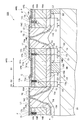
- FIG. 1 is a schematic perspective view showing a photodetecting device according to the present embodiment.
- FIG. 2 is a schematic plan view of the semiconductor photodetecting element.
- FIG. 3 is a schematic enlarged view of the semiconductor photodetector element.
- FIG. 4 is a diagram for explaining a cross-sectional configuration along the line IV-IV shown in FIG.
- the photodetection device 1 includes a semiconductor photodetection element 10A, a mounting substrate 20, and a glass substrate 30, as shown in FIG.
- the mounting substrate 20 faces the semiconductor photodetecting element 10A.
- the glass substrate 30 faces the semiconductor photodetecting element 10A.
- the semiconductor photodetecting element 10 ⁇ / b> A is disposed between the mounting substrate 20 and the glass substrate 30.
- a plane parallel to each main surface of the semiconductor photodetecting element 10A, the mounting substrate 20, and the glass substrate 30 is an XY axis plane, and a direction orthogonal to each main surface is a Z axis direction.
- the semiconductor photodetecting element 10A has a semiconductor substrate 50A having a rectangular shape in plan view.
- the semiconductor substrate 50A is made of Si and is an N-type (second conductivity type) semiconductor substrate.
- the semiconductor substrate 50A includes a main surface 1Na and a main surface 1Nb facing each other.
- the semiconductor photodetector element 10A includes a plurality of avalanche photodiodes APD and a plurality of through electrodes TE.
- the plurality of avalanche photodiodes APD are two-dimensionally arranged on the semiconductor substrate 50A.
- the plurality of avalanche photodiodes APD are arranged in a matrix.
- the row direction is the X-axis direction
- the column direction is the Y-axis direction.
- the avalanche photodiodes APD are arranged at equal intervals on a straight line when viewed from the X-axis direction and the Y-axis direction.
- Each avalanche photodiode APD has a light receiving region S1 and operates in Geiger mode.
- the light receiving region S1 is disposed on the main surface 1Na side of the semiconductor substrate 50A.
- each avalanche photodiode APD is connected in parallel with the quenching resistor R1 connected in series.
- a reverse bias voltage is applied from each power source to each avalanche photodiode APD.
- the output current from each avalanche photodiode APD is detected by the signal processing unit SP.
- the light receiving region S1 is a charge generation region (photosensitive region) where charge is generated according to incident light. That is, the light receiving area S1 is a light detection area.
- the glass substrate 30 has a main surface 30a and a main surface 30b facing each other.
- the glass substrate 30 has a rectangular shape in plan view.
- Main surface 30b is opposed to main surface 1Na of semiconductor substrate 50A.
- the main surface 30a and the main surface 30b are flat.
- the glass substrate 30 and the semiconductor photodetecting element 10A are optically connected by an optical adhesive OA.
- the glass substrate 30 may be directly formed on the semiconductor photodetecting element 10A.
- a scintillator (not shown) may be optically connected to the main surface 30a of the glass substrate 30.
- the scintillator is connected to the main surface 30a by an optical adhesive.
- the scintillation light from the scintillator passes through the glass substrate 30 and enters the semiconductor photodetecting element 10A.
- the mounting substrate 20 has a main surface 20a and a main surface 20b facing each other.
- the mounting substrate 20 has a rectangular shape in plan view.
- Main surface 20a is opposed to main surface 1Nb of semiconductor substrate 50A.
- the mounting substrate 20 includes a plurality of electrodes arranged on the main surface 20a. These electrodes are arranged corresponding to the through electrodes TE.
- the side surface 1Nc of the semiconductor substrate 50A, the side surface 30c of the glass substrate 30, and the side surface 20c of the mounting substrate 20 are flush with each other. That is, the outer edge of the semiconductor substrate 50 ⁇ / b> A, the outer edge of the glass substrate 30, and the outer edge of the mounting substrate 20 coincide with each other in plan view.
- the outer edge of the semiconductor substrate 50 ⁇ / b> A, the outer edge of the glass substrate 30, and the outer edge of the mounting substrate 20 may not coincide with each other.
- the area of the mounting substrate 20 may be larger than the areas of the semiconductor substrate 50A and the glass substrate 30 in plan view.
- the side surface 20c of the mounting substrate 20 is located outside the side surface 1Nc of the semiconductor substrate 50A and the side surface 30c of the glass substrate 30 in the XY axis plane direction.
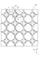
- FIG. 2 is a view of the semiconductor photodetector 10A as viewed from a direction (Z-axis direction) orthogonal to the main surface 1Na of the semiconductor substrate 50A.
- FIG. 3 shows a region where a groove is formed.
- One avalanche photodiode APD constitutes one cell in the semiconductor photodetecting element 10A.
- Each of the avalanche photodiodes APD has one light receiving region S1. That is, the semiconductor photodetecting element 10A has a plurality of light receiving regions S1.
- the light receiving region S1 has a polygonal shape when viewed from the Z-axis direction.
- the light receiving region S1 of the semiconductor photodetecting element 10A has a substantially regular octagonal shape when viewed from the Z-axis direction.
- the plurality of light receiving areas S1 are two-dimensionally arranged as viewed from the Z-axis direction.
- the plurality of light receiving regions S1 are arranged in a matrix.
- the light receiving regions S1 are arranged at equal intervals on a straight line when viewed from the X axis direction and the Y axis direction.
- the light receiving regions S1 are arranged at a pitch of 100 ⁇ m.
- two adjacent light receiving regions S1 are arranged so that one side of the octagonal shape faces each other.
- Each avalanche photodiode APD has an electrode E1.
- the electrode E1 is disposed on the main surface 1Na of the semiconductor substrate 50A.
- the electrode E1 is provided along the outline of the light receiving region S1, and has an octagonal ring shape.
- the electrode E1 has a connection portion C that is electrically connected to the light receiving region S1.
- the connection part C is provided on the four sides of the light receiving region S1.
- the connecting portions C are provided every other side of the light receiving region S1. In this case, the detection accuracy of the signal from the light receiving region S1 is ensured.
- the connection portion C includes a first end portion E1a and a second end portion E1b, and extends from the outer edge side of the light receiving region S1 toward the center side on the XY axis plane. ing.
- the electrode E1 extends in the Z-axis direction at the second end E1b. For this reason, a step is formed in the electrode E1 at the position of the second end E1b.
- the electrode E1 extends in the direction opposite to the center of the light receiving region S1 from the above-described step.
- the electrode E1 includes a third end E1c that is electrically connected to the wiring F.
- the wiring F extends from the third end E1c in the direction opposite to the center of the light receiving region S1.
- the wiring F electrically connects the electrode E1 and the electrode pad 12.
- the wiring F is located on the semiconductor substrate 50A outside the light receiving region S1.
- the wiring F is formed on the semiconductor substrate 50A via the insulating layer L1.
- the electrode E1 and the through electrode TE are made of metal.
- the electrode E1 and the through electrode TE are made of, for example, aluminum (Al).
- Al aluminum
- Cu copper
- the electrode E1 and the through electrode TE may be integrally formed.
- the electrode E1 and the through electrode TE are formed by, for example, a sputtering method.
- the semiconductor photodetecting element 10 ⁇ / b> A includes a plurality of through electrodes TE and a plurality of electrode pads 12. Each through electrode TE is electrically connected to the corresponding avalanche photodiode APD. Each electrode pad 12 is electrically connected to the corresponding through electrode TE. The electrode pad 12 is electrically connected to the electrode E1 through the wiring F. Electrode pad 12 is arranged on main surface 1Na. Each through electrode TE is electrically connected to the light receiving region S1 through the electrode pad 12, the wiring F, and the electrode E1. The electrode pad 12 is located in a region (inner region of the groove 13) AR1 surrounded by the groove 13 as viewed from the Z-axis direction, and is separated from the groove 13.
- the through electrode TE is disposed for each avalanche photodiode APD.
- the through electrode TE penetrates the semiconductor substrate 50A from the main surface 1Na side to the main surface 1Nb side.
- the through electrode TE is disposed in the through hole TH that penetrates the semiconductor substrate 50A in the thickness direction (Z-axis direction).
- the through hole TH is located in a region where a plurality of avalanche photodiodes APD are two-dimensionally arranged.
- a plurality of through holes TH are formed in the semiconductor substrate 50A.
- the opening of the through hole TH is located in the XY axis plane and has a circular shape when viewed from the Z axis direction.
- the cross-sectional shape of the through hole TH at a cutting plane parallel to the XY axis plane is a circular shape.
- the semiconductor photodetecting element 10A includes an insulating layer L2 on the inner peripheral surface of the through hole TH.
- the through electrode TE is disposed in the through hole TH via the insulating layer L2.
- the plurality of through holes TH are arranged so that the centers of the openings are located in a matrix when viewed from the Z-axis direction.
- the row direction is the X-axis direction
- the column direction is the Y-axis direction.
- the plurality of through holes TH are arranged such that the centers of the openings are arranged at equal intervals on a straight line when viewed from the X axis direction and the Y axis direction.
- the through holes TH are arranged at a pitch of 100 ⁇ m.
- the plurality of through holes TH are formed for each region surrounded by four adjacent avalanche photodiodes APD among the plurality of avalanche photodiodes APD.
- a through electrode TE electrically connected to the light receiving region S1 of one avalanche photodiode APD among the four adjacent avalanche photodiodes APD is disposed. That is, the through electrode TE is electrically connected to the light receiving region S1 of one avalanche photodiode APD among the four avalanche photodiodes APD surrounding the through hole TH in which the through electrode TE is disposed.
- the plurality of through-holes TH and the plurality of light-receiving regions S1 are configured such that the four through-holes TH surround one light-receiving region S1 and the four light-receiving regions S1 surround one through-hole TH when viewed from the Z-axis direction. positioned.
- the through holes TH and the light receiving regions S1 are alternately arranged in a direction intersecting the X axis and the Y axis.
- the four sides of the eight sides of the light receiving region S1 are opposed to one side of the adjacent light receiving region S1, and the remaining four sides are opposed to the adjacent through hole TH.
- One through hole TH is surrounded by one side of the four light receiving regions S1 when viewed from the Z-axis direction.
- the connection portion C is provided on four sides facing the through hole TH among the eight sides of the light receiving region S1.
- the main surface 1Na of the semiconductor substrate 50A includes a light receiving region S1, an intermediate region S2, and an opening peripheral region S3.
- the opening peripheral region S3 is a region located around the opening of the through hole TH of the main surface 1Na.
- the intermediate region S2 is a region on the main surface 1Na excluding the light receiving region S1 and the aperture peripheral region S3.
- a groove 13 is formed in the intermediate region S2 between the light receiving regions S1 of the four avalanche photodiodes APD adjacent to each other and the through holes TH surrounded by the avalanche photodiodes APD.
- the groove 13 extends along the side adjacent to the through hole TH among the plurality of sides of each light receiving region S1 of the four adjacent avalanche photodiodes APD as viewed from the Z-axis direction.
- the groove 13 surrounds the entire circumference of the through hole TH when viewed from the Z-axis direction.
- the area AR1 surrounded by the groove 13 is substantially square when viewed from the Z-axis direction.
- One through hole TH is formed in one region AR1.
- a groove 14 is formed in an intermediate region S2 between two light receiving regions S1 adjacent to each other.
- the groove 14 extends along two opposite sides of two adjacent light receiving regions S1 as viewed from the Z-axis direction.
- the groove 14 connects the grooves 13 surrounding different through holes TH.
- the semiconductor photodetecting element 10 ⁇ / b> A the entire circumference of the light receiving region S ⁇ b> 1 is surrounded by the grooves 13 and 14.
- One light receiving area S1 is arranged in one area AR2.
- the area AR2 has a substantially regular octagonal shape that is the same as the shape of the light receiving area S1.
- the areas AR1 and AR2 have a polygonal shape when viewed from the Z-axis direction.
- the groove 14 extends in a straight line in a region between two adjacent light receiving regions S1.
- the groove 14 surrounding the two adjacent light receiving regions S1 is shared by the two adjacent light receiving regions S1.
- the groove 14 located in a region between two adjacent light receiving regions S1 is a groove surrounding one light receiving region S1, and is also a groove surrounding the other light receiving region S1.
- the distance ⁇ from the edge 13e of the groove 13 to the edge D2 of the through hole TH surrounded by the groove 13 is equal to the distance 13f between the edge 13f of the groove 13 and the light receiving region S1 adjacent to the through hole TH. It is longer than the distance ⁇ to the edge D1.
- the distance ⁇ is 5.5 ⁇ m, and the distance ⁇ is 7.5 ⁇ m.
- the distance ⁇ is the shortest distance from the edge 13f of the groove 13 to the edge D1 of the light receiving region S1 adjacent to the through hole TH when viewed from the Z-axis direction.
- the distance ⁇ is the shortest distance from the edge 13e of the groove 13 to the edge D2 of the through hole TH surrounded by the groove 13 when viewed from the Z-axis direction.
- FIG. 4 a cross-sectional configuration of the semiconductor photodetecting element in the present embodiment will be described.
- illustration of the glass substrate 30 and the optical adhesive OA is omitted.
- Each avalanche photodiode APD includes a light receiving region S1.
- Each avalanche photodiode APD includes a P-type (first conductivity type) first semiconductor region 1PA, an N-type (second conductivity type) second semiconductor region 1NA, an N-type third semiconductor region 1NB, and P Type fourth semiconductor region 1PB.
- the first semiconductor region 1PA is located on the main surface 1Na side of the semiconductor substrate 50A.
- the second semiconductor region 1NA is located on the main surface 1Nb side of the semiconductor substrate 50A.
- the third semiconductor region 1NB is located between the first semiconductor region 1PA and the second semiconductor region 1NA, and has an impurity concentration lower than that of the second semiconductor region 1NA.
- the fourth semiconductor region 1PB is formed in the first semiconductor region 1PA and has an impurity concentration higher than that of the first semiconductor region 1PA.
- the fourth semiconductor region 1PB is the light receiving region S1.
- Each avalanche photodiode APD is from the main surface 1Na side, P + layer are quaternary semiconductor region 1PB, P layer is the first semiconductor region 1PA, N layer a third semiconductor region 1NB, the second semiconductor region 1NA It is constructed in the order of a certain N + layer.
- the first semiconductor region 1PA is located in the intermediate region S2 when viewed from the Z-axis direction, and is located so as to surround the fourth semiconductor region 1PB (light receiving region S1). Although not shown, the first semiconductor region 1PA is also located in the intermediate region S2 between the two light receiving regions S1 adjacent to each other when viewed from the Z-axis direction.
- the intermediate region S2 of the semiconductor substrate 50A has a P layer that is the first semiconductor region 1PA, an N layer that is the third semiconductor region 1NB, and a second semiconductor from the main surface 1Na side except the portion where the grooves 13 and 14 are formed.
- the region 1NA is configured in the order of N + layers.
- the inner surface 13b of the groove 13 is formed by the same N + layer as the second semiconductor region 1NA.
- An insulating layer 13c is provided on the inner surface 13b.
- a filler 13 a is disposed in the region surrounded by the insulating layer 13 c in the groove 13.
- the filler 13a is made of, for example, a material that can be easily filled and has high light shielding properties.
- the filler 13a is made of tungsten (W).
- the inner surface of the groove 14 is formed by the same N + layer as the second semiconductor region 1NA, like the inner surface 13b.
- an insulating layer 13 c and a filler 13 a are disposed in FIG. 4, the groove 14, the insulating layer 13 c and the filler 13 a disposed in the groove 14 are not illustrated.
- the filler 13a may be made of copper or aluminum instead of tungsten.
- the depth of the grooves 13 and 14, that is, the distance from the main surface 1Na to the bottom surface of the grooves 13 and 14 in the Z-axis direction (thickness direction of the semiconductor substrate 50A) is the second semiconductor from the main surface 1Na in the Z-axis direction. It is longer than the distance to the interface between the region 1NA and the third semiconductor region 1NB and shorter than the thickness of the semiconductor substrate 50A.
- the bottom surface 13d of the groove 13 is constituted by the second semiconductor region 1NA and is located closer to the main surface 1Nb than the third semiconductor region 1NB.
- the semiconductor substrate 50A has an N-type fifth semiconductor region 1NC.
- the fifth semiconductor region 1NC is formed between the edge D2 of the through hole TH and the first semiconductor region 1PA when viewed from the Z-axis direction.
- the fifth semiconductor region 1NC is an N + layer having a higher impurity concentration than the third semiconductor region 1NB, like the second semiconductor region 1NA.
- the region where the fifth semiconductor region 1NC is formed on the main surface 1Na is the opening peripheral region S3.
- the opening peripheral region S3 of the semiconductor substrate 50A is configured from the main surface 1Na side in the order of the N + layer as the fifth semiconductor region 1NC and the N + layer as the second semiconductor region 1NA.
- the inner peripheral surface (edge D2) of the through-hole TH is configured in order of the fifth semiconductor region 1NC and the second semiconductor region 1NA from the main surface 1Na side. Therefore, the PN junction formed by the first semiconductor region 1PA and the third semiconductor region 1NB is not exposed to the through hole TH.
- the avalanche photodiode APD has an electrode E1.
- the connection portion C of the electrode E1 is connected to the fourth semiconductor region 1PB (light receiving region S1). As described above, the connection portion C includes the first end portion E1a and the second end portion E1b.
- the electrode E1 includes a third end E1c.
- the first semiconductor region 1PA is electrically connected to the electrode E1 through the fourth semiconductor region 1PB.
- the electrode pad 12 is electrically connected to the through electrode TE.
- the through electrode TE extends to the back surface side (main surface 1Nb side) of the semiconductor substrate 50A.
- an insulating layer L3 is provided on the mounting substrate 20 side.
- the through electrode TE is electrically connected to the mounting substrate 20 through the bump electrode BE on the back surface side of the semiconductor substrate 50A.
- the electrode E1 and the mounting substrate 20 are electrically connected through the wiring F, the electrode pad 12, the through electrode TE, and the bump electrode BE.
- the fourth semiconductor region 1PB is electrically connected to the mounting substrate 20 through the electrode E1, the wiring F, the electrode pad 12, the through electrode TE, and the bump electrode BE.
- the bump electrode BE is made of, for example, solder.
- the bump electrode BE is formed on the through electrode TE extending on the main surface 1Nb via an unillustrated UBM (Under Bump Metal).
- the UBM is made of a material that is electrically and physically connected to the bump electrode BE.
- the UBM is formed by, for example, an electroless plating method.
- the bump electrode BE is formed by, for example, a method of mounting a solder ball or a printing method.
- FIG. 5 is a schematic plan view of the mounting substrate.
- the mounting substrate 20 includes a plurality of electrodes E9, a plurality of quenching resistors R1, and a plurality of signal processing units SP.
- the mounting board 20 constitutes an ASIC (Application Specific Integrated Circuit).
- the quenching resistor R1 may be arranged not on the mounting substrate 20 but on the semiconductor photodetecting element 10A.
- Each electrode E9 is electrically connected to the bump electrode BE. Similarly to the electrode E1 and the through electrode TE, the electrode E9 is made of metal.
- the electrode E9 is made of, for example, aluminum.
- the material constituting the electrode E9 may be copper other than aluminum.
- Each quenching resistor R1 is arranged on the main surface 20a side. One end of the quenching resistor R1 is electrically connected to the electrode E9, and the other end of the quenching resistor R1 is connected to the common electrode CE.
- the quenching resistor R1 constitutes a passive quenching circuit. A plurality of quenching resistors R1 are connected in parallel to the common electrode CE.
- Each signal processing unit SP is arranged on the main surface 20a side. The input end of the signal processing unit SP is electrically connected to the electrode E9, and the output end of the signal processing unit SP is connected to the signal line TL. An output signal from the corresponding avalanche photodiode APD (semiconductor photodetecting element 10A) is input to each signal processing unit SP through the electrode E1, the through electrode TE, the bump electrode BE, and the electrode E9. Each signal processing unit SP processes an output signal from the corresponding avalanche photodiode APD. Each signal processing unit SP includes a CMOS circuit that converts an output signal from the corresponding avalanche photodiode APD into a digital pulse.
- CMOS circuit that converts an output signal from the corresponding avalanche photodiode APD into a digital pulse.
- FIG. 6 is a circuit diagram of the photodetector.
- an avalanche photodiode APD is formed by a PN junction formed between the N-type third semiconductor region 1NB and the P-type first semiconductor region 1PA. Yes.
- the semiconductor substrate 50A is electrically connected to an electrode (not shown) arranged on the back side, and the first semiconductor region 1PA is connected to the electrode E1 through the fourth semiconductor region 1PB.
- Each quenching resistor R1 is connected in series with a corresponding avalanche photodiode APD.
- each avalanche photodiode APD operates in Geiger mode.
- a reverse voltage (reverse bias voltage) larger than the breakdown voltage of the avalanche photodiode APD is applied between the anode and the cathode of the avalanche photodiode APD.
- the ( ⁇ ) potential V1 is applied to the anode
- the (+) potential V2 is applied to the cathode.
- the polarities of these potentials are relative, and one potential may be a ground potential.
- the anode is the first semiconductor region 1PA, and the cathode is the third semiconductor region 1NB.
- photoelectric conversion is performed inside the substrate to generate photoelectrons.
- Avalanche multiplication is performed in a region near the PN junction interface of the first semiconductor region 1PA, and the amplified electron group travels toward an electrode disposed on the back surface side of the semiconductor substrate 50A.
- light (photon) enters one of the cells (avalanche photodiode APD) of the semiconductor photodetecting element 10A it is multiplied and taken out from the electrode E9 as a signal.
- the signal extracted from the electrode E9 is input to the corresponding signal processing unit SP.
- the groove 13 surrounding the through hole TH on the main surface 1Na side of the semiconductor substrate 50A is an intermediate between the through hole TH and the light receiving region S1 adjacent to the through hole TH. It is formed in region S2. For this reason, the main surface 1Na of the semiconductor substrate 50A is divided in the intermediate region S2 between the through electrode TE and the light receiving region S1. As a result, even when the light receiving region S1 and the through electrode TE are close to each other in order to ensure the aperture ratio of the avalanche photodiode APD, the flow of surface leakage current from the through electrode TE to the avalanche photodiode APD is reduced. .
- the distance ⁇ is longer than the distance ⁇ . For this reason, a structural defect hardly occurs around the through hole TH in the semiconductor substrate 50A.
- the bottom surface 13d of the groove 13 is constituted by the second semiconductor region 1NA.
- the bottom surface 13d of the groove 13 is deeper than the third semiconductor region 1NB. For this reason, when a charge is generated in a region surrounded by the groove 13 in the semiconductor substrate 50A, the charge generated in the region is suppressed from moving to the avalanche photodiode APD. Since the bottom surface 13d of the groove 13 is formed in the semiconductor substrate 50A, that is, the groove 13 does not reach the main surface 1Nb of the semiconductor substrate 50A, there is no possibility that the semiconductor substrate 50A is separated at the position of the groove 13. Therefore, in the manufacturing process of the photodetecting device 1, the semiconductor substrate 50A can be easily handled.
- a filler 13a made of tungsten is arranged in the groove 13. Since the electrode pad 12 is separated from the groove 13, the parasitic capacitance generated between the electrode pad 12 and the filler 13a is reduced.
- the region AR1 and the region AR2 When viewed from the Z-axis direction, the region AR1 and the region AR2 have a polygonal shape, and the light receiving region S1 has a polygonal shape.
- the light receiving region S1 When the light receiving region S1 is circular, there is no corner where the electric field concentrates.
- the light receiving region S1 has a circular shape, the dead space generated between the light receiving region S1 and the through hole TH is larger than when the light receiving region S1 has a polygonal shape.
- the areas AR1 and AR2 and the light receiving area S1 are polygonal shapes.
- the regions AR1, AR2 and the light receiving region S1 are arranged so that the sides of the regions AR1, AR2 and the side of the light receiving region S1 are along. For this reason, in the photodetection device 1, the dead space is small and the aperture ratio is large.
- the opening of the through hole TH has a circular shape, and the insulating layer L2 is disposed on the inner peripheral surface of the through hole TH.
- the through electrode TE and the semiconductor substrate 50A are electrically insulated. If corners exist in the openings of the through holes TH, when the insulating layer L2 is formed, the insulating layer L2 formed at the corners may be cracked.
- the through hole TH since the through hole TH has a circular shape when viewed from the direction orthogonal to the main surface 1Na, the insulating layer L2 is unlikely to crack when the insulating layer L2 is formed. Therefore, in the photodetector 1, electrical insulation between the through electrode TE and the semiconductor substrate 50A is ensured.
- the through electrode TE is electrically connected to the light receiving region S1 of one avalanche photodiode APD among the four adjacent avalanche photodiodes APD.
- the wiring distance between the through electrode TE and the light receiving region S1 electrically connected to the through electrode TE is relatively short, the wiring resistance and the parasitic capacitance are hardly affected. Therefore, deterioration of detection accuracy in the light detection device 1 is suppressed.
- the light receiving region S1 has a polygonal shape when viewed from the Z-axis direction.
- the groove 13 extends along the side adjacent to the through hole TH among the plurality of sides of each of the light receiving regions S1 of the four avalanche photodiodes APD adjacent to the through hole TH when viewed from the Z-axis direction. Yes. Since the groove 13 extends along the side of the light receiving region S1, even when the through hole TH is formed in each region surrounded by four adjacent avalanche photodiodes APD, It is possible to set the interval with the region S1 narrow. Therefore, in the photodetecting device 1, the dead space is small and the aperture ratio is large.
- the light receiving region S1 has an octagonal shape when viewed from the Z-axis direction, it is possible to effectively utilize a region other than the through electrode TE in the main surface 1Na. Accordingly, in the light detection device 1, a configuration in which the wiring distance between the through electrode TE and the light receiving region S1 is short is realized, and the aperture ratio is higher than that in the case where the light receiving region S1 has another shape. improves.
- the filler 13a disposed in the grooves 13 and 14 is made of metal, a parasitic capacitance may be generated between the filler 13a and the light receiving region S1. If the value of the parasitic capacitance differs depending on the position between the filler 13a and the light receiving region S1, that is, if the parasitic capacitance value is biased, the light detection accuracy of the avalanche photodiode APD decreases. There is a fear.
- the grooves 13 and 14 are formed so that the edges of the grooves 13 and 14 are along the edge D1 of the light receiving region S1 when viewed from the Z-axis direction.
- the groove 14 surrounding two adjacent light receiving regions S1 is formed so that the edge of the groove 14 is along the edge D1 of the light receiving region S1.
- the groove 14 is shared by two adjacent light receiving regions S1. For this reason, the influence of the parasitic capacitance on the avalanche photodiode APD is reduced. Further, since the area of the main surface 1Na is effectively used, the light receiving areas S1 of the avalanche photodiodes APD are densely arranged. As a result, both reduction of the influence of parasitic capacitance on the avalanche photodiode APD and improvement of the aperture ratio are compatible.
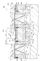
- FIG. 7 is a diagram for explaining a cross-sectional configuration of a photodetection device according to a modification of the present embodiment.
- FIG. 7 shows a cross-sectional configuration when the photodetecting device according to the present modification is cut along a plane corresponding to line IV-IV shown in FIG. Also in FIG. 7, illustration of the glass substrate 30 and the optical adhesive OA is omitted.
- This modification is generally similar to or the same as the above-described embodiment, but as described below, this modification is different from the above-described embodiment with respect to the configuration of the avalanche photodiode APD.
- the light detection device includes a semiconductor light detection element 10B.
- the semiconductor photodetecting element 10 ⁇ / b> B is disposed between the mounting substrate 20 and the glass substrate 30.
- the semiconductor photodetecting element 10B has a semiconductor substrate 50B that has a rectangular shape in plan view.
- the semiconductor substrate 50B is made of Si and is an N-type (second conductivity type) semiconductor substrate.
- Semiconductor substrate 50B includes a main surface 1Na and a main surface 1Nb facing each other.
- the semiconductor photodetecting element 10B includes a plurality of avalanche photodiodes APD and a plurality of through electrodes TE.
- the plurality of avalanche photodiodes APD are two-dimensionally arranged on the semiconductor substrate 50B. In this modification, the plurality of avalanche photodiodes APD are arranged in a matrix.
- the groove 23 formed in the semiconductor light detection element 10B has the same configuration as the groove 13 formed in the semiconductor light detection element 10A.
- the groove 23 is formed in an intermediate region S2 between the light receiving regions S1 of the four adjacent avalanche photodiodes APD and the through holes TH surrounded by the avalanche photodiodes APD.
- the groove 23 extends along the side adjacent to the through hole TH among the plurality of sides of each light receiving region S1 of the four avalanche photodiodes APD adjacent to the through hole TH when viewed from the Z-axis direction. .
- the groove 23 surrounds the entire circumference of the through hole TH.
- the area AR1 surrounded by the groove 23 is substantially square when viewed from the Z-axis direction.
- one through hole TH is formed in one region AR1.
- a groove 14 is formed in an intermediate region S2 between two light receiving regions S1 adjacent to each other. In FIG. 7, the groove 14 is not shown. The groove 14 extends along two opposite sides of two adjacent light receiving regions S1 when viewed from the Z direction. The groove 14 connects the grooves 23 surrounding different through holes TH. Also in the semiconductor light detection element 10B, the entire circumference of the light receiving region S1 is surrounded by the grooves 23 and 14. The area AR2 surrounded by the grooves 23 and 14 has a substantially regular octagonal shape that is the same as the shape of the light receiving area S1. Also in this modification, the areas AR1 and AR2 have a polygonal shape when viewed from the Z-axis direction. One light receiving area S1 is arranged in one area AR2.
- the groove 14 extends in a straight line in a region between two adjacent light receiving regions S1.
- the groove 14 surrounding the two adjacent light receiving regions S1 is shared by the two adjacent light receiving regions S1.
- the distance ⁇ from the edge 23e of the groove 23 to the edge D2 of the through hole TH surrounded by the groove 23 is the edge of the light receiving region S1 adjacent to the through hole TH from the edge 23f of the groove 23. It is longer than the distance ⁇ to D1.
- the distance ⁇ is 5.5 ⁇ m and the distance ⁇ is 7.5 ⁇ m.
- the distance ⁇ is the shortest distance from the edge 23f of the groove 23 to the edge D1 of the light receiving region S1 adjacent to the through hole TH when viewed from the Z-axis direction.
- the distance ⁇ is the shortest distance from the edge 23e of the groove 23 to the edge D2 of the through hole TH surrounded by the groove 23 when viewed from the Z-axis direction.
- each avalanche photodiode APD includes a light receiving region S1.
- Each avalanche photodiode APD includes a P-type (first conductivity type) first semiconductor region 2PA, a P-type second semiconductor region 2PB, an N-type third semiconductor region 2NA, and a P-type fourth semiconductor region. 2PC.
- the first semiconductor region 2PA is located on the main surface 1Na side of the semiconductor substrate 50B.
- the second semiconductor region 2PB is located on the main surface 1Nb side of the semiconductor substrate 50B and has a higher impurity concentration than the first semiconductor region 2PA.
- the third semiconductor region 2NA is formed on the main surface 1Na side of the first semiconductor region 2PA.
- the fourth semiconductor region 2PC is formed in the first semiconductor region 2PA so as to be in contact with the third semiconductor region 2NA, and has an impurity concentration higher than that of the first semiconductor region 2PA.
- the third semiconductor region 2NA is the light receiving region S1.
- Each avalanche photodiode APD is from the main surface 1Na side, N + layer a third semiconductor region 2NA, P layer are quaternary semiconductor region 2PC, a first semiconductor region 2PA P - layer, the second semiconductor region 2PB In the order of the P + layers.
- the first semiconductor region 2PA is located in the intermediate region S2 when viewed from the Z-axis direction, and is located so as to surround the third semiconductor region 2NA that is the light receiving region S1. Although not shown, the first semiconductor region 2PA is also located in the intermediate region S2 between the two light receiving regions S1 adjacent to each other when viewed from the Z-axis direction.
- the intermediate region S2 of the semiconductor substrate 50B is in the order of the P ⁇ layer that is the first semiconductor region 2PA and the P + layer that is the second semiconductor region 2PB from the main surface 1Na side except the portion where the grooves 23 and 14 are formed. It consists of
- the inner surface 23b of the groove 23 is formed by the same P + layer as that of the second semiconductor region 2PB.
- An insulating layer 23c is provided on the inner surface 23b.
- a filler 23a is disposed in the region surrounded by the insulating layer 23c in the groove 23.
- the filler 23a is made of, for example, a material that can be easily filled and has high light shielding properties.
- the filler 23a is made of tungsten (W), like the filler 13a.
- the inner surface of the groove 14 is formed by a P + layer having a higher impurity concentration than the first semiconductor region 2PA.
- an insulating layer 23 c and a filler 23 a are disposed in the groove 14. In FIG. 7, as described above, the groove 14 and the insulating layer 23c and the filler 23a disposed in the groove 14 are not illustrated.
- the filler 13a may be made of copper or aluminum instead of tungsten.
- the depth of the grooves 23, 14, that is, the distance from the main surface 1 Na in the Z-axis direction (the thickness direction of the semiconductor substrate 50 B) to the bottom surfaces of the grooves 23, 14 is the main surface 1 Na in the Z-axis direction to the first semiconductor. It is longer than the distance to the interface between the region 2PA and the second semiconductor region 2PB and shorter than the thickness of the semiconductor substrate 50B.
- the bottom surface 23d of the groove 23 is configured by the second semiconductor region 2PB, and is located closer to the main surface 1Nb than the first semiconductor region 2PA.
- the semiconductor substrate 50B has a P-type fifth semiconductor region 2PD.
- the fifth semiconductor region 2PD is formed between the edge D2 of the through hole TH and the first semiconductor region 2PA when viewed from the Z-axis direction.
- the fifth semiconductor region 2PD is a P + layer having a higher impurity concentration than the first semiconductor region 2PA, like the second semiconductor region 2PB.
- a region where the fifth semiconductor region 2PD is formed in the main surface 1Na is the opening peripheral region S3.
- the opening peripheral region S3 of the semiconductor substrate 50B is configured from the main surface 1Na side in the order of the P + layer that is the fifth semiconductor region 2PD and the P + layer that is the second semiconductor region 2PB.
- the inner peripheral surface (edge D2) of the through hole TH is configured in order of the fifth semiconductor region 2PD and the second semiconductor region 2PB from the main surface 1Na side. Therefore, the PN junction formed by the third semiconductor region 2NA and the fourth semiconductor region 2PC is not exposed to the through hole TH.
- the avalanche photodiode APD has an electrode E1.
- the electrode E1 is disposed on the main surface 1Na side of the semiconductor substrate 50B. Also in this modification, the electrode E1 is provided along the outline of the light receiving region S1 and has an octagonal ring shape.
- the electrode E1 has a connection portion C that is electrically connected to the light receiving region S1. Also in this modification, as FIG. 7 shows, the connection part C contains the 1st end part E1a and the 2nd end part E1b. The electrode E1 includes a third end E1c that is electrically connected to the wiring F.
- the wiring F extends from the third end E1c in the direction opposite to the center of the light receiving region S1.
- the wiring F electrically connects the electrode E1 and the electrode pad 12.
- the wiring F is located on the semiconductor substrate 50B outside the light receiving region S1.
- the wiring F is formed on the semiconductor substrate 50B via the insulating layer L1.
- the electrode pad 12 is electrically connected to the through electrode TE.
- the through electrode TE extends to the back surface side (main surface 1Nb side) of the semiconductor substrate 50B.
- the through electrode TE is provided with an insulating layer L3.
- the through electrode TE is electrically connected to the mounting substrate 20 by the bump electrode BE.
- the electrode E1 and the mounting substrate 20 are electrically connected through the wiring F, the electrode pad 12, the through electrode TE, and the bump electrode BE.
- the third semiconductor region 2NA is electrically connected to the mounting substrate 20 through the electrode E1, the wiring F, the electrode pad 12, the through electrode TE, and the bump electrode BE.
- the groove 23 surrounding the through hole TH on the main surface 1Na side of the semiconductor substrate 50B is an intermediate between the through hole TH and the light receiving region S1 adjacent to the through hole TH. It is formed in region S2. For this reason, the main surface 1Na of the semiconductor substrate 50B is divided in the intermediate region S2 between the through electrode TE and the light receiving region S1. As a result, even when the light receiving region S1 and the through electrode TE are close to each other in order to ensure the aperture ratio of the avalanche photodiode APD, the flow of surface leakage current from the through electrode TE to the avalanche photodiode APD is reduced. .
- the distance ⁇ is longer than the distance ⁇ . For this reason, a structural defect hardly occurs around the through hole TH in the semiconductor substrate 50B.
- the bottom surface 23d of the groove 23 is constituted by the second semiconductor region 2PB.
- the bottom surface 23d of the groove 23 is deeper than the first semiconductor region 2PA. For this reason, when a charge is generated in a region surrounded by the groove 23 in the semiconductor substrate 50B, the charge generated in the region is suppressed from moving to the avalanche photodiode APD. Since the bottom surface 23d of the groove 23 is formed in the semiconductor substrate 50B, that is, the groove 23 does not reach the main surface 1Nb of the semiconductor substrate 50B, there is no possibility that the semiconductor substrate 50B is separated at the position of the groove 23. Therefore, it is easy to handle the semiconductor substrate 50B even in the manufacturing process of the photodetector according to this modification.
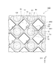
- FIGS. 8 to 11 are schematic plan views showing modified examples of the semiconductor photodetecting element.
- the semiconductor photodetecting elements 10C, 10D, 10E, and 10F are disposed between the mounting substrate 20 and the glass substrate 30.
- the semiconductor photodetecting elements 10C, 10D, 10E, and 10F have a semiconductor substrate 50A that has a rectangular shape in plan view, like the semiconductor photodetecting element 10A.
- the semiconductor photodetecting elements 10C, 10D, 10E, and 10F include a plurality of avalanche photodiodes APD and a plurality of through electrodes TE.
- a groove 13 is formed in an intermediate region S2 between the through hole TH and the light receiving region S1 adjacent to the through hole TH.
- the groove 13 surrounds the through hole TH.
- the groove 13 is not formed in a region where the wiring F that electrically connects the through electrode TE and the light receiving region S1 is disposed as viewed from the Z-axis direction.
- the groove 13 surrounds the through hole TH in a state where the groove 13 is divided in a region where the wiring F is disposed as viewed from the Z-axis direction.
- a groove 13 is formed in an intermediate region S2 between the through hole TH and the light receiving region S1 adjacent to the through hole TH.
- the groove 13 surrounds the through hole TH.
- FIG. 2 and FIG. 9 are different in scale.
- the size of the electrode pad 12 of the semiconductor photodetecting element 10D is the same as the size of the electrode pad 12 of the semiconductor photodetecting element 10A.
- the through holes TH and the light receiving areas S1 are two-dimensionally arranged. Each pitch of the through hole TH and the light receiving region S1 is smaller than that of the semiconductor photodetector 10A. In the semiconductor photodetector 10D, the through holes TH and the light receiving regions S1 are arranged in a one-to-one relationship so that the resolution is higher than that of the semiconductor photodetector 10A. Each pitch of the light receiving region S1 and the through holes TH is, for example, 70 ⁇ m.
- the groove 13 surrounds the through hole TH, similarly to the semiconductor photodetecting element 10A.
- the groove 14 also extends along two opposite sides of the two adjacent light receiving regions S1 when viewed from the Z-axis direction.
- the groove 14 connects the grooves 13 surrounding different through holes TH.
- the entire circumference of the light receiving region S1 is surrounded by the grooves 13 and 14.
- each pitch of the through electrode TE and the light receiving region S1 is smaller than that of the semiconductor photodetecting element 10A.
- the groove 14 surrounding the two adjacent light receiving regions S1 is formed so that the edge of the groove 14 is along the edge D1 of the light receiving region S1. .
- the groove 14 is shared by two adjacent light receiving regions S1. For this reason, the influence of the parasitic capacitance on the avalanche photodiode APD is reduced. Further, since the area of the main surface 1Na is effectively used, the light receiving areas S1 of the avalanche photodiodes APD are densely arranged.
- the light receiving region S1 has a polygonal shape.
- the light receiving region S1 of the semiconductor light detecting element 10D has a polygonal shape different from that of the light receiving region S1 of the semiconductor light detecting element 10A. Specifically, the light receiving region S1 of the semiconductor photodetector 10D has a polygonal shape in which the length of the side facing the adjacent light receiving region S1 is shorter than the length of the side facing the adjacent through hole TH. Yes.
- the semiconductor light detection element 10D has a higher resolution and a higher aperture ratio than the semiconductor light detection element 10A. Parasitic capacitance generated among the avalanche photodiode APD, the filler 13a, and the electrode pad 12 is reduced.
- a groove 13 is formed in an intermediate region S2 between the through hole TH and the light receiving region S1 adjacent to the through hole TH.
- the groove 13 surrounds the through hole TH. 2 and FIG. 10 are different in scale.
- the size of the electrode pad 12 of the semiconductor photodetecting element 10E is the same as the size of the electrode pad 12 of the semiconductor photodetecting element 10A.
- the pitch of the through holes TH is the same as the pitch of the through holes TH of the semiconductor photodetector 10A
- the pitch of the light receiving regions S1 is the same as the pitch of the light receiving regions S1 of the semiconductor photodetector 10A.
- the through hole TH and the light receiving region S1 are arranged in a one-to-one relationship between the through hole TH and the light receiving region S1.
- the light receiving region S1 of the semiconductor light detecting element 10E has a substantially octagonal shape, similar to the light receiving region S1 of the semiconductor light detecting element 10A.
- the area of the light receiving region S1 of the semiconductor photodetector 10E is smaller than the area of the light receiving region S1 of the semiconductor photodetector 10A.
- two grooves 14 extend in a region between two light receiving regions S1 adjacent to each other.
- One groove 14 surrounds one light receiving region S1, and the other groove 14 surrounds the other light receiving region S1. That is, the groove 14 is not shared for two adjacent light receiving regions S1.
- the groove 13 of the semiconductor photodetecting element 10E surrounds the through hole TH in a state of being divided in the row direction and the column direction in which the through holes TH are arranged. Similar to the groove 14 of the semiconductor light detection element 10A, the groove 14 of the semiconductor light detection element 10E extends along opposite sides of the two adjacent light receiving regions S1 when viewed from the Z-axis direction. The groove 14 connects the grooves 13 surrounding different through holes TH. In the semiconductor photodetecting element 10E, the entire circumference of the light receiving region S1 is surrounded by the grooves 13 and 14.
- the grooves 13 and 14 are formed so that the edges of the grooves 13 and 14 are along the edge D1 of the light receiving region S1. It is difficult to reduce the size of the through electrode TE in order to ensure processing accuracy or ensure electrical connection. In order to reduce the parasitic capacitance generated between the electrode pad 12 and the filler 13 a disposed in the grooves 13 and 14, the grooves 13 and 14 are separated from the electrode pad 12.
- the semiconductor photodetecting element 10E since the two grooves 14 extend in the area between the two light receiving areas S1 adjacent to each other, the crosstalk between the light receiving areas S1 is reduced as compared with the semiconductor photodetecting element 10A. The Therefore, in the semiconductor photodetecting element 10E, the crosstalk between the light receiving regions S1 is reduced as compared with the semiconductor photodetecting element 10A, and the parasitic capacitance generated between the avalanche photodiode APD, the filler 13a, and the electrode pad 12 is reduced. Reduced.
- a groove 13 is formed in an intermediate region S2 between the through hole TH and the light receiving region S1 adjacent to the through hole TH.
- the groove 13 surrounds the through hole TH.
- FIG. 10 and FIG. 11 are different in scale.
- the size of the electrode pad 12 of the semiconductor photodetecting element 10F is the same as the size of the electrode pad 12 of the semiconductor photodetecting element 10E.
- the through holes TH and the light receiving areas S1 are two-dimensionally arranged. Each pitch of the through hole TH and the light receiving region S1 is smaller than that of the semiconductor photodetector 10E.
- the through holes TH and the light receiving regions S1 are arranged in a one-to-one relationship so that the resolution is higher than that of the semiconductor light detection element 10E.
- Each pitch of the light receiving region S1 and the through holes TH is, for example, 50 ⁇ m.
- the groove 13 of the semiconductor photodetecting element 10F surrounds the through hole TH in a state of being divided in the row direction and the column direction in which the through holes TH are arranged. Similar to the groove 14 of the semiconductor light detection element 10E, the groove 14 of the semiconductor light detection element 10F extends along the mutually opposing sides of the two adjacent light receiving regions S1 as viewed from the Z-axis direction. The groove 14 connects the grooves 13 surrounding different through holes TH. In the semiconductor photodetecting element 10F, the entire circumference of the light receiving region S1 is surrounded by the grooves 13 and 14.
- the grooves 13 and 14 are formed so that the edges of the grooves 13 and 14 are along the edge D1 of the light receiving region S1. It is difficult to reduce the size of the through electrode TE in order to ensure processing accuracy or ensure electrical connection. In order to reduce the parasitic capacitance generated between the electrode pad 12 and the filler 13 a disposed in the grooves 13 and 14, the grooves 13 and 14 are separated from the electrode pad 12.
- the groove 14 is not shared by two adjacent light receiving regions S1, and the light receiving region S1 of the semiconductor photodetector 10F has a shape different from that of the light receiving region S1 of the semiconductor photodetector 10E. It has a polygonal shape. Specifically, the light receiving region S1 of the semiconductor photodetector 10F has a polygonal shape in which the length of the side facing the adjacent light receiving region S1 is shorter than the length of the side facing the adjacent through hole TH. Yes.
- the semiconductor photodetecting element 10F has higher resolution than the semiconductor photodetecting element 10E, and an aperture ratio is ensured. Parasitic capacitance generated among the avalanche photodiode APD, the filler 13a, and the electrode pad 12 is reduced.
- one avalanche photodiode APD is electrically connected to one through electrode TE (one electrode pad 12), but the present invention is not limited to this.
- a plurality of avalanche photodiodes APD may be electrically connected to one through electrode TE (one electrode pad 12).
- the two-layer structure of the semiconductor substrate 50A and the semiconductor substrate 50B is shown for the avalanche photodiode APD, but the layer structure of the semiconductor substrate is not limited to these.
- the avalanche photodiode APD provided on the semiconductor substrate 50A for example, the second semiconductor region 1NA and the third semiconductor region 1NB may be configured by one semiconductor region.
- the avalanche photodiode APD includes a first conductivity type (for example, N type) semiconductor region and a second conductivity type (for example, P type) semiconductor region that forms a pn junction with the first conductivity type semiconductor region.
- the second conductivity type semiconductor region having a higher impurity concentration is the light receiving region.
- the first semiconductor region 2PA, the second semiconductor region 2PB, and the fourth semiconductor region 2PC may be configured by one semiconductor region.
- the avalanche photodiode APD is located in the first conductivity type (for example, P type) semiconductor region, the first conductivity type semiconductor region, and has a pn junction with the first conductivity type semiconductor region.
- the P-type and N-type conductivity types may be switched so as to be opposite to the above-described conductivity types.
- the light receiving region S1 of the semiconductor substrate 50A may be configured in the order of the N + layer, the N layer, the P layer, and the P + layer from the main surface 1Na side.
- the light receiving region S1 of the semiconductor substrate 50B may be configured in the order of the P + layer, the N layer, the N ⁇ layer, and the N + layer from the main surface 1Na side.
- the distance ⁇ is 5.5 ⁇ m, and the distance ⁇ is 7.5 ⁇ m.
- the distance ⁇ and the distance ⁇ may be other than the above values as long as the distance ⁇ is longer than the distance ⁇ .
- the light receiving region S1 is described as having a polygonal shape (for example, a substantially regular octagonal shape) when viewed from the Z-axis direction, but other shapes may be used. .
- the light receiving region S1 may have a circular shape or any other appropriate shape.
- the through hole TH has been described as having a circular shape when viewed from the Z-axis direction, but other shapes may be used.
- the through hole TH may have a polygonal shape or any other appropriate shape.
- the present invention can be used for a light detection device that detects weak light.
- SYMBOLS 1 Photodetection device, 12 ... Electrode pad, 13, 23 ... Groove, 13d, 23d ... Bottom, 50A, 50B ... Semiconductor substrate, 1Na, 1Nb ... Main surface, S1 ... Light receiving region, S2 ... Intermediate region, APD ... Avalanche Photodiode, TH ... through hole, TE ... through electrode, ⁇ , ⁇ ... distance, 1PA ... first semiconductor region, 1PB ... fourth semiconductor region, 1NA ... second semiconductor region, 1NB ... third semiconductor region, 2PA ... first One semiconductor region, 2PB ... second semiconductor region, 2PC ... fourth semiconductor region, 2NA ... third semiconductor region, AR1, AR2 ... region, D1, D2, 13e, 13f ... edge.
Abstract
光検出装置は、半導体基板と、半導体基板の第一主面側に配置されている受光領域を有していると共に半導体基板に二次元配列されている複数のアバランシェフォトダイオードと、対応する受光領域と電気的に接続されている貫通電極と、を備えている。貫通電極は、複数のアバランシェフォトダイオードが二次元配列されている領域内で半導体基板を貫通している貫通孔に配置されている。半導体基板の第一主面側には、貫通孔を囲んでいる溝が、貫通孔と貫通孔と隣り合う受光領域との間の領域に形成されている。溝の縁と、溝によって囲まれている貫通孔の縁との第一距離は、溝の縁と、溝によって囲まれている貫通孔と隣り合う受光領域の縁との第二距離よりも長い。
Description
本発明は、光検出装置に関する。
互いに対向する第一主面及び第二主面を含む半導体基板を有する光検出装置が知られている(たとえば、特許文献1参照)。特許文献1に記載の光検出装置は、ガイガーモードで動作する複数のアバランシェフォトダイオードと、対応するアバランシェフォトダイオードと電気的に接続されている貫通電極と、を備えている。複数のアバランシェフォトダイオードは、半導体基板に二次元配列されている。各アバランシェフォトダイオードは、半導体基板の第一主面側に配置されている受光領域を有している。貫通電極は、半導体基板を厚み方向に貫通している貫通孔に配置されている。
本発明の一態様は、開口率が確保されていると共に、アバランシェフォトダイオードへの表面リーク電流の流れ込みが低減されており、半導体基板における貫通孔の周囲に構造欠陥が生じ難い光検出装置を提供することを目的とする。
本発明者らは、調査研究の結果、以下のような事実を新たに見出した。
光検出装置が複数のアバランシェフォトダイオードを備えている場合、たとえば、アバランシェフォトダイオードからの配線距離を短くするために、貫通電極は、複数のアバランシェフォトダイオードが二次元配列されている第一領域内に配置される。貫通電極が第一領域外に配置されている場合、貫通電極が第一領域内に配置されている場合に比して、アバランシェフォトダイオードから貫通電極までの配線距離が長く、かつ、アバランシェフォトダイオード間での配線距離の差が大きい。配線距離は、配線抵抗及び寄生容量などと関連しており、光検出装置での検出精度に影響を与える。
貫通電極が配置される貫通孔は、光検出に関してデッドスペースになる。このため、貫通電極が第一領域内に配置されている場合、貫通電極が第一領域外に配置されている場合に比べて、光検出に有効な面積が小さい、すなわち、開口率が低下するおそれがある。開口率が低下すると、光検出装置の光検出特性が低下する。
開口率の低下を抑制するためには、デッドスペースは、できる限り小さいことが望ましい。たとえば、アバランシェフォトダイオードと貫通孔(貫通電極)との間隔を小さくすることにより、開口率が確保される。しかしながら、アバランシェフォトダイオードと貫通孔との間隔が小さい場合、アバランシェフォトダイオードと貫通孔との間隔が大きい場合に比して、貫通孔からアバランシェフォトダイオードに表面リーク電流が流れ込みやすい。この結果、光検出装置での検出精度に悪影響を与えるおそれがある。
そこで、本発明者らは、開口率が確保されていると共に、アバランシェフォトダイオードへの表面リーク電流の流れ込みが低減されている構成について鋭意研究を行った。
本発明者らは、半導体基板の第一主面側に、貫通孔を囲んでいる溝が、貫通孔と当該貫通孔と隣り合うアバランシェフォトダイオードの受光領域との間の領域に形成されている構成を見出した。この構成では、貫通孔を囲んでいる溝が、貫通孔と当該貫通孔と隣り合うアバランシェフォトダイオードの受光領域との間の領域に形成されているので、受光領域と貫通電極(貫通孔)との間隔が小さい場合でも、貫通孔からアバランシェフォトダイオードへの表面リーク電流の流れ込みが低減される。
本発明者らは、貫通孔を囲んでいる溝が半導体基板に形成されることによって、新たな問題点が生じることも見出した。貫通孔を囲んでいる溝は、貫通孔と受光領域との間の狭い領域に形成される。このため、半導体基板における、溝と当該溝によって囲まれている貫通孔との間の領域に、構造欠陥が生じるおそれがある。構造欠陥は、たとえば、半導体基板の割れ又は欠けなどである。溝の縁から当該溝によって囲まれている貫通孔の縁までの第一距離が、溝の縁から当該溝によって囲まれている貫通孔と隣り合う受光領域の縁までの第二距離以下である場合、第一距離が第二距離よりも長い場合に比して、構造欠陥が生じやすい。
本発明者らは、第一距離が第二距離よりも長い構成を見出した。この構成によれば、受光領域の縁と当該受光領域と隣り合う貫通孔の縁との間隔が小さく、かつ、半導体基板における、受光領域と当該受光領域と隣り合う貫通孔との間に当該貫通孔を囲んでいる溝が形成される場合でも、半導体基板における、溝と当該溝によって囲まれている貫通孔との間の領域に、構造欠陥が生じ難い。
本発明の一態様は、光検出装置であって、互いに対向する第一主面及び第二主面を有している半導体基板と、ガイガーモードで動作する複数のアバランシェフォトダイオードと、貫通電極と、を備えている。複数のアバランシェフォトダイオードは、半導体基板の第一主面側に配置されている受光領域を有していると共に、半導体基板に二次元配列されている。貫通電極は、対応する受光領域と電気的に接続されている。貫通電極は、複数のアバランシェフォトダイオードが二次元配列されている領域内で半導体基板を厚み方向に貫通している貫通孔に配置されている。半導体基板の第一主面側には、貫通孔を囲んでいる溝が、貫通孔と貫通孔と隣り合う受光領域との間の領域に形成されている。溝の縁と、溝によって囲まれている貫通孔の縁との第一距離は、溝の縁と、溝によって囲まれている貫通孔と隣り合う受光領域の縁との第二距離よりも長い。
本一態様に係る光検出装置では、半導体基板の第一主面側に、貫通孔を囲んでいる溝が、貫通孔と貫通孔と隣り合う受光領域との間の領域に形成されているので、開口率が確保されていると共に、アバランシェフォトダイオードへの表面リーク電流の流れ込みが低減される。第一距離が第二距離よりも長いので、半導体基板における貫通孔の周囲に構造欠陥が生じ難い。
本一態様に係る光検出装置では、各アバランシェフォトダイオードは、半導体基板の第一主面側に位置している第一導電型の第一半導体領域と、半導体基板の第二主面側に位置している第二導電型の第二半導体領域と、第一半導体領域と第二半導体領域との間に位置し、第二半導体領域よりも不純物濃度が低い第二導電型の第三半導体領域と、第一半導体領域内に形成されており、第一半導体領域よりも不純物濃度が高い第一導電型の第四半導体領域と、を有していてもよい。この場合、第四半導体領域が、受光領域であってもよく、溝の底面が、第二半導体領域により構成されていてもよい。本形態では、溝の底面が、第三半導体領域より深い位置にある。このため、半導体基板における溝によって囲まれる領域で電荷が生じる場合、当該領域で生じた電荷がアバランシェフォトダイオードに移動するのが抑制される。溝の底面が半導体基板内に形成されている、すなわち、溝が半導体基板の第二主面に達していないので、半導体基板が溝の位置で分離するおそれはない。したがって、光検出装置の製造過程での半導体基板の取り扱いが容易である。
本一態様に係る光検出装置では、各アバランシェフォトダイオードは、半導体基板の第一主面側に位置している第一導電型の第一半導体領域と、半導体基板の第二主面側に位置し、第一半導体領域よりも不純物濃度が高い第一導電型の第二半導体領域と、第一半導体領域の第一主面側に形成されている第二導電型の第三半導体領域と、第三半導体領域と接するように第一半導体領域に形成されており、第一半導体領域よりも不純物濃度が高い第一導電型の第四半導体領域と、を有していてもよい。この場合、第三半導体領域が、受光領域であってもよく、溝の底面が、第二半導体領域により構成されていてもよい。本形態では、溝の底面が第三半導体領域より深いので、半導体基板における溝によって囲まれる領域で電荷が生じる場合、当該領域で生じた電荷がアバランシェフォトダイオードに移動するのが抑制される。溝の底面が半導体基板内に形成されている、すなわち、溝が半導体基板の第二主面に達していないので、半導体基板が溝の位置で分離するおそれはない。したがって、光検出装置の製造過程での半導体基板の取り扱いが容易である。
本一態様に係る光検出装置は、第一主面上に配置されており、貫通電極と電気的に接続されている電極パッドを備えていてもよい。この場合、電極パッドは、第一主面に直交する方向から見て、溝によって囲まれている領域内に位置し、かつ、溝から離間していてもよい。本形態では、金属が溝に充填される構成が採用される場合、電極パッドと溝内の金属との間に生じる寄生容量が低減される。
本一態様に係る光検出装置では、第一主面に直交する方向から見て、溝によって囲まれている領域は多角形形状を呈していてもよく、受光領域は多角形形状を呈していてもよい。溝によって囲まれている領域と受光領域とが多角形形状である場合、溝によって囲まれた領域の辺と受光領域の辺とが沿うように、溝によって囲まれている領域と受光領域とが配置される構成を採用することが可能である。この構成が採用された光検出装置では、デッドスペースが少なく、かつ、開口率が大きい。
本一態様に係る光検出装置では、第一主面に直交する方向から見て、貫通孔の開口は円形形状であってもよく、貫通孔の内周面には、絶縁層が配置されていてもよい。絶縁層が貫通孔の内周面に配置されている場合、貫通電極と半導体基板とが電気的に絶縁される。貫通孔の開口に角部が存在している場合、絶縁層が形成される際に、角部に形成される絶縁層に亀裂が生じるおそれがある。第一主面に直交する方向から見て貫通孔が円形形状である場合、絶縁層が形成される際に、絶縁層に亀裂が生じ難い。したがって、本形態では、貫通電極と半導体基板との電気的絶縁が確保される。
本一態様に係る光検出装置では、複数のアバランシェフォトダイオードは、行列状に配列されていてもよい。この場合、貫通孔は、複数のアバランシェフォトダイオードのうちの互いに隣り合う四つのアバランシェフォトダイオードによって囲まれる領域毎に形成されていてもよい。貫通孔には、互いに隣り合う四つのアバランシェフォトダイオードのうちの一つのアバランシェフォトダイオードの受光領域と電気的に接続されている貫通電極が配置されていてもよい。溝は、互いに隣り合う四つのアバランシェフォトダイオードの各受光領域と貫通孔との間の領域に形成されていてもよい。本形態では、貫通電極と当該貫通電極に電気的に接続される受光領域との間の配線距離が比較的短いので、配線抵抗及び寄生容量の影響を受け難い。したがって、光検出装置での検出精度の劣化が抑制される。
受光領域は、第一主面に直交する方向から見て、多角形形状を呈していてもよい。この場合、溝は、第一主面に直交する方向から見て、貫通孔と隣り合う四つのアバランシェフォトダイオードの各受光領域が有している複数の辺のうちの貫通孔と隣り合う辺に沿って延在していてもよい。本形態では、溝が、受光領域の辺に沿って延在しているので、隣り合う四つのアバランシェフォトダイオードによって囲まれる領域毎に貫通孔が形成されている場合でも、貫通孔と受光領域との間隔が狭く設定された構成を採用することが可能である。この構成が採用された光検出装置では、デッドスペースが少なく、かつ、開口率が大きい。
本発明の一態様は、開口率が確保されていると共に、アバランシェフォトダイオードへの表面リーク電流の流れ込みが低減されており、半導体基板における貫通孔の周囲に構造欠陥が生じ難い光検出装置を提供する。
以下、添付図面を参照して、本発明の実施形態について詳細に説明する。なお、説明において、同一要素又は同一機能を有する要素には、同一符号を用いることとし、重複する説明は省略する。
まず、図1~図4を参照して、本実施形態に係る光検出装置1の構成を説明する。図1は、本実施形態に係る光検出装置を示す概略斜視図である。図2は、半導体光検出素子の概略平面図である。図3は、半導体光検出素子の概略拡大図である。図4は、図2に示されたIV-IV線に沿った断面構成を説明するための図である。
光検出装置1は、図1に示されるように、半導体光検出素子10A、搭載基板20、及びガラス基板30を備えている。搭載基板20は、半導体光検出素子10Aと対向している。ガラス基板30は、半導体光検出素子10Aと対向している。半導体光検出素子10Aは、搭載基板20とガラス基板30との間に配置されている。本実施形態では、半導体光検出素子10A、搭載基板20、及びガラス基板30の各主面と平行な面がXY軸平面であると共に、各主面に直交する方向がZ軸方向である。
半導体光検出素子10Aは、平面視で矩形形状を呈している半導体基板50Aを有している。半導体基板50Aは、Siからなり、N型(第二導電型)の半導体基板である。半導体基板50Aは、互いに対向する主面1Naと主面1Nbとを含んでいる。
半導体光検出素子10Aは、図2に示されるように、複数のアバランシェフォトダイオードAPDと、複数の貫通電極TEとを備えている。複数のアバランシェフォトダイオードAPDは、半導体基板50Aに二次元配列されている。本実施形態では、複数のアバランシェフォトダイオードAPDは、行列状に配列されている。本実施形態では、行方向がX軸方向であり、列方向がY軸方向である。アバランシェフォトダイオードAPDは、X軸方向とY軸方向との各方向から見て、直線上に等間隔で並んでいる。
各アバランシェフォトダイオードAPDは、受光領域S1を有しており、ガイガーモードで動作する。受光領域S1は、半導体基板50Aの主面1Na側に配置されている。各アバランシェフォトダイオードAPDは、図6にも示されるように、クエンチング抵抗R1と直列に接続された形態で、並列に接続されている。各アバランシェフォトダイオードAPDには、電源から逆バイアス電圧が印加される。各アバランシェフォトダイオードAPDからの出力電流は、信号処理部SPによって検出される。受光領域S1は、入射光に応じて電荷が発生する電荷発生領域(光感応領域)である。すなわち、受光領域S1は、光検出領域である。
ガラス基板30は、互いに対向する主面30aと主面30bとを有している。ガラス基板30は、平面視で矩形形状を呈している。主面30bは、半導体基板50Aの主面1Naと対向している。主面30a及び主面30bは、平坦である。ガラス基板30と半導体光検出素子10Aとは、光学接着剤OAにより光学的に接続されている。ガラス基板30は、半導体光検出素子10A上に直接形成されていてもよい。
ガラス基板30の主面30aには、シンチレータ(図示省略)が光学的に接続されていてもよい。この場合、シンチレータは、光学接着剤により主面30aに接続される。シンチレータからのシンチレーション光は、ガラス基板30を通り、半導体光検出素子10Aに入射する。
搭載基板20は、互いに対向する主面20aと主面20bとを有している。搭載基板20は、平面視で矩形形状を呈している。主面20aは、半導体基板50Aの主面1Nbと対向している。搭載基板20は、主面20aに配置された複数の電極を含んでいる。これらの電極は、貫通電極TEに対応して配置されている。
半導体基板50Aの側面1Ncとガラス基板30の側面30cと搭載基板20の側面20cは、面一とされている。すなわち、平面視で、半導体基板50Aの外縁と、ガラス基板30の外縁と、搭載基板20の外縁とは、一致している。半導体基板50Aの外縁と、ガラス基板30の外縁と、搭載基板20の外縁とは、一致していなくてもよい。たとえば、平面視で、搭載基板20の面積が半導体基板50A及びガラス基板30の各面積よりも大きくてもよい。この場合、搭載基板20の側面20cは、半導体基板50Aの側面1Nc及びガラス基板30の側面30cよりもXY軸平面方向の外側に位置する。
次に、図2及び図3を参照して、半導体光検出素子10Aの構成を説明する。図2は、半導体基板50Aの主面1Naに直交する方向(Z軸方向)から半導体光検出素子10Aを見た図である。図3は、溝が形成されている領域を示している。
一つのアバランシェフォトダイオードAPDは、半導体光検出素子10Aにおける一つのセルを構成している。各アバランシェフォトダイオードAPDの各々は、一つの受光領域S1を有する。すなわち、半導体光検出素子10Aは、複数の受光領域S1を有している。受光領域S1は、Z軸方向から見て多角形形状を呈している。半導体光検出素子10Aの受光領域S1は、Z軸方向から見て略正八角形形状を有している。
複数の受光領域S1は、Z軸方向から見て、二次元配列されている。本実施形態では、複数の受光領域S1は、行列状に配列されている。受光領域S1は、X軸方向とY軸方向との各方向から見て、直線上に等間隔で並んでいる。本実施形態では、受光領域S1は、100μmのピッチで並んでいる。半導体光検出素子10Aでは、隣り合う二つの受光領域S1が、八角形形状の一辺が互いに対向するように配置されている。
各アバランシェフォトダイオードAPDは、電極E1を有している。電極E1は、半導体基板50Aの主面1Na上に配置されている。電極E1は、受光領域S1の輪郭に沿って設けられており、八角形の環形状を有している。
電極E1は、受光領域S1と電気的に接続される接続部Cを有している。接続部Cは、受光領域S1の四辺に設けられている。接続部Cは、受光領域S1の一辺おきに設けられている。この場合、受光領域S1からの信号の検出精度が確保される。図3に示されるように、接続部Cは、第一端部E1aと第二端部E1bとを含んでおり、XY軸平面上において受光領域S1の外縁側から中心側に向けて延在している。電極E1は、図4にも示されるように、第二端部E1bにおいてZ軸方向に延在している。このため、電極E1には、第二端部E1bの位置で、段差が形成されている。電極E1は、上述した段差から受光領域S1の中心とは反対方向に延在している。電極E1は、配線Fに電気的に接続される第三端部E1cを含んでいる。
配線Fは、図4にも示されるように、第三端部E1cから受光領域S1の中心とは反対方向に延在している。配線Fは、電極E1と電極パッド12とを電気的に接続している。配線Fは、受光領域S1の外側の半導体基板50A上に位置している。配線Fは、絶縁層L1を介して半導体基板50A上に形成されている。
電極E1及び貫通電極TEは、金属からなる。電極E1及び貫通電極TEは、たとえば、アルミニウム(Al)からなる。半導体基板がSiからなる場合には、電極材料として、アルミニウム以外に、銅(Cu)が用いられる。電極E1と貫通電極TEとは、一体に形成されていてもよい。電極E1及び貫通電極TEは、たとえば、スパッタ法により形成される。
半導体光検出素子10Aは、複数の貫通電極TEと、複数の電極パッド12を備えている。各貫通電極TEは、対応するアバランシェフォトダイオードAPDと電気的に接続されている。各電極パッド12は、対応する貫通電極TEと電気的に接続されている。電極パッド12は、配線Fを通して電極E1と電気的に接続されている。電極パッド12は、主面1Na上に配置されている。各貫通電極TEは、電極パッド12、配線F、及び電極E1を通して、受光領域S1と電気的に接続されている。電極パッド12は、Z軸方向から見て、溝13によって囲まれている領域(溝13の内側領域)AR1に位置し、かつ、溝13から離間している。
貫通電極TEは、アバランシェフォトダイオードAPD毎に配置されている。貫通電極TEは、半導体基板50Aを、主面1Na側から主面1Nb側まで貫通している。貫通電極TEは、半導体基板50Aを厚み方向(Z軸方向)に貫通している貫通孔THに配置されている。貫通孔THは、複数のアバランシェフォトダイオードAPDが二次元配列されている領域に位置している。半導体基板50Aには、複数の貫通孔THが形成されている。
貫通孔THの開口は、XY軸平面内に位置していると共に、Z軸方向から見て円形形状を呈している。XY軸平面と平行な切断面での貫通孔THの断面形状は、円形形状を呈している。半導体光検出素子10Aは、貫通孔THの内周面に、絶縁層L2を備えている。貫通電極TEは、絶縁層L2を介して、貫通孔TH内に配置されている。
複数の貫通孔THは、開口の中心がZ軸方向から見て行列状に位置するように、配列されている。本実施形態では、行方向がX軸方向であり、列方向がY軸方向である。複数の貫通孔THは、開口の中心が、X軸方向とY軸方向との各方向から見て、直線上に等間隔で並んでいる。貫通孔THは、100μmのピッチで並んでいる。
複数の貫通孔THは、複数のアバランシェフォトダイオードAPDのうちの互いに隣り合う四つのアバランシェフォトダイオードAPDによって囲まれる領域毎に形成されている。貫通孔THには、互いに隣り合う四つのアバランシェフォトダイオードAPDのうちの一つのアバランシェフォトダイオードAPDの受光領域S1と電気的に接続されている貫通電極TEが配置される。すなわち、貫通電極TEは、貫通電極TEが配置された貫通孔THを囲む四つのアバランシェフォトダイオードAPDのうちの一つのアバランシェフォトダイオードAPDの受光領域S1と電気的に接続されている。
複数の貫通孔THと複数の受光領域S1とは、Z軸方向から見て、四つの貫通孔THが一つの受光領域S1を囲むと共に四つの受光領域S1が一つの貫通孔THを囲むように位置している。貫通孔TH及び受光領域S1は、X軸及びY軸に交差する方向に、交互に並んでいる。
受光領域S1の八辺のうちの四辺は、隣に位置する受光領域S1の一辺と対向しており、残りの四辺は隣に位置する貫通孔THに対向している。一つの貫通孔THは、Z軸方向から見て、四つの受光領域S1の一辺によって囲まれている。接続部Cは、受光領域S1の八辺のうち、貫通孔THに対向する四辺に設けられている。
半導体基板50Aの主面1Naは、受光領域S1、中間領域S2、及び開口周辺領域S3を含んでいる。開口周辺領域S3は、主面1Naの貫通孔THの開口周辺に位置する領域である。中間領域S2は、主面1Naにおいて、受光領域S1及び開口周辺領域S3を除いた領域である。
互いに隣り合う四つのアバランシェフォトダイオードAPDの各受光領域S1と、これらのアバランシェフォトダイオードAPDに囲まれている貫通孔THとの間の中間領域S2には、溝13が形成されている。溝13は、Z軸方向から見て、互いに隣り合う四つのアバランシェフォトダイオードAPDの各受光領域S1の複数の辺のうちの貫通孔THと隣り合う辺に沿って延在している。半導体光検出素子10Aでは、溝13は、Z軸方向から見て、貫通孔THの全周を囲んでいる。溝13によって囲まれている領域AR1は、Z軸方向から見て、略正方形である。一つの領域AR1に、一つの貫通孔THが形成されている。
互いに隣り合う二つの受光領域S1の間の中間領域S2には、溝14が形成されている。溝14は、Z軸方向から見て、隣り合う二つの受光領域S1の互いに対向している二辺に沿って延在している。溝14は、異なる貫通孔THを囲んでいる溝13同士を連結している。半導体光検出素子10Aでは、受光領域S1の全周が、溝13,14によって囲まれている。一つの領域AR2には、一つの受光領域S1が配置されている。領域AR2は、受光領域S1の形状と同じ略正八角形形状である。領域AR1,AR2は、Z軸方向から見て、多角形形状を呈している。
溝14は、隣り合う二つの受光領域S1の間の領域で、一直線状に延在している。隣り合う二つの受光領域S1を囲んでいる溝14は、隣り合う二つの受光領域S1に対して共有されている。隣り合う二つの受光領域S1の間の領域に位置している溝14は、一方の受光領域S1を囲んでいる溝であり、他方の受光領域S1を囲んでいる溝でもある。
図3に示されるように、溝13の縁13eから溝13によって囲まれている貫通孔THの縁D2までの距離βは、溝13の縁13fから上記貫通孔THと隣り合う受光領域S1の縁D1までの距離αよりも長い。本実施形態では、距離αは5.5μmであり、距離βは7.5μmである。距離αは、Z軸方向から見た場合の、溝13の縁13fから上記貫通孔THと隣り合う受光領域S1の縁D1までの最短距離である。距離βは、Z軸方向から見た場合の、溝13の縁13eから溝13によって囲まれている貫通孔THの縁D2までの最短距離である。
次に、図4を参照して、本実施形態における半導体光検出素子の断面構成について説明する。図4では、ガラス基板30と光学接着剤OAとの図示が省略されている。
各アバランシェフォトダイオードAPDは、受光領域S1を含んでいる。各アバランシェフォトダイオードAPDは、P型(第一導電型)の第一半導体領域1PAと、N型(第二導電型)の第二半導体領域1NAと、N型の第三半導体領域1NBと、P型の第四半導体領域1PBと、を有している。
第一半導体領域1PAは、半導体基板50Aの主面1Na側に位置している。第二半導体領域1NAは、半導体基板50Aの主面1Nb側に位置している。第三半導体領域1NBは、第一半導体領域1PAと第二半導体領域1NAの間に位置しており、第二半導体領域1NAよりも不純物濃度が低い。第四半導体領域1PBは、第一半導体領域1PA内に形成されており、第一半導体領域1PAよりも不純物濃度が高い。第四半導体領域1PBは、受光領域S1である。各アバランシェフォトダイオードAPDは、主面1Na側から、第四半導体領域1PBであるP+層、第一半導体領域1PAであるP層、第三半導体領域1NBであるN層、第二半導体領域1NAであるN+層の順で構成されている。
第一半導体領域1PAは、Z軸方向から見て、中間領域S2に位置しており、第四半導体領域1PB(受光領域S1)を囲むように位置している。図示していないが、第一半導体領域1PAは、Z軸方向から見て、互いに隣り合う二つの受光領域S1の間の中間領域S2にも位置している。半導体基板50Aの中間領域S2は、溝13,14が成形された部分を除き、主面1Na側から、第一半導体領域1PAであるP層、第三半導体領域1NBであるN層、第二半導体領域1NAであるN+層の順で構成されている。
溝13の内面13bは、第二半導体領域1NAと同じN+層によって成形されている。内面13b上には、絶縁層13cが設けられている。溝13内の絶縁層13cによって囲まれている領域には、充填材13aが配置されている。充填材13aは、たとえば、充填が容易であり、かつ、遮光性が高い材料からなる。本実施形態では、充填材13aは、タングステン(W)からなる。溝14の内面は、内面13bと同様に、第二半導体領域1NAと同じN+層によって成形されている。溝14内には、溝13と同様に、絶縁層13c及び充填材13aが配置されている。図4では、溝14と、溝14内に配置されている絶縁層13c及び充填材13aとは、図示されていない。充填材13aは、タングステンではなく、銅又はアルミニウムからなっていてもよい。
溝13,14の深さ、すなわち、Z軸方向(半導体基板50Aの厚み方向)での主面1Naから溝13,14の底面までの距離は、Z軸方向での主面1Naから第二半導体領域1NAと第三半導体領域1NBとの界面までの距離より長く、半導体基板50Aの厚みよりも短い。溝13の底面13dは、第二半導体領域1NAにより構成されており、第三半導体領域1NBよりも主面1Nb寄りに位置している。
半導体基板50Aは、N型の第五半導体領域1NCを有している。第五半導体領域1NCは、Z軸方向から見て、貫通孔THの縁D2と第一半導体領域1PAとの間に形成されている。第五半導体領域1NCは、第二半導体領域1NAと同様に、第三半導体領域1NBよりも不純物濃度が高いN+層である。主面1Naにおいて第五半導体領域1NCが形成されている領域が、開口周辺領域S3である。半導体基板50Aの開口周辺領域S3は、主面1Na側から、第五半導体領域1NCであるN+層、第二半導体領域1NAであるN+層の順で構成されている。
貫通孔THの内周面(縁D2)は、主面1Na側から、第五半導体領域1NC、第二半導体領域1NAの順で構成されている。したがって、第一半導体領域1PAと第三半導体領域1NBとによって形成されるPN接合は、貫通孔THに露出していない。
アバランシェフォトダイオードAPDは、電極E1を有している。電極E1の接続部Cは、第四半導体領域1PB(受光領域S1)と接続されている。接続部Cは、上述したように、第一端部E1aと第二端部E1bとを含んでいる。電極E1は、第三端部E1cを含んでいる。
第一半導体領域1PAは、第四半導体領域1PBを通して、電極E1と電気的に接続されている。
電極パッド12は、貫通電極TEと電気的に接続されている。貫通電極TEは、半導体基板50Aの裏面側(主面1Nb側)に延在している。貫通電極TEには、搭載基板20側に絶縁層L3が設けられている。貫通電極TEは、半導体基板50Aの裏面側で、バンプ電極BEを通して搭載基板20と電気的に接続されている。電極E1と搭載基板20とは、配線F、電極パッド12、貫通電極TE、及びバンプ電極BEを通して、電気的に接続されている。第四半導体領域1PBは、電極E1、配線F、電極パッド12、貫通電極TE、及び、バンプ電極BEを通して、搭載基板20に電気的に接続されている。バンプ電極BEは、たとえば、はんだからなる。
バンプ電極BEは、不図示のUBM(Under Bump Metal)を介して、主面1Nb上に延在している貫通電極TE上に形成される。UBMは、バンプ電極BEと電気的及び物理的に接続が優れた材料からなる。UBMは、たとえば、無電解めっき法によって形成される。バンプ電極BEは、たとえば、ハンダボールを搭載する手法又は印刷法によって形成される。
次に、図5を参照して、本実施形態に係る搭載基板について説明する。図5は、搭載基板の概略平面図である。搭載基板20は、図5に示されるように、複数の電極E9と、複数のクエンチング抵抗R1と、複数の信号処理部SPとを含んでいる。搭載基板20は、ASIC(Application Specific Integrated Circuit)を構成している。クエンチング抵抗R1は、搭載基板20ではなく、半導体光検出素子10Aに配置されていてもよい。
各電極E9は、バンプ電極BEに電気的に接続されている。電極E9も、電極E1及び貫通電極TEと同じく、金属からなる。電極E9は、たとえば、アルミニウムからなる。電極E9を構成する材料は、アルミニウム以外に、銅であってもよい。
各クエンチング抵抗R1は、主面20a側に配置されている。クエンチング抵抗R1の一端は、電極E9に電気的に接続されており、クエンチング抵抗R1の他端は、コモン電極CEに接続されている。クエンチング抵抗R1は、パッシブクエンチング回路を構成している。コモン電極CEには、複数のクエンチング抵抗R1が並列に接続されている。
各信号処理部SPは、主面20a側に配置されている。信号処理部SPの入力端は、電極E9に電気的に接続されており、信号処理部SPの出力端は、信号線TLに接続されている。各信号処理部SPには、電極E1、貫通電極TE、バンプ電極BE、及び電極E9を通して、対応するアバランシェフォトダイオードAPD(半導体光検出素子10A)からの出力信号が入力される。各信号処理部SPは、対応するアバランシェフォトダイオードAPDからの出力信号を処理する。各信号処理部SPは、対応するアバランシェフォトダイオードAPDからの出力信号をデジタルパルスに変換するCMOS回路を含んでいる。
次に、図6を参照して、光検出装置1の回路構成を説明する。図6は、光検出装置の回路図である。光検出装置1(半導体光検出素子10A)には、N型の第三半導体領域1NBとP型の第一半導体領域1PAとの間に形成されるPN接合によって、アバランシェフォトダイオードAPDが形成されている。半導体基板50Aは、裏面側に配置された電極(図示省略)に電気的に接続され、第一半導体領域1PAは、第四半導体領域1PBを通して、電極E1に接続されている。各クエンチング抵抗R1は、対応するアバランシェフォトダイオードAPDに直列に接続されている。
半導体光検出素子10Aでは、各アバランシェフォトダイオードAPDがガイガーモードで動作する。ガイガーモードでは、アバランシェフォトダイオードAPDのブレークダウン電圧よりも大きな逆方向電圧(逆バイアス電圧)が、アバランシェフォトダイオードAPDのアノードとカソードとの間に印加される。たとえば、アノードには(-)電位V1が印加され、カソードには(+)電位V2が印加される。これらの電位の極性は相対的なものであり、一方の電位がグラウンド電位であってもよい。
アノードは第一半導体領域1PAであり、カソードは第三半導体領域1NBである。アバランシェフォトダイオードAPDに光(フォトン)が入射すると、基板内部で光電変換が行われて光電子が発生する。第一半導体領域1PAのPN接合界面の近傍領域において、アバランシェ増倍が行われ、増幅された電子群は半導体基板50Aの裏面側に配置された電極に向けて走る。半導体光検出素子10Aのいずれかのセル(アバランシェフォトダイオードAPD)に光(フォトン)が入射すると、増倍されて、信号として電極E9から取り出される。電極E9から取り出された信号は、対応する信号処理部SPに入力される。
以上のように、光検出装置1では、半導体基板50Aの主面1Na側に、貫通孔THを囲んでいる溝13が、貫通孔THと貫通孔THと隣り合う受光領域S1との間の中間領域S2に形成されている。このため、貫通電極TEと受光領域S1との間の中間領域S2において、半導体基板50Aの主面1Naが分断される。この結果、アバランシェフォトダイオードAPDの開口率を確保するために受光領域S1と貫通電極TEとが近接している場合でも、貫通電極TEからアバランシェフォトダイオードAPDへの表面リーク電流の流れ込みが低減される。
距離βは、距離αよりも長い。このため、半導体基板50Aにおける貫通孔THの周囲に構造欠陥が生じ難い。
溝13の底面13dは、第二半導体領域1NAにより構成されている。溝13の底面13dは、第三半導体領域1NBよりも深い位置にある。このため、半導体基板50Aにおける溝13によって囲まれる領域で電荷が生じる場合、当該領域で生じた電荷がアバランシェフォトダイオードAPDに移動するのが抑制される。半導体基板50A内に溝13の底面13dが形成されている、すなわち、溝13が半導体基板50Aの主面1Nbに達していないため、半導体基板50Aが溝13の位置で分離するおそれはない。したがって、光検出装置1の製造過程では、半導体基板50Aの取り扱いが容易である。
溝13には、タングステンからなる充填材13aが配置されている。電極パッド12は、溝13から離間しているので、電極パッド12と充填材13aとの間で発生する寄生容量が低減される。
Z軸方向から見て、領域AR1及び領域AR2は多角形形状を呈していると共に、受光領域S1は多角形形状を呈している。受光領域S1が円形形状である場合、電界が集中するような角は存在しない。受光領域S1が円形形状である場合、受光領域S1が多角形形状である場合に比して、受光領域S1と貫通孔THとの間に生じるデッドスペースが大きいので、開口率は確保され難い。領域AR1,AR2と受光領域S1とは、多角形形状である。領域AR1,AR2の辺と受光領域S1の辺とが沿うように、領域AR1,AR2と受光領域S1とが配置されている。このため、光検出装置1では、デッドスペースが少なく、かつ、開口率が大きい。
Z軸方向から見て、貫通孔THの開口は円形形状であり、貫通孔THの内周面には絶縁層L2が配置されている。貫通孔THの内周面に絶縁層L2が配置されていることにより、貫通電極TEと半導体基板50Aとが電気的に絶縁される。貫通孔THの開口に角部が存在すると、絶縁層L2が形成される際、角部に形成される絶縁層L2に亀裂が生じるおそれがある。本実施形態では、主面1Naに直交する方向から見て貫通孔THが円形形状であるため、絶縁層L2が形成される際に、絶縁層L2に亀裂が生じ難い。したがって、光検出装置1では、貫通電極TEと半導体基板50Aとの電気的絶縁が確保される。
貫通電極TEは、互いに隣り合う四つのアバランシェフォトダイオードAPDのうちの一つのアバランシェフォトダイオードAPDの受光領域S1と電気的に接続されている。この場合、貫通電極TEと当該貫通電極TEに電気的に接続される受光領域S1との配線距離が比較的短いので、配線抵抗及び寄生容量の影響を受け難い。したがって、光検出装置1での検出精度の劣化が抑制される。
受光領域S1は、Z軸方向から見て、多角形形状を呈している。溝13は、Z軸方向から見て、貫通孔THと隣り合う四つのアバランシェフォトダイオードAPDの各々の受光領域S1の複数の辺のうちの貫通孔THと隣り合う辺に沿って延在している。溝13が、受光領域S1の辺に沿って延在しているので、互いに隣り合う四つのアバランシェフォトダイオードAPDによって囲まれる領域毎に貫通孔THが形成されている場合でも、貫通孔THと受光領域S1との間隔が狭く設定することが可能である。したがって、光検出装置1では、デッドスペースが少なく、かつ、開口率が大きい。
受光領域S1は、Z軸方向から見て八角形形状を呈している場合、主面1Naにおける貫通電極TE以外の領域を有効に活用することが可能である。したがって、光検出装置1では、貫通電極TEと受光領域S1との間の配線距離が短い構成が実現されていると共に、受光領域S1が他の形状を呈している場合に比して開口率が向上する。
溝13,14内に配置されている充填材13aが金属からなる場合、充填材13aと受光領域S1との間に寄生容量が生じ得る。寄生容量の値が、充填材13aと受光領域S1との間の位置に応じて異なっている、すなわち、寄生容量の値に偏りが生じている場合、アバランシェフォトダイオードAPDの光検出精度が低下するおそれがある。光検出装置1では、溝13,14が、Z軸方向から見て、溝13,14の縁が受光領域S1の縁D1に沿うように形成されている。このため、充填材13aと受光領域S1との間に寄生容量が生じる場合でも、寄生容量の値に偏りが生じ難い。この結果、アバランシェフォトダイオードAPDへの寄生容量の影響が低減される。
隣り合う二つの受光領域S1を囲んでいる溝14は、当該溝14の縁が受光領域S1の縁D1に沿うように形成されている。溝14は、隣り合う二つの受光領域S1に対して共有されている。このため、アバランシェフォトダイオードAPDへの寄生容量の影響が低減される。また、主面1Naの領域が有効に活用されるので、各アバランシェフォトダイオードAPDの受光領域S1が密に配置される。この結果、アバランシェフォトダイオードAPDへの寄生容量の影響低減と開口率の向上とが両立されている。
次に、図7を参照して、本実施形態の変形例に係る光検出装置の構成を説明する。図7は、本実施形態の変形例に係る光検出装置の断面構成を説明するための図である。図7は、図2に示されたIV-IV線に対応する平面で本変形例に係る光検出装置を切断したときの断面構成を示している。図7でも、ガラス基板30と光学接着剤OAとの図示が省略されている。本変形例は、概ね、上述した実施形態と類似又は同じであるが、以下に説明するように、本変形例は、アバランシェフォトダイオードAPDの構成に関して、上述した実施形態と相違する。
本変形例に係る光検出装置は、半導体光検出素子10Bを備えている。半導体光検出素子10Bは、搭載基板20とガラス基板30との間に配置されている。半導体光検出素子10Bは、平面視で矩形形状を呈している半導体基板50Bを有している。半導体基板50Bは、Siからなり、N型(第二導電型)の半導体基板である。半導体基板50Bは、互いに対向する主面1Naと主面1Nbとを含む。半導体光検出素子10Bは、複数のアバランシェフォトダイオードAPDと、複数の貫通電極TEとを備えている。複数のアバランシェフォトダイオードAPDは、半導体基板50Bに二次元配列されている。本変形例では、複数のアバランシェフォトダイオードAPDは、行列状に配列されている。
半導体光検出素子10Bに形成される溝23は、半導体光検出素子10Aに形成される溝13と同様の構成を有している。溝23は、互いに隣り合う四つのアバランシェフォトダイオードAPDの各受光領域S1と、これらのアバランシェフォトダイオードAPDに囲まれた貫通孔THとの間の中間領域S2に、形成されている。溝23は、Z軸方向から見て、貫通孔THと隣り合う四つのアバランシェフォトダイオードAPDの各受光領域S1の複数の辺のうちの貫通孔THと隣り合う辺に沿って延在している。半導体光検出素子10Bでは、溝23は貫通孔THの全周を囲んでいる。溝23によって囲まれた領域AR1は、Z軸方向から見て、略正方形である。本変形例でも、一つの領域AR1に、一つの貫通孔THが形成されている。
互いに隣り合う二つの受光領域S1の間の中間領域S2には、溝14が形成されている。図7では、溝14は示されていない。溝14は、Z方向から見て、隣り合う二つの受光領域S1の互いに対向している二辺に沿って延在している。溝14は、異なる貫通孔THを囲んでいる溝23を連結している。半導体光検出素子10Bでも、受光領域S1の全周が、溝23,14によって囲まれている。溝23,14によって囲まれた領域AR2は、受光領域S1の形状と同じ略正八角形形状である。本変形例でも、領域AR1,AR2は、Z軸方向から見て、多角形形状を呈している。一つの領域AR2には、一つの受光領域S1が配置されている。
本変形例でも、溝14は、隣り合う二つの受光領域S1の間の領域で、一直線状に延在している。隣り合う二つの受光領域S1を囲んでいる溝14は、隣り合う二つの受光領域S1に対して共有されている。
図7に示されるように、溝23の縁23eから溝23によって囲まれた貫通孔THの縁D2までの距離βは、溝23の縁23fから当該貫通孔THと隣り合う受光領域S1の縁D1までの距離αよりも長い。本変形例では、距離αは5.5μmであり、距離βは7.5μmである。距離αは、Z軸方向から見た場合の、溝23の縁23fから当該貫通孔THと隣り合う受光領域S1の縁D1までの最短距離である。距離βは、Z軸方向から見た場合の、溝23の縁23eから溝23によって囲まれた貫通孔THの縁D2までの最短距離である。
半導体光検出素子10Bでも、各アバランシェフォトダイオードAPDは、受光領域S1を含んでいる。各アバランシェフォトダイオードAPDは、P型(第一導電型)の第一半導体領域2PAと、P型の第二半導体領域2PBと、N型の第三半導体領域2NAと、P型の第四半導体領域2PCと、を有している。
第一半導体領域2PAは、半導体基板50Bの主面1Na側に位置している。第二半導体領域2PBは、半導体基板50Bの主面1Nb側に位置しており、第一半導体領域2PAよりも不純物濃度が高い。第三半導体領域2NAは、第一半導体領域2PAの主面1Na側に形成されている。第四半導体領域2PCは、第三半導体領域2NAと接するように第一半導体領域2PAに形成されており、第一半導体領域2PAよりも不純物濃度が高い。第三半導体領域2NAは、受光領域S1である。各アバランシェフォトダイオードAPDは、主面1Na側から、第三半導体領域2NAであるN+層、第四半導体領域2PCであるP層、第一半導体領域2PAであるP-層、第二半導体領域2PBであるP+層の順で構成されている。
第一半導体領域2PAは、Z軸方向から見て、中間領域S2に位置しており、受光領域S1である第三半導体領域2NAを囲むように位置している。図示していないが、第一半導体領域2PAは、Z軸方向から見て、互いに隣り合う二つの受光領域S1の間の中間領域S2にも位置している。半導体基板50Bの中間領域S2は、溝23,14が成形された部分を除き、主面1Na側から、第一半導体領域2PAであるP-層、第二半導体領域2PBであるP+層の順で構成されている。
溝23の内面23bは、第二半導体領域2PBと同じP+層によって成形されている。内面23b上には、絶縁層23cが設けられている。溝23内の絶縁層23cによって囲まれている領域には、充填材23aが配置されている。充填材23aは、たとえば、充填が容易であり、かつ、遮光性が高い材料からなる。
本変形例では、充填材23aは、充填材13aと同じく、タングステン(W)からなる。溝14の内面は、内面23bと同様に、第一半導体領域2PAよりも不純物濃度が高いP+層によって成形されている。溝14内には、溝23と同様に、絶縁層23c及び充填材23aが配置されている。図7では、上述したように、溝14と、溝14内に配置されている絶縁層23c及び充填材23aとは、図示されていない。充填材13aは、タングステンではなく、銅又はアルミニウムからなっていてもよい。
本変形例では、充填材23aは、充填材13aと同じく、タングステン(W)からなる。溝14の内面は、内面23bと同様に、第一半導体領域2PAよりも不純物濃度が高いP+層によって成形されている。溝14内には、溝23と同様に、絶縁層23c及び充填材23aが配置されている。図7では、上述したように、溝14と、溝14内に配置されている絶縁層23c及び充填材23aとは、図示されていない。充填材13aは、タングステンではなく、銅又はアルミニウムからなっていてもよい。
溝23,14の深さ、すなわち、Z軸方向(半導体基板50Bの厚み方向)での主面1Naから溝23,14の底面までの距離は、Z軸方向での主面1Naから第一半導体領域2PAと第二半導体領域2PBとの界面までの距離より長く、半導体基板50Bの厚さよりも短い。溝23の底面23dは、第二半導体領域2PBにより構成されており、第一半導体領域2PAよりも主面1Nb寄りに位置している。
半導体基板50Bは、P型の第五半導体領域2PDを有している。第五半導体領域2PDは、Z軸方向から見て、貫通孔THの縁D2と第一半導体領域2PAとの間に形成されている。第五半導体領域2PDは、第二半導体領域2PBと同様に、第一半導体領域2PAよりも不純物濃度が高いP+層である。主面1Naにおいて第五半導体領域2PDが形成されている領域が、開口周辺領域S3である。半導体基板50Bの開口周辺領域S3は、主面1Na側から、第五半導体領域2PDであるP+層,第二半導体領域2PBであるP+層の順で構成されている。
貫通孔THの内周面(縁D2)は、主面1Na側から、第五半導体領域2PD、第二半導体領域2PBの順で構成されている。したがって、第三半導体領域2NAと第四半導体領域2PCとによって形成されるPN接合は、貫通孔THに露出していない。
アバランシェフォトダイオードAPDは、電極E1を有している。電極E1は、半導体基板50Bの主面1Na側に配置されている。電極E1は、本変形例でも、受光領域S1の輪郭に沿って設けられており、八角形の環形状を有している。
電極E1は、受光領域S1と電気的に接続する接続部Cを有している。本変形例でも、図7に示されるように、接続部Cは、第一端部E1aと第二端部E1bを含んでいる。電極E1は、配線Fに電気的に接続される第三端部E1cを含んでいる。
配線Fは、図7に示されるように、第三端部E1cから受光領域S1の中心とは反対方向に延在している。配線Fは、電極E1と電極パッド12とを電気的に接続している。配線Fは、受光領域S1の外側の半導体基板50B上に位置している。配線Fは、絶縁層L1を介して半導体基板50B上に形成されている。
本変形例でも、電極パッド12は、貫通電極TEに電気的に接続されている。貫通電極TEは、半導体基板50Bの裏面側(主面1Nb側)に延在している。貫通電極TEには、絶縁層L3が設けられている。貫通電極TEは、バンプ電極BEにより搭載基板20と電気的に接続されている。電極E1と搭載基板20とは、配線F、電極パッド12、貫通電極TE、及びバンプ電極BEを通して、電気的に接続されている。第三半導体領域2NAは、電極E1、配線F、電極パッド12、貫通電極TE、及びバンプ電極BEを通して、搭載基板20に電気的に接続されている。
以上のように、本変形例においても、半導体基板50Bの主面1Na側に、貫通孔THを囲んでいる溝23が、貫通孔THと貫通孔THと隣り合う受光領域S1との間の中間領域S2に形成されている。このため、貫通電極TEと受光領域S1との間の中間領域S2において、半導体基板50Bの主面1Naが分断される。この結果、アバランシェフォトダイオードAPDの開口率を確保するために受光領域S1と貫通電極TEとが近接している場合でも、貫通電極TEからアバランシェフォトダイオードAPDへの表面リーク電流の流れ込みが低減される。
距離βは、距離αよりも長い。このため、半導体基板50Bにおける貫通孔THの周囲に構造欠陥が生じ難い。
溝23の底面23dが、第二半導体領域2PBにより構成されている。溝23の底面23dは、第一半導体領域2PAよりも深い位置にある。このため、半導体基板50Bにおける溝23によって囲まれる領域で電荷が生じる場合、当該領域で生じた電荷がアバランシェフォトダイオードAPDに移動するのが抑制される。半導体基板50B内に溝23の底面23dが形成されている、すなわち、溝23が半導体基板50Bの主面1Nbに達していないため、半導体基板50Bが溝23の位置で分離するおそれはない。したがって、本変形例に係る光検出装置の製造過程でも、半導体基板50Bの取り扱いが容易である。
次に、図8~図11を参照して、半導体光検出素子の変形例の構成を説明する。図8~図11は、半導体光検出素子の変形例を示す概略平面図である。
半導体光検出素子10C,10D,10E,10Fは、搭載基板20とガラス基板30との間に配置されている。半導体光検出素子10C,10D,10E,10Fは、半導体光検出素子10Aと同じく、平面視で矩形形状を呈している半導体基板50Aを有している。半導体光検出素子10C,10D,10E,10Fは、複数のアバランシェフォトダイオードAPDと、複数の貫通電極TEとを備えている。
図8に示された半導体光検出素子10Cでは、貫通孔THと当該貫通孔THと隣り合う受光領域S1との間の中間領域S2に、溝13が形成されている。溝13は、貫通孔THを囲んでいる。溝13は、Z軸方向から見て、貫通電極TEと受光領域S1とを電気的に接続する配線Fが配置されている領域には形成されていない。溝13は、Z軸方向から見て、配線Fが配置されている領域で分断された状態で、貫通孔THを囲っている。
図9に示された半導体光検出素子10Dでは、貫通孔THと当該貫通孔THと隣り合う受光領域S1との間の中間領域S2に、溝13が形成されている。溝13は、貫通孔THを囲んでいる。図2と図9とは、縮尺が異なっている。半導体光検出素子10Dの電極パッド12の大きさは、半導体光検出素子10Aの電極パッド12の大きさと同じである。
貫通孔THと受光領域S1とは、それぞれ二次元配列されている。貫通孔TH及び受光領域S1の各ピッチは、半導体光検出素子10Aに比して、小さい。半導体光検出素子10Dでは、半導体光検出素子10Aよりも解像度が高くなるように、貫通孔THと受光領域S1とが一対一の関係で配列されている。受光領域S1及び貫通孔THの各ピッチは、たとえば70μmである。
半導体光検出素子10Dでは、半導体光検出素子10Aと同様に、溝13は貫通孔THを囲っている。溝14も、半導体光検出素子10Aと同様に、Z軸方向から見て、隣り合う二つの受光領域S1の互いに対向している二辺に沿って延在している。溝14は、異なる貫通孔THを囲んでいる溝13同士を連結している。半導体光検出素子10Dでも、受光領域S1の全周が、溝13,14によって囲まれている。
半導体光検出素子10Dでは、半導体光検出素子10Aに比べて、貫通電極TE及び受光領域S1の各ピッチが小さい。半導体光検出素子10Dでも、半導体光検出素子10Aと同様に、隣り合う二つの受光領域S1を囲んでいる溝14は、溝14の縁が受光領域S1の縁D1に沿うように形成されている。溝14は、隣り合う二つの受光領域S1に対して共有される。このため、アバランシェフォトダイオードAPDへの寄生容量の影響が低減される。また、主面1Naの領域が有効に活用されるので、各アバランシェフォトダイオードAPDの受光領域S1が密に配置される。
加工精度上の問題又は電気的な接続確保のため、貫通電極TEの大きさを小さくすることは難しい。電極パッド12と溝13,14内の充填材13aとの間で生じる寄生容量を低減するため、溝13,14は電極パッド12から離間している。開口率を向上させるため、受光領域S1は多角形形状を呈している。
これらの条件の下、半導体光検出素子10Dの受光領域S1は、半導体光検出素子10Aの受光領域S1と異なる形状の多角形形状を呈している。具体的には、半導体光検出素子10Dの受光領域S1は、隣り合う受光領域S1と対向する辺の長さが、隣り合う貫通孔THに対向する辺の長さよりも短い多角形形状を呈している。
この構成により、半導体光検出素子10Dでは、半導体光検出素子10Aよりも解像度が高く、かつ、開口率が確保されている。アバランシェフォトダイオードAPDと充填材13aと電極パッド12との間で生じる寄生容量が低減される。
図10に示された半導体光検出素子10Eでは、貫通孔THと当該貫通孔THと隣り合う受光領域S1との間の中間領域S2に、溝13が形成されている。溝13は、貫通孔THを囲んでいる。図2と図10とは、縮尺が異なっている。半導体光検出素子10Eの電極パッド12の大きさは、半導体光検出素子10Aの電極パッド12の大きさと同じである。
半導体光検出素子10Eでは、貫通孔THのピッチが半導体光検出素子10Aの貫通孔THのピッチと同じであり、受光領域S1のピッチが半導体光検出素子10Aの受光領域S1のピッチと同じである。貫通孔THと受光領域S1とは、貫通孔THと受光領域S1とが一対一の関係で配列されている。半導体光検出素子10Eの受光領域S1は、半導体光検出素子10Aの受光領域S1と同様に、略八角形形状を呈している。半導体光検出素子10Eの受光領域S1の面積は、半導体光検出素子10Aの受光領域S1の面積よりも小さい。半導体光検出素子10Eでは、互いに隣り合う二つの受光領域S1の間の領域に、二つの溝14が延在している。一方の溝14が、一方の受光領域S1を囲んでおり、他方の溝14が、他方の受光領域S1を囲んでいる。すなわち、溝14は、隣り合う二つの受光領域S1に対して共有されていない。
半導体光検出素子10Eの溝13は、貫通孔THが並ぶ行方向及び列方向において分断された状態で、貫通孔THを囲っている。半導体光検出素子10Eの溝14は、半導体光検出素子10Aの溝14と同様に、Z軸方向から見て、隣り合う二つの受光領域S1の互いに対向する辺に沿って延在している。溝14は、異なる貫通孔THを囲んでいる溝13を連結している。半導体光検出素子10Eでは、受光領域S1の全周が、溝13,14によって囲まれている。
アバランシェフォトダイオードAPDへの寄生容量の影響を低減するため、溝13,14は、溝13,14の縁が受光領域S1の縁D1に沿うように形成されている。加工精度上の問題又は電気的な接続確保のため、貫通電極TEの大きさを小さくすることは難しい。電極パッド12と溝13,14内に配置されている充填材13aとの間で生じる寄生容量を低減するため、溝13,14は電極パッド12から離間している。
半導体光検出素子10Eでは、互いに隣り合う二つの受光領域S1の間の領域に、二つの溝14が延在しているので、半導体光検出素子10Aよりも受光領域S1間のクロストークが低減される。したがって、半導体光検出素子10Eでは、半導体光検出素子10Aよりも受光領域S1間のクロストークが低減されると共に、アバランシェフォトダイオードAPDと充填材13aと電極パッド12との間で発生する寄生容量が低減される。
図11に示された半導体光検出素子10Fでは、貫通孔THと当該貫通孔THと隣り合う受光領域S1との間の中間領域S2に、溝13が形成されている。溝13は、貫通孔THを囲んでいる。図10と図11とは、縮尺が異なっている。半導体光検出素子10Fの電極パッド12の大きさは、半導体光検出素子10Eの電極パッド12の大きさと同じである。
貫通孔THと受光領域S1とは、それぞれ二次元配列されている。貫通孔TH及び受光領域S1の各ピッチは、半導体光検出素子10Eに比して、小さい。半導体光検出素子10Fでは、半導体光検出素子10Eよりも解像度が高くなるように、貫通孔THと受光領域S1とが一対一の関係で配列されている。受光領域S1及び貫通孔THの各ピッチは、たとえば50μmである。
半導体光検出素子10Fの溝13は、貫通孔THが並ぶ行方向及び列方向において分断された状態で、貫通孔THを囲っている。半導体光検出素子10Fの溝14は、半導体光検出素子10Eの溝14と同様に、Z軸方向から見て、隣り合う二つの受光領域S1の互いに対向する辺に沿って延在している。溝14は、異なる貫通孔THを囲んでいる溝13を連結している。半導体光検出素子10Fでは、受光領域S1の全周が、溝13,14によって囲まれている。
アバランシェフォトダイオードAPDへの寄生容量等の影響を低減するため、溝13,14は、溝13,14の縁が受光領域S1の縁D1に沿うように形成されている。加工精度上の問題又は電気的な接続確保のため、貫通電極TEの大きさを小さくすることは難しい。電極パッド12と溝13,14内に配置されている充填材13aとの間で生じる寄生容量を低減するため、溝13,14は電極パッド12から離間している。
これらの条件の下、溝14は、隣り合う二つの受光領域S1に対して共有されておらず、半導体光検出素子10Fの受光領域S1は、半導体光検出素子10Eの受光領域S1と異なる形状の多角形形状を呈している。具体的には、半導体光検出素子10Fの受光領域S1は、隣り合う受光領域S1と対向する辺の長さが、隣り合う貫通孔THに対向する辺の長さよりも短い多角形形状を呈している。
この構成により、半導体光検出素子10Fでは、半導体光検出素子10Eよりも解像度が高く、かつ、開口率が確保されている。アバランシェフォトダイオードAPDと充填材13aと電極パッド12との間で生じる寄生容量が低減される。
以上、本発明の好適な実施形態及び変形例について説明してきたが、本発明は必ずしも上述した実施形態及び変形例に限定されるものではなく、その要旨を逸脱しない範囲で様々な変更が可能である。
上述した実施形態及び変形例では、一つのアバランシェフォトダイオードAPDが、一つの貫通電極TE(一つの電極パッド12)に電気的に接続されているが、これに限られない。複数のアバランシェフォトダイオードAPDが、一つの貫通電極TE(一つの電極パッド12)に電気的に接続されていてもよい。
上述した実施形態及び変形例では、アバランシェフォトダイオードAPDについて、半導体基板50Aと半導体基板50Bとの二つ層構造が示されているが、半導体基板の層構造はこれらに限定されない。半導体基板50Aに設けられるアバランシェフォトダイオードAPDでは、たとえば、第二半導体領域1NAと第三半導体領域1NBとが、一つの半導体領域で構成されていてもよい。この場合、アバランシェフォトダイオードAPDは、第1導電型(たとえばN型)の半導体領域と、当該第1導電型の半導体領域とpn接合を形成する第2導電型(たとえばP型)の半導体領域と、当該第2導電型の半導体領域内に位置し、かつ、当該第2導電型の半導体領域よりも不純物濃度が高い別の第2導電型の半導体領域と、を有する。本構成では、不純物濃度が高い方の第2導電型の半導体領域が、受光領域である。半導体基板50Bに設けられるアバランシェフォトダイオードAPDでは、たとえば、第一半導体領域2PAと第二半導体領域2PBと第四半導体領域2PCとが、一つの半導体領域で構成されていてもよい。この場合、アバランシェフォトダイオードAPDは、第1導電型(たとえばP型)の半導体領域と、当該第1導電型の半導体領域内に位置し、かつ、当該第1導電型の半導体領域とpn接合を形成する第2導電型(たとえばN型)の半導体領域と、を有する。本構成では、第2導電型の半導体領域が、受光領域である。
半導体基板50A及び半導体基板50Bでは、P型及びN型の各導電型が上述した導電型とは逆になるように入れ替わっていてもよい。半導体基板50Aの受光領域S1は、主面1Na側から、N+層、N層、P層、P+層の順で構成されてもよい。半導体基板50Bの受光領域S1は、主面1Na側から、P+層、N層、N-層、N+層の順で構成されてもよい。
上述した実施形態及び変形例では、距離αは5.5μmであり、距離βは7.5μmである。距離αと距離βとは、距離βが距離αよりも長ければ、上記の値以外であってもよい。
上述した実施形態及び変形例では、受光領域S1は、Z軸方向から見て多角形形状(たとえば、略正八角形形状)であると説明されているが、他の形状が用いられていてもよい。たとえば、受光領域S1は、円形形状又は他の任意の適切な形状を有していてもよい。上述した実施形態及び変形例では、貫通孔THは、Z軸方向から見て円形形状であると説明されているが、他の形状が用いられていてもよい。たとえば、貫通孔THは、多角形形状又は他の任意の適切な形状を有していてもよい。
本発明は、微弱光を検出する光検出装置に利用することができる。
1…光検出装置、12…電極パッド、13,23…溝、13d,23d…底面、50A,50B…半導体基板、1Na,1Nb…主面、S1…受光領域、S2…中間領域、APD…アバランシェフォトダイオード、TH…貫通孔、TE…貫通電極、α,β…距離、1PA…第一半導体領域、1PB…第四半導体領域、1NA…第二半導体領域、1NB…第三半導体領域、2PA…第一半導体領域、2PB…第二半導体領域、2PC…第四半導体領域、2NA…第三半導体領域、AR1,AR2…領域、D1,D2,13e,13f…縁。
Claims (8)
- 光検出装置であって、
互いに対向する第一主面及び第二主面を有している半導体基板と、
前記半導体基板の前記第一主面側に配置されている受光領域を有していると共に前記半導体基板に二次元配列されており、ガイガーモードで動作する複数のアバランシェフォトダイオードと、
対応する前記受光領域と電気的に接続されている貫通電極と、
を備え、
前記貫通電極は、前記複数のアバランシェフォトダイオードが二次元配列されている領域内で前記半導体基板を厚み方向に貫通している貫通孔に配置され、
前記半導体基板の前記第一主面側には、前記貫通孔を囲んでいる溝が、前記貫通孔と前記貫通孔と隣り合う前記受光領域との間の領域に形成されており、
前記溝の縁と、前記溝によって囲まれている前記貫通孔の縁との第一距離は、前記溝の縁と、前記溝によって囲まれている前記貫通孔と隣り合う前記受光領域の縁との第二距離よりも長い。 - 請求項1に記載の光検出装置であって、
各前記アバランシェフォトダイオードは、
前記半導体基板の前記第一主面側に位置している第一導電型の第一半導体領域と、
前記半導体基板の前記第二主面側に位置している第二導電型の第二半導体領域と、
前記第一半導体領域と前記第二半導体領域との間に位置し、前記第二半導体領域よりも不純物濃度が低い第二導電型の第三半導体領域と、
前記第一半導体領域内に形成されており、前記第一半導体領域よりも不純物濃度が高い第一導電型の第四半導体領域と、を有し、
前記第四半導体領域が、前記受光領域であり、
前記溝の底面が、前記第二半導体領域により構成されている。 - 請求項1に記載の光検出装置であって、
各前記アバランシェフォトダイオードは、
前記半導体基板の前記第一主面側に位置している第一導電型の第一半導体領域と、
前記半導体基板の前記第二主面側に位置し、前記第一半導体領域よりも不純物濃度が高い第一導電型の第二半導体領域と、
前記第一半導体領域の前記第一主面側に形成されている第二導電型の第三半導体領域と、
前記第三半導体領域と接するように前記第一半導体領域に形成されており、前記第一半導体領域よりも不純物濃度が高い第一導電型の第四半導体領域と、を有し、
前記第三半導体領域が、前記受光領域であり、
前記溝の底面が、前記第二半導体領域により構成されている。 - 請求項1~3のいずれか一項に記載の光検出装置であって、
前記第一主面上に配置されており、前記貫通電極と電気的に接続されている電極パッドを更に備え、
前記電極パッドは、前記第一主面に直交する方向から見て、前記溝によって囲まれている領域内に位置し、かつ、前記溝から離間している。 - 請求項1~4のいずれか一項に記載の光検出装置であって、
前記第一主面に直交する方向から見て、前記溝によって囲まれている領域は多角形形状を呈していると共に、前記受光領域は多角形形状を呈している。 - 請求項1~5のいずれか一項に記載の光検出装置であって、
前記第一主面に直交する方向から見て、前記貫通孔の開口は円形形状であり、
前記貫通孔の内周面には、絶縁層が配置されている。 - 請求項1~6のいずれか一項に記載の光検出装置であって、
前記複数のアバランシェフォトダイオードは、行列状に配列されており、
前記貫通孔は、前記複数のアバランシェフォトダイオードのうちの互いに隣り合う四つのアバランシェフォトダイオードによって囲まれる領域毎に形成され、
前記貫通孔には、互いに隣り合う前記四つのアバランシェフォトダイオードのうちの一つのアバランシェフォトダイオードの前記受光領域と電気的に接続されている前記貫通電極が配置され、
前記溝は、互いに隣り合う前記四つのアバランシェフォトダイオードの各前記受光領域と前記貫通孔との間の領域に形成されている。 - 請求項7に記載の光検出装置であって、
前記受光領域は、前記第一主面に直交する方向から見て、多角形形状を呈しており、
前記溝は、前記第一主面に直交する前記方向から見て、前記貫通孔と隣り合う前記四つのアバランシェフォトダイオードの各前記受光領域が有している複数の辺のうちの前記貫通孔と隣り合う辺に沿って延在している。
Priority Applications (6)
| Application Number | Priority Date | Filing Date | Title |
|---|---|---|---|
| JP2018530356A JP6839713B2 (ja) | 2016-07-27 | 2017-07-26 | 光検出装置 |
| US16/315,708 US10658415B2 (en) | 2016-07-27 | 2017-07-26 | Light detection device |
| CN201780046066.6A CN109564953B (zh) | 2016-07-27 | 2017-07-26 | 光检测装置 |
| EP17834415.6A EP3493276B1 (en) | 2016-07-27 | 2017-07-26 | Light detection device |
| US16/834,121 US11362127B2 (en) | 2016-07-27 | 2020-03-30 | Light detection device |
| US17/714,904 US20220231071A1 (en) | 2016-07-27 | 2022-04-06 | Light detection device |
Applications Claiming Priority (2)
| Application Number | Priority Date | Filing Date | Title |
|---|---|---|---|
| JP2016147378 | 2016-07-27 | ||
| JP2016-147378 | 2016-07-27 |
Related Child Applications (2)
| Application Number | Title | Priority Date | Filing Date |
|---|---|---|---|
| US16/315,708 A-371-Of-International US10658415B2 (en) | 2016-07-27 | 2017-07-26 | Light detection device |
| US16/834,121 Continuation US11362127B2 (en) | 2016-07-27 | 2020-03-30 | Light detection device |
Publications (1)
| Publication Number | Publication Date |
|---|---|
| WO2018021413A1 true WO2018021413A1 (ja) | 2018-02-01 |
Family
ID=61016014
Family Applications (1)
| Application Number | Title | Priority Date | Filing Date |
|---|---|---|---|
| PCT/JP2017/027057 WO2018021413A1 (ja) | 2016-07-27 | 2017-07-26 | 光検出装置 |
Country Status (5)
| Country | Link |
|---|---|
| US (3) | US10658415B2 (ja) |
| EP (1) | EP3493276B1 (ja) |
| JP (1) | JP6839713B2 (ja) |
| CN (1) | CN109564953B (ja) |
| WO (1) | WO2018021413A1 (ja) |
Cited By (4)
| Publication number | Priority date | Publication date | Assignee | Title |
|---|---|---|---|---|
| CN111766592A (zh) * | 2019-03-13 | 2020-10-13 | 株式会社东芝 | 传感器以及距离测量装置 |
| CN112424634A (zh) * | 2018-07-18 | 2021-02-26 | 浜松光子学株式会社 | 半导体光检测装置 |
| JP2021072347A (ja) * | 2019-10-30 | 2021-05-06 | 株式会社東芝 | 光検出器、光検出システム、ライダー装置、及び車 |
| WO2022113515A1 (ja) * | 2020-11-24 | 2022-06-02 | ソニーセミコンダクタソリューションズ株式会社 | センサデバイス |
Families Citing this family (3)
| Publication number | Priority date | Publication date | Assignee | Title |
|---|---|---|---|---|
| USD994512S1 (en) * | 2021-11-01 | 2023-08-08 | SimpliSafe, Inc. | Infrared sensor |
| USD994513S1 (en) * | 2021-11-01 | 2023-08-08 | SimpliSafe, Inc. | Infrared sensor |
| USD993049S1 (en) * | 2021-11-01 | 2023-07-25 | SimpliSafe, Inc. | Infrared sensor |
Citations (7)
| Publication number | Priority date | Publication date | Assignee | Title |
|---|---|---|---|---|
| JP2009065200A (ja) * | 2008-11-18 | 2009-03-26 | Hamamatsu Photonics Kk | 放射線検出器 |
| JP2010153603A (ja) * | 2008-12-25 | 2010-07-08 | Fujifilm Corp | 固体撮像装置 |
| US20110272561A1 (en) * | 2010-03-23 | 2011-11-10 | Stmicroelectronics S.R.L. | Method of detecting impinging position of photons on a geiger-mode avalanche photodiode, related geiger-mode avalanche photodiode and fabrication process |
| JP2012124484A (ja) * | 2010-12-07 | 2012-06-28 | Imec | 分離トレンチの形成方法 |
| WO2015025723A1 (ja) * | 2013-08-19 | 2015-02-26 | ソニー株式会社 | 固体撮像素子および電子機器 |
| JP2015061041A (ja) | 2013-09-20 | 2015-03-30 | 株式会社東芝 | 放射線検出器および放射線検出装置 |
| JP2016029738A (ja) * | 2015-10-28 | 2016-03-03 | 浜松ホトニクス株式会社 | 光検出装置 |
Family Cites Families (10)
| Publication number | Priority date | Publication date | Assignee | Title |
|---|---|---|---|---|
| JP4306508B2 (ja) * | 2004-03-29 | 2009-08-05 | 三菱電機株式会社 | アバランシェフォトダイオード |
| JP4611066B2 (ja) * | 2004-04-13 | 2011-01-12 | 三菱電機株式会社 | アバランシェフォトダイオード |
| ITTO20080046A1 (it) * | 2008-01-18 | 2009-07-19 | St Microelectronics Srl | Schiera di fotodiodi operanti in modalita' geiger reciprocamente isolati e relativo procedimento di fabbricazione |
| US8704375B2 (en) * | 2009-02-04 | 2014-04-22 | Taiwan Semiconductor Manufacturing Company, Ltd. | Barrier structures and methods for through substrate vias |
| JP5926921B2 (ja) * | 2011-10-21 | 2016-05-25 | 浜松ホトニクス株式会社 | 光検出装置 |
| JP5832852B2 (ja) * | 2011-10-21 | 2015-12-16 | 浜松ホトニクス株式会社 | 光検出装置 |
| US20130249011A1 (en) | 2012-03-22 | 2013-09-26 | Texas Instruments Incorporated | Integrated circuit (ic) having tsvs and stress compensating layer |
| KR101964891B1 (ko) | 2013-01-28 | 2019-08-07 | 삼성전자주식회사 | 실리콘 광증배관 디텍터 셀 |
| JP6738129B2 (ja) * | 2015-07-28 | 2020-08-12 | 株式会社東芝 | 光検出器およびこれを用いたライダー装置 |
| ITUB20154111A1 (it) * | 2015-10-06 | 2017-04-06 | St Microelectronics Srl | Fotodiodo a valanga in carburo di silicio per la rilevazione di radiazione ultravioletta e relativo procedimento di fabbricazione |
-
2017
- 2017-07-26 CN CN201780046066.6A patent/CN109564953B/zh active Active
- 2017-07-26 US US16/315,708 patent/US10658415B2/en active Active
- 2017-07-26 EP EP17834415.6A patent/EP3493276B1/en active Active
- 2017-07-26 WO PCT/JP2017/027057 patent/WO2018021413A1/ja active Application Filing
- 2017-07-26 JP JP2018530356A patent/JP6839713B2/ja active Active
-
2020
- 2020-03-30 US US16/834,121 patent/US11362127B2/en active Active
-
2022
- 2022-04-06 US US17/714,904 patent/US20220231071A1/en active Pending
Patent Citations (7)
| Publication number | Priority date | Publication date | Assignee | Title |
|---|---|---|---|---|
| JP2009065200A (ja) * | 2008-11-18 | 2009-03-26 | Hamamatsu Photonics Kk | 放射線検出器 |
| JP2010153603A (ja) * | 2008-12-25 | 2010-07-08 | Fujifilm Corp | 固体撮像装置 |
| US20110272561A1 (en) * | 2010-03-23 | 2011-11-10 | Stmicroelectronics S.R.L. | Method of detecting impinging position of photons on a geiger-mode avalanche photodiode, related geiger-mode avalanche photodiode and fabrication process |
| JP2012124484A (ja) * | 2010-12-07 | 2012-06-28 | Imec | 分離トレンチの形成方法 |
| WO2015025723A1 (ja) * | 2013-08-19 | 2015-02-26 | ソニー株式会社 | 固体撮像素子および電子機器 |
| JP2015061041A (ja) | 2013-09-20 | 2015-03-30 | 株式会社東芝 | 放射線検出器および放射線検出装置 |
| JP2016029738A (ja) * | 2015-10-28 | 2016-03-03 | 浜松ホトニクス株式会社 | 光検出装置 |
Non-Patent Citations (1)
| Title |
|---|
| See also references of EP3493276A4 |
Cited By (5)
| Publication number | Priority date | Publication date | Assignee | Title |
|---|---|---|---|---|
| CN112424634A (zh) * | 2018-07-18 | 2021-02-26 | 浜松光子学株式会社 | 半导体光检测装置 |
| CN111766592A (zh) * | 2019-03-13 | 2020-10-13 | 株式会社东芝 | 传感器以及距离测量装置 |
| JP2021072347A (ja) * | 2019-10-30 | 2021-05-06 | 株式会社東芝 | 光検出器、光検出システム、ライダー装置、及び車 |
| JP7328868B2 (ja) | 2019-10-30 | 2023-08-17 | 株式会社東芝 | 光検出器、光検出システム、ライダー装置、及び車 |
| WO2022113515A1 (ja) * | 2020-11-24 | 2022-06-02 | ソニーセミコンダクタソリューションズ株式会社 | センサデバイス |
Also Published As
| Publication number | Publication date |
|---|---|
| CN109564953B (zh) | 2022-06-14 |
| EP3493276A4 (en) | 2020-04-29 |
| JP6839713B2 (ja) | 2021-03-10 |
| US20190371849A1 (en) | 2019-12-05 |
| US11362127B2 (en) | 2022-06-14 |
| EP3493276B1 (en) | 2022-03-23 |
| CN109564953A (zh) | 2019-04-02 |
| US20220231071A1 (en) | 2022-07-21 |
| US10658415B2 (en) | 2020-05-19 |
| EP3493276A1 (en) | 2019-06-05 |
| US20200227464A1 (en) | 2020-07-16 |
| JPWO2018021413A1 (ja) | 2019-05-23 |
Similar Documents
| Publication | Publication Date | Title |
|---|---|---|
| CN109478578B (zh) | 光检测装置 | |
| WO2018021413A1 (ja) | 光検出装置 | |
| JP5791461B2 (ja) | 光検出装置 | |
| JP6282368B2 (ja) | 光検出装置 | |
| TW201717371A (zh) | 光檢測裝置 | |
| TW201318154A (zh) | 光檢測裝置 | |
| JP6663167B2 (ja) | 光検出装置 | |
| JP6712215B2 (ja) | 光検出装置 | |
| JP6140868B2 (ja) | 半導体光検出素子 | |
| JP5911629B2 (ja) | 光検出装置 | |
| JP5927334B2 (ja) | 光検出装置 | |
| JP6186038B2 (ja) | 半導体光検出素子 | |
| JP6244403B2 (ja) | 半導体光検出素子 | |
| JP6116728B2 (ja) | 半導体光検出素子 | |
| JP6282307B2 (ja) | 半導体光検出素子 | |
| JP5989872B2 (ja) | 光検出装置の接続構造 |
Legal Events
| Date | Code | Title | Description |
|---|---|---|---|
| WWE | Wipo information: entry into national phase |
Ref document number: 2018530356 Country of ref document: JP |
|
| 121 | Ep: the epo has been informed by wipo that ep was designated in this application |
Ref document number: 17834415 Country of ref document: EP Kind code of ref document: A1 |
|
| NENP | Non-entry into the national phase |
Ref country code: DE |
|
| ENP | Entry into the national phase |
Ref document number: 2017834415 Country of ref document: EP Effective date: 20190227 |