WO2018016548A1 - 太陽電池素子 - Google Patents
太陽電池素子 Download PDFInfo
- Publication number
- WO2018016548A1 WO2018016548A1 PCT/JP2017/026172 JP2017026172W WO2018016548A1 WO 2018016548 A1 WO2018016548 A1 WO 2018016548A1 JP 2017026172 W JP2017026172 W JP 2017026172W WO 2018016548 A1 WO2018016548 A1 WO 2018016548A1
- Authority
- WO
- WIPO (PCT)
- Prior art keywords
- silicon substrate
- solar cell
- layer
- cell element
- element according
- Prior art date
- Legal status (The legal status is an assumption and is not a legal conclusion. Google has not performed a legal analysis and makes no representation as to the accuracy of the status listed.)
- Ceased
Links
Images







Classifications
-
- H—ELECTRICITY
- H10—SEMICONDUCTOR DEVICES; ELECTRIC SOLID-STATE DEVICES NOT OTHERWISE PROVIDED FOR
- H10F—INORGANIC SEMICONDUCTOR DEVICES SENSITIVE TO INFRARED RADIATION, LIGHT, ELECTROMAGNETIC RADIATION OF SHORTER WAVELENGTH OR CORPUSCULAR RADIATION
- H10F10/00—Individual photovoltaic cells, e.g. solar cells
- H10F10/10—Individual photovoltaic cells, e.g. solar cells having potential barriers
- H10F10/14—Photovoltaic cells having only PN homojunction potential barriers
-
- H—ELECTRICITY
- H10—SEMICONDUCTOR DEVICES; ELECTRIC SOLID-STATE DEVICES NOT OTHERWISE PROVIDED FOR
- H10F—INORGANIC SEMICONDUCTOR DEVICES SENSITIVE TO INFRARED RADIATION, LIGHT, ELECTROMAGNETIC RADIATION OF SHORTER WAVELENGTH OR CORPUSCULAR RADIATION
- H10F10/00—Individual photovoltaic cells, e.g. solar cells
- H10F10/10—Individual photovoltaic cells, e.g. solar cells having potential barriers
- H10F10/16—Photovoltaic cells having only PN heterojunction potential barriers
- H10F10/164—Photovoltaic cells having only PN heterojunction potential barriers comprising heterojunctions with Group IV materials, e.g. ITO/Si or GaAs/SiGe photovoltaic cells
- H10F10/165—Photovoltaic cells having only PN heterojunction potential barriers comprising heterojunctions with Group IV materials, e.g. ITO/Si or GaAs/SiGe photovoltaic cells the heterojunctions being Group IV-IV heterojunctions, e.g. Si/Ge, SiGe/Si or Si/SiC photovoltaic cells
- H10F10/166—Photovoltaic cells having only PN heterojunction potential barriers comprising heterojunctions with Group IV materials, e.g. ITO/Si or GaAs/SiGe photovoltaic cells the heterojunctions being Group IV-IV heterojunctions, e.g. Si/Ge, SiGe/Si or Si/SiC photovoltaic cells the Group IV-IV heterojunctions being heterojunctions of crystalline and amorphous materials, e.g. silicon heterojunction [SHJ] photovoltaic cells
-
- Y—GENERAL TAGGING OF NEW TECHNOLOGICAL DEVELOPMENTS; GENERAL TAGGING OF CROSS-SECTIONAL TECHNOLOGIES SPANNING OVER SEVERAL SECTIONS OF THE IPC; TECHNICAL SUBJECTS COVERED BY FORMER USPC CROSS-REFERENCE ART COLLECTIONS [XRACs] AND DIGESTS
- Y02—TECHNOLOGIES OR APPLICATIONS FOR MITIGATION OR ADAPTATION AGAINST CLIMATE CHANGE
- Y02E—REDUCTION OF GREENHOUSE GAS [GHG] EMISSIONS, RELATED TO ENERGY GENERATION, TRANSMISSION OR DISTRIBUTION
- Y02E10/00—Energy generation through renewable energy sources
- Y02E10/50—Photovoltaic [PV] energy
- Y02E10/547—Monocrystalline silicon PV cells
Definitions
- the present invention relates to solar cell technology, and more particularly to the technology of ultra-thin silicon solar cells.
- Crystalline silicon solar cells have been actively researched and developed because of their high conversion efficiency, and various structures have been proposed.
- the crystalline silicon solar cell has a problem that the ratio of the procurement cost of the silicon substrate in the manufacturing cost for modularization is very high. Therefore, for the purpose of reducing the silicon material cost, studies have been made to reduce the thickness of the silicon substrate as much as possible (for example, JP-A-8-148709 (Patent Document 1) and JP-A-2013-4554). No. (Patent Document 2)).
- the silicon crystal portion in the solar cell becomes thin, light confinement is effectively performed, and carriers generated by light incidence are efficiently collected.
- the silicon crystal portion is thinned, the lifetime of the photo carrier is lengthened, and the open circuit voltage can be increased. For this reason, thinning the silicon crystal portion of the solar cell is advantageous not only from the economical merit of reducing the manufacturing cost but also from the viewpoint of high light conversion efficiency.
- the present invention has been made in view of such problems, and the object of the present invention is to achieve high light conversion efficiency while sufficiently securing the mechanical strength as a silicon solar battery cell (element). Another object of the present invention is to provide an ultra-thin silicon solar cell having an advantageous structure.
- the solar cell element according to the first aspect of the present invention is provided with a plurality of uneven portions over the entire back surface of the silicon substrate having the first conductivity type.
- the concave portions are spaced apart from each other with the convex portion as a side wall, and the depth from the surface of the silicon substrate to the bottom surface of the concave portion provided on the back surface of the silicon substrate is 100 ⁇ m or less, and on the surface side of the silicon substrate, A first contact layer having the first conductivity type or a second conductivity type opposite to the first conductivity type is formed, and the first contact layer is formed at the bottom of the plurality of recesses.
- a second contact layer having a conductivity type opposite to that of the first contact layer is formed, and includes a first electrode connected to the first contact layer and a second electrode connected to the second contact layer. It is characterized by that.
- a first amorphous layer is provided between the first contact layer and the surface of the silicon substrate, and a second portion is provided between the bottoms of the plurality of recesses and the back surface of the silicon substrate.
- the amorphous layer is provided, and the first and second amorphous layers are an amorphous silicon layer or an amorphous silicon oxide layer.
- a plurality of concave and convex portions are provided over the entire back surface of the silicon substrate having the first conductivity type, and the concave portion has the convex portion as a side wall.
- the depth from the surface of the silicon substrate to the bottom surface of the recess provided on the back surface of the silicon substrate is 100 ⁇ m or less, and the surface side of the silicon substrate has the first conductivity type
- a second contact layer having a conductivity type opposite to that of the surface electric field layer is formed at a part of the bottom of the plurality of recesses.
- a third contact layer having the same conductivity type as that of the surface electric field layer is formed at the bottom of the remaining recess, and a second electrode connected to the second contact layer and the third contact layer Connected to the third And a pole, characterized in that.
- a first amorphous layer is provided between the surface electric field layer and the surface of the silicon substrate, and between a part of the bottoms of the plurality of recesses and a back surface of the silicon substrate.
- a second amorphous layer is provided, and a third amorphous layer is provided between the bottom of the remaining recess and the back surface of the silicon substrate, and the first, second, and third layers are provided.
- the amorphous layer is an amorphous silicon layer or an amorphous silicon oxide layer.
- the second amorphous layer and the third amorphous layer are a single amorphous layer.
- an antireflection structure is provided on the surface side of the silicon substrate.
- Such an antireflection structure is, for example, an antireflection film or a texture structure having fine irregularities for light confinement.
- At least the entire exposed surface of the back surface of the solar cell element is covered with a passivation film.
- the passivation film is a SiO 2 film.
- an insulating material is embedded in the recess.
- the silicon substrate is a single crystal silicon substrate.
- the antireflection film is a silicon nitride film.
- At least one of the first to third electrodes is an ITO film.
- the shape of the second electrode or the third electrode provided at the bottom of the plurality of recesses is a stripe shape, a triangular shape, a rectangular shape, a circular shape, or the like. Shape or honeycomb shape.
- the shape of the second electrode and the third electrode is a stripe shape, and is formed as a comb-like electrode.
- the above-described solar cell element can also be used as a solar cell equipped with this as a bottom cell.
- a plurality of concave and convex portions are provided on the entire back surface of the silicon substrate, the concave portions are separated from each other with the convex portions serving as side walls, and a contact layer is formed at the bottom of the concave portion.
- a contact layer is formed at the bottom of the concave portion.
- FIG. 7 is a perspective view of a solar cell element provided with a striped back electrode as illustrated in FIG. It is a figure explaining the manufacturing process of the solar cell element concerning this invention by illustration. It is a graph which shows the result of having investigated the relationship between the depth from the surface of a silicon substrate to the bottom face of the recessed part provided in the back surface of the silicon substrate, and an open circuit voltage.
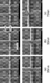
- Fig. 2 conceptually illustrates a state of cell formation at the time of open circuit voltage measurement. It is the image which observed the mode of the cell formation at the time of an open circuit voltage measurement by SEM.
- the crystalline Si layer may be a single crystal Si layer or a polycrystalline Si layer, but in the following description, it is assumed that it is a bulk portion (ie, a single crystal Si layer) of a single crystal silicon substrate. explain.
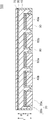
- FIG. 1A is a cross-sectional view for explaining an outline of a first basic structure of a solar cell element according to the present invention.
- a plurality of concave and convex portions 20 are provided over the entire back surface of the p-type conductive silicon substrate 10, and the concave portion 20a has the convex portion 20b as a side wall.
- the p-type silicon substrate 10 is used, but an n-type silicon substrate may be used.
- the depth d from the surface of the silicon substrate 10 to the bottom surface of the recess 20a provided on the back surface of the silicon substrate 10 corresponding to the thickness of the “crystalline Si layer” in the conventional structure is designed to be approximately 100 ⁇ m or less. Therefore, light confinement is effectively performed in the solar cell element, and collection of carriers generated by light incidence is made efficient.
- a desired depth can be set if the depth d to the bottom surface of the recess 20a is approximately 100 ⁇ m or less, but is preferably approximately 10 ⁇ m or more from the viewpoint of ensuring the selected mechanical strength.
- the thickness of the silicon substrate 10 (that is, the sum t of the above d and the height h of the protrusion 20b) is designed to a value (for example, 150 ⁇ m or more) that can sufficiently ensure the mechanical strength.
- a value for example, 150 ⁇ m or more
- the width of the convex portion 20b corresponding to the interval between the concave portions 20a depends on the width of the concave portion 20a, but is preferably in the range of about 50 to 500 ⁇ m from the viewpoint of ensuring mechanical strength.
- a first contact layer (n + silicon layer in this example) 30 having an n-type conductivity is formed on the surface side of the silicon substrate 10, and the first contact layer 30 is formed on each bottom of the recess 20 a.
- a second contact layer (in this example, a p + silicon layer) 40 having a conductivity type opposite to that of the contact layer 30 is formed.
- an amorphous layer having a thickness capable of tunneling carriers may be provided at the interface between the bottom of the recess 20a and the second contact layer 40. Examples of the amorphous layer in this case include an amorphous silicon layer and an amorphous silicon oxide layer.
- the conductivity type of the first contact layer 30 is designed to be opposite to the conductivity type of the silicon substrate 10, but may be designed to be the same as the conductivity type of the silicon substrate 10. . That is, when the p-type silicon substrate 10 is used as shown in FIG. 1A, the conductivity type of the first contact layer 30 may be designed to be p + . In that case, the conductivity type of the second contact layer 40 provided on each bottom of the recess 20a is designed to be n + .
- a first electrode 50 is provided on the first contact layer 30, a second electrode 60 is provided on the second contact layer 40 so as to be electrically connected, and further, on the surface side of the silicon substrate 10.
- an antireflection film (ARC layer) 70 made of SiN x is provided, and the side wall surface of the convex portion 20 b provided on the back surface side of the silicon substrate 10 is covered with a passivation film 80 made of SiO x , for example.
- an insulating material 90 such as SiO x is embedded in the recess 20a to ensure prevention of an electrical short circuit between the second electrodes 60 that are back electrodes. , Improve the mechanical strength.
- the first basic structure of the solar cell element according to the present invention is as follows.
- a plurality of concave and convex portions are provided on the entire back surface of the silicon substrate having the first conductivity type, and the concave portions are separated from each other with the convex portions serving as side walls.
- the depth from the surface of the silicon substrate to the bottom surface of the recess provided on the back surface of the silicon substrate is designed to be 100 ⁇ m or less.
- a first contact layer having a first conductivity type or a second conductivity type opposite to the first conductivity type is formed on the surface side of the silicon substrate.
- a second contact layer having a conductivity type opposite to that of the first contact layer is formed.
- a first electrode connected to the first contact layer and a second electrode connected to the second contact layer are provided.
- the first and second electrodes may be ITO films.
- an antireflection film 70 is provided on the surface side of the silicon substrate 10, and the side wall surface of the convex portion 20b is covered with a passivation film 80. That is, at least the entire exposed surface is covered with the passivation film 80 on the back surface of the silicon substrate 10. Further, an insulating material 90 is embedded in the recess 20a.
- the antireflection film 70 is illustrated as an antireflection structure.
- a texture structure 75 having fine irregularities for confining light may be provided.
- the antireflection structure can be an antireflection film or a texture structure having fine irregularities for light confinement.
- FIG. 2 is a cross-sectional view for explaining the outline of the second basic structure of the solar cell element according to the present invention.
- a surface electric field layer (front surface field layer) 30 is formed in a portion corresponding to the first contact layer described above, and a part of the plurality of recesses 20a.
- a second contact layer 40a having a conductivity type (p + type) opposite to that of the surface electric field layer 30 is formed on the bottom of the surface field layer 30, and the same conductivity type as the surface electric field layer 30 ( n + -type) third contact layers 40b are formed and alternately arranged, and the first electrode 50 shown in FIG. 1A is not essential for the surface electric field layer. The point is different.
- the silicon substrate 10 to be used may be either p-type or n-type, but in FIG. Similar to the basic structure shown in FIG. 1A, a surface electric field layer (n + silicon layer in this example) 30 having n-type conductivity is formed on the surface side of the silicon substrate 10, and a plurality of recesses 20a is formed.
- a second contact layer (a p + silicon layer in this example) 40a having a conductivity type opposite to that of the surface electric field layer 30 is formed at the bottom of some of the layers, and at the bottom of the remaining recesses
- a third contact layer 40 b having the same conductivity type (n + type) as surface electric field layer 30 is formed.
- an oxide film or the like having a thickness that allows carriers to tunnel may be provided at the interface between the bottom of the recess 20a and the second contact layer 40.
- the conductivity type of the surface electric field layer 30 is designed to be opposite to the conductivity type of the silicon substrate 10, but may be designed to be the same as the conductivity type of the silicon substrate 10. That is, in the case of using the silicon substrate 10 of p-type as shown in FIG. 2, may be designed conductivity type of the surface field layer 30 on the p +.
- the second electrode 60a is provided on the second contact layer 40a
- the third electrode 60b is provided on the third contact layer 40b so as to be electrically connected.
- the side wall surface of the projection 20b provided on the back surface side of the silicon substrate 10 is, for example, coated with passivation film 80 of SiO x ing.
- an insulating material 90 such as SiO x is embedded in the recess 20a to prevent electrical short circuit between the second electrode 60a and the third electrode 60b which are back electrodes. At the same time, the mechanical strength is improved.
- the second basic structure of the solar cell element according to the present invention is as follows.
- the back surface of the silicon substrate having the first conductivity type is provided with a plurality of concave and convex portions over the entire surface, and the concave portions are separated from each other with the convex portion as a side wall.
- the depth from the surface of the silicon substrate to the bottom surface of the recess provided on the back surface of the silicon substrate is designed to be 100 ⁇ m or less.
- a surface electric field layer (front surface field layer) having the same conductivity type as the first conductivity type is formed on the surface side of the silicon substrate, and the surface electric field is formed at the bottom of some of the plurality of recesses.
- a second contact layer having a conductivity type opposite to the layer is formed, and a third contact layer having the same conductivity type as the surface electric field layer is formed at the bottom of the remaining recess.
- a second electrode connected to the second contact layer and a third electrode connected to the third contact layer are provided.
- the second and third electrodes may be ITO films.
- an antireflection film 70 is provided on the surface side of the silicon substrate 10, and the side wall surface of the convex portion 20 b is covered with a passivation film 80. Further, an insulating material 90 is embedded in the recess 20a.
- the second electrode 60 may be common to the second contact layers formed in the plurality of recesses 20a.
- the passivation film 80 is also formed in the bottom region of the plurality of recesses 20a, and the second or second structure is formed so as to penetrate the passivation film 80.
- An electrode may be formed on the third contact layer.
- the thickness is such that carriers can pass through the interface region between the contact layer or surface electric field layer and the front or back surface of the silicon substrate by the tunnel effect.
- Amorphous layers 5, 5 a, 5 b may be provided.
- Such an amorphous layer functions as a passivation film for the surface of crystalline silicon, and is effective in suppressing carrier recombination.
- Examples of such an amorphous layer include an amorphous silicon layer and an amorphous silicon oxide layer.
- the amorphous layer is an amorphous silicon layer, the thickness is generally about 2 to 3 nm, for example.
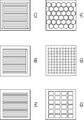
- FIG. 6 is a diagram illustrating the layout of the back electrode of the solar cell element according to the present invention.
- the shape of the second electrode or the third electrode provided at the bottom of the plurality of recesses is a stripe shape ( A to B), a striped comb shape (C), a rectangular shape (D), a circular shape (E), or a honeycomb shape (F), and may have other shapes such as a triangular shape.
- FIG. 7 is a perspective view of a solar cell element provided with a striped back electrode as shown in FIG. 6 (B).
- the passivation film 80 and the insulating material 90 embedded in the recess 20 are not shown.
- FIG. 8 is a diagram illustrating the manufacturing process of the solar cell element according to the present invention by way of example.
- a silicon substrate 10 is prepared (A).
- the silicon substrate 10 has a thickness (for example, 150 ⁇ m or more) that can ensure the strength as a self-supporting substrate.
- the silicon substrate 10 is thermally oxidized to form an oxide film 85 on the front surface, and then a photoresist pattern 15 is provided on the back surface (B).
- the oxide film 85 is patterned by a dry etching process such as a Bosch process or a dry process, and a plurality of recesses 20a are formed on the back surface of the silicon substrate 10 by wet etching such as alkali etching (C).
- a dry etching process such as a Bosch process or a dry process
- a plurality of recesses 20a are formed on the back surface of the silicon substrate 10 by wet etching such as alkali etching (C).
- the passivation film 80 is partially etched by anisotropic dry etching such as ICP. Thereby, the passivation film formed on the bottom of the recess 20a is removed, and the silicon crystal is exposed (D).
- a donor or acceptor dopant is implanted into the silicon crystal region thus exposed by ion implantation or thermal diffusion to form an n + layer or p + layer (E).
- the oxide films (80 and 85) on the surface side are removed by etching (F), and after forming the first contact layer 30 and the antireflection film (ARC layer) 70 (G), the printing method, the sputtering method, etc.
- the front surface electrode 50 and the back surface electrode 60 are formed to complete the device.
- FIG. 9 is a graph showing the results of examining the relationship between the depth d from the surface of the silicon substrate to the bottom surface of the recess provided on the back surface of the silicon substrate and the open circuit voltage. From this graph, it can be seen that the open circuit voltage increases as the depth d decreases.
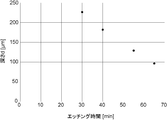
- the depth d can be controlled by changing the etching time. In this embodiment, KOH solution (30 w%) is used as an etchant and etching is performed at a liquid temperature of 80 ° C. In the case of this condition, the relationship between the etching time and the depth d is the relationship shown in FIG.
- a quasi-steady state photoconductivity measurement device (QSS-PC) was used.
- QSS-PC quasi-steady state photoconductivity measurement device
- FIG. 11A Schematic view in top view
- FIG. 11B SEM image of each sample with an etching time of 35 minutes, 50 minutes, and 70 minutes
- the open-circuit voltage of the cell is shown. It is obtained by measuring the time dependency of the electrical conductivity while attenuating the irradiation light and determining the dependency of the lifetime on the injection amount. Therefore, the open circuit voltage obtained is a value that is theoretically estimated from the measurement of minority carrier lifetime. Note that the front and back surfaces of these cells are subjected to passivation with iodine over the entire surface.
- the depth from the surface of the silicon substrate to the bottom surface of the recess provided on the back surface of the silicon substrate is preferably 100 ⁇ m or less.
- the depth is designed to be 100 ⁇ m or less.
- the above-described solar cell element can be used not only as a single element but also as a tandem solar cell including this solar cell element as a bottom cell.
- the back surface of the silicon substrate is provided with a plurality of concave and convex portions over the entire surface, and the concave portions are separated from each other with the convex portions serving as side walls, and at the bottom of the concave portions.
- a contact layer is formed.
Landscapes
- Photovoltaic Devices (AREA)
Abstract
本発明に係る太陽電池素子では、シリコン基板の裏面には全面に渡り複数の凹凸部が設けられており、凹部は凸部を側壁として互いに離間されており、凹部の底部にはコンタクト層が形成されている。このような構造では、機械的強度は凸部で担保されつつ、凹部により高光変換効率化を図ることが可能となる。その結果、シリコン太陽電池セル(素子)としての機械的強度を充分に担保しつつ、高光変換効率化の観点からも有利な構造の超薄型のシリコン太陽電池を提供することが可能となる。
Description
本発明は、太陽電池技術に関し、より詳細には、超薄型のシリコン太陽電池の技術に関する。
近年の環境保全への社会的関心が高まるにつれ、化石燃料に代替するクリーンエネルギーの技術開発の重要性は益々高くなってきている。このような社会背景の下、太陽電池は、自然エネルギーを利用した電力用デバイスとして普及してきたが、太陽電池が主要なエネルギー供給源として利用されるようになるためには、更なるコスト低減と光電変換効率の向上が求められる。
結晶系シリコン太陽電池は、その変換効率の高さから、研究開発が盛んに進められてきており、種々の構造のものが提案されてきている。しかし、結晶系シリコン太陽電池には、モジュール化する際の製造コストに占めるシリコン基板の調達コストの割合が非常に高いという問題がある。このため、シリコン材料費の低減を目的として、シリコン基板の厚さを可能な限り薄くする検討が進められてきた(例えば、特開平8-148709号公報(特許文献1)や特開2013-4554号公報(特許文献2)を参照)。
また、太陽電池におけるシリコン結晶部分が薄くなると、有効に光閉じ込めが行われることとなり、光入射により発生したキャリアの収集が効率的に行われる。また、シリコン結晶部分が薄くなると、フォトキャリアのライフタイムが長くなり、開放電圧を上げることも可能となる。このため、太陽電池のシリコン結晶部分を薄くすることは、製造コスト低減という経済的メリットのみならず、高光変換効率化の観点からも有利である。
しかし、このようなシリコン結晶部分の薄膜化に伴い、機械的強度の低下という問題が生じてくる。厚みの薄いシリコン基板を用いて太陽電池を製造する場合、基板の元厚が100μm以下になると、割れや反りが発生し易くなる。特に、基板の元厚が50μm以下になると、支持基板への貼り付けにより機械的強度を確保することが必須になる。つまり、シリコン結晶部分の薄膜化のために薄いシリコン基板を用いることとすると、基板自体が割れやすくなることはもとより、熱的・機械的なストレスにも弱くなるために反りが生じ易くなる。このようなセルの反りは、モジュール化工程での歩留り低下をもたらしてしまう。
このような機械的強度の低下を抑制するために、いわゆる「貼り合せ技術」を利用して、支持基板側で機械的強度を担保しつつ、シリコン結晶部分の薄膜化を図ろうとする試みもある。
しかし、貼り合せ技術を採用することに伴い、シリコン基板以外に支持基板が必要となること、また、製造プロセス中に貼り合せ工程を組み込む必要が生じることなどから、製造コストを全体としてみると、必ずしもコスト低減にはつながらないという懸念もある。
本発明は、このような問題に鑑みてなされたものであって、その目的とするところは、シリコン太陽電池セル(素子)としての機械的強度を充分に担保しつつ、高光変換効率化の観点からも有利な構造の超薄型のシリコン太陽電池を提供することにある。
上述の課題を解決するために、本発明に係る第1の態様の太陽電池素子は、第1の導電型を有するシリコン基板の裏面には全面に渡り複数の凹凸部が設けられており、前記凹部は前記凸部を側壁として互いに離間されており、前記シリコン基板の表面から前記シリコン基板の裏面に設けられた凹部の底面までの深さが100μm以下であり、前記シリコン基板の表面側には、前記第1の導電型もしくは該第1の導電型と反対の第2の導電型を有する第1のコンタクト層が形成されており、前記複数の凹部の底部には、前記第1のコンタクト層とは反対の導電型を有する第2のコンタクト層が形成されており、前記第1のコンタクト層に接続する第1電極と、前記第2のコンタクト層に接続する第2電極とを備えている、ことを特徴とする。
ある態様では、前記第1のコンタクト層と前記シリコン基板の表面との間に第1の非晶質層が設けられるとともに、前記複数の凹部の底部と前記シリコン基板の裏面との間に第2の非晶質層が設けられており、前記第1および第2の非晶質層は、非晶質シリコン層もしくは非晶質酸化シリコン層である。
また、本発明に係る第2の態様の太陽電池素子は、第1の導電型を有するシリコン基板の裏面には全面に渡り複数の凹凸部が設けられており、前記凹部は前記凸部を側壁として互いに離間されており、前記シリコン基板の表面から前記シリコン基板の裏面に設けられた凹部の底面までの深さが100μm以下であり、前記シリコン基板の表面側には、前記第1の導電型と同じ導電型を有する表面電界層が形成されており、前記複数の凹部のうちの一部の底部には、前記表面電界層とは反対の導電型を有する第2のコンタクト層が形成されるとともに、残りの凹部の底部には前記表面電界層と同じ導電型を有する第3のコンタクト層が形成されており、前記第2のコンタクト層に接続する第2電極と、前記第3のコンタクト層に接続する第3電極とを備えている、ことを特徴とする。
ある態様では、前記表面電界層と前記シリコン基板の表面との間に第1の非晶質層が設けられ、前記複数の凹部のうちの一部の底部と前記シリコン基板の裏面との間に第2の非晶質層が設けられ、前記残りの凹部の底部と前記シリコン基板の裏面との間に第3の非晶質層が設けられており、前記第1、第2、および第3の非晶質層は、非晶質シリコン層もしくは非晶質酸化シリコン層である。
また、ある態様では、前記第2の非晶質層と前記第3の非晶質層は単一の非晶質層である。
これらの態様において、好ましくは、前記シリコン基板の表面側に反射防止構造物が設けられている。このような反射防止構造物は、例えば、反射防止膜もしくは光閉じ込めのための微細な凹凸を有するテクスチャー構造である。
また、好ましくは、前記太陽電池素子の裏面において、少なくとも露出面の全面がパッシベーション膜で被覆されている。
例えば、前記パッシべーション膜はSiO2膜である。
ある態様では、前記凹部に絶縁性物質が埋め込まれている。
また、ある態様では、前記シリコン基板は単結晶シリコン基板である。
例えば、前記反射防止膜は窒化シリコン膜である。
また、例えば、前記第1~3電極の少なくとも何れかは、ITO膜である。
さらに、例えば、前記シリコン基板を裏面側から上面視したときに、前記複数の凹部の底部に設けられた前記第2電極もしくは前記第3電極の形状が、ストライプ状、三角形状、矩形状、円形状、若しくはハニカム状である。
例えば、前記第2電極および前記第3電極の形状がストライプ状であり、櫛歯状電極として形成されている。
上述の太陽電池素子は、これをボトムセルとして備えている太陽電池としての利用も可能である。
本発明に係る太陽電池素子では、シリコン基板の裏面には全面に渡り複数の凹凸部が設けられており、凹部は凸部を側壁として互いに離間されており、凹部の底部にはコンタクト層が形成されている。このような構造では、機械的強度は凸部で担保されつつ、凹部により高光変換効率化を図ることが可能となる。その結果、シリコン太陽電池セル(素子)としての機械的強度を充分に担保しつつ、高光変換効率化の観点からも有利な構造の超薄型のシリコン太陽電池を提供することが可能となる。
以下に、図面を参照して、本発明に係る太陽電池素子の構造について説明する。なお、結晶性Si層は、単結晶Si層であっても多結晶Si層であってもよいが、以降の説明では、単結晶シリコン基板のバルク部分(すなわち単結晶Si層)であるものとして説明する。
[第1の基本構造の概略]
図1Aは、本発明に係る太陽電池素子の第1の基本構造の概略を説明するための断面図である。この図に示した構造例の太陽電池素子100では、p型の導電型のシリコン基板10の裏面に、全面に渡り複数の凹凸部20が設けられており、凹部20aは凸部20bを側壁として、互いに離間されている。なお、この図に示した例では、p型のシリコン基板10を用いているが、n型のシリコン基板を用いることとしてもよい。
図1Aは、本発明に係る太陽電池素子の第1の基本構造の概略を説明するための断面図である。この図に示した構造例の太陽電池素子100では、p型の導電型のシリコン基板10の裏面に、全面に渡り複数の凹凸部20が設けられており、凹部20aは凸部20bを側壁として、互いに離間されている。なお、この図に示した例では、p型のシリコン基板10を用いているが、n型のシリコン基板を用いることとしてもよい。
従来の構造における「結晶性Si層」の厚みに相当することとなる、シリコン基板10の表面からシリコン基板10の裏面に設けられた凹部20aの底面までの深さdは概ね100μm以下に設計され、太陽電池素子における光閉じ込めを有効に行い、光入射により発生したキャリアの収集を効率的なものとしている。なお、この凹部20aの底面までの深さdは概ね100μm以下であれば所望の深さを設定できるが、選択機械的強度の確保等の観点から概ね10μm以上とすることが好ましい。一方、シリコン基板10の厚み(つまり、上記dと凸部20bの高さhの和t)は、機械的強度が十分に担保できる値(例えば150μm以上)に設計される。このような構造では、機械的強度は凸部で担保されつつ、凹部により高光変換効率化を図ることが可能となる。なお、凹部20a相互間の間隔に相当する凸部20bの幅は、凹部20aの幅にも依存するが、機械的強度の確保等の観点から概ね50~500μmの範囲とすることが好ましい。
シリコン基板10の表面側には、n型の導電型を有する第1のコンタクト層(この例ではn+シリコン層)30が形成されており、凹部20aの底部のそれぞれには、上記第1のコンタクト層30とは反対の導電型を有する第2のコンタクト層(この例ではp+シリコン層)40が形成されている。なお、図示はしないが、凹部20aの底部と第2のコンタクト層40との界面に、キャリアがトンネル可能な程度の厚みの非晶質層を設けるようにしてもよい。この場合の非晶質層としては、非晶質シリコン層や非晶質酸化シリコン層を例示することができる。
なお、この図に示した例では、第1のコンタクト層30の導電型を、シリコン基板10の導電型と反対に設計しているが、シリコン基板10の導電型と同じに設計してもよい。つまり、図1Aに示したようにp型のシリコン基板10を用いた場合には、第1のコンタクト層30の導電型をp+に設計してもよい。その場合、凹部20aの底部のそれぞれに設けられる第2のコンタクト層40の導電型は、n+に設計することとなる。
そして、第1のコンタクト層30には第1電極50が、第2のコンタクト層40には第2電極60が、電気的に接続するように設けられ、さらに、シリコン基板10の表面側には、例えばSiNxの反射防止膜(ARC層)70が設けられ、シリコン基板10の裏面側に設けられた凸部20bの側壁面は、例えばSiOxのパッシべーション膜80で被覆されている。なお、この図に示した例では、凹部20aには、例えばSiOxなどの絶縁性物質90が埋め込まれ、裏面電極である第2電極60相互間の電気的短絡防止を確実なものとすると同時に、機械的強度を向上させている。
つまり、本発明に係る太陽電池素子の第1の基本構造とは、下記のものである。第1の導電型を有するシリコン基板の裏面に全面に渡り複数の凹凸部が設けられており、凹部は凸部を側壁として互いに離間されている。そして、シリコン基板の表面からシリコン基板の裏面に設けられた凹部の底面までの深さが100μm以下に設計されている。シリコン基板の表面側には、第1の導電型もしくは該第1の導電型と反対の第2の導電型を有する第1のコンタクト層が形成されており、複数の凹部の底部には、第1のコンタクト層とは反対の導電型を有する第2のコンタクト層が形成されている。そして、第1のコンタクト層に接続する第1電極と、第2のコンタクト層に接続する第2電極とが設けられている。なお、第1および第2電極は、ITO膜であってもよい。
そして、上記基本構造に加え、図1Aに示した態様では、シリコン基板10の表面側に反射防止膜70が設けられ、凸部20bの側壁面はパッシべーション膜80で被覆されている。つまり、シリコン基板10の裏面において、少なくとも露出面の全面がパッシベーション膜80で被覆されている。さらに、凹部20aには、絶縁性物質90が埋め込まれている。
このような構造では、機械的強度は凸部で担保されつつ、凹部により高光変換効率化を図ることが可能となる。つまり、太陽電池素子の製造に際し、支持基板を必要とすることなく、シリコン太陽電池セル(素子)としての機械的強度を充分に担保しつつ、高光変換効率化の観点からも有利な構造の超薄型のシリコン太陽電池を提供することが可能となる。なお、図1Aには反射防止のための構造物として反射防止膜70を例示したが、図1Bに示したような、光閉じ込めのための微細な凹凸を有するテクスチャー構造75を設けるようにしてもよい。つまり、本発明において、反射防止構造物は、反射防止膜や光閉じ込めのための微細な凹凸を有するテクスチャー構造などとすることができる。
[第2の基本構造の概略]
図2は、本発明に係る太陽電池素子の第2の基本構造の概略を説明するための断面図である。図1Aに示した第1の基本構造とは、上述の第1のコンタクト層に相当する部分に表面電界層(フロントサーフェスフィールド層)30が形成されており、複数の凹部20aのうちの一部の底部には、表面電界層30とは反対の導電型(p+型)を有する第2のコンタクト層40aが形成されるとともに、残りの凹部の底部には表面電界層30と同じ導電型(n+型)を有する第3のコンタクト層40bが形成され、これらが交互に配置されている点、また、表面電界層には図1Aに示した第1電極50は必須のものとされていない点、において相違している。
図2は、本発明に係る太陽電池素子の第2の基本構造の概略を説明するための断面図である。図1Aに示した第1の基本構造とは、上述の第1のコンタクト層に相当する部分に表面電界層(フロントサーフェスフィールド層)30が形成されており、複数の凹部20aのうちの一部の底部には、表面電界層30とは反対の導電型(p+型)を有する第2のコンタクト層40aが形成されるとともに、残りの凹部の底部には表面電界層30と同じ導電型(n+型)を有する第3のコンタクト層40bが形成され、これらが交互に配置されている点、また、表面電界層には図1Aに示した第1電極50は必須のものとされていない点、において相違している。
この基本構造においても、用いるシリコン基板10はp型でもn型でもよいが、図2においても、p型のシリコン基板10であるとして図示している。図1Aに示した基本構造と同様に、シリコン基板10の表面側には、n型の導電型を有する表面電界層(この例ではn+シリコン層)30が形成されており、複数の凹部20aのうちの一部のものの底部には、上記表面電界層30とは反対の導電型を有する第2のコンタクト層(この例ではp+シリコン層)40aが形成され、残りの凹部の底部には表面電界層30と同じ導電型(n+型)を有する第3のコンタクト層40bが形成されている。なお、この基本構造においても、図示はしないが、凹部20aの底部と第2のコンタクト層40との界面に、キャリアがトンネル可能な程度の厚みの酸化膜等を設けるようにしてもよい。
この図に示した例においても、表面電界層30の導電型を、シリコン基板10の導電型と反対に設計しているが、シリコン基板10の導電型と同じに設計してもよい。つまり、図2に示したようにp型のシリコン基板10を用いた場合には、表面電界層30の導電型をp+に設計してもよい。
この基本構造では、第2のコンタクト層40aには第2電極60aが、第3のコンタクト層40bには第3電極60bが、電気的に接続するように設けられ、さらに、シリコン基板10の表面側には、例えばSiNxの反射防止膜(ARC層)70が設けられ、シリコン基板10の裏面側に設けられた凸部20bの側壁面は、例えばSiOxのパッシべーション膜80で被覆されている。なお、この図に示した例においても、凹部20aには、例えばSiOxなどの絶縁性物質90が埋め込まれ、裏面電極である第2電極60aと第3電極60b相互間の電気的短絡防止を確実なものとすると同時に、機械的強度を向上させている。
つまり、本発明に係る太陽電池素子の第2の基本構造とは、下記のものである。第1の導電型を有するシリコン基板の裏面には全面に渡り複数の凹凸部が設けられており、凹部は凸部を側壁として互いに離間されている。そして、シリコン基板の表面からシリコン基板の裏面に設けられた凹部の底面までの深さが100μm以下に設計されている。シリコン基板の表面側には、第1の導電型と同じ導電型を有する表面電界層(フロントサーフェスフィールド層)が形成されており、複数の凹部のうちの一部の底部には、前記表面電界層とは反対の導電型を有する第2のコンタクト層が形成されるとともに、残りの凹部の底部には前記表面電界層と同じ導電型を有する第3のコンタクト層が形成されている。そして、第2のコンタクト層に接続する第2電極と、第3のコンタクト層に接続する第3電極とが設けられている。なお、第2および第3電極は、ITO膜であってもよい。
そして、上記基本構造に加え、図2に示した態様では、シリコン基板10の表面側に反射防止膜70が設けられ、凸部20bの側壁面はパッシべーション膜80で被覆されている。さらに、凹部20aには、絶縁性物質90が埋め込まれている。
[その他の構造例]
上記第1および第2の基本構造において、凹部に形成される第2ないし第3のコンタクト層領域は、種々のレイアウト変更が可能である。
上記第1および第2の基本構造において、凹部に形成される第2ないし第3のコンタクト層領域は、種々のレイアウト変更が可能である。
例えば、第1の基本構造においては、図3に示したように、第2電極60を、複数の凹部20aに形成された第2のコンタクト層に共通するものとしてもよい。
また、第1および第2の基本構造において、図4に示したように、複数の凹部20aの底部領域にもパッシベーション膜80を形成し、当該パッシベーション膜80を貫通するような態様で第2ないし第3のコンタクト層に電極形成するようにしてもよい。
さらに、第1および第2の基本構造において、図5に示したように、コンタクト層もしくは表面電界層とシリコン基板の表面もしくは裏面との界面領域に、キャリアがトンネル効果で通過可能な程度の厚みの非晶質層5、5a、5bを設けるようにしてもよい。
このような非晶質層は、結晶質シリコンの表面に対するパッシベーション膜として機能し、キャリアの再結合の抑制に効果がある。斯かる非晶質層としては非晶質シリコン層や非晶質酸化シリコン層を例示することができる。非晶質層が非晶質シリコン層である場合、その厚みは例えば2~3nm程度が一般的である。
この場合も、第2の非晶質層5aと第3の非晶質層5bを単一の非晶質層としても支障はない。
[裏面電極のレイアウト]
図6は、本発明に係る太陽電池素子の裏面電極のレイアウトを例示する図である。レイアウトには種々のものがあり得るが、例えば、シリコン基板を裏面側から上面視したときに、上述の複数の凹部の底部に設けられた第2電極もしくは第3電極の形状として、ストライプ状(A~B)、ストライプ櫛歯状(C)、矩形状(D)、円形状(E)、若しくはハニカム状(F)とすることができ、三角形状等の他の形状としてもよい。
図6は、本発明に係る太陽電池素子の裏面電極のレイアウトを例示する図である。レイアウトには種々のものがあり得るが、例えば、シリコン基板を裏面側から上面視したときに、上述の複数の凹部の底部に設けられた第2電極もしくは第3電極の形状として、ストライプ状(A~B)、ストライプ櫛歯状(C)、矩形状(D)、円形状(E)、若しくはハニカム状(F)とすることができ、三角形状等の他の形状としてもよい。
図7は、図6(B)に図示したようなストライプ状の裏面電極が設けられた太陽電池素子の斜視図である。なお、便宜上、この図では、パッシベーション膜80および凹部20に埋め込まれる絶縁性物質90は不図示とした。
[太陽電池素子の製造プロセス例]
図8は、本発明に係る太陽電池素子の製造プロセスを例示により説明する図である。
図8は、本発明に係る太陽電池素子の製造プロセスを例示により説明する図である。
先ず、シリコン基板10を用意する(A)。このシリコン基板10は、自立基板としての強度を担保できる程度の厚み(例えば150μm以上)のものである。このシリコン基板10を熱酸化して、表面に酸化膜85を形成し、その後、裏面にフォトレジストパターン15を設ける(B)。
次に、ボッシュプロセスなどのドライエッチングプロセスやドライプロセスで酸化膜85をパターニングし、更に、アルカリエッチングなどのウエットエッチングなどによりシリコン基板10の裏面に、凹部20aを複数形成する(C)。
続いて、熱酸化や酸化膜デポジション等により、凹部20aの側壁および底部にパッシベーション膜80を形成した後、ICP等の異方性ドライエッチングによりパッシベーション膜80を部分的にエッチングする。これにより、凹部20aの底部に形成されたパッシベーション膜は除去され、シリコン結晶が露出する(D)。
このようにして露出させたシリコン結晶領域に、イオン注入法や熱拡散法により、ドナーやアクセプターのドーパントを注入して、n+層もしくはp+層とする(E)。
さらに、表面側の酸化膜(80および85)をエッチングにより除去し(F)、第1のコンタクト層30および反射防止膜(ARC層)70を形成したのち(G)、印刷法やスパッタリング法などにより、表面電極50および裏面電極60を形成して、素子が完成する。
図9は、シリコン基板の表面からシリコン基板の裏面に設けられた凹部の底面までの深さdと開放電圧との関係を調べた結果を示すグラフである。このグラフから、開放電圧は上記深さdが小さくなるほど高い値を示すことが読み取れる。なお、上記深さdは、エッチング時間を変えることで制御できる。この実施例では、KOH溶液(30w%)をエッチャントとし、液温80℃でエッチングを行っている。この条件の場合、エッチング時間と上記深さdの関係は、図10に示した関係を示す。
この開放電圧の測定に際しては、擬定常状態光伝導度測定装置(QSS-PC)を用いた。この測定装置では、図11A(上面視概略図)および図11B(エッチング時間が35分、50分、70分の各試料のSEM像)に示したようにセル化した時のセルの開放電圧を、照射光を減衰させながら電気伝導度の時間依存性を測り、ライフタイムの注入量依存性を求めることで得ている。よって、得られる開放電圧は、少数キャリアライフタイムの測定から理論的に推定される値である。なお、これらのセルの表面および裏面は、全面に渡り、ヨウ素によるパッシベーションが施されている。
このように、開放電圧の観点から、シリコン基板の表面からシリコン基板の裏面に設けられた凹部の底面までの深さは100μm以下であることが好ましい。本発明ではこの結果に基づき、上記深さを100μm以下に設計している。
なお、上述の太陽電池素子は、単独の素子としての使用はもとより、この太陽電池素子をボトムセルとして備えたタンデム型の太陽電池としての利用も可能である。
このように、本発明に係る太陽電池素子では、シリコン基板の裏面には全面に渡り複数の凹凸部が設けられており、凹部は凸部を側壁として互いに離間されており、凹部の底部にはコンタクト層が形成されている。このような構造では、機械的強度は凸部で担保されつつ、凹部により高光変換効率化を図ることが可能となる。その結果、シリコン太陽電池セル(素子)としての機械的強度を充分に担保しつつ、高光変換効率化の観点からも有利な構造の超薄型のシリコン太陽電池を提供することが可能となる。
5、5a、5b 非晶質層
10 シリコン基板10
15 フォトレジスト
20 凹凸部
20a 凹部
20b 凸部
30 第1のコンタクト層
40 第2のコンタクト層
50 第1電極
60 第2電極
70 反射防止膜(ARC層)
75 テクスチャー構造
80 パッシべーション膜
85 酸化膜
90 絶縁性物質
100 太陽電池素子
10 シリコン基板10
15 フォトレジスト
20 凹凸部
20a 凹部
20b 凸部
30 第1のコンタクト層
40 第2のコンタクト層
50 第1電極
60 第2電極
70 反射防止膜(ARC層)
75 テクスチャー構造
80 パッシべーション膜
85 酸化膜
90 絶縁性物質
100 太陽電池素子
Claims (15)
- 第1の導電型を有するシリコン基板の裏面には全面に渡り複数の凹凸部が設けられており、
前記凹部は前記凸部を側壁として互いに離間されており、
前記シリコン基板の表面から前記シリコン基板の裏面に設けられた凹部の底面までの深さが100μm以下であり、
前記シリコン基板の表面側には、前記第1の導電型もしくは該第1の導電型と反対の第2の導電型を有する第1のコンタクト層が形成されており、
前記複数の凹部の底部には、前記第1のコンタクト層とは反対の導電型を有する第2のコンタクト層が形成されており、
前記第1のコンタクト層に接続する第1電極と、前記第2のコンタクト層に接続する第2電極とを備えている太陽電池素子。 - 前記第1のコンタクト層と前記シリコン基板の表面との間に第1の非晶質層が設けられるとともに、前記複数の凹部の底部と前記シリコン基板の裏面との間に第2の非晶質層が設けられており、
前記第1および第2の非晶質層は、非晶質シリコン層もしくは非晶質酸化シリコン層である、請求項1に記載の太陽電池素子。 - 第1の導電型を有するシリコン基板の裏面には全面に渡り複数の凹凸部が設けられており、
前記凹部は前記凸部を側壁として互いに離間されており、
前記シリコン基板の表面から前記シリコン基板の裏面に設けられた凹部の底面までの深さが100μm以下であり、
前記シリコン基板の表面側には、前記第1の導電型と同じ導電型を有する表面電界層が形成されており、
前記複数の凹部のうちの一部の底部には、前記表面電界層とは反対の導電型を有する第2のコンタクト層が形成されるとともに、残りの凹部の底部には前記表面電界層と同じ導電型を有する第3のコンタクト層が形成されており、
前記第2のコンタクト層に接続する第2電極と、前記第3のコンタクト層に接続する第3電極とを備えている太陽電池素子。 - 前記表面電界層と前記シリコン基板の表面との間に第1の非晶質層が設けられ、前記複数の凹部のうちの一部の底部と前記シリコン基板の裏面との間に第2の非晶質層が設けられ、前記残りの凹部の底部と前記シリコン基板の裏面との間に第3の非晶質層が設けられており、
前記第1、第2、および第3の非晶質層は、非晶質シリコン層もしくは非晶質酸化シリコン層である、請求項3に記載の太陽電池素子。 - 前記第2の非晶質層と前記第3の非晶質層は単一の非晶質層である、請求項4に記載の太陽電池素子。
- 前記シリコン基板の表面側に反射防止構造物が設けられている、請求項1~5の何れか1項に記載の太陽電池素子。
- 前記反射防止構造物は、反射防止膜もしくは光閉じ込めのための微細な凹凸を有するテクスチャー構造である、請求項6に記載の太陽電池素子。
- 前記太陽電池素子の裏面において、少なくとも露出面の全面がパッシベーション膜で被覆されている、請求項1~5の何れか1項に記載の太陽電池素子。
- 前記パッシベーション膜はSiO2膜である、請求項8に記載の太陽電池素子。
- 前記凹部に絶縁性物質が埋め込まれている、請求項1~5の何れか1項に記載の太陽電池素子。
- 前記シリコン基板は単結晶シリコン基板である、請求項1~5の何れか1項に記載の太陽電池素子。
- 前記反射防止膜は窒化シリコン膜である、請求項1~5の何れか1項に記載の太陽電池素子。
- 前記第1~3電極の少なくとも何れかは、ITO膜である、請求項1~5の何れか1項に記載の太陽電池素子。
- 前記シリコン基板を裏面側から上面視したときに、前記複数の凹部の底部に設けられた前記第2電極もしくは前記第3電極の形状が、ストライプ状、三角形状、矩形状、円形状、若しくはハニカム状である、請求項1~5の何れか1項に記載の太陽電池素子。
- 前記第2電極および前記第3電極の形状がストライプ状であり、櫛歯状電極として形成されている、請求項14に記載の太陽電池素子。
Applications Claiming Priority (2)
| Application Number | Priority Date | Filing Date | Title |
|---|---|---|---|
| JP2016142379A JP2019165033A (ja) | 2016-07-20 | 2016-07-20 | 太陽電池素子 |
| JP2016-142379 | 2016-07-20 |
Publications (1)
| Publication Number | Publication Date |
|---|---|
| WO2018016548A1 true WO2018016548A1 (ja) | 2018-01-25 |
Family
ID=60992603
Family Applications (1)
| Application Number | Title | Priority Date | Filing Date |
|---|---|---|---|
| PCT/JP2017/026172 Ceased WO2018016548A1 (ja) | 2016-07-20 | 2017-07-20 | 太陽電池素子 |
Country Status (2)
| Country | Link |
|---|---|
| JP (1) | JP2019165033A (ja) |
| WO (1) | WO2018016548A1 (ja) |
Cited By (4)
| Publication number | Priority date | Publication date | Assignee | Title |
|---|---|---|---|---|
| CN113299770A (zh) * | 2021-06-04 | 2021-08-24 | 浙江爱旭太阳能科技有限公司 | 一种选择性接触区域掩埋型太阳能电池及其背面接触结构 |
| WO2022073628A1 (en) * | 2021-06-04 | 2022-04-14 | Solarlab Aiko Europe Gmbh | Back contact structure and selective contact region buried solar cell comprising the same |
| CN120568864A (zh) * | 2025-07-31 | 2025-08-29 | 横店集团东磁股份有限公司 | 背接触太阳能电池及其制备方法、电池组件 |
| WO2026031715A1 (zh) * | 2024-08-09 | 2026-02-12 | 山东爱旭太阳能科技有限公司 | 背接触太阳能电池、电池组件和光伏系统 |
Citations (3)
| Publication number | Priority date | Publication date | Assignee | Title |
|---|---|---|---|---|
| JP2010251343A (ja) * | 2009-04-10 | 2010-11-04 | Mitsubishi Electric Corp | 太陽電池およびその製造方法 |
| US20110056548A1 (en) * | 2009-09-09 | 2011-03-10 | Li-Karn Wang | Wafer-Based Solar Cell with Deeply Etched Structure |
| JP2015191962A (ja) * | 2014-03-27 | 2015-11-02 | 三菱電機株式会社 | 太陽電池およびその製造方法 |
-
2016
- 2016-07-20 JP JP2016142379A patent/JP2019165033A/ja active Pending
-
2017
- 2017-07-20 WO PCT/JP2017/026172 patent/WO2018016548A1/ja not_active Ceased
Patent Citations (3)
| Publication number | Priority date | Publication date | Assignee | Title |
|---|---|---|---|---|
| JP2010251343A (ja) * | 2009-04-10 | 2010-11-04 | Mitsubishi Electric Corp | 太陽電池およびその製造方法 |
| US20110056548A1 (en) * | 2009-09-09 | 2011-03-10 | Li-Karn Wang | Wafer-Based Solar Cell with Deeply Etched Structure |
| JP2015191962A (ja) * | 2014-03-27 | 2015-11-02 | 三菱電機株式会社 | 太陽電池およびその製造方法 |
Cited By (9)
| Publication number | Priority date | Publication date | Assignee | Title |
|---|---|---|---|---|
| CN113299770A (zh) * | 2021-06-04 | 2021-08-24 | 浙江爱旭太阳能科技有限公司 | 一种选择性接触区域掩埋型太阳能电池及其背面接触结构 |
| WO2022073626A1 (en) * | 2021-06-04 | 2022-04-14 | Solarlab Aiko Europe Gmbh | Back contact structure and selective contact region buried solar cell comprising the same |
| WO2022073628A1 (en) * | 2021-06-04 | 2022-04-14 | Solarlab Aiko Europe Gmbh | Back contact structure and selective contact region buried solar cell comprising the same |
| US11450777B1 (en) | 2021-06-04 | 2022-09-20 | Solarlab Aiko Europe Gmbh | Back contact structure and selective contact region buried solar cell comprising the same |
| EP4099408A1 (en) * | 2021-06-04 | 2022-12-07 | Solarlab Aiko Europe GmbH | Back contact structure and selective contact region buried solar cell comprising the same |
| EP4099407A1 (en) * | 2021-06-04 | 2022-12-07 | Solarlab Aiko Europe GmbH | Back contact structure and selective contact region buried solar cell comprising the same |
| US11695087B2 (en) | 2021-06-04 | 2023-07-04 | Solarlab Aiko Europe Gmbh | Back contact structure and selective contact region buried solar cell comprising the same |
| WO2026031715A1 (zh) * | 2024-08-09 | 2026-02-12 | 山东爱旭太阳能科技有限公司 | 背接触太阳能电池、电池组件和光伏系统 |
| CN120568864A (zh) * | 2025-07-31 | 2025-08-29 | 横店集团东磁股份有限公司 | 背接触太阳能电池及其制备方法、电池组件 |
Also Published As
| Publication number | Publication date |
|---|---|
| JP2019165033A (ja) | 2019-09-26 |
Similar Documents
| Publication | Publication Date | Title |
|---|---|---|
| CN104282782B (zh) | 太阳能电池及其制造方法 | |
| CN106159008B (zh) | 太阳能电池及其制造方法 | |
| CN104167454B (zh) | 太阳能电池及其制造方法 | |
| CN201681950U (zh) | 用于高功率重量比应用的背接触式太阳能电池 | |
| TWI455342B (zh) | Solar cell with selective emitter structure and manufacturing method thereof | |
| JP2011512687A (ja) | 非対称ウエーハのエッチング方法、非対称エッチングのウエーハを含む太陽電池、及び太陽電池の製造方法 | |
| JP7779465B2 (ja) | バックコンタクトヘテロ接合電池セルおよびその製造方法 | |
| US20100288346A1 (en) | Configurations and methods to manufacture solar cell device with larger capture cross section and higher optical utilization efficiency | |
| CN115566099A (zh) | 一种太阳能电池的制造方法 | |
| US8334160B2 (en) | Semiconductor photovoltaic devices and methods of manufacturing the same | |
| WO2018016548A1 (ja) | 太陽電池素子 | |
| TWI538244B (zh) | Method for manufacturing solar cells | |
| CN119997663B (zh) | 一种背接触电池及其制备方法、光伏系统 | |
| CN103890961B (zh) | 具有浮动正面发射极区的交指型背面接点光伏电池 | |
| JP2013120863A (ja) | 太陽電池の製造方法 | |
| CN120568917B (zh) | 一种背接触太阳能电池及其制备方法 | |
| CN121038370A (zh) | 太阳能电池及其制备方法 | |
| KR20200107907A (ko) | 태양 전지 및 이의 제조 방법 | |
| KR101680384B1 (ko) | 태양 전지의 제조 방법 | |
| KR100997112B1 (ko) | 태양 전지 | |
| JP5554359B2 (ja) | 基板の粗面化方法、太陽電池の製造方法および太陽電池、太陽電池モジュール | |
| KR101237556B1 (ko) | 양면 수광형 국부화 에미터 태양전지 | |
| JP2013168605A (ja) | 太陽電池の製造方法 | |
| KR102132741B1 (ko) | 태양 전지 및 이의 제조 방법 | |
| TWI462308B (zh) | 半導體光電元件及其製造方法 |
Legal Events
| Date | Code | Title | Description |
|---|---|---|---|
| 121 | Ep: the epo has been informed by wipo that ep was designated in this application |
Ref document number: 17831064 Country of ref document: EP Kind code of ref document: A1 |
|
| NENP | Non-entry into the national phase |
Ref country code: DE |
|
| 122 | Ep: pct application non-entry in european phase |
Ref document number: 17831064 Country of ref document: EP Kind code of ref document: A1 |
|
| NENP | Non-entry into the national phase |
Ref country code: JP |