WO2018016404A1 - ホウ素ドープダイヤモンド - Google Patents
ホウ素ドープダイヤモンド Download PDFInfo
- Publication number
- WO2018016404A1 WO2018016404A1 PCT/JP2017/025473 JP2017025473W WO2018016404A1 WO 2018016404 A1 WO2018016404 A1 WO 2018016404A1 JP 2017025473 W JP2017025473 W JP 2017025473W WO 2018016404 A1 WO2018016404 A1 WO 2018016404A1
- Authority
- WO
- WIPO (PCT)
- Prior art keywords
- boron
- diamond
- doped
- doped diamond
- range
- Prior art date
- Legal status (The legal status is an assumption and is not a legal conclusion. Google has not performed a legal analysis and makes no representation as to the accuracy of the status listed.)
- Ceased
Links
Images
Classifications
-
- C—CHEMISTRY; METALLURGY
- C01—INORGANIC CHEMISTRY
- C01B—NON-METALLIC ELEMENTS; COMPOUNDS THEREOF; METALLOIDS OR COMPOUNDS THEREOF NOT COVERED BY SUBCLASS C01C
- C01B32/00—Carbon; Compounds thereof
- C01B32/25—Diamond
-
- C—CHEMISTRY; METALLURGY
- C23—COATING METALLIC MATERIAL; COATING MATERIAL WITH METALLIC MATERIAL; CHEMICAL SURFACE TREATMENT; DIFFUSION TREATMENT OF METALLIC MATERIAL; COATING BY VACUUM EVAPORATION, BY SPUTTERING, BY ION IMPLANTATION OR BY CHEMICAL VAPOUR DEPOSITION, IN GENERAL; INHIBITING CORROSION OF METALLIC MATERIAL OR INCRUSTATION IN GENERAL
- C23C—COATING METALLIC MATERIAL; COATING MATERIAL WITH METALLIC MATERIAL; SURFACE TREATMENT OF METALLIC MATERIAL BY DIFFUSION INTO THE SURFACE, BY CHEMICAL CONVERSION OR SUBSTITUTION; COATING BY VACUUM EVAPORATION, BY SPUTTERING, BY ION IMPLANTATION OR BY CHEMICAL VAPOUR DEPOSITION, IN GENERAL
- C23C16/00—Chemical coating by decomposition of gaseous compounds, without leaving reaction products of surface material in the coating, i.e. chemical vapour deposition [CVD] processes
- C23C16/22—Chemical coating by decomposition of gaseous compounds, without leaving reaction products of surface material in the coating, i.e. chemical vapour deposition [CVD] processes characterised by the deposition of inorganic material, other than metallic material
- C23C16/26—Deposition of carbon only
- C23C16/27—Diamond only
-
- C—CHEMISTRY; METALLURGY
- C30—CRYSTAL GROWTH
- C30B—SINGLE-CRYSTAL GROWTH; UNIDIRECTIONAL SOLIDIFICATION OF EUTECTIC MATERIAL OR UNIDIRECTIONAL DEMIXING OF EUTECTOID MATERIAL; REFINING BY ZONE-MELTING OF MATERIAL; PRODUCTION OF A HOMOGENEOUS POLYCRYSTALLINE MATERIAL WITH DEFINED STRUCTURE; SINGLE CRYSTALS OR HOMOGENEOUS POLYCRYSTALLINE MATERIAL WITH DEFINED STRUCTURE; AFTER-TREATMENT OF SINGLE CRYSTALS OR A HOMOGENEOUS POLYCRYSTALLINE MATERIAL WITH DEFINED STRUCTURE; APPARATUS THEREFOR
- C30B29/00—Single crystals or homogeneous polycrystalline material with defined structure characterised by the material or by their shape
- C30B29/02—Elements
- C30B29/04—Diamond
Definitions
- the present invention relates to boron-doped diamond in which boron is doped into diamond.
- Diamond has excellent properties such as a high breakdown electric field (> 10 MV / cm), high-speed carrier mobility (electrons: 4500 cm 2 / Vs, holes: 3800 cm 2 / Vs), and the highest thermal conductivity (22 W / cmK) in the substance. Therefore, it is expected to be applied as a power device material that operates in a high temperature / extreme environment because of its excellent chemical stability and radiation resistance.
- Patent Document 1 describes a semiconductor diamond containing carbon as a main component and containing nitrogen atoms and boron atoms, both of which have a concentration of 1000 ppm or more.
- a single crystal structure doped with boron by forming a source gas containing a nitrogen source, a boron source, and a carbon source using a microwave CVD method is used. It is said that a boron-doped diamond film is obtained.
- a boron-doped single crystal diamond doped with boron can be obtained by using a method as described in Patent Document 1.
- boron concentration for example, the boron concentration is more than 1 ⁇ 10 19 cm ⁇ 3
- boron is incorporated at sites other than the substitution atom position, and the electric resistance value is increased. There is a problem that becomes larger.
- the main object of the present invention is to provide a boron-doped diamond having a small electric resistance value despite containing boron at a high concentration.
- the present inventors have intensively studied to solve the above problems.
- boron concentration was measured by secondary ion mass spectrometry, there 1 ⁇ 10 19 cm -3 greater, in the range of 1 ⁇ 10 22 cm -3 or less , Measured by X-ray absorption fine structure analysis (NEXAFS), the peak intensity A of the X-ray photon energy located in the range of 288 eV to 290 eV, and the X-ray photon energy range of 286.2 eV to 288.5 eV.
- the boron-doped diamond having a ratio (B / A) with the peak intensity area B in FIG. 3 of 0.30 or less was found to have a very low electrical resistance value despite containing a high concentration of boron. .
- boron concentration measured by secondary ion mass spectrometry in boron-doped diamond is in the range of more than 1 ⁇ 10 19 cm ⁇ 3 and 1 ⁇ 10 22 cm ⁇ 3 or less, and X-ray Positions of 187.1 eV and 189.1 eV indicating the presence of clusters in which boron atoms are bonded to each other in the X-ray absorption spectrum of boron atoms from the 1s orbital to the outer shell, as measured by absorption fine structure analysis (NEXAFS) It was also found that the boron-doped diamond having substantially no peak has a very low electric resistance value even though it contains a high concentration of boron.
- this invention provides the invention of the aspect hung up below.
- Item 1 Boron-doped diamond in which diamond is doped with boron, The boron concentration measured by secondary ion mass spectrometry is in the range of more than 1 ⁇ 10 19 cm ⁇ 3 and 1 ⁇ 10 22 cm ⁇ 3 or less, The peak intensity A of the diamond core exonton located in the range of X-ray photon energy 288 eV to 290 eV and the range of X-ray photon energy 286.2 eV to 288.5 eV, as measured by X-ray absorption fine structure analysis (NEXAFS) A boron-doped diamond having a ratio (B / A) with a peak intensity area B of 0.30 or less.
- Boron-doped diamond in which diamond is doped with boron The boron concentration measured by secondary ion mass spectrometry is in the range of more than 1 ⁇ 10 19 cm ⁇ 3 and 1 ⁇ 10 22 cm ⁇ 3 or less, 187.1 eV and 189.1 eV which show that the cluster which the boron atom couple
- Item 5. The boron-doped diamond according to any one of Items 1 to 4, wherein a difference between a maximum value and a minimum value of the thickness of the boron-doped diamond is 10% or less of the maximum value.
- Item 6. Item 6. The boron-doped diamond according to any one of Items 1 to 5, which is formed on a substrate.
- Item 7. An electronic device comprising the boron-doped diamond according to any one of Items 1 to 6.
- the boron-doped diamond of the present invention is a boron-doped diamond in which diamond is doped with boron.
- the crystal structure of boron-doped diamond may be single crystal or polycrystalline.
- boron-doped single crystal diamond can be obtained.
- a polycrystalline diamond substrate is used, boron-doped polycrystalline diamond can be obtained.
- a heterogeneous substrate Si, SiC, GaN, WC, etc.
- the boron concentration measured by secondary ion mass spectrometry is in the range of more than 1 ⁇ 10 19 cm ⁇ 3 and 1 ⁇ 10 22 cm ⁇ 3 or less.
- the peak intensity A of the diamond core exonton located in the range of X-ray photon energy 288 eV to 290 eV measured by X-ray absorption fine structure analysis (NEXAFS) The ratio (B / A) to the peak intensity area B in the range of X-ray photon energy of 286.2 eV to 288.5 eV is 0.30 or less.
- the specific measuring method by NEXAFS is as having described in the Example.
- the first boron-doped diamond of the present invention since the peak intensity area ratio (B / A) is 0.30 or less, the boron concentration is more than 1 ⁇ 10 19 cm ⁇ 3 , 1 Despite the high concentration in the range of ⁇ 10 22 cm ⁇ 3 or less, the peak intensity area ratio (B / A) is 0.30 or less, and a cluster in which boron atoms contained in boron-doped diamond are bonded to each other Is virtually absent. For this reason, the first boron-doped diamond has a feature that boron is incorporated at a substitution atom position and the electric resistance value is small.
- the boron atoms couple
- the peaks observed at the positions of 187.1 eV and 189.1 eV are caused by clusters in which boron in the boron-doped diamond is bonded to each other.
- boron in the boron-doped diamond is bonded to each other.
- the boron concentration measured by secondary ion mass spectrometry is in the range of more than 1 ⁇ 10 19 cm ⁇ 3 and 1 ⁇ 10 22 cm ⁇ 3 or less, and the X-ray absorption fineness In the X-ray absorption spectrum from the 1s orbital of boron atoms to the outer shell, measured by structural analysis (NEXAFS), peaks at positions of 187.1 eV and 189.1 eV indicating the presence of clusters in which boron atoms are bonded to each other. It is characterized by not having substantially.
- the electrical resistance value of the boron-doped diamond of the present invention is not particularly limited, but from the viewpoint of being suitably used as an electronic device described later, for example, the electrical resistance value at a temperature of 25 ° C. is preferably 30 m ⁇ cm or less, more preferably 25 m ⁇ cm. Hereinafter, more preferably 5 m ⁇ cm or less.
- the lower limit value of the electrical resistance value is usually about 0.1 m ⁇ cm.
- the electrical resistance value is a value measured by the Hall effect, and specific measurement conditions are as described in the examples described later.
- the boron-doped diamond of the present invention has a crystal structure in which some of the carbon atoms of the diamond are replaced by boron atoms.
- the boron-doped diamond may contain impurities other than boron (for example, phosphorus). Impurities other than boron may be included singly or in combination of two or more.
- the boron-doped diamond of the present invention can be suitably produced by a hot filament CVD method.
- a hot filament CVD method As a method for producing the boron-doped diamond of the present invention, for example, it can be suitably produced by a hot filament CVD method.
- a hot filament CVD method As a method for producing the boron-doped diamond of the present invention, for example, it can be suitably produced by a hot filament CVD method.
- a hot filament CVD method As a method for producing the boron-doped diamond of the present invention, for example, it can be suitably produced by a hot filament CVD method.
- a metal element for example, tungsten
- tungsten which constitutes the filament
- boron-doped diamond having a single crystal structure cannot be suitably manufactured.
- boron-doped diamond having a single crystal structure can be synthesized.
- boron-doped diamond having a single crystal structure can be suitably obtained by employing a hot filament CVD method. Furthermore, the present inventors have adopted a hot filament CVD method, so that a high concentration of boron (for example, a boron concentration measured by secondary ion mass spectrometry is 1 ⁇ 10 19 cm ⁇ ) even by synthesis over a long period of time. It has been found that boron-doped diamond doped with more than 3 ) can be synthesized, soot is not deposited in the chamber, and boron-doped diamond having a single crystal structure and excellent crystal quality can be obtained. It was also found that boron-doped diamond can be made thicker and larger in area.
- boron-doped diamond produced by a hot filament CVD method usually contains a metal element (for example, tungsten described later) constituting the hot filament.
- boron-doped diamond synthesized by the microwave CVD method does not contain such a metal element.
- the boron-doped diamond of the present invention may contain a metal element different from boron in addition to the above boron.
- the metal element constituting the filament is usually contained in the boron-doped diamond.
- Specific examples of the metal element include tungsten, tantalum, rhenium, ruthenium and the like.
- the concentration of the metal element is not particularly limited, and examples thereof include a range of about 1 ⁇ 10 16 to 1 ⁇ 10 20 cm ⁇ 3 .
- concentration of the metal element in boron dope diamond is the value measured by secondary ion mass spectrometry (SIMS).
- the thickness of the boron-doped diamond of the present invention is not particularly limited, and for example, about 0.01 ⁇ m to 1 mm, more preferably about 0.1 to 500 ⁇ m can be mentioned.
- the boron concentration that can be a thick film of about 0.1 ⁇ m to 1 mm is 1.2 ⁇ 10 20 cm ⁇ 3 is considered the limit (see, for example, Appl. Phys. Lett. 100 (2012) 122109).
- the thickness of the boron-doped diamond can be set to about 0.1 ⁇ m to 1 mm.
- the difference between the maximum value and the minimum value of the boron-doped diamond of the present invention is preferably 10% or less of the maximum value, and more preferably 5% or less. If boron-doped diamond is synthesized by a hot filament CVD method, such a boron-doped diamond with high thickness uniformity can be obtained.
- the boron-doped diamond of the present invention can be formed on a substrate using, for example, a hot filament CVD method, it may have a form formed on the substrate.
- the substrate include single crystal diamond, polycrystalline diamond, 3C silicon carbide, iridium, and platinum.
- the boron-doped diamond of the present invention contains boron at a high concentration as described above, and further has a small crystal lattice distortion and a small electrical resistance value. Therefore, materials for electronic devices such as diodes and transistors (particularly, Suitable as a power device material). That is, according to the present invention, an electronic device containing boron-doped diamond can be provided. Examples of the electronic device using the boron-doped diamond of the present invention include a Schottky diode, a PN junction diode, a field effect transistor, a deep ultraviolet detector, and an electron emitter.
- Step (1) Step of introducing a carrier gas containing a carbon source and a boron source into a vacuum vessel in which the substrate and the filament are arranged
- Step (2) Heating the carrier gas with a filament to form diamond containing boron Film forming process to form a film on top
- the metal constituting the filament disposed in the vacuum vessel is not particularly limited as long as it can constitute the filament.
- the metal element include tungsten, tantalum, rhenium, ruthenium, etc. Among these, tungsten is preferable.
- a metal element may be used individually by 1 type and may be used in combination of 2 or more types.
- the substrate disposed in the vacuum vessel is boron having a diamond crystal structure in which a carbon source and boron contained in a carrier gas are formed on the substrate in the later-described step (2). If it can grow a dope diamond, it will not restrict
- Specific examples of the substrate include single crystal diamond, polycrystalline diamond, 3C silicon carbide, iridium, and platinum.
- a carrier gas containing a carbon source and a boron source is introduced.
- the carbon source is not particularly limited as long as it can form diamond, and examples thereof include methane.
- a carbon source may be used individually by 1 type and may be used in combination of 2 or more types.
- the boron source is not particularly limited as long as it can be doped into diamond as boron and can maintain the crystal structure of diamond, and preferably includes trimethylboron, diborane and the like.
- a boron source may be used individually by 1 type and may be used in combination of 2 or more types.
- the carrier gas is not particularly limited, and for example, hydrogen gas can be used.
- the concentration of the carbon source in the carrier gas is preferably about 0.5 to 5.0% by volume, more preferably about 1.0 to 3.0% by volume.
- concentration contained in boron dope diamond is preferably 100 ppm. More preferably, about 1000 to 20000 ppm, more preferably about 5000 to 10,000 ppm.
- a carrier gas is heated with a filament to perform a film forming step of forming boron-doped diamond on the substrate.
- the heating temperature of the filament may be appropriately set according to the type of metal element constituting the filament to be used and the concentration of boron contained in the boron-doped diamond, preferably about 2000 to 2400 ° C., more preferably 2000 Up to about 2200 ° C can be mentioned.
- the total pressure in the vacuum vessel in the step (2) is not particularly limited, and for example, about 10 to 100 Torr, more preferably about 10 to 80 Torr.
- the temperature of the substrate in the step (2) is not particularly limited, and may be about 700 to 1100 ° C., more preferably about 700 to 900 ° C., for example.
- the film forming time in step (2) may be appropriately selected according to the target thickness and the like, and is usually about 3 to 50 hours.
- the boron concentration in diamond can be set to be more than 1 ⁇ 10 19 and 1 ⁇ 10 22 cm ⁇ 3 or less.
- the concentration of boron in the boron-doped diamond is 1 ⁇ 10 19 by setting the concentration of the boron source to the carbon source in the carrier gas preferably to 100 ppm or more. cm -3 greater, it can be adjusted to be 1 ⁇ 10 22 cm -3 or less.
- the concentration of the carbon source in the carrier gas is 0.1 to 5.0% by volume
- the total pressure in the vacuum vessel is 10 to 80 Torr
- Boron doping containing boron at a high concentration of more than 1 ⁇ 10 19 cm ⁇ 3 by setting the substrate temperature to 700 to 900 ° C. and setting the off angle in the pretreatment of the substrate to 0.5 to 3 ° Diamond can be particularly preferably produced.
- the boron-doped diamond of the present invention can be suitably produced.
- Example 1-3 Boron-doped single crystal diamond was formed on the surface of the single crystal diamond substrate (100) by a hot filament chemical vapor deposition method (hot filament CVD method).
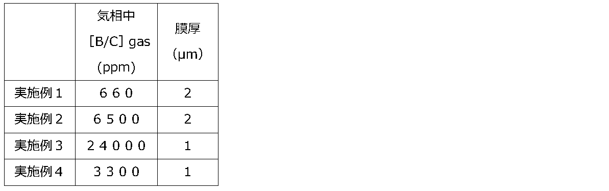
- the film forming conditions in each example are as follows. (Film forming conditions) Carrier gas: 97% by volume of hydrogen, 3% by volume of methane (carbon source), and the volume concentration of trimethylboron (boron source) with respect to methane ([B / C] gas , ppm in the gas phase) is shown in Table 1, respectively. As described.
- Example 4 Boron-doped polycrystalline diamond was formed on the surface of the damaged Si substrate by hot filament chemical vapor deposition (hot filament CVD).
- the film forming conditions are as follows. (Film forming conditions) Carrier gas: 97% by volume of hydrogen, 3% by volume of methane (carbon source), and the volume concentration of trimethylboron (boron source) relative to methane ([B / C] gas , ppm in the gas phase) is shown in Table 1. It is as follows.
- ⁇ Comparative Example 1> A commercially available boron-doped single crystal diamond substrate (manufactured by TISNCM, type-IIb substrate, plane orientation (100), boron concentration: about 10 20 cm ⁇ 3 , substrate thickness: 300 ⁇ m) prepared by a high temperature and high pressure method was used. .
- the film forming conditions are as follows. (Film forming conditions) Carrier gas: 97% by volume of hydrogen, 3% by volume of methane (carbon source), and the volume concentration of trimethylboron (boron source) relative to methane ([B / C] gas , ppm in the gas phase) is 10,000% by volume.
- Film formation time 10 hours ⁇ Boron doped single crystal diamond film thickness: 1 ⁇ m ⁇ Off-angle of substrate pretreatment: 2.5 °
- X-ray absorption fine structure analysis C1s
- the boron-doped diamond obtained in Examples 1, 2, 4 and Comparative Examples 1, 2 was subjected to X-ray absorption fine structure analysis (NEXAFS).
- NEXAFS X-ray absorption fine structure analysis
- an X-ray absorption spectrum from 1 s of carbon of the host element to the outer shell is used. That is, the spectrum is obtained by scanning the X-ray photon energy in the vicinity of the absorption edge of carbon atoms (275 eV to 345 eV) and detecting the energy loss in the absorption process.
- an electron yield method total electron yield: TEY
- a fluorescence yield method fluorescence yield: FY
- the TEY method was used to confirm clusters in which boron atoms contained in boron-doped diamond were bonded to each other.
- NEXAFS the surfaces of the boron-doped diamonds obtained in Example 3-5 and Comparative Examples 1 and 2 were cleaned by thermal mixed acid treatment, and then transported to a chamber for NEXAFS analysis.
- the surface of the boron-doped diamond was irradiated with an X-ray beam under an ultrahigh vacuum, and scanned in the range of X-ray photon energy of 275 eV to 345 eV.
- the photon energy intensity was I 0
- the X-ray absorption current measured by the above-mentioned TEY method was I S.
- I S / I 0 obtained by normalizing the detection spectrum with the incident energy is the NEXAFS spectrum.
- the incident X-ray angle was 90 ° (right angle) with respect to the sample, the incident X-ray energy was 3 pA (at 275 eV), and the analysis chamber vacuum was 8.0 ⁇ 10 ⁇ 8 Pa.
- the thermal mixed acid treatment is a treatment in which boron-doped diamond is boiled and washed in a mixed solution of sulfuric acid and nitric acid at 250 ° C. to 450 ° C.
- the spectrum obtained in this way includes background due to various factors. For this reason, using the spectrum in the range of X-ray photon energy of 275 eV to 345 eV as a reference, background correction was performed by the Victoreen-Fit method, and a true spectrum was extracted. From the true spectrum, the peak intensity A of the diamond core exonton located in the range of X-ray photon energy 288 eV to 290 eV and the peak intensity area B in the range of X-ray photon energy 286.2 eV to 288.5 eV are obtained, A ratio (B / A) was calculated.
- Presence / absence can be determined.
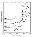
- FIG. 1 shows a graph showing the relationship between the X-ray photon energy and intensity obtained by NEXAFS for the boron-doped diamonds obtained in Examples 1 and 2 and Comparative Examples 1 and 2. Further, the peak intensity A of the diamond core exonton located in the range of X-ray photon energy 288 eV to 290 eV and the peak intensity area B in the range of X-ray photon energy 286.2 eV to 288.5 eV obtained from these graphs are shown. Values and B / A values are shown in Table 2 (Examples 1, 2, 4 and Comparative Examples 1, 2).
- the surfaces of the boron-doped diamond obtained in Examples 2 and 3 and Comparative Example 2 were washed by hot mixed acid treatment, and then transported to a chamber for NEXAFS analysis.
- the surface of the boron-doped diamond was irradiated with an X-ray beam under an ultra-high vacuum, and scanned in the range of X-ray photon energy of 175 eV to 220 eV.
- the faint light emitted from the sample surface was detected by a fluorescence detector.
- I S / I 0 obtained by normalizing the detection spectrum with the incident energy is the NEXAFS spectrum.
- the incident X-ray angle was 90 ° (right angle) with respect to the sample, the incident X-ray energy was 1 pA (at 175 eV), and the analysis chamber vacuum was 8.0 ⁇ 10 ⁇ 8 Pa.
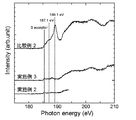
- the thermal mixed acid treatment is a treatment in which boron-doped diamond is boiled and washed in a mixed solution of sulfuric acid and nitric acid at 250 ° C. to 450 ° C. The results are shown in Table 3 and FIG.
- the boron-doped diamond obtained in Examples 2 and 3 has substantially no peaks at the positions of 187.1 eV and 189.1 eV, It can be seen that a cluster in which boron atoms are substantially bonded to each other is not included in the boron-doped single crystal diamond.
Landscapes
- Chemical & Material Sciences (AREA)
- Organic Chemistry (AREA)
- Inorganic Chemistry (AREA)
- Engineering & Computer Science (AREA)
- Materials Engineering (AREA)
- Metallurgy (AREA)
- Chemical Kinetics & Catalysis (AREA)
- General Chemical & Material Sciences (AREA)
- Crystallography & Structural Chemistry (AREA)
- Mechanical Engineering (AREA)
- Life Sciences & Earth Sciences (AREA)
- General Life Sciences & Earth Sciences (AREA)
- Geology (AREA)
- Crystals, And After-Treatments Of Crystals (AREA)
- Carbon And Carbon Compounds (AREA)
- Chemical Vapour Deposition (AREA)
Abstract
ホウ素を高濃度で含んでいるにも拘わらず、電気抵抗値が小さい、ホウ素ドープダイヤモンドを提供する。 ダイヤモンドにホウ素がドープされている、ホウ素ドープダイヤモンドであって、 二次イオン質量分析法で測定したホウ素濃度が、1×1019cm-3超、1×1022cm-3以下の範囲にあり、 X線吸収微細構造解析(NEXAFS)によって測定される、X線光子エネルギー288eV~290eVの範囲に位置するダイヤモンドコアエキシントンのピーク強度Aと、X線光子エネルギー286.2eV~288.5eVの範囲におけるピーク強度面積Bとの比(B/A)が、0.30以下である、ホウ素ドープダイヤモンド。
Description
本発明は、ダイヤモンドにホウ素がドープされた、ホウ素ドープダイヤモンドに関する。
ダイヤモンドは、高絶縁破壊電界(>10MV/cm)、高速キャリア移動度(電子:4500cm2/Vs、正孔:3800cm2/Vs)、物質中最高の熱伝導率(22W/cmK)等の優れた物性を有しており、さらに、化学的安定性及び耐放射線性にも優れているため、高温・極限環境下で動作するパワーデバイス材料としての応用が期待されている。
ダイヤモンドをパワーデバイス材料などに応用するためには、ホウ素などの不純物をダイヤモンド結晶中に高濃度でドープして、ダイヤモンド結晶を低抵抗化する必要がある。ダイヤモンド結晶中にホウ素などの不純物をドープする方法としては、マイクロ波CVD法等が広く使用されている。
例えば、特許文献1には、炭素を主成分とする半導体ダイヤモンドであって、窒素原子及びホウ素原子を含有し、その濃度がどちらも1000ppm以上であることを特徴とする半導体ダイヤモンドが記載されている。特許文献1に開示された方法によれば、マイクロ波CVD法を用い、窒素源、ホウ素源、及び炭素源を含む原料ガスを製膜することにより、ホウ素がドープされた、単結晶構造を有するホウ素ドープダイヤモンド膜が得られるとされている。
例えば特許文献1に記載されたような方法を用いることにより、ホウ素がドープされた、ホウ素ドープ単結晶ダイヤモンドが得られると考えられる。しかしながら、従来のホウ素ドープ単結晶ダイヤモンドは、ホウ素を高濃度(例えば、ホウ素濃度が1×1019cm-3超)で含有させると、置換原子位置以外のサイトにホウ素が組み込まれ、電気抵抗値が大きくなるという問題がある。
本発明は、ホウ素を高濃度で含んでいるにも拘わらず、電気抵抗値の小さいホウ素ドープダイヤモンドを提供することを主な目的とする。
本発明者らは、上記のような課題を解決すべく鋭意検討を行った。その結果、ダイヤモンドにホウ素がドープされているホウ素ドープダイヤモンドにおいて、二次イオン質量分析法で測定したホウ素濃度が、1×1019cm-3超、1×1022cm-3以下の範囲にあり、X線吸収微細構造解析(NEXAFS)によって測定される、X線光子エネルギー288eV~290eVの範囲に位置するダイヤモンドコアエキシントンのピーク強度Aと、X線光子エネルギー286.2eV~288.5eVの範囲におけるピーク強度面積Bとの比(B/A)が、0.30以下であるホウ素ドープダイヤモンドは、高濃度のホウ素を含んでいるにも拘わらず、電気抵抗値が非常に低いことを見出した。
さらに、本発明者らは、ホウ素ドープダイヤモンドにおいて、二次イオン質量分析法で測定したホウ素濃度が、1×1019cm-3超、1×1022cm-3以下の範囲にあり、X線吸収微細構造解析(NEXAFS)によって測定される、ホウ素原子の1s軌道から外殻へのX線吸収スペクトルにおいて、ホウ素原子同士が結合したクラスターが存在することを示す187.1eV及び189.1eVの位置にピークを実質的に有していないホウ素ドープダイヤモンドについても、高濃度のホウ素を含んでいるにも拘わらず、電気抵抗値が非常に低いことを見出した。
そして、本発明者等は、これらのホウ素ドープダイヤモンドは、熱フィラメントCVD法を採用することにより、好適に製造できることを見出した。本発明は、これらの知見に基づいて、さらに検討を重ねることにより完成された発明である。
すなわち、本発明は、下記に掲げる態様の発明を提供する。
項1. ダイヤモンドにホウ素がドープされている、ホウ素ドープダイヤモンドであって、
二次イオン質量分析法で測定したホウ素濃度が、1×1019cm-3超、1×1022cm-3以下の範囲にあり、
X線吸収微細構造解析(NEXAFS)によって測定される、X線光子エネルギー288eV~290eVの範囲に位置するダイヤモンドコアエキシントンのピーク強度Aと、X線光子エネルギー286.2eV~288.5eVの範囲におけるピーク強度面積Bとの比(B/A)が、0.30以下である、ホウ素ドープダイヤモンド。
項2. X線吸収微細構造解析(NEXAFS)によって測定される、ホウ素原子の1s軌道から外殻へのX線吸収スペクトルにおいて、ホウ素原子同士が結合したクラスターが存在することを示す187.1eV及び189.1eVの位置にピークを実質的に有していない、項1に記載のホウ素ドープダイヤモンド。
項3. ダイヤモンドにホウ素がドープされている、ホウ素ドープダイヤモンドであって、
二次イオン質量分析法で測定したホウ素濃度が、1×1019cm-3超、1×1022cm-3以下の範囲にあり、
X線吸収微細構造解析(NEXAFS)によって測定される、ホウ素原子の1s軌道から外殻へのX線吸収スペクトルにおいて、ホウ素原子同士が結合したクラスターが存在することを示す187.1eV及び189.1eVの位置にピークを実質的に有していない、ホウ素ドープダイヤモンド。
項4. 厚みが0.01μm~1mmの範囲にある、項1~3のいずれかに記載のホウ素ドープダイヤモンド。
項5. 前記ホウ素ドープダイヤモンドの厚みの最大値と最小値との差が、当該最大値の10%以下である、項1~4のいずれかに記載のホウ素ドープダイヤモンド。
項6. 基板の上に形成されている、項1~5のいずれかに記載のホウ素ドープダイヤモンド。
項7. 項1~6のいずれかに記載のホウ素ドープダイヤモンドを含む、電子デバイス。
項1. ダイヤモンドにホウ素がドープされている、ホウ素ドープダイヤモンドであって、
二次イオン質量分析法で測定したホウ素濃度が、1×1019cm-3超、1×1022cm-3以下の範囲にあり、
X線吸収微細構造解析(NEXAFS)によって測定される、X線光子エネルギー288eV~290eVの範囲に位置するダイヤモンドコアエキシントンのピーク強度Aと、X線光子エネルギー286.2eV~288.5eVの範囲におけるピーク強度面積Bとの比(B/A)が、0.30以下である、ホウ素ドープダイヤモンド。
項2. X線吸収微細構造解析(NEXAFS)によって測定される、ホウ素原子の1s軌道から外殻へのX線吸収スペクトルにおいて、ホウ素原子同士が結合したクラスターが存在することを示す187.1eV及び189.1eVの位置にピークを実質的に有していない、項1に記載のホウ素ドープダイヤモンド。
項3. ダイヤモンドにホウ素がドープされている、ホウ素ドープダイヤモンドであって、
二次イオン質量分析法で測定したホウ素濃度が、1×1019cm-3超、1×1022cm-3以下の範囲にあり、
X線吸収微細構造解析(NEXAFS)によって測定される、ホウ素原子の1s軌道から外殻へのX線吸収スペクトルにおいて、ホウ素原子同士が結合したクラスターが存在することを示す187.1eV及び189.1eVの位置にピークを実質的に有していない、ホウ素ドープダイヤモンド。
項4. 厚みが0.01μm~1mmの範囲にある、項1~3のいずれかに記載のホウ素ドープダイヤモンド。
項5. 前記ホウ素ドープダイヤモンドの厚みの最大値と最小値との差が、当該最大値の10%以下である、項1~4のいずれかに記載のホウ素ドープダイヤモンド。
項6. 基板の上に形成されている、項1~5のいずれかに記載のホウ素ドープダイヤモンド。
項7. 項1~6のいずれかに記載のホウ素ドープダイヤモンドを含む、電子デバイス。
本発明によれば、ホウ素を高濃度で含んでいるにも拘わらず、電気抵抗値の小さいホウ素ドープダイヤモンドを提供することができる。
本発明のホウ素ドープダイヤモンドは、ダイヤモンドにホウ素がドープされている、ホウ素ドープダイヤモンドである。本発明において、ホウ素ドープダイヤモンドの結晶構造は、単結晶でもよいし、多結晶でもよい。例えば、ホウ素ドープダイヤモンドを成膜する基板として、単結晶ダイヤモンド基板を用いると、ホウ素ドープ単結晶ダイヤモンドが得られる。また、例えば、多結晶ダイヤモンド基板を用いると、ホウ素ドープ多結晶ダイヤモンドが得られる。なお、ホウ素ドープ多結晶ダイヤモンドの合成には、異種基板(Si、SiC、GaN、WCなど)を用いてもよい。異種基板上に,ダイヤモンド微粒子を用いて所謂「傷つけ処理」を施すことにより、ダイヤモンドの核生成を促し、ホウ素ドープ多結晶ダイヤモンドを成長させることができる。なお、傷つけ処理は、基材によっては不要な場合がある。
本発明のホウ素ドープダイヤモンドにおいては、二次イオン質量分析法で測定したホウ素濃度が、1×1019cm-3超、1×1022cm-3以下の範囲にある。さらに、本発明の第1のホウ素ドープダイヤモンドにおいては、X線吸収微細構造解析(NEXAFS)によって測定される、X線光子エネルギー288eV~290eVの範囲に位置するダイヤモンドコアエキシントンのピーク強度Aと、X線光子エネルギー286.2eV~288.5eVの範囲におけるピーク強度面積Bとの比(B/A)が、0.30以下であることを特徴とする。なお、NEXAFSによる具体的な測定方法は、実施例に記載のとおりである。
従来のホウ素ドープダイヤモンドにおいては、ホウ素濃度が1×1019cm-3超という高濃度になると、ホウ素ドープダイヤモンドに含まれるホウ素原子同士が結合したクラスターが形成され、前記のピーク強度面積比(B/A)が0.30を大きく超えるという特徴を有している。当該ピーク強度面積比(B/A)が0.30を大きく超えると、置換原子位置以外のサイトにホウ素が組み込まれ、電気抵抗値が大きくなるという問題がある。これに対して、本発明の第1のホウ素ドープダイヤモンドにおいては、当該ピーク強度面積比(B/A)が0.30以下であるため、ホウ素濃度が、1×1019cm-3超、1×1022cm-3以下の範囲という高濃度であるにも拘わらず、当該ピーク強度面積比(B/A)が0.30以下であり、ホウ素ドープダイヤモンドに含まれるホウ素原子同士が結合したクラスターが実質的に存在しない。このため、第1のホウ素ドープダイヤモンドにおいては、置換原子位置にホウ素が組み込まれており、電気抵抗値が小さいという特徴を有している。
また、本発明の第1のホウ素ドープダイヤモンドにおいては、X線吸収微細構造解析(NEXAFS)によって測定される、ホウ素原子の1s軌道から外殻へのX線吸収スペクトルにおいて、ホウ素原子同士が結合したクラスターが存在することを示す187.1eV及び189.1eVの位置にピークを実質的に有していないことが好ましい。当該特性を備えるホウ素ドープダイヤモンドにおいても、ホウ素ドープダイヤモンドに含まれるホウ素原子同士が結合したクラスターが実質的に存在せず、置換原子位置にホウ素が組み込まれており、電気抵抗値が小さいという特徴を有している。NEXAFSによる具体的な測定方法は、実施例に記載のとおりである。
なお、前記のNEXAFS測定において、187.1eV及び189.1eVの位置に観測されるピークが、ホウ素ドープダイヤモンド中のホウ素同士が結合したクラスターに起因していることは、例えば"Diamond & Related Materials 39 (2013) 53-57"などに報告されている。
本発明の第2のホウ素ドープダイヤモンドは、二次イオン質量分析法で測定したホウ素濃度が、1×1019cm-3超、1×1022cm-3以下の範囲にあり、X線吸収微細構造解析(NEXAFS)によって測定される、ホウ素原子の1s軌道から外殻へのX線吸収スペクトルにおいて、ホウ素原子同士が結合したクラスターが存在することを示す187.1eV及び189.1eVの位置にピークを実質的に有していないことを特徴としている。前述の第1のホウ素ドープダイヤモンドと同様、第2のホウ素ドープダイヤモンドにおいても、ホウ素ドープダイヤモンドに含まれるホウ素原子同士が結合したクラスターが実質的に存在しないため、置換原子位置にホウ素が組み込まれており、電気抵抗値が小さいという特徴を有している。
本発明のホウ素ドープダイヤモンドの電気抵抗値としては、特に制限されないが、後述の電子デバイスとして好適に用いる観点からは、例えば温度25℃における電気抵抗値としては、好ましくは30mΩcm以下、より好ましくは25mΩcm以下、さらに好ましくは5mΩcm以下が挙げられる。なお、電気抵抗値の下限値としては、通常、0.1mΩcm程度である。電気抵抗値は、ホール効果によって測定した値であり、具体的な測定条件は、後述の実施例に記載の通りである。
本発明のホウ素ドープダイヤモンドは、ダイヤモンドの炭素原子の一部がホウ素原子によって置換された結晶構造を有している。ホウ素ドープダイヤモンドにおいて、ホウ素以外の不純物(例えば、リン)が含まれていてもよい。ホウ素以外の不純物は、1種類単独で含まれていてもよいし、2種類以上含まれていてもよい。
本発明のホウ素ドープダイヤモンドの製造方法としては、例えば、熱フィラメントCVD法により好適に製造することができる。なお、従来、ホウ素ドープダイヤモンドの合成法として、熱フィラメントCVD法を用いることも考えられたが、例えば単結晶構造を有するホウ素ドープダイヤモンドを合成しようとすると、フィラメントを構成する金属元素(例えば、タングステンフィラメントを構成するタングステン)もドープされるため、単結晶構造を備えるホウ素ドープダイヤモンドについては、好適に製造することはできないと考えられた。特に、ホウ素を高濃度でドープする場合には、単結晶構造を備えるホウ素ドープダイヤモンドが合成できるとは考えられなかった。
ところが、本発明者らが検討を重ねたところ、意外にも、熱フィラメントCVD法を採用することにより、単結晶構造を有するホウ素ドープダイヤモンドが好適に得られることを見出した。さらに、本発明者らは、熱フィラメントCVD法を採用することにより、長時間にわたる合成によっても、高濃度のホウ素(例えば、二次イオン質量分析法で測定したホウ素濃度が1×1019cm-3超)がドープされたホウ素ドープダイヤモンドを合成することができ、チャンバー内に煤が堆積せず、単結晶構造の結晶品質に優れたホウ素ドープダイヤモンドが得られることを見出した。また、ホウ素ドープダイヤモンドの厚膜化、大面積化も可能であることを見出した。
例えば、熱フィラメントCVD法により製造されたホウ素ドープダイヤモンド中には、通常、熱フィラメントを構成する金属元素(例えば、後述のタングステンなど)が含まれている。一方、マイクロ波CVD法により合成されたホウ素ドープダイヤモンドには、このような金属元素は含まれない。
なお、本発明のホウ素ドープダイヤモンドには、上記のようなホウ素に加えて、当該ホウ素とは異なる金属元素を含んでいてもよい。熱フィラメントCVD法により本発明のホウ素ドープダイヤモンドを製造した場合には、通常、フィラメントを構成する金属元素がホウ素ドープダイヤモンド中に含まれる。金属元素の具体例としては、タングステン、タンタル、レニウム、ルテニウム等が挙げられる。
ホウ素ドープダイヤモンドに金属元素が含まれる場合、金属元素の濃度としては、特に制限されないが、例えば1×10¹⁶~1×1020cm-3程度の範囲が挙げられる。なお、ホウ素ドープダイヤモンドにおける金属元素の濃度は、二次イオン質量分析法(SIMS)により測定した値である。
本発明のホウ素ドープダイヤモンドの厚みとしては、特に制限されないが、例えば0.01μm~1mm程度、より好ましくは0.1~500μm程度が挙げられる。例えば、マイクロ波CVD法によってホウ素ドープダイヤモンドを合成する場合、チャンバー内に煤が発生しやすいため、例えば0.1μm~1mm程度の厚膜とすることが可能なホウ素濃度としては、1.2×1020cm-3が限界であるとされている(例えば、Appl.Phys.Lett.100(2012)122109を参照)。一方、熱フィラメントCVD法により製造すれば、ホウ素濃度が1×1019cm-3超である場合にも、ホウ素ドープダイヤモンドの厚みを0.1μm~1mm程度とすることが可能である。
本発明のホウ素ドープダイヤモンドの厚みの最大値と最小値との差は、当該最大値の10%以下であることが好ましく、5%以下であることがより好ましい。熱フィラメントCVD法によりホウ素ドープダイヤモンドを合成すれば、このような厚み均一性の高いホウ素ドープダイヤモンドとすることもできる。
本発明のホウ素ドープダイヤモンドは、例えば、熱フィラメントCVD法などを用いて基板の上に形成することができるため、基板の上に形成された形態を有していてもよい。基板の具体例としては、単結晶ダイヤモンド、多結晶ダイヤモンド、3C炭化シリコン、イリジウム、プラチナなどが挙げられる。
本発明のホウ素ドープダイヤモンドは、ホウ素を上記のような高濃度で含有しており、さらに、結晶格子歪みが小さく、電気抵抗値が小さいことから、ダイオード、トランジスタなどの電子デバイス用材料(特に、パワーデバイス用材料)として好適である。すなわち、本発明によれば、ホウ素ドープダイヤモンドを含む電子デバイスを提供することができる。本発明のホウ素ドープダイヤモンドを利用した電子デバイスとしては、例えば、ショットキーダイオード、PN接合ダイオード、電界効果トランジスタ、深紫外線ディテクター、電子エミッタなどが挙げられる。
本発明のホウ素ドープダイヤモンドを熱フィラメントCVD法で製造する際の製造方法としては、例えば、以下の工程を備える方法が挙げられる。
工程(1):基板及びフィラメントが配置された真空容器中に、炭素源及びホウ素源を含むキャリアガスを導入する工程
工程(2):キャリアガスをフィラメントで加熱して、ホウ素を含むダイヤモンドを基板上に製膜する製膜工程
工程(1):基板及びフィラメントが配置された真空容器中に、炭素源及びホウ素源を含むキャリアガスを導入する工程
工程(2):キャリアガスをフィラメントで加熱して、ホウ素を含むダイヤモンドを基板上に製膜する製膜工程
工程(1)において、真空容器中に配置するフィラメントを構成する金属としては、フィラメントを構成できるものであれば特に制限されない。金属元素の具体例としては、タングステン、タンタル、レニウム、ルテニウム等が挙げられ、これらの中でもタングステンが好ましい。金属元素は、1種類単独で使用してもよいし、2種類以上を組み合わせて使用してもよい。
工程(1)において、真空容器中に配置する基板としては、後述の工程(2)において、キャリアガスに含まれる炭素源とホウ素とが基板上に製膜されて、ダイヤモンドの結晶構造を有するホウ素ドープダイヤモンドを成長させることができるものであれば、特に制限されない。基板の具体例としては、単結晶ダイヤモンド、多結晶ダイヤモンド、3C炭化シリコン、イリジウム、プラチナなどが挙げられる。
工程(1)においては、真空容器中を真空状態とした後、炭素源及びホウ素源を含むキャリアガスを導入する。炭素源としては、ダイヤモンドを形成できるものであれば特に制限されず、例えば、メタンなどが挙げられる。炭素源は、1種類単独で使用してもよいし、2種類以上を組み合わせて使用してもよい。また、ホウ素源としては、ホウ素としてダイヤモンド中にドープされて、ダイヤモンドの結晶構造を保持できるものであれば、特に制限されず、好ましくはトリメチルボロン、ジボランなどが挙げられる。ホウ素源は、1種類単独で使用してもよいし、2種類以上を組み合わせて使用してもよい。
キャリアガスとしては、特に制限されず、例えば、水素ガスを使用することができる。キャリアガス中における炭素源の濃度としては、好ましくは0.5~5.0体積%程度、より好ましくは1.0~3.0体積%程度が挙げられる。また、キャリアガス中における炭素源に対するホウ素源の濃度としては、ホウ素ドープダイヤモンド中に含ませるホウ素濃度に応じて適宜設定すればよい。例えば、ホウ素ドープダイヤモンドにおけるホウ素の濃度を1×1019cm-3超、1×1022cm-3以下とする観点からは、キャリアガス中における炭素源に対するホウ素源の濃度としては、好ましくは100ppm以上、より好ましくは1000~20000ppm程度、さらに好ましくは5000~10000ppm程度が挙げられる。
工程(2)においては、キャリアガスをフィラメントで加熱して、ホウ素ドープダイヤモンドを基板の上に製膜する製膜工程を行う。フィラメントの加熱温度は、使用するフィラメントを構成する金属元素の種類や、ホウ素ドープダイヤモンド中に含有させるホウ素の濃度に応じて、適宜設定すればよく、好ましくは2000~2400℃程度、より好ましくは2000~2200℃程度が挙げられる。
工程(2)における真空容器内の全圧としては、特に制限されず、例えば10~100Torr程度、より好ましくは10~80Torr程度が挙げられる。
工程(2)における基板の温度としては、特に制限されず、例えば700~1100℃程度、より好ましくは700~900℃程度が挙げられる。
工程(2)における製膜時間は、目的とする厚み等に応じて適宜選択すればよく、通常3~50時間程度である。
工程(2)の製膜工程においては、ダイヤモンドにおけるホウ素の濃度を1×10¹⁹超、1×1022cm-3以下とすることができる。前述の通り、本発明のホウ素ドープダイヤモンドの製造方法においては、キャリアガス中における炭素源に対するホウ素源の濃度を、好ましくは100ppm以上とすることにより、ホウ素ドープダイヤモンドにおけるホウ素の濃度を1×1019cm-3超、1×1022cm-3以下となるように調整することができる。
本発明のホウ素ドープダイヤモンドの製造方法において、ホウ素を高濃度でドープする場合、キャリアガス中における炭素源の濃度を0.1~5.0体積%、真空容器内の全圧を10~80Torr、基板の温度を700~900℃とした上で、基板の前処理におけるオフ角を0.5~3°に設定することにより、1×1019cm-3超という高濃度のホウ素を含むホウ素ドープダイヤモンドを、特に好適に製造することができる。
以上の工程(1)及び工程(2)により、本発明のホウ素ドープダイヤモンドを好適に製造することができる。
以下に、実施例及び比較例を示して本発明を詳細に説明する。ただし、本発明は、実施例に限定されない。
<実施例1-3>
単結晶ダイヤモンド基板(100)の表面上に、熱フィラメント化学気相成長法(熱フィラメントCVD法)によりホウ素ドープ単結晶ダイヤモンドを製膜した。各実施例における製膜条件は以下の通りである。
(製膜条件)
・キャリアガス:水素97体積%、メタン3体積%(炭素源)であり、メタンに対するトリメチルボロン(ホウ素源)の体積濃度(気相中[B/C]gas、ppm)は、それぞれ表1に記載の通りである。
・全圧:30Torr
・フィラメント材料:タングステン純度99.95%
・フィラメント温度:2200℃
・基板温度:1100℃
・基板サイズ:3mm×3mm
・製膜時間:10時間
・ホウ素ドープ単結晶ダイヤモンドの膜厚:それぞれ、表1の通りである。
・基板前処理のオフ角:2.5°
単結晶ダイヤモンド基板(100)の表面上に、熱フィラメント化学気相成長法(熱フィラメントCVD法)によりホウ素ドープ単結晶ダイヤモンドを製膜した。各実施例における製膜条件は以下の通りである。
(製膜条件)
・キャリアガス:水素97体積%、メタン3体積%(炭素源)であり、メタンに対するトリメチルボロン(ホウ素源)の体積濃度(気相中[B/C]gas、ppm)は、それぞれ表1に記載の通りである。
・全圧:30Torr
・フィラメント材料:タングステン純度99.95%
・フィラメント温度:2200℃
・基板温度:1100℃
・基板サイズ:3mm×3mm
・製膜時間:10時間
・ホウ素ドープ単結晶ダイヤモンドの膜厚:それぞれ、表1の通りである。
・基板前処理のオフ角:2.5°
<実施例4>
傷つけ処理を行ったSi基板の表面上に、熱フィラメント化学気相成長法(熱フィラメントCVD法)によりホウ素ドープ多結晶ダイヤモンドを製膜した。製膜条件は以下の通りである。
(製膜条件)
・キャリアガス:水素97体積%、メタン3体積%(炭素源)であり、メタンに対するトリメチルボロン(ホウ素源)の体積濃度(気相中[B/C]gas、ppm)は、表1に記載の通りである。
・全圧:30Torr
・フィラメント材料:タングステン純度99.95%
・フィラメント温度:2200℃
・基板温度:1100℃
・基板サイズ:10mm×10mm
・製膜時間:5時間
・ホウ素ドープ多結晶ダイヤモンドの膜厚:表1の通りである。
傷つけ処理を行ったSi基板の表面上に、熱フィラメント化学気相成長法(熱フィラメントCVD法)によりホウ素ドープ多結晶ダイヤモンドを製膜した。製膜条件は以下の通りである。
(製膜条件)
・キャリアガス:水素97体積%、メタン3体積%(炭素源)であり、メタンに対するトリメチルボロン(ホウ素源)の体積濃度(気相中[B/C]gas、ppm)は、表1に記載の通りである。
・全圧:30Torr
・フィラメント材料:タングステン純度99.95%
・フィラメント温度:2200℃
・基板温度:1100℃
・基板サイズ:10mm×10mm
・製膜時間:5時間
・ホウ素ドープ多結晶ダイヤモンドの膜厚:表1の通りである。
<比較例1>
高温高圧法で作製された市販のホウ素ドープ単結晶ダイヤモンド基板(TISNCM社製、type-IIb基板,面方位 (100)、ホウ素濃度:約1020cm-3、基板厚さ:300μm)を用いた。
高温高圧法で作製された市販のホウ素ドープ単結晶ダイヤモンド基板(TISNCM社製、type-IIb基板,面方位 (100)、ホウ素濃度:約1020cm-3、基板厚さ:300μm)を用いた。
<比較例2>
単結晶ダイヤモンド基板(100)の表面上に、マイクロ波CVD法によりホウ素ドープ単結晶ダイヤモンドを製膜した。製膜条件は以下の通りである。
(製膜条件)
・キャリアガス:水素97体積%、メタン3体積%(炭素源)であり、メタンに対するトリメチルボロン(ホウ素源)の体積濃度(気相中[B/C]gas、ppm)は、10000体積%
・全圧:80Torr
・基板温度:1000℃
・基板サイズ:3mm×3mm
・製膜時間:10時間
・ホウ素ドープ単結晶ダイヤモンドの膜厚:1μm
・基板前処理のオフ角:2.5°
単結晶ダイヤモンド基板(100)の表面上に、マイクロ波CVD法によりホウ素ドープ単結晶ダイヤモンドを製膜した。製膜条件は以下の通りである。
(製膜条件)
・キャリアガス:水素97体積%、メタン3体積%(炭素源)であり、メタンに対するトリメチルボロン(ホウ素源)の体積濃度(気相中[B/C]gas、ppm)は、10000体積%
・全圧:80Torr
・基板温度:1000℃
・基板サイズ:3mm×3mm
・製膜時間:10時間
・ホウ素ドープ単結晶ダイヤモンドの膜厚:1μm
・基板前処理のオフ角:2.5°
[ホウ素濃度の測定]
上記の実施例1-4,比較例1-2で得られたホウ素ドープダイヤモンドに含まれるホウ素濃度を二次イオン質量分析法(SIMS、Cs+イオン加速電圧15.0kV)により測定した。結果を表2,3に示す。
上記の実施例1-4,比較例1-2で得られたホウ素ドープダイヤモンドに含まれるホウ素濃度を二次イオン質量分析法(SIMS、Cs+イオン加速電圧15.0kV)により測定した。結果を表2,3に示す。
[X線吸収微細構造解析(C1s)]
上記の実施例1,2,4及び比較例1,2で得られたホウ素ドープダイヤモンドについて、X線吸収微細構造解析(NEXAFS)を行った。一般に、ダイヤモンドのNEXAFSによる評価においては、ホストエレメントの炭素(カーボン)の1sから外殻へのX線吸収スペクトルが利用される。すなわち、炭素原子の吸収端近傍(275eV~345eV)でX線光子エネルギーをスキャンし、吸収過程におけるエネルギー損失分を検出することでスペクトルが得られる。このときの検出方法としては、超高真空中で測定が可能な電子収量法(Total electron yield:TEY)または蛍光収量法(Fluorescence yield: FY)を通常用いることができる。ここでは、ホウ素ドープダイヤモンドに含まれるホウ素原子同士が結合したクラスターを確認するため、TEY法を用いた。
上記の実施例1,2,4及び比較例1,2で得られたホウ素ドープダイヤモンドについて、X線吸収微細構造解析(NEXAFS)を行った。一般に、ダイヤモンドのNEXAFSによる評価においては、ホストエレメントの炭素(カーボン)の1sから外殻へのX線吸収スペクトルが利用される。すなわち、炭素原子の吸収端近傍(275eV~345eV)でX線光子エネルギーをスキャンし、吸収過程におけるエネルギー損失分を検出することでスペクトルが得られる。このときの検出方法としては、超高真空中で測定が可能な電子収量法(Total electron yield:TEY)または蛍光収量法(Fluorescence yield: FY)を通常用いることができる。ここでは、ホウ素ドープダイヤモンドに含まれるホウ素原子同士が結合したクラスターを確認するため、TEY法を用いた。
NEXAFSにおいて、実施例3-5及び比較例1,2で得られたホウ素ドープダイヤモンドの表面を熱混酸処理によって洗浄したのち、NEXAFS分析用のチャンバーに輸送した。次に、ホウ素ドープダイヤモンドの表面に、超高真空下でX線ビームを照射し、X線光子エネルギー275eV~345eVの範囲でスキャンした。このとき、光子エネルギー強度をI0とし、前述のTEY法で測定されるX線吸収電流をISとした。検出スペクトルを入射エネルギーで規格化したIS/I0が、NEXAFSスペクトルである。入射X線角度は試料に対して90°(直角)、入射X線エネルギーは3pA(275eVにて)、分析室真空度は8.0×10-8Paとした。また、熱混酸処理は、250℃~450℃の硫酸と硝酸の混合液中でホウ素ドープダイヤモンドを煮沸洗浄する処理である。
このようにして得られたスペクトルは、種々の要因でバックグラウンドを含んでいる。このため、X線光子エネルギー275eV~345eVの範囲のスペクトルを基準とし、Victoreen-Fit法によりバックグラウンド補正を行い、真のスペクトルを抽出した。真のスペクトルから、X線光子エネルギー288eV~290eVの範囲に位置するダイヤモンドコアエキシントンのピーク強度Aと、X線光子エネルギー286.2eV~288.5eVの範囲におけるピーク強度面積Bを求め、BとAの比(B/A)を算出した。X線光子エネルギー範囲286.2eV~288.5eVには、ホウ素ドープダイヤモンドにおいて、ホウ素原子同士が結合したクラスターのピークが表れるため、BとAの比(B/A)の値により、当該クラスターの有無を判定することができる。
実施例1,2及び比較例1,2で得られたホウ素ドープダイヤモンドについて、NEXAFSによって得られたX線光子エネルギーと強度との関係を示すグラフを図1に示す。また、これらのグラフから得られたX線光子エネルギー288eV~290eVの範囲に位置するダイヤモンドコアエキシントンのピーク強度Aと、X線光子エネルギー286.2eV~288.5eVの範囲におけるピーク強度面積Bの値、B/Aの値を表2に示す(実施例1,2,4及び比較例1,2)。
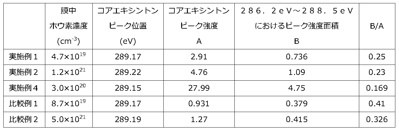
表2及び図1に示されるグラフから明らかな通り、実施例1,2,4で得られたホウ素ドープダイヤモンドにおいては、B/Aの値が0.30以下と小さく、実質的にホウ素原子同士が結合したクラスターがホウ素ドープ単結晶ダイヤモンド中に含まれていないことが分かる。
[X線吸収微細構造解析(B1s)]
上記の実施例2,3及び比較例2で得られたホウ素ドープダイヤモンドについて、X線吸収微細構造解析(NEXAFS)を行った。ホウ素原子の吸収端近傍(175eV~220eV)でX線光子エネルギーをスキャンし、吸収過程におけるエネルギー損失分を検出することでスペクトルが得られる。このときの検出方法としては、超高真空中で測定が可能な電子収量法(Total electron yield:TEY)または蛍光収量法(Fluorescence yield: FY)を通常用いることができる。ここでは、ホウ素ドープダイヤモンドに含まれるホウ素原子同士が結合したクラスターを高感度に測定するため、FY法を用いた。
上記の実施例2,3及び比較例2で得られたホウ素ドープダイヤモンドについて、X線吸収微細構造解析(NEXAFS)を行った。ホウ素原子の吸収端近傍(175eV~220eV)でX線光子エネルギーをスキャンし、吸収過程におけるエネルギー損失分を検出することでスペクトルが得られる。このときの検出方法としては、超高真空中で測定が可能な電子収量法(Total electron yield:TEY)または蛍光収量法(Fluorescence yield: FY)を通常用いることができる。ここでは、ホウ素ドープダイヤモンドに含まれるホウ素原子同士が結合したクラスターを高感度に測定するため、FY法を用いた。
実施例2,3及び比較例2で得られたホウ素ドープダイヤモンドの表面を熱混酸処理によって洗浄したのち、NEXAFS分析用のチャンバーに輸送した。次に、ホウ素ドープダイヤモンドの表面に、超高真空下でX線ビームを照射し、X線光子エネルギー175eV~220eVの範囲でスキャンした。このとき、試料表面から放出される微弱光を蛍光検出器にて検出した。検出スペクトルを入射エネルギーで規格化したIS/I0が、NEXAFSスペクトルである。入射X線角度は試料に対して90°(直角)、入射X線エネルギーは1pA(175 eVにて)、分析室真空度は8.0×10⁻⁸Paとした。また、熱混酸処理は、250℃~450℃の硫酸と硝酸の混合液中でホウ素ドープダイヤモンドを煮沸洗浄する処理である。結果を表3及び図2に示す。
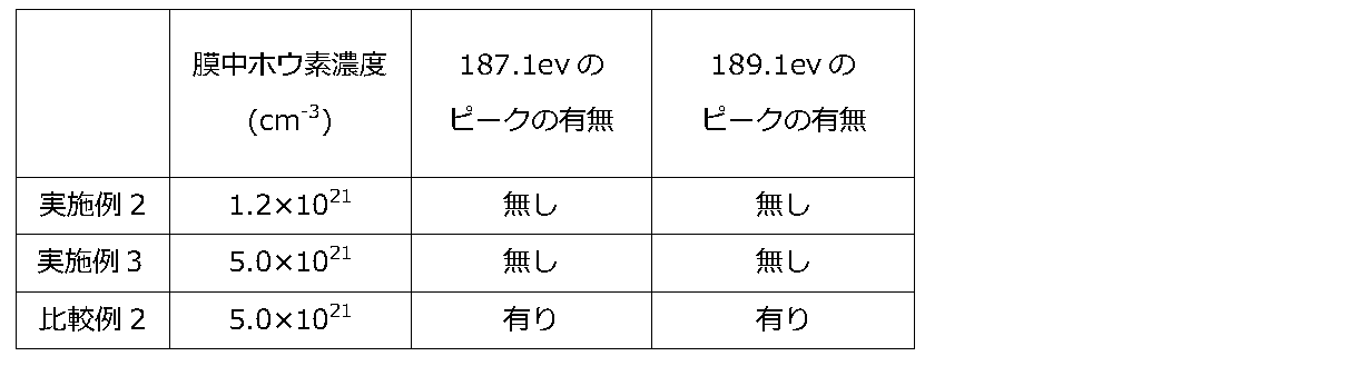
表3及び図2に示されるグラフから明らかな通り、実施例2,3で得られたホウ素ドープダイヤモンドにおいては、187.1eV及び189.1eVの位置にピークを実質的に有しておらず、実質的にホウ素原子同士が結合したクラスターがホウ素ドープ単結晶ダイヤモンド中に含まれていないことが分かる。
[電気抵抗値の測定]
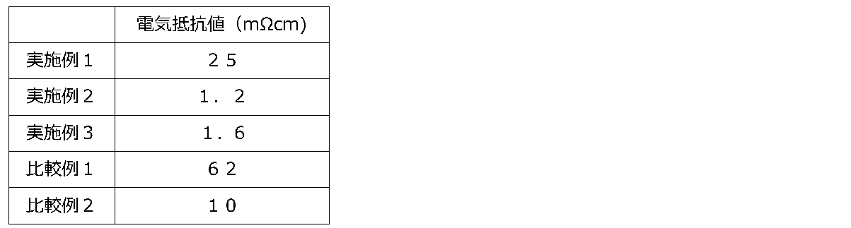
上記の実施例1-3及び比較例1-2で得られたホウ素ドープダイヤモンドの電気抵抗値を、van der Pauw法によるホール効果(25℃)により測定した。結果を表4に示す。
上記の実施例1-3及び比較例1-2で得られたホウ素ドープダイヤモンドの電気抵抗値を、van der Pauw法によるホール効果(25℃)により測定した。結果を表4に示す。
Claims (7)
- ダイヤモンドにホウ素がドープされている、ホウ素ドープダイヤモンドであって、
二次イオン質量分析法で測定したホウ素濃度が、1×1019cm-3超、1×1022cm-3以下の範囲にあり、
X線吸収微細構造解析(NEXAFS)によって測定される、X線光子エネルギー288eV~290eVの範囲に位置するダイヤモンドコアエキシントンのピーク強度Aと、X線光子エネルギー286.2eV~288.5eVの範囲におけるピーク強度面積Bとの比(B/A)が、0.30以下である、ホウ素ドープダイヤモンド。 - X線吸収微細構造解析(NEXAFS)によって測定される、ホウ素原子の1s軌道から外殻へのX線吸収スペクトルにおいて、ホウ素原子同士が結合したクラスターが存在することを示す187.1eV及び189.1eVの位置にピークを実質的に有していない、請求項1に記載のホウ素ドープダイヤモンド。
- ダイヤモンドにホウ素がドープされている、ホウ素ドープダイヤモンドであって、
二次イオン質量分析法で測定したホウ素濃度が、1×1019cm-3超、1×1022cm-3以下の範囲にあり、
X線吸収微細構造解析(NEXAFS)によって測定される、ホウ素原子の1s軌道から外殻へのX線吸収スペクトルにおいて、ホウ素原子同士が結合したクラスターが存在することを示す187.1eV及び189.1eVの位置にピークを実質的に有していない、ホウ素ドープダイヤモンド。 - 厚みが0.01μm~1mmの範囲にある、請求項1~3のいずれかに記載のホウ素ドープダイヤモンド。
- 前記ホウ素ドープダイヤモンドの厚みの最大値と最小値との差が、当該最大値の10%以下である、請求項1~4のいずれかに記載のホウ素ドープダイヤモンド。
- 基板の上に形成されている、請求項1~5のいずれかに記載のホウ素ドープダイヤモンド。
- 請求項1~6のいずれかに記載のホウ素ドープダイヤモンドを含む、電子デバイス。
Applications Claiming Priority (2)
| Application Number | Priority Date | Filing Date | Title |
|---|---|---|---|
| JP2016141306A JP7023477B2 (ja) | 2016-07-19 | 2016-07-19 | ホウ素ドープダイヤモンド |
| JP2016-141306 | 2016-07-19 |
Publications (1)
| Publication Number | Publication Date |
|---|---|
| WO2018016404A1 true WO2018016404A1 (ja) | 2018-01-25 |
Family
ID=60992065
Family Applications (1)
| Application Number | Title | Priority Date | Filing Date |
|---|---|---|---|
| PCT/JP2017/025473 Ceased WO2018016404A1 (ja) | 2016-07-19 | 2017-07-13 | ホウ素ドープダイヤモンド |
Country Status (2)
| Country | Link |
|---|---|
| JP (1) | JP7023477B2 (ja) |
| WO (1) | WO2018016404A1 (ja) |
Cited By (1)
| Publication number | Priority date | Publication date | Assignee | Title |
|---|---|---|---|---|
| CN112456485A (zh) * | 2020-09-24 | 2021-03-09 | 上海江信超硬材料有限公司 | 一种掺杂硼元素的金刚石微粉制备方法 |
Families Citing this family (3)
| Publication number | Priority date | Publication date | Assignee | Title |
|---|---|---|---|---|
| CA3134679A1 (en) | 2019-03-26 | 2020-10-01 | Daicel Corporation | Explosive composition and method for manufacturing same, and method for manufacturing heteroatom-doped nanodiamond |
| WO2021075358A1 (ja) * | 2019-10-18 | 2021-04-22 | 住友電工ハードメタル株式会社 | ダイヤモンド被覆工具 |
| KR102512743B1 (ko) * | 2020-12-18 | 2023-03-22 | 주식회사 케이디티다이아몬드 | 다이아몬드 합성용 마이크로파 플라즈마 cvd 장치 |
Citations (4)
| Publication number | Priority date | Publication date | Assignee | Title |
|---|---|---|---|---|
| JPH08225395A (ja) * | 1994-11-30 | 1996-09-03 | Eastman Kodak Co | ホウ素ドープされたダイヤモンドの製造方法 |
| WO2004104272A1 (ja) * | 2003-05-26 | 2004-12-02 | Sumitomo Electric Industries, Ltd. | ダイヤモンド被覆電極及びその製造方法 |
| JP2012176889A (ja) * | 2012-05-10 | 2012-09-13 | Apollo Diamond Inc | 合成ダイヤモンドを生成するためのシステム及び方法 |
| JP2016213409A (ja) * | 2015-05-13 | 2016-12-15 | 国立研究開発法人産業技術総合研究所 | 不純物ドープダイヤモンド及びその製造方法 |
-
2016
- 2016-07-19 JP JP2016141306A patent/JP7023477B2/ja active Active
-
2017
- 2017-07-13 WO PCT/JP2017/025473 patent/WO2018016404A1/ja not_active Ceased
Patent Citations (4)
| Publication number | Priority date | Publication date | Assignee | Title |
|---|---|---|---|---|
| JPH08225395A (ja) * | 1994-11-30 | 1996-09-03 | Eastman Kodak Co | ホウ素ドープされたダイヤモンドの製造方法 |
| WO2004104272A1 (ja) * | 2003-05-26 | 2004-12-02 | Sumitomo Electric Industries, Ltd. | ダイヤモンド被覆電極及びその製造方法 |
| JP2012176889A (ja) * | 2012-05-10 | 2012-09-13 | Apollo Diamond Inc | 合成ダイヤモンドを生成するためのシステム及び方法 |
| JP2016213409A (ja) * | 2015-05-13 | 2016-12-15 | 国立研究開発法人産業技術総合研究所 | 不純物ドープダイヤモンド及びその製造方法 |
Cited By (1)
| Publication number | Priority date | Publication date | Assignee | Title |
|---|---|---|---|---|
| CN112456485A (zh) * | 2020-09-24 | 2021-03-09 | 上海江信超硬材料有限公司 | 一种掺杂硼元素的金刚石微粉制备方法 |
Also Published As
| Publication number | Publication date |
|---|---|
| JP2018012612A (ja) | 2018-01-25 |
| JP7023477B2 (ja) | 2022-02-22 |
Similar Documents
| Publication | Publication Date | Title |
|---|---|---|
| CN104185697B (zh) | 单晶cvd合成金刚石材料 | |
| Teraji et al. | Growth of high-quality homoepitaxial CVD diamond films at high growth rate | |
| JP2008505833A (ja) | 低ドーピング半絶縁性SiC結晶と方法 | |
| JP7023477B2 (ja) | ホウ素ドープダイヤモンド | |
| Chicot et al. | Electronic and physico-chemical properties of nanometric boron delta-doped diamond structures | |
| Ohmagari et al. | Characterization of free-standing single-crystal diamond prepared by hot-filament chemical vapor deposition | |
| Zebardastan et al. | High quality epitaxial graphene on 4H-SiC by face-to-face growth in ultra-high vacuum | |
| JP6635675B2 (ja) | 不純物ドープダイヤモンド及びその製造方法 | |
| Ohta et al. | Total photoelectron yield spectroscopy of energy distribution of electronic states density at GaN surface and SiO2/GaN interface | |
| Turner et al. | Direct imaging of boron segregation at dislocations in B: diamond heteroepitaxial films | |
| Shammas et al. | In situ photoelectron spectroscopic characterization of c-BN films deposited via plasma enhanced chemical vapor deposition employing fluorine chemistry | |
| Pinault‐Thaury et al. | Electrical activity of (100) n‐type diamond with full donor site incorporation of phosphorus | |
| JP2012176889A (ja) | 合成ダイヤモンドを生成するためのシステム及び方法 | |
| Kono et al. | Imaging of diamond defect sites by electron-beam-induced current | |
| US20250154647A1 (en) | SiC FORMED BODY AND METHOD FOR PRODUCING SiC FORMED BODY | |
| Won et al. | Effect of boron doping on the crystal quality of chemical vapor deposited diamond films | |
| Sulthana et al. | Origin of persistent photoconductivity in surface conducting hydrogenated diamond films | |
| WO2018016403A1 (ja) | 不純物ドープダイヤモンド | |
| Neugebohrn et al. | Spatial correlation of photo-induced and thermionic electron emission from low work function diamond films | |
| Pinault-Thaury et al. | Phosphorus donor incorporation in (1 0 0) homoepitaxial diamond: Role of the lateral growth | |
| Carvajal et al. | Chemical vapor deposition of porous GaN particles on silicon | |
| Elsherif et al. | Effect of doping on electronic states in B-doped polycrystalline CVD diamond films | |
| Kato et al. | N-type doping on (001)-oriented diamond | |
| Kavitha et al. | Nitrogen Induced Structural Evolution and the Resultant Optical Behavior of PECVD Derived Silicon Carbide Thin Films | |
| JP2018095506A (ja) | Si半導体製造装置用サセプタおよびSi半導体製造装置用サセプタの製造方法 |
Legal Events
| Date | Code | Title | Description |
|---|---|---|---|
| 121 | Ep: the epo has been informed by wipo that ep was designated in this application |
Ref document number: 17830923 Country of ref document: EP Kind code of ref document: A1 |
|
| NENP | Non-entry into the national phase |
Ref country code: DE |
|
| 122 | Ep: pct application non-entry in european phase |
Ref document number: 17830923 Country of ref document: EP Kind code of ref document: A1 |