WO2018016386A1 - 積層型電子部品の製造方法 - Google Patents
積層型電子部品の製造方法 Download PDFInfo
- Publication number
- WO2018016386A1 WO2018016386A1 PCT/JP2017/025270 JP2017025270W WO2018016386A1 WO 2018016386 A1 WO2018016386 A1 WO 2018016386A1 JP 2017025270 W JP2017025270 W JP 2017025270W WO 2018016386 A1 WO2018016386 A1 WO 2018016386A1
- Authority
- WO
- WIPO (PCT)
- Prior art keywords
- green
- ink
- electronic component
- conductor
- functional
- Prior art date
- Legal status (The legal status is an assumption and is not a legal conclusion. Google has not performed a legal analysis and makes no representation as to the accuracy of the status listed.)
- Ceased
Links
Images



Classifications
-
- H—ELECTRICITY
- H01—ELECTRIC ELEMENTS
- H01G—CAPACITORS; CAPACITORS, RECTIFIERS, DETECTORS, SWITCHING DEVICES, LIGHT-SENSITIVE OR TEMPERATURE-SENSITIVE DEVICES OF THE ELECTROLYTIC TYPE
- H01G4/00—Fixed capacitors; Processes of their manufacture
- H01G4/002—Details
- H01G4/018—Dielectrics
- H01G4/06—Solid dielectrics
- H01G4/08—Inorganic dielectrics
- H01G4/12—Ceramic dielectrics
- H01G4/1272—Semiconductive ceramic capacitors
-
- H—ELECTRICITY
- H01—ELECTRIC ELEMENTS
- H01G—CAPACITORS; CAPACITORS, RECTIFIERS, DETECTORS, SWITCHING DEVICES, LIGHT-SENSITIVE OR TEMPERATURE-SENSITIVE DEVICES OF THE ELECTROLYTIC TYPE
- H01G13/00—Apparatus specially adapted for manufacturing capacitors; Processes specially adapted for manufacturing capacitors not provided for in groups H01G4/00 - H01G11/00
-
- H—ELECTRICITY
- H01—ELECTRIC ELEMENTS
- H01G—CAPACITORS; CAPACITORS, RECTIFIERS, DETECTORS, SWITCHING DEVICES, LIGHT-SENSITIVE OR TEMPERATURE-SENSITIVE DEVICES OF THE ELECTROLYTIC TYPE
- H01G13/00—Apparatus specially adapted for manufacturing capacitors; Processes specially adapted for manufacturing capacitors not provided for in groups H01G4/00 - H01G11/00
- H01G13/006—Apparatus or processes for applying terminals
-
- H—ELECTRICITY
- H01—ELECTRIC ELEMENTS
- H01G—CAPACITORS; CAPACITORS, RECTIFIERS, DETECTORS, SWITCHING DEVICES, LIGHT-SENSITIVE OR TEMPERATURE-SENSITIVE DEVICES OF THE ELECTROLYTIC TYPE
- H01G4/00—Fixed capacitors; Processes of their manufacture
- H01G4/002—Details
- H01G4/018—Dielectrics
- H01G4/06—Solid dielectrics
- H01G4/08—Inorganic dielectrics
- H01G4/12—Ceramic dielectrics
-
- H—ELECTRICITY
- H01—ELECTRIC ELEMENTS
- H01G—CAPACITORS; CAPACITORS, RECTIFIERS, DETECTORS, SWITCHING DEVICES, LIGHT-SENSITIVE OR TEMPERATURE-SENSITIVE DEVICES OF THE ELECTROLYTIC TYPE
- H01G4/00—Fixed capacitors; Processes of their manufacture
- H01G4/002—Details
- H01G4/018—Dielectrics
- H01G4/06—Solid dielectrics
- H01G4/08—Inorganic dielectrics
- H01G4/12—Ceramic dielectrics
- H01G4/1209—Ceramic dielectrics characterised by the ceramic dielectric material
- H01G4/1218—Ceramic dielectrics characterised by the ceramic dielectric material based on titanium oxides or titanates
-
- H—ELECTRICITY
- H01—ELECTRIC ELEMENTS
- H01G—CAPACITORS; CAPACITORS, RECTIFIERS, DETECTORS, SWITCHING DEVICES, LIGHT-SENSITIVE OR TEMPERATURE-SENSITIVE DEVICES OF THE ELECTROLYTIC TYPE
- H01G4/00—Fixed capacitors; Processes of their manufacture
- H01G4/30—Stacked capacitors
Definitions
- the present invention relates to a method for manufacturing a multilayer electronic component.
- Electronic devices are equipped with a large number of various electronic components for information processing, signal conversion, etc., or in power supply circuits.
- an electronic component a multilayer electronic component having a configuration in which a functional layer that exhibits the performance of the electronic component and an electrode layer that is electrically connected to a terminal are stacked is known.
- a method of manufacturing a multilayer electronic component for example, a method of using a process called a roll-to-roll process in which a predetermined pattern is formed on a plastic film by using a printing technique to obtain an element is exemplified.
- a sheet is formed on a plastic film using a slurry containing a material constituting a functional layer, and an electrode is printed thereon using a paste containing a conductor material constituting an electrode layer. Then, the sheet
- the positional deviation of the electrodes is likely to occur at the time of stacking and cutting, which causes a decrease in the formation accuracy of the stacked structure of the functional layer and the electrode layer in the obtained multilayer electronic component.
- Patent Document 1 As a method for improving the formation accuracy, for example, in Patent Document 1, a ceramic slurry and a functional material paste containing a conductor material are ejected by an ink jet method to form a ceramic layer and an electrode layer. A method of manufacturing a multilayer electronic component is described. According to this method, it is described that misalignment can be suppressed and the stacking step and the cutting step can be omitted.
- Patent Document 2 describes an ink suitable for manufacturing a multilayer electronic component by ejecting droplets using an ink jet method.
- the present invention has been made in view of such a situation, and an object of the present invention is to provide a method of manufacturing a multilayer electronic component with extremely good formation accuracy of a multilayer body formed by laminating a functional part and a conductor part. That is.
- aspects of the present invention include [1] A method for manufacturing a multilayer electronic component having an element body in which a functional part and a conductor part are laminated, Using a discharge device that charges the ink in the discharge portion by voltage application means and discharges the charged ink from the discharge portion by electrostatic attraction, Using the first ink containing functional particles as the ink, the first step of forming the green functional unit; A second step of forming a green conductor portion using a second ink containing conductor particles as ink; Repeating the first step and the second step to form a green laminate; And a step of processing the green laminate to obtain an element body.
- the green function part and the green conductor part are directly printed by using an ejection device using electrostatic attraction force, and these overprints are repeated to obtain a green laminate.
- a discharge device that uses electrostatic attraction force it is possible to discharge stably even if the distance between the nozzle and the workpiece is 100 ⁇ m or less, so printing can be performed with high accuracy.
- According to such a green laminated body it is possible to obtain a laminated electronic component having very high formation accuracy.
- the green laminate is a method for manufacturing a multilayer electronic component according to [1], which is a green chip corresponding to the shape and dimensions of the element body.
- the green chip is formed as an individual green laminate from the beginning, the step of cutting the green laminate into a plurality of individual green chips can be omitted. . As a result, fluctuations in the characteristics or electrical resistance of the multilayer electronic component can be suppressed.
- the above manufacturing method can improve the formation accuracy of the internal structure of the multilayer electronic component, and thus is suitable as a method for manufacturing a small multilayer electronic component having a very small size.
- the discharge device has the above-described configuration, a plurality of green laminates can be formed simultaneously.
- FIG. 1 is a schematic cross-sectional view of a multilayer ceramic capacitor as an example of a multilayer electronic component manufactured by the manufacturing method according to the present embodiment.
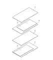
- FIG. 2 is an exploded perspective view showing a multilayer structure of an element body included in a multilayer ceramic capacitor as an example of a multilayer electronic component manufactured by the manufacturing method according to the present embodiment.
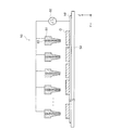
- FIG. 3 is a schematic cross-sectional view of an essential part of a discharge device used in the manufacturing method according to the present embodiment.
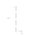
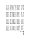
- FIG. 4A is a plan view for explaining a first step in the manufacturing method according to the present embodiment.
- FIG. 4B is a diagram following FIG. 4A.
- FIG. 4C is a diagram following FIG. 4B.
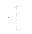
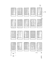
- FIG. 5A is a plan view for explaining a second step in the manufacturing method according to the present embodiment.
- FIG. 5B is a perspective view for explaining a second step in the manufacturing method according to the present embodiment.
- FIG. 6A is a diagram for explaining an overlapping portion of the green conductor portion.
- FIG. 6B is a diagram for explaining an overlapping portion of the green conductor portion.
- FIG. 7A shows that when the length of the conductor part and the position variation of the conductor part opposed to one conductor part follow a normal distribution, the capacitance of the functional part sandwiched between the two conductor parts is M It is a graph which shows the relationship with the ratio used as tolerance (+/- 20%).
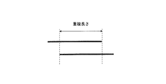
- FIG. 7B is a diagram showing the relationship of the conductor parts in the cross-section at the broken line in FIG. 6B.
- Multilayer electronic component Manufacturing method of multilayer electronic component 2.1. Discharge device 2.2. Ink 2.2.1. First ink 2.2.2. Second ink 2.2.3. Viscosity of resin solution 2.3. Manufacturing process 2.3.1. First step 2.3.2. Second step 2.3.3. Step of obtaining a green laminate 2.3.4. 2. obtaining an element body; Effect of the present embodiment 4. Modified example
- the multilayer ceramic capacitor 1 has an element main body 10, and as shown in FIGS. 1 and 2, the element main body 10 has a rectangular functional part (ceramic layer 2) and either the short side direction or the long side direction.
- the rectangular conductor portions (internal electrode layers 3) formed smaller than the functional portions are alternately laminated.
- a pair of terminal electrodes 4 are formed which are electrically connected to the internal electrode layers 3 arranged alternately in the element body 10.
- the ceramic layer disposed between the electrode layers showing different polarities exhibits a predetermined dielectric characteristic, and as a result, functions as a capacitor.
- the shape and dimensions of the multilayer electronic component may be appropriately determined according to the purpose and application, but in this embodiment, the case where the shape is a rectangular parallelepiped shape will be taken up.
- the dimensions are preferably small. In the case of a multilayer ceramic capacitor, the dimensions are, for example, vertical (0.4 mm or less) ⁇ horizontal (0.2 mm or less) ⁇ thickness (0.1 to 0.2 mm) or less. Is preferred.
- the ejection device 50 includes a plurality of nozzles 51 as ejection units and a voltage application unit 52, as shown in FIG.
- the ejection device includes at least a first head unit including a plurality of nozzles supplied with the first ink and a second head including a plurality of nozzles supplied with the second ink. And a head portion.
- the voltage application means 52 is connected to the nozzle 51 and the support 53 and can apply a voltage between the nozzle 51 and the support 53. Thereby, the ink 60 supplied into the nozzle from an ink supply unit (not shown) can be charged.
- the applied voltage is a high voltage of about several hundred volts to several thousand volts, and the same voltage can be applied to a plurality of nozzles electrically connected in parallel.
- the support 53 is held on a table 54 that can move in each of the X-axis, Y-axis, and Z-axis directions in response to an electrical signal from a control unit (not shown).
- the support 53 is also movable. If the nozzle and the drawing object can move relative to each other, the nozzle may move or the table may move.
- the voltage applying unit 52 applies a voltage corresponding to the electric signal to the nozzle 51.
- the control unit can also send an electrical signal to the table 54 to move the table 54 on the XY plane while keeping the distance between the nozzle 51 and the table 54 constant. Therefore, since the table moves on the XY plane in a state where the ink 60 is ejected onto the drawing object O, a pattern is drawn on the drawing object O.
- the voltage applying unit 52 sets the voltage applied to the nozzle 51 to zero.
- the ink 60 is separated from the drawing object O and pulled back to the nozzle 51 by the effect of the surface tension.
- the ink In the discharge device, the ink is charged, and the discharge start and discharge stop of the charged ink are controlled by electrostatic attraction force. Therefore, the ink discharge start and discharge stop are very fast and accurate with respect to voltage application. respond. Accordingly, when a voltage is applied, the ink is immediately ejected onto the object to be drawn, and when the voltage application is stopped, the ink ejection is immediately stopped without causing dripping or the like, so that a predetermined pattern can be repeatedly drawn with good reproducibility. .
- a voltage is applied so that the same pattern is simultaneously formed on the plurality of nozzles provided in the ejection device, that is, the voltage application pattern applied to the plurality of nozzles is the same. Therefore, only one power source may be used to apply a voltage to a plurality of nozzles mounted on one head, and it is necessary to configure the voltage application means so that different voltages are applied to the plurality of nozzles simultaneously to form different patterns. Absent. In addition, since the same voltage is applied to a plurality of nozzles forming the same pattern, there is no need for insulation treatment between adjacent nozzles. As a result, in the present embodiment, the configuration of the ejection device can be simplified.
- the first ink for forming the green functional part that constitutes the functional part and the green conductor part that constitutes the conductive part are used as the ink used in the above-described ejection device.
- a second ink for forming is prepared.
- the first ink and the second ink will be described.
- the first ink includes functional particles, a solvent, and a resin.
- the method for preparing the first ink is not particularly limited.
- a resin solution may be prepared by dissolving a resin in a solvent, and the resin solution and functional particles may be mixed.
- the functional particles are dispersed in the resin solution.
- the functional particle is not particularly limited as long as it is a material such as a material constituting the functional part or a compound serving as the material, and is appropriately selected according to the application.
- the material constituting the functional part is ceramic
- particles made of the ceramic, or particles of carbonate, nitrate, hydroxide, organometallic compound, etc. that become the ceramic by heat treatment or the like are exemplified. Is done.
- the material which comprises a functional part is a metal or an alloy
- grains comprised from the said metal or alloy are illustrated.
- the particle diameter of the functional particles may be determined in consideration of the heat treatment characteristics (sinterability, etc.) of the functional particles and the sedimentation of the functional particles dispersed in the first ink.
- the particle size is increased, the functional particles in the first ink are likely to settle, and the amount of ink discharged tends to vary during drawing.
- the line width of the drawn line, the thickness of the formed pattern, and the like are uniform. It tends to be unsustainable.
- the functional particles during the heat treatment of the green laminate tend to be sintered too quickly, and structural defects (cracks, delamination, etc.) due to simultaneous firing of the functional part and the conductor part. May occur, which is not preferable.
- the average particle diameter of the functional particles is preferably about 100 to 500 nm.
- an average particle diameter may be about several dozen nm in consideration of the influence of sedimentation of a functional particle.
- the resin contained in the first ink is not particularly limited, and examples thereof include cellulose resins, butyral resins, acrylic resins, polyvinyl alcohol, epoxy resins, phenol resins, styrene resins, and urethane resins.
- the solvent contained in the first ink is not particularly limited, and water or an organic solvent is exemplified.
- organic solvent examples include aliphatic hydrocarbons such as decane, tetradecane, and octadecane, ketones such as methyl ethyl ketone and cyclohexanone, aromatic hydrocarbons such as xylene and toluene, methyl cellosolve, butyl cellosolve, methyl carbitol, and butyl.
- Ethers such as carbitol and triethylene glycol monoethyl ether, esters such as ethyl acetate and butyl carbitol acetate, alcohols such as propanol, ethylene glycol and terpineol, polar such as dimethyl sulfoxide, N-methylpyrrolidone and dimethylacetamide Examples thereof include use of a single solvent or a mixture of a plurality of solvents.
- the first ink may contain a dispersant, a plasticizer, a dielectric, a glass frit, an insulator, a charge remover, and the like as necessary.
- the second ink includes conductive particles, a solvent, and a resin.
- the method for preparing the second ink is not particularly limited, but may be the same as the method for preparing the first ink.
- the conductor particles are not particularly limited as long as they are particles of a material constituting the conductor part or a compound serving as the material, and are appropriately selected according to compatibility with the material constituting the functional part, use, and the like.
- the particle diameter of the conductor particles is determined in consideration of the heat treatment characteristics (sinterability, etc.) of the conductor particles and the sedimentation of the conductor particles in the second ink, similarly to the particle diameter of the functional particles. That's fine.
- the average particle diameter of the conductor particles is preferably about 100 to 500 nm.
- an average particle diameter may be about several dozen nm in consideration of the influence of sedimentation of a functional particle.
- the ink has a viscosity as a resin solution that does not include particles (functional particles and conductor particles) of 30 mPa. -It is preferable that it is more than s.
- the particle diameter to be used can be as small as several tens of nm, sedimentation is suppressed even if the viscosity of the resin solution is small.
- the line width can be reduced, which is advantageous when an electronic component having an extremely small size is manufactured.
- the upper limit of the viscosity of the resin solution is not particularly limited as long as it can be ejected as ink and there is no problem in responsiveness.
- it is preferably 1200 mPa ⁇ s or less.
- the green function portion is formed by printing the green function portion with the first ink on the support or the green conductor portion (first step) using the above-described discharge device.
- a green conductor portion is printed and formed on the portion with the second ink (second step). Then, this process is repeated to obtain a green laminated body in which green functional portions and green conductor portions are alternately laminated, and then the green laminated body is processed to obtain an element body.
- each step will be described.
- the green function part is formed on the support.
- an electrostatic suction force is applied to the first ink
- Printing is performed by discharging the first ink onto the support.
- FIG. 4A when the application of the voltage is stopped at a predetermined time interval while the table (not shown) moves in the X-axis direction by a predetermined amount, the first drawn out while the voltage application is stopped. Ink discharge stops intermittently when one ink leaves the support and returns to the nozzle (not shown). As a result, a plurality of line segments L1 having a predetermined length parallel to the X-axis direction are formed on the support 53.
- a voltage is intermittently applied between the nozzle (not shown) and the support so as to be parallel to and in contact with the formed line segment L1, as shown in FIG. 4B.
- a line segment L2 is newly formed.
- a plurality of regions for example, rectangular regions (green function portion 12), in which a predetermined number of line segments are continuously formed are formed. If necessary, a rectangular green functional unit 12 having a desired thickness can be formed by repeatedly forming a line segment immediately above the formed rectangular region.
- the table is moved by a predetermined amount in the Y-axis direction so that the nozzle filled with the second ink is positioned on the green function portion formed in the first step.
- the table may be fixed, and the nozzle may be moved so that the nozzle filled with the second ink is positioned on the green function part formed in the first step.
- the second function is used to form a predetermined length on the green function portion, as in the first step.
- a line segment is formed, and by repeating this, a region in which a predetermined number of line segments having a predetermined length are formed, for example, a rectangular region (green conductor portion 13) is formed.
- the nozzle is not shown.
- FIG. 5B only the tip of the nozzle is shown.
- the conventional method when the length W1 in the short direction of the rectangular green conductor portion is 180 ⁇ m or less, the conventional method is effective in terms of product yield. In some cases, the yield improvement effect of the product becomes very large. According to the method according to this embodiment, since the formation accuracy of the internal structure of the multilayer electronic component is high, it can be formed with high accuracy even when the length of the green conductor portion in the short direction is extremely small. As a result, the yield of small electronic components can be increased.
- the reason why the length of the green conductor portion in the short direction is specified is that, for example, the influence of the length of the green conductor portion in the short direction on the electrostatic capacitance is the largest.
- the ratio of the length W1 in the short direction of the green conductor portion to the length W2 in the short direction of the green function portion should be increased. Is preferred. According to the method according to the present embodiment, since the formation accuracy of the green conductor portion can be increased, the length of the green conductor portion in the short direction can be increased, and the obtainable capacitance can be maximized. can do.
- the green conductor portion 13 is aligned with the green functional portion 12 so that the end portions thereof are at the same position, but the short direction (Y-axis direction). And about the longitudinal direction (X-axis direction), the green conductor part is formed smaller than the green function part. Therefore, after the green conductor portion is formed on the green function portion, there is a region (margin region 15) where nothing is formed on the green function portion.
- the thickness of the green functional portion When the thickness of the green functional portion is small, the thickness of the green conductor portion relative to the green functional portion is relatively large. Therefore, when the number of stacked layers in the multilayer electronic component is increased, the effect of the step between the green conductor portion and the blank area is affected. Occurs in the green laminate. As a result, structural defects (cracks, delamination, etc.) tend to occur easily during heat treatment of the green laminate. Therefore, the green functional part may be formed in the blank area 15 before and after forming the green conductor part. By doing so, the step between the green conductor portion and the blank area is eliminated, so that the occurrence of structural defects due to the step can be suppressed.
- the green function portion formed in the blank area may be formed using the first ink, or may be formed using an ink different from the first ink.
- the thickness of the green function part is large, the structure defect due to this tends to be small even if the green function part is not formed in the blank area. Therefore, the green function part is not formed in the blank area. Also good.
- the line width of the line segment formed using ink is about 5 to 50 ⁇ m.
- line segments having a predetermined length are repeatedly formed so as to be parallel and continuous, and a surface region having one thickness is formed by connecting the line segments in contact with each other.
- the line segment is formed by using the above-described discharge device that uses the electrostatic attraction force, a deviation (variation) in the length of the actually formed line segment from the length of the set line segment is detected. ) And the deviation (variation) of the actually formed position with respect to the set formation position can be made very small. Therefore, the deviation (variation) from the setting can be very small even for a rectangular region formed by connecting line segments. In other words, the formation accuracy of the rectangular region can be extremely increased.
- a line segment may be formed in parallel along the short or long direction of the rectangular region to be formed, and the rectangular region may be formed.
- a rectangular region may be formed by changing the length of a line segment formed in a diagonal direction of the region.
- the green function portion and the green conductor portion that determine the outer shape of the element are formed as a rectangle, but in the electronic component to be manufactured, the outer shape and the shape of the green conductor portion are Polygons such as hexagons and octagons may be used as basic shapes, and circles may be used as basic shapes.
- Step of obtaining a green laminate By repeating the first step and the second step, forming a green conductor portion on the green function portion and further forming a green function portion on the green conductor portion, A green laminate in which green conductor portions are alternately laminated is obtained.
- a green functional portion and a green conductor portion having a desired area are formed by forming a plurality of line segments in parallel and connected using an ejection device that uses electrostatic attraction force. ing.
- the thickness of the green functional part and the green conductor part suppresses unevenness of the in-plane thickness by adjusting the line width and the pitch width between the lines. Therefore, the length of the green functional part and the green conductor part in the short direction is at least twice the line width of the line segment.
- the green function part and the green conductor part are accurately formed and laminated using an ejection device that uses electrostatic attraction force, the formation accuracy of the resulting green laminate is very high. Therefore, when the green laminated body is viewed from the lamination direction, the area where the green conductor portions overlap can be made very large.
- the size of the region where the conductor portions overlap becomes a problem.
- the formation accuracy of the green conductor portions is low and the green conductor portions deviate from the ideal arrangement as shown in FIG. 6B.
- the overlap area OA of the green conductor portion is reduced by the amount of deviation.
- FIG. 7A shows a functional part sandwiched between two conductor parts when the length of the conductor part (electrode width) and the position variation of the conductor part facing one conductor part follow a normal distribution. It is a graph which shows the relationship with the ratio from which an electrostatic capacitance becomes general M tolerance (+/- 20%) as tolerance of the electrostatic capacitance of an electronic component.
- the diagram shown in FIG. 7B is a diagram showing the relationship of the conductor portions in the cross section at the broken line position in FIG. 6B.
- the length at which the two conductor portions shown in FIG. 7B overlap needs to be about 80% or more of the length of the line segment. .
- the vertical axis in FIG. 7A indicates the ratio of those with a small displacement of the opposing conductor portions (overlapping length is about 80% or more).
- the deviation from the set formation position depends on the formation accuracy as described above. Therefore, if the formation accuracy is high, the distribution of deviation from the set formation position when a predetermined number of line segments are formed is small. Conversely, if the formation accuracy is low, the distribution of deviation is large.
- the standard deviation ⁇ of the deviation distribution can be realized to 3 ⁇ m or less in the method according to the present embodiment, whereas the conventional screen printing or the like It was found that the standard deviation ⁇ of the deviation distribution was about 15 ⁇ m.
- FIG. 7A shows the result of calculating the relationship between the length of the line segment to be formed and the ratio within the M tolerance using the value of the standard deviation ⁇ .
- the ratio within the M tolerance is almost 100% even when the length of the line segment is about 30 ⁇ m. Then, when the length of the line segment becomes smaller than about 180 ⁇ m, the ratio within the M tolerance is clearly less than 100%.
- FIG. 7A shows the yield prediction in the line segment, that is, in one axis direction.
- the green conductor portion is formed in a rectangular shape (biaxial direction), and further, lamination deviation occurs in the lamination direction (height direction) due to the lamination. Therefore, regarding the multilayer electronic component, it is certain that the yield difference between the method according to this embodiment and the conventional method is larger than the difference shown in FIG. 7A.
- the obtained green laminate is processed to obtain an element body.
- heat treatment is exemplified.
- the heat treatment include a binder removal process, a baking process, and an annealing process.
- the functional particles included in the green functional part are integrated into a functional part
- the conductive particles included in the green conductive part are integrated into a conductive part.
- the green laminate is formed as a green chip corresponding to the shape and dimensions of the element body, the element body can be obtained by heat treatment as it is without cutting the green laminate. Since the green chip contracts during heat treatment to become an element body, the size of the green chip is larger than the dimension of the element body.
- the green laminate formed to have a size larger than that of the green chip may be cut and separated into pieces to obtain a plurality of green chips. Moreover, you may perform a well-known process with respect to a green laminated body other than the process mentioned above.
- an element body having a configuration in which the functional part and the conductor part are laminated can be obtained.
- a terminal-type electrode etc. can be formed with respect to the obtained element main body as needed, and a multilayer electronic component can be obtained.
- the formation accuracy of the line segment formed using the discharge device using electrostatic attraction force is very high, and a rectangular region formed by connecting a plurality of these can be formed with high accuracy. Further, since the length of the rectangular region in the short direction is twice or more the width of the line segment to be formed, the variation in the thickness direction of the printed region can be very small.
- the formation accuracy of the green functional part and the green conductor part can be increased in both the planar direction and the lamination direction under a specific problem of increasing the formation accuracy of the laminate.
- a multilayer electronic component with improved internal structure formation accuracy can be obtained.
- the length in the hand direction is 180 ⁇ m or less, it is possible to dramatically improve the ratio (yield) of products whose capacitance is within the M tolerance as compared with the conventional method.
- the same voltage is simultaneously applied to the plurality of nozzles provided in the discharge device, the same shape can be formed simultaneously by the number of nozzles.
- the discharge device having such a configuration even if a plurality of nozzles are provided, there is only one voltage applying means for applying a voltage to the nozzles, and the same voltage is simultaneously applied to the plurality of nozzles. Insulation is not necessary. Therefore, when the discharge device is used in the manufacturing method according to the present embodiment, the disadvantages of the discharge device can be used as an advantage.
- the step of cutting and dividing the green laminated body into a plurality of green chips can be omitted.
- disconnection of a green laminated body can be suppressed.
- the particles are used in the ink.
- the viscosity of the resin solution not included in the above-described range, it is possible to obtain an ink in which sedimentation of particles is effectively suppressed.
- the particle concentration and viscosity of the ink are stabilized, and the uniformity of the width of the line segment is improved, thereby improving the uniformity of the thickness of the functional part and the conductor part.
- a multilayer electronic component with high formation accuracy can be obtained.
- the multilayer ceramic capacitor is exemplified as the multilayer electronic component, but various multilayer electronic components are exemplified according to the material constituting the functional layer.
- a multilayer varistor, a multilayer thermistor, a multilayer piezoelectric element, a multilayer inductor, etc. are illustrated.
- the functional layer is composed of a semiconductor ceramic layer.
- the functional layer is composed of a piezoelectric ceramic layer.
- the layer is composed of a ferrite layer or a soft magnetic metal layer.
- the material which comprises a conductor part is determined according to the material of a function part.
- each green functional portion and each green conductor portion are the same.
- the coil conductor is rectangular.
- a helical conductor may be formed.
- a green laminated body of a laminated composite electronic component it is formed by using two or more types of functional particle material constituting the green functional part and conductive particle material constituting the green conductive part. May be.
- a first ink and a second ink were prepared.
- the first ink 5 parts by weight of a butyral resin as a resin and butyl cellosolve as a solvent are mixed to prepare a resin solution, and barium titanate particles as functional particles are dispersed in the resin solution. Produced.
- the viscosity of the resin solution was 50 mPa ⁇ s.
- the average particle diameter of the barium titanate particles was 200 nm.
- the second ink was prepared by mixing a butyral resin as a resin and butyl cellosolve as a solvent to prepare a resin solution, and dispersing nickel particles as conductor particles in the resin solution.
- the viscosity of the resin solution was 46 mPa ⁇ s.
- the average particle diameter of the nickel particles was 100 nm.
- a dielectric layer as a green functional part and a green conductor part
- the internal electrode layers were alternately formed to form a green laminate having 75 internal electrodes.
- the dimensions of the dielectric layer were 220 ⁇ m in the short direction and 460 ⁇ m in the long direction. Moreover, the dimension of the internal electrode layer was 140 ⁇ m in the short direction.
- the obtained green chip was subjected to binder removal treatment in an air atmosphere at 250 ° C. for 10 hours, and then fired in a reducing atmosphere at 1200 ° C. for 1 hour to obtain an element body.
- a terminal electrode was formed on the obtained element body to obtain a multilayer ceramic capacitor sample.
- the size of the element after sintering was about 0.4 mm ⁇ about 0.2 mm ⁇ about 0.2 mm.
- Example 2 Resin solutions having different viscosities were prepared by changing the amount of butyral resin as the resin and the amount of butyl cellosolve as the solvent. Table 1 shows the viscosity of the resin solution. Furthermore, ceramic particles having a density of 6 g / cm 3 and an average particle size of 300 nm were dispersed in these resin solutions to prepare inks. The viscosity of the ink is shown in Table 1.
- Each of the produced inks was filled into the nozzle of the ejection device used in Experimental Example 1, and the ink was ejected to form a 10 mm line segment.
- the line width was measured every 1 mm, and the average line width and the standard deviation of the line width were calculated. Further, the CV value was calculated from the calculated standard deviation ⁇ . The results are shown in Table 1.
Landscapes
- Engineering & Computer Science (AREA)
- Power Engineering (AREA)
- Manufacturing & Machinery (AREA)
- Microelectronics & Electronic Packaging (AREA)
- Chemical & Material Sciences (AREA)
- Ceramic Engineering (AREA)
- Inorganic Chemistry (AREA)
- Fixed Capacitors And Capacitor Manufacturing Machines (AREA)
- Ceramic Capacitors (AREA)
- Manufacturing Cores, Coils, And Magnets (AREA)
Abstract
【課題】機能部と導電体部とが積層されて形成される積層体の形成精度が極めて良好な積層型電子部品の製造方法を提供すること。 【解決手段】機能部と導電体部とが積層された素子本体を有する積層型電子部品の製造方法であって、電圧印加手段により吐出部内のインクを帯電させ、帯電したインクを静電吸引力により吐出部から吐出する吐出装置を用いて、インクとして、機能性粒子を含む第1のインクを用いて、グリーン機能部12を形成する第1の工程と、インクとして、導電体粒子を含む第2のインクを用いて、グリーン導電体部13を形成する第2の工程と、第1の工程と第2の工程とを繰り返して、グリーン積層体を形成する工程と、グリーン積層体を処理して素子本体を得る工程と、を有する、積層型電子部品の製造方法である。
Description
本発明は、積層型電子部品の製造方法に関する。
電子機器には、情報処理、信号変換等のため、あるいは電源回路等に、多数かつ種々の電子部品が搭載されている。このような電子部品として、当該電子部品の性能を発揮する機能層と、端子に電気的に接続される電極層とが積層された構成を有する積層型電子部品が知られている。
従来、積層型電子部品を製造する方法としては、たとえば、プラスチックフィルム上に印刷技術を利用して所定のパターンを形成して素子を得るロールtoロールと呼ばれる工程を利用する方法が例示される。
具体的には、プラスチックフィルム上に、機能層を構成する材料を含むスラリーを用いてシートを形成し、その上に電極層を構成する導電体材料を含むペーストを用いて電極を印刷する。続いて、電極が形成されたシートを積層して、シートと電極とが積層された成形体を得る。そして、得られた成形体を必要に応じて切断して、個片化した後、熱処理することにより、積層型電子部品が製造される。
しかしながら、上記のような方法では、積層時および切断時に電極の位置ずれが生じやすく、得られる積層型電子部品における機能層と電極層との積層構造の形成精度が低下する要因となっていた。
形成精度を高める方法として、たとえば、特許文献1には、セラミックスラリーと、導電体材料を含む機能材料ペーストとをインクジェット方式により液滴を噴射して、セラミック層と電極層とを形成して、積層型電子部品を製造する方法が記載されている。この方法によれば、位置ずれを抑制でき、かつ積層工程および切断工程を不要とすることができると記載されている。
また、特許文献2には、インクジェット方式を利用した液滴の噴射による積層型電子部品の製造に適したインクが記載されている。
本発明は、このような実状に鑑みてなされ、その目的は、機能部と導電体部とが積層されて形成される積層体の形成精度が極めて良好な積層型電子部品の製造方法を提供することである。
近年、電子機器の高性能化、小型化等の要求により、電子部品についても、高性能化、小型化等が求められている。電子部品の小型化を進めると、製造された電子部品が所定の規格(性能)を満足する割合(歩留まり)が急激に低下してしまう。これは電子部品の小型化に伴って積層体の形成精度が低下し、電子部品の特性(性能)に大きな影響を与え、所定の最大公差内となる特性を有する電子部品の数が少なくなってしまうことに起因している。そこで、本発明者らは、積層体の形成精度をさらに高めるべく種々の検討を行った。
その結果、従来のロールtoロール工法では、形成精度の向上には限界があり、特にサイズの小さい積層型電子部品の特性(たとえば、積層セラミックコンデンサにおける静電容量、NTCサーミスタにおける電気抵抗等)を所定の規格内に収めることが困難であり、その結果、歩留まりが低下することを見出した。また特許文献1には詳細が記載されていないが、通常のインクジェット方式により液滴を噴射する場合でも着弾精度は10μm程度しかないために、従来のロールtoロールの工法と比べて格段の形成精度の向上は見込めず、十分ではなかった。
本発明の態様は、
[1]機能部と導電体部とが積層された素子本体を有する積層型電子部品の製造方法であって、
電圧印加手段により吐出部内のインクを帯電させ、帯電したインクを静電吸引力により吐出部から吐出する吐出装置を用いて、
インクとして、機能性粒子を含む第1のインクを用いて、グリーン機能部を形成する第1の工程と、
インクとして、導電体粒子を含む第2のインクを用いて、グリーン導電体部を形成する第2の工程と、
第1の工程と第2の工程とを繰り返して、グリーン積層体を形成する工程と、
グリーン積層体を処理して素子本体を得る工程と、を有する積層型電子部品の製造方法である。
[1]機能部と導電体部とが積層された素子本体を有する積層型電子部品の製造方法であって、
電圧印加手段により吐出部内のインクを帯電させ、帯電したインクを静電吸引力により吐出部から吐出する吐出装置を用いて、
インクとして、機能性粒子を含む第1のインクを用いて、グリーン機能部を形成する第1の工程と、
インクとして、導電体粒子を含む第2のインクを用いて、グリーン導電体部を形成する第2の工程と、
第1の工程と第2の工程とを繰り返して、グリーン積層体を形成する工程と、
グリーン積層体を処理して素子本体を得る工程と、を有する積層型電子部品の製造方法である。
上記の製造方法では、静電吸引力を利用した吐出装置を用いて、グリーン機能部およびグリーン導電体部を直接印刷し、これら重ね印刷を繰り返してグリーン積層体を得ている。静電吸引力を利用した吐出装置を用いることで、ノズルとワークとの間隔を100μm以下としても安定して吐出することが出来るため、高い精度で印刷を行うことが出来る。このようなグリーン積層体によれば、形成精度が非常に高い積層型電子部品を得ることができる。
[2]グリーン積層体は、素子本体の形状および寸法に対応しているグリーンチップである[1]に記載の積層型電子部品の製造方法である。
上記の製造方法では、グリーンチップが最初から個片化されたグリーン積層体として形成されるので、グリーン積層体を切断して個片化された複数のグリーンチップとする工程を省略することができる。その結果、積層型電子部品の特性または電気抵抗等の変動を抑制することができる。
[3]グリーン導電体部が矩形状であり、その短手方向の幅が180μm以下である[1]または[2]に記載の積層型電子部品の製造方法である。
上記の製造方法は、積層型電子部品の内部構造の形成精度を高めることができるので、寸法が非常に小さい小型の積層型電子部品の製造方法として好適である。
[4]インクは溶媒と樹脂とを含み、当該溶媒と当該樹脂とからなる溶液の粘度が30mPa・s以上である[1]から[3]のいずれかに記載の積層型電子部品の製造方法である。
溶液の粘度を上記の範囲内とすることにより、インクが吐出されて形成される線分の線幅の均一性および印刷した領域の厚みの均一性を確保することができる。
[5]吐出装置において、複数のノズルに同一の電圧が同時に印加される[1]から[4]のいずれかに記載の積層型電子部品の製造方法である。
吐出装置が上記の構成を有していることにより、複数のグリーン積層体を同時に形成することができる。
以下、本発明を、図面に示す実施形態に基づき、以下の順序で詳細に説明する。
1.積層型電子部品
2.積層型電子部品の製造方法
2.1. 吐出装置
2.2. インク
2.2.1. 第1のインク
2.2.2. 第2のインク
2.2.3. 樹脂溶液の粘度
2.3. 製造工程
2.3.1. 第1の工程
2.3.2. 第2の工程
2.3.3. グリーン積層体を得る工程
2.3.4. 素子本体を得る工程
3.本実施形態の効果
4.変形例
1.積層型電子部品
2.積層型電子部品の製造方法
2.1. 吐出装置
2.2. インク
2.2.1. 第1のインク
2.2.2. 第2のインク
2.2.3. 樹脂溶液の粘度
2.3. 製造工程
2.3.1. 第1の工程
2.3.2. 第2の工程
2.3.3. グリーン積層体を得る工程
2.3.4. 素子本体を得る工程
3.本実施形態の効果
4.変形例
(1.積層型電子部品)
本実施形態に係る製造方法により製造される積層型電子部品の一例として、積層セラミックコンデンサを図1に示す。積層セラミックコンデンサ1は、素子本体10を有しており、図1および図2に示すように、素子本体10は、矩形状の機能部(セラミック層2)と、短手方向および長手方向のどちらにおいても機能部よりも小さく形成された矩形状の導電体部(内部電極層3)と、が交互に積層されて構成されている。素子本体10の両端部には、素子本体10の内部で交互に配置された内部電極層3と各々導通する一対の端子電極4が形成してある。
本実施形態に係る製造方法により製造される積層型電子部品の一例として、積層セラミックコンデンサを図1に示す。積層セラミックコンデンサ1は、素子本体10を有しており、図1および図2に示すように、素子本体10は、矩形状の機能部(セラミック層2)と、短手方向および長手方向のどちらにおいても機能部よりも小さく形成された矩形状の導電体部(内部電極層3)と、が交互に積層されて構成されている。素子本体10の両端部には、素子本体10の内部で交互に配置された内部電極層3と各々導通する一対の端子電極4が形成してある。
この端子電極に電圧を印加することにより、異なる極性を示す電極層間に配置されているセラミック層が所定の誘電特性を発揮し、その結果コンデンサとして機能する。
積層型電子部品の形状および寸法は、目的および用途に応じて適宜決定すればよいが、本実施形態では、形状は直方体形状である場合について取り上げる。また、寸法は小さいことが好ましく、積層セラミックコンデンサの場合、その寸法は、例えば縦(0.4mm以下)×横(0.2mm以下)×厚み(0.1~0.2mm)以下であることが好ましい。
(2.積層型電子部品の製造方法)
続いて、本実施形態に係る製造方法の一例について下記に詳細に説明する。本実施形態に係る製造方法では、静電吸引力を利用した吐出装置を用いて、機能部となるグリーン機能部と、導電体部となるグリーン導電体部とを印刷形成する。まず、本実施形態に係る製造方法において用いられる吐出装置について説明する。
続いて、本実施形態に係る製造方法の一例について下記に詳細に説明する。本実施形態に係る製造方法では、静電吸引力を利用した吐出装置を用いて、機能部となるグリーン機能部と、導電体部となるグリーン導電体部とを印刷形成する。まず、本実施形態に係る製造方法において用いられる吐出装置について説明する。
(2.1. 吐出装置)
本実施形態では、吐出装置50は、図3に示すように、吐出部としての複数のノズル51と、電圧印加手段52とを備えている。図3では明示していないが、吐出装置は少なくとも、第1のインクが供給された複数のノズルを備える第1のヘッド部と、第2のインクが供給された複数のノズルを備える第2のヘッド部とから構成されている。
本実施形態では、吐出装置50は、図3に示すように、吐出部としての複数のノズル51と、電圧印加手段52とを備えている。図3では明示していないが、吐出装置は少なくとも、第1のインクが供給された複数のノズルを備える第1のヘッド部と、第2のインクが供給された複数のノズルを備える第2のヘッド部とから構成されている。
電圧印加手段52は、ノズル51と支持体53とに接続されており、ノズル51と支持体53との間に電圧を印加することができる。これにより、図示しないインク供給部からノズル内に供給されたインク60を帯電させることができる。なお、印加される電圧は数100Vから数1000V程度の高電圧であり、並列に電気的に接続された複数のノズルに同一の電圧を印加することができる。
また、支持体53は、図示しない制御部からの電気信号に応じてX軸、Y軸、Z軸の各方向に移動可能なテーブル54上に保持されており、テーブル54の移動に対応して支持体53も移動可能とされる。なお、ノズルと描画対象物とが相対的に移動できれば、ノズルが移動してもよいし、テーブルが移動してもよい。
吐出装置50において、図示しない制御部が電気信号を電圧印加手段52に送ると、電圧印加手段52が当該電気信号に対応した電圧をノズル51に印加する。このような制御を行うことにより、帯電したインク60がノズル51から静電吸引力により引き出され、描画対象物O(支持体、または、支持体上に形成されたグリーン機能部またはグリーン導電体部)に吐出される。このとき、制御部は、テーブル54にも電気信号を送り、ノズル51とテーブル54との距離を一定に維持しながらテーブル54をXY平面上で移動させることができる。したがって、インク60が描画対象物Oに吐出された状態でテーブルがXY平面上を移動するので、描画対象物Oにパターンが描画される。
制御部が電気信号の送信を停止すると、電圧印加手段52はノズル51に印加する電圧を0とする。その結果、インク60に静電吸引力が作用しなくなるので、インク60は表面張力の効果により描画対象物Oから離れノズル51に引き戻される。この一連の動作により、描画対象物に対し所定のパターンを形成することができる。
吐出装置では、インクを帯電させ、帯電したインクの吐出開始および吐出停止を静電吸引力により制御しているため、電圧印加に対して、インクの吐出開始および吐出停止が非常に速くかつ精度よく応答する。したがって、電圧を印加すると、直ちにインクが描画対象物に吐出され、電圧印加を停止すると、液だれ等を生じることなく、直ちにインクの吐出が停止するので、所定のパターンを繰り返し再現性よく描画できる。
本実施形態では、吐出装置が備える複数のノズルには同一のパターンを同時に形成するように電圧が印加される、すなわち、複数のノズルに印加される電圧の印加パターンは同じである。したがって、1つのヘッドに実装した複数のノズルに電圧を印加する電源は1つでよく、複数のノズルに同時に異なる電圧を印加して同時に異なるパターンを形成するように電圧印加手段を構成する必要はない。また、同一パターンを形成する複数のノズルには同じ電圧が印加されているため、近接しているノズル間の絶縁処理は必要ない。その結果、本実施形態では、吐出装置の構成を簡易な構成にすることができる。
(2.2. インク)
本実施形態では、上記の吐出装置で用いるインクとして、機能部を構成することとなるグリーン機能部を形成するための第1のインクと、導電体部を構成することとなるグリーン導電体部を形成するための第2のインクとを準備する。以下、第1のインクおよび第2のインクについて説明する。
本実施形態では、上記の吐出装置で用いるインクとして、機能部を構成することとなるグリーン機能部を形成するための第1のインクと、導電体部を構成することとなるグリーン導電体部を形成するための第2のインクとを準備する。以下、第1のインクおよび第2のインクについて説明する。
(2.2.1. 第1のインク)
本実施形態では、第1のインクは機能性粒子と溶媒と樹脂とを含む。第1のインクを調製する方法は特に制限されないが、たとえば、樹脂を溶媒に溶解して樹脂溶液を作製し、この樹脂溶液と機能性粒子とを混合すればよい。第1のインクにおいて、機能性粒子は樹脂溶液中に分散している。
本実施形態では、第1のインクは機能性粒子と溶媒と樹脂とを含む。第1のインクを調製する方法は特に制限されないが、たとえば、樹脂を溶媒に溶解して樹脂溶液を作製し、この樹脂溶液と機能性粒子とを混合すればよい。第1のインクにおいて、機能性粒子は樹脂溶液中に分散している。
機能性粒子としては、機能部を構成する材料または当該材料となる化合物等の粒子であれば、特に制限されず、用途等に応じて適宜選択される。たとえば、機能部を構成する材料がセラミックである場合には、当該セラミックから構成される粒子、または、熱処理等により当該セラミックとなる炭酸塩、硝酸塩、水酸化物、有機金属化合物等の粒子が例示される。また、たとえば、機能部を構成する材料が金属または合金である場合には、当該金属または合金から構成される粒子が例示される。
機能性粒子の粒子径は、機能性粒子の熱処理特性(焼結性等)と、第1のインク中に分散している機能性粒子の沈降と、を考慮して決定すればよい。粒子径が大きくなると、第1のインクにおいて機能性粒子の沈降が生じやすく、描画時にインクの吐出量がばらつく傾向にあり、描画した線分の線幅、形成したパターンの厚み等の均一性が維持できない傾向にある。また、粒子径が小さくなると、グリーン積層体の熱処理時における機能性粒子の焼結が速すぎる傾向にあり、機能部と導電体部との同時焼成に起因する構造欠陥(クラックやデラミネーション等)が発生する可能性があり、好ましくない。本実施形態では、機能性粒子の熱処理特性の観点から、機能性粒子の平均粒子径は100~500nm程度であることが好ましい。なお、熱処理に係る制限がない場合には、機能性粒子の沈降の影響を考慮して、平均粒子径は数十nm程度であってもよい。
第1のインクに含まれる樹脂は、特に制限されず、セルロース系樹脂、ブチラール系樹脂、アクリル系樹脂、ポリビニルアルコール、エポキシ樹脂、フェノール樹脂、スチレン樹脂、ウレタン樹脂等の樹脂が例示される。また、第1のインクに含まれる溶媒も特に制限されず、水または有機溶剤が例示される。具体的な有機溶剤としては、デカン、テトラデカン、オクタデカン等の脂肪族炭化水素類、メチルエチルケトン、シクロヘキサノン等のケトン類、キシレン、トルエン等の芳香族炭化水素類、メチルセロソルブ、ブチルセロソルブ、メチルカルビトール、ブチルカルビトール、トリエチレングリコールモノエチルエーテル等のエーテル類、酢酸エチル、ブチルカルビトールアセテート等のエステル類、プロパノール、エチレングリコール、テルピネオール等のアルコール類、ジメチルスルホキシド、N-メチルピロリドン、ジメチルアセトアミド等の極性溶媒等を単独、または複数混合して用いる等が例示される。
なお、第1のインクは、必要に応じて、分散剤、可塑剤、誘電体、ガラスフリット、絶縁体、帯電除剤等を含んでもよい。
(2.2.2. 第2のインク)
本実施形態では、第2のインクは導電体粒子と溶媒と樹脂とを含む。第2のインクを調製する方法は特に制限されないが、第1のインクを調製する方法と同様にすればよい。
本実施形態では、第2のインクは導電体粒子と溶媒と樹脂とを含む。第2のインクを調製する方法は特に制限されないが、第1のインクを調製する方法と同様にすればよい。
導電体粒子としては、導電体部を構成する材料または当該材料となる化合物等の粒子であれば特に制限されず、機能部を構成する材料との相性、用途等に応じて適宜選択される。
導電体粒子の粒子径は、機能性粒子の粒子径と同様に、導電体粒子の熱処理特性(焼結性等)と、第2のインクにおける導電体粒子の沈降と、を考慮して決定すればよい。本実施形態では、導電体粒子の熱処理特性の観点から、導電体粒子の平均粒子径は100~500nm程度であることが好ましい。なお、熱処理に係る制限がない場合には、機能性粒子の沈降の影響を考慮して、平均粒子径は数十nm程度であってもよい。
(2.2.3. 樹脂溶液の粘度)
本実施形態では、粒子(機能性粒子および導電体粒子)の沈降と、描画される線分の線幅とを考慮して、インクにおける粒子(機能性粒子および導電体粒子)を含まない樹脂溶液の粘度を決定することが好ましい。上述したように、インクにおいて粒子の沈降が生じると、描画時にインクの吐出量がばらつく傾向にあり、描画した線分の線幅の均一性、形成したパターンの厚みの均一性等が維持できない傾向にある。
本実施形態では、粒子(機能性粒子および導電体粒子)の沈降と、描画される線分の線幅とを考慮して、インクにおける粒子(機能性粒子および導電体粒子)を含まない樹脂溶液の粘度を決定することが好ましい。上述したように、インクにおいて粒子の沈降が生じると、描画時にインクの吐出量がばらつく傾向にあり、描画した線分の線幅の均一性、形成したパターンの厚みの均一性等が維持できない傾向にある。
ここで、慣性力と粘性力との比で表される無次元数Re数(=ρw・v・a/μ)が2未満の場合に、ストークスの法則を適用することができることを考慮して、粒子の沈降速度にストークスの法則を適用する。このストークスの法則によれば、平衡沈降速度vは、溶液の粘度μと粒子径a、溶液の密度ρwと粒子の密度ρsから、v=(ρs-ρw)g・a2/18μで示される。この式から分かるように沈降時の平衡速度は溶液の粘度に反比例する。したがって、インクに含まれる粒子が沈降することによりインク内の粒子密度が偏ることを抑制するためには、粒子を含むインクの粘度ではなく、インクに含まれる粒子を除いた溶液、すなわち、樹脂溶液の粘度を大きくすることが有効である。
本実施形態では、描画した線分の線幅、形成したパターンの厚み等の均一性の観点から、インクにおいて、粒子(機能性粒子および導電体粒子)を含まない樹脂溶液としての粘度が、30mPa・s以上であることが好ましい。
なお、本発明者らが検討した結果、樹脂溶液中の樹脂濃度と樹脂溶液の粘度との関係と、インク中の樹脂濃度とインクの粘度との関係と、を比較すると、どちらの場合であっても、樹脂濃度と粘度の常用対数とが比例関係にあるが、インクの粘度は、粒子の濃度、粒子径等により変化する傾向にあることが判明した。このことは、粒子の沈降を抑制するための粘度を規定する場合、インクの粘度ではなく、樹脂溶液の粘度の方が好ましいことを示している。
一方、使用する粒子径を数10nmと小さく出来る場合には、樹脂溶液の粘度が小さくても沈降が抑制される。このような樹脂溶液の粘度が小さい場合には線幅を小さく出来るため、寸法が極めて小さい電子部品を製造する場合に有利となる。
また、樹脂溶液の粘度の上限は、インクとして吐出可能であり応答性に問題がなければ特に制限されず、たとえば、1200mPa・s以下であることが好ましい。
(2.3. 製造工程)
本実施形態に係る製造方法では、上記の吐出装置を用いて、支持体上またはグリーン導電体部上に第1のインクによりグリーン機能部を印刷形成し(第1の工程)、形成したグリーン機能部の上に第2のインクによりグリーン導電体部を印刷形成する(第2の工程)。そして、これを繰り返して、グリーン機能部とグリーン導電体部とが交互に積層されたグリーン積層体を得てから、グリーン積層体を処理して素子本体を得る。以下、各工程について説明する。
本実施形態に係る製造方法では、上記の吐出装置を用いて、支持体上またはグリーン導電体部上に第1のインクによりグリーン機能部を印刷形成し(第1の工程)、形成したグリーン機能部の上に第2のインクによりグリーン導電体部を印刷形成する(第2の工程)。そして、これを繰り返して、グリーン機能部とグリーン導電体部とが交互に積層されたグリーン積層体を得てから、グリーン積層体を処理して素子本体を得る。以下、各工程について説明する。
(2.3.1. 第1の工程)
本実施形態では、グリーン機能部が支持体上に形成される。本工程では、図3に示すように、吐出装置において、第1のインクが供給された複数のノズルに印加する電圧を制御することにより、第1のインクに静電吸引力を作用させて、支持体上に第1のインクを吐出して印刷する。図4Aに示すように、テーブル(図示省略)が所定量だけX軸方向に移動しながら、所定の時間間隔で電圧の印加を停止すると、電圧の印加が停止している間、引き出された第1のインクが支持体上から離れてノズル(図示省略)に戻ることによりインクの吐出が断続的に停止する。その結果、支持体53上にX軸方向に平行な所定の長さの線分L1が複数形成される。
本実施形態では、グリーン機能部が支持体上に形成される。本工程では、図3に示すように、吐出装置において、第1のインクが供給された複数のノズルに印加する電圧を制御することにより、第1のインクに静電吸引力を作用させて、支持体上に第1のインクを吐出して印刷する。図4Aに示すように、テーブル(図示省略)が所定量だけX軸方向に移動しながら、所定の時間間隔で電圧の印加を停止すると、電圧の印加が停止している間、引き出された第1のインクが支持体上から離れてノズル(図示省略)に戻ることによりインクの吐出が断続的に停止する。その結果、支持体53上にX軸方向に平行な所定の長さの線分L1が複数形成される。
続いて、テーブル(図示省略)がY軸方向に所定量移動した後、再びテーブルがX軸方向に移動する。線分L1の形成時と同様に、ノズル(図示省略)と支持体との間に電圧が断続的に印加され、図4Bに示すように、形成された線分L1と平行かつ接触するように線分L2が新たに形成される。これを所定の回数繰り返すことにより、図4Cに示すように、所定の長さの線分が所定数連なって形成される領域、例えば矩形状の領域(グリーン機能部12)が複数形成される。必要に応じて、形成された矩形状の領域の直上に、さらに線分が連なるように繰り返し形成することにより、所望の厚みを有する矩形状のグリーン機能部12を形成することができる。
(2.3.2. 第2の工程)
第2の工程では、第2のインクが充填されたノズルが第1の工程において形成されたグリーン機能部の上に位置するように、テーブルがY軸方向に所定量移動する。あるいは、テーブルを固定し、第2のインクが充填されたノズルが第1の工程において形成されたグリーン機能部の上に位置するようにノズルが移動してもよい。
第2の工程では、第2のインクが充填されたノズルが第1の工程において形成されたグリーン機能部の上に位置するように、テーブルがY軸方向に所定量移動する。あるいは、テーブルを固定し、第2のインクが充填されたノズルが第1の工程において形成されたグリーン機能部の上に位置するようにノズルが移動してもよい。
第1の工程において形成したグリーン機能部が乾燥した後、図5Aおよび5Bに示すように、第1の工程と同様に、グリーン機能部上に、第2のインクを用いて所定の長さの線分が形成され、これを繰り返すことにより、所定の長さの線分が所定数連なって形成される領域、例えば矩形状の領域(グリーン導電体部13)が形成される。なお、図5Aではノズルの図示は省略してある。また、図5Bでは、ノズルに関して、その先端部のみを図示している。
本実施形態では、矩形状のグリーン導電体部の短手方向の長さW1は、180μm以下である場合に従来の工法に対して製品の歩留まり面で効果を発揮するが、ことに60μm以下である場合に製品の歩留まりの改善効果が非常に大きくなる。本実施形態に係る方法によれば、積層型電子部品の内部構造の形成精度が高いため、グリーン導電体部の短手方向の長さが極めて小さい場合であっても精度よく形成できる。その結果、小型の電子部品の歩留まりを高めることができる。グリーン導電体部の短手方向の長さについて規定するのは、例えば静電容量に対してグリーン導電体部の短手方向の長さの影響が最も大きいからである。
また、特に、積層セラミックコンデンサの場合、高い誘電特性を発揮するためには、グリーン機能部の短手方向の長さW2に対するグリーン導電体部の短手方向の長さW1の割合を大きくすることが好ましい。本実施形態に係る方法によれば、グリーン導電体部の形成精度を高めることができるので、グリーン導電体部の短手方向の長さを大きくすることができ、取得できる静電容量を極大化することができる。
なお、図5Aおよび5Bに示すように、グリーン機能部12に対して、グリーン導電体部13は、その端部が同じ位置となるように揃えられているが、短手方向(Y軸方向)および長手方向(X軸方向)については、グリーン導電体部は、グリーン機能部よりも小さく形成されている。したがって、グリーン機能部上にグリーン導電体部が形成された後には、グリーン機能部上に何も形成されていない領域(余白領域15)が存在する。
グリーン機能部の厚みが薄い場合、グリーン機能部に対するグリーン導電体部の厚みが相対的に大きくなるので、積層型電子部品における積層数が多くなると、グリーン導電体部と余白領域との段差の影響がグリーン積層体に生じる。その結果、グリーン積層体の熱処理時等において構造欠陥(クラックやデラミネーション等)が発生しやすい傾向にある。そのため、グリーン導電体部を形成する前後に、余白領域15にグリーン機能部を形成してもよい。このようにすることにより、グリーン導電体部と余白領域との段差が解消されるので、当該段差に起因する構造欠陥の発生を抑制することができる。
また、余白領域に形成されるグリーン機能部は第1のインクを用いて形成してもよいし、第1のインクとは異なるインクを用いて形成してもよい。
なお、グリーン機能部の厚みが大きい場合には、余白領域にグリーン機能部を形成しなくても、これに起因する構造欠陥は少ない傾向にあるので、余白領域にグリーン機能部を形成しなくてもよい。
本実施形態では、第1の工程および第2の工程において、インクを用いて形成される線分の線幅は5から50μm程度である。本実施形態では、所定の長さの線分を平行かつ連なるように繰り返し形成し、線分を互いに接触させて連結した1つの厚みをもった面領域を形成する。
本実施形態では、上述した静電吸引力を利用する吐出装置を用いて線分を形成しているため、設定した線分の長さに対する実際に形成された線分の長さのずれ(バラツキ)、および、設定した形成位置に対する実際に形成された位置のずれ(バラツキ)を非常に小さくすることができる。したがって、線分が連結されて形成される矩形の領域についても設定からのずれ(バラツキ)を非常に小さくすることができる。換言すれば、矩形の領域の形成精度を非常に高くすることができる。
矩形状の領域の形成方法としては、形成される矩形状の領域の短手方向または長手方向に沿って線分を平行に形成し、矩形状の領域としてもよいし、線分を矩形状の領域の対角方向に形成し、形成する線分の長さを変化させて矩形状の領域としてもよい。
また本実施形態では、素子の外形形状を決めるグリーン機能部やグリーン導電体部を矩形として形成する例について記載しているが、製造する電子部品において、外形形状およびグリーン導電体部の形状は、六角形、八角形のような多角形を基本形状としてもよいし、円形を基本形状としてもよい。
(2.3.3. グリーン積層体を得る工程)
上記の第1の工程および第2の工程により、グリーン機能部の上にグリーン導電体部を形成し、さらにグリーン導電体部の上にグリーン機能部を形成することを繰り返して、グリーン機能部とグリーン導電体部とが交互に積層されたグリーン積層体を得る。
上記の第1の工程および第2の工程により、グリーン機能部の上にグリーン導電体部を形成し、さらにグリーン導電体部の上にグリーン機能部を形成することを繰り返して、グリーン機能部とグリーン導電体部とが交互に積層されたグリーン積層体を得る。
上述したように、静電吸引力を利用した吐出装置を用いて、複数の線分を平行かつ連結させて形成することにより、所望の面積をもったグリーン機能部およびグリーン導電体部を形成している。グリーン機能部およびグリーン導電体部の厚みは、線幅と線同士のピッチ幅を調整することで面内の厚みのムラを抑制している。そのため、グリーン機能部およびグリーン導電体部の短手方向の長さは、線分の線幅の2倍以上となっている。
さらに、静電吸引力を利用する吐出装置を用いて、グリーン機能部およびグリーン導電体部を精度よく形成・積層しているので、得られるグリーン積層体の形成精度が非常に高い。したがって、グリーン積層体を積層方向から見た場合に、各グリーン導電体部が重複している領域を非常に大きくすることができる。
積層型電子部品に電圧が印加された場合、印加された領域(導電体部)に対応する機能部のみが特性を発揮する。したがって、導電体部が重複している領域の大きさが問題となる。たとえば、図6Aに示すグリーン導電体部の理想的な配置における重複領域OAに比べて、図6Bに示すように、グリーン導電体部の形成精度が低くグリーン導電体部が理想的な配置からずれてしまうと、ずれた分だけ、グリーン導電体部の重複領域OAが小さくなってしまう。その結果、同じ電子部品であっても得られる特性のバラツキも大きくなり、所定の規格を満足しない電子部品の数が多くなってしまう。
図7Aは、導電体部の長さ(電極幅)と、1つの導電体部に対して対向する導電体部の位置バラツキが正規分布に従う場合に、2つの導電体部に挟まれる機能部の静電容量が、電子部品の静電容量の公差として一般的なM公差(±20%)となる割合と、の関係を示すグラフである。図7Bに示した図は、図6Bの破線位置の断面における導電体部の関係を示した図となっている。図7Aに示すグラフにおいて、静電容量がM公差内となるには、図7Bに示す2本の導電体部が重複する長さが、当該線分の長さの約80%以上である必要がある。
換言すれば、図7Aにおける縦軸は、対向する導電体部の位置のずれが小さいもの(重複する長さが約80%以上となるもの)の割合を示している。
設定した形成位置からのずれは、上述したように、形成精度に依存している。したがって、形成精度が高ければ、線分を所定数形成した場合における設定した形成位置からのずれの分布は小さく、逆に、形成精度が低ければ、ずれの分布は大きくなる。
ここで、導電体部のずれの分布が正規分布を満足すると仮定した場合、本実施形態に係る方法では、ずれの分布の標準偏差σは3μm以下を実現できるのに対し、従来のスクリーン印刷等を用いた工法では、ずれの分布の標準偏差σが15μm程度であることが判明した。
これらの標準偏差σの値を用いて、形成する線分の長さと、M公差内となる割合との関係を計算により算出した結果が、図7Aに示すグラフである。図7Aから明らかなように、本実施形態に係る方法であれば、線分の長さが30μm程度であっても、M公差内となる割合がほぼ100%となるのに対し、従来の方法では、線分の長さが180μm程度よりも小さくなると、M公差内となる割合が100%を明らかに下回ってしまう。
M公差内となる割合は製品の歩留まりに対応しているので、図7Aは、線分、すなわち、1軸方向における歩留まり予測を示している。しかしながら、実際のグリーン積層体において、グリーン導電体部は矩形状(2軸方向)に形成され、さらに、積層により積層方向(高さ方向)にも積層ずれが生じる。したがって、積層型電子部品に関して、本実施形態に係る方法と従来工法との歩留まり差は、図7Aに示される差よりも大きくなることは確実である。
(2.3.4. 素子本体を得る工程)
得られたグリーン積層体は、素子本体を得るために処理される。具体的には、熱処理が例示される。熱処理としては、脱バインダ処理、焼成処理、アニール処理等が例示される。熱処理終了後には、グリーン機能部に含まれる機能性粒子は一体化され機能部となり、グリーン導電体部に含まれる導電体粒子は一体化され導電体部となる。
得られたグリーン積層体は、素子本体を得るために処理される。具体的には、熱処理が例示される。熱処理としては、脱バインダ処理、焼成処理、アニール処理等が例示される。熱処理終了後には、グリーン機能部に含まれる機能性粒子は一体化され機能部となり、グリーン導電体部に含まれる導電体粒子は一体化され導電体部となる。
本実施形態では、グリーン積層体は素子本体の形状および寸法に対応するグリーンチップとして成形されているので、グリーン積層体を切断することなく、そのまま熱処理して素子本体を得ることができる。グリーンチップは熱処理時に収縮して素子本体となるので、グリーンチップの寸法は素子本体の寸法よりも大きい。
一方、熱処理前に、グリーンチップよりも寸法が大きくなるように形成されたグリーン積層体を切断、個片化して、複数のグリーンチップを得る加工処理を行ってもよい。また、上述した処理以外に、グリーン積層体に対して公知の処理を行ってもよい。
本工程において、グリーン積層体が処理されることにより、機能部と導電体部とが積層された構成を有する素子本体を得ることができる。得られた素子本体に対して、必要に応じて、端子電極等を形成して、積層型電子部品を得ることができる。
(3.本実施形態の効果)
上記の(1)および(2)において説明した本実施形態では、静電吸引力を利用した吐出装置を用いて、所定の長さの線分を複数平行に形成し、これを連結させることにより、グリーン機能部およびグリーン導電体部を形成している。
上記の(1)および(2)において説明した本実施形態では、静電吸引力を利用した吐出装置を用いて、所定の長さの線分を複数平行に形成し、これを連結させることにより、グリーン機能部およびグリーン導電体部を形成している。
静電吸引力を利用した吐出装置を用いて形成される線分の形成精度は非常に高く、これを複数連結して形成される矩形状の領域も精度よく形成することができる。また、矩形状の領域の短手方向の長さは、形成される線分の幅の2倍以上となっているため、印刷形成された領域の厚み方向のバラツキも非常に小さくできる。
したがって、積層体の形成精度を高めるという特有の課題の下で、平面方向および積層方向のどちらの方向においても、グリーン機能部とグリーン導電体部の形成精度を高めることができる。その結果、内部構造の形成精度が高められた積層型電子部品を得ることができる。特に、積層型電子部品の小型化に伴う積層型電子部品の形成精度の低下を抑制することができるため、形成する導電体部のサイズが小さくなるほど、たとえば、矩形状のグリーン導電体部の短手方向の長さが180μm以下となる場合において、静電容量がM公差内となる製品の割合(歩留まり)を従来の工法に比べて劇的に改善することができる。
また、吐出装置が備える複数のノズルには、同時に同一の電圧が印加されるため、同一の形状を、ノズルの数だけ同時に形成することができる。このような構成を有する吐出装置では、ノズルを複数備えていても、ノズルに電圧を印加する電圧印加手段は1つであり、しかも同一の電圧が同時に複数のノズルに印加するので、ノズル間の絶縁は必要ない。したがって、本実施形態に係る製造方法に、当該吐出装置を用いる場合には、当該吐出装置が有する欠点を利点にすることができる。
また、グリーン積層体として、素子本体の形状および寸法に対応するグリーンチップを形成することにより、グリーン積層体を切断・個片化して、複数のグリーンチップとする工程を省略することができる。このようにすることにより、グリーン積層体の切断に伴う、静電容量または電気抵抗の変動を抑制することができる。
描画する線分の線幅、および、形成されたグリーン機能部とグリーン導電体部との領域の厚みの均一性を重視する場合には、インクにおいて、粒子(機能性粒子および導電体粒子)を含まない樹脂溶液の粘度を上述した範囲とすることにより、粒子の沈降が効果的に抑制されたインクとすることができる。インクに含まれる粒子の沈降を抑制することにより、インクの粒子濃度および粘度を安定させ、線分の幅の均一性が改善することで機能部および導電体部の領域の厚みの均一性が向上して、形成精度の高い積層型電子部品を得ることができる。
(4.変形例)
上述した実施形態では、積層型電子部品として、積層セラミックコンデンサを例示したが、機能層を構成する材料に応じて、種々の積層型電子部品が例示される。具体的には、積層バリスタ、積層サーミスタ、積層圧電素子、積層インダクタ等が例示される。積層バリスタまたは積層サーミスタの場合には、機能層は半導体セラミック層から構成されており、積層圧電素子の場合には、機能層は圧電セラミックス層から構成されており、積層インダクタの場合には、機能層はフェライト層または軟磁性金属層から構成されている。また、導電体部を構成する材質は、機能部の材料に応じて決定される。
上述した実施形態では、積層型電子部品として、積層セラミックコンデンサを例示したが、機能層を構成する材料に応じて、種々の積層型電子部品が例示される。具体的には、積層バリスタ、積層サーミスタ、積層圧電素子、積層インダクタ等が例示される。積層バリスタまたは積層サーミスタの場合には、機能層は半導体セラミック層から構成されており、積層圧電素子の場合には、機能層は圧電セラミックス層から構成されており、積層インダクタの場合には、機能層はフェライト層または軟磁性金属層から構成されている。また、導電体部を構成する材質は、機能部の材料に応じて決定される。
また、上述した実施形態では、各グリーン機能部および各グリーン導電体部の形状および材質はそれぞれ同一であるが、たとえば、積層インダクタのグリーン積層体を形成する場合には、コイル導電体を、矩形状の領域の組み合わせにより形成して、各グリーン導電体部において、その形状を異ならせたものを重ね印刷して形成してもよいし、らせん状となるように断面を重ね印刷することで、らせん状導電体部を形成しても良い。あるいは、積層複合電子部品のグリーン積層体を形成する場合には、グリーン機能部を構成する機能性粒子の材質、および、グリーン導電体部を構成する導電体粒子の材質として2種類以上用いて形成してもよい。
以上、本発明の実施形態について説明してきたが、本発明は上記の実施形態に何ら限定されるものではなく、本発明の範囲内において種々の態様で改変しても良い。
以下、実施例を用いて、発明をより詳細に説明するが、本発明はこれらの実施例に限定されるものではない。
(実験例1)
まず、第1のインクおよび第2のインクを準備した。第1のインクは、樹脂としてのブチラール樹脂を5重量部と、溶媒としてのブチルセロソルブとを混合して、樹脂溶液を作製し、この樹脂溶液に機能性粒子としてのチタン酸バリウム粒子を分散させて作製した。樹脂溶液の粘度は、50mPa・sであった。また、チタン酸バリウム粒子の平均粒子径は200nmであった。第2のインクは、樹脂としてのブチラール樹脂と、溶媒としてのブチルセロソルブとを混合して、樹脂溶液を作製し、この樹脂溶液に導電体粒子としてのニッケル粒子を分散させて作製した。樹脂溶液の粘度は、46mPa・sであった。また、ニッケル粒子の平均粒子径は100nmであった。
まず、第1のインクおよび第2のインクを準備した。第1のインクは、樹脂としてのブチラール樹脂を5重量部と、溶媒としてのブチルセロソルブとを混合して、樹脂溶液を作製し、この樹脂溶液に機能性粒子としてのチタン酸バリウム粒子を分散させて作製した。樹脂溶液の粘度は、50mPa・sであった。また、チタン酸バリウム粒子の平均粒子径は200nmであった。第2のインクは、樹脂としてのブチラール樹脂と、溶媒としてのブチルセロソルブとを混合して、樹脂溶液を作製し、この樹脂溶液に導電体粒子としてのニッケル粒子を分散させて作製した。樹脂溶液の粘度は、46mPa・sであった。また、ニッケル粒子の平均粒子径は100nmであった。
上記の第1のインクが充填された複数のノズルと、第2のインクが充填された複数のノズルとを備える吐出装置を用いて、グリーン機能部としての誘電体層と、グリーン導電体部としての内部電極層とを交互に形成して、内部電極が75層のグリーン積層体を形成した。誘電体層の寸法は、短手方向の長さが220μm、長手方向の長さが460μmであった。また、内部電極層の寸法は、短手方向の長さが140μmであった。
得られたグリーンチップを、大気雰囲気下で250℃-10hの条件で脱バインダ処理を行い、その後、還元性雰囲気下で1200℃-1hの条件で焼成し、素子本体を得た。得られた素子本体に端子電極を形成し、積層セラミックコンデンサのサンプルを得た。焼結後の素子のサイズは、約0.4mm×約0.2mm×約0.2mmであった。
得られたサンプルの静電容量を測定し、どの程度ばらつくかを評価した結果、98%のサンプルが狙いの静電容量に対して±20%の静電容量となった。この値は図7Aとよく一致する。
(実験例2)
樹脂としてのブチラール樹脂の配合量と、溶媒としてのブチルセロソルブの配合量とを変化させて、粘度が異なる樹脂溶液を作製した。樹脂溶液の粘度を表1に示す。さらに、これらの樹脂溶液に対し、密度が6g/cm3、平均粒子径が300nmのセラミック粒子を分散させ、インクを作製した。インクの粘度を表1に示す。
樹脂としてのブチラール樹脂の配合量と、溶媒としてのブチルセロソルブの配合量とを変化させて、粘度が異なる樹脂溶液を作製した。樹脂溶液の粘度を表1に示す。さらに、これらの樹脂溶液に対し、密度が6g/cm3、平均粒子径が300nmのセラミック粒子を分散させ、インクを作製した。インクの粘度を表1に示す。
作製した各インクを、実験例1で用いた吐出装置のノズルに充填し、インクを吐出して10mmの線分を形成した。形成した線分について、1mmごとに線幅を測定して、平均線幅と線幅の標準偏差を算出した。また、算出した標準偏差σからCV値を算出した。結果を表1に示す。

表1より、樹脂溶液の粘度が高くなるにつれ、線幅が大きくなり、CV値が小さくなる傾向にあることが確認できた。したがって、線幅のバラツキを抑制する(線幅の均一性を確保する)には、樹脂溶液の粘度を上述した範囲内とすることが好ましいことが確認できた。
1… 積層セラミックコンデンサ
10… 素子本体
2… セラミック層
3… 内部電極層
4… 端子電極
11… グリーン積層体
12… グリーン機能部
13… グリーン導電体部
15… 余白領域
50… 吐出装置
51… ノズル
52… 電圧印加手段
53… 支持体
54… テーブル
60… インク
10… 素子本体
2… セラミック層
3… 内部電極層
4… 端子電極
11… グリーン積層体
12… グリーン機能部
13… グリーン導電体部
15… 余白領域
50… 吐出装置
51… ノズル
52… 電圧印加手段
53… 支持体
54… テーブル
60… インク
Claims (5)
- 機能部と導電体部とが積層された素子本体を有する積層型電子部品の製造方法であって、
電圧印加手段により吐出部内のインクを帯電させ、帯電したインクを静電吸引力により前記吐出部から吐出する吐出装置を用いて、
前記インクとして、機能性粒子を含む第1のインクを用いて、グリーン機能部を形成する第1の工程と、
前記インクとして、導電体粒子を含む第2のインクを用いて、グリーン導電体部を形成する第2の工程と、
前記第1の工程と前記第2の工程とを繰り返して、グリーン積層体を形成する工程と、
前記グリーン積層体を処理して前記素子本体を得る工程と、を有する、積層型電子部品の製造方法。 - 前記グリーン積層体は、前記素子本体の形状および寸法に対応しているグリーンチップである請求項1に記載の積層型電子部品の製造方法。
- 前記グリーン導電体部が矩形状であり、その短手方向の幅が180μm以下である請求項1または2に記載の積層型電子部品の製造方法。
- 前記インクは溶媒と樹脂とを含み、当該溶媒と当該樹脂とからなる溶液の粘度が30mPa・s以上である請求項1から3のいずれかに記載の積層型電子部品の製造方法。
- 前記吐出装置において、複数の前記ノズルに同一の電圧が同時に印加される請求項1から4のいずれかに記載の積層型電子部品の製造方法。
Priority Applications (3)
| Application Number | Priority Date | Filing Date | Title |
|---|---|---|---|
| CN201780031686.2A CN109155194B (zh) | 2016-07-21 | 2017-07-11 | 层叠型电子部件的制造方法 |
| JP2018528502A JP6919787B2 (ja) | 2016-07-21 | 2017-07-11 | 積層型電子部品の製造方法 |
| US16/303,789 US11120942B2 (en) | 2016-07-21 | 2017-07-11 | Process for production of multilayer electronic component |
Applications Claiming Priority (2)
| Application Number | Priority Date | Filing Date | Title |
|---|---|---|---|
| JP2016-143618 | 2016-07-21 | ||
| JP2016143618 | 2016-07-21 |
Publications (1)
| Publication Number | Publication Date |
|---|---|
| WO2018016386A1 true WO2018016386A1 (ja) | 2018-01-25 |
Family
ID=60993009
Family Applications (1)
| Application Number | Title | Priority Date | Filing Date |
|---|---|---|---|
| PCT/JP2017/025270 Ceased WO2018016386A1 (ja) | 2016-07-21 | 2017-07-11 | 積層型電子部品の製造方法 |
Country Status (4)
| Country | Link |
|---|---|
| US (1) | US11120942B2 (ja) |
| JP (1) | JP6919787B2 (ja) |
| CN (1) | CN109155194B (ja) |
| WO (1) | WO2018016386A1 (ja) |
Cited By (5)
| Publication number | Priority date | Publication date | Assignee | Title |
|---|---|---|---|---|
| JP2019149414A (ja) * | 2018-02-26 | 2019-09-05 | Tdk株式会社 | 積層型電子部品の製造方法 |
| JP2019162762A (ja) * | 2018-03-19 | 2019-09-26 | Tdk株式会社 | 液体吐出装置 |
| JP2019176025A (ja) * | 2018-03-28 | 2019-10-10 | Tdk株式会社 | 積層型電子部品の製造方法 |
| CN115384178A (zh) * | 2022-09-30 | 2022-11-25 | 潮州三环(集团)股份有限公司 | 一种电容器的丝网印刷设备及电容器的制备方法 |
| US12497494B2 (en) | 2020-05-08 | 2025-12-16 | Teknologian Tutkimuskeskus Vtt Oy | Cellulose-based extrusion foams |
Families Citing this family (2)
| Publication number | Priority date | Publication date | Assignee | Title |
|---|---|---|---|---|
| JP7264104B2 (ja) * | 2020-04-28 | 2023-04-25 | 株式会社村田製作所 | 積層型セラミック電子部品の製造方法および消失性インク |
| CN112768218B (zh) * | 2020-12-22 | 2022-10-21 | 信维通信(江苏)有限公司 | 低损耗隔磁片及其制备方法 |
Citations (3)
| Publication number | Priority date | Publication date | Assignee | Title |
|---|---|---|---|---|
| JP2002170750A (ja) * | 2000-11-30 | 2002-06-14 | Uht Corp | セラミック積層体の製造装置 |
| JP2005067046A (ja) * | 2003-08-25 | 2005-03-17 | Konica Minolta Holdings Inc | 液体吐出方法及び液体吐出装置 |
| JP2006298961A (ja) * | 2005-04-15 | 2006-11-02 | Konica Minolta Holdings Inc | インクジェット記録用インク及びそれを用いたインクジェット記録方法 |
Family Cites Families (10)
| Publication number | Priority date | Publication date | Assignee | Title |
|---|---|---|---|---|
| KR100212089B1 (ko) * | 1994-09-09 | 1999-08-02 | 모리시타 요이찌 | 박막형성방법 및 그 장치 |
| US5935331A (en) * | 1994-09-09 | 1999-08-10 | Matsushita Electric Industrial Co., Ltd. | Apparatus and method for forming films |
| JPH09232174A (ja) | 1996-02-23 | 1997-09-05 | Murata Mfg Co Ltd | 積層型セラミック電子部品およびその製造方法 |
| US6401001B1 (en) * | 1999-07-22 | 2002-06-04 | Nanotek Instruments, Inc. | Layer manufacturing using deposition of fused droplets |
| WO2006076603A2 (en) * | 2005-01-14 | 2006-07-20 | Cabot Corporation | Printable electrical conductors |
| JP5283918B2 (ja) * | 2008-02-06 | 2013-09-04 | 浜松ホトニクス株式会社 | 静電噴霧用ノズルを用いたナノ材料固定化装置、固定化方法 |
| WO2009119199A1 (ja) * | 2008-03-28 | 2009-10-01 | 株式会社村田製作所 | 多層セラミック基板の製造方法および複合シート |
| WO2013172213A1 (ja) | 2012-05-18 | 2013-11-21 | 株式会社村田製作所 | インクジェット用インク、印刷方法およびセラミック電子部品 |
| US9937522B2 (en) * | 2013-12-05 | 2018-04-10 | Massachusetts Institute Of Technology | Discrete deposition of particles |
| JP6137049B2 (ja) * | 2014-05-13 | 2017-05-31 | 株式会社村田製作所 | セラミック電子部品の製造方法 |
-
2017
- 2017-07-11 JP JP2018528502A patent/JP6919787B2/ja active Active
- 2017-07-11 US US16/303,789 patent/US11120942B2/en active Active
- 2017-07-11 WO PCT/JP2017/025270 patent/WO2018016386A1/ja not_active Ceased
- 2017-07-11 CN CN201780031686.2A patent/CN109155194B/zh active Active
Patent Citations (3)
| Publication number | Priority date | Publication date | Assignee | Title |
|---|---|---|---|---|
| JP2002170750A (ja) * | 2000-11-30 | 2002-06-14 | Uht Corp | セラミック積層体の製造装置 |
| JP2005067046A (ja) * | 2003-08-25 | 2005-03-17 | Konica Minolta Holdings Inc | 液体吐出方法及び液体吐出装置 |
| JP2006298961A (ja) * | 2005-04-15 | 2006-11-02 | Konica Minolta Holdings Inc | インクジェット記録用インク及びそれを用いたインクジェット記録方法 |
Cited By (7)
| Publication number | Priority date | Publication date | Assignee | Title |
|---|---|---|---|---|
| JP2019149414A (ja) * | 2018-02-26 | 2019-09-05 | Tdk株式会社 | 積層型電子部品の製造方法 |
| JP2019162762A (ja) * | 2018-03-19 | 2019-09-26 | Tdk株式会社 | 液体吐出装置 |
| JP2019176025A (ja) * | 2018-03-28 | 2019-10-10 | Tdk株式会社 | 積層型電子部品の製造方法 |
| JP6996388B2 (ja) | 2018-03-28 | 2022-01-17 | Tdk株式会社 | 積層型電子部品の製造方法 |
| US12497494B2 (en) | 2020-05-08 | 2025-12-16 | Teknologian Tutkimuskeskus Vtt Oy | Cellulose-based extrusion foams |
| CN115384178A (zh) * | 2022-09-30 | 2022-11-25 | 潮州三环(集团)股份有限公司 | 一种电容器的丝网印刷设备及电容器的制备方法 |
| CN115384178B (zh) * | 2022-09-30 | 2024-02-06 | 潮州三环(集团)股份有限公司 | 一种电容器的丝网印刷设备及电容器的制备方法 |
Also Published As
| Publication number | Publication date |
|---|---|
| US11120942B2 (en) | 2021-09-14 |
| JPWO2018016386A1 (ja) | 2019-05-09 |
| CN109155194A (zh) | 2019-01-04 |
| CN109155194B (zh) | 2021-04-20 |
| JP6919787B2 (ja) | 2021-08-18 |
| US20190221367A1 (en) | 2019-07-18 |
Similar Documents
| Publication | Publication Date | Title |
|---|---|---|
| JP6919787B2 (ja) | 積層型電子部品の製造方法 | |
| JP6996388B2 (ja) | 積層型電子部品の製造方法 | |
| US8542476B2 (en) | Multilayer ceramic capacitor and method of manufacturing the same | |
| KR102029468B1 (ko) | 적층 세라믹 전자부품 및 이의 제조방법 | |
| KR101823160B1 (ko) | 적층 세라믹 전자부품 및 이의 제조방법 | |
| CN103219150A (zh) | 多层陶瓷电子部件及其制造方法 | |
| US10340083B2 (en) | Electronic component | |
| CN103597563B (zh) | 层叠陶瓷电子部件的制造方法 | |
| US10405435B2 (en) | Electronic component | |
| JP2014154543A (ja) | 導電性ペースト組成物、これを用いた積層セラミックキャパシタ及びこれを用いた積層セラミックキャパシタの製造方法 | |
| US11004610B2 (en) | Method for manufacturing multilayer electronic component | |
| JP2009088420A (ja) | 積層セラミックコンデンサ | |
| US10014114B2 (en) | Mounting substrate | |
| JP2009283627A (ja) | セラミック電子部品とその製造方法 | |
| KR102894853B1 (ko) | 적층형 전자 부품 | |
| JP6825413B2 (ja) | 積層型電子部品の製造方法 | |
| JP2024078367A (ja) | 誘電体スラリー組成物及びこれを用いた積層型電子部品の製造方法 | |
| JP7400256B2 (ja) | 機能材料インク | |
| JP7151095B2 (ja) | 積層型電子部品の製造方法 | |
| US20230187133A1 (en) | Electrode forming method using different materials, and electronic device manufacturing method and electrode forming apparatus using same | |
| JP6406450B2 (ja) | Esd保護装置およびesd保護装置の製造方法 | |
| CN121641688A (zh) | 电子部件的制造方法 | |
| CN121641704A (zh) | 电子部件的制造方法 | |
| CN121641703A (zh) | 电子部件的制造方法 | |
| CN121641687A (zh) | 电子部件的制造方法 |
Legal Events
| Date | Code | Title | Description |
|---|---|---|---|
| ENP | Entry into the national phase |
Ref document number: 2018528502 Country of ref document: JP Kind code of ref document: A |
|
| 121 | Ep: the epo has been informed by wipo that ep was designated in this application |
Ref document number: 17830905 Country of ref document: EP Kind code of ref document: A1 |
|
| NENP | Non-entry into the national phase |
Ref country code: DE |
|
| 122 | Ep: pct application non-entry in european phase |
Ref document number: 17830905 Country of ref document: EP Kind code of ref document: A1 |