WO2018012294A1 - 導波管フィルタ回路、導波管フィルタ用実装基板および導波管フィルタ - Google Patents
導波管フィルタ回路、導波管フィルタ用実装基板および導波管フィルタ Download PDFInfo
- Publication number
- WO2018012294A1 WO2018012294A1 PCT/JP2017/023828 JP2017023828W WO2018012294A1 WO 2018012294 A1 WO2018012294 A1 WO 2018012294A1 JP 2017023828 W JP2017023828 W JP 2017023828W WO 2018012294 A1 WO2018012294 A1 WO 2018012294A1
- Authority
- WO
- WIPO (PCT)
- Prior art keywords
- input
- pattern
- waveguide filter
- output
- ground
- Prior art date
- Legal status (The legal status is an assumption and is not a legal conclusion. Google has not performed a legal analysis and makes no representation as to the accuracy of the status listed.)
- Ceased
Links
Images








Classifications
-
- H—ELECTRICITY
- H01—ELECTRIC ELEMENTS
- H01P—WAVEGUIDES; RESONATORS, LINES, OR OTHER DEVICES OF THE WAVEGUIDE TYPE
- H01P1/00—Auxiliary devices
- H01P1/20—Frequency-selective devices, e.g. filters
- H01P1/207—Hollow waveguide filters
- H01P1/208—Cascaded cavities; Cascaded resonators inside a hollow waveguide structure
-
- H—ELECTRICITY
- H05—ELECTRIC TECHNIQUES NOT OTHERWISE PROVIDED FOR
- H05K—PRINTED CIRCUITS; CASINGS OR CONSTRUCTIONAL DETAILS OF ELECTRIC APPARATUS; MANUFACTURE OF ASSEMBLAGES OF ELECTRICAL COMPONENTS
- H05K1/00—Printed circuits
- H05K1/18—Printed circuits structurally associated with non-printed electric components
Definitions
- the present invention relates to a waveguide filter circuit including a mounting substrate on which a waveguide filter is mounted, a waveguide filter mounting substrate, and a waveguide filter.
- waveguide filters that obtain a desired frequency characteristic by coupling a plurality of TE (Transverse Electric) mode waveguide resonators are known.
- Patent Document 1 discloses a waveguide filter circuit including a waveguide filter having a plurality of dielectric resonators and a mounting substrate on which the waveguide filter is mounted.
- the waveguide filter includes a pair of input / output electrodes formed on a mounting surface, which is a main surface on the mounting substrate side, and a ground electrode formed on the mounting surface.
- the mounting substrate includes a pair of input / output patterns having a shape corresponding to the input / output electrodes of the waveguide filter, and a ground pattern.
- the present invention solves the above-described problem, suppresses the shortage of solder amount between the input / output electrodes of the waveguide filter and the input / output pattern of the mounting substrate, and suppresses the deterioration of characteristics of the waveguide filter circuit. For the purpose.
- a waveguide filter circuit is a waveguide filter circuit including a waveguide filter and a mounting substrate on which the waveguide filter is mounted.
- the waveguide filter includes an input / output electrode formed on a mounting surface which is a main surface on the mounting substrate side, and a ground electrode formed on the mounting surface, and the mounting substrate includes the input / output electrode.
- An input / output pattern having a shape corresponding to the electrode, and a ground pattern, wherein the input / output pattern and the input / output electrode are connected via a first solder part including a solder material;
- a dam portion is provided between at least one of the ground pattern and between the input / output electrode and the ground electrode.
- the dam part is provided in at least one between the input / output pattern and the ground pattern and between the input / output electrode and the ground electrode, the solder material of the first solder part is the ground. It can suppress flowing into the pattern side. Thereby, the shortage of the solder amount between the input / output electrode and the input / output pattern can be suppressed, and the characteristic deterioration of the waveguide filter circuit can be suppressed.
- the dam part may be located in a direction from the input / output pattern side to the ground pattern side with respect to the first solder part, and may be in contact with the first solder part.
- the dam portion since the dam portion is located in the direction from the input / output pattern toward the ground pattern side and in contact with the first solder portion with respect to the first solder portion, the solder material of the first solder portion is the ground pattern. It can suppress flowing into the side. Thereby, the shortage of the solder amount between the input / output electrode and the input / output pattern can be suppressed, and the characteristic deterioration of the waveguide filter circuit can be suppressed.
- dam portion may be disposed between the input / output pattern and the ground pattern and on a signal transmission path of the input / output pattern and the ground pattern.
- the dam portion may be a part of a resist pattern formed on the mounting substrate.
- dam part by forming the dam part with a resist, it is possible to prevent the solder material from flowing in during mounting. Moreover, it becomes possible to form a dam part simultaneously with the resist pattern formation to a mounting substrate, and can suppress the fall of production efficiency.
- the dam portion may have a higher melting point than the solder material.
- the width of the ground pattern connected to the input / output pattern in the signal propagation direction may be larger than the width of the input / output pattern.
- the use of the dam portion having a width larger than that of the input / output pattern can further suppress the flow of the solder material.
- the input / output pattern or the ground pattern includes a mode conversion unit that converts a signal from a TEM mode to a TE mode or from a TE mode to a TEM mode, and the dam unit is provided in the mode conversion unit. Also good.
- ground electrode may be connected to the ground pattern via a plurality of second solder parts including a solder material.
- the fixing strength between the waveguide filter and the mounting substrate can be improved.
- Each of the plurality of second solder portions includes a fillet portion connected to the ground electrode in a partial region of the side surface of the waveguide filter and a partial region of the mounting surface, and the fillet portion, And an inner bottom portion connected to the ground electrode in a region located inside the mounting surface of the waveguide filter.
- the second solder portion As described above, by configuring the second solder portion with the fillet portion and the inner bottom portion, it is possible to fix the waveguide filter to the mounting substrate while suppressing the solder from flowing into the mounting surface in the fillet portion. . Further, by providing the inner bottom portion at a location different from the fillet portion, the fixing strength between the waveguide filter and the mounting substrate can be further improved.
- a resist pattern having an opening is formed on the ground pattern of the mounting substrate, and the opening is guided when the mounting substrate on which the waveguide filter is mounted is viewed in plan view.
- the fillet portion of the second solder portion may be formed in the opening portion so as to overlap with an outer edge of the tube filter.
- a waveguide filter mounting substrate is a mounting substrate for mounting a waveguide filter including an input / output electrode and a ground electrode, and the input / output of the waveguide filter.
- An input / output pattern having a shape corresponding to the electrode, a ground pattern, and a dam portion disposed between the input / output pattern and the ground pattern on a signal transmission path of the input / output pattern and the ground pattern And comprising.
- the solder material can be prevented from flowing into the ground pattern side. Therefore, it is possible to suppress a shortage of solder between the input / output electrodes of the waveguide filter and the input / output pattern, and it is possible to suppress deterioration of characteristics of the waveguide filter circuit.
- a resist pattern having a predetermined shape may be formed on the input / output pattern and the ground pattern of the mounting substrate, and the dam portion may be a part of the resist pattern.
- dam part by forming the dam part with a resist, it is possible to prevent the solder material from flowing in during mounting. Moreover, since a dam part can be formed simultaneously with the resist pattern of a mounting substrate, the fall of production efficiency can be suppressed.
- the waveguide filter according to one embodiment of the present invention includes an input / output electrode formed on a mounting surface, a ground electrode formed on the mounting surface, and the input / output electrode and the ground electrode.
- a dam portion disposed on a signal transmission path of the input / output electrode and the ground electrode.
- This structure can suppress the solder material from flowing into the ground electrode when the waveguide filter is mounted on the mounting board using solder. As a result, it is possible to suppress a shortage of the amount of solder between the input / output electrodes and the input / output pattern of the mounting substrate, and it is possible to suppress characteristic deterioration of the waveguide filter circuit.
- the present invention it is possible to suppress an insufficient amount of solder between the input / output electrodes of the waveguide filter and the input / output pattern of the mounting substrate, and to suppress deterioration of characteristics of the waveguide filter circuit.
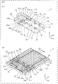
- FIG. 1 is an external perspective view showing a waveguide filter circuit according to Embodiment 1.
- FIG. 2A is an external perspective view of the waveguide filter according to the first embodiment when viewed from the back surface
- FIG. 2B is an external perspective view of the mounting substrate according to the first embodiment.
- FIG. 3 is a bottom view of the waveguide filter according to the first exemplary embodiment.
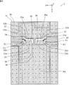
- FIG. 4 is a plan view of the mounting substrate according to the first embodiment.
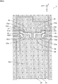
- FIG. 5A is a plan view of the mounting board according to Embodiment 1, and shows a state in which an input / output pattern and a ground pattern are formed on the board body.
- FIG. 5B is a plan view of the mounting substrate according to Embodiment 1, and shows a state in which an input / output pattern, a ground pattern, and a resist are formed on the substrate body.
- FIG. 5C is a plan view of the mounting substrate according to Embodiment 1, and shows a state in which an input / output pattern, a ground pattern, a resist, and solder are formed on the substrate body.
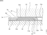
- 6 is a diagram schematically showing a cross section of a part of the waveguide filter circuit according to the first embodiment, and is a diagram showing a cross section taken along the line VI-VI in FIG.
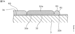
- FIG. 7A is a diagram schematically showing a partial cross section of the mounting substrate according to the first exemplary embodiment.
- FIG. 7B is a diagram showing a state immediately after the waveguide filter is mounted on the mounting substrate shown in FIG. 7A.
- FIG. 8A is a plan view of a mounting board according to Modification 1 of Embodiment 1.
- FIG. 8B is a plan view of the mounting board according to the second modification of the first embodiment.
- FIG. 9 is a plan view of a mounting board according to the third modification of the first embodiment.
- FIG. 10 is a perspective view of the waveguide filter according to the second embodiment viewed from the back side.
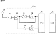
- FIG. 11A is a circuit diagram showing a high-frequency front-end circuit and its peripheral circuits according to Embodiment 3.
- FIG. 11B is a circuit diagram showing a high-frequency front end circuit according to a modification of the third embodiment.
- FIG. 11C is a circuit diagram showing a high-frequency front-end circuit according to another modification of the third embodiment.
- FIG. 12A is a circuit diagram showing a Massive MIMO system according to Embodiment 4.
- FIG. 12B is a plan view of the antenna device of the Massive MIMO system according to Embodiment 4.
- FIG. 1 is an external perspective view showing a waveguide filter circuit 1 according to the first embodiment.
- 2A is an external perspective view of the waveguide filter viewed from the back surface (mounting surface), and
- FIG. 2B is an external perspective view of the mounting substrate.
- the waveguide filter circuit 1 includes a waveguide filter 2 and a mounting substrate 3 on which the waveguide filter 2 is mounted.
- the waveguide filter 2 is fixed to the mounting substrate 3 via a plurality of solder portions including a solder material.
- the waveguide filter 2 is connected to a pair of input / output electrodes 22 formed on the mounting surface 2a and one end (inner end) 22b of each of the pair of input / output electrodes 22.
- a ground electrode 23 is provided on the outer surface including the mounting surface 2a. The ground electrode 23 is disposed in the signal propagation direction of the input / output electrode 22 and is connected to the input / output electrode 22.
- the mounting substrate 3 faces a pair of input / output electrodes 22 of the waveguide filter 2 and has a pair of input / output patterns 32 having a shape corresponding to the pair of input / output electrodes 22. And a ground pattern 33 connected to one end (inner end) 32b of each of the pair of input / output patterns 32.
- the ground pattern 33 is arranged in the signal propagation direction of the input / output pattern 32 and is connected to the input / output pattern 32.
- the input / output pattern 32 of the mounting substrate 3 and the input / output electrode 22 of the waveguide filter 2 are connected via a first solder part S1 containing a solder material.
- a dam portion D1 having a melting point higher than that of the solder material is provided between the input / output pattern 32 or ground pattern 33 of the mounting substrate 3 and the input / output electrode 22 or ground electrode 23 of the waveguide filter 2, a dam portion D1 having a melting point higher than that of the solder material is provided. .
- the dam part D1 is located in the direction from the input / output pattern 32 side to the ground pattern 33 side, and is in contact with the first solder part S1 than the first solder part S1.
- the dam portion D1 is provided at least one of the input / output pattern 32 and the ground pattern 33 and the input / output electrode 22 and the ground electrode 23. Therefore, it can suppress that the solder material of 1st solder part S1 flows into the ground pattern 33 side. Thereby, the shortage of the solder amount between the input / output electrode 22 and the input / output pattern 32 can be suppressed, and the characteristic deterioration of the waveguide filter circuit 1 can be suppressed.
- the waveguide filter circuit 1 includes the waveguide filter 2 and the mounting substrate 3.
- FIG. 3 is a bottom view of the waveguide filter 2.
- the waveguide filter 2 includes a plurality of resonators 7a, 7b, 7c, 7d, 7e, 7f, 7g, and 7h.
- the plurality of resonators 7a to 7h are coupled to each other through the coupling window 8 shown in FIG.
- the waveguide filter 2 according to the present embodiment includes a first resonance unit 5 including four resonators 7a to 7d and a second resonance unit 6 including four resonators 7e to 7h. .
- opposing side electrodes are bonded to each other by a conductive bonding material.
- the waveguide filter 2 includes a filter body 21, a pair of input / output electrodes 22, and a ground electrode 23.
- the filter body 21 includes a dielectric material such as crystal or ceramic.
- the pair of input / output electrodes 22 and the ground electrode 23 include a conductor material mainly composed of Ag.
- the pair of input / output electrodes 22 are formed on the mounting surface 2a of the waveguide filter 2 (the main surface facing the first main surface 3a of the mounting substrate 3 during mounting).
- the pair of input / output electrodes 22 has a constant width and is bent at a part in the longitudinal direction.
- the pair of input / output electrodes 22 has an outer end portion 22a positioned on the outer side and an inner end portion 22b positioned on the inner side of the outer end portion 22a when viewed from the center of each of the resonators 7a and 7h. .
- the outer end 22 a is an open end, and the inner end 22 b is connected to the ground electrode 23.
- the input / output electrode 22 of the resonator 7a has the same configuration as the input / output electrode 22 of the resonator 7a.
- An exposed side surface portion 29 where no conductor film is formed is provided on the side surface 2b of the resonator 7a.
- the outer end portion 22a of the input / output electrode 22 starts from a ridge line (lower corner) formed by the exposed side surface portion 29 and the mounting surface 2a, or a position slightly inside the ridge line.
- the input / output electrode 22 is drawn out in the X direction (direction perpendicular to the exposed side surface portion 29) from the outer end 22a, bent in the middle of the resonator 7a, and extended to the inner end 22b. .
- the ground electrode 23 is formed so as to cover a predetermined region other than the input / output electrode 22 on the outer surface composed of the mounting surface 2a, the side surface 2b, and the top surface 2c. Between the input / output electrode 22 and the ground electrode 23, there are provided a first gap portion 25a and a second gap portion 25b in which the filter body 21 is exposed without forming a conductor film.
- Each of the first gap portion 25 a and the second gap portion 25 b is formed along the inner end portion 22 b from the outer end portion 22 a of the input / output electrode 22 and further formed so as to cut into a part of the ground electrode 23.
- the ground electrode 23a between the gaps sandwiched between the first gap portion 25a and the second gap portion 25b has a rectangular shape and is wider than the input / output electrode 22. Specifically, the ground electrode 23a between the gaps has a rectangular corner connected to the inner end 22b of the input / output electrode 22, and the width gradually increases from the corner toward the center of the rectangular shape. Yes.
- the input / output electrode 22 and the ground electrode 23a between the gaps existing in a region sandwiched between the first gap portion 25a and the second gap portion 25b are referred to as a mode conversion portion 26.
- the transmission signal is converted from the TEM mode to the TE mode or from the TE mode to the TEM mode by the mode conversion unit 26.
- the signal conversion in the mode conversion unit 26 is stabilized, and the characteristic deterioration of the waveguide filter circuit 1 can be suppressed.
- FIG. 4 is a plan view of the mounting substrate 3.
- the mounting board 3 includes a board body 31, a pair of input / output patterns 32, a ground pattern 33, a first solder part S1, and a dam part D1. ing.
- the substrate body 31 includes an organic material having a high Q value.
- the substrate body 31 is not limited to an organic material, and may be formed of a ceramic material.
- the pair of input / output patterns 32, the ground pattern 33, and the via conductors 38 include a conductor material mainly composed of Cu.
- the first solder part S1 is formed of a solder material containing Sn or the like.
- As the dam part D1 for example, a material having a higher melting point than the solder material, such as a green resist, or a material having low wettability with respect to the solder material is used.
- the mounting substrate 3 has a coplanar structure, and includes an input / output pattern 32 formed on the first main surface 3 a and a ground pattern 33 surrounding the input / output pattern 32.
- the mounting board 3 also has a ground pattern 37 on the second main surface (back surface) 3b facing away from the first main surface 3a.
- the ground pattern 33 on the first main surface 3 a and the ground pattern 37 on the second main surface 3 b are connected by a plurality of via conductors 38.
- FIG. 5A is a plan view of the mounting substrate 3 and shows a state in which the input / output pattern 32 and the ground pattern 33 are formed on the substrate body 31.
- the pair of input / output patterns 32 has a shape corresponding to the input / output electrodes 22 of the waveguide filter 2. That is, the pair of input / output patterns 32 has a constant width and is bent at a part in the longitudinal direction.
- the pair of input / output patterns 32 includes an outer end portion 32a positioned on the outer side as viewed from the center of the mounting area MA on which the waveguide filter 2 is mounted, and an inner end portion 32b positioned on the inner side of the outer end portion 32a. have.
- the outer end 32 a is connected to a transmission line 39 connected to an external device, and the inner end 32 b is connected to the ground pattern 33.
- the length of the input / output pattern 32 is, for example, about 0.1 ⁇ at the use frequency of the waveguide filter circuit 1.
- the input / output pattern 32 corresponding to the input / output electrode 22 of the resonator 7a out of the pair of input / output patterns 32 will be described as a representative example.
- the input / output pattern 32 corresponding to the input / output electrode 22 of the resonator 7h has a similar configuration.
- the outer end portion 32a of the input / output pattern 32 starts from the outer edge portion MA1 of the mounting area MA intersecting with the transmission line 39 or a position slightly inside from the outer edge portion MA1.
- the input / output pattern 32 is drawn out from the outer end portion 32a in the X direction (the same direction as the longitudinal direction of the transmission line 39), bends in the middle of the mounting area MA, and extends to the inner end portion 32b. ing.
- the ground pattern 33 is formed so as to cover a predetermined area other than the input / output pattern 32 in the first main surface 3a. Between the input / output pattern 32 and the ground pattern 33, there are provided a first gap portion 35a and a second gap portion 35b in which the substrate body 31 is exposed without forming a conductor pattern.
- Each of the first gap portion 35a and the second gap portion 35b is formed along the inner end portion 32b from the outer end portion 32a of the input / output pattern 32, and further formed so as to cut into a part of the ground pattern 33.
- the ground pattern 33a between the gaps sandwiched between the first gap part 35a and the second gap part 35b is rectangular and wider than the input / output pattern 32. Specifically, the ground pattern 33a between the gaps has a rectangular corner connected to the inner end 32b of the input / output pattern 32, and the width gradually increases from the corner toward the center of the rectangular shape.
- the via conductor 38 is not directly connected to the ground pattern 33a between the gaps, and the via conductor 38 is connected to the ground pattern 33 in a region other than the gap.
- the input / output pattern 32 and the ground pattern 33a between the gaps existing in the region sandwiched between the first gap portion 35a and the second gap portion 35b are referred to as a mode conversion portion 36.
- the transmission signal is converted from the TEM mode to the TE mode or from the TE mode to the TEM mode by the mode conversion unit 36.
- FIG. 5B is a diagram showing a state in which the input / output pattern 32, the ground pattern 33, and the resist (parts indicated by 45 ° inclined hatching) excluding the solder are formed on the substrate body 31.
- FIG. 5C is a diagram showing a state in which solder (portion indicated by ⁇ 45 ° inclined hatching) is further formed on the substrate body 31 shown in FIG. 5B.
- FIG. 6 is a diagram schematically showing a cross section of a part of the waveguide filter circuit 1, and is a diagram showing a cross section taken along line VI-VI in FIG.
- the mounting board 3 includes the first solder part S1 and the dam part D1.
- the dam portion D1 is provided between the input / output pattern 32 or the ground pattern 33 of the mounting substrate 3 and the waveguide filter 2 in the height direction (Z direction). Further, as shown in FIG. 5B, the dam portion D1 is provided on the inner end portion 32b of the input / output pattern 32 in the horizontal direction (direction parallel to the XY plane).
- the position where the dam portion D1 is provided is not limited to the inner end portion 32b, and is between the input / output pattern 32 and the ground pattern 33 of the mounting substrate 3 and the signal transmission of the input / output pattern 32 and the ground pattern 33. It may be on the route.
- between the input / output pattern 32 and the ground pattern 33 is an area including the input / output pattern 32 and the ground pattern 33 (a ground pattern 33a between the gaps) but not including the outer end portion 32a of the input / output pattern 32. It means that there is. That is, the dam part D1 should just be provided in the mode conversion part 36 except the outer side edge part 32a.
- the dam part D1 is a part of the resist pattern R1 formed on the mounting substrate 3.
- the width of the dam part D ⁇ b> 1 is desirably the same as the width of the input / output pattern 32 or larger than the width of the input / output pattern 32.
- the height dimension of the dam part D1 is desirably the same as the distance between the mounting substrate 3 and the waveguide filter 2. However, the height dimension of the dam part D1 is not restricted to said space
- the dam part D ⁇ b> 1 only has to protrude from the input / output pattern 32 or the ground pattern 33 toward the waveguide filter 2. Further, the dam portion D1 is not limited to the case where it is disposed on the mounting substrate 3 side as described above, and may be provided on the input / output electrode 22 or the ground electrode 23 and protrude toward the mounting substrate 3.
- the first solder part S ⁇ b> 1 is located between the input / output pattern 32 and the input / output electrode 22, and connects the input / output pattern 32 and the input / output electrode 22.
- the first solder portion S1 is formed on the input / output pattern 32 including the outer end portion 32a except for the inner end portion 32b. That is, the first solder part S1 is located in a direction from the ground pattern 33 side to the input / output pattern 32 side with respect to the dam part D1, and is in contact with the dam part D1. In other words, the dam part D1 is located in the direction from the input / output pattern 32 side to the ground pattern 33 side, and is in contact with the first solder part S1, rather than the first solder part S1.
- FIG. 7A is a diagram schematically showing a partial cross section of the mounting substrate 3.
- FIG. 7B is a diagram showing a state immediately after the waveguide filter 2 is mounted on the mounting substrate 3 shown in FIG. 7A.
- a dam portion D1 is formed between the input / output pattern 32 of the mounting substrate 3 and the ground pattern 33.
- the dam portion D1 is formed on the inner end portion 32b of the input / output pattern 32.
- the dam part D1 is a part of the resist pattern R1 formed on the mounting substrate 3, and is printed by using a mask having a predetermined pattern.
- the outer resist R2 is also formed simultaneously with the dam portion D1.
- the outer resist R2 is formed on the transmission line 39 connected to the input / output pattern 32 outside the outer edge of the mounting area MA of the waveguide filter 2.
- solder paste S1a to be the first solder portion S1 is formed on the input / output pattern 32 of the mounting substrate 3.
- the first solder portion S1 is formed on the input / output pattern 32 including the outer end portion 32a except for the inner end portion 32b.
- the solder paste S1a is printed and formed using a mask having a predetermined pattern.
- the waveguide filter 2 is mounted on the mounting substrate 3.
- the input / output pattern 32 of the mounting substrate 3 is arranged so as to be connected to the input / output electrodes 22 of the waveguide filter 2.
- the mounting substrate 3 on which the waveguide filter 2 is mounted is reflowed.
- the input / output pattern 32 and the input / output electrode 22 are joined via the first solder portion S1.
- the heated solder paste S1a is once melted, but is dammed up by the adjacent dam portion D1, and does not move to the ground pattern 33 side from the dam portion D1.
- the shortage of the solder amount between the input / output electrode 22 and the input / output pattern 32 can be suppressed, and the characteristic deterioration of the waveguide filter circuit 1 can be suppressed.
- a waveguide filter circuit 1 includes a waveguide filter 2 and a mounting substrate 3 on which the waveguide filter 2 is mounted.
- the waveguide filter 2 is mainly connected to the mounting substrate 3 side.
- An input / output electrode 22 formed on the mounting surface 2a, which is a surface, and a ground electrode 23 formed on the mounting surface 2a are provided.
- the mounting substrate 3 includes an input / output pattern 32 that faces the input / output electrode 22 and has a shape corresponding to the input / output electrode 22, and a ground pattern 33 that is connected to one end 32 b of the input / output pattern 32.
- the input / output pattern 32 and the input / output electrode 22 are connected via a first solder portion S1 containing a solder material.
- a dam portion D ⁇ b> 1 is provided between at least one of the input / output pattern 32 and the ground pattern 33 and between the input / output electrode 22 and the ground electrode 23.
- the dam portion D1 is provided between the input / output pattern 32 or the ground pattern 33 and the input / output electrode 22 or the ground electrode 23 in the height direction, and is more input / output than the first solder portion S1 in the horizontal direction. It is located in the direction from the pattern 32 side toward the ground pattern 33 side, and is in contact with the first solder portion S1.
- This structure can suppress the solder material of the first solder portion S1 from flowing into the ground pattern 33 side or the ground electrode 23 side. For example, when the input / output electrode 22 and the ground electrode 23 are connected and connected, or when the input / output pattern 32 and the ground pattern 33 are connected and connected, there is a solder outflow path. Even if it is a case, the waveguide filter circuit 1 can suppress the inflow of solder by having the dam part D1. Thereby, the shortage of the solder amount between the input / output electrode 22 and the input / output pattern 32 can be suppressed.
- the problem that the outer end 22a of the input / output electrode 22 becomes an open stub can be solved. Thereby, characteristic deterioration of the waveguide filter circuit 1 can be suppressed.
- the waveguide filter mounting substrate 3 includes an input / output pattern 32 having a shape corresponding to the input / output electrode 22 of the waveguide filter 2, a ground pattern 33, and an input / output pattern 32.
- a dam portion D1 is provided between the ground pattern 33 and the input / output pattern 32 and the signal transmission path of the ground pattern 33.
- This structure can suppress the solder material from flowing into the ground pattern 33 when the waveguide filter 2 is mounted on the mounting substrate 3 using solder. Thereby, it is possible to suppress the shortage of the amount of solder between the input / output electrode 22 and the input / output pattern 32 of the waveguide filter 2, and it is possible to suppress the characteristic deterioration of the waveguide filter circuit 1.
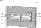
- FIG. 8A is a plan view of a mounting substrate 3A according to Modification 1 of Embodiment 1.
- FIG. 8A is a plan view of a mounting substrate 3A according to Modification 1 of Embodiment 1.
- the dam portion D1 is provided at an intermediate position between the outer end portion 32a and the inner end portion 32b on the input / output pattern 32, as shown in FIG. 8A. That is, the dam portion D1 is provided between the input / output pattern 32 and the ground pattern 33 and on the signal transmission path of the input / output pattern 32 and the ground pattern 33. In this case, the first solder part S1 is provided on the input / output pattern 32 located outside the dam part D1.
- the dam portion D1 can suppress the inflow of solder, and an effect similar to that of the first embodiment can be obtained.
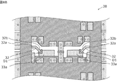
- FIG. 8B is a plan view of mounting substrate 3B according to Modification 2 of Embodiment 1.
- FIG. 8B is a plan view of mounting substrate 3B according to Modification 2 of Embodiment 1.
- Dam part D1 as shown in FIG. 8B, is provided on the ground pattern 33a between the gaps. That is, the dam portion D1 is provided between the input / output pattern 32 and the ground pattern 33 and on the signal transmission path of the input / output pattern 32 and the ground pattern 33. In this case, the first solder part S1 is provided on the ground pattern 33a and the input / output pattern 32 between the gaps located outside the dam part D1.
- the dam portion D1 can suppress the inflow of solder, and an effect similar to that of the first embodiment can be obtained.
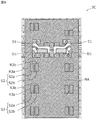
- FIG. 9 is a plan view of a mounting substrate 3C according to the third modification of the first embodiment.
- the waveguide filter 2 is fixed to the mounting substrate 3 by a plurality of second solder portions S2, but in the mounting substrate 3 according to the modification 3, the arrangement position of the second solder portion S2 is set as follows. , Improving the fixing strength.
- Each of the plurality of second solder portions S2 according to the modification 3 includes a set of solder portions, that is, a fillet portion S2a and an inner bottom portion S2b.
- the fillet portion S2a is a portion connected to the ground electrode 23 in a partial region of the side surface 2b of the waveguide filter 2 and a partial region of the mounting surface 2a.
- the inner bottom portion S2b is a portion connected to the ground electrode 23 in a region located inside the mounting surface 2a of the waveguide filter 2 rather than the fillet portion S2a.
- the fillet part S2a and the inner bottom part S2b of the second solder part S2 are formed by printing a solder paste on the opening of the resist pattern R1.
- the opening R3a of the resist pattern R1 overlaps the outer edge of the waveguide filter 2 when the mounting substrate 3 on which the waveguide filter 2 is mounted is viewed in plan view.
- a fillet S2a is formed in one opening R3a, and an inner bottom S2b is formed in the other opening R3b.
- the waveguide filter 2 is mounted while suppressing the solder from flowing into the mounting surface 2a in the fillet portion S2a by configuring the second solder portion S2 with the fillet portion S2a and the inner bottom portion S2b. It can be fixed to the substrate 3. Further, by providing the inner bottom portion S2b at a location different from the fillet portion S2a, the fixing strength between the waveguide filter 2 and the mounting substrate 3 can be further improved. Moreover, since the position of the fillet portion S2a is fixed by forming the resist pattern R1 having the opening portion R3a and forming the fillet portion S2a in the opening portion R3a, the inflow of solder can be suppressed.
- FIG. 10 is a perspective view of the waveguide filter 2A according to the second embodiment as viewed from the back surface (mounting surface).
- the dam portion D2 is provided not on the mounting substrate 3 but on the waveguide filter 2.
- the waveguide filter 2A includes an input / output electrode 22 formed on the mounting surface 2a and a ground electrode 23 formed on an outer surface including the mounting surface 2a so as to be connected to one end 22b of the input / output electrode 22. ing.
- the dam portion D2 is provided on the inner end portion 22b of the input / output electrode 22.
- the position where the dam portion D2 is provided is not limited to the inner end portion 22b of the input / output electrode 22, but is between the input / output electrode 22 and the ground electrode 23 and the signals of the input / output electrode 22 and the ground electrode 23. It may be on the transmission path.
- between the input / output electrode 22 and the ground electrode 23 is a region including the input / output electrode 22 and the ground electrode 23 (the ground electrode 23a between the gaps) but not including the outer end portion 22a of the input / output electrode 22. It means that there is. That is, the dam part D2 should just be provided in the mode conversion part 26 except the outer side edge part 22a.
- the dam portion D2 the same material as the resist pattern R1 formed on the mounting substrate 3 is used.
- the width of the dam part D ⁇ b> 2 is desirably the same as the width of the input / output electrode 22 or larger than the width of the input / output electrode 22.
- the height dimension of the dam part D2 is desirably the same as the distance between the mounting substrate 3 and the waveguide filter 2A. However, the height dimension of the dam part D2 is not limited to the above-described interval.
- the solder material when the waveguide filter 2A is mounted on the mounting substrate 3 using solder, the solder material can be prevented from flowing into the ground electrode 23 side (or the ground pattern 33 side). . As a result, it is possible to suppress an insufficient amount of solder between the input / output electrode 22 and the input / output pattern 32 of the mounting substrate 3, and to suppress deterioration in characteristics of the waveguide filter circuit 1.
- a solder part may be formed in the waveguide filter 2A. That is, the solder part of the waveguide filter 2A may be located in a direction from the ground electrode 23 side toward the input / output electrode 22 side with respect to the dam part D2, and may be formed in contact with the dam part D2.
- FIG. 11A is a circuit diagram showing a high-frequency front-end circuit 50A and its peripheral circuits according to the third embodiment. The figure shows a high-frequency front-end circuit 50A, an antenna element 53, an RF signal processing circuit 91, and a baseband signal processing circuit 92.
- the high-frequency front end circuit 50A includes filters 61, 62 and 63, a switch circuit 70, a power amplifier circuit 81, and a low noise amplifier circuit 82.
- the power amplifier circuit 81 is a transmission amplifier circuit that amplifies the high-frequency transmission signal output from the RF signal processing circuit 91 and outputs the amplified signal to the antenna element 53 via the switch circuit 70 and the filter 61.
- the low noise amplifier circuit 82 is a reception amplification circuit that amplifies a high frequency signal that has passed through the antenna element 53, the filter 61, and the switch circuit 70 and outputs the amplified signal to the RF signal processing circuit 91.
- the filter 61 is connected to the antenna element 53 and is, for example, an antenna filter that selectively passes high-frequency signals in the transmission band and the reception band.
- the filter 62 is an interstage filter that is disposed between the power amplifier circuit 81 and the RF signal processing circuit 91 and selectively passes high-frequency signals in the transmission band.
- the filter 63 is an interstage filter that is disposed between the low-noise amplifier circuit 82 and the RF signal processing circuit 91 and selectively passes a high-frequency signal in the reception band.
- the switch circuit 70 is a switch for switching the connection between the antenna element 53 and the transmission signal path and the reception signal path.
- the RF signal processing circuit 91 processes a high-frequency reception signal input from the antenna element 53 via the reception signal path by down-conversion or the like, and a baseband signal processing circuit 92 receives the reception signal generated by the signal processing. Output to.
- the RF signal processing circuit 91 is, for example, an RFIC (Radio Frequency Integrated Circuit). Further, the RF signal processing circuit 91 performs signal processing on the transmission signal input from the baseband signal processing circuit 92 by up-conversion or the like, and outputs the high-frequency transmission signal generated by the signal processing to the power amplifier circuit 81.
- the signal processed by the baseband signal processing circuit 92 is used, for example, for displaying an image as an image signal or for calling as an audio signal.
- the high-frequency front end circuit 50A may include other circuit elements between the filters 61, 62 and 63, the switch circuit 70, the power amplifier circuit 81, and the low noise amplifier circuit 82.
- FIG. 11B is a circuit diagram showing a high-frequency front end circuit 50B according to a modification.
- the high-frequency front-end circuit 50B has a circulator 71, the switch circuit 72 is terminated at 50 ohms during transmission, and the switch circuit 72 is low-noise amplifier circuit 82 during reception.
- the circuit structure connected to the side may be sufficient.
- FIG. 11C is a circuit diagram showing a high-frequency front-end circuit 50C according to another modification.
- the high-frequency front-end circuit 50C may have a circuit configuration in which the third port of the circulator 73 is terminated to be an isolator.
- the waveguide filters shown in the first and second embodiments and the modifications thereof are used as the filters 61, 62, and 63. it can.
- the phantom cell is a network configuration that separates a control signal for ensuring communication stability between a macro cell in a low frequency band and a small cell in a high frequency band and a data signal that is a target of high-speed data communication.
- Each phantom cell is provided with a Massive MIMO antenna device.
- the Massive MIMO system is a technique for improving transmission quality in a millimeter wave band or the like, and controls the directivity of the antenna element by controlling a signal transmitted from each antenna element.
- the Massive MIMO system uses a large number of antenna elements, and therefore can generate a sharp directional beam.
- By increasing the directivity of the beam it is possible to fly radio waves to some extent even in a high frequency band, and it is possible to reduce the interference between cells and increase the frequency utilization efficiency.
- FIG. 12A is a circuit diagram showing a Massive MIMO system according to Embodiment 4.
- FIG. 12B is a plan view of the antenna device of the Massive MIMO system according to Embodiment 4.
- the antenna device 51 shown in FIG. 12B is used in the Massive MIMO system shown in FIG. 12A.
- the antenna device 51 includes a plurality of patch antennas 52 arranged in a matrix.
- FIG. 12A is a diagram illustrating a configuration of a high-frequency front-end circuit 50D including the antenna device 51.
- the high-frequency front end circuit 50D is a Massive MIMO system according to the present embodiment.
- the patch antenna 52 is connected with band-pass filters 61a, 61b and 61c.
- a switch circuit 70a is connected between the filter 61a, the power amplifier circuit 81a, and the low noise amplifier circuit 82a.
- a switch circuit 70b is connected between the filter 61b, the power amplifier circuit 81b, and the low noise amplifier circuit 82b.
- a switch circuit 70c is connected between the filter 61c and the power amplifier circuit 81c and the low noise amplifier circuit 82c.
- the low noise amplifier circuits 82a, 82b and 82c are connected to the baseband signal processing circuit 92.
- a band-pass filter 62a and a mixer 94a are connected between the baseband signal processing circuit 92 and the power amplifier circuit 81a.
- a band-pass filter 62b and a mixer 94b are connected between the baseband signal processing circuit 92 and the power amplifier circuit 81b.
- a band pass filter 62c and a mixer 94c are connected between the baseband signal processing circuit 92 and the power amplifier circuit 81c.
- a local oscillator 93 is connected to the mixers 94a, 94b and 94c.
- the local oscillator 93 outputs a reference frequency for up-conversion to a high frequency and down-conversion to a low frequency in the mixers 94a to 94c to the mixers 94a to 94c.
- the switches below the Switch can be incorporated into the RFIC and can be one. Alternatively, as shown in FIG. 11A, the part below the mixer may be taken into the RFIC.
- Filters 61a to 61c pass the transmission / reception frequency band and remove other frequency components.
- the switch circuits 70a to 70c switch between a transmission signal and a reception signal.
- the filters 62a to 62c pass the frequency band of the transmission signal and remove other frequency components.
- the waveguide filters 61a to 61c and 62a to 62c the waveguide filters according to the first and second embodiments and modifications thereof can be used.
- the filters 61a to 61c connected to the patch antenna 52 may be disposed on the back surface of the substrate on which the patch antenna 52 is formed.
- an antenna device 51 including a patch antenna 52 with filters 61a to 61c is configured.
- filter characteristics variation is suppressed in the filters 61a to 61c and 62a to 62c, so that a Massive MIMO system with reduced high-frequency characteristic variation is realized. It becomes possible.
- the waveguide filter circuit and the like according to the embodiment of the present invention have been described with reference to the embodiment and the modification.
- the waveguide filter circuit and the like according to the present invention are the same as those in the embodiment and the modification. It is not limited.
- Various devices incorporating the obtained modified examples and the waveguide filter circuit of the present disclosure are also included in the present invention.
- the waveguide filter 2 in which the input / output electrode 22 and the ground electrode 23 are continuously connected, and the mounting substrate 3 in which the input / output pattern 32 and the ground pattern 33 are continuously connected are provided.
- the input / output electrode 22 and the ground electrode 23 may be continuously connected, and the input / output pattern 32 and the ground pattern 33 may be separated.
- the input / output electrode 22 and the ground electrode 23 may be separated, and the input / output pattern 32 and the ground pattern 33 may be continuously connected.
- the waveguide filter 2 of the present embodiment may include an input / output electrode 22 and a ground electrode 23 connected to or close to one end of the input / output electrode 22.
- a pattern 32 and a ground pattern 33 connected to or close to one end of the input / output pattern 32 may be provided.
- the waveguide filter according to the embodiment and its modification can also be applied as a dielectric waveguide duplexer or a dielectric waveguide multiplexer.
- the waveguide filter circuit of the present invention can be widely used in communication devices such as a millimeter wave mobile communication system and a Massive MIMO system.
Landscapes
- Engineering & Computer Science (AREA)
- Microelectronics & Electronic Packaging (AREA)
- Control Of Motors That Do Not Use Commutators (AREA)
Abstract
導波管フィルタ(2)が実装基板(3)に実装された導波管フィルタ回路(1)であって、導波管フィルタ(2)は、実装面(2a)に形成された入出力電極(22)と、実装面(2a)に形成されたグランド電極(23)とを備え、実装基板(3)は、入出力パターン(32)と、グランドパターン(33)とを備える。入出力パターン(32)と入出力電極(22)とは、第1はんだ部(S1)を介して接続されている。入出力パターン(32)とグランドパターン(33)との間、および、入出力電極(22)とグランド電極(23)との間のうち少なくとも一方には、ダム部(D1)が設けられている。
Description
本発明は、導波管フィルタが実装された実装基板を備える導波管フィルタ回路、導波管フィルタ用実装基板、および、導波管フィルタに関する。
従来、TE(Transverse Electric)モードの導波管共振器を複数結合して、所望の周波数特性を得る導波管フィルタが知られている。
特許文献1には、複数の誘電体共振器を有する導波管フィルタと、この導波管フィルタを実装する実装基板とを備える導波管フィルタ回路が開示されている。導波管フィルタは、実装基板側の主面である実装面に形成された一対の入出力電極と、実装面に形成されたグランド電極とを備えている。実装基板は、導波管フィルタの入出力電極に対応する形状を有する一対の入出力パターンと、グランドパターンとを備えている。
しかしながら、特許文献1に記載された導波管フィルタでは、はんだを用いて導波管フィルタを実装基板に実装した際に、はんだが、入出力電極をつたってグランド電極およびグランドパターンへ流れ込む場合がある。はんだの流れ込み量が多くなると、入出力電極と入出力パターンとの間のはんだ量が不足し、導波管フィルタ回路の特性が劣化するという問題が起こり得る。
本発明は、上記問題を解決するものであり、導波管フィルタの入出力電極と実装基板の入出力パターンとの間のはんだ量不足を抑制し、導波管フィルタ回路の特性劣化を抑制することを目的とする。
上記目的を達成するために、本発明の一態様に係る導波管フィルタ回路は、導波管フィルタと、前記導波管フィルタが実装された実装基板とを備える導波管フィルタ回路であって、前記導波管フィルタは、前記実装基板側の主面である実装面に形成された入出力電極と、前記実装面に形成されたグランド電極と、を備え、前記実装基板は、前記入出力電極に対応する形状を有する入出力パターンと、グランドパターンと、を備え、前記入出力パターンと前記入出力電極とは、はんだ材料を含む第1はんだ部を介して接続され、前記入出力パターンと前記グランドパターンとの間、および、前記入出力電極と前記グランド電極との間のうち少なくとも一方には、ダム部が設けられている。
このように、ダム部が、入出力パターンとグランドパターンとの間、および、入出力電極とグランド電極との間のうち少なくとも一方に設けられているので、第1はんだ部のはんだ材料が、グランドパターン側へ流れ込むことを抑制することができる。これにより、入出力電極と入出力パターンとの間のはんだ量不足を抑制し、導波管フィルタ回路の特性劣化を抑制することができる。
また、前記ダム部は、前記第1はんだ部よりも、前記入出力パターン側から前記グランドパターン側へ向かう方角に位置し、前記第1はんだ部に接していてもよい。
このように、ダム部が、第1はんだ部よりも、入出力パターンからグランドパターン側へ向かう方角に位置し、第1はんだ部に接しているので、第1はんだ部のはんだ材料が、グランドパターン側へ流れ込むことを抑制することができる。これにより、入出力電極と入出力パターンとの間のはんだ量不足を抑制し、導波管フィルタ回路の特性劣化を抑制することができる。
また、前記ダム部は、前記入出力パターンと前記グランドパターンとの間であって、前記入出力パターンおよび前記グランドパターンの信号伝送経路上に配置されていてもよい。
これによれば、第1はんだ部のはんだ材料が、信号伝送経路上をつたってグランドパターン側へ流れ込むことを抑制することができる。これにより、入出力電極と入出力パターンとの間のはんだ量不足を抑制し、導波管フィルタ回路の特性劣化を抑制することができる。
また、前記ダム部は、前記実装基板に形成されるレジストパターンの一部であってもよい。
このようにダム部をレジストで形成することで、実装時のはんだ材料の流れ込みを抑制することができる。また、実装基板へのレジストパターン形成と同時にダム部を形成することが可能となり、生産効率の低下を抑制することができる。
また、前記ダム部は、前記はんだ材料よりも融点が高くてもよい。
これにより、例えば、はんだリフローを行って、はんだ材料を溶融させた場合であっても、ダム部の固化状態を維持することができ、はんだの流れ込みを抑制することができる。
また、前記入出力パターンの幅よりも、信号伝搬方向において前記入出力パターンに接続する前記グランドパターンの幅のほうが大きくてもよい。
このように、入出力パターンよりも幅が大きいダム部を用いることで、はんだ材料の流れ込みをさらに抑制することができる。
また、前記入出力パターンまたは前記グランドパターンは、信号を、TEMモードからTEモードまたはTEモードからTEMモードに変換するモード変換部を有し、前記ダム部は、前記モード変換部に設けられていてもよい。
これによれば、モード変換部におけるはんだ量不足を抑制し、導波管フィルタ回路の特性劣化を抑制することができる。
また、前記グランド電極は、前記グランドパターンに、はんだ材料を含む複数の第2はんだ部を介して接続されていてもよい。
これによれば、導波管フィルタと実装基板との固着強度を向上することができる。
また、前記複数の第2はんだ部のそれぞれは、前記導波管フィルタの側面の一部領域および前記実装面の一部領域の前記グランド電極に接続するフィレット部と、前記フィレット部よりも、前記導波管フィルタの前記実装面の内側に位置する領域の前記グランド電極に接続する内側底部とを有していてもよい。
このように、第2はんだ部を、フィレット部および内側底部で構成することで、フィレット部における、実装面へのはんだの流れ込みを抑制しつつ、導波管フィルタを実装基板に固定することができる。また、内側底部をフィレット部と異なる箇所に設けることで、導波管フィルタと実装基板との固着強度をさらに向上させることができる。
また、前記実装基板の前記グランドパターン上には、開口部を有するレジストパターンが形成され、前記開口部は、前記導波管フィルタが実装された前記実装基板を平面視した場合に、前記導波管フィルタの外縁と重なり、前記開口部には、前記第2はんだ部の前記フィレット部が形成されていてもよい。
このように、開口部を有するレジストパターンを形成し、開口部にフィレット部を形成することで、フィレット部の水平方向の位置が固定されるので、はんだの流れ込みを抑制することができる。
また、本発明の一態様に係る導波管フィルタ用実装基板は、入出力電極およびグランド電極を備える導波管フィルタを実装するための実装基板であって、前記導波管フィルタの前記入出力電極に対応する形状を有する入出力パターンと、グランドパターンと、前記入出力パターンと前記グランドパターンとの間であって、前記入出力パターンおよび前記グランドパターンの信号伝送経路上に配置されたダム部と、を備える。
これによれば、導波管フィルタを、はんだを用いて実装基板に実装した場合に、はんだ材料が、グランドパターン側へ流れ込むことを抑制することができる。これにより、導波管フィルタの入出力電極と入出力パターンとの間のはんだ量不足を抑制することができ、導波管フィルタ回路の特性劣化を抑制することが可能となる。
また、前記実装基板の前記入出力パターン上および前記グランドパターン上には、所定形状を有するレジストパターンが形成され、前記ダム部は、前記レジストパターンの一部であってもよい。
このようにダム部をレジストで形成することで、実装時のはんだ材料の流れ込みを抑制することができる。また、実装基板のレジストパターンと同時にダム部を形成することができるので、生産効率の低下を抑制することができる。
また、本発明の一態様に係る導波管フィルタは、実装面に形成された入出力電極と、前記実装面に形成されたグランド電極と、前記入出力電極と前記グランド電極との間であって、前記入出力電極および前記グランド電極の信号伝送経路上に配置されたダム部と、を備える。
この構造により、導波管フィルタを、はんだを用いて実装基板に実装した場合に、はんだ材料が、グランド電極側へ流れ込むことを抑制することができる。これにより、入出力電極と実装基板の入出力パターンとの間のはんだ量不足を抑制することができ、導波管フィルタ回路の特性劣化を抑制することが可能となる。
本発明によれば、導波管フィルタの入出力電極と実装基板の入出力パターンとの間のはんだ量不足を抑制し、導波管フィルタ回路の特性劣化を抑制することができる。
以下、本発明の実施の形態について、図面を用いて詳細に説明する。なお、以下で説明する実施の形態は、いずれも包括的または具体的な例を示すものである。以下の実施の形態で示される数値、形状、材料、構成要素、構成要素の配置および接続形態などは、一例であり、本発明を限定する主旨ではない。以下の実施の形態における構成要素のうち、独立請求項に記載されていない構成要素については、任意の構成要素として説明される。また、図面に示される構成要素の大きさ、または大きさの比は、必ずしも厳密ではない。
(実施の形態1)
[1.1 導波管フィルタ回路の概要]
まず、導波管フィルタ回路の概要について説明する。
[1.1 導波管フィルタ回路の概要]
まず、導波管フィルタ回路の概要について説明する。
図1は、実施の形態1に係る導波管フィルタ回路1を示す外観斜視図である。図2の(a)は、導波管フィルタを裏面(実装面)から見た外観斜視図であり、図2の(b)は、実装基板の外観斜視図である。
実施の形態1に係る導波管フィルタ回路1は、図1に示すように、導波管フィルタ2と、導波管フィルタ2が実装された実装基板3とにより構成される。導波管フィルタ2は、はんだ材料を含む複数のはんだ部を介して、実装基板3に固定されている。
導波管フィルタ2は、図2の(a)に示すように、実装面2aに形成された一対の入出力電極22と、一対の入出力電極22それぞれの一端(内側端部)22bと接続するように、実装面2aを含む外表面に形成されたグランド電極23とを備えている。グランド電極23は、入出力電極22の信号の伝搬方向に配置され、入出力電極22に接続されている。
実装基板3は、図2の(b)に示すように、導波管フィルタ2の一対の入出力電極22に対向し、一対の入出力電極22に対応する形状を有する一対の入出力パターン32と、一対の入出力パターン32それぞれの一端(内側端部)32bと接続するグランドパターン33とを備えている。グランドパターン33は、入出力パターン32の信号の伝搬方向に配置され、入出力パターン32に接続されている。
実装基板3の入出力パターン32と導波管フィルタ2の入出力電極22とは、はんだ材料を含む第1はんだ部S1を介して接続される。
実装基板3の入出力パターン32またはグランドパターン33と、導波管フィルタ2の入出力電極22またはグランド電極23と、の間には、はんだ材料よりも融点が高いダム部D1が設けられている。ダム部D1は、第1はんだ部S1よりも、入出力パターン32側からグランドパターン33側へ向かう方角に位置しており、第1はんだ部S1に接している。
実施の形態1に係る導波管フィルタ回路1では、ダム部D1が、入出力パターン32とグランドパターン33との間、および、入出力電極22とグランド電極23との間のうち少なくとも一方に設けられているので、第1はんだ部S1のはんだ材料が、グランドパターン33側へ流れ込むことを抑制することができる。これにより、入出力電極22と入出力パターン32との間のはんだ量不足を抑制し、導波管フィルタ回路1の特性劣化を抑制することができる。
[1.2 導波管フィルタ回路の各構成の説明]
前述したように、導波管フィルタ回路1は、導波管フィルタ2と実装基板3とを備えている。
前述したように、導波管フィルタ回路1は、導波管フィルタ2と実装基板3とを備えている。
まず、導波管フィルタ2について説明する。図3は、導波管フィルタ2の底面図である。
導波管フィルタ2は、図1および図3に示すように、複数の共振器7a、7b、7c、7d、7e、7f、7g、7hを備えている。複数の共振器7a~7hは、図1に示す結合窓8を介して相互に結合されている。なお、本実施の形態における導波管フィルタ2は、4つの共振器7a~7dからなる第1共振部5と、4つの共振器7e~7hからなる第2共振部6とにより構成されている。第1共振部5および第2共振部6は、対向する側面電極(グランド電極)が、導電性接合材によって互いに接合されている。
導波管フィルタ2は、フィルタ本体21と、一対の入出力電極22と、グランド電極23とを備えている。
フィルタ本体21は、水晶またはセラミックなどの誘電体材料を含む。一対の入出力電極22およびグランド電極23は、Agを主成分とする導体材料を含む。
一対の入出力電極22は、導波管フィルタ2の実装面2a(実装時において実装基板3の第1主面3aと対向する主面)に形成されている。一対の入出力電極22は、幅が一定であり、長手方向の一部分で屈曲している。一対の入出力電極22は、共振器7a、7hそれぞれの中心から見て、外側に位置する外側端部22aと、外側端部22aよりも内側に位置する内側端部22bとを有している。外側端部22aは開放端であり、内側端部22bはグランド電極23に接続されている。
以下、一対の入出力電極22のうち、共振器7aの入出力電極22を代表例に挙げて説明する。なお、共振器7hの入出力電極22も、共振器7aの入出力電極22と同様の構成を有している。
共振器7aの側面2bには、導体膜が形成されていない露出側面部29が設けられている。入出力電極22の外側端部22aは、露出側面部29と実装面2aとにより形成される稜線(下の角)、または、この稜線からわずかに内側に入った位置を起点としている。入出力電極22は、外側端部22aからX方向(露出側面部29と垂直な方向)に引き出され、途中で共振器7aの中心方向に折れ曲がり、内側端部22bまで延びるように形成されている。
グランド電極23は、実装面2a、側面2b、天面2cからなる外表面のうちの、入出力電極22以外の所定領域を覆うように形成されている。入出力電極22とグランド電極23との間には、導体膜が形成されずにフィルタ本体21が露出している第1ギャップ部25aおよび第2ギャップ部25bが設けられている。
第1ギャップ部25aおよび第2ギャップ部25bのそれぞれは、入出力電極22の外側端部22aから内側端部22bに沿って形成され、さらに、グランド電極23の一部に切れ込むように形成されている。第1ギャップ部25aおよび第2ギャップ部25bに挟まれたギャップ間のグランド電極23aは、長方形状であり、入出力電極22よりも幅が広い。具体的には、ギャップ間のグランド電極23aは、長方形形状をした角部が入出力電極22の内側端部22bに接続され、角部から長方形形状の中心に向かって、幅が徐々に広がっている。
ここで、第1ギャップ部25aおよび第2ギャップ部25bに挟まれた領域に存在する入出力電極22およびギャップ間のグランド電極23aを、モード変換部26と呼ぶ。導波管フィルタ2では、このモード変換部26にて、伝送信号がTEMモードからTEモードまたはTEモードからTEMモードに変換される。入出力電極22のはんだ接合ばらつきを小さくすることで、モード変換部26における信号変換が安定化し、導波管フィルタ回路1の特性劣化を抑制することができる。
次に、実装基板3について説明する。図4は、実装基板3の平面図である。
実装基板3は、図2の(b)および図4に示すように、基板本体31と、一対の入出力パターン32と、グランドパターン33と、第1はんだ部S1と、ダム部D1とを備えている。
基板本体31は、Q値が高い有機材料を含む。基板本体31は、有機材料に限られず、セラミック材料により形成されていてもよい。一対の入出力パターン32、グランドパターン33およびビア導体38は、Cuを主成分とする導体材料を含む。第1はんだ部S1は、Snなどを含むはんだ材料により形成されている。ダム部D1としては、例えばグリーンレジストのように、はんだ材料より融点が高い材料、また、はんだ材料に対する濡れ性が低い材料が用いられる。
実装基板3は、コプレーナ構造を有し、第1主面3aに形成された入出力パターン32と、入出力パターン32を囲むグランドパターン33とにより構成される。また、実装基板3は、第1主面3aと背向する第2主面(裏面)3bにもグランドパターン37を有している。第1主面3aのグランドパターン33と第2主面3bのグランドパターン37は、複数のビア導体38により接続されている。
図5Aは、実装基板3の平面図であって、基板本体31に入出力パターン32およびグランドパターン33が形成された状態を示す図である。
一対の入出力パターン32は、導波管フィルタ2の入出力電極22に対応する形状を有している。すなわち、一対の入出力パターン32は、幅が一定であり、長手方向の一部分で屈曲している。一対の入出力パターン32は、導波管フィルタ2が実装される実装領域MAの中心から見て外側に位置する外側端部32aと、外側端部32aよりも内側に位置する内側端部32bとを有している。外側端部32aは外部機器と接続される伝送線路39に繋がっており、内側端部32bはグランドパターン33に接続されている。入出力パターン32の長さは、例えば、導波管フィルタ回路1の使用周波数において、0.1λ程度である。
以下、一対の入出力パターン32のうち、共振器7aの入出力電極22に対応する入出力パターン32を代表例に挙げて説明する。なお、共振器7hの入出力電極22に対応する入出力パターン32も、同様の構成を有している。
入出力パターン32の外側端部32aは、伝送線路39と交差する実装領域MAの外縁部分MA1、または、この外縁部分MA1からわずかに内側に入った位置を起点としている。入出力パターン32は、外側端部32aからX方向(伝送線路39の長手方向と同じ方向)に引き出され、途中で実装領域MAの内部に向けて折れ曲がり、内側端部32bまで延びるように形成されている。
グランドパターン33は、第1主面3aのうちの、入出力パターン32以外の所定領域を覆うように形成されている。入出力パターン32とグランドパターン33との間には、導体パターンが形成されずに基板本体31が露出している第1ギャップ部35aおよび第2ギャップ部35bが設けられている。
第1ギャップ部35aおよび第2ギャップ部35bのそれぞれは、入出力パターン32の外側端部32aから内側端部32bに沿って形成され、さらに、グランドパターン33の一部に切れ込むように形成されている。第1ギャップ部35aおよび第2ギャップ部35bに挟まれたギャップ間のグランドパターン33aは、長方形状であり、入出力パターン32よりも幅が広い。具体的には、ギャップ間のグランドパターン33aは、長方形形状をした角部が入出力パターン32の内側端部32bに接続され、角部から長方形形状の中心に向かって、幅が徐々に広がっている。ギャップ間のグランドパターン33aには、ビア導体38が直接接続されておらず、ギャップ間以外の領域のグランドパターン33にビア導体38が接続されている。
ここで、第1ギャップ部35aおよび第2ギャップ部35bに挟まれた領域に存在する入出力パターン32およびギャップ間のグランドパターン33aを、モード変換部36と呼ぶ。実装基板3では、このモード変換部36にて、伝送信号がTEMモードからTEモードまたはTEモードからTEMモードに変換される。入出力パターン32のはんだ接合ばらつきを小さくすることで、モード変換部36における信号変換が安定化し、導波管フィルタ回路1の特性劣化を抑制することができる。
図5Bは、基板本体31に、はんだを除く、入出力パターン32、グランドパターン33およびレジスト(45°傾斜ハッチングで示す部分)が形成された状態を示す図である。図5Cは、図5Bに示す基板本体31に、さらに、はんだ(-45°傾斜ハッチングで示す部分)が形成された状態を示す図である。図6は、導波管フィルタ回路1の一部の断面を模式的に示す図であって、図4のVI-VI線の位置の断面を示す図である。
前述したように、本実施の形態に係る実装基板3は、第1はんだ部S1とダム部D1とを備えている。
ダム部D1は、図6に示すように、高さ方向(Z方向)において、実装基板3の入出力パターン32またはグランドパターン33と、導波管フィルタ2との間に設けられている。また、ダム部D1は、図5Bに示すように、水平方向(XY面に平行な方向)において、入出力パターン32の内側端部32b上に設けられている。
なお、ダム部D1が設けられる位置は、内側端部32b上に限られず、実装基板3の入出力パターン32とグランドパターン33との間であって、入出力パターン32およびグランドパターン33の信号伝送経路上であればよい。ここで、入出力パターン32とグランドパターン33との間とは、入出力パターン32およびグランドパターン33(ギャップ間のグランドパターン33a)を含み、入出力パターン32の外側端部32aを含まない領域であることを意味する。すなわち、ダム部D1は、外側端部32aを除くモード変換部36に設けられていればよい。
ダム部D1は、実装基板3に形成されるレジストパターンR1の一部である。ダム部D1の幅は、入出力パターン32の幅と同じ、または、入出力パターン32の幅よりも大きいことが望ましい。ダム部D1の高さ寸法は、実装基板3および導波管フィルタ2の間隔と同じであることが望ましい。ただし、ダム部D1の高さ寸法は上記の間隔に限られない。ダム部D1は、入出力パターン32上またはグランドパターン33上から導波管フィルタ2に向けて突出していればよい。また、ダム部D1は、上記のように実装基板3側に配置される場合に限られず、入出力電極22上またはグランド電極23上に設けられ、実装基板3に向けて突出していてもよい。
第1はんだ部S1は、図5Cおよび図6に示すように、入出力パターン32と入出力電極22との間に位置し、入出力パターン32と入出力電極22とを接続する。本実施の形態において、第1はんだ部S1は、内側端部32bを除き、外側端部32aを含む入出力パターン32上に形成されている。すなわち、第1はんだ部S1は、ダム部D1よりも、グランドパターン33側から入出力パターン32側へ向かう方角に位置し、ダム部D1に接している。換言すれば、ダム部D1は、第1はんだ部S1よりも、入出力パターン32側からグランドパターン33側へ向かう方角に位置し、第1はんだ部S1に接している。
[1.3 導波管フィルタ回路の製造方法]
次に、導波管フィルタ回路1の製造方法について説明する。図7Aは、実装基板3の一部の断面を模式的に示す図である。図7Bは、図7Aに示す実装基板3に、導波管フィルタ2を搭載した直後の状態を示す図である。
次に、導波管フィルタ回路1の製造方法について説明する。図7Aは、実装基板3の一部の断面を模式的に示す図である。図7Bは、図7Aに示す実装基板3に、導波管フィルタ2を搭載した直後の状態を示す図である。
まず、図7Aに示すように、実装基板3の入出力パターン32とグランドパターン33との間に、ダム部D1を形成する。本実施の形態では、ダム部D1は、入出力パターン32の内側端部32b上に形成される。ダム部D1は、実装基板3に形成されるレジストパターンR1の一部であり、所定パターンを有するマスクを用いて印刷形成される。
なお、図7Aに示す工程では、ダム部D1と同時に、外側レジストR2も形成している。外側レジストR2は、導波管フィルタ2の実装領域MAの外縁の外側であって、入出力パターン32に繋がっている伝送線路39上に形成される。
次に、実装基板3の入出力パターン32上に、第1はんだ部S1となるはんだペーストS1aを形成する。本実施の形態では、第1はんだ部S1は、内側端部32bを除き、外側端部32aを含む入出力パターン32上に形成される。はんだペーストS1aは、所定パターンを有するマスクを用いて印刷形成される。
次に、図7Bに示すように、実装基板3上に導波管フィルタ2を搭載する。その際、実装基板3の入出力パターン32が、導波管フィルタ2の入出力電極22に接続するように配置される。その後、導波管フィルタ2が搭載された実装基板3をリフローする。
リフロー後、図6に示すように、入出力パターン32と入出力電極22とが、第1はんだ部S1を介して接合される。その際、加熱されたはんだペーストS1aは一旦溶融するが、隣接するダム部D1に堰きとめられ、ダム部D1よりもグランドパターン33側に移動しないようになっている。これにより、入出力電極22と入出力パターン32との間のはんだ量不足を抑制し、導波管フィルタ回路1の特性劣化を抑制することができる。
[1.4 効果等]
本実施の形態に係る導波管フィルタ回路1は、導波管フィルタ2と、導波管フィルタ2が実装された実装基板3とを備え、導波管フィルタ2は、実装基板3側の主面である実装面2aに形成された入出力電極22と、実装面2aに形成されたグランド電極23と、を備えている。実装基板3は、入出力電極22に対向し、入出力電極22に対応する形状を有する入出力パターン32と、入出力パターン32の一端32bと接続するグランドパターン33と、を備えている。入出力パターン32と入出力電極22とは、はんだ材料を含む第1はんだ部S1を介して接続される。入出力パターン32とグランドパターン33との間、および、入出力電極22とグランド電極23との間の少なくとも一方には、ダム部D1が設けられている。また、ダム部D1は、高さ方向において入出力パターン32またはグランドパターン33と、入出力電極22またはグランド電極23と、の間に設けられ、水平方向において第1はんだ部S1よりも、入出力パターン32側からグランドパターン33側へ向かう方角に位置し、第1はんだ部S1に接している。
本実施の形態に係る導波管フィルタ回路1は、導波管フィルタ2と、導波管フィルタ2が実装された実装基板3とを備え、導波管フィルタ2は、実装基板3側の主面である実装面2aに形成された入出力電極22と、実装面2aに形成されたグランド電極23と、を備えている。実装基板3は、入出力電極22に対向し、入出力電極22に対応する形状を有する入出力パターン32と、入出力パターン32の一端32bと接続するグランドパターン33と、を備えている。入出力パターン32と入出力電極22とは、はんだ材料を含む第1はんだ部S1を介して接続される。入出力パターン32とグランドパターン33との間、および、入出力電極22とグランド電極23との間の少なくとも一方には、ダム部D1が設けられている。また、ダム部D1は、高さ方向において入出力パターン32またはグランドパターン33と、入出力電極22またはグランド電極23と、の間に設けられ、水平方向において第1はんだ部S1よりも、入出力パターン32側からグランドパターン33側へ向かう方角に位置し、第1はんだ部S1に接している。
この構造により、第1はんだ部S1のはんだ材料が、グランドパターン33側またはグランド電極23側へ流れ込むことを抑制することができる。例えば、入出力電極22とグランド電極23とが繋がって接続されている場合、または、入出力パターン32とグランドパターン33とが繋がって接続されている場合のように、はんだの流出経路が存在する場合であっても、導波管フィルタ回路1がダム部D1を有することで、はんだの流れ込みを抑制することができる。これにより、入出力電極22と入出力パターン32との間のはんだ量不足を抑制することができる。入出力電極22と入出力パターン32との間のはんだ量を確保することで、例えば、入出力電極22の外側端部22aがオープンスタブとなるような不具合を解消することができる。これにより、導波管フィルタ回路1の特性劣化を抑制することができる。
また、本実施の形態に係る導波管フィルタ用実装基板3は、導波管フィルタ2の入出力電極22に対応する形状を有する入出力パターン32と、グランドパターン33と、入出力パターン32とグランドパターン33との間であって、入出力パターン32およびグランドパターン33の信号伝送経路上に配置されたダム部D1とを備える。
この構造により、導波管フィルタ2を、はんだを用いて実装基板3に実装した場合に、はんだ材料が、グランドパターン33側へ流れ込むことを抑制することができる。これにより、導波管フィルタ2の入出力電極22と入出力パターン32との間のはんだ量不足を抑制することができ、導波管フィルタ回路1の特性劣化を抑制することが可能となる。
[1.5 実施の形態1の変形例1]
図8Aは、実施の形態1の変形例1に係る実装基板3Aの平面図である。
図8Aは、実施の形態1の変形例1に係る実装基板3Aの平面図である。
ダム部D1は、図8Aに示すように、入出力パターン32上の外側端部32aと内側端部32bとの中間位置に設けられている。すなわち、ダム部D1は、入出力パターン32とグランドパターン33との間であって、入出力パターン32およびグランドパターン33の信号伝送経路上に設けられている。この場合、第1はんだ部S1は、ダム部D1よりも外側に位置する入出力パターン32上に設けられる。
変形例1に係る導波管フィルタ回路1においても、ダム部D1により、はんだの流れ込みを抑制することができ、実施の形態1に準ずる効果を得ることができる。
[1.6 実施の形態1の変形例2]
図8Bは、実施の形態1の変形例2に係る実装基板3Bの平面図である。
図8Bは、実施の形態1の変形例2に係る実装基板3Bの平面図である。
ダム部D1、図8Bに示すように、ギャップ間のグランドパターン33a上に設けられている。すなわち、ダム部D1は、入出力パターン32とグランドパターン33との間であって、入出力パターン32およびグランドパターン33の信号伝送経路上に設けられている。この場合、第1はんだ部S1は、ダム部D1よりも外側に位置するギャップ間のグランドパターン33a上および入出力パターン32上に設けられる。
変形例2に係る導波管フィルタ回路1においても、ダム部D1により、はんだの流れ込みを抑制することができ、実施の形態1に準ずる効果を得ることができる。
[1.7 実施の形態1の変形例3]
図9は、実施の形態1の変形例3に係る実装基板3Cの平面図である。
図9は、実施の形態1の変形例3に係る実装基板3Cの平面図である。
導波管フィルタ2は、複数の第2はんだ部S2によって実装基板3に固定されるが、変形例3に係る実装基板3では、第2はんだ部S2の配置位置を以下の構成とすることで、固着強度を向上させている。
変形例3に係る複数の第2はんだ部S2のそれぞれは、フィレット部S2aと内側底部S2bという1組のはんだ部により構成されている。フィレット部S2aは、導波管フィルタ2の側面2bの一部領域および実装面2aの一部領域のグランド電極23に接続する部分である。内側底部S2bは、フィレット部S2aよりも、導波管フィルタ2の実装面2aの内側に位置する領域のグランド電極23に接続する部分である。
この第2はんだ部S2のフィレット部S2aおよび内側底部S2bは、レジストパターンR1の開口に、はんだペーストを印刷することで形成される。
レジストパターンR1の開口部R3aは、導波管フィルタ2が実装された実装基板3を平面視した場合に、導波管フィルタ2の外縁と重なっている。一方の開口部R3aには、フィレット部S2aが形成され、もう一方の開口部R3bには内側底部S2bが形成される。
変形例3では、第2はんだ部S2を、フィレット部S2aおよび内側底部S2bで構成することで、フィレット部S2aにおける、実装面2aへのはんだの流れ込みを抑制しつつ、導波管フィルタ2を実装基板3に固定することができる。また、内側底部S2bをフィレット部S2aと異なる箇所に設けることで、導波管フィルタ2と実装基板3との固着強度をさらに向上させることができる。また、開口部R3aを有するレジストパターンR1を形成し、開口部R3aにフィレット部S2aを形成することで、フィレット部S2aの位置が固定されるので、はんだの流れ込みを抑制することができる。
(実施の形態2)
図10は、実施の形態2に係る導波管フィルタ2Aを裏面(実装面)から見た斜視図である。
図10は、実施の形態2に係る導波管フィルタ2Aを裏面(実装面)から見た斜視図である。
実施の形態2に係る導波管フィルタ2Aは、ダム部D2が、実装基板3でなく、導波管フィルタ2に設けられている。
導波管フィルタ2Aは、実装面2aに形成された入出力電極22と、入出力電極22の一端22bと接続するように、実装面2aを含む外表面に形成されたグランド電極23とを備えている。そして、ダム部D2が、入出力電極22の内側端部22b上に設けられている。
なお、ダム部D2が設けられる位置は、入出力電極22の内側端部22b上に限られず、入出力電極22とグランド電極23との間であって、入出力電極22およびグランド電極23の信号伝送経路上であればよい。ここで、入出力電極22とグランド電極23との間とは、入出力電極22およびグランド電極23(ギャップ間のグランド電極23a)を含み、入出力電極22の外側端部22aを含まない領域であることを意味する。すなわち、ダム部D2は、外側端部22aを除くモード変換部26に設けられていればよい。
ダム部D2としては、実装基板3に形成されるレジストパターンR1と同じ材料が用いられる。ダム部D2の幅は、入出力電極22の幅と同じ、または、入出力電極22の幅よりも大きいことが望ましい。ダム部D2の高さ寸法は、実装基板3および導波管フィルタ2Aの間隔と同じであることが望ましい。ただし、ダム部D2の高さ寸法は上記の間隔に限られない。
実施の形態2では、導波管フィルタ2Aを、はんだを用いて実装基板3に実装した場合に、はんだ材料が、グランド電極23側(またはグランドパターン33側)へ流れ込むことを抑制することができる。これにより、入出力電極22と実装基板3の入出力パターン32との間のはんだ量不足を抑制することができ、導波管フィルタ回路1の特性劣化を抑制することが可能となる。
なお、導波管フィルタ2Aには、ダム部D2に加え、はんだ部が形成されていてもよい。すなわち、導波管フィルタ2Aのはんだ部が、ダム部D2よりも、グランド電極23側から入出力電極22側へ向かう方角に位置し、ダム部D2に接して形成されていてもよい。
(実施の形態3)
本実施の形態では、実施の形態1および2に係る導波管フィルタを備える高周波フロントエンド回路50A等について説明する。
本実施の形態では、実施の形態1および2に係る導波管フィルタを備える高周波フロントエンド回路50A等について説明する。
[3.1 高周波フロントエンド回路の構成]
図11Aは、実施の形態3に係る高周波フロントエンド回路50Aおよびその周辺回路を示す回路図である。同図には、高周波フロントエンド回路50Aと、アンテナ素子53と、RF信号処理回路91と、ベースバンド信号処理回路92とが示されている。
図11Aは、実施の形態3に係る高周波フロントエンド回路50Aおよびその周辺回路を示す回路図である。同図には、高周波フロントエンド回路50Aと、アンテナ素子53と、RF信号処理回路91と、ベースバンド信号処理回路92とが示されている。
高周波フロントエンド回路50Aは、フィルタ61、62および63と、スイッチ回路70と、パワーアンプ回路81と、ローノイズアンプ回路82とを備える。
パワーアンプ回路81は、RF信号処理回路91から出力された高周波送信信号を増幅し、スイッチ回路70およびフィルタ61を経由してアンテナ素子53に出力する送信増幅回路である。
ローノイズアンプ回路82は、アンテナ素子53、フィルタ61およびスイッチ回路70を経由した高周波信号を増幅し、RF信号処理回路91へ出力する受信増幅回路である。
フィルタ61は、アンテナ素子53に接続され、例えば、送信帯域および受信帯域の高周波信号を選択的に通過させるアンテナフィルタである。フィルタ62は、パワーアンプ回路81とRF信号処理回路91との間に配置され、送信帯域の高周波信号を選択的に通過させる段間フィルタである。フィルタ63は、ローノイズアンプ回路82とRF信号処理回路91との間に配置され、受信帯域の高周波信号を選択的に通過させる段間フィルタである。
スイッチ回路70は、アンテナ素子53と送信信号経路および受信信号経路との接続を切り替えるスイッチである。
RF信号処理回路91は、アンテナ素子53から受信信号経路を介して入力された高周波受信信号を、ダウンコンバートなどにより信号処理し、当該信号処理して生成された受信信号をベースバンド信号処理回路92へ出力する。RF信号処理回路91は、例えば、RFIC(Radio Frequency Integrated Circuit)である。また、RF信号処理回路91は、ベースバンド信号処理回路92から入力された送信信号をアップコンバートなどにより信号処理し、当該信号処理して生成された高周波送信信号をパワーアンプ回路81へ出力する。
ベースバンド信号処理回路92で処理された信号は、例えば、画像信号として画像表示のために、または、音声信号として通話のために使用される。
なお、高周波フロントエンド回路50Aは、フィルタ61、62および63、スイッチ回路70、パワーアンプ回路81、ならびにローノイズアンプ回路82の間に、他の回路素子を備えていてもよい。
図11Bは、変形例に係る高周波フロントエンド回路50Bを示す回路図である。例えば、TDD(Time Division Duplex)方式で通信を行う場合、高周波フロントエンド回路50Bは、サーキュレータ71を有し、送信時にスイッチ回路72が50オームに終端され、受信時にスイッチ回路72がローノイズアンプ回路82側に接続される回路構成であってもよい。
図11Cは、他の変形例に係る高周波フロントエンド回路50Cを示す回路図である。例えば、TDD方式で通信を行う場合、高周波フロントエンド回路50Cは、サーキュレータ73の第3ポートを終端してアイソレータとする回路構成であってもよい。
ここで、本実施の形態に係る高周波フロントエンド回路50A、50B、50Cでは、フィルタ61、62および63として、実施の形態1および2ならびにその変形例に示された導波管フィルタを用いることができる。
上記構成によれば、フィルタ61、62および63のいずれかにおいてフィルタ特性のばらつきが抑制されるので、高周波特性のばらつきが低減された高周波フロントエンド回路を実現することが可能となる。
(実施の形態4)
本実施の形態では、実施の形態1および2に係る導波管フィルタを備えるMassive MIMOシステムを例示する。
本実施の形態では、実施の形態1および2に係る導波管フィルタを備えるMassive MIMOシステムを例示する。
5G(第5世代移動通信システム)で有望な無線伝送技術の1つは、ファントムセルとMassive MIMOシステムとの組み合わせである。ファントムセルは、低い周波数帯のマクロセルと高い周波数帯のスモールセルとの間で通信の安定性を確保するための制御信号と、高速データ通信の対象であるデータ信号とを分離するネットワーク構成である。各ファントムセルにMassive MIMOのアンテナ装置が設けられる。Massive MIMOシステムは、ミリ波帯等において伝送品質を向上させるための技術であり、各アンテナ素子から送信される信号を制御することで、当該アンテナ素子の指向性を制御する。また、Massive MIMOシステムは、多数のアンテナ素子を用いるため、鋭い指向性のビームを生成することができる。ビームの指向性を高めることで高い周波数帯でも電波をある程度遠くまで飛ばすことができるとともに、セル間の干渉を減らして周波数利用効率を高めることができる。
図12Aは、実施の形態4に係るMassive MIMOシステムを示す回路図である。また、図12Bは、実施の形態4に係るMassive MIMOシステムのアンテナ装置の平面図である。
図12Bに示されたアンテナ装置51は、図12Aに示されたMassive MIMOシステムで用いられる。アンテナ装置51は、行列状に配列された複数のパッチアンテナ52を備える。図12Aは、アンテナ装置51を含む高周波フロントエンド回路50Dの構成を示す図である。この高周波フロントエンド回路50Dは、本実施の形態に係るMassive MIMOシステムである。パッチアンテナ52には、帯域通過型のフィルタ61a、61bおよび61cが接続されている。フィルタ61aとパワーアンプ回路81aおよびローノイズアンプ回路82aとの間には、スイッチ回路70aが接続されている。フィルタ61bとパワーアンプ回路81bおよびローノイズアンプ回路82bとの間には、スイッチ回路70bが接続されている。フィルタ61cとパワーアンプ回路81cおよびローノイズアンプ回路82cとの間には、スイッチ回路70cが接続されている。ローノイズアンプ回路82a、82bおよび82cは、ベースバンド信号処理回路92に接続されている。ベースバンド信号処理回路92とパワーアンプ回路81aとの間には、帯域通過型のフィルタ62aおよびミキサ94aが接続されている。ベースバンド信号処理回路92とパワーアンプ回路81bとの間には、帯域通過型のフィルタ62bよびミキサ94bが接続されている。ベースバンド信号処理回路92とパワーアンプ回路81cとの間には、帯域通過型のフィルタ62cおよびミキサ94cが接続されている。ミキサ94a、94bおよび94cには、ローカルオシレータ93が接続されている。ローカルオシレータ93は、ミキサ94a~94cにおいて高い周波数へアップコンバート、低い周波数へダウンコンバートするための基準周波数を、ミキサ94a~94cへ出力する。アンテナフィルタのみで事足りて、段間フィルタが必要ない場合、Switch以下はRFICの中に取り込んで1つとしてもかまわない。或いは、図11Aのようにミキサ以下をRFICに取り込んでも構わない。
フィルタ61a~61cは、送受信周波数帯域を通過させ、その他の周波数成分を除去する。スイッチ回路70a~70cは、送信信号と受信信号とを切り替える。フィルタ62a~62cは、送信信号の周波数帯域を通過させ、その他の周波数成分を除去する。
フィルタ61a~61cおよび62a~62cとして、実施の形態1、2およびその変形例に係る導波管フィルタを用いることができる。
パッチアンテナ52に接続されるフィルタ61a~61cを、パッチアンテナ52が形成される基板の裏面に配置してもよい。これにより、フィルタ61a~61c付きのパッチアンテナ52を備えるアンテナ装置51が構成される。
本実施の形態に係る高周波フロントエンド回路50A~50Dによれば、フィルタ61a~61cおよび62a~62cにおいてフィルタ特性のばらつきが抑制されるので、高周波特性のばらつきが低減されたMassive MIMOシステムを実現することが可能となる。
(その他の実施の形態など)
以上、本発明の実施の形態に係る導波管フィルタ回路等について、実施の形態および変形例を挙げて説明したが、本発明の導波管フィルタ回路等は、上記実施の形態および変形例に限定されるものではない。上記実施の形態および変形例における任意の構成要素を組み合わせて実現される別の実施の形態や、上記実施の形態に対して本発明の主旨を逸脱しない範囲で当業者が思いつく各種変形を施して得られる変形例や、本開示の導波管フィルタ回路等を内蔵した各種機器も本発明に含まれる。
以上、本発明の実施の形態に係る導波管フィルタ回路等について、実施の形態および変形例を挙げて説明したが、本発明の導波管フィルタ回路等は、上記実施の形態および変形例に限定されるものではない。上記実施の形態および変形例における任意の構成要素を組み合わせて実現される別の実施の形態や、上記実施の形態に対して本発明の主旨を逸脱しない範囲で当業者が思いつく各種変形を施して得られる変形例や、本開示の導波管フィルタ回路等を内蔵した各種機器も本発明に含まれる。
実施の形態1では、入出力電極22とグランド電極23とが連続的に繋がっている導波管フィルタ2、および、入出力パターン32とグランドパターン33とが連続的に繋がっている実装基板3を示したが、必ずしも連続的に繋がっていることに限られない。例えば、入出力電極22とグランド電極23とが連続的に繋がっており、入出力パターン32とグランドパターン33とが分断されていてもよい。また、入出力電極22とグランド電極23とが分断されており、入出力パターン32とグランドパターン33とが連続的に繋がっていてもよい。すなわち、本実施の形態の導波管フィルタ2は、入出力電極22と、入出力電極22の一端と接続または近接するグランド電極23とを備えていてもよいし、実装基板3は、入出力パターン32と、入出力パターン32の一端と接続または近接するグランドパターン33とを備えていてもよい。
なお、実施の形態およびその変形例に係る導波管フィルタは、誘電体導波管デュプレクサまたは誘電体導波管マルチプレクサとしても適用可能である。
本発明の導波管フィルタ回路は、ミリ波帯移動体通信システムおよびMassive MIMOシステムなどの通信機器に広く利用できる。
1 導波管フィルタ回路
2、2A 導波管フィルタ
2a 実装面
2b 側面
2c 天面
3、3A、3B、3C 実装基板
3a 第1主面
3b 第2主面
5 第1共振部
6 第2共振部
7a、7b、7c、7d、7e、7f、7g、7h 共振器
8 結合窓
21 フィルタ本体
22 入出力電極
22a 入出力電極の外側端部
22b 入出力電極の内側端部(一端)
23 グランド電極
23a ギャップ間のグランド電極
25a 第1ギャップ部
25b 第2ギャップ部
26 モード変換部
29 露出側面部
31 基板本体
32 入出力パターン
32a 入出力パターンの外側端部
32b 入出力パターンの内側端部(一端)
33、37 グランドパターン
33a ギャップ間のグランドパターン
35a 第1ギャップ部
35b 第2ギャップ部
36 モード変換部
38 ビア導体
39 伝送線路
50A、50B、50C、50D 高周波フロントエンド回路
51 アンテナ装置
52 パッチアンテナ
53 アンテナ素子
D1、D2 ダム部
MA 実装領域
MA1 実装領域の外縁部分
R1 レジストパターン
R2 外側レジスト
R3a、R3b 開口部
S1 第1はんだ部
S1a はんだペースト
S2 第2はんだ部
S2a フィレット部
S2b 内側底部
61、61a、61b、61c、62、62a、62b、62c、63 フィルタ
70、70a、70b、70c、72 スイッチ回路
71、73 サーキュレータ
81、81a、81b、81c パワーアンプ回路
82、82a、82b、82c ローノイズアンプ回路
91 RF信号処理回路
92 ベースバンド信号処理回路
93 ローカルオシレータ
94a、94b、94c ミキサ
2、2A 導波管フィルタ
2a 実装面
2b 側面
2c 天面
3、3A、3B、3C 実装基板
3a 第1主面
3b 第2主面
5 第1共振部
6 第2共振部
7a、7b、7c、7d、7e、7f、7g、7h 共振器
8 結合窓
21 フィルタ本体
22 入出力電極
22a 入出力電極の外側端部
22b 入出力電極の内側端部(一端)
23 グランド電極
23a ギャップ間のグランド電極
25a 第1ギャップ部
25b 第2ギャップ部
26 モード変換部
29 露出側面部
31 基板本体
32 入出力パターン
32a 入出力パターンの外側端部
32b 入出力パターンの内側端部(一端)
33、37 グランドパターン
33a ギャップ間のグランドパターン
35a 第1ギャップ部
35b 第2ギャップ部
36 モード変換部
38 ビア導体
39 伝送線路
50A、50B、50C、50D 高周波フロントエンド回路
51 アンテナ装置
52 パッチアンテナ
53 アンテナ素子
D1、D2 ダム部
MA 実装領域
MA1 実装領域の外縁部分
R1 レジストパターン
R2 外側レジスト
R3a、R3b 開口部
S1 第1はんだ部
S1a はんだペースト
S2 第2はんだ部
S2a フィレット部
S2b 内側底部
61、61a、61b、61c、62、62a、62b、62c、63 フィルタ
70、70a、70b、70c、72 スイッチ回路
71、73 サーキュレータ
81、81a、81b、81c パワーアンプ回路
82、82a、82b、82c ローノイズアンプ回路
91 RF信号処理回路
92 ベースバンド信号処理回路
93 ローカルオシレータ
94a、94b、94c ミキサ
Claims (13)
- 導波管フィルタと、前記導波管フィルタが実装された実装基板とを備える導波管フィルタ回路であって、
前記導波管フィルタは、
前記実装基板側の主面である実装面に形成された入出力電極と、
前記実装面に形成されたグランド電極と、
を備え、
前記実装基板は、
前記入出力電極に対応する形状を有する入出力パターンと、
グランドパターンと、
を備え、
前記入出力パターンと前記入出力電極とは、はんだ材料を含む第1はんだ部を介して接続され、
前記入出力パターンと前記グランドパターンとの間、および、前記入出力電極と前記グランド電極との間のうち少なくとも一方には、ダム部が設けられている、
導波管フィルタ回路。 - 前記ダム部は、前記第1はんだ部よりも、前記入出力パターン側から前記グランドパターン側へ向かう方角に位置し、前記第1はんだ部に接している、
請求項1に記載の導波管フィルタ回路。 - 前記ダム部は、前記入出力パターンと前記グランドパターンとの間であって、前記入出力パターンおよび前記グランドパターンの信号伝送経路上に配置されている、
請求項1または2に記載の導波管フィルタ回路。 - 前記ダム部は、前記実装基板に形成されるレジストパターンの一部である、
請求項1~3のいずれか1項に記載の導波管フィルタ回路。 - 前記ダム部は、前記はんだ材料よりも融点が高い、
請求項1~4のいずれか1項に記載の導波管フィルタ回路。 - 前記入出力パターンの幅よりも、信号伝搬方向において前記入出力パターンに接続する前記グランドパターンの幅のほうが大きい、
請求項1~5のいずれか1項に記載の導波管フィルタ回路。 - 前記入出力パターンまたは前記グランドパターンは、信号を、TEMモードからTEモードまたはTEモードからTEMモードに変換するモード変換部を有し、
前記ダム部は、前記モード変換部に設けられている、
請求項1~6のいずれか1項に記載の導波管フィルタ回路。 - 前記グランド電極は、前記グランドパターンに、はんだ材料を含む複数の第2はんだ部を介して接続されている、
請求項1~7のいずれか1項に記載の導波管フィルタ回路。 - 前記複数の第2はんだ部のそれぞれは、
前記導波管フィルタの側面の一部領域および前記実装面の一部領域の前記グランド電極に接続するフィレット部と、
前記フィレット部よりも、前記導波管フィルタの前記実装面の内側に位置する領域の前記グランド電極に接続する内側底部と、
を有する請求項8に記載の導波管フィルタ回路。 - 前記実装基板の前記グランドパターン上には、開口部を有するレジストパターンが形成され、
前記開口部は、前記導波管フィルタが実装された前記実装基板を平面視した場合に、前記導波管フィルタの外縁と重なり、
前記開口部には、前記第2はんだ部の前記フィレット部が形成される、
請求項9に記載の導波管フィルタ回路。 - 入出力電極およびグランド電極を備える導波管フィルタを実装するための実装基板であって、
前記導波管フィルタの前記入出力電極に対応する形状を有する入出力パターンと、
グランドパターンと、
前記入出力パターンと前記グランドパターンとの間であって、前記入出力パターンおよび前記グランドパターンの信号伝送経路上に配置されたダム部と、
を備える導波管フィルタ用実装基板。 - 前記実装基板の前記入出力パターン上および前記グランドパターン上には、所定形状を有するレジストパターンが形成され、
前記ダム部は、前記レジストパターンの一部である、
請求項11に記載の導波管フィルタ用実装基板。 - 実装面に形成された入出力電極と、
前記実装面に形成されたグランド電極と、
前記入出力電極と前記グランド電極との間であって、前記入出力電極および前記グランド電極の信号伝送経路上に配置されたダム部と、
を備える導波管フィルタ。
Applications Claiming Priority (2)
| Application Number | Priority Date | Filing Date | Title |
|---|---|---|---|
| JP2016138959 | 2016-07-13 | ||
| JP2016-138959 | 2016-07-13 |
Publications (1)
| Publication Number | Publication Date |
|---|---|
| WO2018012294A1 true WO2018012294A1 (ja) | 2018-01-18 |
Family
ID=60952949
Family Applications (1)
| Application Number | Title | Priority Date | Filing Date |
|---|---|---|---|
| PCT/JP2017/023828 Ceased WO2018012294A1 (ja) | 2016-07-13 | 2017-06-28 | 導波管フィルタ回路、導波管フィルタ用実装基板および導波管フィルタ |
Country Status (1)
| Country | Link |
|---|---|
| WO (1) | WO2018012294A1 (ja) |
Cited By (4)
| Publication number | Priority date | Publication date | Assignee | Title |
|---|---|---|---|---|
| US11362406B2 (en) | 2018-07-02 | 2022-06-14 | Murata Manufacturing Co., Ltd. | Dielectric waveguide filter |
| US11742557B2 (en) | 2019-12-09 | 2023-08-29 | Murata Manufacturing Co., Ltd. | Dielectric waveguide filter |
| WO2024051087A1 (zh) * | 2022-09-07 | 2024-03-14 | 太仓市同维电子有限公司 | 一种WiFi全频段滤波器的带外抑制能力的提升方法 |
| US12107312B2 (en) | 2020-07-22 | 2024-10-01 | Murata Manufacturing Co., Ltd. | Band pass filter and high frequency front-end circuit including same |
Citations (4)
| Publication number | Priority date | Publication date | Assignee | Title |
|---|---|---|---|---|
| JPH08213810A (ja) * | 1995-02-03 | 1996-08-20 | Matsushita Electric Ind Co Ltd | 誘電体共振器 |
| JP2003224405A (ja) * | 2002-01-31 | 2003-08-08 | Ube Ind Ltd | 誘電体フィルタ |
| JP2005318360A (ja) * | 2004-04-30 | 2005-11-10 | Tdk Corp | 導波管型導波路および高周波モジュール |
| JP2013098364A (ja) * | 2011-11-01 | 2013-05-20 | Murata Mfg Co Ltd | モジュール部品およびそれに用いられる配線基板 |
-
2017
- 2017-06-28 WO PCT/JP2017/023828 patent/WO2018012294A1/ja not_active Ceased
Patent Citations (4)
| Publication number | Priority date | Publication date | Assignee | Title |
|---|---|---|---|---|
| JPH08213810A (ja) * | 1995-02-03 | 1996-08-20 | Matsushita Electric Ind Co Ltd | 誘電体共振器 |
| JP2003224405A (ja) * | 2002-01-31 | 2003-08-08 | Ube Ind Ltd | 誘電体フィルタ |
| JP2005318360A (ja) * | 2004-04-30 | 2005-11-10 | Tdk Corp | 導波管型導波路および高周波モジュール |
| JP2013098364A (ja) * | 2011-11-01 | 2013-05-20 | Murata Mfg Co Ltd | モジュール部品およびそれに用いられる配線基板 |
Cited By (4)
| Publication number | Priority date | Publication date | Assignee | Title |
|---|---|---|---|---|
| US11362406B2 (en) | 2018-07-02 | 2022-06-14 | Murata Manufacturing Co., Ltd. | Dielectric waveguide filter |
| US11742557B2 (en) | 2019-12-09 | 2023-08-29 | Murata Manufacturing Co., Ltd. | Dielectric waveguide filter |
| US12107312B2 (en) | 2020-07-22 | 2024-10-01 | Murata Manufacturing Co., Ltd. | Band pass filter and high frequency front-end circuit including same |
| WO2024051087A1 (zh) * | 2022-09-07 | 2024-03-14 | 太仓市同维电子有限公司 | 一种WiFi全频段滤波器的带外抑制能力的提升方法 |
Similar Documents
| Publication | Publication Date | Title |
|---|---|---|
| JP6849086B2 (ja) | アンテナモジュールおよび通信装置 | |
| FI114259B (fi) | Radiotaajuisen etupään rakenne | |
| KR102375498B1 (ko) | 반도체 소자, 고주파 회로, 및 통신 장치 | |
| JP3344333B2 (ja) | フィルタ内蔵誘電体アンテナ、デュプレクサ内蔵誘電体アンテナおよび無線装置 | |
| WO2018012294A1 (ja) | 導波管フィルタ回路、導波管フィルタ用実装基板および導波管フィルタ | |
| WO2020184613A1 (ja) | 高周波モジュールおよび通信装置 | |
| WO2018096731A1 (ja) | 誘電体導波管フィルタ、高周波フロントエンド回路、通信装置、Massive MIMOシステム、及び誘電体導波管フィルタの調整方法 | |
| CA2970054C (en) | Transverse electromagnetic mode dielectric filter, radio frequency module, and base station | |
| CN105977593B (zh) | 电介质波导管的输入输出结构和电介质波导管的安装结构 | |
| JP4624401B2 (ja) | 高周波回路および受信装置 | |
| WO2017203918A1 (ja) | 誘電体導波管フィルタ、高周波フロントエンド回路およびMassive MIMOシステム | |
| WO2018029956A1 (ja) | 誘電体導波管フィルタ、高周波フロントエンド回路、Massive MIMOシステム、及び誘電体導波管フィルタの製造方法 | |
| JP2019036806A (ja) | 誘電体導波管フィルタ、高周波フロントエンド回路、および、通信装置 | |
| WO2018139321A1 (ja) | 誘電体導波管フィルタ、高周波フロントエンド回路、および、通信装置 | |
| US12155107B2 (en) | Filter, antenna module, and communication device | |
| JP4148423B2 (ja) | 誘電体装置 | |
| CN114788088A (zh) | 毫米波封装天线及终端设备 | |
| WO2018092453A1 (ja) | 誘電体複合フィルタ、高周波モジュール、高周波フロントエンド回路、通信装置、及びMassive MIMOシステム | |
| WO2011115094A1 (ja) | ノイズ抑制構造 | |
| KR102930161B1 (ko) | 유전체 필터 | |
| JP2005203824A (ja) | 高周波カプラ | |
| US10270147B2 (en) | Dielectric waveguide, mounting structure for a dielectric waveguide, dielectric waveguide filter and massive MIMO system | |
| KR101275573B1 (ko) | 이동통신 단말기 | |
| JP2011041171A (ja) | 無線通信端末 | |
| JP2006166017A (ja) | 低域フィルタおよび配線基板 |
Legal Events
| Date | Code | Title | Description |
|---|---|---|---|
| 121 | Ep: the epo has been informed by wipo that ep was designated in this application |
Ref document number: 17827424 Country of ref document: EP Kind code of ref document: A1 |
|
| NENP | Non-entry into the national phase |
Ref country code: DE |
|
| 122 | Ep: pct application non-entry in european phase |
Ref document number: 17827424 Country of ref document: EP Kind code of ref document: A1 |
|
| NENP | Non-entry into the national phase |
Ref country code: JP |