WO2018004228A1 - 지문센싱 장치 및 이를 포함하는 터치 디바이스 - Google Patents
지문센싱 장치 및 이를 포함하는 터치 디바이스 Download PDFInfo
- Publication number
- WO2018004228A1 WO2018004228A1 PCT/KR2017/006752 KR2017006752W WO2018004228A1 WO 2018004228 A1 WO2018004228 A1 WO 2018004228A1 KR 2017006752 W KR2017006752 W KR 2017006752W WO 2018004228 A1 WO2018004228 A1 WO 2018004228A1
- Authority
- WO
- WIPO (PCT)
- Prior art keywords
- substrate
- adhesive layer
- fingerprint sensor
- base substrate
- disposed
- Prior art date
Links
- 239000000758 substrate Substances 0.000 claims abstract description 285
- 239000012790 adhesive layer Substances 0.000 claims abstract description 149
- 239000010410 layer Substances 0.000 claims abstract description 84
- 238000000034 method Methods 0.000 claims description 15
- 239000000463 material Substances 0.000 claims description 8
- 239000010409 thin film Substances 0.000 description 9
- 239000004973 liquid crystal related substance Substances 0.000 description 7
- 239000000853 adhesive Substances 0.000 description 4
- 230000001070 adhesive effect Effects 0.000 description 4
- 238000010586 diagram Methods 0.000 description 4
- 239000011521 glass Substances 0.000 description 4
- 239000010408 film Substances 0.000 description 3
- 239000011159 matrix material Substances 0.000 description 3
- 229910052751 metal Inorganic materials 0.000 description 3
- 239000002184 metal Substances 0.000 description 3
- 238000012986 modification Methods 0.000 description 3
- 230000004048 modification Effects 0.000 description 3
- 230000001681 protective effect Effects 0.000 description 3
- 239000011347 resin Substances 0.000 description 3
- 229920005989 resin Polymers 0.000 description 3
- 230000035939 shock Effects 0.000 description 3
- 239000012780 transparent material Substances 0.000 description 3
- 239000004642 Polyimide Substances 0.000 description 2
- 230000000694 effects Effects 0.000 description 2
- 238000005538 encapsulation Methods 0.000 description 2
- 239000012535 impurity Substances 0.000 description 2
- 230000035515 penetration Effects 0.000 description 2
- 229920001721 polyimide Polymers 0.000 description 2
- 239000011241 protective layer Substances 0.000 description 2
- 230000035945 sensitivity Effects 0.000 description 2
- 229910000679 solder Inorganic materials 0.000 description 2
- 240000006829 Ficus sundaica Species 0.000 description 1
- VYPSYNLAJGMNEJ-UHFFFAOYSA-N Silicium dioxide Chemical compound O=[Si]=O VYPSYNLAJGMNEJ-UHFFFAOYSA-N 0.000 description 1
- 239000005354 aluminosilicate glass Substances 0.000 description 1
- TWNQGVIAIRXVLR-UHFFFAOYSA-N oxo(oxoalumanyloxy)alumane Chemical compound O=[Al]O[Al]=O TWNQGVIAIRXVLR-UHFFFAOYSA-N 0.000 description 1
- 229910052814 silicon oxide Inorganic materials 0.000 description 1
- 239000005361 soda-lime glass Substances 0.000 description 1
- KKCBUQHMOMHUOY-UHFFFAOYSA-N sodium oxide Chemical compound [O-2].[Na+].[Na+] KKCBUQHMOMHUOY-UHFFFAOYSA-N 0.000 description 1
- 229910001948 sodium oxide Inorganic materials 0.000 description 1
- 229910001220 stainless steel Inorganic materials 0.000 description 1
- 239000010935 stainless steel Substances 0.000 description 1
Images


Classifications
-
- G—PHYSICS
- G06—COMPUTING; CALCULATING OR COUNTING
- G06V—IMAGE OR VIDEO RECOGNITION OR UNDERSTANDING
- G06V40/00—Recognition of biometric, human-related or animal-related patterns in image or video data
- G06V40/10—Human or animal bodies, e.g. vehicle occupants or pedestrians; Body parts, e.g. hands
- G06V40/12—Fingerprints or palmprints
- G06V40/13—Sensors therefor
- G06V40/1306—Sensors therefor non-optical, e.g. ultrasonic or capacitive sensing
-
- G—PHYSICS
- G06—COMPUTING; CALCULATING OR COUNTING
- G06F—ELECTRIC DIGITAL DATA PROCESSING
- G06F18/00—Pattern recognition
-
- G—PHYSICS
- G06—COMPUTING; CALCULATING OR COUNTING
- G06V—IMAGE OR VIDEO RECOGNITION OR UNDERSTANDING
- G06V40/00—Recognition of biometric, human-related or animal-related patterns in image or video data
- G06V40/10—Human or animal bodies, e.g. vehicle occupants or pedestrians; Body parts, e.g. hands
- G06V40/12—Fingerprints or palmprints
- G06V40/13—Sensors therefor
- G06V40/1329—Protecting the fingerprint sensor against damage caused by the finger
-
- H—ELECTRICITY
- H03—ELECTRONIC CIRCUITRY
- H03K—PULSE TECHNIQUE
- H03K17/00—Electronic switching or gating, i.e. not by contact-making and –breaking
- H03K17/94—Electronic switching or gating, i.e. not by contact-making and –breaking characterised by the way in which the control signals are generated
- H03K17/96—Touch switches
- H03K17/962—Capacitive touch switches
Definitions
- Embodiments are directed to a fingerprint sensing device and a touch device including the same.
- the fingerprint sensor is a sensor for detecting a human fingerprint, and is widely used for determining whether to turn on / off or sleep mode of an electronic device, as well as devices such as door locks, which have been widely applied. have.
- the fingerprint sensor When the fingerprint sensor is applied to the touch window, the fingerprint sensor may be disposed on one surface of the fingerprint sensor cover.
- the receiving portion may be formed in one region of the fingerprint sensor cover, and the fingerprint sensor module may be inserted into the receiving portion.
- Embodiments provide a fingerprint sensing device having improved reliability.
- Fingerprint sensing device the substrate; A groove formed in an area for recognizing a fingerprint of the substrate; A first adhesive layer disposed inside the groove; A fingerprint sensor disposed on the first adhesive layer; A base substrate disposed on the fingerprint sensor; And a support layer disposed on the base substrate, wherein a width of the base substrate is greater than a width of the fingerprint sensor module, and the first adhesive layer is disposed at a height that is greater than the height of the groove and is equal to or less than an upper surface height of the support layer.
- the fingerprint sensing device may be arranged to contact the side surfaces of the fingerprint sensor, the base substrate and the support layer, while placing the first adhesive layer fixing the fingerprint sensor, the base substrate and the support layer higher than the height of the groove.
- the fixing force of the fingerprint sensor, the base substrate, and the support layer disposed in the fingerprint sensing region of the substrate may be strengthened.
- the fingerprint sensing device may form the size of the base substrate and / or the support layer disposed on the groove of the fingerprint sensing region formed in the substrate larger than the size of the fingerprint sensor.
- the second adhesive layer may be disposed in the stepped area formed on the base substrate and the fingerprint sensor disposed on the base substrate, and the adhesion between the base substrate and the fingerprint sensor may be improved by the second adhesive layer.
- the fingerprint sensing device may control the ratio of the size of the base substrate and / or the protective layer and the size of the fingerprint sensor chip at a constant ratio.
- the fingerprint sensing device according to the embodiment may have improved reliability.
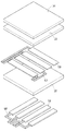
- FIG. 1 and 2 are top views illustrating a fingerprint sensing device according to an embodiment.
- 3 to 8 are cross-sectional views taken along the line AA ′ of FIG. 1.
- FIG. 9 is a diagram illustrating a top view of the fingerprint sensor module according to the embodiment.
- 10 to 15 are cross-sectional views taken along the line AA ′ of FIG. 1.
- 16 is a diagram illustrating another top view of the fingerprint sensor module according to the embodiment.
- 17 to 20 are diagrams for describing various types of touch windows to which a fingerprint sensing device according to an embodiment is applied.
- 21 to 23 are views illustrating a touch device in which a touch window to which a fingerprint sensing device is applied and a display panel are coupled according to an embodiment.
- FIG. 24 is a diagram illustrating an example of a touch device apparatus to which a touch device according to an embodiment is applied.
- each layer, region, pattern, or structure may be “on” or “under” the substrate, each layer, region, pad, or pattern.
- Substrate formed in includes all formed directly or through another layer. Criteria for the top / bottom or bottom / bottom of each layer are described with reference to the drawings.
- each layer (film), region, pattern, or structure may be modified for clarity and convenience of description, and thus do not necessarily reflect the actual size.
- the fingerprint sensing device may include a substrate 100.
- the substrate 100 may be rigid or flexible.
- the substrate 100 may include glass.
- the substrate 100 may include at least one of silicon oxide, aluminum oxide, or sodium oxide.
- the substrate 100 may include chemically strengthened / semi-hardened glass such as soda lime glass or aluminosilicate glass.
- the substrate 100 may be curved while having a partially curved surface. That is, the substrate 100 may be partially curved and partially curved.
- an end of the substrate 100 may have a curved surface, or may have a curved surface or a surface including a random curvature.
- the substrate 100 may be a flexible glass plate having flexible characteristics.
- the substrate 100 may be a curved or bent substrate. That is, the fingerprint sensing device including the substrate 100 may also be formed to have a flexible, curved or bent characteristic. For this reason, the fingerprint sensing device according to the embodiment is easy to carry and can be changed in various designs.
- the thickness T of the substrate 100 may be about 1000 ⁇ m or less.
- the thickness T of the substrate 100 may be defined as a distance from one surface 100a of the substrate 100 to the other surface 100b of the substrate 100, and may be about 1000 ⁇ m or less.
- the thickness T of the substrate 100 may be about 300 ⁇ m to about 1000 ⁇ m.
- an effective area AA and an invalid area UA may be defined in the substrate 100.
- the invalid area UA may be disposed to surround the effective area AA.
- an area of the effective area AA may be larger than that of the ineffective area UA.
- a display may be displayed in the effective area AA, and a display may not be displayed in the non-effective area UA disposed around the effective area AA.
- a plurality of touch sensing electrodes may be disposed on the effective area AA.
- the effective area AA may include a first sensing electrode and a second sensing electrode extending in different directions.
- the first sensing electrode and the second sensing electrode may extend in different directions without being in contact with each other.
- a plurality of wiring electrodes may be disposed on the invalid area UA.
- a first wiring electrode connected to the first sensing electrode and a second wiring electrode connected to the second sensing electrode may be disposed on the non-effective area UA.
- At least one of the effective area AA and the invalid area UA may detect a position of an input device (for example, a finger or a stylus pen).
- an input device for example, a finger or a stylus pen.
- a difference in capacitance occurs in a portion where the input device contacts, and a portion where such a difference occurs may be detected as a contact position.
- the substrate 100 may include a fingerprint sensing area FA.
- the fingerprint sensing area FA may be an area for recognizing a fingerprint.
- An area of the fingerprint sensing area FA may be smaller than an area of the invalid area UA.
- the location of the fingerprint sensing area FA may overlap with the location of the invalid area UA.
- the fingerprint sensing area FA may be located on the invalid area UA.
- the fingerprint sensing area FA may be an area for recognizing a fingerprint of a finger.
- the substrate 100 may be formed in a rectangular shape including a long side and a short side, and the fingerprint sensing area FA may be closer to the short side than the long side.
- an area of the fingerprint sensing area FA may be smaller than that of the substrate 100.
- the area of the fingerprint sensing area FA may be about 0.5% to about 5% of the total area of the substrate.
- grooves may be formed in the fingerprint sensing area FA.
- the substrate 100 may include one surface 100a and the other surface 100b facing the one surface 100a, and the groove may be formed on one surface 100a of the substrate 100. That is, the groove may be formed in an area for recognizing a fingerprint in the substrate 100.
- One surface 100a of the substrate 100 may be a surface on which the fingerprint sensor 200 is disposed.
- the other surface 100b of the substrate 100 may be a surface to which an input device such as a finger contacts.
- an input device such as a finger contacts the other surface 100b of the substrate 100, that is, the other surface 100b of the substrate 100 corresponding to the fingerprint sensing area FA, one surface of the substrate 100 ( An operation according to the contact of the input device may be performed by a fingerprint sensor disposed in the groove formed on the groove 100a.
- the groove may include an inner side surface S and a bottom surface L connecting the inner side surfaces S.
- the substrate 100 may include an inner surface S and a bottom surface L defined by the groove.
- the inner side surface S may extend with an inclination with respect to the bottom surface.
- the distance between the inner surfaces may extend while having an inclination so as to increase while extending from the bottom surface to the one surface 100a of the substrate.
- the groove may have a short width and a long width.
- the short width of the groove may be defined as the inner diameter IR of the groove. That is, the step width of the groove may be defined as the width of the bottom surface (L).
- the long width of the groove may be defined as the outer diameter OR of the groove. That is, the long width of the groove may be defined as the longest width distance of the inner surfaces.
- the contact of the bottom surface (L) and the inner surface (S) and the contact of the inner surface (S) and one surface (100a) of the substrate may be formed at an angle or may be formed in a curved surface.
- the contacts of the bottom surface L and the inner surface S, and the contacts of the inner surface S and the one surface 100a of the substrate may be formed at an angle.
- the contact between the bottom surface L and the inner surface S may be formed in a curved surface, and the contacts between the inner surface S and the one surface 100a of the substrate may have an angle.
- the contact between the bottom surface L and the inner surface S may have an angle, and the contact between the inner surface S and the one surface 100a of the substrate may be formed as a curved surface.
- the contacts of the bottom surface L and the inner surface S and the contacts of the inner surface S and the one surface 100a of the substrate may be formed in a curved surface.
- the fingerprint sensor 210 may be disposed in a groove formed in the substrate 100.
- a first adhesive layer 310 may be disposed in the groove, and the fingerprint sensor 210 may be disposed on the first adhesive layer 310.
- the first adhesive layer 310 may support the fingerprint sensor 210.
- the first adhesive layer 310 may protect the fingerprint sensor 210.
- the first adhesive layer 310 may fix the fingerprint sensor 210.
- the base substrate 220 may be disposed on the fingerprint sensor 210.
- the fingerprint sensor 210 and the base substrate 220 may be connected.
- the fingerprint sensor 210 may include a fingerprint sensing electrode pattern and a fingerprint sensor chip connected to the fingerprint sensing electrode pattern.
- the fingerprint sensor may include a mold part in which a cavity is formed, a fingerprint sensing electrode pattern and a fingerprint sensor chip disposed in the cavity.
- the fingerprint sensor 210 may have a thickness of about 400 ⁇ m to about 600 ⁇ m.
- the base substrate 220 may include polyimide (PI).
- the base substrate 220 may include a printed circuit board.
- the base substrate 210 may include a flexible printed circuit board (FPCB).
- the base substrate 220 may have a thickness of about 20 ⁇ m to about 100 ⁇ m.
- the base substrate 220 may further include an extension part.
- a portion of the base substrate 220 may be disposed in an area corresponding to the groove, and another portion of the base substrate 220 may be disposed outside the fingerprint sensing area.
- the base substrate 220 may extend to an outer region of the groove in order to transmit a signal received from the fingerprint sensor 210.
- the fingerprint sensor 210 and the base substrate 220 may be connected to each other.
- solder paste may be disposed between the fingerprint sensor 210 and the base substrate 220, and the fingerprint sensor 210 and the base substrate 220 may be electrically connected to each other by the solder paste. .
- the first adhesive layer 310 may include a transparent material.
- the first adhesive layer 310 may include a transparent resin material.
- the first adhesive layer 310 may be disposed while filling the inside of the groove. That is, at least one of the fingerprint sensor 210 and the base substrate 220 may be impregnated in the first adhesive layer 310.
- the first adhesive layer 310 may be disposed only inside the groove. Alternatively, the first adhesive layer 310 may be disposed outside the groove. That is, the first adhesive layer may extend on the inside of the groove to be disposed on one surface of the substrate, that is, on one surface of the substrate on which the groove is not formed.
- one surface of the substrate may define a first region 1A in which the groove is formed and a second region 2A other than the first region 1A.
- the first adhesive layer 310 may be disposed only in the first region 1A. Alternatively, the first adhesive layer 310 may be disposed in the first region 1A and the second region 2A.
- the height of the first adhesive layer 310 may be defined as a distance between a contact surface contacting the bottom surface of the groove and a surface opposite to the contact surface.
- the height h2 of the first adhesive layer 310 may be greater than the height h1 of the groove.
- the height h2 of the first adhesive layer 310 may be equal to or less than the height h3 of the upper surface 220a of the base substrate 220. That is, the first adhesive layer 310 may be disposed in contact with at least one side of the side surface 210b of the fingerprint sensor and the side surface 220b of the base substrate. In addition, the first adhesive layer 310 may not be disposed on the upper surface 220a of the base substrate 220.
- the fingerprint sensor 210 and the base substrate 220 can be firmly fixed to the inside of the groove.
- the height h2 of the first adhesive layer 310 may be greater than the height h1 of the groove.
- the height h2 of the first adhesive layer 310 may be equal to or greater than the height h3 of the upper surface 220a of the base substrate 220. That is, the first adhesive layer 310 may be disposed in contact with at least one side of the side surface 210b of the fingerprint sensor and the side surface 220b of the base substrate. In addition, the first adhesive layer 310 may be disposed on the upper surface 220a of the base substrate.
- the fingerprint sensor 210 and the base substrate 220 may be firmly fixed to the inside of the groove, and external impurities that may penetrate into the upper surface of the base substrate may be prevented.
- the first adhesive layer 310 is shown in contact with the front side, but the embodiment is not limited thereto, and the first adhesive layer 310 may be disposed in contact with a portion of the side. .
- the fingerprint sensor 210 and the base substrate 220 may have different sizes.
- the fingerprint sensor 210 and the base substrate 220 may be formed in different widths.
- the width of the base substrate 220 may be larger than the width of the fingerprint sensor 210.
- the width of at least one of the horizontal width W1 and the vertical width W2 of the base substrate 220 may be greater than the width of the fingerprint sensor 210. That is, the width W1 of the base substrate 220 may be greater than the width W3 of the fingerprint sensor 210. Alternatively, the vertical width W2 of the base substrate 220 may be greater than the vertical width W4 of the fingerprint sensor 210. Alternatively, the width and length of the base substrate 220 may be greater than the width and length of the fingerprint sensor 210.
- an area of the base substrate 220 may be larger than that of the fingerprint sensor 210.
- the area of the base substrate 220 may be as large as a predetermined area ratio with respect to the area of the fingerprint sensor 210.
- the area of the base substrate 220 may be about 2 times or less with respect to the size of the area of the fingerprint sensor 210.
- the area ratio of the area of the base substrate 220 and the area of the fingerprint sensor 210 may be about 1.64: 1 to about 2: 1.
- the area ratio of the area of the base substrate 220 to the area of the fingerprint sensor 210 is less than about 1.64: 1, an adhesive material does not sufficiently penetrate the exposed surface of the base substrate and the side of the fingerprint sensor. The adhesion between the base substrate and the fingerprint sensor may be reduced.
- the adhesive force between the base substrate and the fingerprint sensor 210 becomes too strong, thereby applying from the outside. All shocks are transmitted to the fingerprint sensor, which may damage the fingerprint sensor.
- the height h1 of the first adhesive layer 310 may be greater than the height h2 of the groove.
- the height h1 of the first adhesive layer 310 may be equal to or less than the height h3 of the upper surface 220a of the base substrate 220. That is, the first adhesive layer 310 may be disposed in contact with at least one side of the side surface 210b of the fingerprint sensor and the side surface 220b of the base substrate. In addition, the first adhesive layer 310 may not be disposed on the upper surface 220a of the base substrate 220.
- the height h1 of the first adhesive layer 310 may be greater than the height h2 of the groove.
- the height h1 of the first adhesive layer 310 may be equal to or greater than the height h3 of the upper surface 220a of the base substrate 220. That is, the first adhesive layer 310 may be disposed in contact with at least one side of the side surface 210b of the fingerprint sensor and the side surface 220b of the base substrate. In addition, the first adhesive layer 310 may be disposed on the upper surface 220a of the base substrate.
- the first adhesive layer 310 is shown in contact with the front side, but the embodiment is not limited thereto, and the first adhesive layer 310 may be disposed in contact with a portion of the side. .
- a second adhesive layer 320 may be further disposed between the side surface 210b of the fingerprint sensor, the lower surface 220c of the base substrate, and the first adhesive layer 310.
- the second adhesive layer 320 may be in contact with the side surface 210b of the fingerprint sensor and the lower surface 220c of the base substrate.
- the adhesion between the fingerprint sensor 210 and the base substrate 220 may be improved, and the fingerprint sensor 210 may be prevented from being peeled off from the base substrate 220.
- a second adhesive layer 320 may be further disposed between the side surface 210b of the fingerprint sensor, the lower surface 220c of the base substrate, and the first adhesive layer 310. That is, as the width of the base substrate 220 becomes larger than the width of the fingerprint sensor 210, the base substrate 220 and the fingerprint sensor 210 may form a step, and by the step part The side surface 210b of the fingerprint sensor and the lower surface 220c of the base substrate may be exposed. The second adhesive layer 320 may be in contact with the side surface 210b of the fingerprint sensor and the lower surface 220c of the base substrate.
- the adhesion between the fingerprint sensor 210 and the base substrate 220 may be improved, and the fingerprint sensor 210 may be prevented from being peeled off from the base substrate 220.
- the second adhesive layer 320 may include a transparent material.
- the second adhesive layer 320 may include a transparent resin material.
- the first adhesive layer 310 and the second adhesive layer 320 may include the same material.
- the first adhesive layer 310 and the second adhesive layer 320 may be disposed in contact with each other.
- the first adhesive layer 310 and the second adhesive layer 320 may be integrally formed.
- the first adhesive layer 310 and the second adhesive layer 320 may be prevented from peeling off, and moisture or air may pass through the first adhesive layer 310 and the second adhesive layer 320. Penetration can be prevented.
- the first adhesive layer 310 and the second adhesive layer 320 may be formed by different processes. For example, first forming the second adhesive layer 320 on the stepped portion of the base substrate 220 and the fingerprint sensor 210, and then the first adhesive layer 310 is disposed in the groove, The base substrate 220 and the fingerprint sensor 210 may be impregnated in the first adhesive layer 310.
- the first adhesive layer 310 and the second adhesive layer 320 may be formed by the same process.
- the base substrate 220 is disposed by disposing the first adhesive layer 310 inside the groove and impregnating the base substrate 220 and the fingerprint sensor 210 in the first adhesive layer 310.
- the second adhesive layer 320 may be formed on the stepped portion of the fingerprint sensor 210.
- the width of the base substrate 220 may be applied in various sizes depending on the size of the fingerprint sensor to be applied.
- the width of the base substrate 220 may be equal to or less than the long width or less than the short width of the groove.
- the width of the base substrate 220 is greater than the width of the fingerprint sensor 210, and the width of the base substrate 220 is less than or equal to the long width of the groove, that is, less than the outer diameter of the groove.
- the width of the base substrate 220 is greater than the width of the fingerprint sensor 210, and the width of the base substrate 220 is less than or equal to the width of the groove, that is, less than the inner diameter of the groove. May have a size.
- the distance d between the fingerprint sensor 220 and the bottom surface L of the groove may be about 10 ⁇ m to about 40 ⁇ m.
- the first adhesive layer may not be sufficiently disposed between the fingerprint sensor 210 and the bottom surface L.
- the adhesion between the fingerprint sensor and the substrate may be reduced.
- the substrate 100 is in contact with the fingerprint sensor 220 and an input device such as the finger.
- the distance to the other surface 100b of is increased, the sensing sensitivity may be lowered.
- the fingerprint sensing device may further include a display member 350 and a decor layer 400 disposed inside the groove.
- the display member 350 may be disposed on an inner side surface of the groove.
- the display member 350 may be in contact with the inner surface of the groove.
- the display member 350 may include a non-conductive ring-shaped metal.
- the display member 350 may identify a region where the fingerprint sensor 200 is disposed from the outside. That is, the fingerprint sensing area FA may be identified from the outside by the display member 350.
- the decor layer 400 may be disposed on the bottom surface of the groove.
- the decor layer 400 may be disposed in contact with the bottom surface of the groove.
- the fingerprint layer may be prevented from being recognized by the decor layer 400 from the outside.
- FIGS. 10 to 15 a fingerprint sensing device according to another embodiment will be described with reference to FIGS. 10 to 15.
- a description similar to that of the fingerprint sensing device according to the above-described embodiment will be omitted, and the same reference numerals are assigned to the same configuration.
- the fingerprint sensing device may further include a support layer 230 disposed on the base substrate 220.
- the fingerprint sensor 210 in the groove formed in the substrate 100, the fingerprint sensor 210, the base substrate 220 disposed on the fingerprint sensor 210, and the support layer 230 disposed on the base substrate 220. ) Can be inserted.
- the support layer 230 may be disposed on the base substrate 220 exposed to the outside, and serve to protect the base substrate.
- the support layer 230 may include a metal.
- the protective substrate 230 may include stainless steel (SUS).
- the support layer may have a thickness of about 100 ⁇ m to about 200 ⁇ m.
- the support layer 230 on the base substrate 220 may be further included.
- the first adhesive layer 310 may be disposed while filling the inside of the groove. That is, at least one of the fingerprint sensor 210, the base substrate 220, and the support layer 230 may be impregnated in the first adhesive layer 310.
- the first adhesive layer 310 may be disposed only inside the groove. Alternatively, the first adhesive layer 310 may be disposed outside the groove. That is, the first adhesive layer may extend on the inside of the groove to be disposed on one surface of the substrate, that is, on one surface of the substrate on which the groove is not formed.
- one surface of the substrate may define a first region 1A in which the groove is formed and a second region 2A other than the first region 1A.
- the first adhesive layer 310 may be disposed only in the first region 1A. Alternatively, the first adhesive layer 310 may be disposed in the first region 1A and the second region 2A.
- the height of the first adhesive layer 310 may be defined as a distance between a contact surface contacting the bottom surface of the groove and a surface opposite to the contact surface.
- the height h1 of the first adhesive layer 310 may be greater than the height h2 of the groove.
- the height of the first adhesive layer 310 may be equal to or less than the height h4 of the upper surface 230a of the support layer 230. That is, the first adhesive layer 310 may be disposed in contact with at least one side of the side surface 210b of the fingerprint sensor and the side surface 220b of the base substrate. In addition, the first adhesive layer 310 may not be disposed on the upper surface 230a of the support layer.
- the fingerprint sensor 210, the base substrate 220, and the support layer 230 may be firmly fixed to the inside of the groove.
- the height h1 of the first adhesive layer 310 may be greater than the height h2 of the groove.
- the height h1 of the first adhesive layer 310 may be equal to or greater than the height h4 of the upper surface 230a of the support layer. That is, the first adhesive layer 310 may be disposed in contact with at least one side of the side surface 210b of the fingerprint sensor and the side surface 220b of the base substrate. In addition, the first adhesive layer 310 may be disposed on the upper surface 230a of the support layer.
- the fingerprint sensor 210, the base substrate 220, and the support layer 230 may be firmly fixed to the inside of the groove, and external impurities that may penetrate into the upper surface of the support layer may be prevented. can do.
- first adhesive layer 310 is shown in contact with the front side, the embodiment is not limited thereto, and the first adhesive layer 310 may be disposed in contact with a portion of the side surface. .
- the fingerprint sensor 210, the base substrate 220, and the support layer 230 may have different sizes.
- the fingerprint sensor 210, the base substrate 220, and the support layer 230 may have different widths.
- the width of the base substrate 220 and the support layer 230 may be larger than the width of the fingerprint sensor 210.
- Widths of the base substrate 220 and the support layer 230 may correspond to each other. Widths of the base substrate 220 and the support layer 230 may correspond to each other. However, the embodiment is not limited thereto, and the widths of the base substrate 220 and the support layer 230 may be different from each other while being larger than the width of the fingerprint sensor 210.
- the width W1 and the width W2 of the base substrate 220 and the support layer 230 is the size of the width of the fingerprint sensor 210.
- the vertical width W2 of the base substrate 220 and the support layer 230 may be greater than the vertical width W4 of the fingerprint sensor 210.
- the horizontal and vertical widths of the base substrate 220 and the support layer 230 may be greater than the horizontal and vertical widths of the fingerprint sensor 210.
- an area of the base substrate 220 and the support layer 230 may be larger than that of the fingerprint sensor 210.
- An area of the base substrate 220 and the support layer 230 may be as large as a predetermined area ratio with respect to the area of the fingerprint sensor 210.
- the area of the base substrate 220 and the support layer 230 may be about 2 times or less with respect to the size of the area of the fingerprint sensor 210.
- the area ratio of the area of the base substrate 220 and the support layer 230 and the area of the fingerprint sensor 210 may be about 1.64: 1 to about 2: 1.
- the area ratio of the area of the base substrate 220 and the support layer 230 and the area of the fingerprint sensor 210 is less than about 1.64: 1, sufficient adhesive material is provided on the exposed surface of the base substrate and the side of the fingerprint sensor. As it does not penetrate, the adhesion between the base substrate and the fingerprint sensor may be reduced.
- the area ratio of the area of the base substrate 220 and the support layer 230 and the area of the fingerprint sensor 210 exceeds about 2: 1, the adhesion between the base substrate and the fingerprint sensor becomes too strong. Therefore, all shocks applied from the outside are transmitted to the fingerprint sensor, which may damage the fingerprint sensor.
- the height h2 of the first adhesive layer 310 may be greater than the height h1 of the groove.
- the height h2 of the first adhesive layer 310 may be equal to or less than the height h4 of the upper surface 220a of the support layer. That is, the first adhesive layer 310 may be disposed in contact with at least one side of the side surface 210b of the fingerprint sensor and the side surface 220b of the base substrate. In addition, the first adhesive layer 310 may not be disposed on the upper surface 230a of the support layer.
- the height h2 of the first adhesive layer 310 may be greater than the height h1 of the groove.
- the height h2 of the first adhesive layer 310 may be equal to or greater than the height h4 of the upper surface 223a of the support layer. That is, the first adhesive layer 310 may be disposed in contact with at least one side of the side surface 210b of the fingerprint sensor and the side surface 220b of the base substrate. In addition, the first adhesive layer 310 may be disposed on the upper surface 230a of the support layer.
- a second adhesive layer 320 may be further disposed between the side surface 210a of the fingerprint sensor, the lower surface 220b of the base substrate, and the first adhesive layer 310.
- the second adhesive layer 320 may be in contact with the side surface 210a of the fingerprint sensor and the lower surface 220b of the base substrate.
- the first adhesive layer 310 is shown in contact with the front side, but the embodiment is not limited thereto, and the first adhesive layer 310 may be disposed in contact with a portion of the side. .
- the adhesion between the fingerprint sensor 210 and the base substrate 220 may be improved, and the fingerprint sensor 210 may be prevented from being peeled off from the base substrate 220.
- a second adhesive layer 320 may be further disposed between the side surface 210a of the fingerprint sensor, the lower surface 220b of the base substrate, and the first adhesive layer 310. That is, as the width of the base substrate 220 becomes larger than the width of the fingerprint sensor 210, the base substrate 220 and the fingerprint sensor 210 may form a step, and by the step part The side surface 210a of the fingerprint sensor and the lower surface 220b of the base substrate may be exposed. The second adhesive layer 320 may be in contact with the side surface 210a of the fingerprint sensor and the lower surface 220b of the base substrate.
- the adhesion between the fingerprint sensor 210 and the base substrate 220 may be improved, and the fingerprint sensor 210 may be prevented from being peeled off from the base substrate 220.
- the second adhesive layer 320 may include a transparent material.
- the second adhesive layer 320 may include a transparent resin material.
- the first adhesive layer 310 and the second adhesive layer 320 may include the same material.
- the first adhesive layer 310 and the second adhesive layer 320 may be disposed in contact with each other.
- the first adhesive layer 310 and the second adhesive layer 320 may be integrally formed.
- the first adhesive layer 310 and the second adhesive layer 320 may be prevented from peeling off, and moisture or air may pass through the first adhesive layer 310 and the second adhesive layer 320. Penetration can be prevented.
- the first adhesive layer 310 and the second adhesive layer 320 may be formed by different processes. For example, first forming the second adhesive layer 320 on the stepped portion of the base substrate 220 and the fingerprint sensor 210, and then the first adhesive layer 310 is disposed in the groove, The base substrate 220 and the fingerprint sensor 210 may be impregnated in the first adhesive layer 310.
- the first adhesive layer 310 and the second adhesive layer 320 may be formed by the same process.
- the base substrate 220 is disposed by disposing the first adhesive layer 310 inside the groove and impregnating the base substrate 220 and the fingerprint sensor 210 in the first adhesive layer 310.
- the second adhesive layer 320 may be formed on the stepped portion of the fingerprint sensor 210.
- Widths of the base substrate 220 and the support layer 230 may be applied in various sizes depending on the size of the fingerprint sensor to be applied.
- the width of the base substrate 220 and the support layer 230 may be equal to or less than the long width or less than the short width of the groove.
- the width of the base substrate 220 and the support layer 230 is greater than the width of the fingerprint sensor 210, and the width of the base substrate 220 and the support layer 230 is greater than that of the groove. It may have a size less than the long width, that is, less than the outer diameter of the groove.
- the width of the base substrate 220 and the support layer 230 is greater than the width of the fingerprint sensor 210, and the width of the base substrate 220 and the support layer 230 is greater than the width of the base substrate 220 and the support layer 230. It may have a size less than the width of the groove, that is, less than the inner diameter of the groove.
- the distance d between the fingerprint sensor 220 and the bottom surface L of the groove may be about 10 ⁇ m to about 40 ⁇ m.
- the first adhesive layer may not be sufficiently disposed between the fingerprint sensor 210 and the bottom surface L.
- the adhesion between the fingerprint sensor and the substrate may be reduced.
- the substrate 100 is in contact with the fingerprint sensor 220 and an input device such as the finger.
- the distance to the other surface 100b of is increased, the sensing sensitivity may be lowered.
- the fingerprint sensing device may further include a display member 350 and a decor layer 400 disposed in the groove.
- the display member 350 may be disposed on an inner side surface of the groove.
- the display member 350 may be in contact with the inner surface of the groove.
- the display member 350 may include a non-conductive ring-shaped metal.
- the display member 350 may identify a region where the fingerprint sensor 200 is disposed from the outside. That is, the fingerprint sensing area FA may be identified from the outside by the display member 350.
- the decor layer 400 may be disposed on the bottom surface of the groove.
- the decor layer 400 may be disposed in contact with the bottom surface of the groove.
- the fingerprint layer may be prevented from being recognized by the decor layer 400 from the outside.
- the fingerprint sensing device may be arranged to contact the side surfaces of the fingerprint sensor, the base substrate and the support layer, while placing the first adhesive layer fixing the fingerprint sensor, the base substrate and the support layer higher than the height of the groove.
- the fixing force of the fingerprint sensor, the base substrate, and the support layer disposed in the fingerprint sensing region of the substrate may be strengthened.
- the fingerprint sensing device may form the size of the base substrate and / or the support layer disposed on the groove of the fingerprint sensing region formed in the substrate larger than the size of the fingerprint sensor.
- the second adhesive layer may be disposed in the stepped area formed on the base substrate and the fingerprint sensor disposed on the base substrate, and the adhesion between the base substrate and the fingerprint sensor may be improved by the second adhesive layer.
- the fingerprint sensing device may control the ratio of the size of the base substrate and / or the protective layer and the size of the fingerprint sensor at a constant ratio.
- the fingerprint sensing device according to the embodiment may have improved reliability.
- FIGS. 17 to 20 which include the fingerprint sensing device and according to a position where a touch electrode is disposed on the substrate.
- the touch electrodes may be disposed on an effective area of the substrate, and the fingerprint sensing device may be disposed on an invalid area of the substrate.
- the display may be displayed in the effective area, and the display may not be displayed in the invalid area disposed around the valid area.
- the touch window according to the embodiment is disposed on the effective area AA of the substrate 100 and extends in one direction and in a direction different from the one direction. It may include a second sensing electrode 520 extending.
- the unit electrodes of the first sensing electrode 510 may be connected to each other, and the unit electrodes of the second sensing electrode 520 may be spaced apart from each other.
- the second sensing electrodes 520 may include a bridge electrode 530 that connects the unit electrodes to each other.
- the bridge electrodes 530 intersect with an area where the unit electrodes of the first sensing electrode 510 are connected to each other, and an insulating layer is formed between the first sensing electrode 510 and the bridge electrode 530.
- the 530 may be disposed to prevent the first sensing electrode 510 and the second sensing electrode 520 from being electrically connected to each other.
- the first wiring electrode 610 and the second wiring electrode 620 may be disposed on the invalid area UA.
- the first wiring electrode 610 connected to the first sensing electrode 510 and the second wiring electrode 620 connected to the second sensing electrode 520 are disposed in the invalid area UA. Can be arranged.
- a deco layer 400 may be disposed on the ineffective area UA to prevent the wiring electrodes from being visually recognized from the outside.
- another type of touch window includes a substrate 100 and a first substrate 110, and includes a first sensing electrode 510 and the first substrate 110 on the substrate 100. And a second sensing electrode 520 on the top.
- a first sensing electrode 510 extending in one direction and a first wiring electrode 610 connected to the first sensing electrode 510 are disposed on one surface of the substrate 100, and the first substrate (
- a second sensing electrode 520 extending in a direction different from the one direction and a second wiring electrode 620 connected to the second sensing electrode 520 may be disposed on one surface of the 110.
- the sensing electrode may not be disposed on the substrate 100, and the sensing electrode may be disposed only on both surfaces of the first substrate 110.
- a first sensing electrode 510 extending in one direction and a first wiring electrode 610 connected to the first sensing electrode 510 are disposed on one surface of the first substrate 110.
- a second sensing electrode 520 extending in a direction different from the one direction and a second wiring electrode 620 connected to the second sensing electrode 520 may be disposed on the other surface of the substrate 110.
- a touch window according to another type includes a substrate 100, a first substrate 110, and a second substrate 120, and a first sensing electrode 510 on the first substrate 110. ) And a second sensing electrode 520 on the second substrate 120.
- a first sensing electrode 510 extending in one direction and a first wiring electrode 610 connected to the first sensing electrode 510 are disposed on one surface of the first substrate 110.
- a second sensing electrode 520 extending in a direction different from the one direction and a second wiring electrode 620 connected to the second sensing electrode 520 may be disposed on one surface of the substrate 120.
- a touch window according to another type may include a substrate 100, a first sensing electrode 510, and a second sensing electrode 520 on the substrate.
- the first sensing electrode 510 and the second sensing electrode 520 may be disposed on the same surface of the substrate 100.
- the first sensing electrode 510 and the second sensing electrode 520 may be spaced apart from each other on the same surface of the substrate 100.
- a first wiring electrode 610 connected to the first sensing electrode 510 and a second wiring electrode 620 connected to the second sensing electrode 520 may be included, and the first wiring electrode ( 610 may be disposed on the effective area and the invalid area of the substrate 100, and the second wiring electrode 620 may be disposed on the invalid area of the substrate 100.
- the touch window described above may be applied to a touch device in combination with a display panel.
- the touch window may be coupled to the display panel by an adhesive layer.
- the touch device may include a touch window disposed on the display panel 800.
- the touch device may be formed by combining the substrate 100 and the display panel 800.
- the substrate 100 and the display panel 800 may be adhered to each other through an adhesive layer 700.
- the substrate 100 and the display panel 800 may be laminated to each other through an adhesive layer 700 including optically clear adhesives OCA and OCR.
- the display panel 800 may include a first 'substrate 810 and a second' substrate 820.
- the display panel 800 When the display panel 800 is a liquid crystal display panel, the display panel 800 includes a first 'substrate 810 including a thin film transistor (TFT) and a pixel electrode and a second filter including color filter layers.
- the substrate 820 may be formed in a bonded structure with the liquid crystal layer interposed therebetween.
- the display panel 800 includes a thin film transistor, a color filter, and a black matrix formed on the first 'substrate 810, and the second' substrate 820 has the liquid crystal layer interposed therebetween.
- a liquid crystal display panel having a color filter on transistor (COT) structure That is, a thin film transistor may be formed on the first 'substrate 810, a protective film may be formed on the thin film transistor, and a color filter layer may be formed on the protective film.
- a pixel electrode in contact with the thin film transistor is formed on the first 'substrate 810.
- the black matrix may be omitted in order to improve the aperture ratio and simplify the mask process, and the common electrode may be formed to serve as the black matrix.
- the display device may further include a backlight unit that provides light from the back of the display panel 800.
- the display panel 800 When the display panel 800 is an organic light emitting display panel, the display panel 800 includes a self-light emitting device that does not require a separate light source.
- a thin film transistor is formed on the first ′ substrate 910, and an organic light emitting diode is formed in contact with the thin film transistor.
- the organic light emitting diode may include an anode, a cathode, and an organic light emitting layer formed between the anode and the cathode.
- the organic light emitting device may further include a second 'substrate 820 serving as an encapsulation substrate for encapsulation.
- the touch device may include a touch window integrally formed with the display panel 800. That is, the substrate supporting at least one sensing electrode may be omitted.
- At least one sensing electrode may be disposed on at least one surface of the display panel 800. That is, at least one sensing electrode may be formed on at least one surface of the first 'substrate 810 or the second' substrate 820.
- At least one sensing electrode may be formed on the upper surface of the substrate disposed above.
- a first sensing electrode 510 may be disposed on one surface of the substrate 100.
- a first wire connected to the first sensing electrode 510 may be disposed.
- a second sensing electrode 520 may be disposed on one surface of the display panel 800.
- a second wiring connected to the second sensing electrode 520 may be disposed.
- An adhesive layer 700 may be disposed between the substrate 100 and the display panel 800 so that the substrate and the display panel 800 are laminated to each other.
- a polarizer may be further included below the substrate 100.
- the polarizing plate may be a linear polarizing plate or an external light reflection preventing polarizing plate.
- the polarizer may be a linear polarizer.
- the polarizing plate may be an anti-reflection polarizing plate.
- the touch device according to the embodiment may omit at least one substrate supporting the sensing electrode. For this reason, a thin and light touch device can be formed.
- the touch device may include a touch window integrally formed with the display panel 900. That is, the substrate supporting at least one sensing electrode may be omitted.
- a sensing electrode disposed in an effective area and serving as a sensor for sensing a touch and a wiring for applying an electrical signal to the sensing electrode may be formed inside the display panel.
- at least one sensing electrode or at least one wiring may be formed inside the display panel.
- the display panel includes a first 'substrate 810 and a second' substrate 820.
- at least one sensing electrode of the first sensing electrode 510 and the second sensing electrode 520 is disposed between the first 'substrate 810 and the second' substrate 820. That is, at least one sensing electrode may be disposed on at least one surface of the first 'substrate 810 or the second' substrate 820.
- a first sensing electrode 510 may be disposed on one surface of the substrate 100.
- a first wire connected to the first sensing electrode 510 may be disposed.
- a second sensing electrode 520 and a second wiring may be formed between the first 'substrate 810 and the second' substrate 820. That is, the second sensing electrode 520 and the second wiring may be disposed inside the display panel, and the first sensing electrode 510 and the first wiring may be disposed outside the display panel.
- the second sensing electrode 520 and the second wiring may be disposed on an upper surface of the first 'substrate 810 or a rear surface of the second' substrate 820.
- a polarizer may be further included below the substrate 100.
- the sensing electrode when the display panel is a liquid crystal display panel, when the second sensing electrode is formed on the upper surface of the first 'substrate 810, the sensing electrode may be formed with a thin film transistor (TFT) or a pixel electrode. have.
- TFT thin film transistor
- a color filter layer may be formed on the sensing electrode, or a sensing electrode may be formed on the color filter layer.
- the display panel is an organic light emitting display panel
- the second sensing electrode 520 when the second sensing electrode 520 is formed on an upper surface of the first 'substrate 810, the second sensing electrode is formed together with a thin film transistor or an organic light emitting diode. Can be.
- the touch device according to the embodiment may omit at least one substrate supporting the sensing electrode. For this reason, a thin and light touch device can be formed.
- the sensing electrode and the wiring may be formed together with the elements formed on the display panel to simplify the process and reduce the cost.
- a mobile terminal is shown as an example of a touch device apparatus.
- the mobile terminal may include an effective area AA and an invalid area UA.
- the effective area AA may detect a touch signal by a touch of a finger or the like, and a command icon pattern part and a logo may be formed in the invalid area.
Abstract
실시예에 따른 지문센싱 장치는, 기판; 상기 기판의 지문을 인식하기 위한 영역에 형성되는 홈; 상기 홈의 내부에 배치되는 제 1 접착층; 상기 제 1 접착층 상에 배치되는 지문센서; 상기 지문센서 상에 배치되는 베이스기판; 및 상기 베이스 기판 상에 배치되는 지지층을 포함하고, 상기 베이스 기판의 폭은 상기 지문센서 모듈의 폭보다 크고, 상기 제 1 접착층은 상기 홈의 높이보다 크고 상기 지지층의 상면 높이 이하인 높이로 배치된다.
Description
실시예는 지문센싱 장치 및 이를 포함하는 터치 디바이스에 대한 것이다.
지문센서는 사람의 지문을 감지하는 센서로서, 기존에 널리 적용되던 도어락 등의 장치는 물론, 최근에는 전자 기기 전원의 온/오프 또는 슬립(sleep) 모드의 해제 여부를 결정하는 데에도 널리 이용되고 있다.
이러한 지문 센서가 터치 윈도우에 적용되는 경우, 지문센서 커버의 일면 상에 지문센서가 배치될 수 있다.
그러나, 상기 지문센서의 배치로 인해, 지문센서 커버의 전체적인 두께가 저하되는 문제점이 있다.
이러한 문제점을 해결하기 위해, 지문센서커버의 일 영역에 수용부를 형성하고, 상기 수용부에 지문센서 모듈을 삽입할 수 있다.
그러나, 상기 수용부 내부에 형성되는 상기 지문센서 모듈이 외부의 충격 등에 의해 손상되어 신뢰성이 저하되는 문제점이 있다.
따라서, 이와 같은 문제점을 해결할 수 있는 새로운 구조의 지문센싱 장치가 요구된다.
실시예는 향상된 신뢰성을 가지는 지문센싱 장치를 제공하고자 한다.
실시예에 따른 지문센싱 장치는, 기판; 상기 기판의 지문을 인식하기 위한 영역에 형성되는 홈; 상기 홈의 내부에 배치되는 제 1 접착층; 상기 제 1 접착층 상에 배치되는 지문센서; 상기 지문센서 상에 배치되는 베이스기판; 및 상기 베이스 기판 상에 배치되는 지지층을 포함하고, 상기 베이스 기판의 폭은 상기 지문센서 모듈의 폭보다 크고, 상기 제 1 접착층은 상기 홈의 높이보다 크고 상기 지지층의 상면 높이 이하인 높이로 배치된다.
실시예에 따른 지문센싱 장치는 지문센서, 베이스 기판 및 지지층을 고정하는 제 1 접착층을 홈의 높이보다 높게 배치하면서, 상기 지문센서, 베이스 기판 및 지지층의 측면과 접촉하도록 배치할 수 있다.
이에 따라, 상기 기판의 지문센싱영역에 배치되는 상기 지문센서, 베이스 기판 및 지지층의 고정력을 강화시킬 수 있다.
또한, 실시예에 따른 지문센싱 장치는 기판에 형성된 지문센싱영역의 홈 상에 배치되는 베이스 기판 및/또는 지지층의 크기를 지문센서의 크기보다 크게 형성할 수 있다.
이에 따라, 상기 베이스 기판과 상기 베이스 기판 상에 배치되는 지문센서 에 형성되는 단차 영역에 제 2 접착층을 배치할 수 있고, 상기 제 2 접착층에 의해 상기 베이스 기판과 상기 지문센서의 접착력을 향상시킬 수 있다.
또한, 실시예에 따른 지문센싱 장치는 상기 베이스 기판 및/또는 상기 보호층의 크기와 상기 지문센서 칩의 크기의 비를 일정한 비율로 제어할 수 있다.
이에 따라, 외부에서 가해지는 충격이 지문센서 칩에 집중되어 지문센서가 손상되는 것을 방지할 수 있다.
따라서, 실시예에 따른 지문센싱 장치는 향상된 신뢰성을 가질 수 있다.
도 1 및 도 2는 실시예에 따른 지문센싱 장치의 상면도를 도시한 도면들이다.
도 3 내지 도 8은 도 1의 A-A' 영역을 절단하여 도시한 단면도를 도시한 도면들이다.
도 9는 실시예에 따른 지문센서 모듈의 상면도를 도시한 도면이다.
도 10 내지 15는 도 1의 A-A' 영역을 절단하여 도시한 다른 단면도를 도시한 도면들이다.
도 16은 실시예에 따른 지문센서 모듈의 다른 상면도를 도시한 도면이다.
도 17 내지 도 20은 실시예에 따른 지문센싱 장치가 적용되는 터치 윈도우의 다양한 타입을 설명하기 위한 도면들이다.
도 21 내지 도 23은 실시예에 따른 지문센싱 장치가 적용되는 터치 윈도우와 표시 패널이 결합되는 터치 디바이스를 도시한 도면들이다.
도 24는 실시예에 따른 터치 디바이스가 적용되는 터치 디바이스 장치의 일례를 도시한 도면들이다.
실시예들의 설명에 있어서, 각 층(막), 영역, 패턴 또는 구조물들이 기판, 각 층(막), 영역, 패드 또는 패턴들의 “상/위(on)”에 또는 “하/아래(under)”에 형성된다는 기재는, 직접(directly) 또는 다른 층을 개재하여 형성되는 것을 모두 포함한다. 각 층의 상/위 또는 하/아래에 대한 기준은 도면을 기준으로 설명한다.
또한, 어떤 부분이 다른 부분과 "연결"되어 있다고 할 때, 이는 "직접적으로 연결"되어 있는 경우뿐아니라, 그 중간에 다른 부재를 사이에 두고 "간접적으로 연결"되어 있는 경우도 포함한다. 또한 어떤 부분이어떤 구성요소를 "포함"한다고 할 때, 이는 특별히 반대되는 기재가 없는 한 다른 구성요소를 제외하는 것이 아니라 다른 구성요소를 더 구비할 수 있다는 것을 의미한다.
도면에서 각 층(막), 영역, 패턴 또는 구조물들의 두께나 크기는 설명의 명확성 및 편의를 위하여 변형될 수 있으므로, 실제 크기를 전적으로 반영하는 것은 아니다.
이하, 도면들을 참조하여, 실시예에 따른 지문센싱 장치를 설명한다.
도 1 및 도 2를 참조하면, 실시예에 따른 지문센싱 장치는 기판(100)을 포함할 수 있다.
상기 기판(100)은 리지드하거나 플렉서블할 수 있다. 예를 들어, 상기 기판(100)은 유리를 포함할 수 있다. 자세하게, 상기 기판(100)은 규소산화물, 알루미늄산화물 또는 나트륨산화물 중 적어도 하나를 포함할 수 있다. 일례로, 상기 기판(100)은 소다라임유리(soda lime glass) 또는 알루미노실리케이트유리 등의 화학 강화/반강화유리를 포함할 수 있다.
또한, 상기 기판(100)은 부분적으로 곡면을 가지면서 휘어질 수 있다. 즉, 상기 기판(100)은 부분적으로는 평면을 가지고, 부분적으로는 곡면을 가지면서 휘어질 수 있다. 자세하게, 상기 기판(100)의 끝단이 곡면을 가지면서 휘어지거나 랜덤한 곡률을 포함한 표면을 가지며 휘어지거나 구부러질 수 있다.
또한, 상기 기판(100)은 유연한 특성을 가지는 플렉서블(flexible) 유리판일 수 있다.
또한, 상기 기판(100)은 커브드(curved) 또는 벤디드(bended) 기판일 수 있다. 즉, 상기 기판(100)을 포함하는 지문센싱 장치도 플렉서블, 커브드 또는 벤디드 특성을 가지도록 형성될 수 있다. 이로 인해, 실시예에 따른 지문센싱 장치는 휴대가 용이하며, 다양한 디자인으로 변경이 가능할 수 있다.
상기 기판(100)의 두께(T)는 약 1000㎛ 이하일 수 있다. 자세하게, 상기 기판(100)의 두께(T)는 상기 기판(100)의 일면(100a)에서 상기 기판(100)의 타면(100b)까지의 거리로 정의될 수 있고, 약 1000㎛이하 일 수 있다. 자세하게, 상기 기판(100)의 두께(T)는 약 300㎛ 내지 약 1000㎛일 수 있다.
도 2를 참조하면, 상기 기판(100)에는 유효 영역(AA) 및 비유효 영역(UA)이 정의될 수 있다.
상기 비유효 영역(UA)은 상기 유효 영역(AA)을 둘러싸며 배치될 수 있다. 또한, 상기 유효 영역(AA)의 면적은 상기 비유효 영역(UA)의 면적보다 클 수 있다.
상기 유효 영역(AA)에서는 디스플레이가 표시될 수 있고, 상기 유효 영역(AA) 주위에 배치되는 상기 비유효 영역(UA)에서는 디스플레이가 표시되지 않을 수 있다.
예를 들어, 상기 유효 영역(AA) 상에는 복수 개의 터치 감지 전극들이 배치될 수 있다. 자세하게, 상기 유효 영역(AA) 상에는 서로 다른 방향으로 연장하는제 1 감지 전극 및 제 2 감지 전극을 포함할 수 있다. 상기 제 1 감지 전극 및 상기 제 2 감지 전극은 서로 접촉되지 않으면서, 서로 다른 방향으로 연장되며 배치될 수 있다.
또한, 상기 비유효 영역(UA) 상에는 복수 개의 배선 전극들이 배치될 수 있다. 자세하게, 상기 비유효 영역(UA) 상에는 상기 제 1 감지 전극과 연결되는 제 1 배선 전극 및 상기 제 2 감지 전극과 연결되는 제 2 배선 전극이 배치될 수 있다.
또한, 상기 유효 영역(AA) 및 상기 비유효 영역(UA) 중 적어도 하나의 영역에서는 입력 장치(예를 들어, 손가락 또는 스타일러스 펜 등)의 위치를 감지할 수 있다. 자세하게, 상기 유리판(100) 상에 손가락 등의 입력 장치가 접촉되면, 입력 장치가 접촉된 부분에서 정전 용량의 차이가 발생하고, 이러한 차이가 발생한 부분을 접촉 위치로 검출할 수 있다.
상기 기판(100)은 지문센싱영역(FA)을 포함할 수 있다. 상기 지문센싱영역(FA)은 지문을 인식하기 위한 영역일 수 있다. 상기 지문센싱영역(FA)의 면적은 상기 비유효 영역(UA)의 면적보다 작을 수 있다. 상기 지문센싱영역(FA)의 위치는 상기 비유효 영역(UA)의 위치와 중첩될 수 있다. 자세하게, 상기 지문센싱영역(FA)은 상기 비유효 영역(UA) 상에 위치될 수 있다.
상기 지문센싱영역(FA)은 손가락의 지문 등을 인식하는 영역일 수 있다.
또한, 상기 기판(100)은 장변 및 단변을 포함하는 사각형 형상으로 형성될 수 있고, 상기 지문센싱영역(FA)은 상기 장변보다 상기 단변에 가까울 수 있다.
또한, 상기 지문센싱영역(FA)의 면적은 상기 기판(100)의 면적보다 작을 수 있다. 자세하게, 상기 지문센싱영역(FA)의 면적은 상기기판 전체 면적에 대해 약 0.5% 내지 약 5% 크기를 가질 수 있다.
도 3 내지 도 6을 참조하면, 상기 지문센싱영역(FA)에는 홈이 형성될 수 있다. 자세하게, 상기 기판(100)은 일면(100a) 및 상기 일면(100a)과 마주보는 타면(100b)을 포함하고, 상기 기판(100)의 일면(100a)에는 상기 홈이 형성될 수 있다. 즉, 상기 홈은 상기 기판(100)에서 지문을 인식하기 위한 영역에 형성될 수 있다.
상기 기판(100)의 일면(100a)은 지문센서(200)가 배치되는 면일 수 있다. 또한, 상기 기판(100)의 타면(100b)은 손가락 등의 입력 장치가 접촉되는 면일 수 있다.
상기 기판(100)의 타면(100b) 즉, 상기 지문센싱영역(FA)과 대응되는 상기 기판(100)의 타면(100b)에 손가락 등의 입력 장치가 접촉되면, 상기 기판(100)의 일면(100a) 상에 형성되는 홈 내부에 배치되는 지문센서 등에 의해 입력 장치의 접촉에 따른 동작이 수행될 수 있다.
상기 홈은 내측면(S) 및 상기 내측면(S)들을 연결하는 바닥면(L)을 포함할 수 있다. 즉, 상기 기판(100)은 상기 홈에 의해 정의되는 내측면(S) 및 바닥면(L)을 포함할 수 있다.
상기 내측면(S)은 상기 바닥면에 대해 경사를 가지면서 연장될 수 있다. 예를 들어, 상기 내측면들의 거리는 상기 바닥면으로부터 상기 기판의 일면(100a)으로 연장하면서 커지도록 경사를 가지면서 연장될 수 있다.
이에 따라, 상기 홈은 단폭 및 장폭을 가질 수 있다.
자세하게, 상기 홈의 단폭은 상기 홈의 내경(IR)으로 정의될 수 있다. 즉, 상기 홈의 단폭은 상기 바닥면(L)의 폭으로 정의될 수 있다
또한, 상기 홈의 장폭은 상기 홈의 외경(OR)으로 정의될 수 있다. 즉, 상기 홈의 장폭은 상기 내측면들의 최장폭 거리로 정의될 수 있다.
상기 바닥면(L)과 상기 내측면(S)의 접점 및 상기 내측면(S) 및 상기 기판의 일면(100a)의 접점은 각을 지면서 형성되거나 또는 곡면으로 형성될 수 있다.
예를 들어, 또는, 상기 바닥면(L)과 상기 내측면(S)의 접점과, 상기 내측면(S) 및 상기 기판의 일면(100a)의 접점은 모두 각을 가지며 형성될 수 있다.
또는, 상기 바닥면(L)과 상기 내측면(S)의 접점은 곡면으로 형성되고, 상기 내측면(S) 및 상기 기판의 일면(100a)의 접점은 각을 가지며 형성될 수 있다.
또는, 상기 바닥면(L)과 상기 내측면(S)의 접점은 각을 가지며 형성되고, 상기 내측면(S) 및 상기 기판의 일면(100a)의 접점은 곡면으로 형성될 수 있다.
또는, 상기 바닥면(L)과 상기 내측면(S)의 접점과, 상기 내측면(S) 및 상기 기판의 일면(100a)의 접점은 모두 곡면으로 형성될 수 있다.
도 3 및 도 4를 참조하면, 상기 지문센서(210)는 상기 기판(100)에 형성되는 홈의 내부에 배치될 수 있다. 예를 들어, 상기 홈의 내부에는 제 1 접착층(310)이 배치되고, 상기 지문센서(210)는 상기 제 1 접착층(310) 상에 배치될 수 있다. 상기 제 1 접착층(310)은 상기 지문센서(210)를 지지할 수 있다. 상기 제 1 접착층(310)은 상기 지문센서(210)를 보호할 수 있다. 상기 제 1 접착층(310)은 상기 지문센서(210)를 고정할 수 있다.
상기 지문센서(210) 상에는 베이스 기판(220)이 배치될 수 있다. 상기 지문센서(210)와 상기 베이스 기판(220)은 연결될 수 있다.
상기 지문센서(210)는 지문센싱전극 패턴 및 상기 지문센싱 전극 패턴과 연결되는 지문센서 칩을 포함할 수 있다. 예를 들어, 상기 지문센서는 캐비티가 형성된 몰드부 및 상기 캐비티 내에 배치되는 지문센싱전극 패턴 및 지문센서 칩을 포함할 수 있다.
상기 지문센서(210)의 두께는 약 400㎛ 내지 약 600㎛일 수 있다.
상기 베이스 기판(220)은 폴리이미드(PI)를 포함할 수 있다. 상기 베이스 기판(220)은 인쇄회로기판을 포함할 수 있다. 상기 베이스 기판(210)은 플렉서블 인쇄회로기판(FPCB)을 포함할 수 있다.
상기 베이스 기판(220)의 두께는 약 20㎛ 내지 약 100㎛일 수 있다.
상기 베이스 기판(220)은 연장부를 더 포함할수도 있다. 예를 들어, 상기 베이스 기판(220)의 일부분은 홈과 대응되는 영역에 배치되고, 다른 일부분은 지문센싱영역 바깥쪽에 배치될 수 있다. 이때, 상기 베이스 기판(220)은 상기 지문센서(210)로부터 전달받은 신호를 전달하기 위하여 홈의 바깥 영역으로 연장될 수 있다.
상기 지문센서(210)와 상기 베이스 기판(220)은 서로 연결될 수 있다. 예를 들어, 상기 지문센서(210)와 상기 베이스 기판(220) 사이에는 솔더 페이스트가 배치되고, 상기 솔더 페이스트에 의해 상기 지문센서(210)와 상기 베이스 기판(220)은 서로 전기적으로 연결될 수 있다.
상기 제 1 접착층(310)은 투명한 물질을 포함할 수 있다. 예를 들어, 상기 제 1 접착층(310)은 투명한 수지(resin) 물질을 포함할 수 있다.
상기 제 1 접착층(310)은 상기 홈의 내부를 메우면서 배치될 수 있다. 즉, 상기 지문센서(210) 및 상기 베이스 기판(220) 중 적어도 하나는 상기 제 1 접착층(310)에 함침될 수 있다.
상기 제 1 접착층(310)은 상기 홈의 내부에만 배치될 수 있다. 또는, 상기 제 1 접착층(310)은 상기 홈의 외부에도 배치될 수 있다. 즉, 상기 제 1 접착층은 상기 홈의 내부에서 연장되어 상기 기판의 일면 즉, 상기 홈이 형성되지 않은 상기 기판의 일면 상에도 배치될 수 있다.
예를 들어, 상기 기판의 일면은 상기 홈이 형성되는 제 1 영역(1A) 및 상기 제 1 영역(1A) 이외의 제 2 영역(2A)이 정의될 수 있다.
상기 제 1 접착층(310)은 상기 제 1 영역(1A)에만 배치될 수 있다. 또는, 상기 제 1 접착층(310)은 상기 제 1 영역(1A) 및 상기 제 2 영역(2A)에 배치될 수 있다.
상기 제 1 접착층(310)의 높이는 상기 홈의 바닥면과 접촉하는 접촉면 및 상기 접촉면과 반대되는 면의 거리로 정의될 수 있다.
도 3을 참조하면, 상기 제 1 접착층(310)의 높이(h2)는 상기 홈의 높이(h1)보다 클 수 있다. 또한, 상기 제 1 접착층(310)의 높이(h2)는 상기 베이스 기판(220)의 상부면(220a)의 높이(h3) 이하일 수 있다. 즉, 상기 제 1 접착층(310)은 상기 지문센서의 측면(210b) 및 상기 베이스 기판의 측면(220b) 중 적어도 하나의 측면과 접촉하며 배치될 수 있다. 또한, 상기 제 1 접착층(310)은 상기 베이스 기판(220)의 상부면(220a) 상에는 배치되지 않을 수 있다.
이에 따라, 상기 지문센서(210) 및 상기 베이스 기판(220)을 상기 홈의 내부에 견고하게 고정할 수 있다.
또는, 도 4를 참조하면, 상기 제 1 접착층(310)의 높이(h2)는 상기 홈의 높이(h1)보다 클 수 있다. 또한, 상기 제 1 접착층(310)의 높이(h2)는 상기 베이스 기판(220)의 상부면(220a)의 높이(h3) 이상일 수 있다. 즉, 상기 제 1 접착층(310)은 상기 지문센서의 측면(210b) 및 상기 베이스 기판의 측면(220b) 중 적어도 하나의 측면과 접촉하며 배치될 수 있다. 또한, 상기 제 1 접착층(310)은 상기 베이스 기판의 상부면(220a) 상에도 배치될 수 있다.
이에 따라, 상기 지문센서(210) 및 상기 베이스 기판(220)을 상기 홈의 내부에 견고하게 고정할 수 있고, 상기 베이스 기판의 상면으로 침투될 수 있는 외부의 불순물 등을 방지할 수 있다.
도 3 및 도 4에서는, 상기 제 1 접착층(310)이 전 측면과 접촉하는 것으로 도시되었으나, 실시예는 이에 제한되지 않고, 상기 제 1 접착층(310)은 측면의 일부분과 접촉하며 배치될 수도 있다.
도 5 및 도 6을 참조하면, 상기 지문센서(210)와 상기 베이스 기판(220)은 서로 다른 크기를 가질 수 있다. 자세하게, 상기 지문센서(210)와 상기 베이스 기판(220)은 서로 다른 폭으로 형성될 수 있다. 더 자세하게, 상기 베이스 기판(220)의 폭은 상기 지문센서(210)의 폭보다 클 수 있다.
예를 들어, 도 9를 참조하면, 상기 베이스 기판(220)의 가로 폭(W1) 및 세로 폭(W2) 중 적어도 하나의 폭은 상기 지문센서(210)의 폭의 크기보다 클 수 있다. 즉, 상기 베이스 기판(220)의 가로 폭(W1)은 상기 지문센서(210)의 가로 폭(W3)보다 클 수 있다. 또는, 상기 베이스 기판(220)의 세로 폭(W2)은 상기 지문센서(210)의 세로 폭(W4)보다 클 수 있다. 또는, 상기 베이스 기판(220)의 가로 및 세로 폭은 상기 지문센서(210)의 가로 및 세로 폭보다 클 수 있다.
또는, 상기 베이스 기판(220)의 면적은 상기 지문센서(210)의 면적보다 클 수 있다.
상기 베이스 기판(220)의 면적은 상기 지문센서(210)의 면적에 대해 일정한 면적비 만큼 클 수 있다.
자세하게, 상기 베이스 기판(220)의 면적은 상기 지문센서(210)의 면적의 크기에 대해 약 2배 이하일 수 있다.
더 자세하게, 상기 베이스 기판(220)의 면적과 상기 지문센서(210)의 면적의 면적비는 약 1.64:1 내지 약 2:1일 수 있다.
상기 베이스 기판(220)의 면적과 상기 지문센서(210)의 면적의 면적비가 약 1.64:1 미만인 경우, 상기 베이스 기판의 노출면과 상기 지문센서의 측면에 접착 물질이 충분하게 침투되지 않아, 상기 베이스 기판과 상기 지문센서의 접착력이 저하될 수 있다.
또한, 상기 베이스 기판(220)의 면적과 상기 지문센서(210)의 면적의 면적비가 약 2:1을 초과하는 경우, 상기 베이스 기판과 상기 지문센서의 접착력이 너무 강해지고, 이에 따라 외부에서 인가되는 충격이 모두 지문센서로 전달되어 지문센서가 손상될 수 있다.
도 5를 참조하면, 상기 제 1 접착층(310)의 높이(h1)는 상기 홈의 높이(h2)보다 클 수 있다. 또한, 상기 제 1 접착층(310)의 높이(h1)는 상기 베이스 기판(220)의 상부면(220a)의 높이(h3) 이하일 수 있다. 즉, 상기 제 1 접착층(310)은 상기 지문센서의 측면(210b) 및 상기 베이스 기판의 측면(220b) 중 적어도 하나의 측면과 접촉하며 배치될 수 있다. 또한, 상기 제 1 접착층(310)은 상기 베이스 기판(220)의 상부면(220a) 상에는 배치되지 않을 수 있다.
또는, 도 6을 참조하면, 상기 제 1 접착층(310)의 높이(h1)는 상기 홈의 높이(h2)보다 클 수 있다. 또한, 상기 제 1 접착층(310)의 높이(h1)는 상기 베이스 기판(220)의 상부면(220a)의 높이(h3) 이상일 수 있다. 즉, 상기 제 1 접착층(310)은 상기 지문센서의 측면(210b) 및 상기 베이스 기판의 측면(220b) 중 적어도 하나의 측면과 접촉하며 배치될 수 있다. 또한, 상기 제 1 접착층(310)은 상기 베이스 기판의 상부면(220a) 상에도 배치될 수 있다.
도 5 및 도 6에서는, 상기 제 1 접착층(310)이 전 측면과 접촉하는 것으로 도시되었으나, 실시예는 이에 제한되지 않고, 상기 제 1 접착층(310)은 측면의 일부분과 접촉하며 배치될 수도 있다.
또한, 도 5 및 도 6을 참조하면, 상기 지문센서의 측면(210b), 상기 베이스 기판의 하부면(220c) 및 상기 제 1 접착층(310)의 사이에는 제 2 접착층(320)이 더 배치될 수 있다. 즉, 상기 베이스 기판(220)의 폭이 상기 지문센서(210)의 폭보다 크게 됨에 따라, 상기 베이스 기판(220)과 상기 지문센서(210)는 단차를 형성할 수 있고, 상기 단차부에 의해 상기 지문센서의 측면(210b)과 상기 베이스 기판의 하부면(220c)이 노출될 수 있다. 상기 제 2 접착층(320)은 상기 지문센서의 측면(210b)과 상기 베이스 기판의 하부면(220c)과 접촉하며 배치될 수 있다.
이에 따라, 상기 지문센서(210)와 상기 베이스 기판(220)의 접착력이 향상될 수 있고, 상기 지문센서(210)가 상기 베이스 기판(220)으로부터 박리되는 것을 방지할 수 있다.
또한, 상기 지문센서의 측면(210b), 상기 베이스 기판의 하부면(220c) 및 상기 제 1 접착층(310)의 사이에는 제 2 접착층(320)이 더 배치될 수 있다. 즉, 상기 베이스 기판(220)의 폭이 상기 지문센서(210)의 폭보다 크게 됨에 따라, 상기 베이스 기판(220)과 상기 지문센서(210)는 단차를 형성할 수 있고, 상기 단차부에 의해 상기 지문센서의 측면(210b)과 상기 베이스 기판의 하부면(220c)이 노출될 수 있다. 상기 제 2 접착층(320)은 상기 지문센서의 측면(210b)과 상기 베이스 기판의 하부면(220c)과 접촉하며 배치될 수 있다.
이에 따라, 상기 지문센서(210)와 상기 베이스 기판(220)의 접착력이 향상될 수 있고, 상기 지문센서(210)가 상기 베이스 기판(220)으로부터 박리되는 것을 방지할 수 있다.
상기 제 2 접착층(320)은 투명한 물질을 포함할 수 있다. 예를 들어, 상기 제 2 접착층(320)은 투명한 수지(resin) 물질을 포함할 수 있다.
상기 제 1 접착층(310)과 상기 제 2 접착층(320)은 동일한 물질을 포함할 수 있다. 상기 제 1 접착층(310)과 상기 제 2 접착층(320)은 서로 접촉되며 배치될 수 있다. 상기 제 1 접착층(310)과 상기 제 2 접착층(320)은 일체로 형성될 수 있다.
이에 따라, 상기 제 1 접착층(310)과 상기 제 2 접착층(320)이 박리되는 것을 방지할 수 있고, 상기 제 1 접착층(310) 및 상기 제 2 접착층(320) 사이를 통해 수분 또는 공기 등이 침투되는 것을 방지할 수 있다.
상기 제 1 접착층(310)과 상기 제 2 접착층(320)은 서로 다른 공정으로 형성될 수 있다. 예를 들어, 상기 베이스 기판(220)과 상기 지문센서(210)의 단차부에 먼저 상기 제 2 접착층(320)을 형성한 후, 상기 제 1 접착층(310)을 상기 홈의 내부에 배치하고, 상기 베이스 기판(220)과 상기 지문센서(210)를 상기 제 1 접착층(310)에 함침시킬 수 있다.
또는, 상기 제 1 접착층(310)과 상기 제 2 접착층(320)은 서로 동일한 공정으로 형성될 수 있다. 예를 들어, 상기 제 1 접착층(310)을 상기 홈의 내부에 배치하고, 상기 베이스 기판(220)과 상기 지문센서(210)를 상기 제 1 접착층(310)에 함침시킴으로써, 상기 베이스 기판(220)과 상기 지문센서(210)의 단차부에 상기 제 2 접착층(320)을 형성할 수 있다.
상기 베이스 기판(220)의 폭은 적용되는 지문센서의 크기에 따라 다양한 크기로 적용될 수 있다.
도 7 및 도 8을 참조하면, 상기 베이스 기판(220)의 폭은 상기 홈의 장폭 이하이거나 또는 단폭 이하일 수 있다.
도 7을 참조하면, 상기 베이스 기판(220)의 폭은 상기 지문센서(210)의 폭보다 크고, 상기 베이스 기판(220)의 폭은 상기 홈의 장폭 이하 즉, 상기 홈의 외경 이하의 크기를 가질 수 있다.
또는, 도 8을 참조하면, 상기 베이스 기판(220)의 폭은 상기 지문센서(210)의 폭보다 크고, 상기 베이스 기판(220)의 폭은 상기 홈의 단폭 이하 즉, 상기 홈의 내경 이하의 크기를 가질 수 있다.
도 3 내지 도 8을 참조하면, 상기 지문센서(220)과 상기 홈의 바닥면(L)의 거리(d)는 약 10㎛ 내지 약 40㎛일 수 있다.
상기 지문센서(220)과 상기 바닥면(L)의 거리(d)가 약 10㎛ 미만인 경우, 상기 지문센서(210)과 상기 바닥면(L) 사이에 제 1 접착층을 충분하게 배치할 수 없어, 상기 지문센서와 상기 기판의 접착력이 저하될 수 있다.
또한, 상기 지문센서(220)과 상기 바닥면(L)의 거리(d)가 약 40㎛을 초과하는 경우, 상기 지문센서(220)과 상기 손가락 등의 입력 장치가 접촉되는 상기 기판(100)의 타면(100b)과의 거리가 증가되어, 센싱 감도가 저하될 수 있다.
또한, 도 3 내지 도 8을 참조하면, 실시예에 따른 지문센싱 장치는 홈 내부에 배치되는 표시 부재(350) 및 데코층(400)을 더 포함할 수 있다.
상기 표시 부재(350)는 상기 홈의 내측면 상에 배치될 수 있다. 예를 들어, 상기 표시 부재(350)는 상기 홈의 내측면과 접촉하며 배치될 수 있다.
상기 표시 부재(350)는 비전도성 처리된 링 형상의 금속을 포함할 수 있다.
상기 표시 부재(350)에 의해 외부에서 지문센서(200)기 배치되는 영역을 식별할 수 있다. 즉, 상기 표시 부재(350)에 의해 상기 지문센싱영역(FA)을 외부에서 식별할 수 있다.
또한, 상기 데코층(400)은 상기 홈의 바닥면 상에 배치될 수 있다. 예를 들어, 상기 데코층(400)은 상기 홈의 바닥면과 접촉하며 배치될 수 있다.
상기 데코층(400)에 의해 외부에서 상기 지문센서가 시인되는 것을 방지할 수 있다.
이하, 도 10 내지 도 15를 참조하여, 다른 실시예에 따른 지문센싱 장치를 설명한다. 다른 실시예에 따른 지문센싱 장치에 대한 설명에서는 앞서 설명한 실시예에 따른 지문센싱 장치와 동일 유사한 설명에 대해서는 설명을 생략하며, 동일한 구성에 대해서는 동일한 도면 부호를 부여한다.
도 10 내지 도 15를 참조하면, 다른 실시예에 따른 지문센싱 장치는 상기 베이스 기판(220) 상에 배치되는 지지층(230)을 더 포함할 수 있다.
즉, 상기 기판(100)에 형성되는 홈의 내부에는 상기 지문센서(210), 상기 지문센서(210) 상에 배치되는 베이스 기판(220) 및 상기 베이스 기판(220) 상에 배치되는 지지층(230)이 삽입될 수 있다.
상기 지지층(230)은 외부로 노출되는 상기 베이스 기판(220) 상에 배치되어, 상기 베이스 기판을 보호하는 역할을 할 수 있다. 상기 지지층(230)은 금속을 포함할 수 있다. 예를 들어, 상기 보호 기판(230)은 스테인레스 스틸(SUS)을 포함할 수 있다.
상기 지지층의 두께는 약 100㎛ 내지 약 200㎛일 수 있다.
도 10 및 도 11을 참조하면, 앞서 설명한 도 3 및 도 4의 지문센싱 장치와 다르게 베이스 기판(220) 상의 지지층(230)을 더 포함할 수 있다.
상기 제 1 접착층(310)은 상기 홈의 내부를 메우면서 배치될 수 있다. 즉, 상기 지문센서(210), 상기 베이스 기판(220) 및 상기 지지층(230)중 적어도 하나는 상기 제 1 접착층(310)에 함침될 수 있다.
상기 제 1 접착층(310)은 상기 홈의 내부에만 배치될 수 있다. 또는, 상기 제 1 접착층(310)은 상기 홈의 외부에도 배치될 수 있다. 즉, 상기 제 1 접착층은 상기 홈의 내부에서 연장되어 상기 기판의 일면 즉, 상기 홈이 형성되지 않은 상기 기판의 일면 상에도 배치될 수 있다.
예를 들어, 상기 기판의 일면은 상기 홈이 형성되는 제 1 영역(1A) 및 상기 제 1 영역(1A) 이외의 제 2 영역(2A)이 정의될 수 있다.
상기 제 1 접착층(310)은 상기 제 1 영역(1A)에만 배치될 수 있다. 또는, 상기 제 1 접착층(310)은 상기 제 1 영역(1A) 및 상기 제 2 영역(2A)에 배치될 수 있다.
상기 제 1 접착층(310)의 높이는 상기 홈의 바닥면과 접촉하는 접촉면 및 상기 접촉면과 반대되는 면의 거리로 정의될 수 있다.
도 10을 참조하면, 상기 제 1 접착층(310)의 높이(h1)는 상기 홈의 높이(h2)보다 클 수 있다. 또한, 상기 제 1 접착층(310)의 높이는 상기 지지층(230)의 상부면(230a)의 높이(h4) 이하일 수 있다. 즉, 상기 제 1 접착층(310)은 상기 지문센서의 측면(210b) 및 상기 베이스 기판의 측면(220b) 중 적어도 하나의 측면과 접촉하며 배치될 수 있다. 또한, 상기 제 1 접착층(310)은 상기 지지층의 상부면(230a) 상에는 배치되지 않을 수 있다.
이에 따라, 상기 지문센서(210), 상기 베이스 기판(220) 및 상기 지지층(230)을 상기 홈의 내부에 견고하게 고정할 수 있다.
또는, 도 11을 참조하면, 상기 제 1 접착층(310)의 높이(h1)는 상기 홈의 높이(h2)보다 클 수 있다. 또한, 상기 제 1 접착층(310)의 높이(h1)는 상기 지지층의 상부면(230a)의 높이(h4) 이상일 수 있다. 즉, 상기 제 1 접착층(310)은 상기 지문센서의 측면(210b) 및 상기 베이스 기판의 측면(220b) 중 적어도 하나의 측면과 접촉하며 배치될 수 있다. 또한, 상기 제 1 접착층(310)은 상기 지지층의 상부면(230a) 상에도 배치될 수 있다.
이에 따라, 상기 지문센서(210), 상기 베이스 기판(220) 및 상기 지지층(230)을 상기 홈의 내부에 견고하게 고정할 수 있고, 상기 지지층의 상면으로 침투될 수 있는 외부의 불순물 등을 방지할 수 있다.
도 10 및 도 11에서는, 상기 제 1 접착층(310)이 전 측면과 접촉하는 것으로 도시되었으나, 실시예는 이에 제한되지 않고, 상기 제 1 접착층(310)은 측면의 일부분과 접촉하며 배치될 수도 있다.
도 12 및 도 13을 참조하면, 상기 지문센서(210)와 상기 베이스 기판(220) 및 상기 지지층(230)은 서로 다른 크기를 가질 수 있다. 자세하게, 상기 지문센서(210)와 상기 베이스 기판(220) 및 상기 지지층(230)은 서로 다른 폭으로 형성될 수 있다. 더 자세하게, 상기 베이스 기판(220) 및 상기 지지층(230)의 폭은 상기 지문센서(210)의 폭보다 클 수 있다.
상기 베이스 기판(220) 및 상기 지지층(230)의 폭은 서로 상응할 수 있다. 상기 베이스 기판(220) 및 상기 지지층(230)의 폭은 서로 대응될 수 있다. 그러나, 실시예는 이에 제한되지 않고, 상기 베이스 기판(220) 및 상기 지지층(230)의 폭은 상기 지문센서(210)의 폭보다 크면서 서로 다를 수 있다.
예를 들어, 도 16을 참조하면, 상기 베이스 기판(220) 및 상기 지지층(230)의 가로 폭(W1) 및 세로 폭(W2) 중 적어도 하나의 폭은 상기 지문센서(210)의 폭의 크기보다 클 수 있다. 즉, 상기 베이스 기판(220) 및 상기 지지층(230)의 가로 폭(W1)은 상기 지문센서(210)의 가로 폭(W3)보다 클 수 있다. 또는, 상기 베이스 기판(220) 및 상기 지지층(230)의 세로 폭(W2)은 상기 지문센서(210)의 세로 폭(W4)보다 클 수 있다. 또는, 상기 베이스 기판(220) 및 상기 지지층(230)의 가로 및 세로 폭은 상기 지문센서(210)의 가로 및 세로 폭보다 클 수 있다.
또는, 상기 베이스 기판(220) 및 상기 지지층(230)의 면적은 상기 지문센서(210)의 면적보다 클 수 있다.
상기 베이스 기판(220) 및 상기 지지층(230)의 면적은 상기 지문센서(210)의 면적에 대해 일정한 면적비 만큼 클 수 있다.
자세하게, 상기 베이스 기판(220) 및 상기 지지층(230)의 면적은 상기 지문센서(210)의 면적의 크기에 대해 약 2배 이하일 수 있다.
더 자세하게, 상기 베이스 기판(220) 및 상기 지지층(230)의 면적과 상기 지문센서(210)의 면적의 면적비는 약 1.64:1 내지 약 2:1일 수 있다.
상기 베이스 기판(220) 및 상기 지지층(230)의 면적과 상기 지문센서(210)의 면적의 면적비가 약 1.64:1 미만인 경우, 상기 베이스 기판의 노출면과 상기 지문센서의 측면에 접착 물질이 충분하게 침투되지 않아, 상기 베이스 기판과 상기 지문센서의 접착력이 저하될 수 있다.
또한, 상기 베이스 기판(220) 및 상기 지지층(230)의 면적과 상기 지문센서(210)의 면적의 면적비가 약 2:1을 초과하는 경우, 상기 베이스 기판과 상기 지문센서의 접착력이 너무 강해지고, 이에 따라 외부에서 인가되는 충격이 모두 지문센서로 전달되어 지문센서가 손상될 수 있다.
도 12를 참조하면, 상기 제 1 접착층(310)의 높이(h2)는 상기 홈의 높이(h1)보다 클 수 있다. 또한, 상기 제 1 접착층(310)의 높이(h2)는 상기 지지층의 상부면(220a)의 높이(h4) 이하일 수 있다. 즉, 상기 제 1 접착층(310)은 상기 지문센서의 측면(210b) 및 상기 베이스 기판의 측면(220b) 중 적어도 하나의 측면과 접촉하며 배치될 수 있다. 또한, 상기 제 1 접착층(310)은 상기 지지층의 상부면(230a) 상에는 배치되지 않을 수 있다.
또는, 도 13을 참조하면, 상기 제 1 접착층(310)의 높이(h2)는 상기 홈의 높이(h1)보다 클 수 있다. 또한, 상기 제 1 접착층(310)의 높이(h2)는 상기 지지층의 상부면(223a)의 높이(h4) 이상일 수 있다. 즉, 상기 제 1 접착층(310)은 상기 지문센서의 측면(210b) 및 상기 베이스 기판의 측면(220b) 중 적어도 하나의 측면과 접촉하며 배치될 수 있다. 또한, 상기 제 1 접착층(310)은 상기 지지층의 상부면(230a) 상에도 배치될 수 있다.
또한, 도 12 및 도 13을 참조하면, 상기 지문센서의 측면(210a), 상기 베이스 기판의 하부면(220b) 및 상기 제 1 접착층(310)의 사이에는 제 2 접착층(320)이 더 배치될 수 있다. 즉, 상기 베이스 기판(220)의 폭이 상기 지문센서(210)의 폭보다 크게 됨에 따라, 상기 베이스 기판(220)과 상기 지문센서(210)는 단차를 형성할 수 있고, 상기 단차부에 의해 상기 지문센서의 측면(210a)과 상기 베이스 기판의 하부면(220b)이 노출될 수 있다. 상기 제 2 접착층(320)은 상기 지문센서의 측면(210a)과 상기 베이스 기판의 하부면(220b)과 접촉하며 배치될 수 있다.
도 12 및 도 13에서는, 상기 제 1 접착층(310)이 전 측면과 접촉하는 것으로 도시되었으나, 실시예는 이에 제한되지 않고, 상기 제 1 접착층(310)은 측면의 일부분과 접촉하며 배치될 수도 있다.
이에 따라, 상기 지문센서(210)와 상기 베이스 기판(220)의 접착력이 향상될 수 있고, 상기 지문센서(210)가 상기 베이스 기판(220)으로부터 박리되는 것을 방지할 수 있다.
또한, 상기 지문센서의 측면(210a), 상기 베이스 기판의 하부면(220b) 및 상기 제 1 접착층(310)의 사이에는 제 2 접착층(320)이 더 배치될 수 있다. 즉, 상기 베이스 기판(220)의 폭이 상기 지문센서(210)의 폭보다 크게 됨에 따라, 상기 베이스 기판(220)과 상기 지문센서(210)는 단차를 형성할 수 있고, 상기 단차부에 의해 상기 지문센서의 측면(210a)과 상기 베이스 기판의 하부면(220b)이 노출될 수 있다. 상기 제 2 접착층(320)은 상기 지문센서의 측면(210a)과 상기 베이스 기판의 하부면(220b)과 접촉하며 배치될 수 있다.
이에 따라, 상기 지문센서(210)와 상기 베이스 기판(220)의 접착력이 향상될 수 있고, 상기 지문센서(210)가 상기 베이스 기판(220)으로부터 박리되는 것을 방지할 수 있다.
상기 제 2 접착층(320)은 투명한 물질을 포함할 수 있다. 예를 들어, 상기 제 2 접착층(320)은 투명한 수지(resin) 물질을 포함할 수 있다.
상기 제 1 접착층(310)과 상기 제 2 접착층(320)은 동일한 물질을 포함할 수 있다. 상기 제 1 접착층(310)과 상기 제 2 접착층(320)은 서로 접촉되며 배치될 수 있다. 상기 제 1 접착층(310)과 상기 제 2 접착층(320)은 일체로 형성될 수 있다.
이에 따라, 상기 제 1 접착층(310)과 상기 제 2 접착층(320)이 박리되는 것을 방지할 수 있고, 상기 제 1 접착층(310) 및 상기 제 2 접착층(320) 사이를 통해 수분 또는 공기 등이 침투되는 것을 방지할 수 있다.
상기 제 1 접착층(310)과 상기 제 2 접착층(320)은 서로 다른 공정으로 형성될 수 있다. 예를 들어, 상기 베이스 기판(220)과 상기 지문센서(210)의 단차부에 먼저 상기 제 2 접착층(320)을 형성한 후, 상기 제 1 접착층(310)을 상기 홈의 내부에 배치하고, 상기 베이스 기판(220)과 상기 지문센서(210)를 상기 제 1 접착층(310)에 함침시킬 수 있다.
또는, 상기 제 1 접착층(310)과 상기 제 2 접착층(320)은 서로 동일한 공정으로 형성될 수 있다. 예를 들어, 상기 제 1 접착층(310)을 상기 홈의 내부에 배치하고, 상기 베이스 기판(220)과 상기 지문센서(210)를 상기 제 1 접착층(310)에 함침시킴으로써, 상기 베이스 기판(220)과 상기 지문센서(210)의 단차부에 상기 제 2 접착층(320)을 형성할 수 있다.
상기 베이스 기판(220) 및 상기 지지층(230)의 폭은 적용되는 지문센서의 크기에 따라 다양한 크기로 적용될 수 있다.
도 14 및 도 15를 참조하면, 상기 베이스 기판(220) 및 상기 지지층(230)의 폭은 상기 홈의 장폭 이하이거나 또는 단폭 이하일 수 있다.
도 14를 참조하면, 상기 베이스 기판(220) 및 상기 지지층(230)의 폭은 상기 지문센서(210)의 폭보다 크고, 상기 베이스 기판(220) 및 상기 지지층(230)의 폭은 상기 홈의 장폭 이하 즉, 상기 홈의 외경 이하의 크기를 가질 수 있다.
또는, 도 15를 참조하면, 상기 베이스 기판(220) 및 상기 지지층(230)의 폭은 상기 지문센서(210)의 폭보다 크고, 상기 베이스 기판(220) 및 상기 지지층(230)의 폭은 상기 홈의 단폭 이하 즉, 상기 홈의 내경 이하의 크기를 가질 수 있다.
도 10 내지 도 15를 참조하면, 상기 지문센서(220)과 상기 홈의 바닥면(L)의 거리(d)는 약 10㎛ 내지 약 40㎛일 수 있다.
상기 지문센서(220)과 상기 바닥면(L)의 거리(d)가 약 10㎛ 미만인 경우, 상기 지문센서(210)과 상기 바닥면(L) 사이에 제 1 접착층을 충분하게 배치할 수 없어, 상기 지문센서와 상기 기판의 접착력이 저하될 수 있다.
또한, 상기 지문센서(220)과 상기 바닥면(L)의 거리(d)가 약 40㎛을 초과하는 경우, 상기 지문센서(220)과 상기 손가락 등의 입력 장치가 접촉되는 상기 기판(100)의 타면(100b)과의 거리가 증가되어, 센싱 감도가 저하될 수 있다.
또한, 도 10 내지 도 15를 참조하면, 실시예에 따른 지문센싱 장치는 홈 내부에 배치되는 표시 부재(350) 및 데코층(400)을 더 포함할 수 있다.
상기 표시 부재(350)는 상기 홈의 내측면 상에 배치될 수 있다. 예를 들어, 상기 표시 부재(350)는 상기 홈의 내측면과 접촉하며 배치될 수 있다.
상기 표시 부재(350)는 비전도성 처리된 링 형상의 금속을 포함할 수 있다.
상기 표시 부재(350)에 의해 외부에서 지문센서(200)기 배치되는 영역을 식별할 수 있다. 즉, 상기 표시 부재(350)에 의해 상기 지문센싱영역(FA)을 외부에서 식별할 수 있다.
또한, 상기 데코층(400)은 상기 홈의 바닥면 상에 배치될 수 있다. 예를 들어, 상기 데코층(400)은 상기 홈의 바닥면과 접촉하며 배치될 수 있다.
상기 데코층(400)에 의해 외부에서 상기 지문센서가 시인되는 것을 방지할 수 있다.
실시예에 따른 지문센싱 장치는 지문센서, 베이스 기판 및 지지층을 고정하는 제 1 접착층을 홈의 높이보다 높게 배치하면서, 상기 지문센서, 베이스 기판 및 지지층의 측면과 접촉하도록 배치할 수 있다.
이에 따라, 상기 기판의 지문센싱영역에 배치되는 상기 지문센서, 베이스 기판 및 지지층의 고정력을 강화시킬 수 있다.
또한, 실시예에 따른 지문센싱 장치는 기판에 형성된 지문센싱영역의 홈 상에 배치되는 베이스 기판 및/또는 지지층의 크기를 지문센서의 크기보다 크게 형성할 수 있다.
이에 따라, 상기 베이스 기판과 상기 베이스 기판 상에 배치되는 지문센서 에 형성되는 단차 영역에 제 2 접착층을 배치할 수 있고, 상기 제 2 접착층에 의해 상기 베이스 기판과 상기 지문센서의 접착력을 향상시킬 수 있다.
또한, 실시예에 따른 지문센싱 장치는 상기 베이스 기판 및/또는 상기 보호층의 크기와 상기 지문센서의 크기의 비를 일정한 비율로 제어할 수 있다.
이에 따라, 외부에서 가해지는 충격이 지문센서에 집중되어 지문센서가 손상되는 것을 방지할 수 있다.
따라서, 실시예에 따른 지문센싱 장치는 향상된 신뢰성을 가질 수 있다.
이하, 도 17 내지 도 20을 참조하여 상기 지문센싱 장치를 포함하고, 상기 기판 상에 터치 전극이 배치되는 위치에 따른 다양한 타입의 터치 윈도우를 설명한다.
도 17 내지 도 20을 참조하면, 상기 터치 전극들은 상기 기판의 유효 영역 상에 배치되고, 상기 지문센싱 장치는 상기 기판의 비유효 영역 상에 배치될 수 있다.
상기 유효 영역에서는 디스플레이가 표시될 수 있고, 상기 유효 영역 주위에 배치되는 상기 비유효 영역에서는 디스플레이가 표시되지 않을 수 있다.
도 17을 참조하면, 실시예에 따른 터치 윈도우는, 상기 기판(100)의 유효 영역(AA) 상에 배치되고, 일 방향으로 연장하는 제 1 감지 전극(510) 및 상기 일 방향과 다른 방향으로 연장하는 제 2 감지 전극(520)을 포함할 수 있다.
상기 제 1 감지 전극(510)의 단위 전극들은 서로 연결되며 배치될 수 있고, 상기 제 2 감지 전극(520)의 단위 전극들은 서로 이격하여 배치될 수 있다. 상기 제 2 감지 전극(520)들은 상기 단위 전극들을 서로 연결하는 브릿지 전극(530)을 포함할 수 있다. 자세하게, 상기 브릿지 전극(530)들은 상기 제 1 감지 전극(510)의 단위 전극들이 연결되는 영역과 교차하며 배치되고, 상기 제 1 감지 전극(510)과 상기 브릿지 전극(530) 사이에는 절연층(530)이 배치되어, 상기 제 1 감지 전극(510)과 상기 제 2 감지 전극(520)이 전기적으로 연결되는 것을 방지할 수 있다.
상기 비유효 영역(UA) 상에는 제 1 배선 전극(610) 및 제 2 배선 전극(620)이 배치될 수 있다. 자세하게, 상기 비유효 영역(UA)에는 상기 제 1 감지 전극(510)과 연결되는 상기 제 1 배선 전극(610) 및 상기 제 2 감지 전극(520)과 연결되는 상기 제 2 배선 전극(620)이 배치될 수 있다.
상기 비유효 영역(UA) 상에는 외부에서 상기 배선 전극들이 시인되지 않도록 하기 위해 데코층(400)이 배치될 수 있다.
또는, 도 18를 참조하면, 다른 타입의 터치 윈도우는 기판(100) 및 제 1 기판(110)을 포함하고, 상기 기판(100) 상의 제 1 감지 전극(510), 상기 제 1 기판(110) 상의 제 2 감지 전극(520)을 포함할 수 있다.
자세하게, 상기 기판(100)의 일면에는 일 방향으로 연장하는 제 1 감지 전극(510) 및 상기 제 1 감지 전극(510)과 연결되는 제 1 배선 전극(610)이 배치되고, 상기 제 1 기판(110)의 일면에는 상기 일 방향과 다른 방향으로 연장하는 제 2 감지 전극(520) 및 상기 제 2 감지 전극(520)과 연결되는 제 2 배선 전극(620)이 배치될 수 있다.
또는, 상기 기판(100)에는 감지 전극이 배치되지 않고, 상기 제 1 기판(110)의 양면에만 감지 전극이 배치될 수 있다.
자세하게, 상기 제 1 기판(110)의 일면에는 일 방향으로 연장하는 제 1 감지 전극(510) 및 상기 제 1 감지 전극(510)과 연결되는 제 1 배선 전극(610)이 배치되고, 상기 제 1 기판(110)의 타면에는 상기 일 방향과 다른 방향으로 연장하는 제 2 감지 전극(520) 및 상기 제 2 감지 전극(520)과 연결되는 제 2 배선 전극(620)이 배치될 수 있다.
도 19를 참조하면, 또 다른 타입에 따른 터치 윈도우는 기판(100), 제 1 기판(110) 및 제 2 기판(120)을 포함하고, 상기 제 1 기판(110) 상의 제 1 감지 전극(510) 및 상기 제 2 기판(120) 상의 제 2 감지 전극(520)을 포함할 수 있다.
자세하게, 상기 제 1 기판(110)의 일면에는 일 방향으로 연장하는 제 1 감지 전극(510) 및 상기 제 1 감지 전극(510)과 연결되는 제 1 배선 전극(610)이 배치되고, 상기 제 2 기판(120)의 일면에는 상기 일 방향과 다른 방향으로 연장하는 제 2 감지 전극(520) 및 상기 제 2 감지 전극(520)과 연결되는 제 2 배선 전극(620)이 배치될 수 있다.
도 20을 참조하면, 또 다른 타입에 따른 터치 윈도우는 기판(100), 기판 상의 제 1 감지 전극(510) 및 제 2 감지 전극(520)을 포함할 수 있다.
상기 제 1 감지 전극(510) 및 상기 제 2 감지 전극(520)은 상기 기판(100)의 동일 면 상에 배치될 수 있다. 예를 들어, 상기 제 1 감지 전극(510) 및 상기 제 2 감지 전극(520)은 상기 기판(100)의 동일 면 상에서 서로 이격하여 배치될 수 있다.
또한, 상기 제 1 감지 전극(510)과 연결되는 제 1 배선 전극(610) 및 제 2 감지 전극(520)과 연결되는 제 2 배선 전극(620)을 포함할 수 있고, 상기 제 1 배선 전극(610)은 기판(100)의 유효 영역 및 비유효 영역 상에 배치되고, 상기 제 2 배선 전극(620)은 기판(100)의 비유효 영역 상에 배치될 수 있다.
앞서 설명한 터치 윈도우는 표시 패널과 결합하여 터치 디바이스에 적용될 수 있다. 예를 들어, 터치 윈도우는 표시 패널과 접착층에 의해 결합될 수 있다.
도 21을 참조하면, 실시예에 따른 터치 디바이스는 표시 패널(800) 상에 배치되는 터치 윈도우를 포함할 수 있다.
자세하게, 도 21을 참조하면, 상기 터치 디바이스는 상기 기판(100)과 상기 표시 패널(800)이 결합되어 형성될 수 있다. 상기 기판(100)과 상기 표시 패널(800)은 접착층(700)을 통해 서로 접착될 수 있다. 예를 들어, 상기 기판(100)과 상기 표시 패널(800)은 광학용 투명 접착제(OCA, OCR)를 포함하는 접착층(700)을 통해 서로 합지될 수 있다.
상기 표시 패널(800)은 제 1' 기판(810) 및 제 2' 기판(820)을 포함할 수 있다.
상기 표시 패널(800)이 액정표시패널인 경우, 상기 표시 패널(800)은 박막트랜지스터(Thin Film Transistor,TFT)와 화소전극을 포함하는 제 1' 기판(810)과 컬러필터층들을 포함하는 제 2' 기판(820)이 액정층을 사이에 두고 합착된 구조로 형성될 수 있다.
또한, 상기 표시 패널(800)은 박막트랜지스터, 칼라필터 및 블랙매트릭스가 제 1' 기판(810)에 형성되고, 제 2' 기판(820)이 액정층을 사이에 두고 상기 제 1' 기판(810)과 합착되는 COT(color filter on transistor)구조의 액정표시패널일 수도 있다. 즉, 상기 제 1' 기판(810) 상에 박막 트랜지스터를 형성하고, 상기 박막 트랜지스터 상에 보호막을 형성하고, 상기 보호막 상에 컬러필터층을 형성할 수 있다. 또한, 상기 제 1' 기판(810)에는 상기 박막 트랜지스터와 접촉하는 화소전극을 형성한다. 이때, 개구율을 향상하고 마스크 공정을 단순화하기 위해 블랙매트릭스를 생략하고, 공통 전극이 블랙매트릭스의 역할을 겸하도록 형성할 수도 있다.
또한, 상기 표시 패널(800)이 액정표시패널인 경우, 상기 표시 장치는 상기 표시 패널(800) 배면에서 광을 제공하는 백라이트 유닛을 더 포함할 수 있다.
상기 표시 패널(800)이 유기전계발광표시패널인 경우, 상기 표시 패널(800)은 별도의 광원이 필요하지 않은 자발광 소자를 포함한다. 상기 표시 패널(800)은 제 1' 기판(910) 상에 박막트랜지스터가 형성되고, 상기 박막트랜지스터와 접촉하는 유기발광소자가 형성된다. 상기 유기발광소자는 양극, 음극 및 상기 양극과 음극 사이에 형성된 유기발광층을 포함할 수 있다. 또한, 상기 유기발광소자 상에 인캡슐레이션을 위한 봉지 기판 역할을 하는 제 2' 기판(820)을 더 포함할 수 있다.
도 22를 참조하면, 실시예에 따른 터치 디바이스는 표시 패널(800)과 일체로 형성된 터치 윈도우를 포함할 수 있다. 즉, 적어도 하나의 감지 전극을 지지하는 기판이 생략될 수 있다.
자세하게는, 상기 표시 패널(800)의 적어도 일면에 적어도 하나의 감지 전극이 배치될 수 있다. 즉, 상기 제 1' 기판(810) 또는 상기 제 2' 기판(820)의 적어도 일면에 적어도 하나의 감지 전극이 형성될 수 있다.
이때, 상부에 배치된 기판의 상면에 적어도 하나의 감지 전극이 형성될 수 있다.
도 22를 참조하면, 상기 기판(100)의 일면에 제 1 감지 전극(510)이 배치될 수 있다. 또한, 상기 제 1 감지 전극(510)과 연결되는 제 1 배선이 배치될 수 있다. 또한, 상기 표시 패널(800)의 일면에 제 2 감지 전극(520)이 배치될 수 있다. 또한, 상기 제 2 감지 전극(520)과 연결되는 제 2 배선이 배치될 수 있다.
상기 기판(100)과 상기 표시 패널(800) 사이에는 접착층(700)이 배치되어, 상기 기판과 상기 표시 패널(800)은 서로 합지될 수 있다.
또한, 상기 기판(100) 하부에 편광판을 더 포함할 수 있다. 상기 편광판은 선 편광판 또는 외광 반사 방지 편광판 일 수 있다. 예를 들면, 상기 표시 패널(800)이 액정표시패널인 경우, 상기 편광판은 선 편광판일 수 있다. 또한, 상기 표시 패널(800)이 유기전계발광표시패널인 경우, 상기 편광판은 외광 반사 방지 편광판 일 수 있다.
실시예에 따른 터치 디바이스는 감지 전극을 지지하는 적어도 하나의 기판을 생략할 수 있다. 이로 인해, 두께가 얇고 가벼운 터치 디바이스를 형성할 수 있다.
도 23을 참조하면, 실시예에 따른 터치 디바이스는 표시 패널(900)과 일체로 형성된 터치 윈도우를 포함할 수 있다. 즉, 적어도 하나의 감지 전극을 지지하는 기판이 생략될 수 있다.
예를 들어, 유효 영역에 배치되어 터치를 감지하는 센서 역할을 하는 감지 전극과 상기 감지 전극으로 전기적 신호를 인가하는 배선이 상기 표시 패널의 내측에 형성될 수 있다. 자세하게, 적어도 하나의 감지 전극 또는 적어도 하나의 배선이 상기 표시 패널의 내측에 형성될 수 있다.
상기 표시 패널은 제 1' 기판(810) 및 제 2' 기판(820)을 포함한다. 이때, 상기 제 1' 기판(810) 및 제 2' 기판(820)의 사이에 제 1 감지 전극(510) 및 제 2 감지 전극(520) 중 적어도 하나의 감지 전극이 배치된다. 즉, 상기 제 1' 기판(810) 또는 상기 제 2' 기판(820)의 적어도 일면에 적어도 하나의 감지 전극이 배치될 수 있다.
도 23을 참조하면, 상기 기판(100)의 일면에 제 1 감지 전극(510)이 배치될 수 있다. 또한, 상기 제 1 감지 전극(510)과 연결되는 제 1 배선이 배치될 수 있다. 또한, 상기 제 1' 기판(810) 및 제 2' 기판(820) 사이에 제 2 감지 전극(520) 및 제 2 배선이 형성될 수 있다. 즉, 표시 패널의 내측에 제 2 감지 전극(520) 및 제 2 배선이 배치되고, 표시 패널의 외측에 제 1 감지 전극(510) 및 제 1 배선이 배치될 수 있다.
상기 제 2 감지 전극(520) 및 제 2 배선은 상기 제 1' 기판(810)의 상면 또는 상기 제 2' 기판(820)의 배면에 배치될 수 있다.
또한, 상기 기판(100) 하부에 편광판을 더 포함할 수 있다.
상기 표시 패널이 액정표시패널인 경우, 상기 제 2 감지 전극이 제 1' 기판(810) 상면에 형성되는 경우, 상기 감지 전극은 박막트랜지스터(Thin Film Transistor,TFT) 또는 화소전극과 함께 형성될 수 있다. 또한, 상기 제 2 감지 전극(520)이 제 2' 기판(820) 배면에 형성되는 경우, 상기 감지 전극 상에 컬러필터층이 형성되거나, 상기 컬러필터층 상에 감지 전극이 형성될 수 있다. 상기 표시 패널이 유기전계발광표시패널인 경우, 상기 제 2 감지 전극(520)이 제 1' 기판(810)의 상면에 형성되는 경우, 상기 제 2 감지 전극은 박막트랜지스터 또는 유기발광소자와 함께 형성될 수 있다.
실시예에 따른 터치 디바이스는 감지 전극을 지지하는 적어도 하나의 기판을 생략할 수 있다. 이로 인해, 두께가 얇고 가벼운 터치 디바이스를 형성할 수 있다. 또한, 표시 패널에 형성되는 소자와 함께 감지 전극 및 배선을 형성하여 공정을 단순화 하고, 비용을 절감할 수 있다.
이하, 도 24를 참조하여, 앞서 설명한 실시예들에 따른 터치 윈도우가 적용되는 디스플레이 장치의 일례를 설명한다.
도 24를 참조하면, 터치 디바이스 장치의 일례로서, 이동식 단말기가 도시되어 있다. 상기 이동식 단말기는 유효 영역(AA) 및 비유효 영역(UA)을 포함할 수 있다. 상기 유효 영역(AA)은 손가락 등의 터치에 의해 터치 신호를 감지하고, 상기 비유효 영역에는 명령 아이콘 패턴부 및 로고 등이 형성될 수 있다.
상술한 실시예에 설명된 특징, 구조, 효과 등은 본 발명의 적어도 하나의 실시예에 포함되며, 반드시 하나의 실시예에만 한정되는 것은 아니다. 나아가, 각 실시예에서 예시된 특징, 구조, 효과 등은 실시예들이 속하는 분야의 통상의 지식을 가지는 자에 의하여 다른 실시예들에 대해서도 조합 또는 변형되어 실시 가능하다. 따라서 이러한 조합과 변형에 관계된 내용들은 본 발명의 범위에 포함되는 것으로 해석되어야 할 것이다.
또한, 이상에서 실시예들을 중심으로 설명하였으나 이는 단지 예시일 뿐 본 발명을 한정하는 것이 아니며, 본 발명이 속하는 분야의 통상의 지식을 가진 자라면 본 실시예의 본질적인 특성을 벗어나지 않는 범위에서 이상에 예시되지 않은 여러 가지의 변형과 응용이 가능함을 알 수 있을 것이다. 예를 들어, 실시예들에 구체적으로 나타난 각 구성 요소는 변형하여 실시할 수 있는 것이다. 그리고 이러한 변형과 응용에 관계된 차이점들은 첨부한 청구 범위에서 규정하는 본 발명의 범위에 포함되는 것으로 해석되어야 할 것이다.
Claims (10)
- 기판;상기 기판의 지문을 인식하기 위한 영역에 형성되는 홈;상기 홈의 내부에 배치되는 제 1 접착층;상기 제 1 접착층 상에 배치되는 지문센서;상기 지문센서 상에 배치되는 베이스기판; 및상기 베이스 기판 상에 배치되는 지지층을 포함하고,상기 제 1 접착층은 상기 홈의 높이보다 크고 상기 지지층의 상부면 높이 이하인 높이로 배치되는 지문센싱 장치.
- 제 1항에 있어서,상기 베이스 기판 및 상기 지지층 중 적어도 하나의 폭은 상기 지문센서의 폭보다 크고,상기 홈의 내부에 배치되는 제 2 접착층을 더 포함하고,상기 제 2 접착층은 상기 상기 지문센서의 측면, 상기 베이스 기판의 하부면 및 상기 제 1 접착층의 사이에 배치되는 지문센싱 장치.
- 제 2항에 있어서,상기 제 1 접착층 및 상기 제 2 접착층은 서로 접촉하며 배치되는 지문센싱 장치.
- 제 2항에 있어서,상기 제 1 접착층 및 상기 제 2 접착층은 동일한 물질을 포함하는 지문센싱 장치.
- 제 1항에 있어서,상기 지지층의 폭은 상기 베이스 기판의 폭과 대응되는 지문센싱 장치.
- 제 2항에 있어서,상기 베이스 기판 및 상기 지지층의 폭의 크기는 상기 홈의 장폭 크기 이하인 지문센싱 장치.
- 제 2항에 있어서,상기 베이스 기판 및 상기 지지층의 폭의 크기는 상기 홈의 단폭 크기 이하인 지문센싱 장치.
- 제 1항에 있어서,상기 제 1 접착층은 상기 베이스 기판의 측면 및 상기 지지층의 측면 중 적어도 하나의 측면과 접촉하며 배치되는 지문센싱 장치.
- 제 1항에 있어서,상기 기판은 상기 홈에 의해 정의되는 바닥면 및 내측면을 포함하고,상기 제 1 접착층은 상기 바닥면 상 및 상기 내측면 상에 배치되는 지문센싱 장치.
- 제 9항에 있어서,상기 바닥면과 상기 지문센서의 거리는 10㎛ 내지 40㎛인 지문센싱 장치
Priority Applications (1)
| Application Number | Priority Date | Filing Date | Title |
|---|---|---|---|
| CN201790001095.6U CN209625230U (zh) | 2016-07-01 | 2017-06-27 | 指纹感测装置、包括其的触摸窗及触摸装置 |
Applications Claiming Priority (2)
| Application Number | Priority Date | Filing Date | Title |
|---|---|---|---|
| KR10-2016-0083664 | 2016-07-01 | ||
| KR1020160083664A KR20180003904A (ko) | 2016-07-01 | 2016-07-01 | 지문센싱 장치 및 이를 포함하는 터치 디바이스 |
Publications (1)
| Publication Number | Publication Date |
|---|---|
| WO2018004228A1 true WO2018004228A1 (ko) | 2018-01-04 |
Family
ID=60785156
Family Applications (1)
| Application Number | Title | Priority Date | Filing Date |
|---|---|---|---|
| PCT/KR2017/006752 WO2018004228A1 (ko) | 2016-07-01 | 2017-06-27 | 지문센싱 장치 및 이를 포함하는 터치 디바이스 |
Country Status (3)
| Country | Link |
|---|---|
| KR (1) | KR20180003904A (ko) |
| CN (1) | CN209625230U (ko) |
| WO (1) | WO2018004228A1 (ko) |
Families Citing this family (2)
| Publication number | Priority date | Publication date | Assignee | Title |
|---|---|---|---|---|
| KR102646718B1 (ko) | 2018-11-16 | 2024-03-14 | 삼성디스플레이 주식회사 | 전자장치 |
| KR102539064B1 (ko) | 2018-12-12 | 2023-06-01 | 삼성전자주식회사 | 도전성 패턴이 실장된 지문인식 모듈을 포함하는 전자 장치 |
Citations (5)
| Publication number | Priority date | Publication date | Assignee | Title |
|---|---|---|---|---|
| KR101317247B1 (ko) * | 2013-06-11 | 2013-10-10 | (주)드림텍 | 지문인식 기능을 가지는 홈키 제조방법 |
| KR20140064699A (ko) * | 2012-11-20 | 2014-05-28 | 크루셜텍 (주) | 지문센서 모듈, 이를 구비한 휴대용 전자기기 및 그 제조방법 |
| KR20140130588A (ko) * | 2013-05-01 | 2014-11-11 | 이상대 | 지문인식센서 패키지 및 이의 제조방법 |
| KR20150145205A (ko) * | 2014-06-18 | 2015-12-29 | 티피케이 터치 솔루션즈 (씨아먼) 인코포레이티드 | 지문 인식 기능을 갖는 터치 패널 |
| KR20160071352A (ko) * | 2014-12-11 | 2016-06-21 | 크루셜텍 (주) | 전자기기 커버윈도우 일체형 지문센서 모듈 조립체 |
-
2016
- 2016-07-01 KR KR1020160083664A patent/KR20180003904A/ko unknown
-
2017
- 2017-06-27 WO PCT/KR2017/006752 patent/WO2018004228A1/ko active Application Filing
- 2017-06-27 CN CN201790001095.6U patent/CN209625230U/zh not_active Expired - Fee Related
Patent Citations (5)
| Publication number | Priority date | Publication date | Assignee | Title |
|---|---|---|---|---|
| KR20140064699A (ko) * | 2012-11-20 | 2014-05-28 | 크루셜텍 (주) | 지문센서 모듈, 이를 구비한 휴대용 전자기기 및 그 제조방법 |
| KR20140130588A (ko) * | 2013-05-01 | 2014-11-11 | 이상대 | 지문인식센서 패키지 및 이의 제조방법 |
| KR101317247B1 (ko) * | 2013-06-11 | 2013-10-10 | (주)드림텍 | 지문인식 기능을 가지는 홈키 제조방법 |
| KR20150145205A (ko) * | 2014-06-18 | 2015-12-29 | 티피케이 터치 솔루션즈 (씨아먼) 인코포레이티드 | 지문 인식 기능을 갖는 터치 패널 |
| KR20160071352A (ko) * | 2014-12-11 | 2016-06-21 | 크루셜텍 (주) | 전자기기 커버윈도우 일체형 지문센서 모듈 조립체 |
Also Published As
| Publication number | Publication date |
|---|---|
| KR20180003904A (ko) | 2018-01-10 |
| CN209625230U (zh) | 2019-11-12 |
Similar Documents
| Publication | Publication Date | Title |
|---|---|---|
| WO2020004789A1 (ko) | 표시 패널, 이를 포함하는 전자 장치, 및 표시 패널의 제조 방법 | |
| WO2020166986A1 (en) | Display module having glass substrate on which side wirings are formed and manufacturing method of the same | |
| WO2012018176A2 (en) | Optical touch screen and method for assembling the same | |
| WO2020262858A1 (en) | Electronic device including display | |
| WO2017095143A1 (en) | Printed circuit board mounting structure and display apparatus including the same | |
| WO2017142118A1 (ko) | 디스플레이 장치 | |
| WO2020027398A1 (ko) | 표시 장치 | |
| WO2012011686A2 (en) | Camera module and optical touch screen using the same | |
| WO2020027404A1 (ko) | 표시 패널 및 이를 포함하는 전자 장치 | |
| WO2020027371A1 (ko) | 표시 장치 | |
| EP2641391A2 (en) | Camera module and method for manufacturing the same | |
| WO2016024760A1 (ko) | 터치윈도우 | |
| WO2016006923A1 (en) | Touch window | |
| WO2021029568A1 (ko) | 디스플레이용 기판 | |
| WO2021101149A1 (ko) | 디스플레이용 기판 | |
| EP3847699A1 (en) | Display module having glass substrate on which side wirings are formed and manufacturing method of the same | |
| WO2022244979A1 (ko) | 표시 장치 및 그것을 포함하는 전자 장치 | |
| WO2012011684A2 (en) | Optical touch screen | |
| WO2020075927A1 (ko) | 전자 장치 | |
| WO2010107271A2 (ko) | 복합 입력 방식의 터치패널 | |
| WO2020145630A1 (en) | Display apparatus and method of manufacturing display apparatus thereof | |
| WO2021020793A1 (ko) | 디스플레이용 기판 및 이를 포함하는 디스플레이 장치 | |
| WO2022265243A1 (ko) | 표시 장치 및 그것을 포함하는 전자 장치 | |
| WO2015012613A1 (ko) | 연성인쇄회로기판의 구조체 | |
| WO2018004228A1 (ko) | 지문센싱 장치 및 이를 포함하는 터치 디바이스 |
Legal Events
| Date | Code | Title | Description |
|---|---|---|---|
| 121 | Ep: the epo has been informed by wipo that ep was designated in this application |
Ref document number: 17820504 Country of ref document: EP Kind code of ref document: A1 |
|
| NENP | Non-entry into the national phase |
Ref country code: DE |
|
| 122 | Ep: pct application non-entry in european phase |
Ref document number: 17820504 Country of ref document: EP Kind code of ref document: A1 |