WO2017217307A1 - 半導体部品、白色発光ダイオードデバイス、および半導体部品の製造方法 - Google Patents
半導体部品、白色発光ダイオードデバイス、および半導体部品の製造方法 Download PDFInfo
- Publication number
- WO2017217307A1 WO2017217307A1 PCT/JP2017/021253 JP2017021253W WO2017217307A1 WO 2017217307 A1 WO2017217307 A1 WO 2017217307A1 JP 2017021253 W JP2017021253 W JP 2017021253W WO 2017217307 A1 WO2017217307 A1 WO 2017217307A1
- Authority
- WO
- WIPO (PCT)
- Prior art keywords
- semiconductor
- semiconductor component
- semiconductor substrate
- insulating layer
- layer
- Prior art date
- Legal status (The legal status is an assumption and is not a legal conclusion. Google has not performed a legal analysis and makes no representation as to the accuracy of the status listed.)
- Ceased
Links
Images


Classifications
-
- H—ELECTRICITY
- H10—SEMICONDUCTOR DEVICES; ELECTRIC SOLID-STATE DEVICES NOT OTHERWISE PROVIDED FOR
- H10H—INORGANIC LIGHT-EMITTING SEMICONDUCTOR DEVICES HAVING POTENTIAL BARRIERS
- H10H20/00—Individual inorganic light-emitting semiconductor devices having potential barriers, e.g. light-emitting diodes [LED]
- H10H20/80—Constructional details
-
- H—ELECTRICITY
- H10—SEMICONDUCTOR DEVICES; ELECTRIC SOLID-STATE DEVICES NOT OTHERWISE PROVIDED FOR
- H10H—INORGANIC LIGHT-EMITTING SEMICONDUCTOR DEVICES HAVING POTENTIAL BARRIERS
- H10H20/00—Individual inorganic light-emitting semiconductor devices having potential barriers, e.g. light-emitting diodes [LED]
- H10H20/80—Constructional details
- H10H20/85—Packages
-
- H—ELECTRICITY
- H10—SEMICONDUCTOR DEVICES; ELECTRIC SOLID-STATE DEVICES NOT OTHERWISE PROVIDED FOR
- H10W—GENERIC PACKAGES, INTERCONNECTIONS, CONNECTORS OR OTHER CONSTRUCTIONAL DETAILS OF DEVICES COVERED BY CLASS H10
- H10W70/00—Package substrates; Interposers; Redistribution layers [RDL]
- H10W70/60—Insulating or insulated package substrates; Interposers; Redistribution layers
-
- H—ELECTRICITY
- H10—SEMICONDUCTOR DEVICES; ELECTRIC SOLID-STATE DEVICES NOT OTHERWISE PROVIDED FOR
- H10W—GENERIC PACKAGES, INTERCONNECTIONS, CONNECTORS OR OTHER CONSTRUCTIONAL DETAILS OF DEVICES COVERED BY CLASS H10
- H10W74/00—Encapsulations, e.g. protective coatings
-
- H—ELECTRICITY
- H10—SEMICONDUCTOR DEVICES; ELECTRIC SOLID-STATE DEVICES NOT OTHERWISE PROVIDED FOR
- H10W—GENERIC PACKAGES, INTERCONNECTIONS, CONNECTORS OR OTHER CONSTRUCTIONAL DETAILS OF DEVICES COVERED BY CLASS H10
- H10W74/00—Encapsulations, e.g. protective coatings
- H10W74/10—Encapsulations, e.g. protective coatings characterised by their shape or disposition
-
- H—ELECTRICITY
- H10—SEMICONDUCTOR DEVICES; ELECTRIC SOLID-STATE DEVICES NOT OTHERWISE PROVIDED FOR
- H10W—GENERIC PACKAGES, INTERCONNECTIONS, CONNECTORS OR OTHER CONSTRUCTIONAL DETAILS OF DEVICES COVERED BY CLASS H10
- H10W74/00—Encapsulations, e.g. protective coatings
- H10W74/40—Encapsulations, e.g. protective coatings characterised by their materials
-
- H—ELECTRICITY
- H10—SEMICONDUCTOR DEVICES; ELECTRIC SOLID-STATE DEVICES NOT OTHERWISE PROVIDED FOR
- H10W—GENERIC PACKAGES, INTERCONNECTIONS, CONNECTORS OR OTHER CONSTRUCTIONAL DETAILS OF DEVICES COVERED BY CLASS H10
- H10W76/00—Containers; Fillings or auxiliary members therefor; Seals
- H10W76/10—Containers or parts thereof
-
- H—ELECTRICITY
- H10—SEMICONDUCTOR DEVICES; ELECTRIC SOLID-STATE DEVICES NOT OTHERWISE PROVIDED FOR
- H10W—GENERIC PACKAGES, INTERCONNECTIONS, CONNECTORS OR OTHER CONSTRUCTIONAL DETAILS OF DEVICES COVERED BY CLASS H10
- H10W90/00—Package configurations
-
- H—ELECTRICITY
- H10—SEMICONDUCTOR DEVICES; ELECTRIC SOLID-STATE DEVICES NOT OTHERWISE PROVIDED FOR
- H10W—GENERIC PACKAGES, INTERCONNECTIONS, CONNECTORS OR OTHER CONSTRUCTIONAL DETAILS OF DEVICES COVERED BY CLASS H10
- H10W99/00—Subject matter not provided for in other groups of this subclass
-
- H—ELECTRICITY
- H10—SEMICONDUCTOR DEVICES; ELECTRIC SOLID-STATE DEVICES NOT OTHERWISE PROVIDED FOR
- H10W—GENERIC PACKAGES, INTERCONNECTIONS, CONNECTORS OR OTHER CONSTRUCTIONAL DETAILS OF DEVICES COVERED BY CLASS H10
- H10W90/00—Package configurations
- H10W90/701—Package configurations characterised by the relative positions of pads or connectors relative to package parts
- H10W90/721—Package configurations characterised by the relative positions of pads or connectors relative to package parts of bump connectors
- H10W90/724—Package configurations characterised by the relative positions of pads or connectors relative to package parts of bump connectors between a chip and a stacked insulating package substrate, interposer or RDL
Definitions
- the present invention relates to a semiconductor component including a semiconductor substrate on which a semiconductor element portion is formed and a redistribution layer, a white light emitting diode device including the semiconductor component, and a method for manufacturing the semiconductor component.
- the rewiring layer is formed on one surface of the semiconductor substrate. For this reason, the side surface of the semiconductor substrate is exposed to the outside, which may be a cause of a decrease in reliability.
- the semiconductor components described in Patent Documents 1 and 2 include an insulating film on the side surfaces of the semiconductor substrate and the rewiring layer.
- the side insulating film may fall off due to an impact when the semiconductor component is mounted on the circuit board.
- the side insulating film may fall off due to the impact.
- the linear expansion coefficient is also different. For this reason, peeling is likely to occur at the interface between the semiconductor substrate and the side insulating film.
- the insulating film on the side surface covers the back surface of the semiconductor component. In this case, the peeling tends to cause a problem that the bump formed on the back surface of the semiconductor component is dropped, and a problem that the metal post connected to the bump (conductor protruding from the back surface of the rewiring layer) is damaged.
- an object of the present invention is to provide a highly reliable semiconductor component.
- the semiconductor component of the present invention includes a semiconductor substrate, a semiconductor element portion, a rewiring layer, and an insulating layer.
- the semiconductor substrate has a first surface and a second surface facing each other, and side surfaces orthogonal to the first surface and the second surface.
- the semiconductor element portion is formed in a region on the first surface side of the semiconductor substrate.
- the rewiring layer is formed on the first surface of the semiconductor substrate.
- the insulating layer is in contact with the side surface and the second surface of the semiconductor substrate. Furthermore, the insulating layer has a shape that is not related to the surface of the rewiring layer that is opposite to the surface that contacts the semiconductor substrate.
- the semiconductor substrate is not short-circuited with an undesired external conductor by the insulating layer, and the insulating layer is hardly dropped from the semiconductor substrate.
- the insulating layer is in contact with the side surface of the rewiring layer from the side surface of the semiconductor substrate.
- the semiconductor element portion may be a diode using a pn junction.
- an ESD protection component can be realized as a semiconductor component. Therefore, a highly reliable ESD protection component can be realized.
- the insulating layer is preferably white.
- the light irradiated to the semiconductor component is reflected as it is with low loss. Therefore, it is effective when semiconductor components are arranged in an environment where light is desired to be reflected.
- a white light emitting diode device of the present invention includes a semiconductor component that functions as the above-described ESD protection member, a white light emitting diode, a circuit board, and a lid member.
- the white light emitting diode is connected in parallel to the semiconductor component.
- the circuit board is mounted with a semiconductor component and a white light emitting diode.
- the lid member has translucency.
- the lid member is disposed on the side of the circuit board on which the semiconductor component and the white light emitting diode are mounted.
- the semiconductor component and the white light emitting diode are disposed in a space sealed by the circuit board and the lid member.
- the insulating layer of the semiconductor component is white.
- the semiconductor component manufacturing method of the present invention includes the following steps.
- the manufacturing method includes a step of forming a plurality of semiconductor element portions in a region on the first surface side of the semiconductor substrate.
- a plurality of functional members each having a semiconductor element portion and a rewiring conductor are formed by forming a rewiring layer having a rewiring conductor for each of the plurality of semiconductor element portions on the first surface of the semiconductor substrate.
- a dicing tape is attached to the second surface opposite to the first surface of the semiconductor substrate, and the semiconductor substrate and the redistribution layer are cut to a size smaller than the shape of the final shape semiconductor component including the functional member.
- a step of dividing into a plurality of functional members is
- This manufacturing method includes a step of attaching the outer surface on the rewiring layer side of the plurality of functional members to the surface of the holding plate.
- This manufacturing method includes a step of forming an insulating resin material that covers the surface of the holding plate and the plurality of functional members.
- This manufacturing method includes a step of cutting an insulating resin material into individual semiconductor parts each having a functional member and an insulating resin material.
- the insulating layer is formed from the side surface of the semiconductor substrate to the second surface, and has a shape independent of the surface opposite to the surface in contact with the semiconductor substrate in the rewiring layer. . Therefore, a highly reliable semiconductor component having such an insulating layer configuration can be easily manufactured.
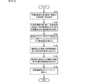
- FIG. 1 is an external perspective view of a semiconductor component according to a first embodiment of the present invention. It is a flowchart which shows the manufacturing method of the semiconductor component which concerns on the 1st Embodiment of this invention.
- (A) is side surface sectional drawing which shows the formation process of the functional member of the semiconductor component which concerns on the 1st Embodiment of this invention
- (B) is the inversion of the semiconductor component which concerns on the 1st Embodiment of this invention It is side surface sectional drawing which shows the process of arrangement
- (C) is side surface sectional drawing which shows the formation process of the insulating resin material of the semiconductor component which concerns on the 1st Embodiment of this invention
- (D) is this It is side surface sectional drawing which shows the thin film formation process of the semiconductor component which concerns on the 1st Embodiment of invention
- (E) is the side surface which shows the division
- FIG. 1 is a side sectional view showing a main configuration of a semiconductor component according to the first embodiment of the present invention.
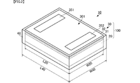
- FIG. 2 is an external perspective view of the semiconductor component according to the first embodiment of the present invention.
- the semiconductor component 10 includes a semiconductor substrate 20, a rewiring layer 30, and an insulating layer 40.
- the semiconductor substrate 20 is, for example, a Si substrate.
- the semiconductor substrate 20 is rectangular in plan view.
- the semiconductor substrate 20 includes a first surface 201, a second surface 202, and a side surface 210.
- the first surface 201 and the second surface 202 face each other.
- the side surface 210 is a surface orthogonal to the first surface 201 and the second surface 202, and connects each side of the first surface 201 and each side of the second surface 202.
- a semiconductor element portion 21 is formed in a region on the first surface 201 side of the semiconductor substrate 20.
- the semiconductor element portion 21 has a predetermined depth and a planar shape.
- the semiconductor element portion 21 is formed using a known semiconductor process. For example, in the embodiment shown in FIG. 1, an n-type semiconductor layer (n-type well) having a predetermined depth is formed on the first surface 201 side of the semiconductor substrate 20. In the n-type semiconductor layer, two p-type semiconductor portions are formed apart from each other. The two p-type semiconductor parts are exposed on the first surface 201. The exposed portions of the two p-type semiconductor portions are input / output terminals of a semiconductor element formed by the semiconductor element portion 21. With this configuration, two pn junction diodes are formed in which the cathodes are connected to each other and the anodes are exposed on the first surface 201, respectively. Thereby, the semiconductor component 10 can be used as an ESD protection element.
- the rewiring layer 30 is rectangular in plan view, and its area is the same as the area of the semiconductor substrate 20.
- the rewiring layer 30 is in contact with and bonded to the first surface 201 of the semiconductor substrate 20.
- the redistribution layer 30 includes insulating layers 31 and 32 and redistribution conductors 341 and 342. More specifically, the insulating layer 31 and the insulating layer 32 are laminated in this order from the first surface 201 side. Insulating layer 31 is made of, for example, of SiO 2. The passivation layer of the semiconductor substrate 20 may be the insulating layer 31. The insulating layer 32 is made of, for example, an insulating resin.
- the rewiring conductors 341 and 342 are made of, for example, Al.
- One end of the redistribution conductor 341 is connected to a portion of the semiconductor substrate 20 where one p-type semiconductor portion is exposed.
- the other end of the redistribution conductor 341 is disposed closer to the side surface of the semiconductor component 10 than the one end of the redistribution conductor 341.
- the other end of the redistribution conductor 341 is exposed to the outside through a hole formed in the insulating layer 32.
- One end of the redistribution conductor 342 is connected to a portion of the semiconductor substrate 20 where the other p-type semiconductor portion is exposed.
- the other end of the redistribution conductor 342 is disposed closer to the side of the semiconductor component 10 than the one end of the redistribution conductor 342.
- the other end of the redistribution conductor 342 is exposed to the outside through a hole formed in the insulating layer 32.
- These portions where the redistribution conductors 341 and 342 are exposed are external connection terminals of the semiconductor component 10.
- the exposed surface may be plated.
- Au plating with Ni as a base can be used. With this configuration, the surface of the rewiring layer 30 opposite to the surface in contact with the semiconductor substrate 20, that is, the outer surface of the insulating layer 32 becomes the back surface 301 of the semiconductor component 10.
- the insulating layer 40 is made of an insulating resin material.
- the insulating layer 40 is made of an epoxy resin or the like.
- the insulating layer 40 contacts the entire side surface 210 of the semiconductor substrate 20 and is bonded to the side surface 210.
- an insulating adhesive may be used between the insulating layer 40 and the side surface 210. That is, the contact between the insulating layer 40 and the side surface 210 is a state in which the insulating layer 40 and the side surface 210 are directly bonded, or the insulating layer 40 and the side surface 210 are bonded using an insulating adhesive or the like. Any of the states may be used.
- the insulating layer 40 contacts the entire surface of the second surface 202 of the semiconductor substrate 20 and is bonded to the second surface 202. That is, the contact between the insulating layer 40 and the second surface 202 is a state where the insulating layer 40 and the second surface 202 are directly joined, or the insulating layer 40 and the second surface 202 are an insulating adhesive or the like. Any of the states of joining using the As described above, the insulating layer 40 is continuously in contact with the second surface 202 from all the side surfaces 210 of the semiconductor substrate 20, and is in contact with and bonded to all the side surfaces 210 and the second surface 202. Yes.
- the insulating layer 40 also abuts on all the side surfaces of the rewiring layer 30 and is joined to all these side surfaces. Further, the insulating layer 40 is not in contact with the surface of the rewiring layer 30 opposite to the surface in contact with the semiconductor substrate 20, that is, the back surface 301 of the semiconductor component 10.
- the insulating layer 40 covers all the side surfaces of the semiconductor substrate 20, all the side surfaces of the redistribution layer 30, and the second surface 202 of the semiconductor substrate 20, and is related to the back surface 301 of the semiconductor component 10. Is arranged so that there is no. In other words, the entire back surface 301 of the semiconductor component 10 is exposed to the outside.
- the insulating layer 40 is continuously in contact with the side surface 210 and the second surface 202 which are orthogonal to each other in the semiconductor substrate 20. Therefore, when the semiconductor component 10 is mounted on the external circuit board, the insulating layer 40 hardly falls off the semiconductor substrate 20 even if an impact is applied.
- the semiconductor substrate 20 and the insulating layer 40 have a difference in thermal expansion coefficient due to the difference in material. Therefore, peeling may occur at the interface between the semiconductor substrate 20 and the insulating layer 40. However, even if peeling occurs, the state in which the semiconductor substrate 20 is covered with the insulating layer 40 does not change. Thereby, even if there is an external undesired conductor, the side surface 210 and the second surface 202 of the semiconductor substrate 20 are not short-circuited to the undesired conductor, and the electrical reliability of the semiconductor component 10 is high.
- a highly reliable semiconductor component 10 can be realized by using the configuration of the present embodiment.
- the insulating layer 40 may not be in contact with the side surface of the rewiring layer 30. However, the reliability of the semiconductor component 10 is further improved because the insulating layer 40 is also in contact with the side surface of the rewiring layer 30.
- FIG. 3 is a flowchart showing a method for manufacturing a semiconductor component according to the first embodiment of the present invention.
- FIG. 4 is a side sectional view showing the configuration of the manufacturing process of the semiconductor component according to the first embodiment of the present invention.
- FIG. 4A shows a functional member forming process
- FIG. 4B shows an inversion arrangement process
- FIG. 4C shows an insulating resin material forming process
- FIG. 4D shows a thinning process
- FIG. 4E shows a dividing process into individual pieces.
- a mother semiconductor substrate 200 made of SiO 2 or the like is prepared, and a plurality of semiconductor element portions 21 are formed on the first surface 201 side of the mother semiconductor substrate 200 (S101).
- the plurality of semiconductor element portions 21 are formed so as to be arranged at intervals with respect to the mother semiconductor substrate 200.
- the rewiring layer 30 is formed on the first surface 201 side of the mother semiconductor substrate 200 (S102).
- a rewiring conductor is formed for each of the plurality of semiconductor element portions 21.
- FIG. 4A a plurality of functional members 100 each having a semiconductor element portion 21 formed on the semiconductor substrate 200 and a rewiring layer conductor formed on the rewiring layer 30 are formed. Is done.
- the second direction dimension W20 of the functional member 100 is smaller than the second direction dimension W40 of the semiconductor component 10 by a predetermined length.
- L40 ⁇ W40 1.0 [mm] ⁇ 0.5 [mm]
- L20 ⁇ W20 0.9 [mm] ⁇ 0.4 [mm].
- This dimensional difference is determined by the film thickness of the insulating layer 40, and the dimensional difference is approximately twice the film thickness of the insulating layer 40.
- the arrangement state is maintained even if the functional members 100 are separated into individual pieces.
- the plurality of functional members 100 are reversed, and the back surface 301 (the outer surface on the rewiring layer 30 side) of the functional member 100 is attached to the surface of the holding plate 902 (S104). Since the plurality of functional members 100 are inverted while being attached to the dicing tape 901, they are attached to the surface of the holding plate 902 while maintaining the arrangement state.
- an insulating resin material (insulating layer 40) that covers the surface of the holding plate 902 and the plurality of functional members 100 is formed (S105).
- the insulating resin material (insulating layer 40) is made of epoxy resin or the like as described above.
- the insulating layer 40 having the desired color can be realized by including a filler or pigment having the desired color.
- the insulating resin material (insulating layer 40) is polished to form the insulating layer 40 having a predetermined thickness. Thereby, the semiconductor component 10 is made thin. If the thickness can be adjusted at the time of forming the insulating resin material, the step of polishing the insulating resin material (insulating layer 40) can be omitted.
- the insulating resin material (insulating layer 40) between the plurality of functional members 100 is diced into a plurality of semiconductor components 10 in plan view (S106). Then, each semiconductor component 10 is peeled from the holding plate 902.
- the side surface 210, the second surface 202 of the semiconductor substrate 20 and the side surface of the rewiring layer 30 are brought into contact with each other, and the outer surface of the rewiring layer 30 (semiconductor component 10 (functional member 100).
- the insulating layer 40 can be easily formed irrespective of the back surface 301).
- the insulating layer 40 can be simultaneously formed on the plurality of functional members 100 by using the above-described manufacturing method. Thereby, the productivity of the semiconductor component 10 is improved.
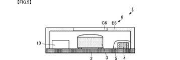
- FIG. 5 is a side sectional view showing the main configuration of the white light emitting diode device according to the embodiment of the present invention.
- the white light emitting diode device 1 includes a semiconductor component 10, a circuit board 2, a white light emitting diode (LED) 3, a mounting electronic component 4, a resin mold 5, and a lid member 6.
- a semiconductor component 10 As shown in FIG. 5, the white light emitting diode device 1 includes a semiconductor component 10, a circuit board 2, a white light emitting diode (LED) 3, a mounting electronic component 4, a resin mold 5, and a lid member 6.
- LED white light emitting diode
- the circuit board 2 is made of, for example, an alumina substrate, and a predetermined circuit conductor pattern is formed.
- the white light emitting diode 3, the mountable electronic component 4, and the semiconductor component 10 are mounted on the surface of the circuit board 2.
- the semiconductor component 10 has the above-described configuration and functions as an ESD protection element.
- the semiconductor component 10 and the white light emitting diode 3 are connected in parallel.
- the insulating layer 40 of the semiconductor component 10 is white.
- the term “white” includes not only white in a strict sense but also milky white, cloudy color, and other colors close to white.
- the mounted electronic component 4 is a capacitor or the like.
- the mounting electronic component 4 is covered with a resin mold 5.
- the lid member 6 has translucency. Specifically, the lid member 6 includes a first light transmitting part C6 and a second light transmitting part E6.
- the white light transmittance of the first light transmitting portion C6 is higher than the white light transmittance of the second light transmitting portion E6.
- the first light transmitting portion C6 is disposed at the center, and the second light transmitting portion E6 surrounds the first light transmitting portion C6.
- the lid member 6 is disposed on the surface (mounting surface) side of the circuit board 2 on which the white light emitting diode 3, the mounted electronic component 4, and the semiconductor component 10 are mounted.
- the end of the lid member 6 is in contact with the mounting surface of the circuit board 2. With this configuration, the white light emitting diode 3, the mountable electronic component 4, and the semiconductor component 10 are arranged in a space sealed by the circuit board 2 and the lid member 6.
- the semiconductor component 10 functioning as an ESD protection element.
- the insulating layer 40 of the semiconductor component 10 is white, the white light emitted from the white light emitting diode 3 and propagated to the semiconductor component 10 is reflected by the insulating layer 40. Thereby, the light emitted from the white light emitting diode 3 is not absorbed by the semiconductor component 10, and the light emission efficiency of the white light emitting diode device 1 is improved.
- the semiconductor component 10 does not have to be covered with a white resin mold, and the white light emitting diode device 1 is realized with a simpler configuration.
- the white light-emitting diode device 1 having high reliability and good luminous efficiency can be realized with a simple configuration.
- transistors and the like can be formed by changing the configurations of the semiconductor element portion 21 and the rewiring layer 30.
Landscapes
- Led Device Packages (AREA)
- Structures Or Materials For Encapsulating Or Coating Semiconductor Devices Or Solid State Devices (AREA)
Abstract
信頼性の高い半導体部品を実現する。半導体部品(10)は、半導体基板(20)、半導体素子部(21)、再配線層(30)、および、絶縁層(40)を備える。半導体基板(20)は、互いに対向する第1面(201)と第2面(202)、および、第1面(201)と第2面(202)に直交する側面(210)を有する。半導体素子部(21)は、半導体基板(20)の第1面(201)側の領域に形成されている。再配線層(30)は、半導体基板(20)の第1面(201)に形成されている。絶縁層(40)は、半導体基板(20)の側面(210)と第2面(202)とに亘って当接している。さらに、絶縁層(40)は、再配線層(30)における半導体基板(20)に当接する面と反対側となる半導体部品(10)の裏面(301)に係らない。
Description
本発明は、半導体素子部が形成された半導体基板と再配線層とを備える半導体部品、当該半導体部品を備える白色発光ダイオードデバイス、および、半導体部品の製造方法に関する。
電子部品の小型化に伴って、実装型の半導体部品も小型化が進んでいる。その1つの手法として、チップ寸法パッケージがあり、多く実用化されている。
チップ寸法パッケージの半導体部品では、再配線層は半導体基板の一面に形成されている。このため、半導体基板の側面は外部に露出しており、信頼性低下の要因になり得る。この問題を解決する構成として、特許文献1、2に記載の半導体部品は、半導体基板および再配線層の側面に絶縁膜を備えている。
しかしながら、特許文献1、2の構成からなる半導体部品では、半導体部品を回路基板に実装する際の衝撃によって、側面の絶縁膜が脱落してしまうことがある。
また、半導体部品が実装された状態において、回路基板に衝撃が加わると、この衝撃によって、側面の絶縁膜が脱落してしまうことがある。
さらには、半導体基板の材料と側面の絶縁膜の材料とは異なり、線膨張係数も異なる。このため、半導体基板と側面の絶縁膜との界面に剥離が生じ易い。特許文献2の構成では、側面の絶縁膜は、半導体部品の裏面も覆っている。この場合、当該剥離によって、半導体部品の裏面に形成されたバンプの脱落という不具合、バンプに接続するメタルポスト(再配線層の裏面から突出する導体)の破損という不具合が発生し易い。
このように、特許文献1、2の構成からなる半導体部品では、信頼性に不安な面がある。
したがって、本発明の目的は、信頼性の高い半導体部品を提供することにある。
この発明の半導体部品は、半導体基板、半導体素子部、再配線層、および、絶縁層を備える。半導体基板は、互いに対向する第1面と第2面、および、第1面と第2面に直交する側面を有する。半導体素子部は、半導体基板の第1面側の領域に形成されている。再配線層は、半導体基板の第1面に形成されている。絶縁層は、半導体基板の側面と第2面とに亘って当接している。さらに、絶縁層は、再配線層における半導体基板に当接する面と反対側の面に係らない形状である。
この構成では、半導体基板は、絶縁層によって外部の不所望な導体と短絡せず、半導体基板からの絶縁層の脱落は、殆ど生じない。
また、この発明の半導体部品では、絶縁層は、半導体基板の側面から再配線層の側面に亘って当接していることが好ましい。
この構成では、半導体基板からの絶縁層の脱落は、さらに確実に抑制される。
また、この発明の半導体部品では、半導体素子部は、pn接合を利用したダイオードであってもよい。
この構成では、半導体部品として、ESD保護部品を実現できる。したがって、信頼性の高いESD保護部品を実現できる。
また、この発明の半導体部品は、絶縁層は白色であることが好ましい。
この構成では、半導体部品に照射された光はそのまま低損失で反射する。したがって、光を反射したい環境に半導体部品を配置する場合に有効である。
また、この発明の白色発光ダイオードデバイスは、上述のESD保護部材として機能する半導体部品、白色発光ダイオード、回路基板、および、蓋部材を備える。白色発光ダイオードは、半導体部品に並列接続されている。回路基板は、半導体部品と白色発光ダイオードとが実装されている。蓋部材は、透光性を有する。蓋部材は、回路基板における半導体部品と白色発光ダイオードとが実装される面側に配置されている。半導体部品と白色発光ダイオードとは、回路基板と蓋部材とによって密閉される空間内に配置されている。半導体部品の絶縁層は白色である。
この構成では、ESD保護部材として機能する半導体部品によって、過電流による白色発光ダイオードの破壊が保護される。また、白色発光ダイオードから出光し、半導体部材に伝搬した光は、半導体部品の絶縁層で反射される。これにより、半導体部品で光が吸収されることによる光の損失が抑制され、白色発光ダイオードデバイスの発光効率が向上する。
また、この発明の半導体部品の製造方法は、次の各工程を有する。この製造方法は、半導体基板の第1面側の領域に複数の半導体素子部を形成する工程を有する。この製造方法は、複数の半導体素子部毎に再配線導体を有する再配線層を半導体基板の第1面に形成することで、それぞれが半導体素子部と再配線導体とを有する複数の機能部材を形成する工程を有する。この製造方法は、半導体基板の第1面に対向する第2面にダイシングテープを貼り付け、機能部材を含む最終形状の半導体部品の形状よりも小さい寸法で、半導体基板と再配線層を切断して、複数の機能部材に個片化する工程を有する。この製造方法は、複数の機能部材における再配線層側の外面を保持板の表面に貼り付ける工程を有する。この製造方法は、保持板の表面および複数の機能部材を覆う絶縁性樹脂材を形成する工程を有する。この製造方法は、絶縁性樹脂材を切断して、機能部材と絶縁性樹脂材とを備える半導体部品に個片化する工程を有する。
この製造方法によって製造される半導体部品では、絶縁層は、半導体基板の側面から第2面に亘って形成され、再配線層における半導体基板と当接する面と反対側の面に係らない形状である。したがって、このような絶縁層の構成を有する信頼性の高い半導体部品を容易に製造できる。
この発明によれば、信頼性の高い半導体部品を実現できる。
本発明の第1の実施形態に係る半導体部品および半導体部品の製造方法について、図を参照して説明する。図1は、本発明の第1の実施形態に係る半導体部品の主要構成を示す側面断面図である。図2は、本発明の第1の実施形態に係る半導体部品の外観斜視図である。
図1、図2に示すように、半導体部品10は、半導体基板20、再配線層30、および、絶縁層40を備える。
半導体基板20は、例えばSi基板である。半導体基板20は、平面視して矩形である。
半導体基板20は、第1面201、第2面202、および、側面210を備える。第1面201と第2面202とは互いに対向している。側面210は、第1面201と第2面202とに対して直交する面であり、第1面201の各辺と第2面202の各辺を接続している。
半導体基板20の第1面201側の領域には、半導体素子部21が形成されている。半導体素子部21は、所定の深さおよび平面形状である。半導体素子部21は、既知の半導体プロセスを用いて形成されている。例えば、図1に示す態様では、半導体基板20の第1面201側に、所定の深さのn型半導体層(n型ウェル)が形成されている。n型半導体層内には、2つのp型半導体部が、離間して形成されている。2つのp型半導体部は、第1面201に露出している。この2つのp型半導体部の露出部は、半導体素子部21によって形成される半導体素子の入出力端子である。この構成により、互いにカソードが接続され、アノードがそれぞれ第1面201に露出する2つのpn接合のダイオードが形成されている。これにより、半導体部品10は、ESD保護素子として利用可能である。
再配線層30は平面視して矩形であり、その面積は、半導体基板20の面積と同じである。再配線層30は、半導体基板20の第1面201に当接して、接合している。
再配線層30は、絶縁層31、32、および、再配線導体341、342を備える。より具体的には、絶縁層31と絶縁層32は、第1面201側からこの順に積層されている。絶縁層31は、例えば、SiO2からなる。半導体基板20のパッシベーション層を、絶縁層31としてもよい。絶縁層32は、例えば、絶縁性樹脂からなる。
再配線導体341、342は、例えば、Alからなる。再配線導体341の一方端は、半導体基板20における一方のp型半導体部が露出する部分に接続している。再配線導体341の他方端は、再配線導体341の一方端よりも、半導体部品10の側面側に配置されている。再配線導体341の他方端は、絶縁層32に形成された孔によって、外部に露出している。再配線導体342の一方端は、半導体基板20における他方のp型半導体部が露出する部分に接続している。再配線導体342の他方端は、再配線導体342の一方端よりも、半導体部品10の側面側に配置されている。再配線導体342の他方端は、絶縁層32に形成された孔によって、外部に露出している。これら、再配線導体341、342が露出する部分は、半導体部品10の外部接続端子である。なお、この露出面には、メッキ処理が施されていてもよい。メッキとしては、Niを下地としたAuメッキ等を用いることができる。この構成により、再配線層30における半導体基板20に当接する面と反対側の面、すなわち、絶縁層32の外面は、半導体部品10の裏面301となる。
絶縁層40は、絶縁性を有する樹脂材料からなる。例えば、絶縁層40は、エポキシ樹脂等からなる。絶縁層40は、半導体基板20の側面210の全面に当接し、該側面210に接合されている。この際、絶縁層40と側面210との間には、絶縁性の接着材を用いることも可能である。すなわち、絶縁層40と側面210との当接は、絶縁層40と側面210とが直接接合される状態、または、絶縁層40と側面210とが絶縁性の接着材等を用いて接合される状態のいずれであってもよい。さらに、絶縁層40は、半導体基板20の第2面202の全面に当接し、該第2面202に接合されている。すなわち、絶縁層40と第2面202との当接は、絶縁層40と第2面202とが直接接合される状態、または、絶縁層40と第2面202とが絶縁性の接着材等を用いて接合される状態のいずれであってもよい。このように、絶縁層40は、半導体基板20の全ての側面210から第2面202に亘って連続して当接しており、全ての側面210と第2面202とに当接し、接合されている。
また、絶縁層40は、再配線層30の全ての側面にも当接し、これら全ての側面に接合されている。さらに、絶縁層40は、再配線層30における半導体基板20に当接する面と反対側の面、すなわち、半導体部品10の裏面301に当接していない。
すなわち、絶縁層40は、半導体基板20の全側面、再配線層30の全側面、および、半導体基板20の第2面202に対して、これらの全面を覆い、半導体部品10の裏面301に係らないように配置されている。言い換えれば、半導体部品10の裏面301の全面は、外部に露出している。
このような構成とすることによって、外部に不所望な導体があっても、半導体基板20の側面210および第2面202は、この不所望な導体に短絡しない。これにより、半導体部品10の電気的な信頼性は高い。
また、半導体基板20における互いに直交する側面210と第2面202とに絶縁層40が連続的に当接している。したがって、半導体部品10を外部の回路基板に実装する際に、衝撃が加わっても、絶縁層40は、半導体基板20から殆ど脱落しない。
また、半導体基板20と絶縁層40とは、その材料の差から、熱膨張係数の差を有する。したがって、半導体基板20と絶縁層40との界面で剥離が生じる可能性がある。しかしながら、剥離が生じたとしても、半導体基板20が絶縁層40によって覆われている状態は変化しない。これにより、外部の不所望な導体があっても、半導体基板20の側面210および第2面202は、この不所望な導体に短絡せず、半導体部品10の電気的な信頼性は高い。
以上のように、本実施形態の構成を用いることによって、信頼性の高い半導体部品10を実現できる。
なお、絶縁層40は、再配線層30の側面に当接していなくてもよい。しかしながら、再配線層30の側面にも絶縁層40が当接していることによって、半導体部品10の信頼性はさらに向上する。
このような構成からなる半導体部品10は、次に示す製造方法によって製造される。図3は、本発明の第1の実施形態に係る半導体部品の製造方法を示すフローチャートである。図4は、本発明の第1の実施形態に係る半導体部品の製造過程の構成を示す側面断面図である。
図4(A)は、機能部材の形成工程を示し、図4(B)は、反転配置の工程を示す。図4(C)は、絶縁性樹脂材の形成工程を示し、図4(D)は、薄膜化工程を示し、図4(E)は、個片への分断工程を示す。
以下は、図3のフローチャートにしたがって、図4の各図を参照しながら、半導体部品10の製造方法を説明する。
まず、SiO2等からなるマザーの半導体基板200を用意し、当該マザーの半導体基板200の第1面201側に複数の半導体素子部21を形成する(S101)。複数の半導体素子部21は、マザーの半導体基板200に対して、それぞれに間隔を空けて、配列して形成されている。
次に、マザーの半導体基板200の第1面201側に再配線層30を形成する(S102)。再配線層30には、複数の半導体素子部21毎に、再配線導体が形成されている。これにより、図4(A)に示すように、半導体基板200に形成された半導体素子部21と、再配線層30に形成された再配線層導体とをそれぞれに有する複数の機能部材100が形成される。
複数の機能部材100が形成された状態で、図4(A)に示すように、マザーの半導体基板200および再配線層30は、ダイシングテープ901の表面に貼り付けられる。この際、ダイシングテープ901には、半導体基板200の第2面202が当接している。そして、図4(A)に示すように、マザーの半導体基板200および再配線層30を切断することによって、複数の機能部材100を個片化する(S103)。複数の機能部材100の寸法は、最終形状である半導体部品10の寸法よりも、所定長さだけ小さい。例えば、図2に示すように、機能部材100の第1方向寸法L20は、半導体部品10の第1方向の寸法L40に対して所定長さだけ小さい。また、図2に示すように、機能部材100の第2方向寸法W20は、半導体部品10の第2方向の寸法W40に対して所定長さだけ小さい。例えば、L40×W40=1.0[mm]×0.5[mm]の場合、L20×W20=0.9[mm]×0.4[mm]である。この寸法差は、絶縁層40の膜厚によって決まり、寸法差は絶縁層40の膜厚の略2倍である。
複数の機能部材100は、ダイシングテープ901に貼り付けられているので、個片化されても、その配列状態は維持されている。
次に、図4(B)に示すように、複数の機能部材100を反転させ、機能部材100の裏面301(再配線層30側の外面)を保持板902の表面に貼り付ける(S104)。複数の機能部材100は、ダイシングテープ901に貼り付けられた状態で反転されるので、その配列状態が維持されたまま、保持板902の表面に貼り付けられる。
次に、図4(C)に示すように、保持板902の表面および複数の機能部材100を覆う絶縁性樹脂材(絶縁層40)を形成する(S105)。絶縁性樹脂材(絶縁層40)は、上述のようにエポキシ樹脂等からなる。この際、所望色のフィラーまたは顔料を含ませることによって、所望色の絶縁層40を実現できる。
次に、図4(D)に示すように、絶縁性樹脂材(絶縁層40)を研磨し、所定厚みの絶縁層40を形成する。これにより、半導体部品10を薄型にする。なお、絶縁性樹脂材の形成時に、厚みを調整できる場合には、この絶縁性樹脂材(絶縁層40)の研磨工程は省略できる。
次に、図4(E)に示すように、平面視して、複数の機能部材100間の絶縁性樹脂材(絶縁層40)をダイシングし、複数の半導体部品10に個片化する(S106)。そして、各半導体部品10を保持板902から剥離する。
このような製造方法を用いることによって、半導体基板20の側面210、第2面202、および、再配線層30の側面に亘って当接し、再配線層30の外面(半導体部品10(機能部材100)の裏面301)に係らない絶縁層40を容易に形成できる。この際、上述の製造方法を用いることによって、複数の機能部材100に対して、絶縁層40を同時に形成できる。これにより、半導体部品10の生産性が向上する。
このような構成からなる半導体部品10は、次に示すデバイスに利用される。図5は、本発明の実施形態に係る白色発光ダイオードデバイスの主要構成を示す側面断面図である。
図5に示すように、白色発光ダイオードデバイス1は、半導体部品10、回路基板2、白色発光ダイオード(LED)3、実装型電子部品4、樹脂モールド5、および、蓋部材6を備える。
回路基板2は、例えば、アルミナ基板からなり、所定の回路導体パターンが形成されている。白色発光ダイオード3、実装型電子部品4、および、半導体部品10は、回路基板2の表面に実装されている。半導体部品10は、上述の構成を備え、ESD保護素子として機能する。半導体部品10と白色発光ダイオード3とは、並列接続されている。また、半導体部品10の絶縁層40は白色である。なお、「白色」とは、厳密な意味での白色のみならず、乳白色、白濁色、その他白色に近い色を含む。実装型電子部品4は、キャパシタ等である。実装型電子部品4は、樹脂モールド5によって覆われている。
蓋部材6は、透光性を有する。具体的には、蓋部材6は、第1透光部C6と第2透光部E6とを備える。第1透光部C6の白色光の透過率は、第2透光部E6の白色光の透過率よりも高い。蓋部材6を平面視して、第1透光部C6は、中央に配置され、第2透光部E6は、第1透光部C6を囲んでいる。
蓋部材6は、回路基板2における白色発光ダイオード3、実装型電子部品4、および、半導体部品10が実装される面(実装面)側に配置されている。蓋部材6の端は、回路基板2の実装面に当接している。この構成により、白色発光ダイオード3、実装型電子部品4、および、半導体部品10は、回路基板2と蓋部材6とによって密閉された空間内に配置される。
このような構成とすることによって、ESD保護素子として機能する半導体部品10によって、過電流による白色発光ダイオード3の破損は抑制される。また、半導体部品10の絶縁層40が白色であることによって、白色発光ダイオード3が出射して、半導体部品10に伝搬した白色光は、絶縁層40で反射する。これにより、白色発光ダイオード3から出射された光は、半導体部品10に吸収されず、白色発光ダイオードデバイス1の発光効率は向上する。また、実装型電子部品4のように、白色の樹脂モールドで半導体部品10を覆わなくてよく、白色発光ダイオードデバイス1は、より簡素な構成で実現される。
このように、本実施形態の構成を用いることによって、信頼性が高く、且つ発光効率が良い白色発光ダイオードデバイス1を、簡素な構成で実現できる。
なお、上述の半導体部品10の態様では、半導体部品10でESD保護素子を形成する態様を示した。しかしながら、半導体素子部21および再配線層30の構成を変えることによって、トランジスタ等を形成することもできる。
1:白色発光ダイオードデバイス
2:回路基板
3:白色発光ダイオード
4:実装型電子部品
5:樹脂モールド
6:蓋部材
10:半導体部品
20:半導体基板
21:半導体素子部
30:再配線層
31:絶縁層
32:絶縁層
40:絶縁層
100:機能部材
200:半導体基板
201:第1面
202:第2面
210:側面
301:裏面
341:再配線導体
342:再配線導体
901:ダイシングテープ
902:保持板
C6:蓋部材6の第1透光部
E6:蓋部材6の第2透光部
2:回路基板
3:白色発光ダイオード
4:実装型電子部品
5:樹脂モールド
6:蓋部材
10:半導体部品
20:半導体基板
21:半導体素子部
30:再配線層
31:絶縁層
32:絶縁層
40:絶縁層
100:機能部材
200:半導体基板
201:第1面
202:第2面
210:側面
301:裏面
341:再配線導体
342:再配線導体
901:ダイシングテープ
902:保持板
C6:蓋部材6の第1透光部
E6:蓋部材6の第2透光部
Claims (6)
- 互いに対向する第1面と第2面、および、前記第1面と前記第2面に直交する側面を有する半導体基板と、
前記半導体基板の前記第1面側の領域に形成された半導体素子部と、
前記半導体基板の前記第1面に形成された再配線層と、
前記半導体基板の前記側面と前記第2面とに亘って当接する絶縁層と、を備え、
前記絶縁層は、前記再配線層における前記半導体基板に当接する面と反対側の面に係らない形状である、
半導体部品。 - 前記絶縁層は、前記半導体基板の側面から前記再配線層の側面に亘って当接している、
請求項1に記載の半導体部品。 - 前記半導体素子部は、pn接合を利用したダイオードである、
請求項1または請求項2に記載の半導体部品。 - 前記絶縁層は白色である、
請求項1乃至請求項3のいずれかに記載の半導体部品。 - 請求項3に記載の半導体部品と、
前記半導体部品に並列接続される白色発光ダイオードと、
前記半導体部品と前記白色発光ダイオードとが実装される回路基板と、
透光性を有する蓋部材と、を備え、
前記蓋部材は、前記回路基板における前記半導体部品と前記白色発光ダイオードとが実装される面側に配置され、
前記半導体部品と前記白色発光ダイオードとは、前記回路基板と前記蓋部材とによって密閉される空間内に配置されており、
前記半導体部品の前記絶縁層は白色である、
白色発光ダイオードデバイス。 - 半導体基板の第1面側の領域に複数の半導体素子部を形成する工程と、
前記複数の半導体素子部毎に再配線導体を有する再配線層を前記半導体基板の前記第1面に形成し、それぞれが前記半導体素子部と前記再配線導体とを有する複数の機能部材を形成する工程と、
前記半導体基板の前記第1面に対向する第2面にダイシングテープを貼り付け、前記機能部材を含む最終形状の半導体部品の形状よりも小さい寸法で、前記半導体基板と前記再配線層を切断して、前記複数の機能部材に個片化する工程と、
前記複数の機能部材における前記再配線層側の外面を保持板の表面に貼り付ける工程と、
前記保持板の表面および前記複数の機能部材を覆う絶縁性樹脂材を形成する工程と、
前記絶縁性樹脂材を切断して、前記機能部材と前記絶縁性樹脂材とを備える半導体部品に個片化する工程と、
を有する、半導体部品の製造方法。
Priority Applications (1)
| Application Number | Priority Date | Filing Date | Title |
|---|---|---|---|
| CN201790000362.8U CN208189571U (zh) | 2016-06-16 | 2017-06-08 | 半导体部件以及白色发光二极管器件 |
Applications Claiming Priority (2)
| Application Number | Priority Date | Filing Date | Title |
|---|---|---|---|
| JP2016119890 | 2016-06-16 | ||
| JP2016-119890 | 2016-06-16 |
Publications (1)
| Publication Number | Publication Date |
|---|---|
| WO2017217307A1 true WO2017217307A1 (ja) | 2017-12-21 |
Family
ID=60663542
Family Applications (1)
| Application Number | Title | Priority Date | Filing Date |
|---|---|---|---|
| PCT/JP2017/021253 Ceased WO2017217307A1 (ja) | 2016-06-16 | 2017-06-08 | 半導体部品、白色発光ダイオードデバイス、および半導体部品の製造方法 |
Country Status (2)
| Country | Link |
|---|---|
| CN (1) | CN208189571U (ja) |
| WO (1) | WO2017217307A1 (ja) |
Citations (3)
| Publication number | Priority date | Publication date | Assignee | Title |
|---|---|---|---|---|
| JP2015056379A (ja) * | 2013-09-13 | 2015-03-23 | パナソニックIpマネジメント株式会社 | 照明用光源及び照明装置 |
| JP2015213157A (ja) * | 2014-04-14 | 2015-11-26 | 日亜化学工業株式会社 | 半導体装置 |
| WO2016031684A1 (ja) * | 2014-08-29 | 2016-03-03 | 住友ベークライト株式会社 | 半導体装置の製造方法および半導体装置 |
-
2017
- 2017-06-08 WO PCT/JP2017/021253 patent/WO2017217307A1/ja not_active Ceased
- 2017-06-08 CN CN201790000362.8U patent/CN208189571U/zh active Active
Patent Citations (3)
| Publication number | Priority date | Publication date | Assignee | Title |
|---|---|---|---|---|
| JP2015056379A (ja) * | 2013-09-13 | 2015-03-23 | パナソニックIpマネジメント株式会社 | 照明用光源及び照明装置 |
| JP2015213157A (ja) * | 2014-04-14 | 2015-11-26 | 日亜化学工業株式会社 | 半導体装置 |
| WO2016031684A1 (ja) * | 2014-08-29 | 2016-03-03 | 住友ベークライト株式会社 | 半導体装置の製造方法および半導体装置 |
Also Published As
| Publication number | Publication date |
|---|---|
| CN208189571U (zh) | 2018-12-04 |
Similar Documents
| Publication | Publication Date | Title |
|---|---|---|
| TWI422044B (zh) | 封裝發光裝置之晶片尺度方法及經晶片尺度封裝之發光裝置 | |
| CN105103314B (zh) | 半导体器件和用于制造半导体器件的方法 | |
| JP6892261B2 (ja) | Ledパッケージ | |
| CN103370779B (zh) | 支承衬底和用于制造半导体芯片的方法 | |
| CN105409017B (zh) | 可表面安装的光电子半导体组件和用于制造至少一个可表面安装的光电子半导体组件的方法 | |
| US9153746B2 (en) | Semiconductor light emitting device and method for manufacturing same | |
| US20100237379A1 (en) | Light emitting device | |
| JP6106755B2 (ja) | 組込み保護ダイオードを備えるオプトエレクトロニクスコンポーネントおよびその製造方法 | |
| TWI569475B (zh) | 發光裝置、電路基板、發光裝置用封裝陣列、及發光裝置用封裝陣列之製造方法 | |
| JP2018518039A (ja) | オプトエレクトロニクス部品アレイおよび複数のオプトエレクトロニクス部品アレイを製造する方法 | |
| US10699991B2 (en) | Packaged light emitting devices including electrode isolation structures and methods of forming packaged light emitting devices including the same | |
| JP6210720B2 (ja) | Ledパッケージ | |
| JP5548826B2 (ja) | オプトエレクトロニクス半導体部品の製造方法、およびオプトエレクトロニクス半導体部品 | |
| KR20150037216A (ko) | 발광 디바이스 | |
| WO2017217307A1 (ja) | 半導体部品、白色発光ダイオードデバイス、および半導体部品の製造方法 | |
| JP5148337B2 (ja) | 発光ダイオードチップおよびその製造方法 | |
| JP2007335734A (ja) | 半導体装置 | |
| JP6543391B2 (ja) | 半導体装置 | |
| KR20170085055A (ko) | 광전 반도체 소자 및 광전 반도체 소자를 포함하는 장치 | |
| US20140211436A1 (en) | Circuit board, optoelectronic component and arrangement of optoelectronic components | |
| KR20160113557A (ko) | 반도체 발광소자 및 이를 제조하는 방법 | |
| TW201917915A (zh) | 發光二極體及其製造方法 | |
| JP6311849B1 (ja) | 半導体部品および半導体部品の製造方法 | |
| JP2017050420A (ja) | 半導体発光装置及びその製造方法 | |
| KR20060069375A (ko) | 반도체 엘이디 소자 및 그 제조 방법 |
Legal Events
| Date | Code | Title | Description |
|---|---|---|---|
| 121 | Ep: the epo has been informed by wipo that ep was designated in this application |
Ref document number: 17813205 Country of ref document: EP Kind code of ref document: A1 |
|
| NENP | Non-entry into the national phase |
Ref country code: DE |
|
| 122 | Ep: pct application non-entry in european phase |
Ref document number: 17813205 Country of ref document: EP Kind code of ref document: A1 |
|
| NENP | Non-entry into the national phase |
Ref country code: JP |