WO2017216682A1 - スパッタリング装置およびトランジスタ - Google Patents
スパッタリング装置およびトランジスタ Download PDFInfo
- Publication number
- WO2017216682A1 WO2017216682A1 PCT/IB2017/053341 IB2017053341W WO2017216682A1 WO 2017216682 A1 WO2017216682 A1 WO 2017216682A1 IB 2017053341 W IB2017053341 W IB 2017053341W WO 2017216682 A1 WO2017216682 A1 WO 2017216682A1
- Authority
- WO
- WIPO (PCT)
- Prior art keywords
- oxide
- insulator
- sputtering target
- transistor
- conductor
- Prior art date
- Legal status (The legal status is an assumption and is not a legal conclusion. Google has not performed a legal analysis and makes no representation as to the accuracy of the status listed.)
- Ceased
Links
Images







Classifications
-
- C—CHEMISTRY; METALLURGY
- C23—COATING METALLIC MATERIAL; COATING MATERIAL WITH METALLIC MATERIAL; CHEMICAL SURFACE TREATMENT; DIFFUSION TREATMENT OF METALLIC MATERIAL; COATING BY VACUUM EVAPORATION, BY SPUTTERING, BY ION IMPLANTATION OR BY CHEMICAL VAPOUR DEPOSITION, IN GENERAL; INHIBITING CORROSION OF METALLIC MATERIAL OR INCRUSTATION IN GENERAL
- C23C—COATING METALLIC MATERIAL; COATING MATERIAL WITH METALLIC MATERIAL; SURFACE TREATMENT OF METALLIC MATERIAL BY DIFFUSION INTO THE SURFACE, BY CHEMICAL CONVERSION OR SUBSTITUTION; COATING BY VACUUM EVAPORATION, BY SPUTTERING, BY ION IMPLANTATION OR BY CHEMICAL VAPOUR DEPOSITION, IN GENERAL
- C23C14/00—Coating by vacuum evaporation, by sputtering or by ion implantation of the coating forming material
- C23C14/22—Coating by vacuum evaporation, by sputtering or by ion implantation of the coating forming material characterised by the process of coating
- C23C14/34—Sputtering
-
- H—ELECTRICITY
- H10—SEMICONDUCTOR DEVICES; ELECTRIC SOLID-STATE DEVICES NOT OTHERWISE PROVIDED FOR
- H10D—INORGANIC ELECTRIC SEMICONDUCTOR DEVICES
- H10D30/00—Field-effect transistors [FET]
- H10D30/60—Insulated-gate field-effect transistors [IGFET]
- H10D30/67—Thin-film transistors [TFT]
-
- H—ELECTRICITY
- H10—SEMICONDUCTOR DEVICES; ELECTRIC SOLID-STATE DEVICES NOT OTHERWISE PROVIDED FOR
- H10P—GENERIC PROCESSES OR APPARATUS FOR THE MANUFACTURE OR TREATMENT OF DEVICES COVERED BY CLASS H10
- H10P14/00—Formation of materials, e.g. in the shape of layers or pillars
- H10P14/40—Formation of materials, e.g. in the shape of layers or pillars of conductive or resistive materials
- H10P14/42—Formation of materials, e.g. in the shape of layers or pillars of conductive or resistive materials using a gas or vapour
Definitions
- the present invention relates to an object, a method, or a manufacturing method. Or this invention relates to a process, a machine, a manufacture, or a composition (composition of matter).
- one embodiment of the present invention relates to a metal oxide, a metal oxide manufacturing apparatus, or a method for manufacturing the metal oxide.
- One embodiment of the present invention relates to a semiconductor device, a display device, a liquid crystal display device, a light-emitting device, a power storage device, a memory device, a driving method thereof, or a manufacturing method thereof.
- a semiconductor device refers to all devices that can function by utilizing semiconductor characteristics.
- a semiconductor element such as a transistor, a semiconductor circuit, an arithmetic device, and a memory device are one embodiment of the semiconductor device.
- An imaging device, a display device, a liquid crystal display device, a light emitting device, an electro-optical device, a power generation device (including a thin film solar cell, an organic thin film solar cell, and the like) and an electronic device may include a semiconductor device.
- Oxide semiconductors are attracting attention as semiconductor materials applicable to transistors.
- a plurality of oxide semiconductor layers are stacked, and among the plurality of oxide semiconductor layers, the oxide semiconductor layer serving as a channel contains indium and gallium, and the proportion of indium is the proportion of gallium.
- a semiconductor device in which the field effect mobility (which may be simply referred to as mobility or ⁇ FE) is increased by increasing the field effect mobility has been studied.
- Non-Patent Document 1 a structure in which an oxide semiconductor having a two-layer structure of an In—Zn oxide and an In—Ga—Zn oxide is studied as an active layer of a transistor.
- Non-Patent Document 2 discusses a configuration in which a metal oxide is used as an active layer of a transistor and the metal oxide has an X—O—Y structure.
- an S value also referred to as Subthreshold Swing, SS
- a threshold voltage also referred to as Vth
- Vth which is one of transistor characteristics is ⁇ 2.9 V, which is a so-called normally-on transistor characteristic.
- a transistor using an oxide semiconductor film for a channel region preferably has higher field-effect mobility.
- the field-effect mobility of a transistor is increased, there is a problem that the characteristics of the transistor tend to be normally on. Note that normally-on refers to a state in which a channel exists even when no voltage is applied to the gate electrode, and current flows through the transistor.
- Non-Patent Document 2 exemplifies a configuration in which a metal oxide has an X—O—Y structure, and is shared with X—O having an ionic bond (X is In, Ga, Zn, Cd, or the like).
- Y—O having a bond (Y is B, Si, Ge, Al, etc.) is integrated. Note that oxygen vacancies in the metal oxide are suppressed by integrating X, which has a low bondability with oxygen (O), and Y, which has a high bondability with oxygen (O).
- Non-Patent Document 2 does not disclose functionally separating X—O and Y—O contained in a metal oxide.
- an object of one embodiment of the present invention is to provide a novel metal oxide. Another object of one embodiment of the present invention is to provide a novel sputtering apparatus. Another object of one embodiment of the present invention is to impart favorable electrical characteristics to a semiconductor device. Another object is to provide a highly reliable semiconductor device. Another object is to provide a semiconductor device with a novel structure.
- One embodiment of the present invention includes a first sputtering target, a second sputtering target, a shutter, and a substrate holder, and the first sputtering target includes a conductive material, and the second sputtering target Includes an insulating material, the shutter is located between the first sputtering target and the second sputtering target and the substrate holder, the shutter is provided with a notch, and the substrate holder is provided with the notch of the shutter. It is a sputtering apparatus characterized by facing a 1st sputtering target or a 2nd sputtering target through a part.
- Another embodiment of the present invention includes a first sputtering target, a second sputtering target, a shutter, and a substrate holder, and the first sputtering target includes a conductive material,
- the sputtering target 2 includes an insulating material, the shutter is positioned between the first sputtering target and the second sputtering target, and the substrate holder, the shutter is provided with an opening, and the substrate holder is the shutter.
- It is a sputtering apparatus characterized by facing a 1st sputtering target or a 2nd sputtering target through this opening part.
- the conductive material preferably has one or both of an oxide of indium and an oxide of zinc.
- the insulating material is element M (element M is Ga, Al, Si, B, Y, Ti, Fe, Ni, Ge, Zr, Mo, La, Ce, Nd, Hf, Ta, It is preferable to have an oxide of any one of W, Mg, V, Be, or Cu or a plurality thereof.
- the shutter can be rotated about an axis perpendicular to the shutter as a rotation axis.
- the first sputtering target and the second sputtering target can be rotated about an axis perpendicular to the shutter as a rotation axis.
- the present invention includes a first sputtering target, a second sputtering target, a third sputtering target, a shutter, and a substrate holder.
- the first sputtering target is: Indium oxide is included, the second sputtering target includes zinc oxide, and the third sputtering target is an element M (element M is Ga, Al, Si, B, Y, Ti, Fe, Ni, Ge , Zr, Mo, La, Ce, Nd, Hf, Ta, W, Mg, V, Be, or Cu), and the shutter includes the first sputtering target, the first sputtering target, 2 and the third sputtering target and the substrate holder, the shutter is provided with a notch, and the substrate Holder via the notch portion of the shutter, the first sputtering target, or is opposed to the second sputtering target or the third sputtering target, it is sputtering apparatus according to claim.
- Another embodiment of the present invention includes a first sputtering target, a second sputtering target, a third target, a shutter, and a substrate holder.
- the first sputtering target is indium.
- the second sputtering target contains an oxide
- the third sputtering target contains an element M (the element M is Ga, Al, Si, B, Y, Ti, Fe, Ni, Ge, Zr, Mo, La, Ce, Nd, Hf, Ta, W, Mg, V, Be, or Cu)
- the shutter includes the first sputtering target, the second,
- the sputtering target is located between the sputtering target and the third sputtering target and the substrate holder, the shutter is provided with an opening, and the substrate holder is shut. Through the opening, the first sputtering target, or is opposed to the second sputtering target or the third sputtering target, it is sputtering apparatus according to claim.
- the shutter can be rotated about an axis perpendicular to the shutter as a rotation axis.
- the first sputtering target, the second sputtering target, and the third sputtering target can be rotated about an axis perpendicular to the shutter.
- the substrate holder can be rotated about an axis perpendicular to the shutter as a rotation axis.
- One embodiment of the present invention includes a gate electrode, a first conductor, a second conductor, a gate insulator, a first oxide, a second oxide, and a third oxide.
- the gate insulator is located between the gate electrode and the first oxide, and the gate electrode overlaps with the second oxide through the gate insulator and the first oxide.
- the first conductor and the second conductor have a region in contact with the top surface and the side surface of the second oxide, and the second oxide has a region in contact with the top surface of the third oxide.
- the second oxide is alternately an oxide having a first band gap in the film thickness direction and an oxide having a second band gap in contact with the oxide having the first band gap.
- the second oxide has two or more layers of oxides having the first band gap. Bandgap second smaller band gap, a transistor, characterized in that.
- the second oxide has a channel formation region
- the first oxide is disposed so as to cover the second oxide in the channel width direction of the channel formation region. It is a transistor.
- the second oxide is a transistor including an oxide having a first band gap and having three to ten layers.
- the transistor is characterized in that the band gap of the first oxide and the band gap of the third oxide are larger than the first band gap.
- the oxide film having the first band gap has a thickness of 0.5 nm to 2.0 nm in the transistor.
- the oxide film having the second band gap has a region of 0.1 nm to 3.0 nm in thickness of the transistor.
- the distance between the end portion of the first conductor and the end portion of the second conductor facing each other has a region of 10 nm to 300 nm.
- the transistor is characterized in that the gate electrode has a width of 10 nm to 300 nm.
- the carrier density of the oxide having the first band gap is 6 ⁇ 10 18 cm ⁇ 3 or more and 5 ⁇ 10 20 cm ⁇ 3 or less.
- the transistor may be characterized in that the oxide having the first band gap is degenerated.
- the oxide having the first band gap includes any one or more of indium, zinc, and nitrogen.
- the oxide having the second band gap includes any one or more of indium, boron, gallium, and zinc.
- a novel metal oxide can be provided.
- a novel sputtering apparatus can be provided.
- favorable electrical characteristics can be imparted to a semiconductor device.
- a highly reliable semiconductor device can be provided.
- a semiconductor device with a novel structure can be provided.
- 10A and 10B illustrate a top view and a cross-sectional view structure of a transistor.
- 3A and 3B illustrate a cross-sectional structure of a transistor.
- 4A and 4B illustrate a top view and a cross-sectional structure of a transistor.
- 10A and 10B are a top view and cross-sectional views illustrating a method for manufacturing a transistor.
- FIG. 6 is a cross-sectional view of a semiconductor device according to one embodiment of the present invention.
- FIG. 6 is a cross-sectional view of a semiconductor device according to one embodiment of the present invention.
- FIG. 6 is a cross-sectional view of a semiconductor device according to one embodiment of the present invention.
- FIG. 6 shows a band of a metal oxide according to one embodiment of the present invention.
- a transistor is an element having at least three terminals including a gate, a drain, and a source.
- a channel region is provided between the drain (drain terminal, drain region or drain electrode) and the source (source terminal, source region or source electrode), and between the source and drain through the channel formation region.
- a current can flow. Note that in this specification and the like, a channel region refers to a region through which a current mainly flows.
- the functions of the source and drain may be switched when transistors with different polarities are used or when the direction of current changes during circuit operation. Therefore, in this specification and the like, the terms source and drain can be used interchangeably.
- “electrically connected” includes a case of being connected via “something having an electric action”.
- the “thing having some electric action” is not particularly limited as long as it can exchange electric signals between connection targets.
- “thing having some electric action” includes electrodes, wiring, switching elements such as transistors, resistance elements, inductors, capacitors, and other elements having various functions.
- a silicon oxynitride film refers to a film having a higher oxygen content than nitrogen as the composition, and a silicon nitride oxide film has a nitrogen content as compared to oxygen as a composition. Refers to membranes with a lot of
- parallel means a state in which two straight lines are arranged at an angle of ⁇ 10 ° to 10 °. Therefore, the case of ⁇ 5 ° to 5 ° is also included.
- substantially parallel means a state in which two straight lines are arranged at an angle of ⁇ 30 ° to 30 °.
- Vertical refers to a state in which two straight lines are arranged at an angle of 80 ° to 100 °. Therefore, the case of 85 ° to 95 ° is also included.
- substantially vertical means a state in which two straight lines are arranged at an angle of 60 ° to 120 °.
- the terms “film” and “layer” can be interchanged with each other depending on circumstances.
- the term “conductive layer” may be changed to the term “conductive film”.
- the term “insulating film” may be changed to the term “insulating layer” in some cases.
- the semiconductor device may have characteristics as an “insulator”.
- the boundary between “semiconductor” and “insulator” is ambiguous and may not be strictly discriminated. Therefore, a “semiconductor” in this specification can be called an “insulator” in some cases.
- an “insulator” in this specification can be called a “semiconductor” in some cases.
- a metal oxide is a metal oxide in a broad expression.
- Metal oxides are classified into oxide insulators, oxide conductors (including transparent oxide conductors), oxide semiconductors (also referred to as oxide semiconductors or simply OS), and the like.
- oxide semiconductors also referred to as oxide semiconductors or simply OS
- the metal oxide may be referred to as an oxide semiconductor. That is, in the case of describing as an OS FET, it can be said to be a transistor including a metal oxide or an oxide semiconductor.
- the metal oxide described in this embodiment preferably contains at least indium. In particular, it is preferable to contain indium and zinc.
- element M element M is Ga, Al, Si, B, Y, Ti, Fe, Ni, Ge, Zr, Mo, La, Ce, Nd, Hf, Ta, W, Mg, Any one or more of V, Be, and Cu).
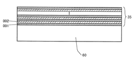
- the metal oxide 35 has a multilayer structure in which layers 001 and 002 are alternately stacked, and can be said to be a structure like a superlattice structure.
- the layer 001 functions as a conductive region
- the layer 002 functions as an insulating region.
- the layer 001 contains indium as a main component
- the layer 002 contains the element M as a main component.
- the metal oxide according to one embodiment of the present invention is a kind of matrix composite material or metal matrix composite material in which materials having different physical properties are mixed.
- the metal oxide which is one embodiment of the present invention includes a region having a conductor function and a region having a dielectric function, and the material as a whole functions as a semiconductor.
- it can also be referred to as CAC (Cloud-Aligned Composite) -OS (Oxide Semiconductor) or CAC-metal oxide.
- the superlattice structure represents a structure in which thin films are laminated periodically or partially and a plurality of laminated films interact with each other.
- the crystal structure of the superlattice structure is not particularly limited.
- the crystal lattice when observed with a high-resolution TEM, the crystal lattice is clearly confirmed in the superlattice structure, and the crystal lattice is not clearly confirmed. Either one or both are included.
- FIG. 1 is a schematic diagram illustrating a sputtering target, a shutter, and a substrate in a film forming chamber of a sputtering apparatus.
- the sputtering apparatus described in this embodiment is provided with a sputtering target 11 a, a sputtering target 11 b, a sputtering target 12, and a notch portion 67 (or a slit portion). And a shutter 66.
- the substrate 60 can be disposed to face the sputtering target 11a, the sputtering target 11b, and the sputtering target 12.
- the sputtering target 11a is disposed on the backing plate 50a.
- the sputtering target 11b is disposed on the backing plate 50b
- the sputtering target 12 is disposed on the backing plate 50c.
- the sputtering target 11a and the sputtering target 11b include a conductive material
- the sputtering target 12 includes an insulating material (also referred to as a dielectric material).
- the layer 001 is a layer mainly composed of sputtered particles of a sputtering target containing a conductive material.
- the layer 002 is a layer mainly composed of sputtered particles of a sputtering target containing an insulating material.
- the conductive material preferably contains indium and / or zinc.
- the conductive material preferably contains indium and / or zinc oxide, nitride and / or oxynitride.
- the above element M (element M is Ga, Al, Si, B, Y, Ti, Fe, Ni, Ge, Zr, Mo, La, Ce, Nd, Hf, Ta, W, Mg) , V, Be, or Cu), or a plurality thereof.
- the insulating material preferably contains an oxide, nitride and / or oxynitride of the element M.
- the sputtering target 11a may include indium oxide
- the sputtering target 11b may include zinc oxide
- the sputtering target 12 may include an oxide of element M.
- the number of sputtering targets is not limited to this. Two or more sputtering targets may be provided in total, that is, at least one sputtering target including a conductive material and one sputtering target including an insulating material.
- the sputtering target may partially have a crystal structure.
- it may have a microcrystalline structure (sometimes referred to as an nc (nano-crystal) structure) or a polycrystalline structure.
- nc nano-crystal
- the diameter of the microcrystal is 0.5 nm to 3 nm, 1 nm to 2 nm, or a value close thereto.
- the shape of the sputtering target 11a, the sputtering target 11b, and the sputtering target 12 is made into disk shape (it can also be called cylindrical shape), the shape of a sputtering target is not limited to this. .
- the shapes of the sputtering target 11a, the sputtering target 11b, and the sputtering target 12 may be a rectangular parallelepiped.
- the shutter 66 is positioned between the sputtering target 11a, the sputtering target 11b, and the sputtering target 12 and the substrate 60 (which can be referred to as a substrate holder on which the substrate 60 is disposed).
- the shutter 66 preferably has a flat shape. It is preferable that one surface of the shutter 66 is opposed to one surface of the sputtering target 11a, the sputtering target 11b, and the sputtering target 12. The other surface of the shutter 66 is preferably opposed to the one surface of the substrate 60.
- the shutter 66 is preferably configured to be rotatable about an axis perpendicular to the upper or lower surface of the shutter 66 (hereinafter sometimes referred to as an axis perpendicular to the shutter 66) as a rotation axis.
- a support for supporting the shutter 66 may be provided from above or below the shutter 66, and a mechanism for rotating the shutter 66 may be provided on the support.
- FIG. 2 shows the shutter 66 as viewed from the substrate 60 side.
- 2A shows a state where the notch 67 of the shutter 66 overlaps with the sputtering target 11a
- FIG. 2B shows a state where the notch 67 of the shutter 66 overlaps with the sputtering target 11b
- FIG. 2C shows a state where the notch 67 of the shutter 66 overlaps the sputtering target 12.
- the substrate 60 (substrate holder) is opposed to the sputtering target 11a through the notch 67.
- the substrate 60 (substrate holder) is opposed to the sputtering target 11 b through the notch 67.
- the substrate 60 (substrate holder) is opposed to the sputtering target 12 through the notch 67. In this way, by rotating the shutter 66, it is possible to select a sputtering target that faces the substrate 60 (substrate holder).
- the sputtering particles ejected from the sputtering targets can be stacked and formed in layers on the substrate 60 by rotating the shutter 66. It becomes possible. Accordingly, the metal oxide 35 having a structure in which the layers 001 and 002 are repeatedly stacked over the substrate 60 can be formed.
- the shutter 66 can be rotated relative to each sputtering target.
- a mechanism may be provided in which the shutter 66 is fixed and the sputtering target 11a, the sputtering target 11b, and the sputtering target 12 are rotated about an axis perpendicular to the shutter 66 as a rotation axis.
- the shutter 66 is provided with a substantially fan-shaped notch 67, but the shutter 66 shown in the present embodiment is not limited to this.
- the shutter may have a shutter 66a in which peripheral portions of the shutter are connected and an opening 67a is provided.
- a configuration may be employed in which the shutter 66b is provided with an opening 67b having a circular or substantially circular opening.
- a configuration may be adopted in which a shutter 66c is provided in which a portion corresponding to the vicinity of the circumference of the opening 67b of the shutter 66b is removed to provide a notch 67c.
- the shutter 66 has a flat disk shape, but the shutter 66 shown in the present embodiment is not limited to this.
- the shutter 66 may have a flat rectangular parallelepiped shape.
- FIG. 4 is a cross-sectional view illustrating a film formation chamber 41 included in the sputtering apparatus.
- the film formation chamber 41 shown in FIG. 4 includes a magnet unit 54a, a magnet unit 54b, a magnet unit 54c, a target holder 52a, a target holder 52b, a target holder 52c, a backing plate 50a, and a backing plate 50b. It has a backing plate 50c, a sputtering target 11a, a sputtering target 11b, a sputtering target 12, a shutter 66, and a substrate holder 62.
- the substrate holder 62 may include a mechanism that can be rotated about an axis perpendicular to the shutter 66 as a rotation axis. At this time, the rotation axis of the substrate holder 62 and the rotation axis of the shutter 66 preferably overlap.
- the in-plane distribution of the layer formed from each target on the substrate 60 can be made more uniform.
- the rotation speed of the substrate holder 62 and the rotation speed of the shutter 66 different, the in-plane distribution of the layer formed from each target on the substrate 60 can be made more uniform.
- the substrate holder 62 may be configured to have a mechanism for rotating the substrate 60 in synchronization with the rotation of the notch 67 of the shutter 66.
- the substrate 60 may be rotated in accordance with the rotation of the notch 67 so that the film can be formed while the notch 67 and the substrate 60 face each other.
- the sputtering target 11a is disposed on the backing plate 50a.
- the backing plate 50a is disposed on the target holder 52a.
- the magnet unit 54a is arrange
- the sputtering target 11b is arrange
- the backing plate 50b is disposed on the target holder 52b.
- the magnet unit 54b is arrange
- the sputtering target 12 is arrange
- the backing plate 50c is disposed on the target holder 52c.
- the magnet unit 54c is arrange
- the target holder 52a and the backing plate 50a are fixed using screws (bolts or the like) and are equipotential.
- the target holder 52a has a function of supporting the sputtering target 11a via the backing plate 50a.
- the target holder 52b and the backing plate 50b are fixed using screws (bolts or the like) and are equipotential.
- the target holder 52b has a function of supporting the sputtering target 11b via the backing plate 50b.
- the target holder 52c and the backing plate 50c are fixed using screws (bolts or the like) and are equipotential.
- the target holder 52c has a function of supporting the sputtering target 12 through the backing plate 50c.
- the backing plate 50a has a function of fixing the sputtering target 11a.
- the backing plate 50b has a function of fixing the sputtering target 11b.
- the backing plate 50c has a function of fixing the sputtering target 12.
- the magnet unit 54a includes a magnet 54aN, a magnet 54aS, and a magnet holder 56a.
- the magnet 54aN and the magnet 54aS are disposed on the magnet holder 56a. Further, the magnet 54aN is disposed with a gap from the magnet 54aS.
- the magnet 54aN and the magnet 54aS are arranged with different poles facing the sputtering target 11a.
- the magnet 54aN is arranged so that the sputtering target 11a side becomes the N pole
- the magnet 54aS is arranged so that the sputtering target 11a side becomes the S pole.
- the arrangement of the magnets and poles in the magnet unit 54a is not limited to this arrangement. Moreover, it is not limited to the arrangement shown in FIG.
- the magnet unit 54a has a structure that can be rotated or swung. For example, it can be easily rotated by making the shape seen from the upper surface of the magnet unit 54a circular or substantially circular. Further, for example, by making the shape viewed from the upper surface of the magnet unit 54a into a rectangle or a substantially rectangular shape, the magnet unit 54a can be easily rocked. For example, the magnet unit 54a may be rotated or oscillated with a beat of 0.1 Hz to 1 kHz (in other words, rhythm, time signature, pulse, frequency, period, or cycle).
- the magnetic field on the sputtering target 11a changes as the magnet unit 54a rotates or swings. Since the region having a strong magnetic field is a high-density plasma region, the sputtering phenomenon of the sputtering target 11a tends to occur in the vicinity thereof.
- the magnet unit 54b includes a magnet 54bN, a magnet 54bS, and a magnet holder 56b.
- the magnet unit 54c includes a magnet 54cN, a magnet 54cS, and a magnet holder 56c.
- the magnet unit 54b and the magnet unit 54c have the same structure as the magnet unit 54a.
- the sputtering target 11a, the backing plate 50a, and the target holder 52a, the sputtering target 11b, the backing plate 50b, and the target holder 52b, and the sputtering target 12, the backing plate 50c, and the target holder 52c are separated from each other by members. It is preferable.
- the member is preferably an insulator.
- the member may be a conductor or a semiconductor.
- the member may be a conductor or a semiconductor whose surface is covered with an insulator.
- FIG. 4 shows an example of a parallel plate type sputtering apparatus
- the sputtering apparatus according to the present embodiment is not limited to this.
- the configuration shown in FIG. 1 may be used in a counter target type sputtering apparatus.
- the first step includes a step of placing the substrate in the film formation chamber.
- the substrate 60 is placed on the substrate holder 62 included in the film forming chamber 41 shown in FIG.
- the temperature of the substrate 60 during film formation affects the electrical properties of the metal oxide.
- the higher the substrate temperature the higher the crystallinity of the metal oxide and the higher the reliability.
- the lower the substrate temperature the lower the crystallinity of the metal oxide and the higher the carrier mobility.
- the lower the substrate temperature at the time of film formation the more remarkable the field-effect mobility at a low gate voltage (for example, greater than 0 V and 2 V or less) in a transistor including a metal oxide.
- the temperature of the substrate 60 may be room temperature (25 ° C.) or higher and 150 ° C. or lower, preferably room temperature or higher and 130 ° C. or lower.
- the substrate temperature may be room temperature (25 ° C.) or higher and 150 ° C. or lower, preferably room temperature or higher and 130 ° C. or lower.
- it is suitable when a large-area glass substrate (for example, the above-described eighth generation or tenth generation glass substrate) is used.
- a cooling mechanism or the like may be provided in the substrate holder 62 to cool the substrate 60.
- the temperature of the substrate 60 is set to 100 ° C. or higher and 130 ° C. or lower, water in the metal oxide can be removed.
- water which is an impurity it is possible to improve the reliability while improving the field effect mobility.
- the productivity of the semiconductor device can be improved. Therefore, since the productivity is stable, it is easy to introduce a large-scale production apparatus, and thus a large display device using a large-area substrate can be easily manufactured.
- sDOS shallow defect levels
- the second step has a step of introducing gas into the film formation chamber.
- a gas is introduced into the film forming chamber 41 shown in FIG.
- the gas one or more of argon gas, oxygen gas, and nitrogen gas may be introduced.
- an inert gas such as helium, xenon, or krypton may be used instead of the argon gas.
- the carrier mobility of the metal oxide can be increased as the oxygen flow rate ratio is smaller.
- the field effect mobility is significantly improved at a low gate voltage (for example, a range of greater than 0 V and less than or equal to 2 V) in a transistor including a metal oxide.
- the oxygen flow rate ratio can be appropriately set within a range of 0% to 30% in order to obtain preferable characteristics according to the use of the metal oxide.
- the film forming gas can be a mixed gas of argon gas and oxygen gas. Further, by including oxygen gas in the deposition gas, the amount of oxygen vacancies in the deposited metal oxide can be reduced. Thus, by reducing the amount of oxygen vacancies, the reliability of the metal oxide can be improved.
- the oxygen flow rate ratio during metal oxide film formation is 0% to 30%, preferably 5% to 20%.
- a layer containing nitrogen can be formed in the metal oxide even if each sputtering target has a structure not containing nitrogen.
- carrier mobility can be increased by increasing the nitrogen flow rate ratio so that the layer 001 contains a sufficient amount of nitrogen.
- the nitrogen flow rate ratio can be appropriately set in the range of 10% or more and 100% or less in order to obtain preferable characteristics according to the use of the metal oxide.
- the film forming gas can be a mixed gas of nitrogen gas and argon gas.
- the film forming gas may be a mixed gas of nitrogen gas and oxygen gas, or a mixed gas of nitrogen gas, oxygen gas, and argon gas.
- the sites corresponding to oxygen vacancies in the metal oxide to be formed can be filled with nitrogen, and the amount of oxygen vacancies in the metal oxide can be reduced.
- an element for example, silicon, aluminum, etc.
- a site corresponding to an oxygen deficiency of the metal oxide is compensated by the element M. can do.
- oxygen vacancies in the metal oxide can be reduced even when oxygen in the deposition gas is reduced or the deposition gas does not contain oxygen.
- the carrier mobility of a metal oxide can be improved by reducing the amount of oxygen in the metal oxide and increasing the amount of nitrogen.
- oxygen gas when oxygen gas is used as a deposition gas during sputtering, the oxygen gas may be negatively ionized and collide with the metal oxide being deposited, which may damage the metal oxide.
- oxygen in the deposition gas is reduced or the deposition gas does not contain oxygen, whereby damage to the metal oxide can be prevented.
- oxygen gas, nitrogen gas, and argon gas used as a sputtering gas have a high purity up to a dew point of ⁇ 40 ° C. or lower, preferably ⁇ 80 ° C. or lower, more preferably ⁇ 100 ° C. or lower, more preferably ⁇ 120 ° C. or lower.
- the chamber in the sputtering apparatus is subjected to high vacuum (5 ⁇ 10 ⁇ 7 Pa to 1 ⁇ 10 ⁇ 4 Pa using an adsorption-type vacuum exhaust pump such as a cryopump. It is preferable to evacuate. Alternatively, it is preferable to combine a turbo molecular pump and a cold trap so that gas does not flow backward from the exhaust system into the chamber.
- the third step has a step of applying a voltage to each sputtering target.
- a voltage is applied to the target holder 52a, the target holder 52b, and / or the target holder 52c shown in FIG.
- the potential applied to the terminal V1a connected to the target holder 52a is set lower than the potential applied to the terminal V2 connected to the substrate holder 62.
- the terminal V1b connected to the target holder 52b and the terminal V1c connected to the target holder 52c can be set to the same potential as the terminal V1a.
- the potential applied to the terminal V2 connected to the substrate holder 62 is set to the ground potential.
- the potential applied to the terminal V3a connected to the magnet holder 56a is the ground potential.
- the terminal V3b connected to the magnet holder 56b and the terminal V3c connected to the magnet holder 56c can be set to the same potential as the terminal V3a.
- the potential applied to the terminal V1a, the terminal V1b, the terminal V1c, the terminal V2, the terminal V3a, the terminal V3b, and the terminal V3c is not limited to the above potential. Further, the potential may not be applied to all of the target holder, the substrate holder, and the magnet holder. For example, the substrate holder may be in an electrically floating state.
- a power source capable of controlling a potential to be applied is electrically connected to the terminal V1a, the terminal V1b, and the terminal V1c.
- a power source a DC power source, an AC power source, or an RF power source may be used.
- the fourth step includes a step of depositing a metal oxide on each substrate from each sputtering target while rotating the shutter 66.
- argon gas, nitrogen gas or oxygen gas is ionized in the film forming chamber 41 shown in FIG. 4, and plasma is formed by being divided into cations and electrons. Thereafter, positive ions in the plasma are accelerated toward the sputtering target 11a, the sputtering target 11b, and the sputtering target 12 by the potential applied to the target holders 52a, 52b, and 52c. The cations collide with the sputtering target 11a, the sputtering target 11b, and the sputtering target 12 to generate sputtered particles.
- the sputtered particles ejected from the sputtering target 11a are mainly deposited on the substrate 60 during the period in which the notch 67 overlaps the sputtering target 11a.
- the sputtering particles ejected from the sputtering target 11b are mainly deposited on the substrate 60, and the period in which the notch 67 overlaps with the sputtering target 12 is performed.
- the sputtering particles ejected from the sputtering target 12 are mainly deposited on the substrate 60.
- the metal oxide 35 having a superlattice structure in which the layers 001 and 002 are repeatedly stacked can be formed.
- the film may be formed while rotating the substrate holder 62.
- the sputtered particles ejected from each sputtering target can be widely distributed in the plane of the substrate 60 regardless of the position of the sputtering target, the in-plane distribution of the layer formed on the substrate 60 is more uniform. Can be approached.
- the sputtered particles ejected from the target where the notch 67 does not overlap may be deposited on the substrate 60. That is, the layer 001 may include an insulating material, or the layer 002 may include a conductive material.
- the method for forming a metal oxide while applying voltage to the terminals V1a, V1b, and V1c of each sputtering target and rotating the shutter 66 in parallel has been described.
- the film forming method of the sputtering apparatus is not limited to this.
- one sputtering target is selected, a voltage is applied to the target holder and magnet holder, the shutter 66 is fixed so that the notch 67 of the shutter 66 overlaps the sputtering target, and one substrate 60 is fixed to the substrate 60.
- the same process may be repeated for each target to form the metal oxide 35 by stacking a layer containing a conductive material and a layer containing an insulating material.
- the metal oxide 35 according to one embodiment of the present invention has a multilayer structure in which layers 001 and 002 are alternately stacked, and can be said to be a structure like a superlattice structure.
- the layer 001 has a smaller band gap than the layer 002.
- the layer 001 functions as a conductive region
- the layer 002 functions as an insulating region.
- the thickness of the layer 001 is preferably 0.1 nm to 5.0 nm, and more preferably 0.5 nm to 2.0 nm.
- the thickness of the layer 002 is preferably 0.1 nm or more and 5.0 nm or less, and more preferably 0.1 nm or more and 3.0 nm or less.
- the layer 001 preferably contains indium and / or zinc.
- the layer 001 preferably contains an oxide of indium and / or zinc.
- the layer 001 may further include nitrogen.
- the layer 001 can be formed using indium oxide, indium zinc oxide, indium zinc oxide containing nitrogen, indium zinc nitride, indium gallium zinc oxide containing nitrogen, or the like.
- the layer 002 includes an element M (the element M is Al, Ga, Si, B, Y, Ti, Fe, Ni, Ge, Zr, Mo, La, Ce, Nd, Hf, Ta, W, Mg, V, and Be. Or any one or more of Cu) and / or an oxide of element M.
- the layer 002 may further include nitrogen.
- layer 002 can be gallium oxide, gallium zinc oxide, indium gallium zinc oxide, or the like.
- the layer 001 may include the element M that is the main component of the layer 002.
- the layer 002 may contain indium or zinc which is a main component of the layer 001.
- the metal oxide 35 has a multilayer structure in which the layers 001 and 002 are alternately stacked.
- the layer 001 and the layer 002 interact electrically, so that when a potential in a direction in which the transistor is turned on is applied to the gate, the layer 001 is mainly At the same time as electrons flow as a simple conduction path, electrons also flow in the layer 002. Therefore, a high current driving capability, that is, a large on current and a high field effect mobility can be obtained in the on state of the transistor.
- the carrier density of the layer 001 is 6 ⁇ 10 18 cm ⁇ 3 or more and 5 ⁇ 10 20 cm ⁇ 3 or less. Further, the layer 001 may be degenerated.
- the layer 002 behaves as a dielectric (insulator), so that the conduction path in the layer 002 is blocked.
- the layer 001 is in contact with the layer 002 on the top and bottom.
- Layer 002 electrically interacts with layer 001 in addition to itself and blocks even the conduction path in layer 001.
- the entire metal oxide 35 is turned off, and the transistor is turned off.
- the conductivity caused by the layer 001 and the insulating property caused by the layer 002 act complementarily, whereby a high on-state current (I on), high field-effect mobility (mu), and can realize a low off current (I off).
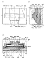
- FIG. 6A is a top view of a transistor which is one embodiment of the present invention.
- FIG. 6B is a cross-sectional view taken along the dashed-dotted line A3-A4 in FIG. That is, a cross-sectional view in the channel width direction in the channel formation region of the transistor is shown.
- FIG. 6C is a cross-sectional view taken along the dashed-dotted line A1-A2 in FIG. That is, a cross-sectional view of the transistor in the channel length direction is shown.
- some elements are omitted for clarity of illustration.
- the transistor is disposed over the insulator 401b.
- the insulator 401b is provided over the insulator 401a
- the insulator 401a is provided over the substrate 400.
- the transistor includes an insulator 301, a conductor 310, an insulator 302 over the conductor 310 and the insulator 301, an insulator 303 over the insulator 302, an insulator 402 over the insulator 303, and an insulator 402.
- the oxide 406c includes a region in contact with the top surface of the oxide 406b, the insulator 412 over the oxide 406c, and the conductor 404 including a region overlapping with the oxide 406c and the insulator 412.
- the insulator 301 has an opening, and the conductor 310 is provided in the opening.
- the oxide 406b the metal oxide 35 described in the above embodiment is used.
- a barrier film 417a1, a barrier film 417a2, an insulator 408a, an insulator 408b, and an insulator 410 are provided over the transistor.
- the conductor 404 has a function as a first gate electrode.
- the conductor 404 can have a stacked structure with a conductor having a function of suppressing permeation of oxygen. For example, an increase in electric resistance due to oxidation of the conductor 404 can be prevented by forming a conductor having a function of suppressing oxygen permeation as a lower layer.
- the insulator 412 functions as a first gate insulator.
- the conductor 416a1 and the conductor 416a2 have a function as a source electrode or a drain electrode.
- the conductors 416a1 and 416a2 can have a stacked structure with a conductor having a function of suppressing permeation of oxygen. For example, by forming a conductor having a function of suppressing permeation of oxygen as an upper layer, an increase in electrical resistance due to oxidation of the conductors 416a1 and 416a2 can be prevented. Note that the electrical resistance value of the conductor can be measured using a two-terminal method or the like.
- the barrier film 417a1 and the barrier film 417a2 have a function of suppressing permeation of impurities such as hydrogen and water and oxygen.
- the barrier film 417a1 is on the conductor 416a1 and prevents oxygen from diffusing into the conductor 416a1.
- the barrier film 417a2 is on the conductor 416a2 and prevents diffusion of oxygen into the conductor 416a2.
- FIG. 7A shows an enlarged view of the portion 100b surrounded by the alternate long and short dash line in FIG. 6B.
- FIG. 7B is an enlarged cross-sectional view of the portion 100a surrounded by the alternate long and short dash line in FIG. 7A is a cross-sectional view in the channel width direction of the transistor, and
- FIG. 7B is a cross-sectional view in the channel length direction of the transistor.
- a part of the configuration is omitted.
- the oxide 406b has a multilayer structure in which an oxide 406bn having a first band gap and an oxide 406bw having a second band gap are alternately stacked. It can be said that the structure is like a structure.
- the first band gap is smaller than the second band gap.
- the oxide 406b corresponds to the metal oxide 35 described in the above embodiment.
- the oxide 406bn having the first band gap corresponds to the layer 001 described in the above embodiment
- the oxide 406bw having the second band gap corresponds to the layer 002 described in the above embodiment. is doing.
- the oxide 406bn_1 is disposed so as to be in contact with the upper surface of the oxide 406a
- the oxide 406bw_1 is disposed so as to be in contact with the upper surface of the oxide 406bn_1.
- an oxide 406bn_2 having a first band gap, an oxide 406bw_2 having a second band gap, an oxide 406bn_3 having a first band gap, and an oxide 406bw_3 having a second band gap are sequentially stacked.
- the oxide 406bn_n having the first band gap is disposed at the top of the oxide 406b. That is, the oxide 406b has a multilayer structure of 2 ⁇ n ⁇ 1 layers (n is a natural number). n is 2 or more, preferably 3 or more and 10 or less.
- the thickness of the oxide 406bn having the first band gap has a region of 0.1 nm to 5.0 nm, preferably 0.5 nm to 2.0 nm.
- the thickness of the oxide 406 bw having the second band gap has a region of 0.1 nm to 5.0 nm, preferably a region of 0.1 nm to 3.0 nm.
- the oxide 406c is disposed so as to cover the entire oxide 406b.
- the conductor 404 functioning as a first gate electrode is disposed so as to cover the entire oxide 406b with the insulator 412 functioning as a first gate insulator interposed therebetween.
- the distance between the end portion of the conductor 416a1 and the end portion of the conductor 416a2, that is, the channel length of the transistor has a region of 10 nm to 300 nm, typically has a region of 20 nm to 180 nm. Shall.
- the width of the conductor 404 functioning as the first gate electrode has a region of 10 nm to 300 nm. Typically, the region has a region of 20 nm to 180 nm.
- indium gallium zinc oxide or an element M (the element M is Al, Ga, Si, B, Y, Ti, Fe, Ni, Ge, Zr, Mo, La, Ce, Nd, Hf, Ta, W, Mg, V, Be, or Cu).
- the element M is Al, Ga, Si, B, Y, Ti, Fe, Ni, Ge, Zr, Mo, La, Ce, Nd, Hf, Ta, W, Mg, V, Be, or Cu.
- gallium oxide, boron oxide, or the like can be used.
- the oxide 406bn having the first band gap preferably contains indium, zinc, or the like. Further, nitrogen may be included.
- indium oxide, indium zinc oxide, indium zinc oxide containing nitrogen, indium zinc nitride, indium gallium zinc oxide containing nitrogen, or the like can be used.
- gallium zinc oxide, indium gallium zinc oxide, or an element M are preferably included.
- the element M is Al, Ga, Si, B, Y, Ti, Fe, Ni, Ge, Zr, Mo, La, Ce, Nd, Hf, Ta, W, Mg, V, Be, or Cu are preferably included.
- gallium oxide, boron oxide, or the like can be used.
- the transistor can control the resistance of the oxide 406b by the potential applied to the conductor 404 functioning as the first gate electrode. That is, conduction (transistor is on) / non-conduction (transistor is off) between the conductor 416a1 and the conductor 416a2 having a function as a source electrode or a drain electrode is controlled by a potential applied to the conductor 404. can do.
- the oxide 406bn-n which is the uppermost layer of the oxide 406b, and the conductors 416a1 and 416a2 each functioning as a source electrode or a drain electrode are formed over the top surface and part of the side surfaces of the oxide 406bn-n. Touching. Each layer other than the oxide 406bn-n is in contact with part of the side surface of each layer. Therefore, the conductor 416a1, the conductor 416a2, and the layers of the oxide 406b each functioning as a source electrode or a drain electrode are electrically connected.
- the oxide 406b having a channel formation region has a structure in which an oxide 406bn having a first band gap and an oxide 406bw having a second band gap are alternately stacked. Description is made using a structure in which an oxide 406bn having one band gap is sandwiched between oxides 406bw having a second band gap.
- FIG. 15B is a band diagram in the vicinity of a conduction band lower end (hereinafter referred to as an Ec end) in a structure in which an oxide 406bn having a first band gap is sandwiched between oxides 406bw having a second band gap. Shown in A).
- the oxide 406bn having the first band gap is relatively narrower than the oxide 406bw having the second band gap, the oxide having the first band gap is oxidized.
- the Ec end of the object 406bn exists at a position relatively lower than the Ec end of the oxide 406bw having the second band gap.
- the junction between the oxide 406bn having the first band gap and the oxide 406bw having the second band gap has fluctuations in the aggregated form and composition of the oxide.
- the band is not discontinuous but continuously changes as shown in FIG.
- the oxide 406bn having the first band gap and the oxide 406bw having the second band gap interact electrically, so that the transistor is turned on.
- the oxide 406bn having a first band gap having a low Ec end serves as a main conduction path, and electrons flow. Electrons also flow through the oxide 406bw having a band gap of 2. Therefore, a high current driving capability, that is, a large on current and a high field effect mobility can be obtained in the on state of the transistor.
- the carrier density of the oxide 406bn is 6 ⁇ 10 18 cm ⁇ 3 or more and 5 ⁇ 10 20 cm ⁇ 3 or less.
- the oxide 406bn may be degenerated.
- the oxide 406 bw having the second band gap behaves as a dielectric (insulator). Therefore, the oxide 406 bw The conduction path inside is interrupted.
- the oxide 406bn having the first band gap is in contact with the oxide 406bw having the second band gap vertically.
- the oxide 406bw having the second band gap electrically interacts with the oxide 406bn having the first band gap in addition to itself, and even the conduction path in the oxide 406bn having the first band gap is obtained. Also shuts off. Thus, the entire oxide 406b is turned off, and the transistor is turned off.
- the top surface and the side surface of the oxide 406b have regions in contact with the conductor 416a1 and the conductor 416a2.
- the oxide 406c is disposed so as to cover the entire oxide 406b.
- the conductor 404 having a function of the first gate electrode is disposed so as to cover the entire oxide 406b with the insulator 412 having a function of the first gate insulator interposed therebetween. Accordingly, the entire region of the oxide 406b can be electrically surrounded by the electric field of the conductor 404 functioning as the first gate electrode.
- a transistor structure that electrically surrounds the channel formation region by an electric field of the first gate electrode is referred to as a surrounded channel (s-channel) structure. Therefore, since a channel can be formed in the entire oxide 406bn having the first band gap of the oxide 406b, a large current can be passed between the source and the drain by the above-described mechanism, and a current during conduction ( ON current) can be increased. In addition, since the entire oxide 406bw having the second band gap of the oxide 406b is surrounded by the electric field of the conductor 404, the non-conducting current (off-state current) can be reduced by the above-described mechanism. it can.
- the transistor 404 includes a region where the conductor 404 functioning as a first gate electrode overlaps with the conductors 416a1 and 416a2 functions as a source electrode or a drain electrode. And a parasitic capacitance formed by the conductor 416a1 and a parasitic capacitance formed by the conductor 404 and the conductor 416a2.
- the transistor has a structure in which a barrier film 417a1 is provided between the conductor 404 and the conductor 416a1 in addition to the insulator 412 and the oxide 406c, so that the parasitic capacitance can be reduced. it can.
- the parasitic capacitance can be reduced. Therefore, the transistor has excellent frequency characteristics.
- the transistor when the transistor has the above structure, when the transistor operates, for example, when a potential difference is generated between the conductor 404 and the conductor 416a1 or 416a2, the conductor 404 and the conductor 416a1 or Leakage current between the conductor 416a2 can be reduced or prevented.
- the conductor 310 has a function as a second gate electrode.
- the conductor 310 can be a multilayer film including a conductor having a function of suppressing permeation of oxygen. By using a multilayer film including a conductor having a function of suppressing oxygen permeation, a decrease in conductivity due to oxidation of the conductor 310 can be prevented.
- the insulator 302, the insulator 303, and the insulator 402 function as a second gate insulating film.
- the threshold voltage of the transistor can be controlled by the potential applied to the conductor 310.
- an insulator substrate, a semiconductor substrate, or a conductor substrate may be used.
- the insulator substrate include a glass substrate, a quartz substrate, a sapphire substrate, a stabilized zirconia substrate (such as a yttria stabilized zirconia substrate), and a resin substrate.
- the semiconductor substrate include a single semiconductor substrate such as silicon or germanium, or a compound semiconductor substrate made of silicon carbide, silicon germanium, gallium arsenide, indium phosphide, zinc oxide, or gallium oxide.
- there is a semiconductor substrate having an insulator region inside the semiconductor substrate for example, an SOI (Silicon On Insulator) substrate.
- the conductor substrate examples include a graphite substrate, a metal substrate, an alloy substrate, and a conductive resin substrate.
- a substrate having a metal nitride examples include a substrate having a metal oxide, and the like.
- a substrate in which a conductor or a semiconductor is provided on an insulator substrate examples include a substrate in which a conductor or an insulator is provided on a semiconductor substrate, a substrate in which a semiconductor or an insulator is provided on a conductor substrate, and the like.
- a substrate in which an element is provided may be used.
- the element provided on the substrate include a capacitor element, a resistor element, a switch element, a light emitting element, and a memory element.
- a flexible substrate may be used as the substrate 400.
- a method for providing a transistor over a flexible substrate there is a method in which after a transistor is manufactured over a non-flexible substrate, the transistor is peeled off and transferred to the substrate 400 which is a flexible substrate.
- a separation layer is preferably provided between the non-flexible substrate and the transistor.
- a sheet, a film, a foil, or the like in which fibers are knitted may be used as the substrate 400.
- the substrate 400 may have elasticity. Further, the substrate 400 may have a property of returning to the original shape when bending or pulling is stopped. Or you may have a property which does not return to an original shape.
- the substrate 400 has a region having a thickness of, for example, 5 ⁇ m to 700 ⁇ m, preferably 10 ⁇ m to 500 ⁇ m, and more preferably 15 ⁇ m to 300 ⁇ m.
- a semiconductor device including a transistor can be reduced in weight.
- the substrate 400 may have elasticity even when glass or the like is used, or may have a property of returning to its original shape when bending or pulling is stopped. Therefore, an impact applied to the semiconductor device on the substrate 400 due to a drop or the like can be reduced. That is, a durable semiconductor device can be provided.
- the substrate 400 which is a flexible substrate
- a metal, an alloy, a resin, glass, or fiber thereof can be used as the substrate 400 which is a flexible substrate.
- the substrate 400, which is a flexible substrate is preferable because the deformation due to the environment is suppressed as the linear expansion coefficient is lower.
- a material having a linear expansion coefficient of 1 ⁇ 10 ⁇ 3 / K or less, 5 ⁇ 10 ⁇ 5 / K or less, or 1 ⁇ 10 ⁇ 5 / K or less is used as the substrate 400 that is a flexible substrate.
- the resin include polyester, polyolefin, polyamide (such as nylon and aramid), polyimide, polycarbonate, and acrylic.
- aramid has a low coefficient of linear expansion, it is suitable as the substrate 400 that is a flexible substrate.
- ⁇ Insulator> electrical characteristics of the transistor can be stabilized by surrounding the transistor with an insulator having a function of suppressing permeation of impurities such as hydrogen and oxygen.
- an insulator having a function of suppressing permeation of impurities such as hydrogen and oxygen can be used as the insulator 401a, the insulator 401b, the insulator 408a, and the insulator 408b.
- Examples of the insulator having a function of suppressing permeation of impurities such as hydrogen and oxygen include boron, carbon, nitrogen, oxygen, fluorine, magnesium, aluminum, silicon, phosphorus, chlorine, argon, gallium, germanium, yttrium, and zirconium.
- An insulator containing lanthanum, neodymium, hafnium, or tantalum may be used as a single layer or a stacked layer.
- the insulator 401a, the insulator 401b, the insulator 408a, and the insulator 408b include aluminum oxide, magnesium oxide, gallium oxide, germanium oxide, yttrium oxide, zirconium oxide, lanthanum oxide, neodymium oxide, hafnium oxide, or oxide
- a metal oxide such as tantalum, silicon nitride oxide, silicon nitride, or the like may be used.
- the insulator 401a, the insulator 401b, the insulator 408a, and the insulator 408b preferably include aluminum oxide.
- oxygen can be added to the insulator 412 serving as a base layer.
- the added oxygen becomes excess oxygen in the insulator 412, and by performing heat treatment or the like, the excess oxygen passes through the insulator 412, and is added to the oxide 406a, the oxide 406b, and the oxide 406c.
- the oxygen defect in the oxide 406b, the oxide 406b, and the oxide 406c can be repaired.
- the insulator 401a, the insulator 401b, the insulator 408a, and the insulator 408b include aluminum oxide, entry of impurities such as hydrogen into the oxide 406a, the oxide 406b, and the oxide 406c can be suppressed.
- the insulator 401a, the insulator 401b, the insulator 408a, and the insulator 408b include aluminum oxide, outward diffusion of excess oxygen added to the oxide 406a, the oxide 406b, and the oxide 406c is performed. Can be reduced.
- the insulator 301, the insulator 302, the insulator 303, the insulator 402, and the insulator 412 for example, boron, carbon, nitrogen, oxygen, fluorine, magnesium, aluminum, silicon, phosphorus, chlorine, argon, gallium, germanium,
- An insulator containing yttrium, zirconium, lanthanum, neodymium, hafnium, or tantalum may be used as a single layer or a stacked layer.
- the insulator 301, the insulator 302, the insulator 303, the insulator 402, and the insulator 412 preferably include silicon oxide or silicon oxynitride.
- the insulator 302, the insulator 303, the insulator 402, and the insulator 412 preferably have an insulator with a high relative dielectric constant.
- the insulator 302, the insulator 303, the insulator 402, and the insulator 412 include gallium oxide, hafnium oxide, an oxide including aluminum and hafnium, an oxynitride including aluminum and hafnium, an oxide including silicon and hafnium, Alternatively, it preferably includes oxynitride including silicon and hafnium.
- the insulator 302, the insulator 303, the insulator 402, and the insulator 412 preferably have a stacked structure of silicon oxide or silicon oxynitride and an insulator with a high relative dielectric constant. Since silicon oxide and silicon oxynitride are thermally stable, a stacked structure having high thermal stability and high relative dielectric constant can be obtained by combining with an insulator having high relative dielectric constant. For example, when aluminum oxide, gallium oxide, or hafnium oxide is provided on the oxide 406c side, entry of silicon contained in silicon oxide or silicon oxynitride into the oxide 406b can be suppressed.
- a trap center may be formed at the interface between aluminum oxide, gallium oxide, or hafnium oxide and silicon oxide or silicon oxynitride. .
- the trap center can change the threshold voltage of the transistor in the positive direction by capturing electrons.
- the insulator 410 preferably includes an insulator having a low relative dielectric constant.
- the insulator 410 includes silicon oxide, silicon oxynitride, silicon nitride oxide, silicon nitride, silicon oxide to which fluorine is added, silicon oxide to which carbon is added, silicon oxide to which carbon and nitrogen are added, and silicon oxide having a hole Or it is preferable to have resin etc.
- the insulator 410 is formed using silicon oxide, silicon oxynitride, silicon nitride oxide, silicon nitride, silicon oxide to which fluorine is added, silicon oxide to which carbon is added, silicon oxide to which carbon and nitrogen are added, or silicon oxide having a hole And a laminated structure of resin.
- silicon oxide and silicon oxynitride are thermally stable, a laminated structure having a low thermal stability and a low relative dielectric constant can be obtained by combining with silicon.
- the resin include polyester, polyolefin, polyamide (such as nylon and aramid), polyimide, polycarbonate, and acrylic.
- an insulator having a function of suppressing permeation of impurities such as hydrogen and oxygen may be used. With the barrier films 417a1 and 417a2, excess oxygen in the insulator 410 can be prevented from diffusing into the conductors 416a1 and 416a2.
- barrier film 417a1 and the barrier film 417a2 examples include metal oxides such as aluminum oxide, magnesium oxide, gallium oxide, germanium oxide, yttrium oxide, zirconium oxide, lanthanum oxide, neodymium oxide, hafnium oxide, and tantalum oxide, and silicon nitride oxide Alternatively, silicon nitride or the like may be used. Note that the barrier film 417a1 and the barrier film 417a2 preferably include aluminum oxide.
- Conductor 404 As the conductor 404, the conductor 310, the conductor 416a1, and the conductor 416a2, aluminum, chromium, copper, silver, gold, platinum, tantalum, nickel, titanium, molybdenum, tungsten, hafnium, vanadium, niobium, manganese, magnesium, A material containing one or more metal elements selected from zirconium, beryllium, indium, and the like can be used. Alternatively, a semiconductor with high electrical conductivity typified by polycrystalline silicon containing an impurity element such as phosphorus, or silicide such as nickel silicide may be used.
- the above-described conductive material containing the metal element and oxygen may be used.
- the above-described conductive material containing a metal element and nitrogen may be used.
- a conductive material containing nitrogen such as titanium nitride or tantalum nitride may be used.
- Indium tin oxide (ITO: Indium Tin Oxide) indium oxide containing tungsten oxide, indium zinc oxide containing tungsten oxide, indium oxide containing titanium oxide, indium tin oxide containing titanium oxide, indium zinc Indium tin oxide to which oxide or silicon is added may be used.
- indium gallium zinc oxide containing nitrogen may be used.
- a plurality of conductive layers formed of the above materials may be stacked.
- a stacked structure in which the above-described material containing a metal element and a conductive material containing oxygen may be combined.
- a stacked structure in which the above-described material containing a metal element and a conductive material containing nitrogen are combined may be employed.
- a stacked structure of a combination of the above-described material containing a metal element, a conductive material containing oxygen, and a conductive material containing nitrogen may be employed.
- a stacked structure in which the above-described material containing a metal element and a conductive material containing oxygen are used as a gate electrode is preferably used.
- a conductive material containing oxygen is preferably provided on the channel formation region side.
- FIG. 8A is a top view of the transistor.
- FIG. 8B is a cross-sectional view taken along the dashed-dotted line A3-A4 in FIG. That is, a cross-sectional view in the channel width direction in the channel formation region of the transistor is shown.
- FIG. 8C is a cross-sectional view taken along the dashed-dotted line A1-A2 in FIG. That is, a cross-sectional view of the transistor in the channel length direction is shown.
- FIG. 8A some elements are omitted for clarity.
- the transistor is disposed over the insulator 401b.
- the insulator 401b is provided over the insulator 401a
- the insulator 401a is provided over the substrate 400.
- the transistor includes an insulator 301, a conductor 310, an insulator 302 over the conductor 310 and the insulator 301, an insulator 303 over the insulator 302, an insulator 402 over the insulator 303, and an insulator 402.
- a barrier film 417a1 is provided over the conductor 416a
- a barrier film 417a2 is provided over the conductor 416a2.
- An insulator 408a and an insulator 408b are provided in this order over the insulator 410, the conductor 404, the oxide 406c, and the insulator 412.
- the conductor 404 has a function as a first gate electrode.
- the conductor 404 can have a stacked structure with a conductor having a function of suppressing permeation of oxygen. For example, an increase in electric resistance due to oxidation of the conductor 404 can be prevented by forming a conductor having a function of suppressing oxygen permeation as a lower layer.
- the insulator 412 functions as a first gate insulator.
- the conductor 416a1 and the conductor 416a2 have a function as a source electrode or a drain electrode.
- the conductors 416a1 and 416a2 can have a stacked structure with a conductor having a function of suppressing permeation of oxygen. For example, by forming a conductor having a function of suppressing permeation of oxygen as an upper layer, an increase in electrical resistance due to oxidation of the conductors 416a1 and 416a2 can be prevented. Note that the electrical resistance value of the conductor can be measured using a two-terminal method or the like.
- the barrier film 417a1 and the barrier film 417a2 have a function of suppressing permeation of impurities such as hydrogen and water and oxygen.
- the barrier film 417a1 is on the conductor 416a1 and prevents oxygen from diffusing into the conductor 416a1.
- the barrier film 417a2 is on the conductor 416a2 and prevents diffusion of oxygen into the conductor 416a2.
- the region functioning as a gate electrode is formed in a self-aligned manner so as to fill the opening formed by the insulator 410 or the like, so that a TGSA s-channel FET (Trench Gate Self Aligns) is formed.
- TGSA s-channel FET Trench Gate Self Aligns
- the length of a region where the bottom surface of the conductor 404 functioning as a gate electrode faces in parallel with the top surface of the oxide 406b with the insulator 412 and the oxide 406c interposed therebetween is expressed as a gate line width. It is defined as The gate line width can be smaller than the opening reaching the oxide 406b of the insulator 410. That is, the gate line width can be made smaller than the minimum processing dimension. Specifically, the gate line width can have a region of 10 nm to 300 nm. Typically, it can have a region of 20 nm to 180 nm.
- transistor configuration 1 For other configurations and effects, refer to transistor configuration 1.
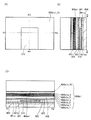
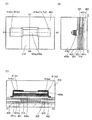
- FIGS. 6A and 6B A method for manufacturing the transistor illustrated in FIGS. 6A and 6B according to the present invention will be described below with reference to FIGS. 6 and 9 to 12, (A) in each drawing is a top view, and (B) in each drawing is a cross-sectional view corresponding to the alternate long and short dash line A1-A2 shown in (A). (C) of each figure is sectional drawing corresponding to the dashed-dotted line A3-A4 shown to (A).
- the substrate 400 is prepared.
- an insulator 401a is formed.
- the insulator 401a is formed by a sputtering method, a chemical vapor deposition (CVD) method, a molecular beam epitaxy (MBE) method, a pulsed laser deposition (PLD: Pulsed Laser Deposition) method, or an atomic layer.
- the deposition can be performed using an ALD (Atomic Layer Deposition) method or the like.
- the CVD method can be classified into a plasma CVD (PECVD: Plasma Enhanced CVD) method using plasma, a thermal CVD (TCVD: Thermal CVD) method using heat, a photo CVD (Photo CVD) method using light, and the like.
- PECVD Plasma Enhanced CVD
- TCVD Thermal CVD
- Photo CVD Photo CVD
- MCVD Metal CVD
- MOCVD Metal Organic CVD
- the plasma CVD method can obtain a high-quality film at a relatively low temperature.
- the thermal CVD method is a film formation method that can reduce plasma damage to an object to be processed because plasma is not used.
- a wiring, an electrode, an element (a transistor, a capacitor, or the like) included in the semiconductor device may be charged up by receiving electric charge from plasma.
- a wiring, an electrode, an element, or the like included in the semiconductor device may be destroyed by the accumulated charge.
- plasma damage during film formation does not occur, so that a film with few defects can be obtained.
- the ALD method is also a film forming method that can reduce plasma damage to the object to be processed.
- the ALD method does not cause plasma damage during film formation, a film with few defects can be obtained.
- the CVD method and the ALD method are film forming methods in which a film is formed by reaction on the surface of an object to be processed, unlike a film forming method in which particles emitted from a target or the like are deposited. Therefore, it is a film forming method that is not easily affected by the shape of the object to be processed and has good step coverage.
- the ALD method has excellent step coverage and excellent thickness uniformity, and thus is suitable for covering the surface of an opening having a high aspect ratio.
- the ALD method since the ALD method has a relatively low film formation rate, it may be preferable to use it in combination with another film formation method such as a CVD method with a high film formation rate.
- the composition of the obtained film can be controlled by the flow rate ratio of the source gases.
- a film having an arbitrary composition can be formed depending on the flow rate ratio of the source gases.
- a film whose composition is continuously changed can be formed by changing the flow rate ratio of the source gas while forming the film.
- an insulator 401b is formed over the insulator 401a.
- the insulator 401b can be formed by a sputtering method, a CVD method, an MBE method, a PLD method, an ALD method, or the like.
- the insulator 301 is formed over the insulator 401b.
- the insulator 301 can be formed by a sputtering method, a CVD method, an MBE method, a PLD method, an ALD method, or the like.
- a groove reaching the insulator 401b is formed in the insulator 301.
- the groove includes, for example, a hole and an opening.
- the groove may be formed by wet etching, but dry etching is preferable for fine processing.
- an insulator that functions as an etching stopper film when the insulator 301 is etched to form a groove is preferably selected.
- a silicon oxide film is used for the insulator 301 that forms the groove
- a silicon nitride film, an aluminum oxide film, or a hafnium oxide film is preferably used as the insulator 401b.
- an aluminum oxide film is formed by an ALD method as the insulator 401a, and an aluminum oxide film is formed by a sputtering method as the insulator 401b.
- the conductor to be the conductor 310 preferably includes a conductor having a function of suppressing permeation of oxygen.
- a conductor having a function of suppressing permeation of oxygen For example, tantalum nitride, tungsten nitride, titanium nitride, or the like can be used. Alternatively, a stacked film of tantalum, tungsten, titanium, molybdenum, aluminum, copper, or molybdenum tungsten alloy can be used.
- the conductor to be the conductor 310 can be formed by a sputtering method, a CVD method, an MBE method, a PLD method, an ALD method, or the like.
- tantalum nitride is formed by a sputtering method as a conductor to be the conductor 310
- titanium nitride is formed by a CVD method on the tantalum nitride
- tungsten is formed by a CVD method on the titanium nitride.
- a conductor that becomes the conductor 310 on the insulator 301 is removed by performing chemical mechanical polishing (CMP).
- CMP chemical mechanical polishing
- the insulator 302 is formed on the insulator 301 and the conductor 310.
- the insulator 302 can be formed by a sputtering method, a CVD method, an MBE method, a PLD method, an ALD method, or the like.
- an insulator 303 is formed over the insulator 302.
- the insulator 303 can be formed by a sputtering method, a CVD method, an MBE method, a PLD method, an ALD method, or the like.
- the insulator 402 is formed over the insulator 303.
- the insulator 402 can be formed by a sputtering method, a CVD method, an MBE method, a PLD method, an ALD method, or the like.
- the first heat treatment may be performed at 250 ° C to 650 ° C, preferably 450 ° C to 600 ° C, more preferably 520 ° C to 570 ° C.
- the first heat treatment is performed in an inert gas atmosphere or an atmosphere containing an oxidizing gas at 10 ppm or more, 1% or more, or 10% or more.
- the first heat treatment may be performed in a reduced pressure state.
- the first heat treatment may be performed in an atmosphere containing an oxidizing gas of 10 ppm or more, 1% or more, or 10% or more to supplement the desorbed oxygen after the heat treatment in an inert gas atmosphere. Good.
- the first heat treatment impurities such as hydrogen and water contained in the insulator 402 can be removed.
- plasma treatment containing oxygen may be performed in a reduced pressure state.
- the plasma treatment including oxygen it is preferable to use an apparatus having a power source that generates high-density plasma using microwaves, for example.
- a power source for applying RF (Radio Frequency) may be provided on the substrate side.
- High-density oxygen radicals can be generated by using high-density plasma, and oxygen radicals generated by high-density plasma can be efficiently guided into the insulator 402 by applying RF to the substrate side.
- plasma treatment containing oxygen may be performed to supplement oxygen that has been desorbed after performing plasma treatment containing an inert gas using this apparatus. Note that the first heat treatment may not be performed.
- an oxide 406 a 1 is formed over the insulator 402.
- the oxide 406a1 can be formed by a sputtering method, a CVD method, an MBE method, a PLD method, an ALD method, or the like.
- treatment for adding oxygen to the oxide 406a1 may be performed.
- the treatment for adding oxygen include an ion implantation method and a plasma treatment method. Note that oxygen added to the oxide 406a1 becomes excess oxygen.
- an oxide 406b1 is formed over the oxide 406a1 (see FIGS. 9A to 9C).
- the oxide 406b1 is preferably formed by a sputtering method.
- the thickness of the oxide 406b1n having the first band gap and the thickness of the oxide 406b1w having the second band gap are set to 1 nm, and ten layers of the oxide 406b1n having the first band gap are formed.
- Form a film. Therefore, the oxide 406b1 is a stacked film of 19 layers, and the total film thickness is 19 nm. Note that the description in Embodiment 1 can be referred to for a method for forming the oxide 406b1.
- the first heat treatment condition can be used for the heat treatment.
- the second heat treatment is preferably performed in a nitrogen atmosphere at a temperature of 400 ° C. for 1 hour and then continuously in an oxygen atmosphere at a temperature of 400 ° C. for 1 hour.
- a resist mask is formed over the oxide 406b1 by a lithography method, and the oxide 406b1 and the oxide 406a1 are etched.
- the oxide 406b1 and the oxide 406a1 can be etched by a dry etching method.
- the oxide 406b1 has a multilayer structure in which oxides having a first band gap and oxides having a second band gap are alternately stacked.
- a dry etching apparatus in which the etching conditions for the oxide having the first band gap and the etching conditions for the oxide having the second band gap can be appropriately switched according to the stacked structure is used. preferable. In some cases, the oxide having the first band gap and the oxide having the second band gap can be etched under the same conditions.
- the oxide 406a1 is etched to form the oxide 406b and the oxide 406a (see FIGS. 10A to 10C).
- a resist is exposed through a mask.
- a resist mask is formed by removing or leaving the exposed region using a developer.
- a conductor, a semiconductor, an insulator, or the like can be processed into a desired shape by etching through the resist mask.
- the resist mask may be formed by exposing the resist using KrF excimer laser light, ArF excimer laser light, EUV (Extreme Ultraviolet) light, or the like.
- an immersion technique may be used in which exposure is performed by filling a liquid (for example, water) between the substrate and the projection lens.
- an electron beam or an ion beam may be used.
- a mask is not necessary when an electron beam or an ion beam is used.
- the resist mask can be removed by performing a dry etching process such as ashing, performing a wet etching process, performing a wet etching process after the dry etching process, or performing a dry etching process after the wet etching process.
- a capacitively coupled plasma (CCP) etching apparatus having parallel plate electrodes can be used as the dry etching apparatus.
- the capacitively coupled plasma etching apparatus having parallel plate electrodes may be configured to apply a high frequency power source to one of the parallel plate electrodes.
- a configuration in which a plurality of different high-frequency power sources are applied to one electrode of the parallel plate electrode may be employed.
- mold electrode may be sufficient.
- mold electrode may be sufficient.
- a dry etching apparatus having a high-density plasma source can be used.
- an inductively coupled plasma (ICP) etching apparatus can be used as the dry etching apparatus having a high-density plasma source.
- a conductor to be a conductor 416a1 and a conductor 416a2 is formed over the oxide 406b1.
- the conductors to be the conductors 416a1 and 416a2 can be formed by a sputtering method, a CVD method, an MBE method, a PLD method, an ALD method, or the like.
- a conductive oxide for example, indium tin oxide (ITO), indium oxide containing tungsten oxide, indium zinc oxide containing tungsten oxide
- ITO indium tin oxide
- a film of indium oxide containing titanium oxide, indium tin oxide containing titanium oxide, indium zinc oxide, indium tin oxide added with silicon, or indium gallium zinc oxide containing nitrogen is formed on the oxide;
- one or more metal elements selected from aluminum, chromium, copper, silver, gold, platinum, tantalum, nickel, titanium, molybdenum, tungsten, hafnium, vanadium, niobium, manganese, magnesium, zirconium, beryllium, indium, etc.
- Materials, including Is typified by polycrystalline silicon which contains an impurity element such as phosphorus, high electric conductivity semiconductor film may be formed a silicide such as nickel silicide.
- the oxide may have a function of absorbing hydrogen in the oxide 406a and the oxide 406b and capturing hydrogen diffused from the outside, which may improve electrical characteristics and reliability of the transistor.
- the same function may be obtained even when titanium is used instead of the oxide.
- barrier films to be the barrier films 417a1 and 417a2 are formed over the conductors to be the conductors 416a1 and 416a2.
- the barrier films to be the barrier films 417a1 and 417a2 can be formed by a sputtering method, a CVD method, an MBE method, a PLD method, an ALD method, or the like.
- aluminum oxide is formed as a barrier film to be the barrier film 417a1 and the barrier film 417a2.
- a conductor 416a1, a conductor 416a2, a barrier film 417a1, and a barrier film 417a2 are formed by a lithography method. (See FIGS. 11A to 11C.)
- a cleaning treatment may be performed using an aqueous solution (diluted hydrofluoric acid solution) obtained by diluting hydrofluoric acid with pure water.
- the diluted hydrofluoric acid solution is a solution in which hydrofluoric acid is mixed with pure water at a concentration of about 70 ppm.
- a third heat treatment is performed.
- the first heat treatment condition described above can be used as the heat treatment condition.
- the treatment is continuously performed for 1 hour at a temperature of 400 ° C. in an oxygen atmosphere.
- impurities due to the etching gas may adhere or diffuse on the surface or inside of the oxide 406a and the oxide 406b.
- impurities include fluorine and chlorine.
- the impurity concentration can be reduced by performing the above-described treatment. Further, the moisture concentration and the hydrogen concentration in the oxide 406a film and the oxide 406b film can be reduced.
- the oxide film to be the oxide 406c can be formed by a sputtering method, a CVD method, an MBE method, a PLD method, an ALD method, or the like. In particular, it is preferable to form a film using a sputtering method.
- a mixed gas of oxygen and argon is used, preferably a condition having a high oxygen partial pressure, more preferably a condition using 100% oxygen, and a temperature of room temperature or 100 ° C. to 200 ° C. The film is formed.
- an oxide to be the oxide 406c under the above conditions so that excess oxygen can be injected into the oxide 406a, the oxide 406b, and the insulator 402.
- an insulator to be the insulator 412 is formed over the oxide to be the oxide 406c.
- the insulator to be the insulator 412 can be formed by a sputtering method, a CVD method, an MBE method, a PLD method, an ALD method, or the like.
- the fourth heat treatment can be performed.
- the first heat treatment condition can be used for the heat treatment.
- the treatment is continuously performed for 1 hour at a temperature of 400 ° C. in an oxygen atmosphere.
- the conductor to be the conductor 404 can be formed by a sputtering method, a CVD method, an MBE method, a PLD method, an ALD method, or the like.
- the conductor to be the conductor 404 may be a multilayer film.
- oxygen can be added to the insulator to be the insulator 412 by forming an oxide film under the same conditions as the oxide to be the oxide 406c.
- the oxygen added to the insulator to be the insulator 412 becomes excess oxygen.
- the electrical resistance value of the oxide can be lowered by forming a conductor on the oxide by a sputtering method.
- a conductor to be the conductor 404 is processed by a lithography method to form the conductor 404.
- the oxide to be the oxide 406c and the insulator to be the insulator 412 are processed by a lithography method to form the oxide 406c and the insulator 412 (see FIGS. 12A to 12C). Note that although an example in which the oxide 406c and the insulator 412 are formed after the conductor 404 is formed is described in this embodiment, the conductor 404 is formed after the oxide 406c and the insulator 412 are formed. It doesn't matter.
- the insulator 408a is formed, and the insulator 408b is formed over the insulator 408a.
- the insulator 408a and the insulator 408b can be formed by a sputtering method, a CVD method, an MBE method, a PLD method, an ALD method, or the like.
- As the insulator 408b an aluminum oxide film formed using an ALD method is formed, so that there are few pinholes and the film thickness can be uniformly formed on the top and side surfaces of the insulator 408a. Can be prevented.
- the insulator 410 is formed over the insulator 408b.
- the insulator 410 can be formed by a sputtering method, a CVD method, an MBE method, a PLD method, an ALD method, or the like.
- a spin coating method, a dip method, a droplet discharge method (such as an ink jet method), a printing method (such as screen printing or offset printing), a doctor knife method, a roll coater method, or a curtain coater method can be used.
- the insulator 410 is preferably formed by a CVD method. More preferably, the film is formed using a plasma CVD method. In film formation by the plasma CVD method, step 1 for forming an insulator and step 2 for performing plasma treatment with oxygen may be repeated. By repeating Step 1 and Step 2 a plurality of times, the insulator 410 containing excess oxygen can be formed.
- the insulator 410 may be formed so that the upper surface has flatness.
- the insulator 410 may have a flat upper surface immediately after film formation.
- the insulator 410 may have flatness by removing the insulator and the like from the upper surface so as to be parallel to a reference surface such as the back surface of the substrate after film formation. Such a process is called a flattening process.
- the planarization process include a CMP process and a dry etching process.
- the upper surface of the insulator 410 may not have flatness.
- the first heat treatment condition can be used for the heat treatment.
- the treatment is continuously performed for 1 hour at a temperature of 400 ° C. in an oxygen atmosphere.
- the moisture concentration and the hydrogen concentration in the insulator 410 can be reduced.
- FIGS. 1-10 An example of a memory device using the semiconductor device which is one embodiment of the present invention is illustrated in FIGS.
- the memory device illustrated in FIGS. 13 and 14 includes a transistor 900, a transistor 800, a transistor 700, and a capacitor 600.
- the transistor 700 is a transistor similar to that described in FIG. 13 and 14, the insulator 712 is the insulator 401a, the insulator 714 is the insulator 401b, the insulator 716 is the insulator 301, the insulator 720 is the insulator 302, and the insulator 722 is the insulator 722.
- the insulator 303 corresponds to the insulator 402
- the insulator 772 corresponds to the insulator 408a
- the insulator 774 corresponds to the insulator 408b
- the insulator 780 corresponds to the insulator 410.
- the transistor 700 is a transistor in which a channel is formed in a semiconductor layer including an oxide semiconductor. Since the transistor 700 has a small off-state current, stored data can be held for a long time by using the transistor 700 for a memory device. That is, the refresh operation is not required or the frequency of the refresh operation is extremely low, so that the power consumption of the storage device can be sufficiently reduced.
- the off-state current of the transistor 700 can be further reduced.
- the structure in which the back gate voltage of the transistor 700 can be maintained makes it possible to hold data for a long time without supplying power.
- the transistor 900 is formed in the same layer as the transistor 700 and can be manufactured in parallel.
- the insulator 716 and the insulator 716 have an opening, and the conductor 310a, the conductor 310b, and the conductor 310c are provided in the opening, and the conductor 310a, the conductor 310b, and the conductor 310c are arranged.
- the conductor 310a, the conductor 310b, and the conductor 310c are the same layer as the conductor 310
- the oxide 406d is the same layer as the oxide 406c
- the insulator 412a is the same layer as the insulator 412
- the conductor 404a Is formed of the same layer as the conductor 404.
- the conductor 310a and the conductor 310c are in contact with the oxide 406d through openings formed in the insulators 720, 722, and 724.
- the conductor 310a or the conductor 310c can function as either a source electrode or a drain electrode.
- One of the conductor 404a and the conductor 310b can function as a gate electrode, and the other can function as a back gate electrode.
- the threshold voltage of the transistor 900 can be made higher than 0 V, the off current can be reduced, and Icut can be made extremely small.
- Icut refers to the drain current when the back gate voltage and the top gate voltage are 0V.
- the back gate voltage of the transistor 700 is controlled by the transistor 900.
- the top gate and the back gate of the transistor 900 are diode-connected to the source, and the source of the transistor 900 and the back gate of the transistor 700 are connected to each other.
- the voltage between the top gate and the source of the transistor 900 and the voltage between the back gate and the source are 0V. Since Icut of the transistor 900 is very small, by using this structure, the negative potential of the back gate of the transistor 700 can be maintained for a long time without supplying power to the transistor 700 and the transistor 900.
- the memory device including the transistor 700 and the transistor 900 can hold stored data for a long time.
- the wiring 3001 is electrically connected to the source of the transistor 800, and the wiring 3002 is electrically connected to the drain of the transistor 800.
- the wiring 3003 is electrically connected to one of a source and a drain of the transistor 700, the wiring 3004 is electrically connected to the gate of the transistor 700, and the wiring 3006 is electrically connected to the back gate of the transistor 700.
- the gate of the transistor 800 and the other of the source and the drain of the transistor 700 are electrically connected to one of the electrodes of the capacitor 600, and the wiring 3005 is electrically connected to the other of the electrodes of the capacitor 600. .
- the wiring 3007 is electrically connected to the source of the transistor 900
- the wiring 3008 is electrically connected to the gate of the transistor 900
- the wiring 3009 is electrically connected to the back gate of the transistor 900
- the wiring 3010 is connected to the drain of the transistor 900. And are electrically connected.
- the wiring 3006, the wiring 3007, the wiring 3008, and the wiring 3009 are electrically connected.
- the memory device illustrated in FIGS. 13 and 14 has a characteristic that the potential of the gate of the transistor 800 can be held, so that information can be written, held, and read as described below.
- the potential of the wiring 3004 is set to a potential at which the transistor 700 is turned on, so that the transistor 700 is turned on. Accordingly, the potential of the wiring 3003 is supplied to the node FG that is electrically connected to one of the gate of the transistor 800 and the electrode of the capacitor 600. That is, predetermined charge is given to the gate of the transistor 800 (writing).
- predetermined charge is given to the gate of the transistor 800 (writing).
- the potential of the wiring 3004 is set to a potential at which the transistor 700 is turned off and the transistor 700 is turned off, whereby charge is held at the node FG (holding).
- the wiring 3002 takes a potential corresponding to the amount of charge held in the node FG.
- the apparent threshold voltage V th_H in the case where a high level charge is applied to the gate of the transistor 800 is a low level charge applied to the gate of the transistor 800.
- the apparent threshold voltage refers to the potential of the wiring 3005 necessary for bringing the transistor 800 into a “conductive state”.
- the potential of the wiring 3005 when the potential of the wiring 3005 is set to the potential V 0 between V th_H and V th_L , the charge given to the node FG can be determined. For example, in writing, when a high-level charge is applied to the node FG, the transistor 800 is turned “on” when the potential of the wiring 3005 is V 0 (> V th_H ). On the other hand, in the case where a low-level charge is supplied to the node FG, the transistor 800 remains in a “non-conduction state” even when the potential of the wiring 3005 becomes V 0 ( ⁇ V th_L ). Therefore, by determining the potential of the wiring 3002, information held in the node FG can be read.
- a memory cell array can be configured by arranging the storage devices shown in FIGS. 13 and 14 in a matrix.
- the memory device illustrated in FIGS. 13 and 14 may not have the transistor 800. Even in the case where the transistor 800 is not provided, information writing and holding operations can be performed by operations similar to those of the memory device described above.
- the charge is The potential of the wiring 3003 after the redistribution is (CB ⁇ VB0 + CV) / (CB + C).
- the potential of one of the electrodes of the capacitor 600 takes two states of V1 and V0 (V1> V0) as the state of the memory cell
- information can be read by comparing the potential of the wiring 3003 with a predetermined potential.
- a transistor to which silicon is applied is used for a driver circuit for driving a memory cell, and a transistor to which an oxide semiconductor is applied is stacked over the driver circuit as the transistor 700. And it is sufficient.
- the memory device described above can hold stored data for a long time by using a transistor with an off-state current that uses an oxide semiconductor. That is, a refresh operation is not necessary or the frequency of the refresh operation can be extremely low, so that a memory device with low power consumption can be realized.
- stored data can be held for a long time even when power is not supplied (note that a potential is preferably fixed).
- the storage device does not require a high voltage for writing information, the element hardly deteriorates.
- the memory device unlike the conventional nonvolatile memory, since electrons are not injected into the floating gate and electrons are not extracted from the floating gate, there is no problem of deterioration of the insulator. That is, the memory device according to one embodiment of the present invention is a memory device in which the number of rewritable times is not limited and the reliability is drastically improved unlike a conventional nonvolatile memory. Further, since data is written depending on the conductive state and non-conductive state of the transistor, high-speed operation is possible.
- the transistor 700 uses an oxide having a multilayer structure as an active layer, so that a large on-state current can be obtained. As a result, the information writing speed is further improved, and high-speed operation becomes possible.
- FIG. 1 An example of a memory device of one embodiment of the present invention is illustrated in FIG.
- the memory device includes a transistor 900, a transistor 800, a transistor 700, and a capacitor 600.
- the transistor 700 is provided above the transistor 800
- the capacitor 600 is provided above the transistor 800 and the transistor 700.
- the transistor 800 is provided over a substrate 811, and includes a conductor 816, an insulator 814, a semiconductor region 812 including a part of the substrate 811, a low resistance region 818 a functioning as a source region or a drain region, and a low resistance region 818 b. Have.
- the transistor 800 may be either a p-channel type or an n-channel type.
- a region where a channel of the semiconductor region 812 is formed, a region in the vicinity thereof, a low resistance region 818a which serves as a source region or a drain region, a low resistance region 818b, and the like preferably include a semiconductor such as a silicon-based semiconductor. It preferably contains crystalline silicon. Alternatively, a material containing Ge (germanium), SiGe (silicon germanium), GaAs (gallium arsenide), GaAlAs (gallium aluminum arsenide), or the like may be used. A structure using silicon in which effective mass is controlled by applying stress to the crystal lattice and changing the lattice spacing may be employed. Alternatively, the transistor 800 may be a HEMT (High Electron Mobility Transistor) by using GaAs, GaAlAs, or the like.
- HEMT High Electron Mobility Transistor
- the low-resistance region 818a and the low-resistance region 818b provide an n-type conductivity element such as arsenic or phosphorus, or a p-type conductivity property such as boron, in addition to the semiconductor material used for the semiconductor region 812. Containing elements.
- the conductor 816 functioning as a gate electrode includes a semiconductor material such as silicon, a metal material, an alloy containing an element imparting n-type conductivity such as arsenic or phosphorus, or an element imparting p-type conductivity such as boron.
- a conductive material such as a material or a metal oxide material can be used.
- the threshold voltage can be adjusted by determining the work function depending on the material of the conductor. Specifically, it is preferable to use a material such as titanium nitride or tantalum nitride for the conductor. Further, in order to achieve both conductivity and embeddability, it is preferable to use a metal material such as tungsten or aluminum as a laminate for the conductor, and tungsten is particularly preferable from the viewpoint of heat resistance.
- the transistor 800 illustrated in FIGS. 1A and 1B is an example and is not limited to the structure, and an appropriate transistor may be used depending on a circuit configuration or a driving method. In the case of the structure described in ⁇ Structure 2 of storage device>, the transistor 800 is not necessarily provided.
- An insulator 820, an insulator 822, an insulator 824, and an insulator 826 are stacked in this order so as to cover the transistor 800.
- the insulator 820, the insulator 822, the insulator 824, and the insulator 826 for example, silicon oxide, silicon oxynitride, silicon nitride oxide, silicon nitride, aluminum oxide, aluminum oxynitride, aluminum nitride oxide, aluminum nitride, or the like is used. That's fine.
- the insulator 822 may function as a planarization film that planarizes a step generated by the transistor 800 or the like provided below the insulator 822.
- the top surface of the insulator 822 may be planarized by a planarization process using a CMP method or the like to improve planarity.
- the insulator 824 is preferably formed using a film having a barrier property such that hydrogen and impurities do not diffuse from the substrate 811 or the transistor 800 to a region where the transistor 700 and the transistor 900 are provided.
- the barrier property is a function of suppressing diffusion of impurities typified by hydrogen and water.
- the diffusion distance of hydrogen per hour in a film having a barrier property may be 50 nm or less in an atmosphere of 350 ° C. or 400 ° C.
- the diffusion distance of hydrogen per hour in the film having a barrier property in an atmosphere of 350 ° C. or 400 ° C. is 30 nm or less, more preferably 20 nm or less.
- a film having a barrier property against hydrogen for example, silicon nitride formed by a CVD method can be used.
- silicon nitride formed by a CVD method when hydrogen diffuses into a semiconductor element including an oxide semiconductor such as the transistor 700, characteristics of the semiconductor element may be reduced. Therefore, a film for suppressing hydrogen diffusion is preferably used between the transistor 700 and the transistor 900 and the transistor 800.
- the film that suppresses the diffusion of hydrogen is a film with a small amount of hydrogen desorption.
- the amount of hydrogen desorption can be analyzed using, for example, TDS.
- the amount of hydrogen desorbed from the insulator 824 is 2 ⁇ 10 in terms of the amount of desorption converted into hydrogen molecules in the range of 50 ° C. to 500 ° C. in terms of TDS analysis. It may be 15 molecules / cm 2 or less, preferably 1 ⁇ 10 15 molecules / cm 2 or less, more preferably 5 ⁇ 10 14 molecules / cm 2 or less.
- the insulator 826 preferably has a lower dielectric constant than the insulator 824.
- the dielectric constant of the insulator 826 is preferably less than 4, and more preferably less than 3.
- the relative dielectric constant of the insulator 824 is preferably equal to or less than 0.7 times that of the insulator 826, and more preferably equal to or less than 0.6 times.
- the insulator 820, the insulator 822, the insulator 824, and the insulator 826 are embedded with a conductor 828 that is electrically connected to the capacitor 600 or the transistor 700, a conductor 830, and the like.
- the conductor 828 and the conductor 830 function as plugs or wirings.
- a conductor having a function as a plug or a wiring may be given the same reference numeral by collecting a plurality of structures.
- the wiring and the plug electrically connected to the wiring may be integrated. That is, a part of the conductor may function as a wiring, and a part of the conductor may function as a plug.
- a conductive material such as a metal material, an alloy material, a metal nitride material, or a metal oxide material is formed in a single layer or stacked layers.
- a high melting point material such as tungsten or molybdenum that has both heat resistance and conductivity, and it is preferable to use tungsten.
- a low-resistance conductive material such as aluminum or copper. Wiring resistance can be lowered by using a low-resistance conductive material.
- a wiring layer may be provided over the insulator 826 and the conductor 830.
- an insulator 850, an insulator 852, and an insulator 854 are sequentially stacked.
- the insulator 850, the insulator 852, and the insulator 854 are formed with a conductor 856.
- the conductor 856 functions as a plug or a wiring. Note that the conductor 856 can be provided using a material similar to that of the conductor 828 and the conductor 830.
- an insulator having a barrier property against hydrogen is preferably used as the insulator 850.
- the conductor 856 preferably includes a conductor having a barrier property against hydrogen.
- a conductor having a barrier property against hydrogen is formed in an opening portion of the insulator 850 having a barrier property against hydrogen.
- tantalum nitride may be used as the conductor having a barrier property against hydrogen. Further, by stacking tantalum nitride and tungsten having high conductivity, diffusion of hydrogen from the transistor 800 can be suppressed while maintaining conductivity as a wiring. In this case, it is preferable that the tantalum nitride layer having a barrier property against hydrogen be in contact with the insulator 850 having a barrier property against hydrogen.
- An insulator 858, an insulator 710, an insulator 712, an insulator 714, and an insulator 716 are sequentially stacked over the insulator 854. Any of the insulator 858, the insulator 710, the insulator 712, the insulator 714, and the insulator 716 is preferably formed using a substance having a barrier property against oxygen or hydrogen.
- the insulator 858, the insulator 712, and the insulator 714 include barriers that prevent diffusion of hydrogen and impurities from the region where the substrate 811 or the transistor 800 is provided to the region where the transistor 700 and the transistor 900 are provided. It is preferable to use a film having a property. Therefore, a material similar to that of the insulator 824 can be used.
- silicon nitride formed by a CVD method can be used as an example of a film having a barrier property against hydrogen.
- silicon nitride formed by a CVD method when hydrogen diffuses into a semiconductor element including an oxide semiconductor such as the transistor 700, characteristics of the semiconductor element may be reduced. Therefore, a film for suppressing hydrogen diffusion is preferably used between the transistor 700 and the transistor 900 and the transistor 800.
- the film that suppresses the diffusion of hydrogen is a film with a small amount of hydrogen desorption.
- a metal oxide such as aluminum oxide, hafnium oxide, or tantalum oxide is preferably used for the insulator 712 and the insulator 714.
- aluminum oxide has a high blocking effect that prevents the film from permeating both oxygen and impurities such as hydrogen and moisture that cause fluctuations in the electrical characteristics of the transistor. Therefore, aluminum oxide can prevent impurities such as hydrogen and moisture from entering the transistor 700 and the transistor 900 during and after the manufacturing process of the transistor. In addition, release of oxygen from the oxide included in the transistor 700 can be suppressed. Therefore, the transistor 700 and the transistor 900 are suitable for use as a protective film.
- the insulator 710 and the insulator 716 can be formed using the same material as the insulator 820.
- a material having a relatively low dielectric constant for the insulating film as an interlayer film, parasitic capacitance generated between wirings can be reduced.
- a silicon oxide film, a silicon oxynitride film, or the like can be used as the insulator 716.
- the insulator 858, the insulator 710, the insulator 712, the insulator 714, and the insulator 716 include a conductor 718 and a conductor included in the transistor 700 and the transistor 900 (the conductor 705, the conductor 405, and the conductor The body 403, the conductor 407) and the like are embedded.
- the conductor 718 functions as a plug or a wiring electrically connected to the capacitor 600 or the transistor 800.
- the conductor 718 can be provided using a material similar to that of the conductor 828 and the conductor 830.
- the insulator 858, the insulator 712, and the conductor 718 in a region in contact with the insulator 714 are preferably conductors having a barrier property against oxygen, hydrogen, and water.
- the transistor 800 and the transistor 700 are layers having a barrier property against oxygen, hydrogen, and water and can be completely separated from each other, so that diffusion of hydrogen from the transistor 800 to the transistor 700 and the transistor 900 is suppressed. be able to.
- a transistor 700 and a transistor 900 are provided above the insulator 716.
- An insulator 782 and an insulator 784 are provided above the transistor 700 and the transistor 900.
- the insulator 782 and the insulator 784 can be formed using a material similar to that of the insulator 214 and the insulator 212. Accordingly, the insulator 782 and the insulator 784 function as protective films for the transistor 700 and the transistor 900.
- openings be formed in the insulators 716, 720, 722, 724, 772, 774, and 780 so that the insulator 714 and the insulator 782 are in contact with each other. With such a structure, the transistor 700 and the transistor 900 can be sealed with the insulator 714 and the insulator 782, and intrusion of impurities such as hydrogen or water can be prevented.
- An insulator 610 is provided on the insulator 784.
- the insulator 610 can be formed using a material similar to that of the insulator 820.
- a material having a relatively low dielectric constant for the insulating film as an interlayer film, parasitic capacitance generated between wirings can be reduced.
- a silicon oxide film, a silicon oxynitride film, or the like can be used as the insulator 610.
- a conductor 785 or the like is embedded in the insulator 720, the insulator 722, the insulator 724, the insulator 772, the insulator 774, and the insulator 610.
- the conductor 785 functions as a plug or a wiring electrically connected to the capacitor 600, the transistor 700, or the transistor 800.
- the conductor 785 can be provided using a material similar to that of the conductor 828 and the conductor 830.
- the conductor 785 in the case where the conductor 785 is provided as a stacked structure, it is preferable to include a conductor that is not easily oxidized (highly resistant to oxidation).
- a conductor having high oxidation resistance is preferably provided in a region in contact with the insulator 724 having an excess oxygen region. With this structure, the conductor 785 can suppress absorption of excess oxygen from the insulator 724.
- the conductor 785 preferably includes a conductor having a barrier property against hydrogen.
- impurities in the conductor 785 and part of the conductor 785 are diffused or externally It can be suppressed that it becomes a diffusion path of impurities from.
- the conductor 787, the capacitor 600, and the like are provided over the insulator 610 and the conductor 785.
- the capacitor 600 includes a conductor 612, an insulator 630, an insulator 632, an insulator 634, and a conductor 616.
- the conductor 612 and the conductor 616 function as electrodes of the capacitor 600, and the insulator 630, the insulator 632, and the insulator 634 function as dielectrics of the capacitor 600.
- the conductor 787 functions as a plug or a wiring electrically connected to the capacitor 600, the transistor 700, or the transistor 800.
- the conductor 612 functions as one of the electrodes of the capacitor 600. Note that the conductor 787 and the conductor 612 can be formed at the same time.
- the conductor 787 and the conductor 612 include a metal film containing an element selected from molybdenum, titanium, tantalum, tungsten, aluminum, copper, chromium, neodymium, and scandium, or a metal nitride film containing the above-described element as a component.
- a metal film containing an element selected from molybdenum, titanium, tantalum, tungsten, aluminum, copper, chromium, neodymium, and scandium or a metal nitride film containing the above-described element as a component.
- titanium nitride film, molybdenum nitride film, tungsten nitride film or the like can be used.
- indium tin oxide indium oxide containing tungsten oxide, indium zinc oxide containing tungsten oxide, indium oxide containing titanium oxide, indium tin oxide containing titanium oxide, indium zinc oxide, silicon oxide added It is also possible to apply a conductive material such as indium tin oxide.
- the insulator 630, the insulator 632, and the insulator 634 include, for example, silicon oxide, silicon oxynitride, silicon nitride oxide, silicon nitride, aluminum oxide, aluminum oxynitride, aluminum nitride oxide, aluminum nitride, hafnium oxide, hafnium oxynitride, Nitride hafnium oxide, hafnium nitride, or the like may be used, and a stacked layer or a single layer can be used.
- the capacitor 600 can increase the capacitance per unit area.
- the insulator 630 and the insulator 634 may be formed using a material having high dielectric strength such as silicon oxynitride. By sandwiching a high dielectric with an insulator having a high dielectric strength, electrostatic breakdown of the capacitor 600 can be suppressed and a capacitor having a large capacitance can be obtained.
- the conductor 616 is provided so as to cover a side surface and an upper surface of the conductor 612 with the insulator 630, the insulator 632, and the insulator 634 interposed therebetween.
- the side surface of the conductor 612 is surrounded by the conductor 616 with an insulator interposed therebetween.
- a capacitor is formed also on the side surface of the conductor 612, so that the capacitance per projected area of the capacitor can be increased. Accordingly, the memory device can be reduced in area, highly integrated, and miniaturized.
- the conductor 616 can be formed using a conductive material such as a metal material, an alloy material, or a metal oxide material. It is preferable to use a high-melting-point material such as tungsten or molybdenum that has both heat resistance and conductivity, and it is particularly preferable to use tungsten. In the case of forming simultaneously with other structures such as a conductor, Cu (copper), Al (aluminum), or the like, which is a low resistance metal material, may be used.
- An insulator 650 is provided over the conductor 616 and the insulator 634.
- the insulator 650 can be provided using a material similar to that of the insulator 820.
- the insulator 650 may function as a planarization film that covers the concave and convex shapes below the insulator 650.
- FIG. 14 differs from FIG. 13 in the structure of the transistor 800, the shapes of the insulator 772, the insulator 774, and the like.
- a semiconductor region 812 (a part of the substrate 811) where a channel is formed has a convex shape.
- a conductor 816 is provided so as to cover a side surface and an upper surface of the semiconductor region 812 with an insulator 814 interposed therebetween.
- the conductor 816 may be formed using a material that adjusts a work function.
- Such a transistor 800 is also called a FIN-type transistor because it uses a convex portion of a semiconductor substrate.
- an insulator functioning as a mask for forming the convex portion may be provided in contact with the upper portion of the convex portion.
- the area can be reduced, the integration can be increased, and the size can be reduced.
- a transistor including an oxide semiconductor in a memory device using a transistor including an oxide semiconductor, variation in electrical characteristics can be suppressed and reliability can be improved.
- a transistor including an oxide semiconductor with high on-state current can be provided.
- a transistor including an oxide semiconductor with low off-state current can be provided.
- a memory device with reduced power consumption can be provided.
Landscapes
- Chemical & Material Sciences (AREA)
- Chemical Kinetics & Catalysis (AREA)
- Engineering & Computer Science (AREA)
- Materials Engineering (AREA)
- Mechanical Engineering (AREA)
- Metallurgy (AREA)
- Organic Chemistry (AREA)
- Thin Film Transistor (AREA)
Abstract
新規な金属酸化物および新規なトランジスタを提供する。 第1のスパッタリングターゲットと、 第2のスパッタリングターゲットと、 シャッタと、 基板ホルダと、 を有し、 第1のスパッタリングターゲットは、 導電性材料を含み、 第2のスパッタリングターゲットは、 絶縁性材料を含み、 シャッタは、 第1のスパッタリングターゲット及び第2のスパッタリングターゲットと、基板ホルダの間に位置し、シャッタは、切欠き部が設けられ、基板ホルダは、シャッタの切欠き部を介して、第1のスパッタリングターゲットまたは第2のスパッタリングターゲットと対向される、 ことを特徴とするスパッタリング装置を用いて金属酸化物膜を成膜する。 また、 該金属酸化物膜をチャネル形成領域として用いるトランジスタ。
Description
本発明は、物、方法、または、製造方法に関する。または、本発明は、プロセス、マシン、マニュファクチャ、または、組成物(コンポジション・オブ・マター)に関する。特に、本発明の一態様は、金属酸化物、金属酸化物の製造装置または当該金属酸化物の製造方法に関する。または、本発明の一態様は、半導体装置、表示装置、液晶表示装置、発光装置、蓄電装置、記憶装置、それらの駆動方法、または、それらの製造方法に関する。
なお、本明細書等において、半導体装置とは、半導体特性を利用することで機能しうる装置全般を指す。トランジスタなどの半導体素子をはじめ、半導体回路、演算装置、記憶装置は、半導体装置の一態様である。撮像装置、表示装置、液晶表示装置、発光装置、電気光学装置、発電装置(薄膜太陽電池、有機薄膜太陽電池等を含む)、及び電子機器は、半導体装置を有している場合がある。
トランジスタに適用可能な半導体材料として、酸化物半導体が注目されている。例えば、特許文献1では、複数の酸化物半導体層を積層し、当該複数の酸化物半導体層の中で、チャネルとなる酸化物半導体層がインジウム及びガリウムを含み、且つインジウムの割合をガリウムの割合よりも大きくすることで、電界効果移動度(単に移動度、またはμFEという場合がある)を高めた半導体装置が検討されている。
また、非特許文献1では、トランジスタの活性層として、In−Zn酸化物と、In−Ga−Zn酸化物との2層積層の酸化物半導体を有する構造が検討されている。
また、非特許文献2では、トランジスタの活性層として、金属酸化物を用い、当該金属酸化物がX−O−Y構造を有する構成について検討されている。
John F.Wager、「Oxide TFTs:A Progress Report」、Information Display 1/16、SID 2016、 Jan/Feb 2016、Vol.32,No.1, p.16−21
T.Xiao、「Metal Oxide TFT Turnkey Manufacturing Solutions for a−Si TET Lines」、SID 2016 DIGEST、p.318
非特許文献1では、チャネル保護型のボトムゲート型のトランジスタにおいて、トランジスタの活性層として、In−Zn酸化物と、In−Ga−Zn酸化物との2層積層とし、チャネルが形成されるIn−Zn酸化物の膜厚を10nmとすることで、高い電界効果移動度(μ=62cm2V−1s−1)を実現している。一方で、トランジスタ特性の一つであるS値(Subthreshold Swing、SSともいう)が0.41V/decadeと大きい。また、トランジスタ特性の一つである、しきい値電圧(Vthともいう)が−2.9Vであり、所謂ノーマリーオンのトランジスタ特性である。
酸化物半導体膜をチャネル領域に用いるトランジスタとしては、電界効果移動度が高い方が好ましい。しかしながら、トランジスタの電界効果移動度を高めると、トランジスタの特性がノーマリーオンの特性になりやすいといった問題がある。なお、ノーマリーオンとは、ゲート電極に電圧を印加しなくてもチャネルが存在し、トランジスタに電流が流れてしまう状態のことである。
また、非特許文献2では、金属酸化物がX−O−Y構造を有する構成について例示しており、イオン性結合を有するX−O(XはIn、Ga、Zn、Cdなど)と、共有結合を有するY−O(YはB、Si、Ge、Alなど)とを一体化させている。なお、酸素(O)との結合性が弱いXと、酸素(O)との結合性が強いYとを一体化させることで、金属酸化物中の酸素欠損を抑制している。
一方で、非特許文献2においては、金属酸化物に含まれるX−Oと、Y−Oとを機能的に分離させることは開示されていない。
上述の問題に鑑み、本発明の一態様は、新規な金属酸化物を提供することを課題の一とする。または、本発明の一態様は、新規なスパッタリング装置を提供することを課題の一とする。または、本発明の一態様は、半導体装置に良好な電気特性を付与することを課題の一とする。または、信頼性の高い半導体装置を提供することを課題の一とする。または、新規な構成の半導体装置を提供することを課題の一とする。
なお、これらの課題の記載は、他の課題の存在を妨げるものではない。なお、本発明の一態様は、これらの課題の全てを解決する必要はないものとする。なお、これら以外の課題は、明細書、図面、請求項などの記載から、自ずと明らかとなるものであり、明細書、図面、請求項などの記載から、これら以外の課題を抽出することが可能である。
本発明の一態様は、第1のスパッタリングターゲットと、第2のスパッタリングターゲットと、シャッタと、基板ホルダと、を有し、第1のスパッタリングターゲットは、導電性材料を含み、第2のスパッタリングターゲットは、絶縁性材料を含み、シャッタは、第1のスパッタリングターゲット及び第2のスパッタリングターゲットと、基板ホルダの間に位置し、シャッタは、切欠き部が設けられ、基板ホルダは、シャッタの切欠き部を介して、第1のスパッタリングターゲットまたは第2のスパッタリングターゲットと対向される、ことを特徴とするスパッタリング装置である。
また、本発明の他の一態様は、第1のスパッタリングターゲットと、第2のスパッタリングターゲットと、シャッタと、基板ホルダと、を有し、第1のスパッタリングターゲットは、導電性材料を含み、第2のスパッタリングターゲットは、絶縁性材料を含み、シャッタは、第1のスパッタリングターゲット及び第2のスパッタリングターゲットと、基板ホルダの間に位置し、シャッタは、開口部が設けられ、基板ホルダは、シャッタの開口部を介して、第1のスパッタリングターゲットまたは第2のスパッタリングターゲットと対向される、ことを特徴とするスパッタリング装置である。
上記構成において、導電性材料は、インジウムの酸化物および亜鉛の酸化物のいずれか一方または双方を有することが好ましい。また、上記構成において、絶縁性材料は、元素M(元素Mは、Ga、Al、Si、B、Y、Ti、Fe、Ni、Ge、Zr、Mo、La、Ce、Nd、Hf、Ta、W、Mg、V、Be、またはCuのいずれか一つ、または複数)の酸化物を有することが好ましい。
上記構成において、シャッタは、シャッタに垂直な軸を回転軸として、回転させることができることが好ましい。また、上記構成において、第1のスパッタリングターゲット及び第2のスパッタリングターゲットは、シャッタに垂直な軸を回転軸として、回転させることができることが好ましい。
また、本発明の他の一態様は、第1のスパッタリングターゲットと、第2のスパッタリングターゲットと、第3のスパッタリングターゲットと、シャッタと、基板ホルダと、を有し、第1のスパッタリングターゲットは、インジウム酸化物を含み、第2のスパッタリングターゲットは、亜鉛酸化物を含み、第3のスパッタリングターゲットは、元素M(元素Mは、Ga、Al、Si、B、Y、Ti、Fe、Ni、Ge、Zr、Mo、La、Ce、Nd、Hf、Ta、W、Mg、V、Be、またはCuのいずれか一つ、または複数)の酸化物を含み、シャッタは、第1のスパッタリングターゲット、第2のスパッタリングターゲット及び第3のスパッタリングターゲットと、基板ホルダの間に位置し、シャッタは、切欠き部が設けられ、基板ホルダは、シャッタの切欠き部を介して、第1のスパッタリングターゲット、または第2のスパッタリングターゲットまたは第3のスパッタリングターゲットと対向される、ことを特徴とするスパッタリング装置である。
また、本発明の他の一態様は、第1のスパッタリングターゲットと、第2のスパッタリングターゲットと、第3のターゲットと、シャッタと、基板ホルダと、を有し、第1のスパッタリングターゲットは、インジウム酸化物を含み、第2のスパッタリングターゲットは、亜鉛酸化物を含み、第3のスパッタリングターゲットは、元素M(元素Mは、Ga、Al、Si、B、Y、Ti、Fe、Ni、Ge、Zr、Mo、La、Ce、Nd、Hf、Ta、W、Mg、V、Be、またはCuのいずれか一つ、または複数)の酸化物を含み、シャッタは、第1のスパッタリングターゲット、第2のスパッタリングターゲット及び第3のスパッタリングターゲットと、基板ホルダの間に位置し、シャッタは、開口部が設けられ、基板ホルダは、シャッタの開口部を介して、第1のスパッタリングターゲット、または第2のスパッタリングターゲットまたは第3のスパッタリングターゲットと対向される、ことを特徴とするスパッタリング装置である。
上記構成において、シャッタは、シャッタに垂直な軸を回転軸として、回転させることができることが好ましい。また、上記構成において、第1のスパッタリングターゲット、第2のスパッタリングターゲット及び第3のスパッタリングターゲットは、シャッタに垂直な軸を回転軸として、回転させることができることが好ましい。また、上記構成において、基板ホルダは、シャッタに垂直な軸を回転軸として、回転させることができることが好ましい。
また、本発明の一態様は、ゲート電極と、第1の導電体と、第2の導電体と、ゲート絶縁体と、第1の酸化物と、第2の酸化物と、第3の酸化物を有し、ゲート絶縁体は、ゲート電極と第1の酸化物との間に位置し、ゲート電極は、ゲート絶縁体および第1の酸化物を介して、第2の酸化物と重なる領域を有し、第1の導電体および第2の導電体は、第2の酸化物の上面および側面と接する領域を有し、第2の酸化物は、第3の酸化物の上面と接する領域を有し、第2の酸化物は、膜厚方向に第1のバンドギャップを有する酸化物と、第1のバンドギャップを有する酸化物に接する第2のバンドギャップを有する酸化物と、が交互に重なる積層構造を有し、第2の酸化物は、第1のバンドギャップを有する酸化物を、2層以上を有し、第1のバンドギャップは、第2のバンドギャップより小さい、ことを特徴とするトランジスタである。
上記構成において、第2の酸化物は、チャネル形成領域を有し、チャネル形成領域のチャネル幅方向において、第1の酸化物は、第2の酸化物を覆う様に配置される、ことを特徴とするトランジスタである。
また、上記構成において、第2の酸化物は、第1のバンドギャップを有する酸化物を、3層以上10層以下を有する、ことを特徴とするトランジスタである。
また、上記構成において、第1の酸化物のバンドギャップおよび第3の酸化物のバンドギャップは、第1のバンドギャップより大きい、ことを特徴とするトランジスタである。
また、上記構成において、第1のバンドギャップを有する酸化物の膜厚は、0.5nm以上2.0nm以下の領域を有する、ことを特徴とするトランジスタである。
また、上記構成において、第2のバンドギャップを有する酸化物の膜厚は、0.1nm以上3.0nm以下の領域を有する、ことを特徴とするトランジスタである。
また、上記構成において、第1の導電体の端部と第2の導電体の端部との互いに向かい合う距離は、10nm以上300nm以下の領域を有する、ことを特徴とするトランジスタである。
また、上記構成において、ゲート電極の幅は、10nm以上300nm以下の領域を有する、ことを特徴とするトランジスタである。
また、上記構成において、第1のバンドギャップを有する酸化物のキャリア密度は、6×1018cm−3以上5×1020cm−3以下である、ことを特徴とするトランジスタである。
また、上記構成において、第1のバンドギャップを有する酸化物は、縮退している、ことを特徴とするトランジスタであってもよい。
また、上記構成において、第1のバンドギャップを有する酸化物は、インジウム、亜鉛または窒素のいずれか一、または複数を含む、ことを特徴とするトランジスタである。
また、上記構成において、第2のバンドギャップを有する酸化物は、インジウム、ホウ素、ガリウムまたは亜鉛のいずれか一、または複数を含む、ことを特徴とするトランジスタである。
本発明の一態様により、新規な金属酸化物を提供することができる。または、本発明の一態様により、新規なスパッタリング装置を提供することができる。または、本発明の一態様により、半導体装置に良好な電気特性を付与することができる。または、信頼性の高い半導体装置を提供することができる。または、新規な構成の半導体装置を提供することができる。
なお、これらの効果の記載は、他の効果の存在を妨げるものではない。なお、本発明の一態様は、必ずしも、これらの効果の全てを有する必要はない。なお、これら以外の効果は、明細書、図面、請求項などの記載から、自ずと明らかとなるものであり、明細書、図面、請求項などの記載から、これら以外の効果を抽出することが可能である。
以下、実施の形態について図面を参照しながら説明する。但し、実施の形態は多くの異なる態様で実施することが可能であり、趣旨及びその範囲から逸脱することなくその形態及び詳細を様々に変更し得ることは当業者であれば容易に理解される。従って、本発明は、以下の実施の形態の記載内容に限定して解釈されるものではない。
また、図面において、大きさ、層の厚さ、又は領域は、明瞭化のために誇張されている場合がある。よって、必ずしもそのスケールに限定されない。なお図面は、理想的な例を模式的に示したものであり、図面に示す形状又は値などに限定されない。
また、本明細書にて用いる「第1」、「第2」、「第3」という序数詞は、構成要素の混同を避けるために付したものであり、数的に限定するものではないことを付記する。
また、本明細書において、「上に」、「下に」などの配置を示す語句は、構成同士の位置関係を、図面を参照して説明するために、便宜上用いている。また、構成同士の位置関係は、各構成を描写する方向に応じて適宜変化するものである。従って、明細書で説明した語句に限定されず、状況に応じて適切に言い換えることができる。
また、本明細書等において、トランジスタとは、ゲートと、ドレインと、ソースとを含む少なくとも三つの端子を有する素子である。そして、ドレイン(ドレイン端子、ドレイン領域またはドレイン電極)とソース(ソース端子、ソース領域またはソース電極)の間にチャネル領域を有しており、チャネル形成領域と介して、ソースとドレインとの間に電流を流すことができるものである。なお、本明細書等において、チャネル領域とは、電流が主として流れる領域をいう。
また、ソースやドレインの機能は、異なる極性のトランジスタを採用する場合や、回路動作において電流の方向が変化する場合などには入れ替わることがある。このため、本明細書等においては、ソースやドレインの用語は、入れ替えて用いることができるものとする。
また、本明細書等において、「電気的に接続」には、「何らかの電気的作用を有するもの」を介して接続されている場合が含まれる。ここで、「何らかの電気的作用を有するもの」は、接続対象間での電気信号の授受を可能とするものであれば、特に制限を受けない。例えば、「何らかの電気的作用を有するもの」には、電極や配線をはじめ、トランジスタなどのスイッチング素子、抵抗素子、インダクタ、キャパシタ、その他の各種機能を有する素子などが含まれる。
また、本明細書等において、酸化窒化シリコン膜とは、その組成として、窒素よりも酸素の含有量が多い膜を指し、窒化酸化シリコン膜とは、その組成として、酸素よりも窒素の含有量が多い膜を指す。
また、本明細書等において、図面を用いて発明の構成を説明するにあたり、同じものを指す符号は異なる図面間でも共通して用いる場合がある。
また、本明細書等において、「平行」とは、二つの直線が−10°以上10°以下の角度で配置されている状態をいう。したがって、−5°以上5°以下の場合も含まれる。また、「略平行」とは、二つの直線が−30°以上30°以下の角度で配置されている状態をいう。また、「垂直」とは、二つの直線が80°以上100°以下の角度で配置されている状態をいう。したがって、85°以上95°以下の場合も含まれる。また、「略垂直」とは、二つの直線が60°以上120°以下の角度で配置されている状態をいう。
また、本明細書等において、「膜」という用語と、「層」という用語とは、場合によっては、互いに入れ替えることが可能である。例えば、「導電層」という用語を、「導電膜」という用語に変更することが可能な場合がある。または、例えば、「絶縁膜」という用語を、「絶縁層」という用語に変更することが可能な場合がある。
なお、「半導体」と表記した場合でも、例えば、導電性が十分低い場合は「絶縁体」としての特性を有する場合がある。また、「半導体」と「絶縁体」は境界が曖昧であり、厳密に区別できない場合がある。したがって、本明細書に記載の「半導体」は、「絶縁体」と言い換えることができる場合がある。同様に、本明細書に記載の「絶縁体」は、「半導体」と言い換えることができる場合がある。
本明細書等において、金属酸化物(metal oxide)とは、広い表現での金属の酸化物である。金属酸化物は、酸化物絶縁体、酸化物導電体(透明酸化物導電体を含む)、酸化物半導体(Oxide Semiconductorまたは単にOSともいう)などに分類される。例えば、トランジスタの活性層に金属酸化物を用いた場合、当該金属酸化物を酸化物半導体と呼称する場合がある。つまり、OS FETと記載する場合においては、金属酸化物または酸化物半導体を有するトランジスタと換言することができる。
(実施の形態1)
本実施の形態では、本発明の一態様に係る金属酸化物、及びそれらを成膜するための複合ターゲットについて説明する。
本実施の形態では、本発明の一態様に係る金属酸化物、及びそれらを成膜するための複合ターゲットについて説明する。
本実施の形態に示す金属酸化物は、少なくともインジウムを含むことが好ましい。特にインジウムおよび亜鉛を含むことが好ましい。また、それらに加えて、元素M(元素Mは、Ga、Al、Si、B、Y、Ti、Fe、Ni、Ge、Zr、Mo、La、Ce、Nd、Hf、Ta、W、Mg、V、Be、またはCuのいずれか一つ、または複数)が含まれている。
図5に示すように、本実施の形態に係る金属酸化物35は、層001と層002が交互に積層された多層構造を有しており、超格子構造のような構造ということができる。金属酸化物35において、層001は導電性領域として機能し、層002は絶縁性領域として機能する。層001には主成分としてインジウムが含まれ、層002には主成分として元素Mが含まれる。
言い換えると、本発明の一態様に係る金属酸化物は、物理特性が異なる材料が混合した、マトリックス複合材(matrix composite)、または金属マトリックス複合材(metal matrix composite)の一種である。
ここで、本明細書等において、本発明の一態様である金属酸化物が、導電体の機能を有する領域と、誘電体の機能を有する領域とを有し、材料の全体では半導体としての機能する場合、CAC(Cloud−Aligned Composite)−OS(Oxide Semiconductor)、またはCAC−metal oxideということもできる。
なお、本明細書等において、超格子構造とは、厚さの薄い膜を周期的、または一部周期的に積層させ、複数の積層膜を相互作用させる構造を表している。また、本明細書等において、超格子構造の結晶構造は、特に限定されない。例えば、本発明の一態様の超格子構造は、高分解能のTEMにて観察した場合において、超格子構造内に、結晶格子が明確に確認される場合、及び結晶格子が明確に確認されない場合のいずれか一方または双方を含む。
<スパッタリング装置>
まず、図1乃至図3を用いて、金属酸化物を成膜するためのスパッタリング装置の成膜室の構成について説明する。図1は、スパッタリング装置の成膜室における、スパッタリングターゲット、シャッタ及び基板を示す模式図である。
まず、図1乃至図3を用いて、金属酸化物を成膜するためのスパッタリング装置の成膜室の構成について説明する。図1は、スパッタリング装置の成膜室における、スパッタリングターゲット、シャッタ及び基板を示す模式図である。
図1に示すように、本実施の形態に示すスパッタリング装置は、スパッタリングターゲット11aと、スパッタリングターゲット11bと、スパッタリングターゲット12と、切欠き部67(またはスリット部ということもできる。)が設けられたシャッタ66と、を有している。また、スパッタリングターゲット11a、スパッタリングターゲット11b及びスパッタリングターゲット12に対向して基板60を配置することができる。スパッタリングターゲット11aは、バッキングプレート50a上に配置される。同様に、スパッタリングターゲット11bはバッキングプレート50b上に、スパッタリングターゲット12はバッキングプレート50c上に配置される。
ここで、スパッタリングターゲット11a及びスパッタリングターゲット11bは、導電性材料を含み、スパッタリングターゲット12は絶縁性材料(誘電性材料ということもできる。)を含む。図5に示す金属酸化物35において、層001は導電性材料を含むスパッタリングターゲットのスパッタ粒子を主成分とする層である。また、層002は絶縁性材料を含むスパッタリングターゲットのスパッタ粒子を主成分とする層である。
導電性材料としては、インジウムおよび/または亜鉛などを含むことが好ましい。また、導電性材料としては、インジウムおよび/または亜鉛の酸化物、窒化物および/または酸窒化物を含むことが好ましい。絶縁性材料としては、上記の元素M(元素Mは、Ga、Al、Si、B、Y、Ti、Fe、Ni、Ge、Zr、Mo、La、Ce、Nd、Hf、Ta、W、Mg、V、Be、またはCuのいずれか一つ、または複数)を含むことが好ましい。また、絶縁性材料としては、元素Mの酸化物、窒化物および/または酸窒化物を含むことが好ましい。
例えば、スパッタリングターゲット11aがインジウム酸化物を含み、スパッタリングターゲット11bが亜鉛酸化物を含み、スパッタリングターゲット12が元素Mの酸化物を含む構成とすればよい。ただし、スパッタリングターゲットの個数はこれに限られるものではない。スパッタリングターゲットは、導電性材料を含むスパッタリングターゲットと絶縁性材料を含むスパッタリングターゲット少なくとも1個ずつ、計2個以上設ける構成にすればよい。
また、スパッタリングターゲットは、一部に結晶構造を有してもよい。例えば、微結晶構造(nc(nano−crystal)構造という場合もある。)または多結晶構造を有してもよい。スパッタリングターゲット11a、スパッタリングターゲット11bおよび/またはスパッタリングターゲット12が微結晶構造を有する場合、当該微結晶の径が0.5nm以上3nm以下、または1nm以上2nm以下、またはその近傍値となることが好ましい。
また、図1では、スパッタリングターゲット11a、スパッタリングターゲット11bおよびスパッタリングターゲット12の形状を円板状(円柱状ということもできる)にしているが、スパッタリングターゲットの形状は、これに限定されるものではない。例えば、スパッタリングターゲット11a、スパッタリングターゲット11bおよびスパッタリングターゲット12の形状を直方体状にしてもよい。
シャッタ66は、スパッタリングターゲット11a、スパッタリングターゲット11bおよびスパッタリングターゲット12と、基板60(基板60が配置される基板ホルダと言い換えることもできる。)との間に位置する。シャッタ66は、扁平な形状であることが好ましい。シャッタ66の一方の面がスパッタリングターゲット11a、スパッタリングターゲット11bおよびスパッタリングターゲット12の一方の面と対向されることが好ましい。また、シャッタ66の他方の面が基板60の一方の面と対向されることが好ましい。
シャッタ66は、シャッタ66上面または下面に垂直な軸(以下、シャッタ66に垂直な軸という場合がある。)を回転軸として、回転させることができる構成とすることが好ましい。例えば、シャッタ66の上または下からシャッタ66を支持する支柱を設け、当該支柱にシャッタ66を回転させる機構を設ければよい。
ここで、図2を用いてシャッタ66の回転について説明する。図2は、基板60側からシャッタ66を見た図面である。図2(A)は、シャッタ66の切欠き部67がスパッタリングターゲット11aと重なった状態であり、図2(B)は、シャッタ66の切欠き部67がスパッタリングターゲット11bと重なった状態であり、図2(C)は、シャッタ66の切欠き部67がスパッタリングターゲット12と重なった状態である。
図2(A)では、基板60(基板ホルダ)が切欠き部67を介してスパッタリングターゲット11aと対向される。図2(B)では、基板60(基板ホルダ)が切欠き部67を介してスパッタリングターゲット11bと対向される。図2(C)では、基板60(基板ホルダ)が切欠き部67を介してスパッタリングターゲット12と対向される。このように、シャッタ66を回転させることにより、基板60(基板ホルダ)と対向されるスパッタリングターゲットを選択することができる。よって、本実施の形態に示すスパッタリング装置を用いて成膜するときに、シャッタ66を回転させることにより、各スパッタリングターゲットから弾き出されたスパッタリング粒子を基板60に層状に積層して成膜することが可能となる。これにより、基板60上に層001及び層002が繰り返し積層された構造の金属酸化物35を成膜することができる。
また、本実施の形態に示すスパッタリング装置では、シャッタ66が各スパッタリングターゲットに対して相対的に、回転させることができればよい。例えば、シャッタ66を固定して、スパッタリングターゲット11a、スパッタリングターゲット11b及びスパッタリングターゲット12を、シャッタ66に垂直な軸を回転軸として回転させる機構を設けてもよい。
また、図1などに示すように、シャッタ66には略扇形状の切欠き部67が設けられているが、本実施の形態に示すシャッタ66はこれに限られるものではない。例えば、図3(A)に示すように、シャッタの円周部分がつながっており、開口部67aが設けられたシャッタ66aを有する構成としてもよい。また、例えば、図3(B)に示すように、開口部の形状が円形または略円形状の開口部67bが設けられたシャッタ66bを有する構成としてもよい。また、例えば、図3(C)に示すように、シャッタ66bの開口部67bの円周部近傍に対応する部分を除去して切欠き部67cを設けたシャッタ66cを有する構成としてもよい。
また、図1などでは、シャッタ66を扁平な円板状の形状としているが、本実施の形態に示すシャッタ66はこれに限られるものではない。例えば、シャッタ66を扁平な直方体状の形状としてもよい。
次に、図4を用いて、スパッタリング装置の成膜室の構成例について説明する。図4は、スパッタリング装置が有する成膜室41を説明する断面図である。
図4に示す成膜室41は、マグネットユニット54aと、マグネットユニット54bと、マグネットユニット54cと、ターゲットホルダ52aと、ターゲットホルダ52bと、ターゲットホルダ52cと、バッキングプレート50aと、バッキングプレート50bと、バッキングプレート50cと、スパッタリングターゲット11aと、スパッタリングターゲット11bと、スパッタリングターゲット12と、シャッタ66と、基板ホルダ62と、を有する。
なお、成膜室41に基板60を搬入する場合、基板60は基板ホルダ62に接して配置される。基板ホルダ62は、シャッタ66に垂直な軸を回転軸として、回転させることができる機構を備えていてもよい。このとき、基板ホルダ62の回転軸とシャッタ66の回転軸は重なることが好ましい。このような構成とすることにより、基板60に各ターゲットから成膜される層の面内分布をより均一に近づけることができる。このとき、基板ホルダ62の回転速度とシャッタ66の回転速度を異ならせることで、基板60に各ターゲットから成膜される層の面内分布をより均一に近づけることができる。
また、基板ホルダ62は、シャッタ66の切欠き部67の回転に同調させて、基板60を回転させる機構を有する構成としてもよい。例えば、切欠き部67の回転に合わせて基板60を回転させ、切欠き部67と基板60が向き合ったまま成膜できる構成にすればよい。このような構成とすることにより、基板60に各ターゲットから成膜される層の面内分布をより均一に近づけることができる。
スパッタリングターゲット11aは、バッキングプレート50a上に配置される。また、バッキングプレート50aは、ターゲットホルダ52a上に配置される。また、マグネットユニット54aは、バッキングプレート50aを介してスパッタリングターゲット11a下に配置される。また、スパッタリングターゲット11bは、バッキングプレート50b上に配置される。また、バッキングプレート50bは、ターゲットホルダ52b上に配置される。また、マグネットユニット54bは、バッキングプレート50bを介してスパッタリングターゲット11b下に配置される。また、スパッタリングターゲット12は、バッキングプレート50c上に配置される。また、バッキングプレート50cは、ターゲットホルダ52c上に配置される。また、マグネットユニット54cは、バッキングプレート50cを介してスパッタリングターゲット12下に配置される。
ターゲットホルダ52aとバッキングプレート50aとは、ネジ(ボルトなど)を用いて固定されており、等電位となる。また、ターゲットホルダ52aは、バッキングプレート50aを介してスパッタリングターゲット11aを支持する機能を有する。また、ターゲットホルダ52bとバッキングプレート50bとは、ネジ(ボルトなど)を用いて固定されており、等電位となる。また、ターゲットホルダ52bは、バッキングプレート50bを介してスパッタリングターゲット11bを支持する機能を有する。また、ターゲットホルダ52cとバッキングプレート50cとは、ネジ(ボルトなど)を用いて固定されており、等電位となる。また、ターゲットホルダ52cは、バッキングプレート50cを介してスパッタリングターゲット12を支持する機能を有する。
バッキングプレート50aは、スパッタリングターゲット11aを固定する機能を有する。また、バッキングプレート50bは、スパッタリングターゲット11bを固定する機能を有する。また、バッキングプレート50cは、スパッタリングターゲット12を固定する機能を有する。
マグネットユニット54aは、マグネット54aNと、マグネット54aSと、マグネットホルダ56aと、を有する。なお、マグネットユニット54aにおいて、マグネット54aN及びマグネット54aSは、マグネットホルダ56a上に配置される。また、マグネット54aNは、マグネット54aSと間隔を空けて配置される。
なお、マグネットユニット54aにおいて、マグネット54aNとマグネット54aSとは、それぞれスパッタリングターゲット11a側に異なる極を向けて配置されている。ここでは、マグネット54aNをスパッタリングターゲット11a側がN極となるように配置し、マグネット54aSをスパッタリングターゲット11a側がS極となるように配置するものとする。ただし、マグネットユニット54aにおけるマグネットおよび極の配置は、この配置に限定されるものではない。また、図4に示す配置に限定されるものでもない。
また、マグネットユニット54aは、回転または搖動させられる構造とすることが好ましい。例えば、マグネットユニット54aの上面から見た形状を円形または略円形状にすることで、容易に回転させることができる。また、例えば、マグネットユニット54aの上面から見た形状を長方形または略長方形状にすることで、容易に搖動させることができる。例えば、マグネットユニット54aを、0.1Hz以上1kHz以下のビート(リズム、拍子、パルス、周波、周期またはサイクルなどと言い換えてもよい。)で回転または揺動させればよい。
スパッタリングターゲット11a上の磁場は、マグネットユニット54aの回転または揺動とともに変化する。磁場の強い領域は高密度プラズマ領域となるため、その近傍においてスパッタリングターゲット11aのスパッタリング現象が起こりやすい。
また、マグネットユニット54bは、マグネット54bNと、マグネット54bSと、マグネットホルダ56bと、を有する。また、マグネットユニット54cは、マグネット54cNと、マグネット54cSと、マグネットホルダ56cと、を有する。マグネットユニット54b及びマグネットユニット54cは、マグネットユニット54aと同様の構造を有する。
なお、スパッタリングターゲット11a、バッキングプレート50a及びターゲットホルダ52aと、スパッタリングターゲット11b、バッキングプレート50b及びターゲットホルダ52bと、スパッタリングターゲット12、バッキングプレート50c及びターゲットホルダ52cと、は部材によって離間される構成とすることが好ましい。なお、当該部材は絶縁体であることが好ましい。ただし、当該部材が導電体または半導体であっても構わない。また、当該部材が、導電体または半導体の表面を絶縁体で覆ったものであっても構わない。
なお、図4では、平行平板型のスパッタリング装置の例について示したが、本実施の形態に係るスパッタリング装置はこれに限られるものではない。例えば、対向ターゲット型のスパッタリング装置に図1に示す構成を用いてもよい。
<金属酸化物の成膜フロー>
次に、本実施の形態に係るスパッタリングターゲットを用いて、金属酸化物を成膜する方法について、第1乃至第4の工程に分けて説明する。
次に、本実施の形態に係るスパッタリングターゲットを用いて、金属酸化物を成膜する方法について、第1乃至第4の工程に分けて説明する。
第1の工程は、成膜室に基板を配置する工程を有する。
第1の工程としては、例えば、図4に示す成膜室41が有する基板ホルダ62に基板60を配置する。
成膜時の基板60の温度は、金属酸化物の電気的な性質に影響する。基板温度が高いほど、金属酸化物の結晶性を高め、信頼性を高めることができる。一方、基板温度が低いほど、金属酸化物の結晶性を低くし、キャリア移動度を高めることができる。特に、成膜時の基板温度が低いほど、金属酸化物を有するトランジスタにおいて、低いゲート電圧(例えば0Vより大きく2V以下)における電界効果移動度の向上が顕著となる。
基板60の温度としては、室温(25℃)以上150℃以下、好ましくは室温以上130℃以下とすればよい。基板温度を上記範囲とすることで、大面積のガラス基板(例えば、先に記載の第8世代または第10世代のガラス基板)を用いる場合に好適である。特に、金属酸化物の成膜時における基板温度を室温、別言すると意図的に加熱しない状態とすることで、基板の撓みまたは歪みを抑制することができるため好適である。
また、基板ホルダ62に冷却機構等を設け、基板60を冷却する構成としてもよい。
また、基板60の温度を100℃以上130℃以下とすることにより、金属酸化物中の水を除去することができる。このように不純物である水を除去することで、電界効果移動度の向上を図りながら、信頼性の向上を図ることができる。
また、基板60の温度を100℃以上130℃以下として水を除去することにより、スパッタリング装置に、過剰な熱による歪みが生じることを防ぐことができる。これにより、半導体装置の生産性向上を図ることができる。よって、生産性が安定するため、大規模な生産装置を導入しやすいので、大面積の基板を用いた大型の表示装置を容易に製造することができる。
また、基板60の温度を室温以上150℃以下として成膜を行うことにより、金属酸化物中の浅い欠陥準位(sDOSともいう)の低減を図ることができる。
第2の工程は、成膜室にガスを導入する工程を有する。
第2の工程としては、例えば、図4に示す成膜室41にガスを導入する。当該ガスとしては、アルゴンガス、酸素ガス及び窒素ガスのいずれか一または複数を導入すればよい。なお、アルゴンガスに代えてヘリウム、キセノン、クリプトン等の不活性ガスを用いてもよい。
酸素ガスを用いて金属酸化物を成膜する場合、酸素流量比が小さいほど、金属酸化物のキャリア移動度を高めることができる。特に、酸素流量比が小さいほど、金属酸化物を有するトランジスタにおいて、低いゲート電圧(例えば0Vより大きく2V以下の範囲)における電界効果移動度の向上が顕著となる。
酸素流量比は、金属酸化物の用途に応じた好ましい特性を得るために、0%以上30%以下の範囲で適宜設定することができる。このとき、例えば、成膜ガスをアルゴンガスと酸素ガスの混合ガスにすることができる。さらに、成膜ガスに酸素ガスを含ませることにより、成膜される金属酸化物の酸素欠損量を低減することができる。このように、酸素欠損量を低減することで、金属酸化物の信頼性向上を図ることができる。
例えば、電界効果移動度の高いトランジスタの半導体層に用いる場合には、金属酸化物の成膜時における酸素流量比として、0%以上30%以下、好ましくは5%以上20%以下とする。
成膜ガスに窒素ガスを含めて成膜することにより、各スパッタリングターゲットが窒素を含まない構成であっても、窒素を有する層を金属酸化物中に形成することができる。窒素ガスを添加して窒素を有する層を金属酸化物中に形成する場合、窒素流量比を大きくし、層001に十分な量の窒素を含ませることで、キャリア移動度を高めることができる。層001に十分な量の窒素を含ませることで、金属酸化物を有するトランジスタにおいて、低いゲート電圧(例えば0Vより大きく2V以下の範囲)における電界効果移動度の向上が顕著となる。
窒素流量比は、金属酸化物の用途に応じた好ましい特性を得るために、10%以上100%以下の範囲で適宜設定することができる。このとき、例えば、成膜ガスを窒素ガスとアルゴンガスの混合ガスにすることができる。また、成膜ガスを、窒素ガスと酸素ガスの混合ガスとしてもよいし、窒素ガスと酸素ガスとアルゴンガスの混合ガスとしてもよい。
さらに、成膜ガスに窒素ガスを含ませることにより、成膜される金属酸化物の酸素欠損に相当するサイトを窒素で補填し、金属酸化物の酸素欠損量を低減することができる。このとき、スパッタリングターゲット12に含まれる元素Mとして酸素と結合力の強い元素(例えば、シリコン、アルミニウムなど)を用いている場合、金属酸化物の酸素欠損に相当するサイトを、当該元素Mによって補填することができる。このようにすることで、成膜ガス中の酸素を低減、または成膜ガスに酸素を含まない構成としても、金属酸化物の酸素欠損の低減を図ることができる。さらに、金属酸化物中の酸素量を低減し、窒素量を増加させることにより、金属酸化物のキャリア移動度を向上させることができる。
また、スパッタリング時に成膜ガスとして酸素ガスを用いる場合、当該酸素ガスが負イオン化し、成膜中の金属酸化物に衝突して、当該金属酸化物が損傷する場合がある。これに対して上記のように、成膜ガス中の酸素を低減、または成膜ガスに酸素を含まない構成とすることにより、金属酸化物が損傷することを防ぐことができる。
なお、各スパッタリングターゲットのいずれかに窒素を含むターゲットを用いる場合には、窒素を有する金属酸化物を成膜する場合でも、成膜ガスとして窒素を用いない構成にすることができる。
また、スパッタリングガスの高純度化も必要である。例えば、スパッタリングガスとして用いる酸素ガス、窒素ガス、及びアルゴンガスは、露点が−40℃以下、好ましくは−80℃以下、より好ましくは−100℃以下、より好ましくは−120℃以下にまで高純度化したガスを用いることで金属酸化物に水分等が取り込まれることを可能な限り防ぐことができる。
また、スパッタリング法で金属酸化物を成膜する場合、スパッタリング装置におけるチャンバーは、クライオポンプのような吸着式の真空排気ポンプを用いて高真空(5×10⁻⁷Paから1×10⁻⁴Pa程度まで)排気することが好ましい。または、ターボ分子ポンプとコールドトラップを組み合わせて排気系からチャンバー内に気体が逆流しないようにしておくことが好ましい。
第3の工程は、各スパッタリングターゲットに電圧を印加する工程を有する。
第3の工程としては、例えば、図4に示すターゲットホルダ52a、ターゲットホルダ52bおよび/またはターゲットホルダ52cに電圧を印加する。一例としては、ターゲットホルダ52aに接続する端子V1aに印加される電位を、基板ホルダ62に接続する端子V2に印加される電位よりも低い電位とする。なお、ターゲットホルダ52bに接続する端子V1b、およびターゲットホルダ52cに接続する端子V1cについても、端子V1aと同様の電位とすることができる。また、基板ホルダ62に接続する端子V2に印加される電位を、接地電位とする。また、マグネットホルダ56aに接続する端子V3aに印加される電位を、接地電位とする。なお、マグネットホルダ56bに接続する端子V3b、およびマグネットホルダ56cに接続する端子V3cについても、端子V3aと同様の電位とすることができる。
なお、端子V1a、端子V1b、端子V1c、端子V2、端子V3a、端子V3b、及び端子V3cに印加される電位は上記の電位に限定されない。また、ターゲットホルダ、基板ホルダ、マグネットホルダの全てに電位が印加されなくても構わない。例えば、基板ホルダが電気的にフローティング状態であってもよい。なお、端子V1a、端子V1bおよび端子V1c、には、印加する電位の制御が可能な電源が電気的に接続されているものとする。電源には、DC電源、AC電源、またはRF電源を用いればよい。
第4の工程は、シャッタ66を回転させながら各スパッタリングターゲットから基板上に金属酸化物を堆積する工程を有する。
第4の工程としては、例えば、図4に示す成膜室41中で、アルゴンガス、窒素ガスまたは酸素ガスが電離し、陽イオンと電子とに分かれてプラズマを形成する。その後、プラズマ中の陽イオンは、ターゲットホルダ52a、52b、52cに印加された電位によって、スパッタリングターゲット11a、スパッタリングターゲット11bおよびスパッタリングターゲット12に向けて加速される。陽イオンが、スパッタリングターゲット11a、スパッタリングターゲット11b、およびスパッタリングターゲット12に衝突することで、スパッタ粒子が生成される。
このときシャッタ66が回転しているので、切欠き部67がスパッタリングターゲット11aと重なっている期間は、基板60にスパッタリングターゲット11aから弾き出されたスパッタリング粒子が主に堆積される。同様に、切欠き部67がスパッタリングターゲット11bと重なっている期間は、基板60にスパッタリングターゲット11bから弾き出されたスパッタリング粒子が主に堆積され、切欠き部67がスパッタリングターゲット12と重なっている期間は、基板60にスパッタリングターゲット12から弾き出されたスパッタリング粒子が主に堆積される。
このように成膜を行うことにより、スパッタリングターゲット11aおよび/またはスパッタリングターゲット11bに含まれる導電性材料を主成分とする層001と、スパッタリングターゲット12に含まれる絶縁性材料を主成分とする層002と、を繰り返し積層することができる。これにより、層001と層002が繰り返し積層された超格子構造のような金属酸化物35を成膜することができる。
このとき、基板ホルダ62を回転させながら成膜してもよい。これにより、各スパッタリングターゲットから弾き出されるスパッタリング粒子を、スパッタリングターゲットの位置に依らず、基板60の面内に広く分布させることができるので、基板60に成膜される層の面内分布をより均一に近づけることができる。
なお、第4の工程中、全てのターゲットからスパッタリング粒子が弾き出されているので、切欠き部67が重なっていないターゲットから弾き出されたスパッタリング粒子が、基板60に堆積されることもある。つまり、層001に絶縁性材料が含まれる場合、または層002に導電性材料が含まれる場合がある。
また、上記においては、各スパッタリングターゲットの端子V1a、V1b、V1cに電圧を印加し、並行してシャッタ66を回転しながら金属酸化物を成膜する方法について説明したが、本実施の形態に係るスパッタリング装置の成膜方法はこれに限られるものではない。例えば、1個のスパッタリングターゲットを選択してターゲットホルダ、マグネットホルダに電圧を印加し、シャッタ66の切欠き部67が当該スパッタリングターゲットの上に重なるようにシャッタ66を固定して基板60に一つの層を成膜する。各ターゲットについて同様の工程を繰り返して導電性材料を含む層と絶縁性材料を含む層を積層して金属酸化物35を成膜してもよい。
<金属酸化物の構成>
次に、本発明の一態様に係る金属酸化物35について図5を用いて説明する。図5に示すように、本実施の形態に係る金属酸化物35は、層001と層002が交互に積層された多層構造を有しており、超格子構造のような構造ということができる。ここで、層001は層002よりバンドギャップが小さい。金属酸化物35において、層001は導電性領域として機能し、層002は絶縁性領域として機能する。
次に、本発明の一態様に係る金属酸化物35について図5を用いて説明する。図5に示すように、本実施の形態に係る金属酸化物35は、層001と層002が交互に積層された多層構造を有しており、超格子構造のような構造ということができる。ここで、層001は層002よりバンドギャップが小さい。金属酸化物35において、層001は導電性領域として機能し、層002は絶縁性領域として機能する。
金属酸化物35において、少なくとも層001と層002が一層以上ずつ設けられる。また、層001の膜厚は、0.1nm以上5.0nm以下とすることが好ましく、0.5nm以上2.0nm以下とすることがより好ましい。また、層002の膜厚は、0.1nm以上5.0nm以下とすることが好ましく、0.1nm以上3.0nm以下とすることがより好ましい。
層001は、インジウムおよび/または亜鉛などを含むことが好ましい。また、層001は、インジウムおよび/または亜鉛の酸化物を含むことが好ましい。また、層001にさらに窒素が含まれる構成としてもよい。例えば、層001は、インジウム酸化物、インジウム亜鉛酸化物、窒素を含むインジウム亜鉛酸化物、インジウム亜鉛窒化物、窒素を含むインジウムガリウム亜鉛酸化物などを用いることができる。
層002は、元素M(元素Mは、Al、Ga、Si、B、Y、Ti、Fe、Ni、Ge、Zr、Mo、La、Ce、Nd、Hf、Ta、W、Mg、V、Be、またはCuのいずれか一つ、または複数)、および/または元素Mの酸化物を含むことが好ましい。また、層002にさらに窒素が含まれる構成としてもよい。例えば、層002はガリウム酸化物、ガリウム亜鉛酸化物、インジウムガリウム亜鉛酸化物などにすることができる。
なお、上記のように、層001に層002の主成分である元素Mが含まれる場合もある。また、層002に層001の主成分であるインジウム、または亜鉛が含まれる場合もある。
金属酸化物35は、層001と層002が交互に積層された多層構造を有する。金属酸化物35をトランジスタの活性層として用いる場合、層001と層002とが電気的に相互作用を及ぼすため、トランジスタをオン状態にする方向の電位がゲートに印加されると、層001が主な伝導経路となって電子が流れると同時に、層002にも電子が流れる。このためトランジスタのオン状態において高い電流駆動力、つまり大きなオン電流および高い電界効果移動度を得ることができる。
層001のキャリア密度は、6×1018cm−3以上5×1020cm−3以下とする。また、層001は縮退していてもよい。
次に、ゲートににしきい値電圧未満の電圧を印加することで、層002は、誘電体(絶縁体)として振る舞うので、層002中の伝導経路は遮断される。また、層001は上下に層002が接している。層002は、自らに加えて層001へ電気的に相互作用を及ぼし、層001中の伝導経路すらも遮断する。これで金属酸化物35全体が非導通状態となり、トランジスタはオフ状態となる。
従って、本発明の一態様の金属酸化物をトランジスタに用いた場合、層001に起因する導電性と、層002に起因する絶縁性とが、相補的に作用することにより、高いオン電流(Ion)、高い電界効果移動度(μ)、および、低いオフ電流(Ioff)を実現することができる。
以上、本実施の形態に示す構成は、他の実施の形態または他の実施例に示す構成と適宜、組み合わせて用いることができる。
(実施の形態2)
本実施の形態では、先の実施の形態に示す金属酸化物を活性層に用いたトランジスタの構成について図6乃至図8を用いて説明する。
本実施の形態では、先の実施の形態に示す金属酸化物を活性層に用いたトランジスタの構成について図6乃至図8を用いて説明する。
<トランジスタの構成1>
図6(A)は、本発明の一態様であるトランジスタの上面図である。また、図6(B)は、図6(A)にA3−A4の一点鎖線で示す部位の断面図である。つまりトランジスタのチャネル形成領域におけるチャネル幅方向の断面図をしめす。図6(C)は、図6(A)にA1−A2の一点鎖線で示す部位の断面図である。つまりトランジスタのチャネル長方向の断面図をしめす。図6(A)の上面図では、図の明瞭化のために一部の要素を省いて図示している。
図6(A)は、本発明の一態様であるトランジスタの上面図である。また、図6(B)は、図6(A)にA3−A4の一点鎖線で示す部位の断面図である。つまりトランジスタのチャネル形成領域におけるチャネル幅方向の断面図をしめす。図6(C)は、図6(A)にA1−A2の一点鎖線で示す部位の断面図である。つまりトランジスタのチャネル長方向の断面図をしめす。図6(A)の上面図では、図の明瞭化のために一部の要素を省いて図示している。
図6(B)および(C)において、トランジスタは、絶縁体401b上に配置される。なお、絶縁体401bは絶縁体401a上に配置され、絶縁体401aは基板400上に配置される。トランジスタは、絶縁体301と、導電体310と、導電体310および絶縁体301上の絶縁体302と、絶縁体302上の絶縁体303と、絶縁体303上の絶縁体402と、絶縁体402上の酸化物406aと、酸化物406a上の酸化物406bと、酸化物406bの上面および側面と接する領域を有する導電体416a1および導電体416a2と、導電体416a1の側面、導電体416a2の側面および酸化物406bの上面と接する領域を有する酸化物406cと、酸化物406c上の絶縁体412と、酸化物406cと絶縁体412を介して互いに重なる領域を有する導電体404と、を有する。なお、絶縁体301は、開口部を有していて、開口部内に導電体310が設けられる。酸化物406bとして先の実施の形態に示す金属酸化物35を用いるものとする。
また、バリア膜417a1、バリア膜417a2、絶縁体408a、絶縁体408bおよび絶縁体410が、トランジスタ上に設けられる。
トランジスタにおいて、導電体404は第1のゲート電極としての機能を有する。また、導電体404は、酸素の透過を抑制する機能を有する導電体と積層構造とすることができる。例えば酸素の透過を抑制する機能を有する導電体を下層に成膜することで導電体404の酸化による電気抵抗値の増加を防ぐことができる。絶縁体412は第1のゲート絶縁体としての機能を有する。
また、導電体416a1および導電体416a2は、ソース電極またはドレイン電極としての機能を有する。また、導電体416a1および導電体416a2は、酸素の透過を抑制する機能を有する導電体と積層構造とすることができる。例えば酸素の透過を抑制する機能を有する導電体を上層に成膜することで導電体416a1および導電体416a2の酸化による電気抵抗値の増加を防ぐことができる。なお、導電体の電気抵抗値の測定は、2端子法などを用いて測定することができる。
また、バリア膜417a1およびバリア膜417a2は、水素や水などの不純物および酸素の透過を抑制する機能を有する。バリア膜417a1は、導電体416a1上にあって、導電体416a1への酸素の拡散を防止する。バリア膜417a2は、導電体416a2上にあって、導電体416a2への酸素の拡散を防止する。
また、酸化物406bの構造について、図7を用いて説明する。図6(B)中の一点鎖線で囲まれた部分100bを拡大した図を図7(A)に示す。また、図6(C)中の一点鎖線で囲まれた部分100aを拡大した断面図を図7(B)に示す。なお、図7(A)はトランジスタのチャネル幅方向の断面図、図7(b)は、トランジスタのチャネル長方向の断面図である。尚、図7では一部の構成を省略して示す。
図7に示すように酸化物406bは、第1のバンドギャップを有する酸化物406bnと、第2のバンドギャップを有する酸化物406bwと、を交互に積層する多層構造を有しており、超格子構造のような構造と言える。第1のバンドギャップは、第2のバンドギャップよりも小さい。ここで、酸化物406bは、先の実施の形態に示す金属酸化物35と対応している。第1のバンドギャップを有する酸化物406bnは、先の実施の形態に示す層001に対応しており、第2のバンドギャップを有する酸化物406bwは、先の実施の形態に示す層002に対応している。
具体的には酸化物406aの上面に接するように、酸化物406bn_1が配置され、酸化物406bn_1の上面に接するように酸化物406bw_1が配置される。同様に、第1のバンドギャップを有する酸化物406bn_2、第2のバンドギャップを有する酸化物406bw_2、第1のバンドギャップを有する酸化物406bn_3、第2のバンドギャップを有する酸化物406bw_3が順に積層され、酸化物406bの最上部は第1のバンドギャップを有する酸化物406bn_nが配置される。つまり酸化物406bは、2×n−1層(nは自然数)の多層構造を有する。nは2以上、好ましくは3以上10以下とする。
第1のバンドギャップを有する酸化物406bnの膜厚は、0.1nm以上5.0nm以下の領域を有する、好ましくは0.5nm以上2.0nm以下の領域を有する。また、第2のバンドギャップを有する酸化物406bwの膜厚は、0.1nm以上5.0nm以下の領域を有する、好ましくは0.1nm以上3.0nm以下の領域を有する。
また、図7(A)に示すように、酸化物406cは、酸化物406bの全体を覆うように配置される。さらに、第1のゲート電極としての機能を有する導電体404は、第1のゲート絶縁体としての機能を有する絶縁体412を介して酸化物406bの全体を覆うように配置される。
導電体416a1の端部と導電体416a2の端部との互いに向かい合う距離、即ちトランジスタのチャネル長は、10nm以上300nm以下の領域を有するものとする、代表的には20nm以上180nm以下の領域を有するものとする。また、第1のゲート電極としての機能を有する導電体404の幅は、10nm以上300nm以下の領域を有するものとする。代表的には20nm以上180nm以下の領域を有する。
酸化物406aおよび酸化物406cとしては、インジウムガリウム亜鉛酸化物または、元素M(元素Mは、Al、Ga、Si、B、Y、Ti、Fe、Ni、Ge、Zr、Mo、La、Ce、Nd、Hf、Ta、W、Mg、V、Be、またはCuのいずれか一つ、または複数)を含む酸化物であり、例えば、酸化ガリウム、酸化ホウ素などを用いることができる。
第1のバンドギャップを有する酸化物406bnとしては、インジウムまたは亜鉛などを含むことが好ましい。また、窒素が含まれる構成としてもよい。例えば、インジウム酸化物、インジウム亜鉛酸化物、窒素を含むインジウム亜鉛酸化物、インジウム亜鉛窒化物、窒素を含むインジウムガリウム亜鉛酸化物などを用いることができる。
第2のバンドギャップを有する酸化物406bwとしては、ガリウム亜鉛酸化物、インジウムガリウム亜鉛酸化物または、元素M(元素Mは、Al、Ga、Si、B、Y、Ti、Fe、Ni、Ge、Zr、Mo、La、Ce、Nd、Hf、Ta、W、Mg、V、Be、またはCuのいずれか一つ、または複数)を含むことが好ましい。例えば、酸化ガリウム、酸化ホウ素などを用いることができる。
トランジスタは、第1のゲート電極としての機能有する導電体404に印加する電位によって、酸化物406bの抵抗を制御することができる。即ち、導電体404に印加する電位によって、ソース電極またはドレイン電極としての機能を有する導電体416a1と導電体416a2との間の導通(トランジスタがオン状態)・非導通(トランジスタがオフ状態)を制御することができる。
また、酸化物406bの最上層である酸化物406bn−nと、ソース電極またはドレイン電極としての機能を有する導電体416a1と導電体416a2とは、酸化物406bn−nの上面および側面の一部と接している。酸化物406bn−n以外の各層は、該各層の側面の一部と接している。従って、ソース電極またはドレイン電極としての機能を有する導電体416a1と導電体416a2と酸化物406bの各層とは、電気的に接続されている。
チャネル形成領域を有する酸化物406bが第1のバンドギャップを有する酸化物406bnと、第2のバンドギャップを有する酸化物406bwとが、交互に積層されている構造の、トランジスタのオン状態について、第1のバンドギャップを有する酸化物406bnが、第2のバンドギャップを有する酸化物406bwで挟まれている構造を用いて説明する。
第1のバンドギャップを有する酸化物406bnが、第2のバンドギャップを有する酸化物406bwで挟まれている構造における伝導帯下端部(以下、Ec端と表記する)近傍のバンド図を図15(A)に示す。
図15(A)に示すように、第1のバンドギャップを有する酸化物406bnは、第2のバンドギャップを有する酸化物406bwよりバンドギャップが相対的に狭いので、第1のバンドギャップを有する酸化物406bnのEc端は、第2のバンドギャップを有する酸化物406bwのEc端よりも相対的に低い位置に存在する。
実際の積層構造では、第1のバンドギャップを有する酸化物406bnと第2のバンドギャップを有する酸化物406bwとの接合部は、酸化物の凝集形態や組成に揺らぎが生じていることとから、バンドは不連続ではなく図15(B)のように連続的に変化している。
このような積層構造をチャネル形成領域にもつトランジスタは、第1のバンドギャップを有する酸化物406bnと第2のバンドギャップを有する酸化物406bwとが電気的に相互作用を及ぼすため、トランジスタをオン状態にする方向の電位が第1のゲート電極の機能を有する導電体404に印加されるとEc端の低い第1のバンドギャップを有する酸化物406bnが主な伝導経路となり電子が流れると同時に、第2のバンドギャップを有する酸化物406bwにも電子が流れる。このためトランジスタのオン状態において高い電流駆動力、つまり大きなオン電流および高い電界効果移動度を得ることができる。
酸化物406bnのキャリア密度は、6×1018cm−3以上5×1020cm−3以下とする。また、酸化物406bnは縮退していてもよい。
第1のゲート電極の機能を有する導電体404にしきい値電圧未満の電圧を印加することで、第2のバンドギャップを有する酸化物406bwは、誘電体(絶縁体)として振る舞うので、酸化物406bw中の伝導経路は遮断される。また、第1のバンドギャップを有する酸化物406bnは、上下に第2のバンドギャップを有する酸化物406bwが接している。第2のバンドギャップを有する酸化物406bwは、自らに加えて第1のバンドギャップを有する酸化物406bnへ電気的に相互作用を及ぼし、第1のバンドギャップを有する酸化物406bn中の伝導経路すらも遮断する。これで酸化物406b全体が非導通状態となり、トランジスタはオフ状態となる。
図6(C)に示すように、酸化物406bの上面および側面は、導電体416a1および導電体416a2と接する領域を有する。また、図7(A)に示すように、酸化物406cは、酸化物406bの全体を覆うように配置される。さらに、第1のゲート電極の機能を有する導電体404は、第1のゲート絶縁体の機能を有する絶縁体412を介して酸化物406bの全体を覆うように配置される。従って、第1のゲート電極としての機能を有する導電体404の電界によって、および酸化物406b全体を電気的に取り囲むことができる。第1のゲート電極の電界によって、チャネル形成領域を電気的に取り囲むトランジスタの構造を、surrounded channel(s−channel)構造とよぶ。そのため、酸化物406bの第1のバンドギャップを有する酸化物406bn全体にチャネルを形成することができるので、上述の機構により、ソース−ドレイン間に大電流を流すことができ、導通時の電流(オン電流)を大きくすることができる。また、酸化物406bの第2のバンドギャップを有する酸化物406bw全体が、導電体404の電界によって取り囲まれていることから、上述の機構により非導通時の電流(オフ電流)を小さくすることができる。
また、トランジスタは、第1のゲート電極としての機能を有する導電体404と、ソース電極またはドレイン電極としての機能を有する導電体416a1および導電体416a2と、は重なる領域を有することで、導電体404と、導電体416a1と、で形成される寄生容量および、導電体404と、導電体416a2と、で形成される寄生容量を有する。
トランジスタの構成は、導電体404と、導電体416a1と、の間には、絶縁体412、酸化物406cに加えて、バリア膜417a1を有していることで、該寄生容量を小さくすることができる。同様に、導電体404と、導電体416a2と、の間には、絶縁体412、酸化物406cに加えて、バリア膜417a2を有していることで、該寄生容量を小さくすることができる。よって、トランジスタは、周波数特性に優れたトランジスタとなる。
また、トランジスタを上記の構成とすることで、トランジスタの動作時、例えば、導電体404と、導電体416a1または導電体416a2との間に電位差が生じた時に、導電体404と、導電体416a1または導電体416a2と、の間のリーク電流を低減または防止することができる。
また、導電体310は、第2のゲート電極としての機能を有する。また、導電体310は、酸素の透過を抑制する機能を有する導電体を含む多層膜とすることもできる。酸素の透過を抑制する機能を有する導電体を含む多層膜とすることで導電体310の酸化による導電率の低下を防ぐことができる。
絶縁体302、絶縁体303および絶縁体402は第2のゲート絶縁膜としての機能を有する。導電体310へ印加する電位によって、トランジスタのしきい値電圧を制御することができる。
<基板>
基板400としては、例えば、絶縁体基板、半導体基板または導電体基板を用いればよい。絶縁体基板としては、例えば、ガラス基板、石英基板、サファイア基板、安定化ジルコニア基板(イットリア安定化ジルコニア基板など)、樹脂基板などがある。また、半導体基板としては、例えば、シリコン、ゲルマニウムなどの単体半導体基板、または炭化シリコン、シリコンゲルマニウム、ヒ化ガリウム、リン化インジウム、酸化亜鉛、酸化ガリウムからなる化合物半導体基板などがある。さらには、前述の半導体基板内部に絶縁体領域を有する半導体基板、例えばSOI(Silicon On Insulator)基板などがある。導電体基板としては、黒鉛基板、金属基板、合金基板、導電性樹脂基板などがある。または、金属の窒化物を有する基板、金属の酸化物を有する基板などがある。さらには、絶縁体基板に導電体または半導体が設けられた基板、半導体基板に導電体または絶縁体が設けられた基板、導電体基板に半導体または絶縁体が設けられた基板などがある。または、これらの基板に素子が設けられたものを用いてもよい。基板に設けられる素子としては、容量素子、抵抗素子、スイッチ素子、発光素子、記憶素子などがある。
基板400としては、例えば、絶縁体基板、半導体基板または導電体基板を用いればよい。絶縁体基板としては、例えば、ガラス基板、石英基板、サファイア基板、安定化ジルコニア基板(イットリア安定化ジルコニア基板など)、樹脂基板などがある。また、半導体基板としては、例えば、シリコン、ゲルマニウムなどの単体半導体基板、または炭化シリコン、シリコンゲルマニウム、ヒ化ガリウム、リン化インジウム、酸化亜鉛、酸化ガリウムからなる化合物半導体基板などがある。さらには、前述の半導体基板内部に絶縁体領域を有する半導体基板、例えばSOI(Silicon On Insulator)基板などがある。導電体基板としては、黒鉛基板、金属基板、合金基板、導電性樹脂基板などがある。または、金属の窒化物を有する基板、金属の酸化物を有する基板などがある。さらには、絶縁体基板に導電体または半導体が設けられた基板、半導体基板に導電体または絶縁体が設けられた基板、導電体基板に半導体または絶縁体が設けられた基板などがある。または、これらの基板に素子が設けられたものを用いてもよい。基板に設けられる素子としては、容量素子、抵抗素子、スイッチ素子、発光素子、記憶素子などがある。
また、基板400として、可とう性基板を用いてもよい。なお、可とう性基板上にトランジスタを設ける方法としては、非可とう性の基板上にトランジスタを作製した後、トランジスタを剥離し、可とう性基板である基板400に転置する方法もある。その場合には、非可とう性基板とトランジスタとの間に剥離層を設けるとよい。なお、基板400として、繊維を編みこんだシート、フィルムまたは箔などを用いてもよい。また、基板400が伸縮性を有してもよい。また、基板400は、折り曲げや引っ張りをやめた際に、元の形状に戻る性質を有してもよい。または、元の形状に戻らない性質を有してもよい。基板400は、例えば、5μm以上700μm以下、好ましくは10μm以上500μm以下、さらに好ましくは15μm以上300μm以下の厚さとなる領域を有する。基板400を薄くすると、トランジスタを有する半導体装置を軽量化することができる。また、基板400を薄くすることで、ガラスなどを用いた場合にも伸縮性を有する場合や、折り曲げや引っ張りをやめた際に、元の形状に戻る性質を有する場合がある。そのため、落下などによって基板400上の半導体装置に加わる衝撃などを緩和することができる。即ち、丈夫な半導体装置を提供することができる。
可とう性基板である基板400としては、例えば、金属、合金、樹脂もしくはガラス、またはそれらの繊維などを用いることができる。可とう性基板である基板400は、線膨張率が低いほど環境による変形が抑制されて好ましい。可とう性基板である基板400としては、例えば、線膨張率が1×10⁻³/K以下、5×10−5/K以下、または1×10−5/K以下である材質を用いればよい。樹脂としては、例えば、ポリエステル、ポリオレフィン、ポリアミド(ナイロン、アラミドなど)、ポリイミド、ポリカーボネート、アクリルなどがある。特に、アラミドは、線膨張率が低いため、可とう性基板である基板400として好適である。
<絶縁体>
なお、トランジスタを、水素などの不純物および酸素の透過を抑制する機能を有する絶縁体で囲うことによって、トランジスタの電気特性を安定にすることができる。例えば絶縁体401a、絶縁体401b、絶縁体408aおよび絶縁体408bとして、水素などの不純物および酸素の透過を抑制する機能を有する絶縁体を用いればよい。
なお、トランジスタを、水素などの不純物および酸素の透過を抑制する機能を有する絶縁体で囲うことによって、トランジスタの電気特性を安定にすることができる。例えば絶縁体401a、絶縁体401b、絶縁体408aおよび絶縁体408bとして、水素などの不純物および酸素の透過を抑制する機能を有する絶縁体を用いればよい。
水素などの不純物および酸素の透過を抑制する機能を有する絶縁体としては、例えば、ホウ素、炭素、窒素、酸素、フッ素、マグネシウム、アルミニウム、シリコン、リン、塩素、アルゴン、ガリウム、ゲルマニウム、イットリウム、ジルコニウム、ランタン、ネオジム、ハフニウムまたはタンタルを含む絶縁体を、単層で、または積層で用いればよい。
また、例えば、絶縁体401a、絶縁体401b、絶縁体408aおよび絶縁体408bとしては、酸化アルミニウム、酸化マグネシウム、酸化ガリウム、酸化ゲルマニウム、酸化イットリウム、酸化ジルコニウム、酸化ランタン、酸化ネオジム、酸化ハフニウムまたは酸化タンタルなどの金属酸化物、窒化酸化シリコンまたは窒化シリコンなどを用いればよい。なお、絶縁体401a、絶縁体401b、絶縁体408aおよび絶縁体408bは、酸化アルミニウムを有することが好ましい。
また、例えば、絶縁体408aは酸素を有するプラズマを用いて成膜すると下地層となる絶縁体412へ酸素を添加することができる。添加された酸素は絶縁体412で過剰酸素となり、加熱処理などを行うことで、該過剰酸素は絶縁体412を通り、酸化物406a、酸化物406bおよび酸化物406cへ添加されることによって、酸化物406a中、酸化物406b中および酸化物406c中の酸素欠陥を修復することができる。
絶縁体401a、絶縁体401b、絶縁体408aおよび絶縁体408bが酸化アルミニウムを有することで、酸化物406a、酸化物406bおよび酸化物406cに水素などの不純物が混入することを抑制することができる。また、例えば、絶縁体401a、絶縁体401b、絶縁体408aおよび絶縁体408bが酸化アルミニウムを有することで、上述の酸化物406a、酸化物406bおよび酸化物406cへ添加された過剰酸素の外方拡散を低減することができる。
絶縁体301、絶縁体302、絶縁体303、絶縁体402および絶縁体412としては、例えば、ホウ素、炭素、窒素、酸素、フッ素、マグネシウム、アルミニウム、シリコン、リン、塩素、アルゴン、ガリウム、ゲルマニウム、イットリウム、ジルコニウム、ランタン、ネオジム、ハフニウムまたはタンタルを含む絶縁体を、単層で、または積層で用いればよい。例えば、絶縁体301、絶縁体302、絶縁体303、絶縁体402および絶縁体412としては、酸化シリコンまたは酸化窒化シリコンを有することが好ましい。
特に絶縁体302、絶縁体303、絶縁体402および絶縁体412は、比誘電率の高い絶縁体を有することが好ましい。例えば、絶縁体302、絶縁体303、絶縁体402および絶縁体412は、酸化ガリウム、酸化ハフニウム、アルミニウムおよびハフニウムを有する酸化物、アルミニウムおよびハフニウムを有する酸化窒化物、シリコンおよびハフニウムを有する酸化物、またはシリコンおよびハフニウムを有する酸化窒化物などを有することが好ましい。または、絶縁体302、絶縁体303、絶縁体402および絶縁体412は、酸化シリコンまたは酸化窒化シリコンと、比誘電率の高い絶縁体と、の積層構造を有することが好ましい。酸化シリコンおよび酸化窒化シリコンは、熱的に安定であるため、比誘電率の高い絶縁体と組み合わせることで、熱的に安定かつ比誘電率の高い積層構造とすることができる。例えば、酸化アルミニウム、酸化ガリウムまたは酸化ハフニウムを酸化物406c側に有することで、酸化シリコンまたは酸化窒化シリコンに含まれるシリコンが、酸化物406bに混入することを抑制することができる。また、例えば、酸化シリコンまたは酸化窒化シリコンを酸化物406c側に有することで、酸化アルミニウム、酸化ガリウムまたは酸化ハフニウムと、酸化シリコンまたは酸化窒化シリコンと、の界面にトラップセンターが形成される場合がある。該トラップセンターは、電子を捕獲することでトランジスタのしきい値電圧をプラス方向に変動させることができる場合がある。
絶縁体410は、比誘電率の低い絶縁体を有することが好ましい。例えば、絶縁体410は、酸化シリコン、酸化窒化シリコン、窒化酸化シリコン、窒化シリコン、フッ素を添加した酸化シリコン、炭素を添加した酸化シリコン、炭素および窒素を添加した酸化シリコン、空孔を有する酸化シリコンまたは樹脂などを有することが好ましい。または、絶縁体410は、酸化シリコン、酸化窒化シリコン、窒化酸化シリコン、窒化シリコン、フッ素を添加した酸化シリコン、炭素を添加した酸化シリコン、炭素および窒素を添加した酸化シリコンまたは空孔を有する酸化シリコンと、樹脂と、の積層構造を有することが好ましい。酸化シリコンおよび酸化窒化シリコンは、熱的に安定であるため、樹脂と組み合わせることで、熱的に安定かつ比誘電率の低い積層構造とすることができる。樹脂としては、例えば、ポリエステル、ポリオレフィン、ポリアミド(ナイロン、アラミドなど)、ポリイミド、ポリカーボネートまたはアクリルなどがある。
バリア膜417a1およびバリア膜417a2としては、水素などの不純物および酸素の透過を抑制する機能を有する絶縁体を用いればよい。バリア膜417a1およびバリア膜417a2によって、絶縁体410中の過剰酸素が、導電体416a1および導電体416a2への拡散することを防止することができる。
バリア膜417a1およびバリア膜417a2としては、例えば、酸化アルミニウム、酸化マグネシウム、酸化ガリウム、酸化ゲルマニウム、酸化イットリウム、酸化ジルコニウム、酸化ランタン、酸化ネオジム、酸化ハフニウムまたは酸化タンタルなどの金属酸化物、窒化酸化シリコンまたは窒化シリコンなどを用いればよい。なお、バリア膜417a1およびバリア膜417a2は、酸化アルミニウムを有することが好ましい。
<導電体>
導電体404、導電体310、導電体416a1、導電体416a2としては、アルミニウム、クロム、銅、銀、金、白金、タンタル、ニッケル、チタン、モリブデン、タングステン、ハフニウム、バナジウム、ニオブ、マンガン、マグネシウム、ジルコニウム、ベリリウム、インジウムなどから選ばれた金属元素を1種以上含む材料を用いることができる。また、リン等の不純物元素を含有させた多結晶シリコンに代表される、電気伝導度が高い半導体、ニッケルシリサイドなどのシリサイドを用いてもよい。
導電体404、導電体310、導電体416a1、導電体416a2としては、アルミニウム、クロム、銅、銀、金、白金、タンタル、ニッケル、チタン、モリブデン、タングステン、ハフニウム、バナジウム、ニオブ、マンガン、マグネシウム、ジルコニウム、ベリリウム、インジウムなどから選ばれた金属元素を1種以上含む材料を用いることができる。また、リン等の不純物元素を含有させた多結晶シリコンに代表される、電気伝導度が高い半導体、ニッケルシリサイドなどのシリサイドを用いてもよい。
また、前述した金属元素および酸素を含む導電性材料を用いてもよい。また、前述した金属元素および窒素を含む導電性材料を用いてもよい。例えば、窒化チタン、窒化タンタルなどの窒素を含む導電性材料を用いてもよい。また、インジウム錫酸化物(ITO:Indium Tin Oxide)、酸化タングステンを含むインジウム酸化物、酸化タングステンを含むインジウム亜鉛酸化物、酸化チタンを含むインジウム酸化物、酸化チタンを含むインジウム錫酸化物、インジウム亜鉛酸化物、シリコンを添加したインジウム錫酸化物を用いてもよい。また、窒素を含むインジウムガリウム亜鉛酸化物を用いてもよい。
また、上記の材料で形成される導電層を複数積層して用いてもよい。例えば、前述した金属元素を含む材料と、酸素を含む導電性材料と、を組み合わせた積層構造としてもよい。また、前述した金属元素を含む材料と、窒素を含む導電性材料と、を組み合わせた積層構造としてもよい。また、前述した金属元素を含む材料と、酸素を含む導電性材料と、窒素を含む導電性材料と、を組み合わせた積層構造としてもよい。
なお、トランジスタのチャネル形成領域に酸化物を用いる場合は、ゲート電極として前述した金属元素を含む材料と、酸素を含む導電性材料と、を組み合わせた積層構造を用いることが好ましい。この場合は、酸素を含む導電性材料をチャネル形成領域側に設けるとよい。酸素を含む導電性材料をチャネル形成領域側に設けることで、当該導電性材料から離脱した酸素がチャネル形成領域に供給されやすくなる。
<トランジスタの構成2>
図6に示すトランジスタと異なる構成のトランジスタを図8に示す。図8(A)はトランジスタの上面図である。また、図8(B)は、図8(A)にA3−A4の一点鎖線で示す部位の断面図である。つまりトランジスタのチャネル形成領域におけるチャネル幅方向の断面図を示す。図8(C)は、図8(A)にA1−A2の一点鎖線で示す部位の断面図である。つまりトランジスタのチャネル長方向の断面図を示す。図8(A)の上面図では、図の明瞭化のために一部の要素を省いて図示している。
図6に示すトランジスタと異なる構成のトランジスタを図8に示す。図8(A)はトランジスタの上面図である。また、図8(B)は、図8(A)にA3−A4の一点鎖線で示す部位の断面図である。つまりトランジスタのチャネル形成領域におけるチャネル幅方向の断面図を示す。図8(C)は、図8(A)にA1−A2の一点鎖線で示す部位の断面図である。つまりトランジスタのチャネル長方向の断面図を示す。図8(A)の上面図では、図の明瞭化のために一部の要素を省いて図示している。
図8(B)および(C)において、トランジスタは、絶縁体401b上に配置される。なお、絶縁体401bは絶縁体401a上に配置され、絶縁体401aは基板400上に配置される。トランジスタは、絶縁体301と、導電体310と、導電体310および絶縁体301上の絶縁体302と、絶縁体302上の絶縁体303と、絶縁体303上の絶縁体402と、絶縁体402上の酸化物406aと、酸化物406a上の酸化物406bと、酸化物406bの上面および側面と接する領域を有する導電体416a1および導電体416a2と、導電体416a1の側面、導電体416a2の側面および酸化物406bの上面と接する領域を有する酸化物406cと、酸化物406c上の絶縁体412と、酸化物406cと絶縁体412を介して互いに重なる領域を有する導電体404と、絶縁体410は開口部を有していて、該開口部の側面と酸化物406cおよび絶縁体412を介して導電体404と接する領域と、を有する。なお、絶縁体301は、開口部を有していて、開口部内に導電体310が設けられる。
また、導電体416a上にバリア膜417a1が設けられ、導電体416a2上にバリア膜417a2が設けられる。また、絶縁体410上、導電体404上、酸化物406c上および絶縁体412上に絶縁体408aおよび絶縁体408bが順に設けられる。
トランジスタにおいて、導電体404は第1のゲート電極としての機能を有する。また、導電体404は、酸素の透過を抑制する機能を有する導電体と積層構造とすることができる。例えば酸素の透過を抑制する機能を有する導電体を下層に成膜することで導電体404の酸化による電気抵抗値の増加を防ぐことができる。絶縁体412は第1のゲート絶縁体としての機能を有する。
また、導電体416a1および導電体416a2は、ソース電極またはドレイン電極としての機能を有する。また、導電体416a1および導電体416a2は、酸素の透過を抑制する機能を有する導電体と積層構造とすることができる。例えば酸素の透過を抑制する機能を有する導電体を上層に成膜することで導電体416a1および導電体416a2の酸化による電気抵抗値の増加を防ぐことができる。なお、導電体の電気抵抗値の測定は、2端子法などを用いて測定することができる。
また、バリア膜417a1およびバリア膜417a2は、水素や水などの不純物および酸素の透過を抑制する機能を有する。バリア膜417a1は、導電体416a1上にあって、導電体416a1への酸素の拡散を防止する。バリア膜417a2は、導電体416a2上にあって、導電体416a2への酸素の拡散を防止する。
本トランジスタは、ゲート電極として機能する領域が、絶縁体410などによって形成される開口部を埋めるように自己整合(self align)的に形成されるので、TGSA s−channel FET(Trench Gate Self Align s−channel FET)と呼ぶこともできる。
図8(C)において、ゲート電極としての機能を有する導電体404の底面が、絶縁体412および酸化物406cを介して、酸化物406bの上面と平行に面する領域の長さをゲート線幅と定義する。該ゲート線幅は、絶縁体410の酸化物406bに達する開口部よりも小さくすることができる。即ち、ゲート線幅を最小加工寸法よりも小さくすることができる。具体的には、ゲート線幅は、10nm以上300nm以下の領域を有することができる。代表的には20nm以上180nm以下の領域を有することができる。
その他の構成、効果については、トランジスタの構成1を参酌する。
(実施の形態3)
<トランジスタの作製方法>
以下では、本発明に係る図6に示すトランジスタの作製方法を図6および図9乃至図12を用いて説明する。図6および図9乃至図12において、各図の(A)は上面図であり、各図の(B)は、(A)に示す一点鎖線A1−A2に対応する断面図である。各図の(C)は、(A)に示す一点鎖線A3−A4に対応する断面図である。
<トランジスタの作製方法>
以下では、本発明に係る図6に示すトランジスタの作製方法を図6および図9乃至図12を用いて説明する。図6および図9乃至図12において、各図の(A)は上面図であり、各図の(B)は、(A)に示す一点鎖線A1−A2に対応する断面図である。各図の(C)は、(A)に示す一点鎖線A3−A4に対応する断面図である。
まず、基板400を準備する。
次に、絶縁体401aを成膜する。絶縁体401aの成膜は、スパッタリング法、化学気相成長(CVD:Chemical Vapor Deposition)法、分子線エピタキシー(MBE:Molecular Beam Epitaxy)法、パルスレーザ堆積(PLD:Pulsed Laser Deposition)法または原子層堆積(ALD:Atomic Layer Deposition)法などを用いて行うことができる。
なお、CVD法は、プラズマを利用するプラズマCVD(PECVD:Plasma Enhanced CVD)法、熱を利用する熱CVD(TCVD:Thermal CVD)法、光を利用する光CVD(Photo CVD)法などに分類できる。さらに用いる原料ガスによって金属CVD(MCVD:Metal CVD)法、有機金属CVD(MOCVD:Metal Organic CVD)法に分けることができる。
プラズマCVD法は、比較的低温で高品質の膜が得られる。また、熱CVD法は、プラズマを用いないため、被処理物へのプラズマダメージを小さくすることが可能な成膜方法である。例えば、半導体装置に含まれる配線、電極、素子(トランジスタ、容量素子など)などは、プラズマから電荷を受け取ることでチャージアップする場合がある。このとき、蓄積した電荷によって、半導体装置に含まれる配線、電極、素子などが破壊される場合がある。一方、プラズマを用いない熱CVD法の場合、こういったプラズマダメージが生じないため、半導体装置の歩留まりを高くすることができる。また、熱CVD法では、成膜中のプラズマダメージが生じないため、欠陥の少ない膜が得られる。
また、ALD法も、被処理物へのプラズマダメージを小さくすることが可能な成膜方法である。また、ALD法も、成膜中のプラズマダメージが生じないため、欠陥の少ない膜が得られる。
CVD法およびALD法は、ターゲットなどから放出される粒子が堆積する成膜方法とは異なり、被処理物の表面における反応により膜が形成される成膜方法である。したがって、被処理物の形状の影響を受けにくく、良好な段差被覆性を有する成膜方法である。特に、ALD法は、優れた段差被覆性と、優れた厚さの均一性を有するため、アスペクト比の高い開口部の表面を被覆する場合などに好適である。ただし、ALD法は、比較的成膜速度が遅いため、成膜速度の速いCVD法などの他の成膜方法と組み合わせて用いることが好ましい場合もある。
CVD法およびALD法は、原料ガスの流量比によって、得られる膜の組成を制御することができる。例えば、CVD法およびALD法では、原料ガスの流量比によって、任意の組成の膜を成膜することができる。また、例えば、CVD法およびALD法では、成膜しながら原料ガスの流量比を変化させることによって、組成が連続的に変化した膜を成膜することができる。原料ガスの流量比を変化させながら成膜する場合、複数の成膜室を用いて成膜する場合と比べて、搬送や圧力調整に掛かる時間の分、成膜に掛かる時間を短くすることができる。したがって、半導体装置の生産性を高めることができる場合がある。
次に絶縁体401a上に絶縁体401bを成膜する。絶縁体401bの成膜は、スパッタリング法、CVD法、MBE法、PLD法またはALD法などを用いて行うことができる。次に絶縁体401b上に絶縁体301を成膜する。絶縁体301の成膜は、スパッタリング法、CVD法、MBE法PLD法またはALD法などを用いて行うことができる。
次に、絶縁体301に絶縁体401bに達する溝を形成する。溝とは、たとえば穴や開口部なども含まれる。溝の形成はウエットエッチングを用いてもよいが、ドライエッチングを用いるほうが微細加工には好ましい。また、絶縁体401bは、絶縁体301をエッチングして溝を形成する際のエッチングストッパ膜として機能する絶縁体を選択することが好ましい。例えば、溝を形成する絶縁体301に酸化シリコン膜を用いた場合は、絶縁体401bは窒化シリコン膜、酸化アルミニウム膜、酸化ハフニウム膜を用いるとよい。
本実施の形態では、絶縁体401aとして、ALD法によって酸化アルミニウムを成膜し、絶縁体401bとして、スパッタリング法を用いて酸化アルミニウムを成膜する。
溝の形成後に、導電体310となる導電体を成膜する。導電体310となる導電体は、酸素の透過を抑制する機能を有する導電体を含むことが望ましい。たとえば、窒化タンタル、窒化タングステン、窒化チタンなどを用いることができる。またはタンタル、タングステン、チタン、モリブデン、アルミニウム、銅、モリブデンタングステン合金との積層膜とすることができる。導電体310となる導電体の成膜は、スパッタリング法、CVD法、MBE法、PLD法またはALD法などを用いて行うことができる。
本実施の形態では、導電体310となる導電体として、スパッタリング法によって窒化タンタルを成膜し、該窒化タンタル上にCVD法によって窒化チタンを成膜し、該窒化チタン上にCVD法によってタングステンを成膜する。
次に、化学的機械研磨(Chemical Mechanical Polishing:CMP)を行うことで、絶縁体301上の導電体310となる導電体を除去する。その結果、溝部のみに、導電体310となる導電体が残存することで上面が平坦な導電体310を形成することができる。
次に、絶縁体301上および導電体310に絶縁体302を成膜する。絶縁体302の成膜は、スパッタリング法、CVD法、MBE法、PLD法またはALD法などを用いて行うことができる。
次に、絶縁体302上に絶縁体303を成膜する。絶縁体303の成膜は、スパッタリング法、CVD法、MBE法、PLD法またはALD法などを用いて行うことができる。
次に、絶縁体303上に絶縁体402を成膜する。絶縁体402の成膜は、スパッタリング法、CVD法、MBE法、PLD法またはALD法などを用いて行うことができる。
次に、第1の加熱処理を行うと好ましい。第1の加熱処理は、250℃以上650℃以下、好ましくは450℃以上600℃以下、さらに好ましくは520℃以上570℃以下で行えばよい。第1の加熱処理は、不活性ガス雰囲気、または酸化性ガスを10ppm以上、1%以上もしくは10%以上含む雰囲気で行う。第1の加熱処理は減圧状態で行ってもよい。または、第1の加熱処理は、不活性ガス雰囲気で加熱処理した後に、脱離した酸素を補うために酸化性ガスを10ppm以上、1%以上または10%以上含む雰囲気で加熱処理を行ってもよい。第1の加熱処理によって、絶縁体402に含まれる水素や水などの不純物を除去することなどができる。または、第1の加熱処理において、減圧状態で酸素を含むプラズマ処理を行ってもよい。酸素を含むプラズマ処理は、例えばマイクロ波を用いた高密度プラズマを発生させる電源を有する装置を用いることが好ましい。または、基板側にRF(Radio Frequency)を印加する電源を有してもよい。高密度プラズマを用いることより高密度の酸素ラジカルを生成することができ、基板側にRFを印加することで高密度プラズマによって生成された酸素ラジカルを効率よく絶縁体402内に導くことができる。または、この装置を用いて不活性ガスを含むプラズマ処理を行った後に脱離した酸素を補うために酸素を含むプラズマ処理を行ってもよい。尚、第1の加熱処理は行わなくても良い場合がある。
次に、絶縁体402上に酸化物406a1を成膜する。酸化物406a1の成膜は、スパッタリング法、CVD法、MBE法、PLD法またはALD法などを用いて行うことができる。
次に、酸化物406a1に酸素を添加する処理を行っても構わない。酸素を添加する処理としては、例えば、イオン注入法、プラズマ処理法などがある。なお、酸化物406a1に添加された酸素は、過剰酸素となる。
次に酸化物406a1上に酸化物406b1を成膜する(図9(A)乃至(C)参照。)。酸化物406b1の成膜は、スパッタリング法を用いることが好ましい。本実施の形態では、第1のバンドギャップを有する酸化物406b1nの膜厚および第2のバンドギャップを有する酸化物406b1wの膜厚を1nmとし、第1のバンドギャップを有する酸化物406b1nを10層成膜する。従って酸化物406b1は、19層の積層膜となり、合計の膜厚は、19nmとなる。なお、酸化物406b1の成膜方法については、実施の形態1の記載を参酌することができる。
次に、第2の加熱処理を行ってもよい。加熱処理は、第1の加熱処理条件を用いることができる。第2の加熱処理によって、酸化物406b1の結晶性を高めることや、水素や水などの不純物を除去することなどができる。第2の加熱処理は、窒素雰囲気にて400℃の温度で1時間の処理を行った後に、連続して酸素雰囲気にて400℃の温度で1時間の処理を行うと好ましい。
次に、酸化物406b1上にリソグラフィー法によって、レジストマスクを形成し、酸化物406b1および酸化物406a1をエッチングする。酸化物406b1および酸化物406a1のエッチングは、ドライエッチング法を用いることができる。酸化物406b1は、第1のバンドギャップを有する酸化物と第2のバンドギャップを有する酸化物とが、交互に積層された多層構造を有する。第1のバンドギャップを有する酸化物のエッチング条件と第2のバンドギャップを有する酸化物のエッチング条件と、を積層構造に合わせて、適宜エッチング条件を切り替えることが容易なドライエッチング装置を用いることが好ましい。また、第1のバンドギャップを有する酸化物と第2のバンドギャップを有する酸化物とを同一条件でエッチング出来る場合がある。酸化物406b1のエッチングに続けて、酸化物406a1のエッチングを行い、酸化物406bおよび酸化物406aを形成する(図10(A)乃至(C)参照。)。
なお、リソグラフィー法では、まず、マスクを介してレジストを露光する。次に、露光された領域を、現像液を用いて除去または残存させてレジストマスクを形成する。次に、当該レジストマスクを介してエッチング処理することで導電体、半導体または絶縁体などを所望の形状に加工することができる。例えば、KrFエキシマレーザ光、ArFエキシマレーザ光、EUV(Extreme Ultraviolet)光などを用いて、レジストを露光することでレジストマスクを形成すればよい。また、基板と投影レンズとの間に液体(例えば水)を満たして露光する、液浸技術を用いてもよい。また、前述した光に代えて、電子ビームやイオンビームを用いてもよい。なお、電子ビームやイオンビームを用いる場合には、マスクは不要となる。なお、レジストマスクの除去には、アッシングなどのドライエッチング処理を行う、ウエットエッチング処理を行う、ドライエッチング処理後にウエットエッチング処理を行う、またはウエットエッチング処理後にドライエッチング処理を行うことができる。
ドライエッチング装置としては、平行平板型電極を有する容量結合型プラズマ(CCP:Capacitively Coupled Plasma)エッチング装置を用いることができる。平行平板型電極を有する容量結合型プラズマエッチング装置は、平行平板型電極の一方の電極に高周波電源を印加する構成でもよい。または平行平板型電極の一方の電極に複数の異なった高周波電源を印加する構成でもよい。または平行平板型電極それぞれに同じ周波数の高周波電源を印加する構成でもよい。または平行平板型電極それぞれに周波数の異なる高周波電源を印加する構成でもよい。または高密度プラズマ源を有するドライエッチング装置を用いることができる。高密度プラズマ源を有するドライエッチング装置は、例えば、誘導結合型プラズマ(ICP:Inductively Coupled Plasma)エッチング装置などを用いることができる。
次に、酸化物406b1上に導電体416a1および導電体416a2となる導電体を成膜する。導電体416a1および導電体416a2となる導電体の成膜は、スパッタリング法、CVD法、MBE法、PLD法またはALD法などを用いて行うことができる。導電体416a1および導電体416a2となる導電体として、導電性を有する酸化物、例えば、インジウム錫酸化物(ITO:Indium Tin Oxide)、酸化タングステンを含むインジウム酸化物、酸化タングステンを含むインジウム亜鉛酸化物、酸化チタンを含むインジウム酸化物、酸化チタンを含むインジウム錫酸化物、インジウム亜鉛酸化物、シリコンを添加したインジウム錫酸化物、または窒素を含むインジウムガリウム亜鉛酸化物を成膜し、該酸化物上に、アルミニウム、クロム、銅、銀、金、白金、タンタル、ニッケル、チタン、モリブデン、タングステン、ハフニウム、バナジウム、ニオブ、マンガン、マグネシウム、ジルコニウム、ベリリウム、インジウムなどから選ばれた金属元素を1種以上含む材料、または、リン等の不純物元素を含有させた多結晶シリコンに代表される、電気伝導度が高い半導体、ニッケルシリサイドなどのシリサイドを成膜してもよい。
該酸化物は、酸化物406aおよび酸化物406b中の水素を吸収および外方から拡散してくる水素を捕獲する機能を有する場合があり、トランジスタの電気特性および信頼性が向上することがある。または、該酸化物の代わりにチタンを用いても同様の機能を有する場合がある。
次に、導電体416a1および導電体416a2となる導電体上にバリア膜417a1およびバリア膜417a2となるバリア膜を成膜する。バリア膜417a1およびバリア膜417a2となるバリア膜の成膜は、スパッタリング法、CVD法、MBE法、PLD法またはALD法などを用いて行うことができる。本実施の形態では、バリア膜417a1およびバリア膜417a2となるバリア膜として、酸化アルミニウムを成膜する。
次に、リソグラフィー法によって、導電体416a1および導電体416a2、バリア膜417a1およびバリア膜417a2を形成する。(図11(A)乃至(C)参照。)。
次に、フッ化水素酸を純水で希釈した水溶液(希釈フッ酸液)を用いて洗浄処理を行ってもよい。希釈フッ酸液とは、純水にフッ化水素酸を約70ppmの濃度で混合させた溶液のことである。次に、第3の加熱処理を行う。加熱処理の条件は、上述の第1の加熱処理の条件を用いることができる。好ましくは、窒素雰囲気にて400℃の温度で1時間の処理を行った後に、連続して酸素雰囲気にて400℃の温度で1時間の処理を行う。
これまでのドライエッチングを行うことによって、エッチングガスに起因した不純物が酸化物406aおよび酸化物406bなどの表面または内部に付着または拡散することがある。不純物としては、例えば、フッ素または塩素などがある。
上述の処理を行うことで、これらの不純物濃度を低減することができる。さらに、酸化物406a膜中および酸化物406b膜中の水分濃度および水素濃度を低減することができる。
次に、酸化物406cとなる酸化物を成膜する。酸化物406cとなる酸化物の成膜は、スパッタリング法、CVD法、MBE法、PLD法またはALD法などを用いて行うことができる。特にスパッタリング法を用いて成膜することが好ましい。また、スパッタリング条件としては、酸素とアルゴンの混合ガスを用いて、好ましくは酸素分圧の高い条件、より好ましくは酸素100%を用いた条件を用いて、室温または100℃以上200℃以下の温度で成膜する。
酸化物406cとなる酸化物を上記のような条件にて成膜することによって酸化物406a、酸化物406bおよび絶縁体402に過剰酸素を注入することができて好ましい。
次に、酸化物406cとなる酸化物上に絶縁体412となる絶縁体を成膜する。絶縁体412となる絶縁体の成膜は、スパッタリング法、CVD法、MBE法、PLD法またはALD法などを用いて行うことができる。
ここで、第4の加熱処理を行うことができる。加熱処理は、第1の加熱処理条件を用いることができる。好ましくは、窒素雰囲気にて400℃の温度で1時間の処理を行った後に、連続して酸素雰囲気にて400℃の温度で1時間の処理を行う。該加熱処理によって、絶縁体412となる絶縁体中の水分濃度および水素濃度を低減させることができる。
次に、導電体404となる導電体を成膜する。導電体404となる導電体の成膜は、スパッタリング法、CVD法、MBE法、PLD法またはALD法などを用いて行うことができる。
導電体404となる導電体は、多層膜であってもよい。例えば、酸化物を上述の酸化物406cとなる酸化物と同様の条件を用いて成膜することで絶縁体412となる絶縁体へ酸素を添加することができる。絶縁体412となる絶縁体に添加された酸素は過剰酸素となる。
次に、該酸化物上に、導電体をスパッタリング法によって成膜することによって、該酸化物の電気抵抗値を低下させることができる。
導電体404となる導電体をリソグラフィー法によって加工し、導電体404を形成する。次に、酸化物406cとなる酸化物および絶縁体412となる絶縁体をリソグラフィー法によって、加工し、酸化物406cおよび絶縁体412を形成する(図12(A)乃至(C)参照。)。尚、本実施の形態では、導電体404を形成した後に酸化物406cおよび絶縁体412を形成する一例を示しているが、酸化物406cおよび絶縁体412を形成した後に、導電体404を形成しても構わない。
次に、絶縁体408aを成膜し、絶縁体408a上に絶縁体408bを成膜する。絶縁体408aおよび絶縁体408bの成膜は、スパッタリング法、CVD法、MBE法、PLD法またはALD法などを用いて行うことができる。絶縁体408bとしては、ALD法を用いた酸化アルミニウムを成膜することで、絶縁体408aの上面および側面に、ピンホールが少なく、かつ膜厚が均一に成膜できるので、導電体404の酸化を防止することができる。
次に、絶縁体408b上に絶縁体410を成膜する。絶縁体410の成膜は、スパッタリング法、CVD法、MBE法、PLD法またはALD法などを用いて行うことができる。または、スピンコート法、ディップ法、液滴吐出法(インクジェット法など)、印刷法(スクリーン印刷、オフセット印刷など)、ドクターナイフ法、ロールコーター法またはカーテンコーター法などを用いて行うことができる。
絶縁体410の成膜は、好ましくはCVD法を用いる。より好ましくはプラズマCVD法を用いて成膜する。プラズマCVD法による成膜では、絶縁体を成膜するステップ1と酸素を有するプラズマ処理を行うステップ2と、を繰り返し行ってもよい。ステップ1とステップ2と、を複数回繰り返すことで過剰酸素を含む絶縁体410を形成することができる。
絶縁体410は、上面が平坦性を有するように形成してもよい。例えば、絶縁体410は、成膜直後に上面が平坦性を有していてもよい。または、例えば、絶縁体410は、成膜後に基板裏面などの基準面と平行になるよう絶縁体などを上面から除去していくことで平坦性を有してもよい。このような処理を、平坦化処理と呼ぶ。平坦化処理としては、CMP処理、ドライエッチング処理などがある。ただし、絶縁体410の上面が平坦性を有さなくても構わない。
次に、第5の加熱処理を行ってもよい。加熱処理は、第1の加熱処理条件を用いることができる。好ましくは、窒素雰囲気にて400℃の温度で1時間の処理を行った後に、連続して酸素雰囲気にて400℃の温度で1時間の処理を行う。該加熱処理を行うことによって、絶縁体410中の水分濃度および水素濃度を低減させることができる。以上により、図6に示すトランジスタを作製することができる(図6(A)乃至(C)参照。)。
以上、本実施の形態に示す構成、方法などは、他の実施の形態に示す構成、方法などと適宜組み合わせて用いることができる。
(実施の形態4)
本実施の形態では、半導体装置の一形態を、図13および図14を用いて説明する。
本実施の形態では、半導体装置の一形態を、図13および図14を用いて説明する。
[記憶装置]
本発明の一態様である半導体装置を使用した、記憶装置の一例を図13および図14に示す。
本発明の一態様である半導体装置を使用した、記憶装置の一例を図13および図14に示す。
図13および図14に示す記憶装置は、トランジスタ900、トランジスタ800、トランジスタ700、および容量素子600を有している。
ここで、トランジスタ700は先の実施の形態において図1等に記載したものと同様のトランジスタである。ここで図13および図14に示す、絶縁体712は絶縁体401aに、絶縁体714は絶縁体401bに、絶縁体716は絶縁体301に、絶縁体720は絶縁体302に、絶縁体722は絶縁体303に、絶縁体724は絶縁体402に、絶縁体772は絶縁体408aに、絶縁体774は絶縁体408bに、絶縁体780は絶縁体410に対応する。
トランジスタ700は、酸化物半導体を有する半導体層にチャネルが形成されるトランジスタである。トランジスタ700は、オフ電流が小さいため、これを記憶装置に用いることにより長期にわたり記憶内容を保持することが可能である。つまり、リフレッシュ動作を必要としない、あるいは、リフレッシュ動作の頻度が極めて少ないため、記憶装置の消費電力を十分に低減することができる。
さらにトランジスタ700のバックゲートに負の電位を印加することで、トランジスタ700のオフ電流をより小さくすることができる。この場合、トランジスタ700のバックゲート電圧を維持できる構成とすることにより、電源の供給なしで長期間の記憶保持が可能となる。
トランジスタ900は、トランジスタ700と同じ層に形成されており、並行して作製することができるトランジスタである。トランジスタ900は、絶縁体716と、絶縁体716が開口部を有していて、開口部内に導電体310a、導電体310b、導電体310cが配置され、導電体310a、導電体310b、導電体310cおよび絶縁体716上の、絶縁体720、絶縁体722および絶縁体724と、絶縁体724上の酸化物406dと、酸化物406d上の絶縁体412aと、絶縁体412a上の導電体404aと、を有する。ここで、導電体310a、導電体310bおよび導電体310cは導電体310と同じ層で、酸化物406dは酸化物406cと同じ層で、絶縁体412aは絶縁体412と同じ層で、導電体404aは導電体404と同じ層で形成される。
導電体310aおよび導電体310cは、絶縁体720、722、724に形成された開口を介して酸化物406dと接している。よって、導電体310aまたは導電体310cは、ソース電極又はドレイン電極のいずれかとして機能できる。また、導電体404aまたは導電体310bの一方は、ゲート電極として機能でき、他方はバックゲート電極として機能できる。
トランジスタ900の活性層として機能する酸化物406dは、酸化物406cなどと同様に、酸素欠損が低減され、水素または水などの不純物が低減されている。これにより、トランジスタ900のしきい値電圧を0Vより大きくし、オフ電流を低減し、Icutを非常に小さくすることができる。ここで、Icutとは、バックゲート電圧及びトップゲート電圧が0Vのときのドレイン電流のことを指す。
トランジスタ700のバックゲート電圧を、トランジスタ900によって制御する。例えば、トランジスタ900のトップゲート及びバックゲートをソースとダイオード接続し、トランジスタ900のソースとトランジスタ700のバックゲートを接続する構成とする。この構成でトランジスタ700のバックゲートの負電位を保持するとき、トランジスタ900のトップゲートーソース間の電圧および、バックゲートーソース間の電圧は、0Vになる。トランジスタ900のIcutは非常に小さいので、この構成とすることにより、トランジスタ700およびトランジスタ900に電源供給をしなくてもトランジスタ700のバックゲートの負電位を長時間維持することができる。これにより、トランジスタ700及びトランジスタ900を有する記憶装置は、長期にわたり記憶内容を保持することが可能である。
図13、および図14において、配線3001はトランジスタ800のソースと電気的に接続され、配線3002はトランジスタ800のドレインと電気的に接続されている。また、配線3003はトランジスタ700のソースおよびドレインの一方と電気的に接続され、配線3004はトランジスタ700のゲートと電気的に接続され、配線3006はトランジスタ700のバックゲートと電気的に接続されている。そして、トランジスタ800のゲート、およびトランジスタ700のソースおよびドレインの他方は、容量素子600の電極の一方と電気的に接続され、配線3005は容量素子600の電極の他方と電気的に接続されている。配線3007はトランジスタ900のソースと電気的に接続され、配線3008はトランジスタ900のゲートと電気的に接続され、配線3009はトランジスタ900のバックゲートと電気的に接続され、配線3010はトランジスタ900のドレインと電気的に接続されている。ここで、配線3006、配線3007、配線3008、及び配線3009が電気的に接続されている。
<記憶装置の構成1>
図13、および図14に示す記憶装置は、トランジスタ800のゲートの電位が保持可能という特性を有することで、以下に示すように、情報の書き込み、保持、読み出しが可能である。
図13、および図14に示す記憶装置は、トランジスタ800のゲートの電位が保持可能という特性を有することで、以下に示すように、情報の書き込み、保持、読み出しが可能である。
情報の書き込みおよび保持について説明する。まず、配線3004の電位を、トランジスタ700が導通状態となる電位にして、トランジスタ700を導通状態とする。これにより、配線3003の電位が、トランジスタ800のゲート、および容量素子600の電極の一方と電気的に接続するノードFGに与えられる。即ち、トランジスタ800のゲートには、所定の電荷が与えられる(書き込み)。ここでは、異なる二つの電位レベルを与える電荷(以下Lowレベル電荷、Highレベル電荷という。)のどちらかが与えられるものとする。その後、配線3004の電位を、トランジスタ700が非導通状態となる電位にして、トランジスタ700を非導通状態とすることにより、ノードFGに電荷が保持される(保持)。
トランジスタ700のオフ電流が小さい場合、ノードFGの電荷は長期間にわたって保持される。
次に情報の読み出しについて説明する。配線3001に所定の電位(定電位)を与えた状態で、配線3005に適切な電位(読み出し電位)を与えると、配線3002は、ノードFGに保持された電荷量に応じた電位をとる。これは、トランジスタ800をnチャネル型とすると、トランジスタ800のゲートにHighレベル電荷が与えられている場合の見かけ上のしきい値電圧Vth_Hは、トランジスタ800のゲートにLowレベル電荷が与えられている場合の見かけ上のしきい値電圧Vth_Lより低くなるためである。ここで、見かけ上のしきい値電圧とは、トランジスタ800を「導通状態」とするために必要な配線3005の電位をいうものとする。したがって、配線3005の電位をVth_HとVth_Lの間の電位V0とすることにより、ノードFGに与えられた電荷を判別できる。例えば、書き込みにおいて、ノードFGにHighレベル電荷が与えられていた場合には、配線3005の電位がV0(>Vth_H)となれば、トランジスタ800は「導通状態」となる。一方、ノードFGにLowレベル電荷が与えられていた場合には、配線3005の電位がV0(<Vth_L)となっても、トランジスタ800は「非導通状態」のままである。このため、配線3002の電位を判別することで、ノードFGに保持されている情報を読み出すことができる。
また、図13、および図14に示す記憶装置をマトリクス状に配置することで、メモリセルアレイを構成することができる。
なお、メモリセルをアレイ状に配置する場合、読み出し時には、所望のメモリセルの情報を読み出さなくてはならない。例えば、メモリセルアレイがNOR型の構成の場合、情報を読み出さないメモリセルのトランジスタ800を非導通状態にすることで、所望のメモリセルの情報のみを読み出すことができる。この場合、ノードFGに与えられた電荷によらずトランジスタ800が「非導通状態」となるような電位、つまり、Vth_Hより低い電位を、情報を読み出さないメモリセルと接続される配線3005に与えればよい。または、例えば、メモリセルアレイがNAND型の構成の場合、情報を読み出さないメモリセルのトランジスタ800を導通状態にすることで、所望のメモリセルの情報をのみ読み出すことができる。この場合、ノードFGに与えられた電荷によらずトランジスタ800が「導通状態」となるような電位、つまり、Vth_Lより高い電位を、情報を読み出さないメモリセルと接続される配線3005に与えればよい。
<記憶装置の構成2>
図13、および図14に示す記憶装置は、トランジスタ800を有さない構成としてもよい。トランジスタ800を有さない場合も、先に述べた記憶装置と同様の動作により情報の書き込みおよび保持動作が可能である。
図13、および図14に示す記憶装置は、トランジスタ800を有さない構成としてもよい。トランジスタ800を有さない場合も、先に述べた記憶装置と同様の動作により情報の書き込みおよび保持動作が可能である。
例えば、トランジスタ800を有さない場合における、情報の読み出しについて説明する。トランジスタ700が導通状態になると、浮遊状態である配線3003と容量素子600とが導通し、配線3003と容量素子600の間で電荷が再分配される。その結果、配線3003の電位が変化する。配線3003の電位の変化量は、容量素子600の電極の一方の電位(または容量素子600に蓄積された電荷)によって、異なる値をとる。
例えば、容量素子600の電極の一方の電位をV、容量素子600の容量をC、配線3003が有する容量成分をCB、電荷が再分配される前の配線3003の電位をVB0とすると、電荷が再分配された後の配線3003の電位は、(CB×VB0+CV)/(CB+C)となる。したがって、メモリセルの状態として、容量素子600の電極の一方の電位がV1とV0(V1>V0)の2つの状態をとるとすると、電位V1を保持している場合の配線3003の電位(=(CB×VB0+CV1)/(CB+C))は、電位V0を保持している場合の配線3003の電位(=(CB×VB0+CV0)/(CB+C))よりも高くなることがわかる。
そして、配線3003の電位を所定の電位と比較することで、情報を読み出すことができる。
本構成とする場合、例えば、メモリセルを駆動させるための駆動回路にシリコンが適用されたトランジスタを用い、トランジスタ700として、酸化物半導体が適用されたトランジスタを駆動回路上に積層して配置する構成とすればよい。
以上に示した記憶装置は、酸化物半導体を用いたオフ電流の小さいトランジスタを適用することで、長期にわたって記憶内容を保持することが可能となる。つまり、リフレッシュ動作が不要となるか、またはリフレッシュ動作の頻度を極めて低くすることが可能となるため、消費電力の低い記憶装置を実現することができる。また、電力の供給がない場合(ただし、電位は固定されていることが好ましい)であっても、長期にわたって記憶内容を保持することが可能である。
また、該記憶装置は、情報の書き込みに高い電圧が不要であるため、素子の劣化が起こりにくい。例えば、従来の不揮発性メモリのように、フローティングゲートへの電子の注入や、フローティングゲートからの電子の引き抜きを行わないため、絶縁体の劣化といった問題が生じない。即ち、本発明の一態様に係る記憶装置は、従来の不揮発性メモリとは異なり書き換え可能回数に制限はなく、信頼性が飛躍的に向上した記憶装置である。さらに、トランジスタの導通状態、非導通状態によって、情報の書き込みが行われるため、高速な動作が可能となる。
さらに、トランジスタ700は、先の実施の形態に記載の通り、多層構造の酸化物を活性層として用いており、大きいオン電流を得ることができる。これにより、さらに情報の書き込み速度を向上させ、高速な動作が可能となる。
<記憶装置の構造1>
本発明の一態様の記憶装置の一例を、図13に示す。記憶装置は、トランジスタ900、トランジスタ800、トランジスタ700、容量素子600を有する。トランジスタ700はトランジスタ800の上方に設けられ、容量素子600はトランジスタ800、およびトランジスタ700の上方に設けられている。
本発明の一態様の記憶装置の一例を、図13に示す。記憶装置は、トランジスタ900、トランジスタ800、トランジスタ700、容量素子600を有する。トランジスタ700はトランジスタ800の上方に設けられ、容量素子600はトランジスタ800、およびトランジスタ700の上方に設けられている。
トランジスタ800は、基板811上に設けられ、導電体816、絶縁体814、基板811の一部からなる半導体領域812、およびソース領域またはドレイン領域として機能する低抵抗領域818a、および低抵抗領域818bを有する。
トランジスタ800は、pチャネル型、あるいはnチャネル型のいずれでもよい。
半導体領域812のチャネルが形成される領域、その近傍の領域、ソース領域、またはドレイン領域となる低抵抗領域818a、および低抵抗領域818bなどにおいて、シリコン系半導体などの半導体を含むことが好ましく、単結晶シリコンを含むことが好ましい。または、Ge(ゲルマニウム)、SiGe(シリコンゲルマニウム)、GaAs(ガリウムヒ素)、GaAlAs(ガリウムアルミニウムヒ素)などを有する材料で形成してもよい。結晶格子に応力を与え、格子間隔を変化させることで有効質量を制御したシリコンを用いた構成としてもよい。またはGaAsとGaAlAs等を用いることで、トランジスタ800をHEMT(High Electron Mobility Transistor)としてもよい。
低抵抗領域818a、および低抵抗領域818bは、半導体領域812に適用される半導体材料に加え、ヒ素、リンなどのn型の導電性を付与する元素、またはホウ素などのp型の導電性を付与する元素を含む。
ゲート電極として機能する導電体816は、ヒ素、リンなどのn型の導電性を付与する元素、もしくはホウ素などのp型の導電性を付与する元素を含むシリコンなどの半導体材料、金属材料、合金材料、または金属酸化物材料などの導電性材料を用いることができる。
なお、導電体の材料により、仕事関数を定めることで、しきい値電圧を調整することができる。具体的には、導電体に窒化チタンや窒化タンタルなどの材料を用いることが好ましい。さらに導電性と埋め込み性を両立するために導電体にタングステンやアルミニウムなどの金属材料を積層として用いることが好ましく、特にタングステンを用いることが耐熱性の点で好ましい。
なお、図1に示すトランジスタ800は一例であり、その構造に限定されず、回路構成や駆動方法に応じて適切なトランジスタを用いればよい。また、<記憶装置の構成2>に示す構成とする場合、トランジスタ800を設けなくともよい。
トランジスタ800を覆って、絶縁体820、絶縁体822、絶縁体824、および絶縁体826が順に積層して設けられている。
絶縁体820、絶縁体822、絶縁体824、および絶縁体826として、例えば、酸化シリコン、酸化窒化シリコン、窒化酸化シリコン、窒化シリコン、酸化アルミニウム、酸化窒化アルミニウム、窒化酸化アルミニウム、窒化アルミニウムなどを用いればよい。
絶縁体822は、その下方に設けられるトランジスタ800などによって生じる段差を平坦化する平坦化膜として機能を有していてもよい。例えば、絶縁体822の上面は、平坦性を高めるためにCMP法等を用いた平坦化処理により平坦化されていてもよい。
また、絶縁体824には、基板811、またはトランジスタ800などから、トランジスタ700及びトランジスタ900が設けられる領域に、水素や不純物が拡散しないようなバリア性を有する膜を用いることが好ましい。ここで、バリア性とは、水素、および水に代表される不純物の拡散を抑制する機能とする。例えば、350℃または400℃の雰囲気下において、バリア性を有する膜中の一時間当たりの水素の拡散距離が50nm以下であればよい。好ましくは、350℃または400℃の雰囲気下において、バリア性を有する膜中における一時間当たりの水素の拡散距離が30nm以下、さらに好ましくは20nm以下であるとよい。
水素に対するバリア性を有する膜の一例として、例えば、CVD法で形成した窒化シリコンを用いることができる。ここで、トランジスタ700等の酸化物半導体を有する半導体素子に、水素が拡散することで、該半導体素子の特性が低下する場合がある。従って、トランジスタ700及びトランジスタ900と、トランジスタ800との間に、水素の拡散を抑制する膜を用いることが好ましい。水素の拡散を抑制する膜とは、具体的には、水素の脱離量が少ない膜とする。
水素の脱離量は、例えば、TDSなどを用いて分析することができる。例えば、絶縁体824の水素の脱離量は、TDS分析において、50℃から500℃の範囲において、水素分子に換算した脱離量が、絶縁体824の面積当たりに換算して、2×10¹⁵molecules/cm2以下、好ましくは1×1015molecules/cm2以下、より好ましくは5×1014molecules/cm2以下であればよい。
なお、絶縁体826は、絶縁体824よりも誘電率が低いことが好ましい。例えば、絶縁体826の比誘電率は4未満が好ましく、3未満がより好ましい。また例えば、絶縁体824の比誘電率は、絶縁体826の比誘電率の0.7倍以下が好ましく、0.6倍以下がより好ましい。誘電率が低い材料を層間膜とすることで、配線間に生じる寄生容量を低減することができる。
また、絶縁体820、絶縁体822、絶縁体824、および絶縁体826には容量素子600、またはトランジスタ700と電気的に接続する導電体828、および導電体830等が埋め込まれている。なお、導電体828、および導電体830はプラグ、または配線として機能を有する。また、後述するが、プラグまたは配線として機能を有する導電体は、複数の構造をまとめて同一の符号を付与する場合がある。また、本明細書等において、配線と、配線と電気的に接続するプラグとが一体物であってもよい。すなわち、導電体の一部が配線として機能する場合、および導電体の一部がプラグとして機能する場合もある。
各プラグ、および配線(導電体828、および導電体830等)の材料としては、金属材料、合金材料、金属窒化物材料、または金属酸化物材料などの導電性材料を、単層または積層して用いることができる。耐熱性と導電性を両立するタングステンやモリブデンなどの高融点材料を用いることが好ましく、タングステンを用いることが好ましい。または、アルミニウムや銅などの低抵抗導電性材料で形成することが好ましい。低抵抗導電性材料を用いることで配線抵抗を低くすることができる。
絶縁体826、および導電体830上に、配線層を設けてもよい。例えば、図13において、絶縁体850、絶縁体852、及び絶縁体854が順に積層して設けられている。また、絶縁体850、絶縁体852、及び絶縁体854には、導電体856が形成されている。導電体856は、プラグ、または配線として機能を有する。なお導電体856は、導電体828、および導電体830と同様の材料を用いて設けることができる。
なお、例えば、絶縁体850は、絶縁体824と同様に、水素に対するバリア性を有する絶縁体を用いることが好ましい。また、導電体856は、水素に対するバリア性を有する導電体を含むことが好ましい。特に、水素に対するバリア性を有する絶縁体850が有する開口部に、水素に対するバリア性を有する導電体が形成される。当該構成により、トランジスタ800とトランジスタ700及びトランジスタ900とは、バリア層により分離することができ、トランジスタ800からトランジスタ700及びトランジスタ900への水素の拡散を抑制することができる。
なお、水素に対するバリア性を有する導電体としては、例えば、窒化タンタル等を用いるとよい。また、窒化タンタルと導電性が高いタングステンを積層することで、配線としての導電性を保持したまま、トランジスタ800からの水素の拡散を抑制することができる。この場合、水素に対するバリア性を有する窒化タンタル層が、水素に対するバリア性を有する絶縁体850と接する構造であることが好ましい。
絶縁体854上には、絶縁体858、絶縁体710、絶縁体712、絶縁体714、および絶縁体716が、順に積層して設けられている。絶縁体858、絶縁体710、絶縁体712、絶縁体714、および絶縁体716のいずれかは、酸素や水素に対してバリア性のある物質を用いることが好ましい。
例えば、絶縁体858、絶縁体712、および絶縁体714には、例えば、基板811、またはトランジスタ800を設ける領域などから、トランジスタ700及びトランジスタ900を設ける領域に、水素や不純物が拡散しないようなバリア性を有する膜を用いることが好ましい。従って、絶縁体824と同様の材料を用いることができる。
また、水素に対するバリア性を有する膜の一例として、CVD法で形成した窒化シリコンを用いることができる。ここで、トランジスタ700等の酸化物半導体を有する半導体素子に、水素が拡散することで、該半導体素子の特性が低下する場合がある。従って、トランジスタ700及びトランジスタ900と、トランジスタ800との間に、水素の拡散を抑制する膜を用いることが好ましい。水素の拡散を抑制する膜とは、具体的には、水素の脱離量が少ない膜とする。
また、水素に対するバリア性を有する膜として、例えば、絶縁体712、および絶縁体714には、酸化アルミニウム、酸化ハフニウム、酸化タンタルなどの金属酸化物を用いることが好ましい。
特に、酸化アルミニウムは、酸素、およびトランジスタの電気特性の変動要因となる水素、水分などの不純物、の両方に対して膜を透過させない遮断効果が高い。したがって、酸化アルミニウムは、トランジスタの作製工程中および作製後において、水素、水分などの不純物のトランジスタ700及びトランジスタ900への混入を防止することができる。また、トランジスタ700を構成する酸化物からの酸素の放出を抑制することができる。そのため、トランジスタ700及びトランジスタ900に対する保護膜として用いることに適している。
また、例えば、絶縁体710、および絶縁体716には、絶縁体820と同様の材料を用いることができる。また、当該絶縁膜に、比較的誘電率が低い材料を層間膜とすることで、配線間に生じる寄生容量を低減することができる。例えば、絶縁体716として、酸化シリコン膜や酸化窒化シリコン膜などを用いることができる。
また、絶縁体858、絶縁体710、絶縁体712、絶縁体714、および絶縁体716には、導電体718、及びトランジスタ700及びトランジスタ900を構成する導電体(導電体705、導電体405、導電体403、および導電体407)等が埋め込まれている。なお、導電体718は、容量素子600、またはトランジスタ800と電気的に接続するプラグ、または配線としての機能を有する。導電体718は、導電体828、および導電体830と同様の材料を用いて設けることができる。
特に、絶縁体858、絶縁体712、および絶縁体714と接する領域の導電体718は、酸素、水素、および水に対するバリア性を有する導電体であることが好ましい。当該構成により、トランジスタ800とトランジスタ700とは、酸素、水素、および水に対するバリア性を有する層で、完全により分離することができ、トランジスタ800からトランジスタ700及びトランジスタ900への水素の拡散を抑制することができる。
絶縁体716の上方には、トランジスタ700及びトランジスタ900が設けられている。トランジスタ700及びトランジスタ900の上方には、絶縁体782および絶縁体784が設けられている。絶縁体782および絶縁体784は、絶縁体214および絶縁体212と同様の材料を用いることができる。これにより、絶縁体782および絶縁体784は、トランジスタ700及びトランジスタ900に対する保護膜として機能する。さらに、図13に示すように、絶縁体716、720、722、724、772、774、780に開口を形成して絶縁体714と絶縁体782が接する構成とすることが好ましい。このような構成とすることにより、絶縁体714と絶縁体782でトランジスタ700、トランジスタ900を封止することができ、水素または水などの不純物の浸入を防ぐことができる。
絶縁体784の上には、絶縁体610が設けられている。絶縁体610は、絶縁体820と同様の材料を用いることができる。また、当該絶縁膜に、比較的誘電率が低い材料を層間膜とすることで、配線間に生じる寄生容量を低減することができる。例えば、絶縁体610として、酸化シリコン膜や酸化窒化シリコン膜などを用いることができる。
また、絶縁体720、絶縁体722、絶縁体724、絶縁体772、絶縁体774、および絶縁体610には、導電体785等が埋め込まれている。
導電体785は、容量素子600、トランジスタ700、またはトランジスタ800と電気的に接続するプラグ、または配線として機能を有する。導電体785は、導電体828、および導電体830と同様の材料を用いて設けることができる。
例えば、導電体785を積層構造として設ける場合、酸化しにくい(耐酸化性が高い)導電体を含むことが好ましい。特に、過剰酸素領域を有する絶縁体724と接する領域に、耐酸化性が高い導電体を設けることが好ましい。当該構成により、絶縁体724から過剰な酸素を、導電体785が吸収することを抑制することができる。また、導電体785は、水素に対するバリア性を有する導電体を含むことが好ましい。特に、過剰酸素領域を有する絶縁体724と接する領域に、水素などの不純物に対するバリア性を有する導電体を設けることで、導電体785中の不純物、および導電体785の一部の拡散や、外部からの不純物の拡散経路となることを抑制することができる。
また、絶縁体610、および導電体785上に、導電体787、および容量素子600などを設ける。なお、容量素子600は、導電体612と、絶縁体630、絶縁体632、絶縁体634、および導電体616とを有する。導電体612、および導電体616は、容量素子600の電極として機能を有し、絶縁体630、絶縁体632、および絶縁体634は容量素子600の誘電体として機能を有する。
導電体787は、容量素子600、トランジスタ700、またはトランジスタ800と電気的に接続するプラグ、または配線として機能を有する。また、導電体612は、容量素子600の電極の一方として機能を有する。なお、導電体787、および導電体612は、同時に形成することができる。
導電体787、および導電体612には、モリブデン、チタン、タンタル、タングステン、アルミニウム、銅、クロム、ネオジム、スカンジウムから選ばれた元素を含む金属膜、または上述した元素を成分とする金属窒化物膜(窒化タンタル、窒化チタン膜、窒化モリブデン膜、窒化タングステン膜)等を用いることができる。又は、インジウム錫酸化物、酸化タングステンを含むインジウム酸化物、酸化タングステンを含むインジウム亜鉛酸化物、酸化チタンを含むインジウム酸化物、酸化チタンを含むインジウム錫酸化物、インジウム亜鉛酸化物、酸化ケイ素を添加したインジウム錫酸化物などの導電性材料を適用することもできる。
絶縁体630、絶縁体632および絶縁体634は、例えば、酸化シリコン、酸化窒化シリコン、窒化酸化シリコン、窒化シリコン、酸化アルミニウム、酸化窒化アルミニウム、窒化酸化アルミニウム、窒化アルミニウム、酸化ハフニウム、酸化窒化ハフニウム、窒化酸化ハフニウム、窒化ハフニウムなどを用いればよく、積層または単層で設けることができる。
例えば、絶縁体632に、酸化アルミニウムなどの高誘電率(high−k)材料を用いた場合、容量素子600は、単位面積当たりの容量を大きくすることができる。また、絶縁体630、および絶縁体634には、酸化窒化シリコンなどの絶縁耐力が大きい材料を用いるとよい。絶縁耐力が大きい絶縁体により、高誘電体を挟むことで、容量素子600の静電破壊を抑制し、かつ容量の大きな容量素子とすることができる。
また、導電体616は、絶縁体630、絶縁体632および絶縁体634を介して、導電体612の側面、および上面を覆うように設ける。当該構成により、導電体612の側面は、絶縁体を介して、導電体616に包まれる。当該構成とすることで、導電体612の側面でも容量が形成されるため、容量素子の投影面積当たりの容量を増加させることができる。従って、記憶装置の小面積化、高集積化、および微細化が可能となる。
なお、導電体616は、金属材料、合金材料、または金属酸化物材料などの導電性材料を用いることができる。耐熱性と導電性を両立するタングステンやモリブデンなどの高融点材料を用いることが好ましく、特にタングステンを用いることが好ましい。また、導電体などの他の構造と同時に形成する場合は、低抵抗金属材料であるCu(銅)やAl(アルミニウム)等を用いればよい。
導電体616、および絶縁体634上には、絶縁体650が設けられている。絶縁体650は、絶縁体820と同様の材料を用いて設けることができる。また、絶縁体650は、その下方の凹凸形状を被覆する平坦化膜として機能してもよい。
以上が構成例についての説明である。本構成を用いることで、酸化物半導体を有するトランジスタを用いた記憶装置において、電気特性の変動を抑制すると共に、信頼性を向上させることができる。または、オン電流が大きい酸化物半導体を有するトランジスタを提供することができる。または、オフ電流が小さい酸化物半導体を有するトランジスタを提供することができる。または、消費電力が低減された記憶装置を提供することができる。
<変形例>
記憶装置の変形例の一例を、図14に示す。図14は、図13と、トランジスタ800の構成、および絶縁体772、および絶縁体774の形状などが異なる。
記憶装置の変形例の一例を、図14に示す。図14は、図13と、トランジスタ800の構成、および絶縁体772、および絶縁体774の形状などが異なる。
図14に示すトランジスタ800はチャネルが形成される半導体領域812(基板811の一部)が凸形状を有する。また、半導体領域812の側面および上面を、絶縁体814を介して、導電体816が覆うように設けられている。なお、導電体816は仕事関数を調整する材料を用いてもよい。このようなトランジスタ800は半導体基板の凸部を利用していることからFIN型トランジスタとも呼ばれる。なお、凸部の上部に接して、凸部を形成するためのマスクとして機能する絶縁体を有していてもよい。また、ここでは半導体基板の一部を加工して凸部を形成する場合を示したが、SOI基板を加工して凸形状を有する半導体膜を形成してもよい。
当該構成のトランジスタ800と、トランジスタ700を組み合わせて用いることで、小面積化、高集積化、微細化が可能となる。
本構成を用いることで、酸化物半導体を有するトランジスタを用いた記憶装置において、電気特性の変動を抑制すると共に、信頼性を向上させることができる。または、オン電流が大きい酸化物半導体を有するトランジスタを提供することができる。または、オフ電流が小さい酸化物半導体を有するトランジスタを提供することができる。または、消費電力が低減された記憶装置を提供することができる。
本実施の形態は、少なくともその一部を本明細書中に記載する他の実施の形態と適宜組み合わせて実施することができる。
001 層
002 層
11a スパッタリングターゲット
11b スパッタリングターゲット
12 スパッタリングターゲット
35 金属酸化物
41 成膜室
50a バッキングプレート
50b バッキングプレート
50c バッキングプレート
52a ターゲットホルダ
52b ターゲットホルダ
52c ターゲットホルダ
54a マグネットユニット
54aN マグネット
54aS マグネット
54b マグネットユニット
54bN マグネット
54bS マグネット
54c マグネットユニット
54cN マグネット
54cS マグネット
56a マグネットホルダ
56b マグネットホルダ
56c マグネットホルダ
60 基板
62 基板ホルダ
66 シャッタ
66a シャッタ
66b シャッタ
66c シャッタ
67 切欠き部
67a 開口部
67b 開口部
67c 切欠き部
100a 部分
100b 部分
212 絶縁体
214 絶縁体
301 絶縁体
302 絶縁体
303 絶縁体
310 導電体
310a 導電体
310b 導電体
310c 導電体
400 基板
401a 絶縁体
401b 絶縁体
402 絶縁体
403 導電体
404 導電体
404a 導電体
405 導電体
406a 酸化物
406a1 酸化物
406b 酸化物
406b1 酸化物
406b1n 酸化物
406b1w 酸化物
406bn 酸化物
406bn−n 酸化物
406bn_n 酸化物
406bn_1 酸化物
406bn_2 酸化物
406bn_3 酸化物
406bw 酸化物
406bw_1 酸化物
406bw_2 酸化物
406bw_3 酸化物
406c 酸化物
406d 酸化物
407 導電体
408a 絶縁体
408b 絶縁体
410 絶縁体
412 絶縁体
412a 絶縁体
416a 導電体
416a1 導電体
416a2 導電体
417a1 バリア膜
417a2 バリア膜
600 容量素子
610 絶縁体
612 導電体
616 導電体
630 絶縁体
632 絶縁体
634 絶縁体
650 絶縁体
700 トランジスタ
705 導電体
710 絶縁体
712 絶縁体
714 絶縁体
716 絶縁体
718 導電体
720 絶縁体
722 絶縁体
724 絶縁体
772 絶縁体
774 絶縁体
780 絶縁体
782 絶縁体
784 絶縁体
785 導電体
787 導電体
800 トランジスタ
811 基板
812 半導体領域
814 絶縁体
816 導電体
818a 低抵抗領域
818b 低抵抗領域
820 絶縁体
822 絶縁体
824 絶縁体
826 絶縁体
828 導電体
830 導電体
850 絶縁体
852 絶縁体
854 絶縁体
856 導電体
858 絶縁体
900 トランジスタ
3001 配線
3002 配線
3003 配線
3004 配線
3005 配線
3006 配線
3007 配線
3008 配線
3009 配線
3010 配線
002 層
11a スパッタリングターゲット
11b スパッタリングターゲット
12 スパッタリングターゲット
35 金属酸化物
41 成膜室
50a バッキングプレート
50b バッキングプレート
50c バッキングプレート
52a ターゲットホルダ
52b ターゲットホルダ
52c ターゲットホルダ
54a マグネットユニット
54aN マグネット
54aS マグネット
54b マグネットユニット
54bN マグネット
54bS マグネット
54c マグネットユニット
54cN マグネット
54cS マグネット
56a マグネットホルダ
56b マグネットホルダ
56c マグネットホルダ
60 基板
62 基板ホルダ
66 シャッタ
66a シャッタ
66b シャッタ
66c シャッタ
67 切欠き部
67a 開口部
67b 開口部
67c 切欠き部
100a 部分
100b 部分
212 絶縁体
214 絶縁体
301 絶縁体
302 絶縁体
303 絶縁体
310 導電体
310a 導電体
310b 導電体
310c 導電体
400 基板
401a 絶縁体
401b 絶縁体
402 絶縁体
403 導電体
404 導電体
404a 導電体
405 導電体
406a 酸化物
406a1 酸化物
406b 酸化物
406b1 酸化物
406b1n 酸化物
406b1w 酸化物
406bn 酸化物
406bn−n 酸化物
406bn_n 酸化物
406bn_1 酸化物
406bn_2 酸化物
406bn_3 酸化物
406bw 酸化物
406bw_1 酸化物
406bw_2 酸化物
406bw_3 酸化物
406c 酸化物
406d 酸化物
407 導電体
408a 絶縁体
408b 絶縁体
410 絶縁体
412 絶縁体
412a 絶縁体
416a 導電体
416a1 導電体
416a2 導電体
417a1 バリア膜
417a2 バリア膜
600 容量素子
610 絶縁体
612 導電体
616 導電体
630 絶縁体
632 絶縁体
634 絶縁体
650 絶縁体
700 トランジスタ
705 導電体
710 絶縁体
712 絶縁体
714 絶縁体
716 絶縁体
718 導電体
720 絶縁体
722 絶縁体
724 絶縁体
772 絶縁体
774 絶縁体
780 絶縁体
782 絶縁体
784 絶縁体
785 導電体
787 導電体
800 トランジスタ
811 基板
812 半導体領域
814 絶縁体
816 導電体
818a 低抵抗領域
818b 低抵抗領域
820 絶縁体
822 絶縁体
824 絶縁体
826 絶縁体
828 導電体
830 導電体
850 絶縁体
852 絶縁体
854 絶縁体
856 導電体
858 絶縁体
900 トランジスタ
3001 配線
3002 配線
3003 配線
3004 配線
3005 配線
3006 配線
3007 配線
3008 配線
3009 配線
3010 配線
Claims (23)
- 第1のスパッタリングターゲットと、第2のスパッタリングターゲットと、シャッタと、基板ホルダと、を有し、
前記第1のスパッタリングターゲットは、導電性材料を含み、
前記第2のスパッタリングターゲットは、絶縁性材料を含み、
前記シャッタは、前記第1のスパッタリングターゲット及び前記第2のスパッタリングターゲットと、前記基板ホルダの間に位置し、
前記シャッタは、切欠き部が設けられ、
前記基板ホルダは、前記シャッタの前記切欠き部を介して、前記第1のスパッタリングターゲットまたは前記第2のスパッタリングターゲットと対向される、
ことを特徴とするスパッタリング装置。 - 第1のスパッタリングターゲットと、第2のスパッタリングターゲットと、シャッタと、基板ホルダと、を有し、
前記第1のスパッタリングターゲットは、導電性材料を含み、
前記第2のスパッタリングターゲットは、絶縁性材料を含み、
前記シャッタは、前記第1のスパッタリングターゲット及び前記第2のスパッタリングターゲットと、前記基板ホルダの間に位置し、
前記シャッタは、開口部が設けられ、
前記基板ホルダは、前記シャッタの前記開口部を介して、前記第1のスパッタリングターゲットまたは前記第2のスパッタリングターゲットと対向される、
ことを特徴とするスパッタリング装置。 - 請求項1または請求項2のいずれかにおいて、
前記導電性材料は、インジウムの酸化物および亜鉛の酸化物のいずれか一方または双方を有する、ことを特徴とするスパッタリング装置。 - 請求項1または請求項2のいずれかにおいて、
前記絶縁性材料は、元素M(元素Mは、Ga、Al、Si、B、Y、Ti、Fe、Ni、Ge、Zr、Mo、La、Ce、Nd、Hf、Ta、W、Mg、V、Be、またはCuのいずれか一つ、または複数)の酸化物を有する、ことを特徴とするスパッタリング装置。 - 請求項1または請求項2のいずれかにおいて、
前記シャッタは、前記シャッタに垂直な軸を回転軸として、回転させることができる、ことを特徴とするスパッタリング装置。 - 請求項1または請求項2のいずれかにおいて、
前記第1のスパッタリングターゲット及び第2のスパッタリングターゲットは、前記シャッタに垂直な軸を回転軸として、回転させることができる、ことを特徴とするスパッタリング装置。 - 第1のスパッタリングターゲットと、第2のスパッタリングターゲットと、第3のスパッタリングターゲットと、シャッタと、基板ホルダと、を有し、
前記第1のスパッタリングターゲットは、インジウム酸化物を含み、
前記第2のスパッタリングターゲットは、亜鉛酸化物を含み、
前記第3のスパッタリングターゲットは、元素M(元素Mは、Ga、Al、Si、B、Y、Ti、Fe、Ni、Ge、Zr、Mo、La、Ce、Nd、Hf、Ta、W、Mg、V、Be、またはCuのいずれか一つ、または複数)の酸化物を含み、
前記シャッタは、前記第1のスパッタリングターゲット、前記第2のスパッタリングターゲット及び前記第3のスパッタリングターゲットと、前記基板ホルダの間に位置し、
前記シャッタは、切欠き部が設けられ、
前記基板ホルダは、前記シャッタの前記切欠き部を介して、前記第1のスパッタリングターゲット、または前記第2のスパッタリングターゲットまたは前記第3のスパッタリングターゲットと対向される、
ことを特徴とするスパッタリング装置。 - 第1のスパッタリングターゲットと、第2のスパッタリングターゲットと、第3のターゲットと、シャッタと、基板ホルダと、を有し、
前記第1のスパッタリングターゲットは、インジウム酸化物を含み、
前記第2のスパッタリングターゲットは、亜鉛酸化物を含み、
前記第3のスパッタリングターゲットは、元素M(元素Mは、Ga、Al、Si、B、Y、Ti、Fe、Ni、Ge、Zr、Mo、La、Ce、Nd、Hf、Ta、W、Mg、V、Be、またはCuのいずれか一つ、または複数)の酸化物を含み、
前記シャッタは、前記第1のスパッタリングターゲット、前記第2のスパッタリングターゲット及び前記第3のスパッタリングターゲットと、前記基板ホルダの間に位置し、
前記シャッタは、開口部が設けられ、
前記基板ホルダは、前記シャッタの前記開口部を介して、前記第1のスパッタリングターゲット、または前記第2のスパッタリングターゲットまたは前記第3のスパッタリングターゲットと対向される、
ことを特徴とするスパッタリング装置。 - 請求項7または請求項8のいずれかにおいて、
前記シャッタは、前記シャッタに垂直な軸を回転軸として、回転させることができる、ことを特徴とするスパッタリング装置。 - 請求項7または請求項8のいずれかにおいて、
前記第1のスパッタリングターゲット、前記第2のスパッタリングターゲット及び前記第3のスパッタリングターゲットは、前記シャッタに垂直な軸を回転軸として、回転させることができる、ことを特徴とするスパッタリング装置。 - 請求項1、請求項2、請求項7、または請求項8のいずれか一において、
前記基板ホルダは、前記シャッタに垂直な軸を回転軸として、回転させることができる、ことを特徴とするスパッタリング装置。 - ゲート電極と、第1の導電体と、第2の導電体と、ゲート絶縁体と、第1の酸化物と、第2の酸化物と、第3の酸化物を有し、
前記ゲート絶縁体は、前記ゲート電極と前記第1の酸化物との間に位置し、
前記ゲート電極は、前記ゲート絶縁体および前記第1の酸化物を介して、前記第2の酸化物と重なる領域を有し、
前記第1の導電体および前記第2の導電体は、前記第2の酸化物の上面および側面と接する領域を有し、
前記第2の酸化物は、前記第3の酸化物の上面と接する領域を有し、
前記第2の酸化物は、膜厚方向に第1のバンドギャップを有する酸化物と、前記第1のバンドギャップを有する酸化物に接する第2のバンドギャップを有する酸化物と、が交互に重なる積層構造を有し、
前記第2の酸化物は、前記第1のバンドギャップを有する酸化物を、2層以上を有し、
前記第1のバンドギャップは、前記第2のバンドギャップより小さいことを特徴とするトランジスタ。 - 請求項12において、
前記第2の酸化物は、チャネル形成領域を有し、
前記チャネル形成領域のチャネル幅方向において、前記第1の酸化物は、前記第2の酸化物を覆う様に配置されることを特徴とするトランジスタ。 - 請求項12または請求項13のいずれかにおいて、
前記第2の酸化物は、前記第1のバンドギャップを有する酸化物を、3層以上10層以下を有することを特徴とするトランジスタ。 - 請求項12または請求項13のいずれかにおいて、
前記第1の酸化物のバンドギャップおよび前記第3の酸化物のバンドギャップは、前記第1のバンドギャップより大きいことを特徴とするトランジスタ。 - 請求項12または請求項13のいずれかにおいて、
前記第1のバンドギャップを有する酸化物の膜厚は、0.5nm以上2.0nm以下の領域を有することを特徴とするトランジスタ。 - 請求項12または請求項13のいずれかにおいて、
前記第2のバンドギャップを有する酸化物の膜厚は、0.1nm以上3.0nm以下の領域を有することを特徴とするトランジスタ。 - 請求項12または請求項13のいずれかにおいて、
前記第1の導電体の端部と前記第2の導電体の端部との互いに向かい合う距離は、10nm以上300nm以下の領域を有することを特徴とするトランジスタ。 - 請求項1、請求項2、請求項7、請求項8、請求項12、または請求項13のいずれか一において、
前記ゲート電極の幅は、10nm以上300nm以下の領域を有することを特徴とするトランジスタ。 - 請求項12または請求項13のいずれかにおいて、
前記第1のバンドギャップを有する酸化物のキャリア密度は、6×1018cm−3以上5×1020cm−3以下であることを特徴とするトランジスタ。 - 請求項12または請求項13のいずれかにおいて、
前記第1のバンドギャップを有する酸化物は、縮退していることを特徴とするトランジスタ。 - 請求項12または請求項13のいずれかにおいて、
前記第1のバンドギャップを有する酸化物は、インジウム、亜鉛または窒素のいずれか一、または複数を含むこと特徴とするトランジスタ。 - 請求項12または請求項13のいずれかにおいて、
前記第2のバンドギャップを有する酸化物は、インジウム、ホウ素、ガリウムまたは亜鉛のいずれか一、または複数を含むこと特徴とするトランジスタ。
Applications Claiming Priority (4)
| Application Number | Priority Date | Filing Date | Title |
|---|---|---|---|
| JP2016-121092 | 2016-06-17 | ||
| JP2016121057 | 2016-06-17 | ||
| JP2016121092 | 2016-06-17 | ||
| JP2016-121057 | 2016-06-17 |
Publications (1)
| Publication Number | Publication Date |
|---|---|
| WO2017216682A1 true WO2017216682A1 (ja) | 2017-12-21 |
Family
ID=60663498
Family Applications (1)
| Application Number | Title | Priority Date | Filing Date |
|---|---|---|---|
| PCT/IB2017/053341 Ceased WO2017216682A1 (ja) | 2016-06-17 | 2017-06-07 | スパッタリング装置およびトランジスタ |
Country Status (1)
| Country | Link |
|---|---|
| WO (1) | WO2017216682A1 (ja) |
Citations (8)
| Publication number | Priority date | Publication date | Assignee | Title |
|---|---|---|---|---|
| JPH02298257A (ja) * | 1989-05-12 | 1990-12-10 | Matsushita Electric Ind Co Ltd | 酸化物超電導薄膜およびその製造方法 |
| JPH02298258A (ja) * | 1989-05-12 | 1990-12-10 | Matsushita Electric Ind Co Ltd | 酸化物超電導薄膜およびその製造方法 |
| JP2004047607A (ja) * | 2002-07-10 | 2004-02-12 | Sharp Corp | 酸化物半導体超格子およびこれを用いたデバイス |
| JP2008078257A (ja) * | 2006-09-20 | 2008-04-03 | Sony Corp | 半導体積層構造および半導体素子 |
| JP2009021540A (ja) * | 2007-06-13 | 2009-01-29 | Rohm Co Ltd | ZnO系薄膜及びZnO系半導体素子 |
| JP2012164978A (ja) * | 2011-01-20 | 2012-08-30 | Semiconductor Energy Lab Co Ltd | 酸化物半導体素子及び半導体装置 |
| US20120227663A1 (en) * | 2011-03-08 | 2012-09-13 | Purdue Research Foundation | Oxide metal semiconductor superlattices for thermoelectrics |
| JP2013254950A (ja) * | 2012-05-10 | 2013-12-19 | Semiconductor Energy Lab Co Ltd | 半導体装置 |
-
2017
- 2017-06-07 WO PCT/IB2017/053341 patent/WO2017216682A1/ja not_active Ceased
Patent Citations (8)
| Publication number | Priority date | Publication date | Assignee | Title |
|---|---|---|---|---|
| JPH02298257A (ja) * | 1989-05-12 | 1990-12-10 | Matsushita Electric Ind Co Ltd | 酸化物超電導薄膜およびその製造方法 |
| JPH02298258A (ja) * | 1989-05-12 | 1990-12-10 | Matsushita Electric Ind Co Ltd | 酸化物超電導薄膜およびその製造方法 |
| JP2004047607A (ja) * | 2002-07-10 | 2004-02-12 | Sharp Corp | 酸化物半導体超格子およびこれを用いたデバイス |
| JP2008078257A (ja) * | 2006-09-20 | 2008-04-03 | Sony Corp | 半導体積層構造および半導体素子 |
| JP2009021540A (ja) * | 2007-06-13 | 2009-01-29 | Rohm Co Ltd | ZnO系薄膜及びZnO系半導体素子 |
| JP2012164978A (ja) * | 2011-01-20 | 2012-08-30 | Semiconductor Energy Lab Co Ltd | 酸化物半導体素子及び半導体装置 |
| US20120227663A1 (en) * | 2011-03-08 | 2012-09-13 | Purdue Research Foundation | Oxide metal semiconductor superlattices for thermoelectrics |
| JP2013254950A (ja) * | 2012-05-10 | 2013-12-19 | Semiconductor Energy Lab Co Ltd | 半導体装置 |
Similar Documents
| Publication | Publication Date | Title |
|---|---|---|
| US12041765B2 (en) | Capacitor, semiconductor device, and manufacturing method of semiconductor device | |
| JP7052110B2 (ja) | 表示装置 | |
| KR20220097368A (ko) | 반도체 장치 및 그 제작 방법 | |
| US10964787B2 (en) | Semiconductor device and method for manufacturing semiconductor device | |
| JP6798942B2 (ja) | トランジスタおよび半導体装置 | |
| US9893194B2 (en) | Method for manufacturing semiconductor device | |
| JP7025488B2 (ja) | トランジスタ | |
| JP6873840B2 (ja) | トランジスタ | |
| JP6013676B2 (ja) | 半導体装置及び半導体装置の作製方法 | |
| WO2019049013A1 (ja) | 半導体装置 | |
| WO2018002764A1 (ja) | スパッタリング装置を用いた金属酸化物の作製方法 | |
| WO2018002757A1 (ja) | トランジスタ |
Legal Events
| Date | Code | Title | Description |
|---|---|---|---|
| 121 | Ep: the epo has been informed by wipo that ep was designated in this application |
Ref document number: 17812837 Country of ref document: EP Kind code of ref document: A1 |
|
| NENP | Non-entry into the national phase |
Ref country code: DE |
|
| 122 | Ep: pct application non-entry in european phase |
Ref document number: 17812837 Country of ref document: EP Kind code of ref document: A1 |
|
| NENP | Non-entry into the national phase |
Ref country code: JP |