WO2017213161A1 - 光学センサ - Google Patents
光学センサ Download PDFInfo
- Publication number
- WO2017213161A1 WO2017213161A1 PCT/JP2017/021053 JP2017021053W WO2017213161A1 WO 2017213161 A1 WO2017213161 A1 WO 2017213161A1 JP 2017021053 W JP2017021053 W JP 2017021053W WO 2017213161 A1 WO2017213161 A1 WO 2017213161A1
- Authority
- WO
- WIPO (PCT)
- Prior art keywords
- optical fiber
- light receiving
- light
- optical
- illumination
- Prior art date
- Legal status (The legal status is an assumption and is not a legal conclusion. Google has not performed a legal analysis and makes no representation as to the accuracy of the status listed.)
- Ceased
Links
Images




Classifications
-
- G—PHYSICS
- G01—MEASURING; TESTING
- G01B—MEASURING LENGTH, THICKNESS OR SIMILAR LINEAR DIMENSIONS; MEASURING ANGLES; MEASURING AREAS; MEASURING IRREGULARITIES OF SURFACES OR CONTOURS
- G01B11/00—Measuring arrangements characterised by the use of optical techniques
- G01B11/14—Measuring arrangements characterised by the use of optical techniques for measuring distance or clearance between spaced objects or spaced apertures
-
- F—MECHANICAL ENGINEERING; LIGHTING; HEATING; WEAPONS; BLASTING
- F01—MACHINES OR ENGINES IN GENERAL; ENGINE PLANTS IN GENERAL; STEAM ENGINES
- F01D—NON-POSITIVE DISPLACEMENT MACHINES OR ENGINES, e.g. STEAM TURBINES
- F01D21/00—Shutting-down of machines or engines, e.g. in emergency; Regulating, controlling, or safety means not otherwise provided for
- F01D21/003—Arrangements for testing or measuring
-
- F—MECHANICAL ENGINEERING; LIGHTING; HEATING; WEAPONS; BLASTING
- F05—INDEXING SCHEMES RELATING TO ENGINES OR PUMPS IN VARIOUS SUBCLASSES OF CLASSES F01-F04
- F05D—INDEXING SCHEME FOR ASPECTS RELATING TO NON-POSITIVE-DISPLACEMENT MACHINES OR ENGINES, GAS-TURBINES OR JET-PROPULSION PLANTS
- F05D2270/00—Control
- F05D2270/80—Devices generating input signals, e.g. transducers, sensors, cameras or strain gauges
- F05D2270/804—Optical devices
Definitions
- the present invention mainly relates to an optical sensor provided in a rotating machine.
- a capacitance-type clearance sensor may cause insulation failure due to deterioration in such an environment. Furthermore, since it is affected by a change in dielectric constant, it cannot be used.
- the optical sensor is suitable for use without being affected by the above-described effect in a high temperature / high pressure steam environment.
- the conventional technology can capture qualitative changes, but cannot measure quantitatively.
- ⁇ Possible causes of quantitative measurement include clouding and wear (depression, loss) at the end of the optical fiber provided in the optical sensor. That is, it is considered that the optical sensor exposed to high-temperature and high-pressure water vapor causes wear of the optical fiber, and the optical fiber (end portion) is whitened before reaching the wear.
- the optical sensor is ideal to configure the optical sensor with an optical material that does not cause white turbidity or wear of the optical fiber even in a high temperature / high steam environment, but this is not realistic.
- an object of the present invention is to provide an optical sensor capable of measuring the clearance even when the optical fiber becomes clouded or worn.
- An optical sensor for solving the above-described problems is An optical sensor in which a light emitting part and a light receiving part of an optical fiber are arranged on a tip surface of a sensor head, A first plate member that is in close contact with the tip surface of the sensor head in parallel and has a through hole formed at a position corresponding to the end surface of the optical fiber; A second plate member that is arranged parallel to the first plate member and on the measurement target side, and has a through hole formed at an intersection with a virtual straight line perpendicular to the light emitting unit and the light receiving unit of the optical fiber. .
- An optical sensor according to a second invention for solving the above-described problem is
- the tip surface of the sensor head is opposed to a moving body to be measured so as to be parallel to the moving direction,
- the optical fiber receives light from the moving body at a light receiving portion on a front end surface of the sensor head, and inputs the first light receiving optical fiber to the first light receiving device and the second light receiving device to the second light receiving device.
- the through holes of the first plate member are respectively formed at positions corresponding to the light receiving portions of the first light receiving optical fiber and the second light receiving optical fiber
- the through holes of the second plate member are respectively formed at intersections with virtual straight lines orthogonal to the light receiving portions of the first light receiving optical fiber and the second light receiving optical fiber
- a measuring unit is provided for measuring the clearance from the moving body based on the timing of light from the moving body that is input to the first light receiving device and the second light receiving device, respectively.
- the optical fiber includes an illumination optical fiber that emits illumination light from a light-emitting device toward a moving body from a light-emitting portion on a tip surface of the sensor head,
- the through hole of the first plate member is formed at a position corresponding to the light emitting portion of the first optical fiber for illumination
- the through hole of the second plate member is formed at an intersection with a virtual straight line orthogonal to the light emitting portion of the first optical fiber for illumination.
- An optical sensor according to a fourth invention for solving the above-described problem is In the optical sensor according to any one of the first to third aspects, An environment-resistant window having translucency and higher resistance to temperature and steam than each optical fiber is inserted between the first plate member and the second plate member.
- An optical sensor according to a fifth invention for solving the above-described problem is In the optical sensor according to any one of the first to third aspects, An environment-resistant window having transparency and higher resistance to temperature and steam than each of the optical fibers is embedded in the through hole of the first plate member.
- An optical sensor according to a sixth invention for solving the above-described problems is In the optical sensor according to any one of the third to fifth aspects, The end surface of the illumination optical fiber is disposed at a distal end surface of the sensor head so as to be separated from the light receiving portions of the first light receiving optical fiber and the second light receiving optical fiber.
- An optical sensor according to a seventh invention for solving the above-described problem is In the optical sensor according to any one of the third to sixth aspects, the through hole formed at the intersection of the illuminating optical fiber and a virtual straight line orthogonal to the light emitting portion is the light receiving of the first light receiving optical fiber and the second light receiving optical fiber. A diameter is larger than each said through-hole formed in the intersection with the virtual straight line orthogonal to a part, It is characterized by the above-mentioned.
- the clearance can be measured even when the optical fiber becomes clouded or worn.
- FIG. 1 is a schematic diagram for explaining an optical sensor according to the present invention disposed in a rotating machine.
- the rotating machine includes a rotating body 103 that is fixed to a rotating shaft 102 in a housing 101 and arranged with a clearance from an inner peripheral surface of the housing 101.
- the optical sensor according to the present invention is provided in the rotating machine such that the tip is disposed on the inner peripheral surface of the housing 101 so as to face the peripheral surface of the rotating body 103.
- the optical sensor according to the present invention includes the sensor unit 1 and the first optical fiber arranged on the inner peripheral surface of the housing 101 so that the tip surface faces the rotating body 103 to be measured.
- a light-emitting device (light source) 2 connected to the sensor unit 1 via the second optical fiber, a first light-receiving device 3 connected to the sensor unit 1 via the second optical fiber, and a first connected to the sensor unit 1 via the third optical fiber.
- illumination light is output from the light emitting device 2 to the sensor unit 1 via the first optical fiber, and this illumination light is transmitted to the tip of the sensor unit 1 (sensor head). ) To the rotating body 103.
- Illumination light is reflected on the peripheral surface of the rotator 103, and a part of the reflected light enters the sensor head, passes through the second optical fiber to the first light receiving device 3, and passes through the third optical fiber. Each is input to the second light receiving device 4.
- the reflected light incident on the sensor head from the rotating body 103 has a predetermined intensity cycle depending on the shape or pattern changing in the circumferential direction (rotating direction) on the peripheral surface of the rotating body 103.
- This “shape” is, for example, the shape of a moving blade when the rotating body 103 is a turbine.
- the “pattern” refers to a pattern in which brightness and darkness are provided by attaching a marker or the like when there is no shape that changes in the circumferential direction on the peripheral surface of the rotating body 103.
- the measuring unit 5 measures the clearance from the rotating body 103 based on the timing of the reflected light (from the peripheral surface of the rotating body 103) input to the first light receiving device 3 and the second light receiving device 4, respectively.
- the above is the procedure for measuring the clearance of the rotating machine by the optical sensor according to the present invention.
- optical sensor according to the present invention will be described in detail in Examples.
- the present invention is not limited to this and can be applied to all rotating machines.
- the optical sensor according to the present invention measures the clearance if it is a moving body, not limited to the rotating body of a rotating machine, on the principle described in the following embodiment (the following formula (1) and FIG. 4). be able to.
- Example 1 is a sectional view in the sensor axial direction (a sectional view parallel to the radial section of the rotating body 103) around the sensor head in an initial (normal) state of the conventional optical sensor, and FIG. 3B is a conventional optical sensor. It is a sensor axial direction sectional view around the sensor head in the state after becoming cloudy or worn out. First, the initial state will be described with reference to FIG. 3A.
- the front end surface 50a of the sensor head 50 is opposed to the peripheral surface of the rotating body 103, the illumination optical fibers 51 and 52 (first optical fiber), and the first light receiving optical fibers 53-1 and 53. -2, 53-3 (second optical fiber), and second light receiving optical fibers 54-1, 54-2, 54-3 (third optical fiber).
- Each of the illumination optical fibers 51 and 52 is connected to the light-emitting device 2 (see FIG. 1), and the other end faces (light-emitting portions) 51a and 52a are exposed at the tip face 50a. And it is an optical fiber as a propagation path which radiate
- Each of the first light receiving optical fibers 53-1, 53-2, and 53-3 has one end connected to the first light receiving device 3 (see FIG. 1) and the other end surfaces (light receiving portions) 53-1a and 53-3. -2a and 53-3a are exposed at the tip surface 50a. Then, the reflected light, which is the illumination light reflected by the peripheral surface of the rotator 103, is received (incident) by the end faces 53-1a, 53-2a, 53-3a, and is input to the first light receiving device 3. An optical fiber as a path.
- each of the second light receiving optical fibers 54-1, 54-2, 54-3 is connected to the second light receiving device 4 (see FIG. 1), and the other end surfaces (light receiving portions) 54-1a, 54-2a. , 54-3a are exposed at the tip surface 50a. Then, reflected light that is illumination light reflected by the peripheral surface of the rotating body 103 is received by the end faces 54-1a, 54-2a, and 54-3a, and is input to the second light receiving device 4 as a propagation path. It is an optical fiber.
- the first light receiving optical fibers 53-1, 53-2, 53-3 and the illumination optical fiber 51 are grouped into a set, and this is an optical fiber group P.
- the second light receiving optical fibers 54-1, 54-2, 54-3 and the illumination optical fiber 52 are grouped into one set, and this is an optical fiber group Q.
- the optical fiber groups P and Q extend substantially in the axial direction of the optical sensor, and within the sensor head 50, the separation distance from each other toward the distal end surface 50 a (in a cross-sectional view parallel to the radial cross section of the rotating body 103). It is inclined in a letter C in the spreading direction.
- the optical fiber groups P and Q include the positions and angles of the end faces 53-1a, 53-2a, 53-3a and the end face 51a, and the end faces 54-1a, 54-2a, 54-3a and the end faces on the tip face 50a.
- the position and angle of 52a are symmetrically arranged about the center line in the sensor axial direction of the optical sensor.
- FIG. 4 is a schematic diagram for explaining clearance (chip clearance) measurement by an optical sensor, taking a turbine as an example. ing.
- the positions of the end faces 54-1a, 54-2a, 54-3a and the end face 52a of the optical fiber group Q on the tip face 50a are point A (specifically, the positions of the end faces are four, but the optical fibers 54-1 and 54).
- ⁇ 2, 54-3 and 52 are adjacent to each other, and the positions (and angles) of the end faces are substantially the same, so they are regarded as one point), and the end face 53 ⁇ of the optical fiber group P
- the positions of 1a, 53-2a, 53-3a and the end face 51a are point B (similar to point A as one point).
- L be the separation distance between point A and point B, and imaginary straight line p orthogonal to end faces 53-1a, 53-2a, and 53-3a (similar to the above, in detail, one virtual straight line is divided into three A virtual straight line q orthogonal to the end faces 54-1a, 54-2a, 54-3a (similar to the above, in detail, three virtual straight lines are regarded as one), and a sensor
- the intersection of the three lines of the axial center line becomes the reference point O for distance measurement, and the intersection angle of the virtual straight lines p and q at the reference point O for distance measurement is ⁇ .
- angular part is a location where the intensity
- the time during which the moving blade 103a moves from point C to point D is ⁇ t, and the clearance (clearance to be measured) between the tip surface 31a of the optical sensor and the outer end surface 103b of the moving blade 103a is d.
- R is the radius of the rotating body and T is the period of the rotating body.
- each of the optical fiber groups p and q includes one light receiving optical fiber.
- the coefficient related to the illumination optical fiber does not appear in the above equation (1), the reflected light reflected by the rotating body 103 can be received by the light receiving optical fiber as long as the illumination light is reflected by the light receiving optical fiber.
- the end face may be at a position deviated from each of the points A and B (in this case, the points A and B indicate the position of only the end face of the light receiving optical fiber).
- the end face 50a has end faces 53-1a, 53-2a, 53-3a, 54-1a, 54-2a, 54-3a, and end faces 51a, 52a.
- a pipe having a metal pore fitted to the tip portion of the optical fiber can be provided, and the optical path can be reliably defined by the metal pore.
- the provision of the two metal plates having the through holes and the environment resistant window provides the above (1) even when each optical fiber is clouded or worn.
- the equation can be established, the clearance can be measured, and it can be easily manufactured as compared with the optical sensor described in Patent Document 1.
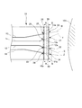
- FIG. 2A is a cross-sectional view in the sensor axial direction (that is, a cross-sectional view parallel to the radial cross-section of the rotating body 103) around the sensor head in the optical sensor according to the present embodiment
- FIG. 2B is a cross-sectional view taken along line AA in FIG.
- FIG. 2C is a view taken along the line BB in FIG. 2A.
- the front end surface 10a of the sensor head 10 faces the peripheral surface of the rotating body 103, and the first illumination optical fiber 11 and the second illumination optical fiber. 12 (first optical fiber), a first light receiving optical fiber 13 (second optical fiber), and a second light receiving optical fiber 14 (third optical fiber).
- the first illumination optical fiber 11 has one end connected to the light emitting device 2 (see FIG. 1) and the other end face (light emitting portion) 11a exposed at the tip face 10a. And it is an optical fiber as a propagation path which radiate
- the second illumination optical fiber 12 has one end connected to the light emitting device 2 and the other end face (light emitting portion) 12a exposed at the tip face 10a. And it is an optical fiber as a propagation path which radiate
- the first illumination optical fiber 11 and the second illumination optical fiber 12 may be connected to different light emitting units.
- One end of the first light receiving optical fiber 13 is connected to the first light receiving device 3 (see FIG. 1), and the end face (light receiving portion) 13a at the other end is exposed at the tip face 10a.
- An optical fiber as a propagation path that receives reflected light, which is illumination light reflected by the peripheral surface of the rotating body 103, at the end surface 13 a and inputs the light to the first light receiving device 3.
- One end of the second light receiving optical fiber 14 is connected to the second light receiving device 4 (see FIG. 1), and the end face (light receiving portion) 14a at the other end is exposed at the tip face 10a.
- Each of the optical fibers 11 to 14 extends substantially in the axial direction of the optical sensor.
- the first light receiving optical fiber 13 and the second light receiving optical fiber 14 extend substantially in the axial direction of the optical sensor, and (at a cross sectional view parallel to the radial cross section of the rotating body 103) Inclined in the shape of a letter C in the direction in which the distance between them increases toward 10a.
- the first illumination optical fiber 11 and the second illumination optical fiber 12 are parallel to the radial cross section of the rotating body 103. (In a cross-sectional view) are arranged to be inclined in a letter C in a direction in which the distance from each other increases toward the tip surface 10a.
- FIG. 2A shows a state in which each of the optical fibers 11, 12, 13, and 14 is arranged one by one.
- the present embodiment is not limited to this, and a plurality of each is provided. Also good.
- the optical sensor according to the present embodiment is measured from the first metal plate 20 (first plate material), which is arranged in close contact with the tip surface 10a in parallel, parallel to the first metal plate 20 and from the first metal plate 20.
- the second metal plate 30 (second plate material) disposed on the front side in the direction (rotating body 103 side), and the environment-resistant window inserted and fixed between the first metal plate 20 and the second metal plate 30 40, which defines the light receiving direction.
- the first metal plate 20 has a first inner through hole 21 formed at a position corresponding to the end surface 11a exposed from the tip surface 10a, and a second inner side formed at a position corresponding to the end surface 12a exposed from the tip surface 10a.
- a through hole 24 is provided.
- the second metal plate 30 is formed at the intersection with the first outer through hole 31 formed at the intersection with the virtual straight line W (identical to the virtual line q) orthogonal to the end surface 11a and the virtual straight line X orthogonal to the end surface 12a.
- the fourth outer through-hole 34 is formed at the intersection.
- first outer through hole 31 and the second outer through hole 32 are larger in diameter than the third outer through hole 33 and the fourth outer through hole 34. This is because the through holes 31 and 32 are through holes for illumination light, and it is preferable that the illumination light is emitted to the rotating body 103 with a certain extent without being reduced.
- the environment-resistant window 40 has a light-transmitting property to transmit illumination light and reflected light, and is made of a material resistant to high heat and high vapor, such as diamond or sapphire (this embodiment is resistant to heat). Although the material of the environmental window 40 is not limited, the environmental window 40 needs to have higher resistance to temperature and steam than at least each optical fiber). Further, the environment-resistant window 40 may be embedded in the through holes 21 to 24 of the first metal plate 20 instead of being inserted between the first metal plate 20 and the second metal plate 30. .
- the optical sensor In the optical sensor according to the present embodiment, first, in the first metal plate 20 and the second metal plate 30, two through holes (the through hole 23 and the through hole 33 or the through hole 24) of these two metal plates are used. Since only the reflected light passing through the through hole 34) is received, the light receiving optical path is defined (similarly, the illumination optical path is also defined). Therefore, even if white turbidity or wear occurs near the end of each optical fiber exposed to harsh environments such as high temperature and high steam environment, the light receiving direction is not affected, and the value of ⁇ in the above equation (1) is not affected. Since there is no fluctuation, the clearance can be measured.
- each optical fiber is not affected even in a high temperature / high steam environment. Therefore, accurate clearance measurement is possible.
- the illumination optical fibers 11 and 12 and the light receiving optical fibers 13 and 14 are spaced apart from each other on the distal end surface 10a. This enables more accurate clearance measurement.
- the environment-resistant window 40 is simply attached between the plate materials (the first metal plate 20 and the second metal plate 30) having the through holes, which is described in Patent Document 1 described above. As compared with metal pore processing, it is advantageous in feasibility and workability.
- the tip surface of the sensor head is parallel to the moving direction with respect to the moving body to be measured. Similar results can be obtained by making them face each other.
- the present invention is suitable as an optical sensor.
Landscapes
- Physics & Mathematics (AREA)
- General Physics & Mathematics (AREA)
- Engineering & Computer Science (AREA)
- Mechanical Engineering (AREA)
- General Engineering & Computer Science (AREA)
- Length Measuring Devices By Optical Means (AREA)
Abstract
センサヘッド(10)の先端面(10a)に端面が露出するようにして配される光ファイバを有する光学センサであって、センサヘッド(10)の先端面(10a)に対し平行に密着し、光ファイバの端面に対応する位置に貫通孔が形成された第1板材(第1金属板)(20)と、第1板材(第1金属板)(20)に対し平行かつ計測方向前方に配され、光ファイバの端面に直交する仮想直線との交点に貫通孔が形成された第2板材(第2金属板)(30)とを備える光学センサを用いることで、光ファイバの白濁化や損耗が生じた場合であってもクリアランス計測を行うことができる。
Description
本発明は、主に回転機械に備わる光学センサに関する。
タービン機械の性能向上のためには、チップクリアランスを小さくする必要がある。そこで、このチップクリアランスを高精度で計測することが求められる。さらには、回転機械全般において、回転側と静止側のクリアランスを高精度で計測することが求められる。
高温・高圧水蒸気環境下でクリアランスを計測するには、解決すべき課題が多く、たとえば、静電容量式のクリアランスセンサは、このような環境下において、劣化による絶縁不良が発生する可能性があり、さらに、誘電率変化の影響を受けるため、使用することができない。
その点、光学センサは、高温・高圧水蒸気環境下において、上述のような影響を受けることがなく、使用に適している。しかし従来の技術では、定性的な変化は捉えることができるが、定量的な計測はできない。
定量的な計測ができない原因として、光学センサに設けられた光ファイバの端部の白濁化や損耗(陥没、減損)が挙げられる。すなわち、高温・高圧水蒸気にさらされた光学センサは、光ファイバの損耗が生じ、また、光ファイバ(端部)は損耗に至る前に表面に白濁化が生じていると考えられている。
光ファイバの端部に白濁化や損耗が生じると、光ファイバに入射する光の方向が変動する。光学センサの計測原理から、光ファイバに入射する光の方向の変動は、クリアランス計測に影響を及ぼす。
よって、高温・高蒸気環境下であっても、光ファイバの白濁化や損耗を生じない光学材料にて光学センサを構成することが理想ではあるが、これは現実的ではない。
したがって本発明では、上記技術的課題に鑑み、光ファイバの白濁化や損耗が生じた場合であってもクリアランス計測可能な光学センサを提供することを目的とする。
上記課題を解決する第1の発明に係る光学センサは、
センサヘッドの先端面に光ファイバの発光部及び受光部が配される光学センサであって、
前記センサヘッドの先端面に対し平行に密着し、前記光ファイバの前記端面に対応する位置に貫通孔が形成された第1板材と、
前記第1板材に対し平行かつ計測対象側に配され、前記光ファイバの発光部及び受光部に直交する仮想直線との交点に貫通孔が形成された第2板材とを備える
ことを特徴とする。
センサヘッドの先端面に光ファイバの発光部及び受光部が配される光学センサであって、
前記センサヘッドの先端面に対し平行に密着し、前記光ファイバの前記端面に対応する位置に貫通孔が形成された第1板材と、
前記第1板材に対し平行かつ計測対象側に配され、前記光ファイバの発光部及び受光部に直交する仮想直線との交点に貫通孔が形成された第2板材とを備える
ことを特徴とする。
上記課題を解決する第2の発明に係る光学センサは、
上記第1の発明に係る光学センサにおいて、
前記センサヘッドの前記先端面が、計測対象である移動体に対し、その移動方向と平行となるように対向しており、
前記光ファイバは、前記移動体からの光を、前記センサヘッドの先端面の受光部にて受光し、第1受光装置に入力する第1受光用光ファイバ及び第2受光装置に入力する第2受光用光ファイバを備え、
前記第1板材の前記貫通孔は、前記第1受光用光ファイバ及び前記第2受光用光ファイバの前記受光部に対応する位置に、それぞれ形成され、
前記第2板材の前記貫通孔は、前記第1受光用光ファイバ及び前記第2受光用光ファイバの前記受光部に直交する仮想直線との交点に、それぞれ形成され、
さらに、前記第1受光装置と前記第2受光装置とにそれぞれ入力される前記移動体からの光のタイミングに基づき、前記移動体とのクリアランスを計測する、測定部を備える
ことを特徴とする。
上記第1の発明に係る光学センサにおいて、
前記センサヘッドの前記先端面が、計測対象である移動体に対し、その移動方向と平行となるように対向しており、
前記光ファイバは、前記移動体からの光を、前記センサヘッドの先端面の受光部にて受光し、第1受光装置に入力する第1受光用光ファイバ及び第2受光装置に入力する第2受光用光ファイバを備え、
前記第1板材の前記貫通孔は、前記第1受光用光ファイバ及び前記第2受光用光ファイバの前記受光部に対応する位置に、それぞれ形成され、
前記第2板材の前記貫通孔は、前記第1受光用光ファイバ及び前記第2受光用光ファイバの前記受光部に直交する仮想直線との交点に、それぞれ形成され、
さらに、前記第1受光装置と前記第2受光装置とにそれぞれ入力される前記移動体からの光のタイミングに基づき、前記移動体とのクリアランスを計測する、測定部を備える
ことを特徴とする。
上記課題を解決する第3の発明に係る光学センサは、
上記第2の発明に係る光学センサにおいて、
前記光ファイバは、発光装置からの照明光を、前記センサヘッドの先端面における発光部から前記移動体に向けて出射する、照明用光ファイバを備え、
前記第1板材の前記貫通孔は、前記第1照明用光ファイバの前記発光部に対応する位置に形成され、
前記第2板材の前記貫通孔は、前記第1照明用光ファイバの前記発光部に直交する仮想直線との交点に形成され、
前記第1受光用光ファイバ及び前記第2受光用光ファイバが受光する前記移動体からの光は、前記照明用光ファイバから出射される前記照明光の反射光である
ことを特徴とする。
上記第2の発明に係る光学センサにおいて、
前記光ファイバは、発光装置からの照明光を、前記センサヘッドの先端面における発光部から前記移動体に向けて出射する、照明用光ファイバを備え、
前記第1板材の前記貫通孔は、前記第1照明用光ファイバの前記発光部に対応する位置に形成され、
前記第2板材の前記貫通孔は、前記第1照明用光ファイバの前記発光部に直交する仮想直線との交点に形成され、
前記第1受光用光ファイバ及び前記第2受光用光ファイバが受光する前記移動体からの光は、前記照明用光ファイバから出射される前記照明光の反射光である
ことを特徴とする。
上記課題を解決する第4の発明に係る光学センサは、
上記第1から3のいずれか1つの発明に係る光学センサにおいて、
前記第1板材と前記第2板材との間に、透光性を有し各前記光ファイバよりも温度及び蒸気への耐性が高い耐環境性窓が挿入される
ことを特徴とする。
上記第1から3のいずれか1つの発明に係る光学センサにおいて、
前記第1板材と前記第2板材との間に、透光性を有し各前記光ファイバよりも温度及び蒸気への耐性が高い耐環境性窓が挿入される
ことを特徴とする。
上記課題を解決する第5の発明に係る光学センサは、
上記第1から3のいずれか1つの発明に係る光学センサにおいて、
前記第1板材の前記貫通孔に、透光性を有し各前記光ファイバよりも温度及び蒸気への耐性が高い耐環境性窓が埋め込まれる
ことを特徴とする。
上記第1から3のいずれか1つの発明に係る光学センサにおいて、
前記第1板材の前記貫通孔に、透光性を有し各前記光ファイバよりも温度及び蒸気への耐性が高い耐環境性窓が埋め込まれる
ことを特徴とする。
上記課題を解決する第6の発明に係る光学センサは、
上記第3から5のいずれか1つの発明に係る光学センサにおいて、
前記照明用光ファイバの端面は、前記センサヘッドの先端面において、前記第1受光用光ファイバ及び前記第2受光用光ファイバの前記受光部から離隔して配される
ことを特徴とする。
上記第3から5のいずれか1つの発明に係る光学センサにおいて、
前記照明用光ファイバの端面は、前記センサヘッドの先端面において、前記第1受光用光ファイバ及び前記第2受光用光ファイバの前記受光部から離隔して配される
ことを特徴とする。
上記課題を解決する第7の発明に係る光学センサは、
上記第3から6のいずれか1つの発明に係る光学センサにおいて、
前記第2板材において、前記照明用光ファイバの前記発光部に直交する仮想直線との交点に形成される前記貫通孔は、前記第1受光用光ファイバ及び前記第2受光用光ファイバの前記受光部に直交する仮想直線との交点にそれぞれ形成される各前記貫通孔よりも、径が大きい
ことを特徴とする。
上記第3から6のいずれか1つの発明に係る光学センサにおいて、
前記第2板材において、前記照明用光ファイバの前記発光部に直交する仮想直線との交点に形成される前記貫通孔は、前記第1受光用光ファイバ及び前記第2受光用光ファイバの前記受光部に直交する仮想直線との交点にそれぞれ形成される各前記貫通孔よりも、径が大きい
ことを特徴とする。
本発明に係る光学センサによれば、光ファイバの白濁化や損耗が生じた場合であってもクリアランス計測を行うことができる。
図1は、回転機械に配置された本発明に係る光学センサを説明する概略図である。図1に示すように、該回転機械は、ハウジング101内において、回転軸102に固定され、ハウジング101の内周面とクリアランスを有して配された回転体103を備えている。そして、本発明に係る光学センサは、先端が、ハウジング101の内周面に、回転体103の周面と対向して配されるようにして、該回転機械に設けられている。
より詳述すると、本発明に係る光学センサは、ハウジング101の内周面において、先端面が計測対象である回転体103側を向くようにして配されるセンサ部1、第1の光ファイバを介してセンサ部1に接続する発光装置(光源)2、第2の光ファイバを介してセンサ部1に接続する第1受光装置3、第3の光ファイバを介してセンサ部1に接続する第2受光装置4、及び、第1受光装置3及び第2受光装置4に接続する測定部5を備えている(図1中では、第1~3の光ファイバをまとめて符号6で示している)。
計測の手順としては、まず、回転機械の駆動中において、発光装置2から第1の光ファイバを介してセンサ部1へ照明光が出力され、この照明光がセンサ部1の先端部(センサヘッド)から回転体103へ向けて出射(放出)される。
照明光は回転体103の周面において反射し、その反射光の一部は、センサヘッドに入射し、第2の光ファイバを介して第1受光装置3へ、第3の光ファイバを介して第2受光装置4へそれぞれ入力される。
このとき、回転体103からセンサヘッドに入射する反射光は、回転体103の周面において周方向(回転方向)に変化する形状あるいは模様に依存した、所定の強度周期を有している。この「形状」は、例えば、回転体103がタービンである場合には動翼の形状となる。また「模様」とは、回転体103の周面において周方向に変化する形状がない場合、例えば、マーカ等を付すことによって明暗を設けているものを指す。
測定部5では、第1受光装置3及び第2受光装置4にそれぞれ入力される(回転体103の周面からの)反射光のタイミングに基づき、回転体103とのクリアランスを計測する。
以上が、本発明に係る光学センサによる回転機械のクリアランス計測の手順である。
以上が、本発明に係る光学センサによる回転機械のクリアランス計測の手順である。
以下、本発明に係る光学センサを実施例にて詳述する。なお、下記実施例では、一部タービンに光学センサを配するものとして説明している箇所があるが、本発明はこれに限らず、回転機械全般に適用可能である。
さらに言えば、本発明に係る光学センサは、下記実施例中に説明する原理(下記(1)式及び図4)上、回転機械の回転体に限らず、移動体であればクリアランスを計測することができる。
[実施例1]
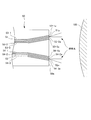
図3Aは、従来の光学センサの初期(通常)状態におけるセンサヘッド周辺の、センサ軸方向断面図(回転体103の径方向断面と平行な断面図)であり、図3Bは、従来の光学センサの白濁化あるいは損耗後の状態におけるセンサヘッド周辺の、センサ軸方向断面図である。まず、図3Aにて初期状態について説明する。
図3Aは、従来の光学センサの初期(通常)状態におけるセンサヘッド周辺の、センサ軸方向断面図(回転体103の径方向断面と平行な断面図)であり、図3Bは、従来の光学センサの白濁化あるいは損耗後の状態におけるセンサヘッド周辺の、センサ軸方向断面図である。まず、図3Aにて初期状態について説明する。
従来の光学センサは、センサヘッド50の先端面50aが回転体103の周面に対向し、照明用光ファイバ51,52(第1の光ファイバ)、第1受光用光ファイバ53‐1,53‐2,53‐3(第2の光ファイバ)、及び、第2受光用光ファイバ54‐1,54‐2,54‐3(第3の光ファイバ)を備えている。
照明用光ファイバ51,52は、それぞれ、一端が発光装置2(図1参照)に接続し、他端の端面(発光部)51a,52aが先端面50aにおいて露出している。そして、発光装置2から出力された照明光を、端面51a,52aから、回転体103の周面に向けて出射する伝搬経路としての光ファイバである。
第1受光用光ファイバ53‐1,53‐2,53‐3は、それぞれ、一端が第1受光装置3(図1参照)に接続し、他端の端面(受光部)53‐1a,53‐2a,53‐3aが先端面50aにおいて露出している。そして、回転体103の周面にて反射された照明光である反射光を、端面53‐1a,53‐2a,53‐3aにて受光(入射)し、第1受光装置3へ入力する伝搬経路としての光ファイバである。
第2受光用光ファイバ54‐1,54‐2,54‐3は、一端が第2受光装置4(図1参照)に接続し、他端の端面(受光部)54‐1a,54‐2a,54‐3aが先端面50aにおいて露出している。そして、回転体103の周面にて反射された照明光である反射光を、端面54‐1a,54‐2a,54‐3aにて受光し、第2受光装置4へ入力する伝搬経路としての光ファイバである。
またここでは、第1受光用光ファイバ53‐1,53‐2,53‐3、及び、照明用光ファイバ51が、一組に纏められており、これを光ファイバ群Pとする。さらに、第2受光用光ファイバ54‐1,54‐2,54‐3、及び、照明用光ファイバ52が、一組に纏められており、これを光ファイバ群Qとする。
光ファイバ群P,Qは、光学センサの略軸方向に延伸し、センサヘッド50内部では、(回転体103の径方向断面と平行な断面視において)先端面50aに向けて互いの離間距離が広がる方向にハの字に傾斜している。また、光ファイバ群P,Qは、先端面50aにおいて、端面53‐1a,53‐2a,53‐3a及び端面51aの位置及び角度と、端面54‐1a,54‐2a,54‐3a及び端面52aの位置及び角度とが、光学センサのセンサ軸方向中心線を中心として対称的に配されている。
以上が従来の光学センサの構成である。なお、従来の光学センサを用いたクリアランスの計測手順は、図1を用いて説明した如くである。
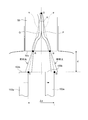
図4は、タービンを例として、光学センサによるクリアランス(チップクリアランス)計測を説明する模式図であり、図中の破線矢印は、回転体103(図1参照)の動翼103aの回転方向を示している。
先端面50aにおける光ファイバ群Qの端面54‐1a,54‐2a,54‐3a及び端面52aの位置をA点(詳細には端面の位置は4箇所となるが、光ファイバ54‐1,54‐2,54‐3,52は一纏まりのため隣接しており、端面の位置(及び角度)が略同一であるため、一つの点と見做す)とし、光ファイバ群Pの端面53‐1a,53‐2a,53‐3a及び端面51aの位置をB点(A点同様に一つの点と見做す)。
さらに、A点とB点との離間距離をLとし、端面53‐1a,53‐2a,53‐3aに直交する仮想直線p(上述と同様に、詳細には3本の仮想直線を1本と見做す)、端面54‐1a,54‐2a,54‐3aに直交する仮想直線q(上述と同様に、詳細には3本の仮想直線を1本と見做す)、及び、センサ軸方向中心線の3つの線の交点が、距離計測の基準点Oとなり、距離計測の基準点Oにおける仮想直線p,qの交差角をαとする。
また、動翼103aの外側端面103bにおける角部(二つの角部のうち回転方向前方側の角部)が、仮想直線qと交わる点をC点とし、仮想直線pと交わる点をD点とする。なお、この角部とは、第1受光用光ファイバ33及び第2受光用光ファイバ34へ入射する反射光の強度が(急激に)変化する箇所である。
さらに、動翼103aが、C点からD点まで移動する時間をΔtとし、光学センサの先端面31aと動翼103aの外側端面103bとのクリアランス(計測すべきクリアランス)をdとする。
すると、下記(1)式が成立する。

ただし、Rを回転体半径、Tを回転体の周期とする。
なお、上記(1)式は、光ファイバ群p,qにそれぞれ受光用光ファイバが1本ずつ含まれていれば成立する。また、上記(1)式中に照明用光ファイバに関わる係数は出てこないため、照明光が回転体103で反射した反射光を受光用光ファイバで受光できさえすれば、照明用光ファイバの端面は、A,B点からそれぞれ外れた位置にあってもよい(その場合、A,B点は、受光用光ファイバの端面のみの位置を示すことになる)。
従来の光学センサでは、図3Aに示すように、先端面50aに端面53‐1a,53‐2a,53‐3a,54‐1a,54‐2a,54‐3a、及び、端面51a,52aがあることで、先端面50aにおいて照明光が出射され反射光を受光している場合は、上記(1)式が成立する。
しかしながら、図3Bに示すように、各光ファイバ51,52,53‐1,53‐2,53‐3,54‐1,54‐2,54‐3に、白濁化あるいは損耗が発生すると、照明光の出射位置及び光の広がりがランダム化し、それとともに、反射光の受光位置及び受光角度もランダム化してしまい、上記(1)式におけるαが不確定となり、上記(1)式は成立しなくなる。
また、上記特許文献1に記載されるように、光ファイバの先端部分に嵌合する金属細孔を有するパイプを設け、この金属細孔により光路を確実に規定することもできるが、このような方法では、金属細孔の径が小さいため正確に形成することが難しい。
一方、本実施例に係る光学センサでは、貫通孔の形成された2つの金属板及び耐環境性窓を設けることで、各光ファイバに白濁化や損耗が発生した場合にも、上記(1)式を成立させ、クリアランス計測ができ、さらに、上記特許文献1に記載された光学センサに比べ、簡易的に作製することを可能とするものである。
図2Aは、本実施例に係る光学センサにおけるセンサヘッド周辺の、センサ軸方向断面図(すなわち回転体103の径方向断面と平行な断面図)であり、図2Bは、図2AのA‐A矢視図であり、図2Cは、図2AのB‐B矢視図である。
本実施例に係る光学センサは、まず、図2Aに示すように、センサヘッド10の先端面10aが回転体103の周面に対向し、第1照明用光ファイバ11と第2照明用光ファイバ12(第1の光ファイバ)、第1受光用光ファイバ13(第2の光ファイバ)、及び、第2受光用光ファイバ14(第3の光ファイバ)を備えている。
第1照明用光ファイバ11は、一端が発光装置2(図1参照)に接続し、他端の端面(発光部)11aが先端面10aにおいて露出している。そして、発光装置2から出力された照明光を、端面11aから、回転体103の周面に向けて出射する伝搬経路としての光ファイバである。
第2照明用光ファイバ12は、一端が発光装置2に接続し、他端の端面(発光部)12aが先端面10aにおいて露出している。そして、発光装置2から出力された照明光を、端面12aから、回転体103の周面に向けて出射する伝搬経路としての光ファイバである。なお、第1照明用光ファイバ11と第2照明用光ファイバ12とは、別々の発光部に接続しているものとしてもよい。
第1受光用光ファイバ13は、一端が第1受光装置3(図1参照)に接続し、他端の端面(受光部)13aが先端面10aにおいて露出している。そして、回転体103の周面にて反射された照明光である反射光を、端面13aにて受光し、第1受光装置3へ入力する伝搬経路としての光ファイバである。
第2受光用光ファイバ14は、一端が第2受光装置4(図1参照)に接続し、他端の端面(受光部)14aが先端面10aにおいて露出している。そして、回転体103の周面にて反射された照明光である反射光を、端面14aにて受光し、第2受光装置4へ入力する伝搬経路としての光ファイバである。
各光ファイバ11~14は、光学センサの略軸方向に延伸している。センサヘッド10内部では、第1受光用光ファイバ13及び第2受光用光ファイバ14は、光学センサの略軸方向に延伸し、(回転体103の径方向断面と平行な断面視において)先端面10aに向けて互いの離間距離が広がる方向にハの字に傾斜して配される。さらに、第1受光用光ファイバ13と第2受光用光ファイバ14との間において、第1照明用光ファイバ11及び第2照明用光ファイバ12は、(回転体103の径方向断面と平行な断面視において)先端面10aに向けて互いの離間距離が広がる方向にハの字に傾斜して配される。
また、先端面10aでは、(回転体103の径方向断面と平行な断面視において)端面11a~14aが互いに隔離して配されている。なお、図2Aには、各光ファイバ11,12,13,14がそれぞれ1本ずつ配されている状態を示しているが、本実施例はこれに限定されず、それぞれを複数本ずつにしてもよい。
さらに、本実施例に係る光学センサは、先端面10aに対し平行に密着して配された第1金属板20(第1板材)、第1金属板20と平行かつ第1金属板20より計測方向前方側(回転体103側)に配された第2金属板30(第2板材)、及び、第1金属板20と第2金属板30との間に挿入され固定された耐環境性窓40を備え、これにより受光方向を規定している。
第1金属板20は、先端面10aから露出した端面11aに対応する位置に形成される第1内側貫通孔21、同じく先端面10aから露出した端面12aに対応する位置に形成される第2内側貫通孔22、同じく先端面10aから露出した端面13aに対応する位置に形成される第3内側貫通孔23、及び、同じく先端面10aから露出した端面14aに対応する位置に形成される第4内側貫通孔24を備えている。
第2金属板30は、端面11aに直交する仮想直線W(上記仮想直線qと同一)との交点に形成される第1外側貫通孔31、端面12aに直交する仮想直線Xとの交点に形成される第2外側貫通孔32、端面13aに直交する仮想直線Yとの交点に形成される第3外側貫通孔33、及び、端面14aに直交する仮想直線Z(上記仮想直線pと同一)との交点に形成される第4外側貫通孔34を備えている。
また、第1外側貫通孔31及び第2外側貫通孔32は、第3外側貫通孔33及び第4外側貫通孔34に比べ径が大きくなっている。貫通孔31,32は照明光用の貫通孔であり、照明光については、あまり絞らずにある程度の広がりをもって回転体103に出射した方が好ましいためである。
耐環境性窓40は、照明光及び反射光を透過させる透光性を有し、高熱及び高蒸気に耐性のある材質、例えばダイヤモンドあるいはサファイアなどにより構成されるものとする(本実施例は耐環境性窓40の材質を限定するものではないが、耐環境性窓40は少なくとも各光ファイバよりも温度及び蒸気への耐性が高い必要がある)。また、耐環境性窓40は、第1金属板20と第2金属板30との間に挿入されるのではなく、第1金属板20の貫通孔21~24にそれぞれ埋め込まれるものとしてもよい。
以上が本実施例に係る光学センサの構成である。なお、本実施例に係る光学センサを用いたクリアランスの計測手順は、図1を用いて説明した如くである。
本実施例に係る光学センサは、まず、第1金属板20及び第2金属板30にて、これら2つの金属板の2つの貫通孔(貫通孔23と貫通孔33、又は、貫通孔24と貫通孔34)を通過する反射光のみしか受光しないことになるため、受光光路が規定される(同様に照明光路も規定される)。そのため、高温・高蒸気環境等の過酷環境下にさらされる各光ファイバの端部付近に白濁化や損耗が発生した場合でも、受光方向に影響がなく、上記(1)式におけるαの値に変動がないため、クリアランス計測が可能となる。
また、耐環境性窓40により、先端面10aを封止することで、高温・高蒸気環境下でも各光ファイバがその影響を受けることがない。よって、正確なクリアランス計測が可能となる。
さらに、本実施例に係る光学センサでは、照明用光ファイバ11,12と受光用光ファイバ13,14とが、先端面10aにおいて離隔して配されるため、送受光の干渉を低減することができ、より正確なクリアランス計測が可能となる。
また、本実施例に係る光学センサでは、貫通孔を開けた板材(第1金属版20及び第2金属板30)の間に耐環境性窓40を取り付けるだけであり、上記特許文献1に記載されるような、金属細孔加工と比較し、実現性及び加工性において有利である。
また、本発明に係る光学センサを、回転体以外も含めた移動体に対するクリアランスの計測に用いる場合には、センサヘッドの先端面を、計測対象である移動体に対し、その移動方向と平行となるように対向させれば、同様の結果を得ることができる。
本発明は、光学センサとして好適である。
1 センサ部
2 発光装置
3 第1受光装置
4 第2受光装置
5 測定部
6 各光ファイバ
10,50 センサヘッド
10a,50a (センサヘッドの)先端面
11 第1照明用光ファイバ
11a (第1照明用光ファイバの)端面(発光部)
12 第2照明用光ファイバ
12a (第2照明用光ファイバの)端面(発光部)
13,53‐1,53‐2,53‐3 第1受光用光ファイバ
13a,53‐1a,53‐2a,53‐3a (第1受光用光ファイバの)端面(受光部)
14,54‐1,54‐2,54‐3 第2受光用光ファイバ
14a,54‐1a,54‐2a,54‐3a (第2受光用光ファイバの)端面(受光部)
20 第1金属板(第1板材)
21 第1内側貫通孔
22 第2内側貫通孔
23 第3内側貫通孔
24 第4内側貫通孔
30 第2金属板(第2板材)
31 第1外側貫通孔
32 第2外側貫通孔
33 第3外側貫通孔
34 第4外側貫通孔
40 耐環境性窓
51,52 照明用光ファイバ
51a,52a (照明用光ファイバの)端面(発光部)
101 ハウジング
102 回転軸
103 回転体
103a 動翼
103b 外側端面
2 発光装置
3 第1受光装置
4 第2受光装置
5 測定部
6 各光ファイバ
10,50 センサヘッド
10a,50a (センサヘッドの)先端面
11 第1照明用光ファイバ
11a (第1照明用光ファイバの)端面(発光部)
12 第2照明用光ファイバ
12a (第2照明用光ファイバの)端面(発光部)
13,53‐1,53‐2,53‐3 第1受光用光ファイバ
13a,53‐1a,53‐2a,53‐3a (第1受光用光ファイバの)端面(受光部)
14,54‐1,54‐2,54‐3 第2受光用光ファイバ
14a,54‐1a,54‐2a,54‐3a (第2受光用光ファイバの)端面(受光部)
20 第1金属板(第1板材)
21 第1内側貫通孔
22 第2内側貫通孔
23 第3内側貫通孔
24 第4内側貫通孔
30 第2金属板(第2板材)
31 第1外側貫通孔
32 第2外側貫通孔
33 第3外側貫通孔
34 第4外側貫通孔
40 耐環境性窓
51,52 照明用光ファイバ
51a,52a (照明用光ファイバの)端面(発光部)
101 ハウジング
102 回転軸
103 回転体
103a 動翼
103b 外側端面
Claims (7)
- センサヘッドの先端面に光ファイバの発光部及び受光部が配される光学センサであって、
前記センサヘッドの先端面に対し平行に密着し、前記光ファイバの前記端面に対応する位置に貫通孔が形成された第1板材と、
前記第1板材に対し平行かつ計測対象側に配され、前記光ファイバの発光部及び受光部に直交する仮想直線との交点に貫通孔が形成された第2板材とを備える
ことを特徴とする光学センサ。 - 前記センサヘッドの前記先端面が、計測対象である移動体に対向して配置されており、
前記光ファイバは、前記移動体からの光を、前記センサヘッドの先端面の受光部にて受光し、第1受光装置に入力する第1受光用光ファイバ及び第2受光装置に入力する第2受光用光ファイバを備え、
前記第1板材の前記貫通孔は、前記第1受光用光ファイバ及び前記第2受光用光ファイバの前記受光部に対応する位置に、それぞれ形成され、
前記第2板材の前記貫通孔は、前記第1受光用光ファイバ及び前記第2受光用光ファイバの前記受光部に直交する仮想直線との交点に、それぞれ形成され、
さらに、前記第1受光装置と前記第2受光装置とにそれぞれ入力される前記移動体からの光のタイミングに基づき、前記移動体とのクリアランスを計測する、測定部を備える
ことを特徴とする請求項1に記載の光学センサ。 - 前記光ファイバは、発光装置からの照明光を、前記センサヘッドの先端面における発光部から前記移動体に向けて出射する、照明用光ファイバを備え、
前記第1板材の前記貫通孔は、前記第1照明用光ファイバの前記発光部に対応する位置に形成され、
前記第2板材の前記貫通孔は、前記第1照明用光ファイバの前記発光部に直交する仮想直線との交点に形成され、
前記第1受光用光ファイバ及び前記第2受光用光ファイバが受光する前記移動体からの光は、前記照明用光ファイバから出射される前記照明光の反射光である
ことを特徴とする請求項2に記載の光学センサ。 - 前記第1板材と前記第2板材との間に、透光性を有し各前記光ファイバよりも温度及び蒸気への耐性が高い耐環境性窓が挿入される
ことを特徴とする請求項1から3のいずれか1項に記載の光学センサ。 - 前記第1板材の各前記貫通孔に、透光性を有し各前記光ファイバよりも温度及び蒸気への耐性が高い耐環境性窓がそれぞれ埋め込まれる
ことを特徴とする請求項1から3のいずれか1項に記載の光学センサ。 - 前記照明用光ファイバの端面は、前記センサヘッドの先端面において、前記第1受光用光ファイバ及び前記第2受光用光ファイバの前記受光部から離隔して配される
ことを特徴とする請求項3から5のいずれか1項に記載の光学センサ。 - 前記第2板材において、前記照明用光ファイバの前記発光部に直交する仮想直線との交点に形成される前記貫通孔は、前記第1受光用光ファイバ及び前記第2受光用光ファイバの前記受光部に直交する仮想直線との交点にそれぞれ形成される各前記貫通孔よりも、径が大きい
ことを特徴とする請求項3から6のいずれか1項に記載の光学センサ。
Priority Applications (2)
| Application Number | Priority Date | Filing Date | Title |
|---|---|---|---|
| CN201780034865.1A CN109313013B (zh) | 2016-06-07 | 2017-06-07 | 光学传感器 |
| US16/308,054 US10760897B2 (en) | 2016-06-07 | 2017-06-07 | Optical sensor |
Applications Claiming Priority (2)
| Application Number | Priority Date | Filing Date | Title |
|---|---|---|---|
| JP2016-113203 | 2016-06-07 | ||
| JP2016113203A JP6599285B2 (ja) | 2016-06-07 | 2016-06-07 | 光学センサ |
Publications (1)
| Publication Number | Publication Date |
|---|---|
| WO2017213161A1 true WO2017213161A1 (ja) | 2017-12-14 |
Family
ID=60578614
Family Applications (1)
| Application Number | Title | Priority Date | Filing Date |
|---|---|---|---|
| PCT/JP2017/021053 Ceased WO2017213161A1 (ja) | 2016-06-07 | 2017-06-07 | 光学センサ |
Country Status (4)
| Country | Link |
|---|---|
| US (1) | US10760897B2 (ja) |
| JP (1) | JP6599285B2 (ja) |
| CN (1) | CN109313013B (ja) |
| WO (1) | WO2017213161A1 (ja) |
Families Citing this family (1)
| Publication number | Priority date | Publication date | Assignee | Title |
|---|---|---|---|---|
| US12339113B2 (en) * | 2022-06-30 | 2025-06-24 | Ge Infrastructure Technology Llc | Apparatus and method for transmitting radiation to a rotating component |
Citations (7)
| Publication number | Priority date | Publication date | Assignee | Title |
|---|---|---|---|---|
| JPH0518981A (ja) * | 1991-07-10 | 1993-01-26 | Nippon Kagaku Kogyo Kk | 気液二相流の計測装置 |
| US5274721A (en) * | 1992-03-05 | 1993-12-28 | American Sigma, Inc. | Fiber optic system and method |
| JPH0763509A (ja) * | 1993-06-30 | 1995-03-10 | Mitsubishi Rayon Co Ltd | 光ファイバセンサヘッド |
| JP2004191374A (ja) * | 2002-12-12 | 2004-07-08 | Siemens Ag | 距離測定方法および距離測定装置 |
| JP2004333470A (ja) * | 2003-05-07 | 2004-11-25 | Mitsutoyo Corp | 光ファイバ受信器チャネルを使用した2次元測定装置 |
| JP2005326362A (ja) * | 2004-05-17 | 2005-11-24 | Keyence Corp | 光電センサ |
| JP2015001414A (ja) * | 2013-06-14 | 2015-01-05 | 三菱重工業株式会社 | チップクリアランス計測装置 |
Family Cites Families (15)
| Publication number | Priority date | Publication date | Assignee | Title |
|---|---|---|---|---|
| US4275965A (en) * | 1979-08-21 | 1981-06-30 | United Technologies Corporation | Long stroke, high resolution optical position sensor |
| JPS59134026A (ja) | 1983-01-24 | 1984-08-01 | Nissan Motor Co Ltd | 自動車用キヤリア |
| US5299141A (en) | 1989-12-22 | 1994-03-29 | American Sigma, Inc. | Automatic fluid monitoring and sampling apparatus and method |
| JPH10132752A (ja) * | 1996-09-04 | 1998-05-22 | Asahi Kooden Kk | ライトガイド |
| CN1161505C (zh) | 1997-11-06 | 2004-08-11 | 伊斯曼化学公司 | 共聚酯粘合用纤维 |
| JP3854056B2 (ja) * | 1999-12-13 | 2006-12-06 | 株式会社荏原製作所 | 基板膜厚測定方法、基板膜厚測定装置、基板処理方法及び基板処理装置 |
| KR20030068582A (ko) * | 2001-01-09 | 2003-08-21 | 무코우다, 타카히코 | 다코어 광섬유용 커넥터, 페룰, 및 그 제조방법 |
| US20040125702A1 (en) * | 2002-10-21 | 2004-07-01 | Hideki Kitajima | Rotational position detection device, hand position detection device and clock using the hand position detection device |
| JP2004246279A (ja) * | 2003-02-17 | 2004-09-02 | Seiko Epson Corp | 光モジュール及びその製造方法、光通信装置、光電気混載集積回路、回路基板、電子機器 |
| US20080291456A1 (en) * | 2007-05-24 | 2008-11-27 | Ghislain Lucien P | Sensor apparatus and method using optical interferometry |
| KR200444690Y1 (ko) * | 2009-02-03 | 2009-05-28 | (주)위니테크놀러지 | 광케이블 여장처리구조가 구비된 다심형 화이버 광스위치 모듈 |
| CN201477265U (zh) * | 2009-08-19 | 2010-05-19 | 浙江万马集团电子有限公司 | 光分路器模块夹具插片 |
| CN201965258U (zh) * | 2010-12-10 | 2011-09-07 | 富士康(昆山)电脑接插件有限公司 | 光纤连接器 |
| CN202166608U (zh) * | 2011-06-30 | 2012-03-14 | 深圳市汇松科技发展有限公司 | 一种多通道酶标仪的检测体组 |
| CN104501728A (zh) * | 2014-12-12 | 2015-04-08 | 天津大学 | 一种基于全光纤叶尖定时的叶尖间隙测量方法 |
-
2016
- 2016-06-07 JP JP2016113203A patent/JP6599285B2/ja active Active
-
2017
- 2017-06-07 WO PCT/JP2017/021053 patent/WO2017213161A1/ja not_active Ceased
- 2017-06-07 CN CN201780034865.1A patent/CN109313013B/zh active Active
- 2017-06-07 US US16/308,054 patent/US10760897B2/en active Active
Patent Citations (7)
| Publication number | Priority date | Publication date | Assignee | Title |
|---|---|---|---|---|
| JPH0518981A (ja) * | 1991-07-10 | 1993-01-26 | Nippon Kagaku Kogyo Kk | 気液二相流の計測装置 |
| US5274721A (en) * | 1992-03-05 | 1993-12-28 | American Sigma, Inc. | Fiber optic system and method |
| JPH0763509A (ja) * | 1993-06-30 | 1995-03-10 | Mitsubishi Rayon Co Ltd | 光ファイバセンサヘッド |
| JP2004191374A (ja) * | 2002-12-12 | 2004-07-08 | Siemens Ag | 距離測定方法および距離測定装置 |
| JP2004333470A (ja) * | 2003-05-07 | 2004-11-25 | Mitsutoyo Corp | 光ファイバ受信器チャネルを使用した2次元測定装置 |
| JP2005326362A (ja) * | 2004-05-17 | 2005-11-24 | Keyence Corp | 光電センサ |
| JP2015001414A (ja) * | 2013-06-14 | 2015-01-05 | 三菱重工業株式会社 | チップクリアランス計測装置 |
Also Published As
| Publication number | Publication date |
|---|---|
| US10760897B2 (en) | 2020-09-01 |
| JP2017219391A (ja) | 2017-12-14 |
| US20190310075A1 (en) | 2019-10-10 |
| JP6599285B2 (ja) | 2019-10-30 |
| CN109313013B (zh) | 2021-06-01 |
| CN109313013A (zh) | 2019-02-05 |
Similar Documents
| Publication | Publication Date | Title |
|---|---|---|
| CN203100688U (zh) | 一种测量旋转叶片叶尖间隙的光纤传感器 | |
| FI125320B (en) | ORGANIZATION AND SIMILAR METHOD FOR OPTICAL MEASUREMENTS | |
| ATE414273T1 (de) | Vorrichtung zur inspektion einer oberfläche | |
| FI125408B (fi) | Menetelmä ja mittalaite pinnan etäisyyden, kohteen paksuuden ja optisten ominaisuuksien mittaamiseksi | |
| CN104215197B (zh) | 基于低反射率三芯光纤光栅阵列空间形状测量装置及方法 | |
| KR101954300B1 (ko) | 투과 및/또는 반사 특성을 판단하기 위한 측정방법 및 측정기기 | |
| RU2009124266A (ru) | Волоконно-оптическая система и способ измерения множественных параметров турбомашинной системы | |
| CN109416244B (zh) | 间隙计测装置和间隙控制系统 | |
| US9791594B2 (en) | Light grid with detection by adjacent light reception units arranged opposite light transmission units | |
| KR101856595B1 (ko) | 국소 굴절률의 측정 방법 및 장치 | |
| JP6599285B2 (ja) | 光学センサ | |
| CN102607696B (zh) | 一种用于led测试机的积分球 | |
| CN102607412A (zh) | 视觉测量系统中相机转动轴位置测量方法 | |
| JP2013205332A (ja) | 欠点検査装置および欠点検査方法 | |
| CN101571479A (zh) | 基于线阵ccd的光学液体浓度测量装置及测量方法 | |
| JP6959027B2 (ja) | クリアランス計測装置、クリアランス計測センサ及びクリアランス計測方法 | |
| CN204422058U (zh) | 一种基于激光的桥梁振动检测装置 | |
| CN108885091B (zh) | 光学传感器及旋转机械 | |
| ATE487116T1 (de) | System und verfahren zum messen von distanzen, verschiebungen und mechanischen einwirkungen | |
| CN208282795U (zh) | 基于双曲面透镜的角度传感器 | |
| KR101551259B1 (ko) | 광세기 기반 광섬유 센서 헤드 | |
| JP2017181238A5 (ja) | 光学センサ及び回転機械 | |
| JP2017219391A5 (ja) | ||
| JP2014228364A (ja) | ボア変形量測定装置 | |
| WO2017164149A1 (ja) | 光学センサ、回転機械及びクリアランス計測方法 |
Legal Events
| Date | Code | Title | Description |
|---|---|---|---|
| 121 | Ep: the epo has been informed by wipo that ep was designated in this application |
Ref document number: 17810335 Country of ref document: EP Kind code of ref document: A1 |
|
| NENP | Non-entry into the national phase |
Ref country code: DE |
|
| 122 | Ep: pct application non-entry in european phase |
Ref document number: 17810335 Country of ref document: EP Kind code of ref document: A1 |