WO2017212865A1 - インクジェットヘッドの駆動波形信号出力装置、インクジェット記録装置及びインクジェットヘッドの駆動波形信号出力方法 - Google Patents
インクジェットヘッドの駆動波形信号出力装置、インクジェット記録装置及びインクジェットヘッドの駆動波形信号出力方法 Download PDFInfo
- Publication number
- WO2017212865A1 WO2017212865A1 PCT/JP2017/017974 JP2017017974W WO2017212865A1 WO 2017212865 A1 WO2017212865 A1 WO 2017212865A1 JP 2017017974 W JP2017017974 W JP 2017017974W WO 2017212865 A1 WO2017212865 A1 WO 2017212865A1
- Authority
- WO
- WIPO (PCT)
- Prior art keywords
- waveform
- drive
- signal
- drive waveform
- voltage
- Prior art date
- Legal status (The legal status is an assumption and is not a legal conclusion. Google has not performed a legal analysis and makes no representation as to the accuracy of the status listed.)
- Ceased
Links
Images




Classifications
-
- B—PERFORMING OPERATIONS; TRANSPORTING
- B41—PRINTING; LINING MACHINES; TYPEWRITERS; STAMPS
- B41J—TYPEWRITERS; SELECTIVE PRINTING MECHANISMS, i.e. MECHANISMS PRINTING OTHERWISE THAN FROM A FORME; CORRECTION OF TYPOGRAPHICAL ERRORS
- B41J2/00—Typewriters or selective printing mechanisms characterised by the printing or marking process for which they are designed
- B41J2/005—Typewriters or selective printing mechanisms characterised by the printing or marking process for which they are designed characterised by bringing liquid or particles selectively into contact with a printing material
- B41J2/01—Ink jet
- B41J2/015—Ink jet characterised by the jet generation process
-
- B—PERFORMING OPERATIONS; TRANSPORTING
- B41—PRINTING; LINING MACHINES; TYPEWRITERS; STAMPS
- B41J—TYPEWRITERS; SELECTIVE PRINTING MECHANISMS, i.e. MECHANISMS PRINTING OTHERWISE THAN FROM A FORME; CORRECTION OF TYPOGRAPHICAL ERRORS
- B41J2/00—Typewriters or selective printing mechanisms characterised by the printing or marking process for which they are designed
- B41J2/005—Typewriters or selective printing mechanisms characterised by the printing or marking process for which they are designed characterised by bringing liquid or particles selectively into contact with a printing material
- B41J2/01—Ink jet
- B41J2/015—Ink jet characterised by the jet generation process
- B41J2/04—Ink jet characterised by the jet generation process generating single droplets or particles on demand
- B41J2/045—Ink jet characterised by the jet generation process generating single droplets or particles on demand by pressure, e.g. electromechanical transducers
Definitions
- the present invention relates to an inkjet head drive waveform signal output apparatus, an inkjet recording apparatus, and an inkjet head drive waveform signal output method.
- an ink jet recording apparatus that records an image by ejecting ink from a nozzle.
- a pressure change is generated in ink in a pressure chamber communicating with the nozzle, whereby ink is ejected from the nozzle as droplets having an appropriate shape and liquid amount.
- One of the elements used to cause a pressure change in a pressure chamber in an ink jet recording apparatus is a piezoelectric element, and an appropriate voltage is applied to the piezoelectric element to control a deformation amount and a deformation time.
- the piezoelectric element is a capacitive load, and switches whether or not ink is ejected from a large number of arranged nozzles, and applies a voltage to the piezoelectric element corresponding to each nozzle that ejects ink according to the switching. Then, the total amount of electric charge that flows from the drive circuit to the piezoelectric element and flows out of the piezoelectric element changes according to the number of piezoelectric elements to which a voltage is applied. Therefore, in order to supply the drive waveform stably, there is a problem that sufficient power supply is required and power consumption increases.
- Patent Document 1 discloses that an output signal obtained by filtering a drive waveform signal obtained by class D amplification by an LC circuit is fed back by advancing the phase, and a differential signal is fed back independently, thereby filtering the LC circuit while suppressing power loss. A technique for maintaining a stable frequency and outputting an appropriate waveform is disclosed.
- the magnitude of the current supplied to the piezoelectric element changes by several orders of magnitude. If a power supply unit capable of supplying sufficient power in accordance with such maximum current is prepared, there is a problem that the power supply unit becomes larger than necessary. On the other hand, when a drive waveform is applied at a high speed without increasing the size of the power supply unit, there is a problem that the drive waveform signal output by a large current becomes dull and ink may not be ejected appropriately.
- An object of the present invention is to provide an inkjet head drive waveform signal output device, an inkjet recording device, and an inkjet head drive waveform signal output capable of outputting a drive voltage capable of appropriately discharging ink without increasing the size of the power supply unit. It is to provide a method.
- a storage unit for storing information relating to a predetermined drive waveform;
- a drive signal generation unit that generates and outputs a drive signal of the predetermined drive waveform based on the information stored in the storage unit;
- a drive waveform amplification circuit that amplifies the power of the generated drive signal of the predetermined drive waveform and outputs it to the capacitive load of the inkjet head as an output signal;
- the predetermined drive waveform is an emphasized waveform in which an initial waveform set as a voltage waveform applied to the capacitive load emphasizes a distortion component of a waveform generated in the output signal due to a capacitive component of the capacitive load. This is a drive waveform signal output device for an inkjet head.
- the drive signal generation unit includes a digital-analog conversion unit that converts digital waveform data into an analog signal,
- the information related to the predetermined drive waveform is digital waveform data of the emphasized waveform, and the digital waveform data is converted into an analog signal by the digital-analog converter, thereby generating a drive signal of the predetermined drive waveform. It is characterized by that.
- the initial waveform is a trapezoidal wave.
- the predetermined driving waveform is characterized in that a high frequency component equal to or higher than a predetermined lower limit frequency of the trapezoidal wave is emphasized.
- the predetermined lower limit frequency is a frequency whose half cycle is shorter than the rise time and fall time of the trapezoidal wave.
- the invention described in claim 6 is the drive waveform signal output device for an ink jet head according to any one of claims 3 to 5,
- the predetermined drive waveform is obtained by shortening the rise time and the fall time with respect to the trapezoidal wave, overshooting the voltage at the rise time, and undershooting the voltage at the fall time. It is said.
- An inkjet head having a nozzle and a capacitive load that ejects ink from the nozzle by being deformed according to an applied voltage;
- An ink jet recording apparatus comprising:
- the predetermined drive waveform is an emphasized waveform in which an initial waveform set as a voltage waveform applied to the capacitive load emphasizes a distortion component of the waveform generated in the output signal according to the capacitance of the capacitive load. This is a drive waveform signal output method for an inkjet head.
- the present invention in the drive waveform signal output device for an inkjet head, there is an effect that it is possible to output a drive voltage capable of appropriately ejecting ink without increasing the size of the power supply unit.
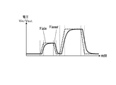
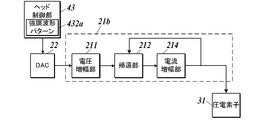
- FIG. 1 is a block diagram illustrating a configuration of an ink jet recording apparatus according to an embodiment of the present invention. It is a figure which shows the example of the waveform pattern of the drive signal input into a drive waveform amplifier circuit, and the drive output signal output. It is a figure which shows the example of the waveform pattern of the drive signal input into a drive waveform amplifier circuit, and the drive output signal output. It is a figure which shows the circuit structure of a drive waveform amplifier circuit. It is a figure which shows the modification of a drive waveform amplifier circuit. It is a figure which shows the modification of a drive waveform amplifier circuit. It is a figure which shows the modification of a drive waveform amplifier circuit. It is a figure which shows the modification of a drive waveform amplifier circuit.
- FIG. 1 is a block diagram showing a functional configuration of an ink jet recording apparatus 1 including a drive waveform amplifier circuit of the present invention.
- the inkjet recording apparatus 1 includes a control unit 41, a movement control unit 42, a movement operation unit 51, a communication unit 52, an operation display unit 53, a notification output unit 54, a head drive control unit 20, and an inkjet head 30. These are connected via a bus 55 so that signals can be transmitted and received.
- the control unit 41 controls the overall operation of the inkjet recording apparatus 1.
- the control unit 41 includes a CPU 411 (Central Processing Unit), a RAM 412 (Random Access Memory), a storage unit 413, and the like.
- the CPU 411 performs various arithmetic processes.
- the CPU 411 reads out a control program stored in the storage unit 413 and performs various control processes related to image recording and setting thereof.
- the RAM 412 provides a working memory space to the CPU 411 and stores temporary data.
- the storage unit 413 includes a non-volatile memory that stores a control program, setting data, and the like. Further, the storage unit 413 may include a DRAM or the like that temporarily stores settings related to a droplet discharge command (print job) acquired from the outside via the communication unit 52, image data to be recorded, and the like.
- the movement operation unit 51 moves a recording medium, which is a target for recording an image, in a predetermined direction to move the recording medium relative to the inkjet head 30, and performs at least operations related to supply and discharge of the recording medium.
- Examples of the moving operation unit 51 include an outer periphery of a cylindrical drum carrying a recording medium on the surface and a rotary motor that rotates around the surface of an endless belt.
- the moving operation unit 51 may be configured to move the recording medium and the inkjet head 30 relative to each other, that is, to move the inkjet head 30 relative to the stationary or moving recording medium.
- the movement control unit 42 operates the movement operation unit 51 to perform a control operation for moving the carried recording medium at an appropriate timing and speed.
- the movement control unit 42 may have a common configuration with the control unit 41.
- the inkjet head 30 is provided with a plurality of nozzles arranged in a predetermined pattern, and records an image on a recording medium by discharging ink droplets from the openings of the plurality of nozzles at an appropriate timing.
- the arrangement pattern of the nozzles is not particularly limited, and may be a one-dimensional array or a two-dimensional array.
- the inkjet head 30 includes a piezoelectric element 31 that is a capacitive load, an ejection selection switching element 32, and the like.
- the piezoelectric element 31 is provided for each of a plurality of nozzles, and is an actuator that discharges liquid droplets from the nozzles by changing the pressure applied to the liquid to be discharged by being deformed according to an applied voltage (drive voltage signal). It is.
- the deformation mode of the piezoelectric element is not particularly limited as long as the applied voltage corresponds to the deformation amount of the piezoelectric element and the pressure applied to the ink changes according to the deformation.
- the ejection selection switching element 32 switches whether each piezoelectric element 31 is supplied with a drive voltage signal from the head drive control unit 20.
- the ejection selection switching element 32 switches the presence / absence of ejection of ink droplets from each nozzle by not supplying a drive voltage signal to the piezoelectric element 31 corresponding to the nozzle that does not eject droplets based on image data to be output. .
- This switching is not limited to the ejection of ink droplets, but is similarly applied to drive voltage signals related to non-ejection waveforms with a small amplitude to the extent that ink droplets are not ejected.
- the head drive control unit 20 outputs a drive voltage signal for driving the piezoelectric element 31 of the inkjet head 30 at an appropriate timing according to each pixel data of the output target image.
- the head drive control unit 20 may be formed collectively on a substrate or the like, or may be arranged dispersedly in each part of the inkjet recording apparatus 1. A part or all of the configuration of the head drive control unit 20 may be provided in the inkjet head 30.
- the head drive control unit 20 includes a head control unit 43, a drive waveform amplification circuit 21, a DAC 22 (digital / analog conversion unit), and the like.
- the DAC 22 converts the waveform pattern data (digital waveform data) of the drive waveform output from the head controller 43 at a predetermined clock frequency into an analog signal, and outputs the obtained analog signal (drive signal) to the drive waveform amplifier circuit 21. To do.
- the drive waveform amplification circuit 21 receives a drive signal having a predetermined waveform pattern from the DAC 22 according to the timing of ink droplet ejection from the nozzles, the non-ejection state type, and the like for each piezoelectric element 31.
- the drive voltage signal amplified by performing the signal amplification operation is output as an output signal.
- a trapezoidal driving voltage signal is applied to the piezoelectric element 31, although not limited thereto.
- the head control unit 43 controls the operation of the head drive control unit 20 in accordance with the presence / absence of image data to be recorded and the content of the image data.
- the head control unit 43 includes a CPU 431, a storage unit 432, and the like.
- the storage unit 432 emphasizes a waveform pattern 432a (information) corresponding to a waveform pattern (predetermined drive waveform) of a drive signal for ejecting ink from the nozzle or vibrating the liquid level (meniscus) of the ink in the nozzle. Are previously stored as digital discrete value array data.
- the CPU 431 applies a driving voltage having an appropriate waveform pattern to the piezoelectric element 31 according to whether or not droplets are ejected from each nozzle based on image data to be recorded stored in the storage unit 432 or the storage unit 413.
- the enhanced waveform pattern data corresponding to the waveform pattern is selected and output to the DAC 22 at an appropriate timing according to a clock signal (synchronization signal) not shown.
- the head control unit 43 may be provided in common with the control unit 41.
- the movement control unit 42 and the head control unit 43 constitute an operation control unit 40 related to image recording.
- the head control unit 43 and the DAC 22 constitute a drive signal generation unit, and the drive signal generation unit and the drive waveform amplification circuit 21 constitute a drive waveform signal output device 20a.
- the communication unit 52 communicates with an external device according to a predetermined communication standard, and transmits and receives data.
- various standards such as LAN (Local Area Network) TCP / IP, near field communication such as wireless LAN, Bluetooth communication (registered trademark: Bluetooth), USB (Universal Serial Bus), etc. It is possible to use direct communication with an external device.
- the communication unit 52 receives a print job which is a command related to image recording from an external device, and outputs status information of the inkjet recording apparatus 1 to the external device as necessary.
- the operation display unit 53 accepts user operations and displays information and menus for the user.
- a display unit provided with an LCD (liquid crystal display) as the display unit 532 is used, and various menus and statuses related to image recording are displayed on the display screen of the LCD.
- a touch panel serving as the operation detection unit 531 is provided corresponding to the LCD, and the touch operation corresponding to the display on the display screen can be detected by arranging the touch panel so as to overlap the display screen of the LCD.
- the operation display unit 53 may include a push button switch and detect a push operation of the push button switch.
- the notification output unit 54 performs a predetermined notification operation when an abnormality occurs in the inkjet recording apparatus 1.
- Examples of the notification output unit 54 include a sound generation unit that generates a predetermined beep sound using a piezoelectric element or the like, and a light emitting unit that blinks or lights an LED lamp.
- pattern data (digital waveform data) corresponding to an appropriate waveform pattern is predetermined from the emphasized waveform pattern 432a stored and held in the storage unit 432 as digital discrete value array data.
- FIG. 2A and 2B are diagrams for explaining the correspondence between the analog signal Vin input from the DAC 22 to the drive waveform amplification circuit 21 and the waveform pattern of the drive output signal Vout output from the drive waveform amplification circuit 21.
- FIG. The analog signal Vin and the drive output signal Vout have different amplitudes at a ratio corresponding to the amplification factor of the voltage, but are shown here with the same amplitude for explanation.
- a drive voltage signal having a drive waveform pattern having different amplitudes depending on the presence / absence of ink discharge or the discharge amount is output alone or in combination within a predetermined period, and the piezoelectric element 31 is output.
- the pressure change with respect to the ink in the nozzle is selectively switched.
- a signal having the same drive waveform pattern as the drive voltage signal of the waveform pattern (initial waveform) originally desired to be applied to the piezoelectric element 31 is to be amplified and output, such as the voltage Vain indicated by the dotted line in FIG. 2A.
- the voltage applied to the piezoelectric element 31 is distorted due to the capacitance of the piezoelectric element 31 and the like, as shown by the solid line Vaout in FIG. 2A, and is delayed from the input signal. The rise and fall will be dull.
- the drive waveform amplification circuit 21 takes into account the actual distortion, that is, the voltage Vbin shown by the dotted line in FIG. Also, a drive signal of a waveform with a sudden change, that is, a waveform pattern (a emphasized waveform pattern) with a voltage change that emphasizes a delay amount and a high frequency component is input. Since the frequency related to the rise and fall dullness has a period (particularly a half cycle) shorter than the time required for the rise and fall, it is necessary for the rise and fall in the initial waveform that is a trapezoidal wave here.
- the emphasized waveform pattern can be generated by emphasizing the higher frequency side with the frequency having a half cycle shorter than time as the lower limit frequency.
- the power spectrum may be adjusted more finely, or instead of preparing an emphasized waveform pattern analytically or numerically, an appropriate waveform may be obtained experimentally, or the voltage Vbin of FIG.
- the rise time and fall time may be shortened from the initial waveform, and a waveform in which an overshoot after the rise and an undershoot after the fall are generated may be roughly drawn.
- Discrete value data of the emphasized waveform pattern 432a is stored in advance in the storage unit 432 (storage step), and an appropriate emphasized waveform pattern 432a is read out during the ink ejection operation by the inkjet head 30, and the analog signal Vin ( Drive signal) and output (drive signal generation step), which is amplified and output by the drive waveform amplification circuit 21 (drive waveform amplification step), so that the finally emphasized component is actually generated.
- a drive voltage signal with a voltage change close to the original drive waveform pattern is applied to the piezoelectric element 31 as shown by the solid line in FIG.
- FIG. 3 is a diagram for explaining a configuration relating to drive waveform amplification in the inkjet recording apparatus 1 of the present embodiment.
- the drive waveform amplifier circuit 21 includes a voltage amplifier 211, a current amplifier 214, and the like.
- the voltage amplification unit 211 amplifies the voltage of the analog signal Vin having the drive waveform input from the DAC 22 to the drive voltage. Since the voltage amplitude of the analog signal Vin output from the DAC 22 is smaller than the actual voltage for driving the piezoelectric element 31, the voltage amplifier 211 amplifies and outputs the amplified voltage.
- the voltage amplification unit 211 includes an OP amplifier A1 (operational amplifier), resistance elements R11 and R13, and the like.
- the OP amplifier A1 is connected to voltages + Vc1 and ⁇ Vc2 corresponding to the amplitude of the drive voltage, and voltage amplification is performed between the voltages + Vc1 and ⁇ Vc2 with an amplification factor according to the resistance ratio of the resistance elements R11 and R13.
- the drive signal subjected to the voltage amplification is sent to the current amplification unit 214 via the resistance element R12.
- the amplitude of the drive voltage is usually as large as several tens of volts (about 30 V to 45 V), and the OP amplifier A1 corresponding to such a high voltage usually has a slew rate and a gain bandwidth (GBW). ) Becomes low, the waveform of the output drive signal tends to become dull.
- the voltage amplitude of the analog signal Vin output from the DAC 22 is set to be larger than that in the past (for example, an amplitude of about 3 V) so that the amplification factor is not excessively increased.
- the current amplifying unit 214 amplifies the power of the driving signal output from the voltage amplifying unit 211, and outputs it as a driving output signal Vout to the piezoelectric element 31 selected by the ejection selection switching element 32 via the resistance element R51. Apply voltage.
- the current amplifying unit 214 includes resistance elements R40 to R46, an N channel FET 41T (field effect transistor), a P channel FET 42T, a capacitor C41, and the like.
- the N-channel FET 41T and the P-channel FET 42T are source followers that output a drive output signal according to the drive signal by a push-pull operation.
- the drive signal input to the current amplifier 214 via the resistance element R40 is divided and input to the gate of the N-channel FET 41T and the gate of the P-channel FET 42T, respectively.
- the input voltage to the gate of the N-channel FET 41T is added with a bias voltage obtained by dividing the potential difference between the power supply voltage Vp and the input voltage by the resistance ratio of the resistance elements R41 and R45, and the input voltage to the gate of the P-channel FET 42T is A bias voltage obtained by dividing the potential difference between the ground voltage and the input voltage by the resistance ratio of the resistance elements R42 and R46 is drawn. Thereby, crossover distortion is avoided.
- the N-channel FET 41T has a drain connected to the power supply voltage Vp, and a source connected to the output terminal via the resistor element R43. The drain of the P-channel FET 42T is grounded, and the source is connected to the output terminal via the resistor element R44.
- the N-channel FET 41T and the P-channel FET 42T are MOSFETs that amplify power (current) and output a voltage signal according to the voltage signal input to each gate terminal.
- the power amplifying unit 214 suppresses the occurrence of thermal runaway due to positive feedback of changes in bias voltage and amplified current accompanying heat generation (temperature rise).
- the capacitor C41 is for stabilizing the power supply voltage Vp, and a capacitor having a larger capacity than other capacitors such as an electrolytic capacitor is preferably used.
- the power supply voltage Vp is equal to or higher than the operating voltage + Vc1 supplied to the OP amplifiers A1 and A2, and is the same here.
- the drive waveform amplifier circuit 21 when the analog signal Vin based on the emphasized waveform pattern is input from the DAC 22 to the drive waveform amplifier circuit 21, the power is amplified and output as the drive output signal Vout.
- the drive output signal Vout is delayed and dull due to the capacitance of the piezoelectric element 31, and the forward and high frequency emphasized portions are canceled out.
- the drive voltage corresponding to the waveform pattern to be originally applied to the piezoelectric element 31 is obtained. Is applied to the piezoelectric element 31.
- the emphasized waveform pattern 432a may be inspected and set before shipment for each inkjet recording apparatus 1 and individually stored in the storage unit 43, or each inkjet recording in which common data is manufactured for a specific inkjet recording apparatus model. You may make it memorize
- [Modification] 4A to 4D are configuration diagrams showing modifications of the drive waveform signal output device 20a of the present embodiment.
- a voltage amplified drive signal is input to a PWM modulation unit 213 (Pulse Width Modulation), and once subjected to pulse width modulation (PWM).
- PWM Pulse Width Modulation
- the demodulator 215 can return the signal to an analog signal.
- a low-pass filter (LPF) using an LC circuit is used as the waveform demodulator 215.
- the drive output signal Vout amplified by the current amplification unit 214 may be negatively fed back to the feedback unit 212.
- the voltage division unit 211 divides the drive output signal Vout according to the voltage amplification factor in the voltage amplification unit 211. You may make negative feedback before. In this case, in order to prevent oscillation due to negative feedback, processing such as suppression of high-frequency signal feedback may be performed using an LPF or the like.
- the emphasized waveform pattern 432a stored in the storage unit 432 is a waveform pattern that takes into account the improvement of the output waveform by negative feedback.
- the storage unit 432 may store a normal waveform pattern and an emphasis parameter 432b used for generating the emphasis waveform pattern instead of storing the emphasis waveform pattern.
- the CPU 431 uses these to perform an enhanced waveform generation process for generating an enhanced waveform pattern, and causes the DAC 22 to output data of the generated enhanced waveform pattern.
- this is more preferable than storing all the emphasized waveform patterns in the storage unit 432. Such a modification may be more efficient.
- the drive waveform signal output device 20a for the inkjet head has a storage unit 432 that stores information related to a predetermined drive waveform, and a predetermined drive based on the information stored in the storage unit 432.
- the head control unit 43 and the DAC 22 as a drive signal generation unit that generates and outputs a waveform drive signal (analog signal Vin), and amplifies the power of the generated drive signal having a predetermined drive waveform to generate a drive output signal Vout.
- a drive waveform amplification circuit 21 that outputs to the piezoelectric element 31 of the inkjet head 30, and the predetermined drive waveform is a capacitance component of the piezoelectric element 31 in an initial waveform pattern set as a voltage waveform to be applied to the piezoelectric element 31.
- This is an emphasized waveform pattern 432a in which a component corresponding to the waveform distortion generated in the drive output signal Vout is emphasized.
- the enhanced waveform pattern 432a in which the distortion is emphasized so that an appropriate drive voltage signal is obtained as a result of the distortion is stored.
- an analog signal Vin is generated from the emphasized waveform pattern 432a and amplified, whereby a drive voltage having a more appropriate waveform pattern is applied to the piezoelectric element 31.
- a drive voltage having a more appropriate waveform pattern is applied to the piezoelectric element 31.
- ink can be discharged from the nozzle with higher accuracy. That is, the drive waveform signal output device 20a can output a drive voltage that enables appropriate ink ejection.
- the drive signal generation unit includes a DAC 22 that converts digital waveform data into an analog signal.
- Information relating to a predetermined drive waveform is digital waveform data of an emphasized waveform pattern, and the digital waveform data is converted into an analog signal by the DAC 22.
- a drive signal having a predetermined drive waveform is generated by the conversion.
- the waveform pattern data that has been emphasized and corrected in order to obtain a drive voltage signal having an appropriate waveform pattern is stored in advance, so that the drive signal of this waveform pattern can be easily and reliably transmitted to the drive waveform amplification circuit 21.
- an appropriate drive voltage signal is finally obtained. Accordingly, appropriate ink ejection can be performed easily and reliably, and the inkjet recording apparatus 1 can perform highly accurate image recording.
- the initial waveform is a trapezoidal wave.
- the predetermined drive waveform emphasizes a high-frequency component of the trapezoidal wave that is equal to or higher than the predetermined lower limit frequency
- drive waveform data and drive waveform signal for obtaining a more appropriate drive voltage signal through easy processing Can be determined.
- the predetermined lower limit frequency is a frequency whose half cycle is shorter than the rise time and fall time of the trapezoidal wave, and emphasizes the high frequency component related to the delay and dullness of the rise and fall due to the capacitive component of the piezoelectric element 31.
- an appropriate drive voltage signal can be easily obtained.
- the predetermined drive waveform is obtained by shortening the rise time and the fall time with respect to the trapezoidal wave, overshooting the voltage at the rise time, and undershooting the voltage at the fall time.
- an appropriate trapezoidal driving voltage signal can be applied to the piezoelectric element 31 when it is affected by the capacitance component of the piezoelectric element 31.
- the inkjet recording apparatus 1 of the present embodiment includes an inkjet head 30 having a nozzle and a piezoelectric element 31 that ejects ink from the nozzle by being deformed according to an applied voltage, and the above-described drive waveform signal output. And a device 20a.
- the ink jet recording apparatus 1 it becomes possible to reduce the influence of the capacitive component of the piezoelectric element 31 and apply an appropriate drive voltage to the piezoelectric element 31, thereby accurately ejecting ink and recording image quality. Can be improved.
- the distortion is emphasized so that an appropriate drive voltage signal can be obtained as a result of the distortion in consideration of the waveform being distorted in advance due to the capacitive component of the piezoelectric element 31.
- a drive voltage having a more appropriate waveform pattern can be applied to the piezoelectric element 31. . Accordingly, it is possible to improve the accuracy of the recorded image by discharging the ink from the nozzle with higher accuracy. That is, according to this drive waveform signal output method, it is possible to output a drive voltage that allows appropriate ink ejection.
- the present invention is not limited to the above-described embodiment, and various modifications can be made.
- the current output is amplified by the push-pull configuration using the MOSFET and the drive output signal Vout is output.
- the current may be amplified by combining bipolar transistors.
- the number of transistors is not limited to two. Three or more transistors may be used, for example, Darlington connection or the like.
- the voltage amplification unit 211 performs voltage amplification by the OP amplifier A1.
- voltage amplification may be performed using a bipolar transistor or the like, or a combination of these may be used in multiple stages. Voltage amplification may be performed.
- the drive waveform signal output device 20a shown in the above embodiment may be manufactured, traded, used, etc. independently of the ink jet recording apparatus 1.
- the trapezoidal wave is described as the initial waveform, but the present invention is not limited to this. It may be a rectangular wave or other waveform.
- the specific details shown in the above embodiment can be appropriately changed without departing from the gist of the present invention.
- the present invention can be used in an inkjet head drive waveform signal output device, an inkjet recording device, and an inkjet head drive waveform signal output method.
Landscapes
- Particle Formation And Scattering Control In Inkjet Printers (AREA)
- Ink Jet (AREA)
Abstract
電力供給部を大型化せずに適切にインクを吐出させることが可能な駆動電圧を出力することの出来るインクジェットヘッドの駆動波形信号出力装置、インクジェット記録装置及びインクジェットヘッドの駆動波形信号出力方法を提供する。駆動波形信号出力装置は、所定の駆動波形に係る強調波形パターン(432a)を記憶する記憶部と、強調波形パターン(432a)に基づいて、所定の駆動波形の駆動信号を生成して出力する駆動信号生成部と、生成された所定の駆動波形の駆動信号の電力を増幅して出力信号としてインクジェットヘッドの圧電素子(31)に出力する駆動波形増幅回路(21)と、を備え、所定の駆動波形は、圧電素子(31)に印加する電圧波形として設定された初期波形のうち、圧電素子(31)の容量成分により出力信号に生じる波形の歪みに応じた成分を強調した強調波形である。
Description
この発明は、インクジェットヘッドの駆動波形信号出力装置、インクジェット記録装置及びインクジェットヘッドの駆動波形信号出力方法に関する。
従来、ノズルからインクを吐出して画像を記録するインクジェット記録装置がある。インクジェット記録装置では、ノズルに連通する圧力室でインクに圧力変化を生じさせることでインクを適宜な形状や液量の液滴としてノズルから吐出させている。インクジェット記録装置において圧力室における圧力変化を生じさせるものとして用いられる一つに圧電素子があり、この圧電素子に適切な電圧を印加して変形量や変形時間を制御する。
しかしながら、圧電素子は、容量性の負荷であり、多数配列されたノズルからのインク吐出有無を各々切り替え、当該切り替えに応じてインクを吐出させるノズルに各々対応する圧電素子に電圧を印加していくと、駆動回路から圧電素子に流れ、また、圧電素子から流出する電荷の総量が電圧印加対象の圧電素子の数に応じて変化することになる。従って、安定的に駆動波形を供給するには、十分な電力供給が必要になり、消費電力が増大するという問題があった。
これに対し、従来、出力信号を帰還させて信号を安定化させる技術がある。特許文献1には、D級増幅した駆動波形信号をLC回路でフィルタリングした出力信号を、位相を進めて帰還させるとともに、微分信号を独立に帰還させることで、電力損失を抑えつつLC回路のフィルタリング周波数を安定的に保ち、適切な波形を出力する技術が開示されている。
しかしながら、インクジェット記録装置におけるノズル数の増加に従って、圧電素子に供給される電流の大きさは、数桁変化する。このような最大電流に合わせて十分な電力を供給可能な電力供給部を用意すると、電力供給部が必要以上に大型化するという課題がある。反対に、電力供給部を大型化させずに高速で駆動波形を印加すると、大きな電流によって出力される駆動波形信号が鈍り、適切にインクが吐出されない場合が生じるという課題がある。
この発明の目的は、電力供給部を大型化せずに適切にインクを吐出させることの出来る駆動電圧を出力可能なインクジェットヘッドの駆動波形信号出力装置、インクジェット記録装置及びインクジェットヘッドの駆動波形信号出力方法を提供することにある。
上記目的を達成するため、請求項1記載の発明は、
所定の駆動波形に係る情報を記憶する記憶部と、
前記記憶部に記憶された前記情報に基づいて、前記所定の駆動波形の駆動信号を生成して出力する駆動信号生成部と、
生成された前記所定の駆動波形の駆動信号の電力を増幅して出力信号としてインクジェットヘッドの容量性負荷に出力する駆動波形増幅回路と、
を備え、
前記所定の駆動波形は、前記容量性負荷に印加する電圧波形として設定された初期波形のうち、前記容量性負荷の容量成分により前記出力信号に生じる波形の歪み成分を強調した強調波形である
ことを特徴とするインクジェットヘッドの駆動波形信号出力装置である。
所定の駆動波形に係る情報を記憶する記憶部と、
前記記憶部に記憶された前記情報に基づいて、前記所定の駆動波形の駆動信号を生成して出力する駆動信号生成部と、
生成された前記所定の駆動波形の駆動信号の電力を増幅して出力信号としてインクジェットヘッドの容量性負荷に出力する駆動波形増幅回路と、
を備え、
前記所定の駆動波形は、前記容量性負荷に印加する電圧波形として設定された初期波形のうち、前記容量性負荷の容量成分により前記出力信号に生じる波形の歪み成分を強調した強調波形である
ことを特徴とするインクジェットヘッドの駆動波形信号出力装置である。
請求項2記載の発明は、請求項1記載のインクジェットヘッドの駆動波形信号出力装置において、
前記駆動信号生成部は、デジタル波形データをアナログ信号に変換するデジタルアナログ変換部を備え、
前記所定の駆動波形に係る情報は、前記強調波形のデジタル波形データであり、当該デジタル波形データが前記デジタルアナログ変換部でアナログ信号に変換されることで前記所定の駆動波形の駆動信号が生成される
ことを特徴としている。
前記駆動信号生成部は、デジタル波形データをアナログ信号に変換するデジタルアナログ変換部を備え、
前記所定の駆動波形に係る情報は、前記強調波形のデジタル波形データであり、当該デジタル波形データが前記デジタルアナログ変換部でアナログ信号に変換されることで前記所定の駆動波形の駆動信号が生成される
ことを特徴としている。
請求項3記載の発明は、請求項1又は2記載のインクジェットヘッドの駆動波形信号出力装置において、
前記初期波形は、台形波であることを特徴としている。
前記初期波形は、台形波であることを特徴としている。
請求項4記載の発明は、請求項3記載のインクジェットヘッドの駆動波形信号出力装置において、
前記所定の駆動波形は、前記台形波のうち所定の下限周波数以上の高周波数成分を強調したものであることを特徴としている。
前記所定の駆動波形は、前記台形波のうち所定の下限周波数以上の高周波数成分を強調したものであることを特徴としている。
請求項5記載の発明は、請求項4記載のインクジェットヘッドの駆動波形信号出力装置において、
前記所定の下限周波数は、前記台形波の立ち上がり時間及び立下がり時間よりも半周期が短い周波数であることを特徴としている。
前記所定の下限周波数は、前記台形波の立ち上がり時間及び立下がり時間よりも半周期が短い周波数であることを特徴としている。
請求項6記載の発明は、請求項3~5の何れか一項に記載のインクジェットヘッドの駆動波形信号出力装置において、
前記所定の駆動波形は、前記台形波に対して立ち上がり時間及び立下がり時間を短縮し、且つ、立ち上がり時の電圧をオーバーシュートさせ、立下がり時の電圧をアンダーシュートさせたものであることを特徴としている。
前記所定の駆動波形は、前記台形波に対して立ち上がり時間及び立下がり時間を短縮し、且つ、立ち上がり時の電圧をオーバーシュートさせ、立下がり時の電圧をアンダーシュートさせたものであることを特徴としている。
請求項7記載の発明は、
ノズルと、印加される電圧に応じて変形することで前記ノズルからインクを吐出させる容量性負荷と、を有するインクジェットヘッドと、
請求項1~6の何れか一項に記載のインクジェットヘッドの駆動波形信号出力装置と、
を備えることを特徴とするインクジェット記録装置である。
ノズルと、印加される電圧に応じて変形することで前記ノズルからインクを吐出させる容量性負荷と、を有するインクジェットヘッドと、
請求項1~6の何れか一項に記載のインクジェットヘッドの駆動波形信号出力装置と、
を備えることを特徴とするインクジェット記録装置である。
請求項8記載の発明は、
所定の駆動波形に係る情報を記憶する記憶ステップ、
前記記憶ステップで記憶された前記情報に基づいて、前記所定の駆動波形の駆動信号を生成して出力する駆動信号生成ステップ、
生成された前記所定の駆動波形の駆動信号の電力を増幅して出力信号としてインクジェットヘッドの容量性負荷に出力する駆動波形増幅ステップ、
を含み、
前記所定の駆動波形は、前記容量性負荷に印加する電圧波形として設定された初期波形のうち、前記容量性負荷の容量に応じて前記出力信号に生じる波形の歪み成分を強調した強調波形である
ことを特徴とするインクジェットヘッドの駆動波形信号出力方法である。
所定の駆動波形に係る情報を記憶する記憶ステップ、
前記記憶ステップで記憶された前記情報に基づいて、前記所定の駆動波形の駆動信号を生成して出力する駆動信号生成ステップ、
生成された前記所定の駆動波形の駆動信号の電力を増幅して出力信号としてインクジェットヘッドの容量性負荷に出力する駆動波形増幅ステップ、
を含み、
前記所定の駆動波形は、前記容量性負荷に印加する電圧波形として設定された初期波形のうち、前記容量性負荷の容量に応じて前記出力信号に生じる波形の歪み成分を強調した強調波形である
ことを特徴とするインクジェットヘッドの駆動波形信号出力方法である。
本発明に従うと、インクジェットヘッドの駆動波形信号出力装置において、電力供給部を大型化せずにインクを適切に吐出させることの可能な駆動電圧を出力することが出来るという効果がある。
以下、本発明の実施の形態を図面に基づいて説明する。
図1は、本発明の駆動波形増幅回路を含むインクジェット記録装置1の機能構成を示すブロック図である。
図1は、本発明の駆動波形増幅回路を含むインクジェット記録装置1の機能構成を示すブロック図である。
インクジェット記録装置1は、制御部41と、移動制御部42と、移動動作部51と、通信部52と、操作表示部53と、報知出力部54と、ヘッド駆動制御部20と、インクジェットヘッド30などを備え、これらは、バス55を介して信号を送受信可能に接続されている。
制御部41は、インクジェット記録装置1の全体動作を統括制御する。制御部41は、CPU411(Central Processing Unit)と、RAM412(Random Access Memory)と、記憶部413などを備える。
CPU411は、各種演算処理を行う。CPU411は、記憶部413に記憶されている制御プログラムを読み出して画像記録やその設定などに係る各種制御処理を行う。
RAM412は、CPU411に作業用のメモリー空間を提供し、一時データを記憶する。
記憶部413は、制御プログラムや設定データなどを記憶する不揮発性メモリーを含む。また、記憶部413は、通信部52を介して外部から取得された液滴吐出命令(プリントジョブ)に係る設定や記録対象の画像データなどを一時的に記憶するDRAMなどを備えても良い。
記憶部413は、制御プログラムや設定データなどを記憶する不揮発性メモリーを含む。また、記憶部413は、通信部52を介して外部から取得された液滴吐出命令(プリントジョブ)に係る設定や記録対象の画像データなどを一時的に記憶するDRAMなどを備えても良い。
移動動作部51は、画像を記録する対象である記録媒体を所定の方向に搬送することでインクジェットヘッド30に対して相対的に移動させ、少なくとも記録媒体の供給及び排出に係る動作を行う。移動動作部51としては、例えば、表面に記録媒体を担持する円筒形状のドラム外周や無端状ベルトの表面を周回動作させる回転モーターなどが挙げられる。なお、移動動作部51は、記録媒体とインクジェットヘッド30とが相対移動させられれば良く、即ち、インクジェットヘッド30を静止又は移動する記録媒体に対して移動させる構成であっても良い。
移動制御部42は、移動動作部51を動作させて、担持されている記録媒体を適切なタイミング及び速度で移動させる制御動作を行う。この移動制御部42は、制御部41と共通の構成であっても良い。
移動制御部42は、移動動作部51を動作させて、担持されている記録媒体を適切なタイミング及び速度で移動させる制御動作を行う。この移動制御部42は、制御部41と共通の構成であっても良い。
インクジェットヘッド30は、複数のノズルが所定のパターンで配列されて設けられ、当該複数のノズルの開口部から適切なタイミングでインクの液滴を吐出させることで記録媒体上に画像を記録する。ノズルの配列パターンは、特には限られず、一次元配列でも二次元配列でも良い。インクジェットヘッド30は、容量性負荷である圧電素子31と、吐出選択スイッチング素子32などを備える。
圧電素子31は、複数のノズルに対して各々設けられ、印加される電圧(駆動電圧信号)に応じて変形して吐出対象の液体にかかる圧力を変化させることでノズルから液滴を吐出させるアクチュエーターである。圧電素子の変形モードは、印加電圧と圧電素子の変形量とが対応し、当該変形に応じてインクに加えられる圧力が変化するモードであれば特には限られない。
吐出選択スイッチング素子32は、各圧電素子31にヘッド駆動制御部20から駆動電圧信号をそれぞれ供給させるか否かを切り替える。吐出選択スイッチング素子32は、出力対象の画像データなどに基づいて液滴を吐出させないノズルに対応する圧電素子31に駆動電圧信号を供給させないことで、各ノズルからのインク液滴の吐出有無を切り替える。また、この切り替えは、インク液滴の吐出に限られず、インク液滴を吐出させない程度に小振幅の非吐出波形に係る駆動電圧信号にも同様に適用される。
ヘッド駆動制御部20は、出力対象画像の各画素データに応じて適切なタイミングでインクジェットヘッド30の圧電素子31を駆動する駆動電圧信号を出力する。ヘッド駆動制御部20は、基板上などにまとめて形成されても良いし、インクジェット記録装置1の各部に分散して配置されていても良い。また、ヘッド駆動制御部20の構成の一部又は全部は、インクジェットヘッド30に設けられていても良い。ヘッド駆動制御部20は、ヘッド制御部43と、駆動波形増幅回路21と、DAC22(デジタルアナログ変換部)などを備える。
DAC22は、ヘッド制御部43から所定のクロック周波数で出力された駆動波形の波形パターンデータ(デジタル波形データ)をアナログ変換して、得られたアナログ信号(駆動信号)を駆動波形増幅回路21に出力する。
駆動波形増幅回路21は、各圧電素子31に対してノズルからのインク液滴吐出タイミングや非吐出の状態種別などに応じて予め定められた波形パターンの駆動信号がそれぞれDAC22から入力され、当該駆動信号の増幅動作を行って増幅された駆動電圧信号を出力信号として出力する。本実施形態のインクジェット記録装置1では、特に限られるものではないが、台形波形状の駆動電圧信号が圧電素子31に対して印加される。
ヘッド制御部43は、記録対象の画像データの有無や画像データの内容に応じてヘッド駆動制御部20の動作を制御する。ヘッド制御部43は、CPU431と、記憶部432などを備える。記憶部432は、ノズルからインクを吐出させたりノズル内のインクの液面(メニスカス)を振動させたりするための駆動信号の波形パターン(所定の駆動波形)に応じた強調波形パターン432a(情報)をデジタル離散値配列データとして予め保持する。CPU431は、記憶部432又は記憶部413に記憶された記録対象の画像データに基づいて、各ノズルから液滴を吐出させるか否かなどに従って圧電素子31に適切な波形パターンの駆動電圧を印加させるための当該波形パターンに応じた強調波形パターンデータを選択し、図示略のクロック信号(同期信号)に応じた適切なタイミングでDAC22に出力する。
このヘッド制御部43は、制御部41と共通に設けられても良い。
移動制御部42とヘッド制御部43とにより画像記録に係る動作制御部40が構成される。また、ヘッド制御部43とDAC22とにより駆動信号生成部が構成され、この駆動信号生成部と駆動波形増幅回路21とにより駆動波形信号出力装置20aが構成される。
このヘッド制御部43は、制御部41と共通に設けられても良い。
移動制御部42とヘッド制御部43とにより画像記録に係る動作制御部40が構成される。また、ヘッド制御部43とDAC22とにより駆動信号生成部が構成され、この駆動信号生成部と駆動波形増幅回路21とにより駆動波形信号出力装置20aが構成される。
通信部52は、外部機器との間で所定の通信規格に従って通信し、データの送受信を行う。用いられる通信規格としては、LAN(Local Area Network)によるTCP/IPなどの各種規格の他、無線LAN、ブルートゥース通信(登録商標:Bluetooth)などの近距離無線通信や、USB(Universal Serial Bus)などによる外部機器との直接通信を用いることが可能である。通信部52は、外部機器から画像記録に係る命令であるプリントジョブを受信し、必要に応じて外部機器に対してインクジェット記録装置1のステータス情報などを出力する。
操作表示部53は、ユーザー操作を受け付けたりユーザーに情報やメニューなどを示すための表示を行なったりする。操作表示部53としては、例えば、表示部532としてのLCD(液晶ディスプレイ)を備えたものが用いられ、当該LCDの表示画面上に画像記録に係る各種メニューやステータスなどを表示させる。また、このLCDに対応して操作検出部531としてのタッチパネルを備え、このタッチパネルをLCDの表示画面上に重ねて配置することで当該表示画面へ表示に応じたタッチ操作を検出可能としている。或いは、操作表示部53は、押しボタンスイッチを備え、当該押しボタンスイッチの押下操作を検出しても良い。
報知出力部54は、インクジェット記録装置1に異常が生じた場合などに所定の報知動作を行う。報知出力部54としては、例えば、圧電素子などを用いて所定のビープ音を発生させる音声発生部やLEDランプを点滅又は点灯させる発光部などが挙げられる。
次に、本実施形態のインクジェット記録装置1の駆動波形増幅回路21について説明する。
本実施形態のインクジェット記録装置1では、上述のように、デジタル離散値配列データとして記憶部432に記憶保持された強調波形パターン432aから適切な波形パターンに応じたパターンデータ(デジタル波形データ)を所定のクロック周波数に従ってヘッド制御部43から出力し、これをDAC22でアナログ変換(D/A変換)したのち、駆動波形増幅回路21で電力(電圧、次いで電流)を増幅して各圧電素子31に出力する。
本実施形態のインクジェット記録装置1では、上述のように、デジタル離散値配列データとして記憶部432に記憶保持された強調波形パターン432aから適切な波形パターンに応じたパターンデータ(デジタル波形データ)を所定のクロック周波数に従ってヘッド制御部43から出力し、これをDAC22でアナログ変換(D/A変換)したのち、駆動波形増幅回路21で電力(電圧、次いで電流)を増幅して各圧電素子31に出力する。
図2A及び図2Bは、DAC22から駆動波形増幅回路21へ入力されるアナログ信号Vinと、駆動波形増幅回路21から出力される駆動出力信号Voutの波形パターンとの対応関係を説明する図である。なお、アナログ信号Vinと駆動出力信号Voutとでは、電圧の増幅率に応じた比率で振幅が異なるが、ここでは説明のために同じ振幅で示している。
本実施形態のインクジェット記録装置1では、インクの吐出有無や吐出量などに応じて異なる振幅を有する駆動波形パターンの駆動電圧信号を所定周期内で単独で又は組み合わせて出力して、圧電素子31を変形動作させることで、ノズル内のインクに対する圧力変化を選択的に切り替える。このとき、図2Aの点線で示す電圧Vainのように、本来圧電素子31に対して印加したい波形パターン(初期波形)の駆動電圧信号と同一の駆動波形パターンの信号を増幅して出力しようとすると、実際には、図2Aの実線で示す電圧Vaoutのように、圧電素子31の容量などによって当該圧電素子31に印加される電圧には歪みが生じ、入力信号よりも遅延し、また、電圧の立ち上がりや立下がりが鈍ることになる。
これに対し、この駆動波形増幅回路21には、これら実際に生じるこの歪み、即ち、遅延や鈍りの大きさを考慮して、図2Bの点線で示す電圧Vbinのように、本来の印加電圧よりも急激な変化を伴う波形、即ち、遅延分や高周波数成分を強調した電圧変化を伴う波形パターン(強調波形パターン)の駆動信号を入力させる。立ち上がりや立下がりの鈍り具合に係る周波数は、当該立ち上がりや立下がりに要する時間より短い周期(特に半周期)のものであるので、ここでは、台形波である初期波形において立ち上がり及び立下がりに要する時間よりも半周期が短い周波数を下限周波数としてこれよりも高周波数側を強調して強調波形パターンを生成しておくことが出来る。又は、より細かくパワースペクトルを調整しても良いし、或いは、解析的又は数値的に強調波形パターンを準備するのではなく、実験的に適切な波形を得たり、或いは、図2Bの電圧Vbinのように、立ち上がり時間や立下がり時間を初期波形より短縮し、且つ立ち上がり後のオーバーシュートや立下がり後のアンダーシュートを生じさせた波形を大雑把に描いたりしても良い。この強調波形パターン432aの離散値データを記憶部432に予め記憶させておき(記憶ステップ)、インクジェットヘッド30によるインク吐出動作時には、適切な強調波形パターン432aが読み出されてDAC22によりアナログ信号Vin(駆動信号)に変換されて出力され(駆動信号生成ステップ)、これが駆動波形増幅回路21で増幅されて出力される(駆動波形増幅ステップ)ことで、最終的に強調された成分が実際に生じた遅延や鈍りと相殺されて、図2Bの実線で示す電圧Vboutのように、本来の駆動波形パターンに近い電圧変化を伴う駆動電圧信号が圧電素子31に印加される。
図3は、本実施形態のインクジェット記録装置1における駆動波形の増幅に係る構成を説明する図である。
駆動波形増幅回路21は、電圧増幅部211と、電流増幅部214などを備える。
電圧増幅部211は、DAC22から入力された駆動波形のアナログ信号Vinの電圧を駆動電圧にまで増幅する。DAC22から出力されるアナログ信号Vinの電圧振幅は、圧電素子31を駆動する実際の電圧よりも小さいので、電圧増幅部211は、これを増幅して出力する。
電圧増幅部211は、OPアンプA1(オペアンプ)と、抵抗素子R11及びR13などを有する。OPアンプA1は、駆動電圧の振幅に対応した電圧+Vc1、-Vc2に接続されて、当該電圧+Vc1、-Vc2の間で抵抗素子R11、R13の抵抗比に応じた増幅率で電圧増幅が行われる。電圧増幅がなされた駆動信号は、抵抗素子R12を介して電流増幅部214に送られる。なお、インクジェットヘッド30では、駆動電圧の振幅が通常では数十ボルト(約30V~45Vなど)と大きく、このような高電圧に対応するOPアンプA1は、通常、スルーレートや利得帯域幅(GBW)が低くなるので、出力される駆動信号の波形が鈍りやすい。インクジェット記録装置1では、増幅率を大きくし過ぎないようにDAC22から出力されるアナログ信号Vinの電圧振幅を従来(例えば3V程度の振幅)に比して大きく定めるのが好ましい。また、ここでは、+Vc1>0、-Vc2<0である。
電流増幅部214は、電圧増幅部211から出力された駆動信号の電力を増幅し、駆動出力信号Voutとして吐出選択スイッチング素子32により選択された圧電素子31に対して抵抗素子R51を介して出力、電圧を印加する。電流増幅部214は、抵抗素子R40~R46と、NチャンネルFET41T(電界効果トランジスター)と、PチャンネルFET42Tと、キャパシターC41などを備える。
NチャンネルFET41T及びPチャンネルFET42Tは、プッシュプル動作により駆動信号に従った駆動出力信号を出力するソースフォロワーである。
電流増幅部214に抵抗素子R40を介して入力された駆動信号は、分割されてそれぞれNチャンネルFET41Tのゲート及びPチャンネルFET42Tのゲートに入力される。NチャンネルFET41Tのゲートへの入力電圧は、電源電圧Vpと入力電圧との電位差が抵抗素子R41、R45の抵抗比で分圧されたバイアス電圧が加算され、PチャンネルFET42Tのゲートへの入力電圧は、接地電圧と入力電圧との電位差が抵抗素子R42、R46の抵抗比で分圧されたバイアス電圧が引かれる。これにより、クロスオーバー歪みが回避されている。NチャンネルFET41Tは、ドレインが電源電圧Vpに接続され、ソースが抵抗素子R43を介して出力端に接続されている。PチャンネルFET42Tは、ドレインが接地され、ソースが抵抗素子R44を介して出力端に接続されている。
電流増幅部214に抵抗素子R40を介して入力された駆動信号は、分割されてそれぞれNチャンネルFET41Tのゲート及びPチャンネルFET42Tのゲートに入力される。NチャンネルFET41Tのゲートへの入力電圧は、電源電圧Vpと入力電圧との電位差が抵抗素子R41、R45の抵抗比で分圧されたバイアス電圧が加算され、PチャンネルFET42Tのゲートへの入力電圧は、接地電圧と入力電圧との電位差が抵抗素子R42、R46の抵抗比で分圧されたバイアス電圧が引かれる。これにより、クロスオーバー歪みが回避されている。NチャンネルFET41Tは、ドレインが電源電圧Vpに接続され、ソースが抵抗素子R43を介して出力端に接続されている。PチャンネルFET42Tは、ドレインが接地され、ソースが抵抗素子R44を介して出力端に接続されている。
NチャンネルFET41T及びPチャンネルFET42Tは、各ゲート端子に入力される電圧信号に従った電圧の信号を電力(電流)増幅して出力するMOSFETである。バイポーラートランジスターの代わりにMOSFETを用いることで、電力増幅部214では、発熱(温度上昇)に伴ってバイアス電圧や増幅電流の変化が正帰還することによる熱暴走の発生を抑える。
キャパシターC41は、電源電圧Vpの安定用のものであり、電解コンデンサーなど他のキャパシターと比較して容量が大きいものが好ましく用いられる。電源電圧Vpは、OPアンプA1、A2に供給する動作電圧+Vc1以上であり、ここでは同一である。
キャパシターC41は、電源電圧Vpの安定用のものであり、電解コンデンサーなど他のキャパシターと比較して容量が大きいものが好ましく用いられる。電源電圧Vpは、OPアンプA1、A2に供給する動作電圧+Vc1以上であり、ここでは同一である。
上述のように、強調波形パターンに基づくアナログ信号VinがDAC22から駆動波形増幅回路21に入力されると、電力増幅されて駆動出力信号Voutとして出力される。この駆動出力信号Voutには、圧電素子31の容量により遅延及び鈍りが生じ、前倒し及び高周波強調された部分が相殺されて、結果的に本来圧電素子31に印加すべき波形パターンに応じた駆動電圧が圧電素子31に印加されることになる。
強調波形パターン432aは、インクジェット記録装置1ごとに出荷前に検査設定して個別に記憶部43に記憶させても良いし、特定のインクジェット記録装置の機種について共通のデータを製造された各インクジェット記録装置1の記憶部43にそれぞれ記憶させても良い。また、複数種類のデータを予め記憶部43に記憶させ、出荷前検査時などにインクジェット記録装置1について適切なデータを選択設定可能としても良い。
[変形例]
図4A~図4Dは、本実施形態の駆動波形信号出力装置20aの変形例を示す構成図である。
図4Aに示すように、駆動波形増幅回路21aにおいて、電圧増幅された駆動信号をPWM変調部213(Pulse Width Modulation)に入力させて一度パルス幅変調(PWM)し、電流増幅を行った後に波形復調部215でアナログ信号に戻して出力させることが出来る。波形復調部215としては、例えば、LC回路による低域通過フィルター(LPF)などが用いられる。
図4A~図4Dは、本実施形態の駆動波形信号出力装置20aの変形例を示す構成図である。
図4Aに示すように、駆動波形増幅回路21aにおいて、電圧増幅された駆動信号をPWM変調部213(Pulse Width Modulation)に入力させて一度パルス幅変調(PWM)し、電流増幅を行った後に波形復調部215でアナログ信号に戻して出力させることが出来る。波形復調部215としては、例えば、LC回路による低域通過フィルター(LPF)などが用いられる。
また、図4Bに示すように、駆動波形増幅回路21bにおいて、電流増幅部214で電力増幅された駆動出力信号Voutを帰還部212に負帰還させることとしても良い。ここでは、電圧増幅部211と電流増幅部214との間に負帰還させる例を示したが、駆動出力信号Voutのうち電圧増幅部211における電圧増幅率に応じた分圧を電圧増幅部211の前に負帰還させても良い。この場合、負帰還による発振などを防ぐために、LPFなどを用いて高周波数帯の信号の帰還を抑制するなどの処理を行っても良い。また、記憶部432に記憶される強調波形パターン432aは、負帰還による出力波形の改善などを考慮した波形パターンとなる。
また、図4Cに示すように、記憶部432には、強調波形パターンを記憶させる代わりに通常の波形パターン及び強調波形パターンの生成に用いる強調パラメーター432bを記憶させても良い。CPU431がこれらを用いて強調波形パターンを生成する強調波形生成処理を行って、当該生成された強調波形パターンのデータをDAC22に出力させる。パラメーター設定のみで強調波形パターンの生成が可能な場合であって、出力画像などに応じてパラメーター設定を適宜変更する場合などには、全ての強調波形パターンを記憶部432に記憶させるよりも、このような変形例のほうが効率良い場合があり得る。
以上のように、本実施形態のインクジェットヘッドの駆動波形信号出力装置20aは、所定の駆動波形に係る情報を記憶する記憶部432と、記憶部432に記憶された情報に基づいて、所定の駆動波形の駆動信号(アナログ信号Vin)を生成して出力する駆動信号生成部としてのヘッド制御部43及びDAC22と、生成された所定の駆動波形の駆動信号の電力を増幅して駆動出力信号Voutとしてインクジェットヘッド30の圧電素子31に出力する駆動波形増幅回路21と、を備え、所定の駆動波形は、圧電素子31に印加する電圧波形として設定された初期波形パターンのうち、圧電素子31の容量成分により駆動出力信号Voutに生じる波形の歪みに応じた成分を強調した強調波形パターン432aである。
このように、予め圧電素子31の容量成分の影響で波形が歪むことを考慮して、当該歪みの結果、適切な駆動電圧信号が得られるように歪み分を強調した強調波形パターン432aを記憶しておき、この強調波形パターン432aからアナログ信号Vinを生成し、これを増幅することで、容易且つより適切な波形パターンの駆動電圧が圧電素子31に印加される。これにより、より精度良くノズルからインクを吐出させることが出来る。即ち、この駆動波形信号出力装置20aは、適切なインク吐出が可能な駆動電圧を出力することが出来る。
このように、予め圧電素子31の容量成分の影響で波形が歪むことを考慮して、当該歪みの結果、適切な駆動電圧信号が得られるように歪み分を強調した強調波形パターン432aを記憶しておき、この強調波形パターン432aからアナログ信号Vinを生成し、これを増幅することで、容易且つより適切な波形パターンの駆動電圧が圧電素子31に印加される。これにより、より精度良くノズルからインクを吐出させることが出来る。即ち、この駆動波形信号出力装置20aは、適切なインク吐出が可能な駆動電圧を出力することが出来る。
また、駆動信号生成部は、デジタル波形データをアナログ信号に変換するDAC22を備え、所定の駆動波形に係る情報は、強調波形パターンのデジタル波形データであり、当該デジタル波形データがDAC22でアナログ信号に変換されることで所定の駆動波形の駆動信号が生成される。
このように、適切な波形パターンの駆動電圧信号を得るために強調補正された波形パターンのデータを予め保持しておくことで、容易且つ確実にこの波形パターンの駆動信号が駆動波形増幅回路21に入力されて、最終的に適切な駆動電圧信号が得られる。従って、適切なインク吐出が容易且つ確実に行われて、インクジェット記録装置1では、精度の高い画像記録を行うことが出来る。
このように、適切な波形パターンの駆動電圧信号を得るために強調補正された波形パターンのデータを予め保持しておくことで、容易且つ確実にこの波形パターンの駆動信号が駆動波形増幅回路21に入力されて、最終的に適切な駆動電圧信号が得られる。従って、適切なインク吐出が容易且つ確実に行われて、インクジェット記録装置1では、精度の高い画像記録を行うことが出来る。
また、初期波形は、台形波である。このように立ち上がりや立下がりの期間が明瞭な波形に対して本発明を適用することで、容易且つより効果的に適切な駆動電圧信号が得られ、これにより、より正確なインクの吐出が可能になる。
また、所定の駆動波形は、台形波のうち所定の下限周波数以上の高周波数成分を強調したものであるので、容易な処理でより適切な駆動電圧信号を得るための駆動波形データや駆動波形信号を定めることが出来る。
また、所定の下限周波数は、台形波の立ち上がり時間及び立下がり時間よりも半周期が短い周波数であり、圧電素子31の容量成分による立ち上がりや立下がりの遅延や鈍りに係る高周波数成分を強調することで、簡便に適切な駆動電圧信号を得ることが出来る。
また、所定の駆動波形は、台形波に対して立ち上がり時間及び立下がり時間を短縮し、且つ、立ち上がり時の電圧をオーバーシュートさせ、立下がり時の電圧をアンダーシュートさせたものである。具体的にこのような波形を予め設定しておくことで、圧電素子31の容量成分による影響を受けたときに適切な台形波形状の駆動電圧信号を圧電素子31に印加することが出来る。
また、本実施形態のインクジェット記録装置1は、ノズルと、印加される電圧に応じて変形することでノズルからインクを吐出させる圧電素子31と、を有するインクジェットヘッド30と、上述の駆動波形信号出力装置20aと、を備える。
このインクジェット記録装置1では、圧電素子31の容量成分の影響を低減して適切な駆動電圧を圧電素子31に印加することが可能になり、これにより、正確にインクを吐出して記録画像の画質を向上させることが出来る。
このインクジェット記録装置1では、圧電素子31の容量成分の影響を低減して適切な駆動電圧を圧電素子31に印加することが可能になり、これにより、正確にインクを吐出して記録画像の画質を向上させることが出来る。
また、上述の駆動波形信号出力方法では、予め圧電素子31の容量成分の影響で波形が歪むことを考慮して、当該歪みの結果、適切な駆動電圧信号が得られるように歪み分を強調した強調波形パターン432aを記憶しておき、この強調波形パターン432aからアナログ信号Vinを生成し、これを増幅することで、容易且つより適切な波形パターンの駆動電圧が圧電素子31に印加することが出来る。これにより、より精度良くノズルからインクを吐出させて、記録画像の精度を向上させることが出来る。即ち、この駆動波形信号出力方法によれば、適切なインク吐出が可能な駆動電圧を出力することが出来る。
なお、本発明は、上記実施の形態に限られるものではなく、様々な変更が可能である。
例えば、上記実施の形態では、MOSFETを用いてプッシュプル型の構成により電流増幅を行って駆動出力信号Voutを出力したが、バイポーラー型のトランジスターが組み合わされて電流の増幅を行っても良い。また、トランジスターの数は2つに限られない。3つ以上のトランジスターが用いられて、例えば、ダーリントン接続などがなされていても良い。
例えば、上記実施の形態では、MOSFETを用いてプッシュプル型の構成により電流増幅を行って駆動出力信号Voutを出力したが、バイポーラー型のトランジスターが組み合わされて電流の増幅を行っても良い。また、トランジスターの数は2つに限られない。3つ以上のトランジスターが用いられて、例えば、ダーリントン接続などがなされていても良い。
また、上記実施の形態では、電圧増幅部211において、OPアンプA1により電圧増幅を行ったが、バイポーラートランジスターなどを用いて電圧の増幅を行っても良く、或いは、これらを組み合わせて多段階で電圧増幅を行っても良い。
また、上記実施の形態で示した駆動波形信号出力装置20aは、インクジェット記録装置1とは独立して製造、取引、使用などがなされても良い。
また、上記実施の形態では、台形波を初期波形として説明したが、これに限るものではない。矩形波やその他の波形であっても良い。
その他、上記実施の形態で示した具体的な細部は、本発明の趣旨を逸脱しない範囲において適宜変更可能である。
その他、上記実施の形態で示した具体的な細部は、本発明の趣旨を逸脱しない範囲において適宜変更可能である。
この発明は、インクジェットヘッドの駆動波形信号出力装置、インクジェット記録装置及びインクジェットヘッドの駆動波形信号出力方法に利用することができる。
1 インクジェット記録装置
20 ヘッド駆動制御部
20a 駆動波形信号出力装置
21、21a、21b 駆動波形増幅回路
211 電圧増幅部
212 帰還部
213 PWM変調部
214 電流増幅部
215 波形復調部
30 インクジェットヘッド
31 圧電素子
32 吐出選択スイッチング素子
40 動作制御部
41 制御部
411 CPU
412 RAM
413 記憶部
42 移動制御部
43 ヘッド制御部
431 CPU
432 記憶部
51 移動動作部
52 通信部
53 操作表示部
531 操作検出部
532 表示部
54 報知出力部
55 バス
A1、A2 OPアンプ
C21、C31、C41 キャパシター
41T NチャンネルFET
42T PチャンネルFET
R11、R12、R21、R31、R41~R44、R51 抵抗素子
20 ヘッド駆動制御部
20a 駆動波形信号出力装置
21、21a、21b 駆動波形増幅回路
211 電圧増幅部
212 帰還部
213 PWM変調部
214 電流増幅部
215 波形復調部
30 インクジェットヘッド
31 圧電素子
32 吐出選択スイッチング素子
40 動作制御部
41 制御部
411 CPU
412 RAM
413 記憶部
42 移動制御部
43 ヘッド制御部
431 CPU
432 記憶部
51 移動動作部
52 通信部
53 操作表示部
531 操作検出部
532 表示部
54 報知出力部
55 バス
A1、A2 OPアンプ
C21、C31、C41 キャパシター
41T NチャンネルFET
42T PチャンネルFET
R11、R12、R21、R31、R41~R44、R51 抵抗素子
Claims (8)
- 所定の駆動波形に係る情報を記憶する記憶部と、
前記記憶部に記憶された前記情報に基づいて、前記所定の駆動波形の駆動信号を生成して出力する駆動信号生成部と、
生成された前記所定の駆動波形の駆動信号の電力を増幅して出力信号としてインクジェットヘッドの容量性負荷に出力する駆動波形増幅回路と、
を備え、
前記所定の駆動波形は、前記容量性負荷に印加する電圧波形として設定された初期波形のうち、前記容量性負荷の容量成分により前記出力信号に生じる波形の歪みに応じた成分を強調した強調波形である
ことを特徴とするインクジェットヘッドの駆動波形信号出力装置。 - 前記駆動信号生成部は、デジタル波形データをアナログ信号に変換するデジタルアナログ変換部を備え、
前記所定の駆動波形に係る情報は、前記強調波形のデジタル波形データであり、当該デジタル波形データが前記デジタルアナログ変換部でアナログ信号に変換されることで前記所定の駆動波形の駆動信号が生成される
ことを特徴とする請求項1記載のインクジェットヘッドの駆動波形信号出力装置。 - 前記初期波形は、台形波であることを特徴とする請求項1又は2記載のインクジェットヘッドの駆動波形信号出力装置。
- 前記所定の駆動波形は、前記台形波のうち所定の下限周波数以上の高周波数成分を強調したものであることを特徴とする請求項3記載のインクジェットヘッドの駆動波形信号出力装置。
- 前記所定の下限周波数は、前記台形波の立ち上がり時間及び立下がり時間よりも半周期が短い周波数であることを特徴とする請求項4記載のインクジェットヘッドの駆動波形信号出力装置。
- 前記所定の駆動波形は、前記台形波に対して立ち上がり時間及び立下がり時間を短縮し、且つ、立ち上がり時の電圧をオーバーシュートさせ、立下がり時の電圧をアンダーシュートさせたものであることを特徴とする請求項3~5の何れか一項に記載のインクジェットヘッドの駆動波形信号出力装置。
- ノズルと、印加される電圧に応じて変形することで前記ノズルからインクを吐出させる容量性負荷と、を有するインクジェットヘッドと、
請求項1~6の何れか一項に記載のインクジェットヘッドの駆動波形信号出力装置と、
を備えることを特徴とするインクジェット記録装置。 - 所定の駆動波形に係る情報を記憶する記憶ステップ、
前記記憶ステップで記憶された前記情報に基づいて、前記所定の駆動波形の駆動信号を生成して出力する駆動信号生成ステップ、
生成された前記所定の駆動波形の駆動信号の電力を増幅して出力信号としてインクジェットヘッドの容量性負荷に出力する駆動波形増幅ステップ、
を含み、
前記所定の駆動波形は、前記容量性負荷に印加する電圧波形として設定された初期波形のうち、前記容量性負荷の容量に応じて前記出力信号に生じる波形の歪み成分を強調した強調波形である
ことを特徴とするインクジェットヘッドの駆動波形信号出力方法。
Priority Applications (1)
| Application Number | Priority Date | Filing Date | Title |
|---|---|---|---|
| JP2018522385A JPWO2017212865A1 (ja) | 2016-06-09 | 2017-05-12 | インクジェットヘッドの駆動波形信号出力装置、インクジェット記録装置及びインクジェットヘッドの駆動波形信号出力方法 |
Applications Claiming Priority (2)
| Application Number | Priority Date | Filing Date | Title |
|---|---|---|---|
| JP2016-114933 | 2016-06-09 | ||
| JP2016114933 | 2016-06-09 |
Publications (1)
| Publication Number | Publication Date |
|---|---|
| WO2017212865A1 true WO2017212865A1 (ja) | 2017-12-14 |
Family
ID=60577835
Family Applications (1)
| Application Number | Title | Priority Date | Filing Date |
|---|---|---|---|
| PCT/JP2017/017974 Ceased WO2017212865A1 (ja) | 2016-06-09 | 2017-05-12 | インクジェットヘッドの駆動波形信号出力装置、インクジェット記録装置及びインクジェットヘッドの駆動波形信号出力方法 |
Country Status (2)
| Country | Link |
|---|---|
| JP (1) | JPWO2017212865A1 (ja) |
| WO (1) | WO2017212865A1 (ja) |
Cited By (2)
| Publication number | Priority date | Publication date | Assignee | Title |
|---|---|---|---|---|
| CN114683699A (zh) * | 2020-12-29 | 2022-07-01 | 精工爱普生株式会社 | 液体喷出装置 |
| CN114683700A (zh) * | 2020-12-29 | 2022-07-01 | 精工爱普生株式会社 | 液体喷出装置 |
Families Citing this family (1)
| Publication number | Priority date | Publication date | Assignee | Title |
|---|---|---|---|---|
| CN114603996B (zh) * | 2022-02-11 | 2024-02-13 | 大连理工大学 | 一种压电喷墨打印头的驱动电压波形确定方法 |
Citations (3)
| Publication number | Priority date | Publication date | Assignee | Title |
|---|---|---|---|---|
| JP2003025566A (ja) * | 2001-07-13 | 2003-01-29 | Hitachi Koki Co Ltd | インクジェット印字装置の圧電素子の制御方法 |
| US20030025770A1 (en) * | 2000-03-31 | 2003-02-06 | Fujitsu Limited | Multi-nozzle ink jet head |
| JP2005169737A (ja) * | 2003-12-09 | 2005-06-30 | Ricoh Co Ltd | 駆動波形生成回路、駆動波形生成方法および画像形成装置 |
Family Cites Families (2)
| Publication number | Priority date | Publication date | Assignee | Title |
|---|---|---|---|---|
| JP2003053969A (ja) * | 2001-08-10 | 2003-02-26 | Hitachi Koki Co Ltd | インクジェットヘッドの駆動制御方法 |
| JP5653925B2 (ja) * | 2008-11-05 | 2015-01-14 | オセ−テクノロジーズ ビーブイ | インクジェットプリンタのプリントヘッドを駆動するドライバ回路 |
-
2017
- 2017-05-12 JP JP2018522385A patent/JPWO2017212865A1/ja active Pending
- 2017-05-12 WO PCT/JP2017/017974 patent/WO2017212865A1/ja not_active Ceased
Patent Citations (3)
| Publication number | Priority date | Publication date | Assignee | Title |
|---|---|---|---|---|
| US20030025770A1 (en) * | 2000-03-31 | 2003-02-06 | Fujitsu Limited | Multi-nozzle ink jet head |
| JP2003025566A (ja) * | 2001-07-13 | 2003-01-29 | Hitachi Koki Co Ltd | インクジェット印字装置の圧電素子の制御方法 |
| JP2005169737A (ja) * | 2003-12-09 | 2005-06-30 | Ricoh Co Ltd | 駆動波形生成回路、駆動波形生成方法および画像形成装置 |
Cited By (4)
| Publication number | Priority date | Publication date | Assignee | Title |
|---|---|---|---|---|
| CN114683699A (zh) * | 2020-12-29 | 2022-07-01 | 精工爱普生株式会社 | 液体喷出装置 |
| CN114683700A (zh) * | 2020-12-29 | 2022-07-01 | 精工爱普生株式会社 | 液体喷出装置 |
| CN114683699B (zh) * | 2020-12-29 | 2023-06-13 | 精工爱普生株式会社 | 液体喷出装置 |
| CN114683700B (zh) * | 2020-12-29 | 2023-06-20 | 精工爱普生株式会社 | 液体喷出装置 |
Also Published As
| Publication number | Publication date |
|---|---|
| JPWO2017212865A1 (ja) | 2019-04-04 |
Similar Documents
| Publication | Publication Date | Title |
|---|---|---|
| US8353568B2 (en) | Inkjet head driving apparatus with multi pulse generator | |
| JP5577811B2 (ja) | 容量性負荷駆動装置、液体噴射装置およびウォーターパルスメス | |
| US8240798B2 (en) | Head drive apparatus of inkjet printer and inkjet printer | |
| US8398194B2 (en) | Power amplifier and liquid jet printing apparatus | |
| JP6662380B2 (ja) | 記録ヘッドの駆動回路及び画像記録装置 | |
| JP4572722B2 (ja) | 液体吐出装置、及び、液体吐出方法 | |
| WO2017212865A1 (ja) | インクジェットヘッドの駆動波形信号出力装置、インクジェット記録装置及びインクジェットヘッドの駆動波形信号出力方法 | |
| JP5163207B2 (ja) | 液体噴射装置、及び印刷装置 | |
| JP2016107445A (ja) | 液体吐出装置、ヘッドユニット、容量性負荷駆動用集積回路装置、容量性負荷駆動回路及び液体吐出装置の製造方法 | |
| JP6911848B2 (ja) | インクジェットヘッドの駆動波形増幅回路、インクジェット記録装置及びインクジェットヘッドの駆動波形増幅方法 | |
| WO2011024307A1 (ja) | インクジェットプリンタ及び印刷方法 | |
| JP2002283565A (ja) | インクジェット式プリンタのヘッド駆動装置及び駆動方法 | |
| CN101112815A (zh) | 一种根据温度调整电压波形的方法及系统 | |
| US7638992B2 (en) | Drive power control device, liquid ejection apparatus, and drive power control method | |
| EP3984752B1 (en) | Drive circuit of recording head and image recorder | |
| CN108973329B (zh) | 液体喷出装置以及印刷装置 | |
| JP2006076084A (ja) | インクジェット記録装置 | |
| JP4433709B2 (ja) | インクジェットヘッドの駆動回路 | |
| KR100403581B1 (ko) | 잉크젯 헤드 구동 회로 | |
| JP5440684B2 (ja) | 駆動回路 | |
| JP2026022725A (ja) | 駆動回路、インクジェットヘッド及びインクジェット記録装置 | |
| JP2015042262A (ja) | 制御装置および流体噴射装置 | |
| JP2009178925A (ja) | 容量性負荷駆動回路、液体噴射ヘッド及び液体吐出装置 | |
| JPH1120155A (ja) | 記録装置用ヘッド駆動装置 | |
| JP5045936B2 (ja) | 容量性負荷の駆動回路及び液体吐出装置 |
Legal Events
| Date | Code | Title | Description |
|---|---|---|---|
| ENP | Entry into the national phase |
Ref document number: 2018522385 Country of ref document: JP Kind code of ref document: A |
|
| 121 | Ep: the epo has been informed by wipo that ep was designated in this application |
Ref document number: 17810047 Country of ref document: EP Kind code of ref document: A1 |
|
| NENP | Non-entry into the national phase |
Ref country code: DE |
|
| 122 | Ep: pct application non-entry in european phase |
Ref document number: 17810047 Country of ref document: EP Kind code of ref document: A1 |