WO2017212554A1 - Dc/dcコンバータ - Google Patents
Dc/dcコンバータ Download PDFInfo
- Publication number
- WO2017212554A1 WO2017212554A1 PCT/JP2016/066960 JP2016066960W WO2017212554A1 WO 2017212554 A1 WO2017212554 A1 WO 2017212554A1 JP 2016066960 W JP2016066960 W JP 2016066960W WO 2017212554 A1 WO2017212554 A1 WO 2017212554A1
- Authority
- WO
- WIPO (PCT)
- Prior art keywords
- power supply
- phase
- output power
- load
- supply wiring
- Prior art date
- Legal status (The legal status is an assumption and is not a legal conclusion. Google has not performed a legal analysis and makes no representation as to the accuracy of the status listed.)
- Ceased
Links
Images




Classifications
-
- H—ELECTRICITY
- H02—GENERATION; CONVERSION OR DISTRIBUTION OF ELECTRIC POWER
- H02M—APPARATUS FOR CONVERSION BETWEEN AC AND AC, BETWEEN AC AND DC, OR BETWEEN DC AND DC, AND FOR USE WITH MAINS OR SIMILAR POWER SUPPLY SYSTEMS; CONVERSION OF DC OR AC INPUT POWER INTO SURGE OUTPUT POWER; CONTROL OR REGULATION THEREOF
- H02M3/00—Conversion of DC power input into DC power output
- H02M3/02—Conversion of DC power input into DC power output without intermediate conversion into AC
- H02M3/04—Conversion of DC power input into DC power output without intermediate conversion into AC by static converters
- H02M3/10—Conversion of DC power input into DC power output without intermediate conversion into AC by static converters using discharge tubes with control electrode or semiconductor devices with control electrode
- H02M3/145—Conversion of DC power input into DC power output without intermediate conversion into AC by static converters using discharge tubes with control electrode or semiconductor devices with control electrode using devices of a triode or transistor type requiring continuous application of a control signal
- H02M3/155—Conversion of DC power input into DC power output without intermediate conversion into AC by static converters using discharge tubes with control electrode or semiconductor devices with control electrode using devices of a triode or transistor type requiring continuous application of a control signal using semiconductor devices only
- H02M3/156—Conversion of DC power input into DC power output without intermediate conversion into AC by static converters using discharge tubes with control electrode or semiconductor devices with control electrode using devices of a triode or transistor type requiring continuous application of a control signal using semiconductor devices only with automatic control of output voltage or current, e.g. switching regulators
- H02M3/158—Conversion of DC power input into DC power output without intermediate conversion into AC by static converters using discharge tubes with control electrode or semiconductor devices with control electrode using devices of a triode or transistor type requiring continuous application of a control signal using semiconductor devices only with automatic control of output voltage or current, e.g. switching regulators including plural semiconductor devices as final control devices for a single load
- H02M3/1584—Conversion of DC power input into DC power output without intermediate conversion into AC by static converters using discharge tubes with control electrode or semiconductor devices with control electrode using devices of a triode or transistor type requiring continuous application of a control signal using semiconductor devices only with automatic control of output voltage or current, e.g. switching regulators including plural semiconductor devices as final control devices for a single load with a plurality of power processing stages connected in parallel
-
- H—ELECTRICITY
- H02—GENERATION; CONVERSION OR DISTRIBUTION OF ELECTRIC POWER
- H02M—APPARATUS FOR CONVERSION BETWEEN AC AND AC, BETWEEN AC AND DC, OR BETWEEN DC AND DC, AND FOR USE WITH MAINS OR SIMILAR POWER SUPPLY SYSTEMS; CONVERSION OF DC OR AC INPUT POWER INTO SURGE OUTPUT POWER; CONTROL OR REGULATION THEREOF
- H02M1/00—Details of apparatus for conversion
- H02M1/0003—Details of control, feedback or regulation circuits
- H02M1/0009—Devices or circuits for detecting current in a converter
-
- H—ELECTRICITY
- H02—GENERATION; CONVERSION OR DISTRIBUTION OF ELECTRIC POWER
- H02M—APPARATUS FOR CONVERSION BETWEEN AC AND AC, BETWEEN AC AND DC, OR BETWEEN DC AND DC, AND FOR USE WITH MAINS OR SIMILAR POWER SUPPLY SYSTEMS; CONVERSION OF DC OR AC INPUT POWER INTO SURGE OUTPUT POWER; CONTROL OR REGULATION THEREOF
- H02M3/00—Conversion of DC power input into DC power output
- H02M3/003—Constructional details, e.g. physical layout, assembly, wiring or busbar connections
-
- H—ELECTRICITY
- H02—GENERATION; CONVERSION OR DISTRIBUTION OF ELECTRIC POWER
- H02M—APPARATUS FOR CONVERSION BETWEEN AC AND AC, BETWEEN AC AND DC, OR BETWEEN DC AND DC, AND FOR USE WITH MAINS OR SIMILAR POWER SUPPLY SYSTEMS; CONVERSION OF DC OR AC INPUT POWER INTO SURGE OUTPUT POWER; CONTROL OR REGULATION THEREOF
- H02M3/00—Conversion of DC power input into DC power output
- H02M3/02—Conversion of DC power input into DC power output without intermediate conversion into AC
- H02M3/04—Conversion of DC power input into DC power output without intermediate conversion into AC by static converters
- H02M3/10—Conversion of DC power input into DC power output without intermediate conversion into AC by static converters using discharge tubes with control electrode or semiconductor devices with control electrode
- H02M3/145—Conversion of DC power input into DC power output without intermediate conversion into AC by static converters using discharge tubes with control electrode or semiconductor devices with control electrode using devices of a triode or transistor type requiring continuous application of a control signal
- H02M3/155—Conversion of DC power input into DC power output without intermediate conversion into AC by static converters using discharge tubes with control electrode or semiconductor devices with control electrode using devices of a triode or transistor type requiring continuous application of a control signal using semiconductor devices only
- H02M3/156—Conversion of DC power input into DC power output without intermediate conversion into AC by static converters using discharge tubes with control electrode or semiconductor devices with control electrode using devices of a triode or transistor type requiring continuous application of a control signal using semiconductor devices only with automatic control of output voltage or current, e.g. switching regulators
- H02M3/158—Conversion of DC power input into DC power output without intermediate conversion into AC by static converters using discharge tubes with control electrode or semiconductor devices with control electrode using devices of a triode or transistor type requiring continuous application of a control signal using semiconductor devices only with automatic control of output voltage or current, e.g. switching regulators including plural semiconductor devices as final control devices for a single load
- H02M3/1584—Conversion of DC power input into DC power output without intermediate conversion into AC by static converters using discharge tubes with control electrode or semiconductor devices with control electrode using devices of a triode or transistor type requiring continuous application of a control signal using semiconductor devices only with automatic control of output voltage or current, e.g. switching regulators including plural semiconductor devices as final control devices for a single load with a plurality of power processing stages connected in parallel
- H02M3/1586—Conversion of DC power input into DC power output without intermediate conversion into AC by static converters using discharge tubes with control electrode or semiconductor devices with control electrode using devices of a triode or transistor type requiring continuous application of a control signal using semiconductor devices only with automatic control of output voltage or current, e.g. switching regulators including plural semiconductor devices as final control devices for a single load with a plurality of power processing stages connected in parallel switched with a phase shift, i.e. interleaved
Definitions
- the present invention relates to a DC / DC converter.
- DC / DC converters switching regulators
- switching regulators are used in electronic devices such as laptops, desktop computers, game machines, tablet PCs, and smart phones to step down a certain level of DC voltage to an optimum level for the load.
- a multi-phase converter is used as a power source for a high-performance processor.
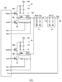
- FIG. 1 is a circuit diagram showing a multi-phase DC / DC converter 100r. This DC / DC converter is operated by connecting two channels in parallel and shifting the phase. As a result, the pseudo apparent switching frequency is increased, and the load fluctuation of the processor operating at high speed can be followed at high speed.
- the DC / DC converter 100 r receives the input voltage Vin at the input terminal 102, steps down the input voltage Vin, generates an output voltage Vout stabilized at a predetermined target voltage, and loads such as a processor connected to the output terminal 104 ( (Not shown).
- the DC / DC converter 100r includes two phases, and includes an input capacitor Ci, a high side transistor MH, a low side transistor ML, and an inductor L for each phase. Each circuit element has a subscript indicating a phase number.
- the outputs of the plurality of phases ⁇ 1 and ⁇ 2 are connected in common, and the common connection point 108 and the output terminal 104 are connected via an output power supply wiring 110.
- a smoothing capacitor Cs is connected to the output power wiring 110 at a position near the common connection point 108, and a decoupling capacitor Cd is connected at a position near the output terminal 104.
- the smoothing capacitor Cs and the decoupling capacitor Cd may be a bulk capacitor (Bulk-Cap) and a multilayer ceramic capacitor (MLCC), respectively.
- the output voltage Vout is fed back to the sense pin (Vsen) of the controller 120.
- the controller 120 performs feedback control on the multiple phases ⁇ 1 and ⁇ 2 so that the output voltage Vout approaches the target voltage Vref.
- the controller 120 monitors the coil current Icoil flowing through the inductor L of each phase in addition to the output voltage Vout in order to uniformly operate a plurality of phases or for overcurrent protection.
- the controller 120 detects the coil current Icoil based on the potential difference between the Isen + and Isen ⁇ pins, that is, the voltage drop of the current sense resistor CSR i .
- FIG. 2 is a circuit diagram showing another multi-phase DC / DC converter 100s.
- the current sensing method is different from that of FIG. 1, the current sensing resistor CSR of FIG. 1 is omitted, and the DC resistance (parasitic series resistance) DCR of the inductor L is used instead.
- the A related technique is described in Patent Document 2. Specifically, in each phase ⁇ i , a CR filter 106 is provided in parallel with the inductor L i, and voltages at both ends of the capacitor are input to the Isen + and Isen ⁇ pins of the controller 120.
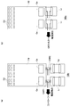
- FIG. 3A is a diagram showing a layout of the DC / DC converter of FIG. 1
- FIG. 3B is a diagram showing a layout of the DC / DC converter of FIG.
- the current sense resistor CSR has a small manufacturing variation in resistance value and a small temperature dependency, and therefore, highly accurate current detection is possible. Since the voltage drop indicates the coil current Icoil, the detection circuit can be configured simply. On the other hand, the current sense resistor CSR, which is a chip component, is expensive, and as shown in FIG. 3A, there is a problem that the number of components and the mounting area increase in relation to the chip component. Further, since the current sense resistor CSR is lost, there is a problem that efficiency is lowered and transient characteristics are deteriorated.
- the present invention has been made in view of these problems, and one of the exemplary purposes of an aspect thereof is to provide a DC / DC converter that solves the problems of the conventional current detection method.
- An aspect of the present invention relates to an N-phase (N is an integer of 2 or more) multi-phase DC / DC converter.
- the DC / DC converter includes a high-side transistor, a low-side transistor, and an inductor provided for each phase, and output power supply wiring that connects a load side end of each of the N inductors and the load.
- the output power supply wiring branches from the load toward the load side end of the N inductors, and the coil current flowing through the inductor of each phase is based on the voltage drop of the branch portion corresponding to the phase of the output power supply wiring. Detected.
- the mounting area can be reduced, the efficiency can be improved, and good transient characteristics can be realized.
- the detection circuit can be simple.
- the output power supply wiring is located farther from the inductor than the high-side and low-side transistors, which are heat generating elements. Therefore, temperature dependency can be reduced and high-precision current detection can be achieved compared to the case where the internal resistance of the inductor is used. Is possible.
- the voltage detection point on the load side of the branch portion may be shared for two adjacent phases of the N phase. Thereby, wiring can be simplified compared with the case where a voltage drop is detected with two terminals for each branch portion.
- the resistance values of the N branch parts of the N phase may be equal. Thereby, the signal processing in the controller of the DC / DC converter can be simplified.
- the output power supply wiring defines an unbranched virtual power supply wiring that connects the load side end of each of the N inductors and the load, a slit is made in the virtual power supply wiring from between adjacent inductors toward the load. You may have a shape.
- a first output capacitor for each phase may be connected to each of the N branches of the output power supply wiring.
- a common second output capacitor may be connected to the merging portion on the load side of the output power supply wiring in all phases.
- the output power supply wiring is multilayer wiring and may be branched in each layer. By making it multilayer, the impedance of the output power supply wiring can be lowered. In addition, for each phase, the coil current can be detected by using the resistance value of the combined impedance of the branch portions of the same phase of a plurality of layers.
- the coil current of each phase can be detected.
- FIG. 3A is a diagram showing a layout of the DC / DC converter of FIG. 1
- FIG. 3B is a diagram showing a layout of the DC / DC converter of FIG. 1 is a circuit diagram of an N-phase multi-phase DC / DC converter according to an embodiment.
- FIG. 6 is a partial layout diagram of a DC / DC converter according to a first modification. It is a layout diagram of a part of a 4-phase DC / DC converter.
- the state in which the member A is connected to the member B means that the member A and the member B are physically directly connected, or the member A and the member B are electrically connected.
- the case where it is indirectly connected through other members that do not affect the state or inhibit the function is also included.
- the state in which the member C is provided between the member A and the member B refers to the case where the member A and the member C or the member B and the member C are directly connected, as well as an electrical condition. This includes cases where the connection is indirectly made through other members that do not affect the connection state or inhibit the function.
- FIG. 4 is a circuit diagram of an N-phase (N is an integer of 2 or more) multi-phase DC / DC converter 100 according to the embodiment.
- N 2 is set for ease of understanding and simplification of description.
- the DC / DC converter 100 receives an input voltage Vin at its input terminal 102, steps down the voltage to generate an output voltage Vout stabilized at a predetermined target voltage, and a load such as a processor connected to the output terminal 104 200.
- the DC / DC converter 100 includes a high-side transistor MH, a low-side transistor ML and an inductor L provided for each phase ⁇ , a controller 120, an output power supply wiring 130, several input capacitors Ci, and several output capacitors Cs and Cd. Is provided.
- the output power supply wiring 130 connects the load side end of each of the N inductors L 1 to L N and the load 200.
- the output power supply line 130 branches from the load 200 toward the load side ends of the N inductors L 1 to L N.
- N branch portions br 1 to br N corresponding to the N phase are merged on the load side.
- the output power supply wiring 130 includes a printed wiring formed on the printed circuit board.
- first output capacitors Cs 1 to Cs N for each phase are connected to the N branch portions br 1 to br N of the output power supply wiring 130, respectively.
- Each first output capacitor Cs i may be a bulk capacitor and is connected to the upstream (inductor side) end of the corresponding branch portion br i .
- a common second output capacitor Cd in all phases is connected to the confluence portion on the load 200 side of the output power supply wiring 130.
- the second output capacitor Cd may be a multilayer ceramic capacitor.
- the voltages at both ends (voltage detection points) of the branch portion br 1 of the first phase ⁇ 1 are input to the Isen + 1 and Isen-1 pins of the controller 120, and both ends (voltage detection) of the branch portion br 2 of the second phase ⁇ 2.
- the voltage of the point) is input to the Isen + 2 and Isen-2 pins of the controller 120.
- the coil current Icoil i flowing through the inductor L i of the i-th phase ⁇ i is detected based on the voltage drop Vs i of the branch portion br i corresponding to the phase ⁇ i of the output power wiring 130.
- the correction coefficient ⁇ may be introduced and the coil current Icoil i may be calculated based on the equation (3).
- Icoil i Vs i / ( ⁇ ⁇ R i ) (3)
- a resistance value corresponding to ⁇ ⁇ R i may be calculated based on simulation or the like or may be actually measured.
- the DC resistances R 1 to R N of each phase are preferably equal. Thereby, the process which correct
- the above is the configuration of the DC / DC converter 100.
- the DC / DC converter 100 of FIG. 4 since the current sense resistor CSR is unnecessary compared with the DC / DC converter 100R of FIG. 1, the cost can be reduced, the mounting area can be reduced, and the efficiency can be improved. Good transient characteristics can be realized.
- the voltage drop Vs of the branch part br is proportional to the coil current Icoil, it can be handled in the same way as the current sense resistor CSR of the DC / DC converter 100R of FIG. 1, and the detection circuit can be simple. Furthermore, since the output power supply wiring 130 is located farther from the inductor L than the high-side transistor MH and the low-side transistor ML, which are heating elements, temperature dependency can be reduced as compared with the case where the DC resistance DCR of the inductor L is used. Highly accurate current detection is possible.
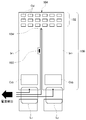
- FIG. 5 is a diagram showing a layout on the printed board of the DC / DC converter 100 of FIG.
- the output power supply wiring 130 has a plurality of branch portions br 1 to br 2 , which are joined at the output terminal 104 side (load 200).
- the output power supply wiring 130 is a single-layer wiring.
- the first output capacitors Cs 1 and Cs 2 are connected to the upstream ends of the corresponding branch portions br 1 and br 2 , respectively.
- a plurality of second output capacitors Cd that are common in all phases are connected to the confluence portion 132 on the load 200 side of the output power supply wiring 130.
- one end of each of the first output capacitor Cs and the second output capacitor Cd is connected not to the output power supply wiring 130 but to the ground wiring (ground plane).
- the connection with the ground wiring is omitted.
- the voltage detection points 134 on the load side of the two branch portions br 1 and br 2 are shared by the two adjacent phases ⁇ 1 and ⁇ 2 of the N phases.
- the branch portions br 2 on the load side of the voltage measuring points 134 and upstream (inductor L 2) in accordance with the voltage drop between the voltage detection points 138 of the side, the coil current Icoil 2 of the second phase phi 2 is detected.
- the sense wiring 140 When a voltage drop is detected at two terminals for each of the branch portions br 1 and br 2 , four sense wirings 140 drawn from the voltage detection point are required.
- the wiring 140 can be reduced to three, and the configuration can be simplified.
- the sense wiring 140 may be formed in the same wiring layer as the output power supply wiring 130 or may be formed in a different wiring layer.
- the output power line 130 are formed symmetrically with multi-phase, therefore, the resistance value R 1, R 2 branches of the N partial br 1, br 2 are equal. Thereby, the signal processing in the controller of the DC / DC converter can be simplified.
- the output power supply wiring 110 is not divided for each phase, and the first output capacitor (smoothing capacitor) Cs is also common to all phases.
- the output power supply wiring 130 is branched for each phase, so that the coil current of each channel can be measured.
- the output power supply wiring 130 has a shape in which a slit 142 is inserted into the virtual power supply wiring 110 from between the adjacent inductors L 1 and L 2 toward the load (output terminal 104). Although the straight slit 142 is shown in FIG. 5, the present invention is not limited to this, and it may be bent or may include a curved line.
- the DC resistances R 1 and R 2 of the branch portions br 1 and br 2 can be designed according to the width and shape of the slit 142.
- FIG. 6 is a diagram illustrating another example of the output power supply wiring 130. Since the output power supply wiring 130 is required to have a low impedance, it is designed as widely as possible. However, the width on the output terminal 104 side is restricted by the pin arrangement of the load 200. Therefore, as shown in FIG. 6, the width of the output power supply wiring 130 tapers so as to become narrower as it approaches the output terminal 104.
- two branch portions br 1 and br 2 can be formed by defining the virtual power supply wiring 110 and inserting a slit 142 in the virtual power supply wiring 110. And by trial and error based on the simulation and / or measured, and DC resistance R 1 between the voltage measuring points 134 and voltage measuring points 136, the DC resistance R 2 between the voltage measuring points 134 and the voltage detecting point 138 is equal Thus, the shape and position of the slit 142 are optimized.
- the voltage detection point 134 is provided in the vicinity of the apex of the slit 142, the sense wiring 140 can be routed using the slit 142 portion.
- the present invention is not limited to this, and the voltage detection point 134 may be provided at any location of the joining portion 132.
- the output power wiring 130 often has copper as a main component, and its resistivity has temperature dependence. As described above, since the output power supply wiring 130 is separated from the high-side transistor MH and the low-side transistor ML that are heating elements, it can be said that the output power wiring 130 is hardly affected by the temperature change, but the heat generation of the processor that is the load is large. There is a possibility that the DC resistances R 1 and R 2 of the branch portions br 1 and br 2 of the output power supply wiring 130 have temperature dependence that cannot be ignored.
- FIG. 7 is a partial layout diagram of the DC / DC converter 100a according to the first modification.
- the DC / DC converter 100a includes a temperature sensor 150 that measures the temperature of the branch portions br 1 and br 2 of the output power supply wiring 130.
- the temperature sensor 150 can be a thermistor or a thermocouple.
- the temperature sensor 150 is preferably disposed in the slit 142 portion of the output power supply wiring 130, and can detect the temperatures of both the branch portions br 1 and br 2 .
- a temperature detection signal that is an output of the temperature sensor 150 is input to the controller 120.
- the controller 120 corrects the DC resistances R 1 and R 2 based on the temperature detection signal. Thereby, the temperature dependence of the current detection accuracy can be improved.
- FIG. 8 is a layout diagram of a part of the 4-phase DC / DC converter 100b.
- the output power supply wiring 130b includes a merging portion 132 and four branch portions br 1 to br 4 corresponding to four phases.
- a slit 142 is formed between two adjacent branch portions br.
- the voltage detection points 134 on the output terminal 104 side of the branch portions br 1 and br 2 are shared, and the voltage detection point 135 on the output terminal 104 side of the branch portions br 3 and br 4 is shared.
- the output power supply wiring 130 has been described as a single-layer wiring in the embodiment, it may be a multilayer wiring. In this case, the output power supply wiring 130 may be branched in each layer.
- the multilayer structure can reduce the impedance of the output power supply wiring 130.
- the coil current can be detected by using the resistance value of the combined impedance of the branch portions of the same phase of a plurality of layers.
- the present invention can be used for a power supply circuit.
Landscapes
- Engineering & Computer Science (AREA)
- Power Engineering (AREA)
- Dc-Dc Converters (AREA)
Abstract
電流センス抵抗を不要とすることで、実装面積を小さく、また効率を改善でき、良好なトランジェント特性を実現できるDC/DCコンバータを提供することを課題とする。 Nフェーズ(Nは2以上の整数)のマルチフェーズDC/DCコンバータ100が提供される。ハイサイドトランジスタMH、ローサイドトランジスタMLおよびインダクタLは、フェーズφごとに設けられる。出力電源配線130は、N個のインダクタL1~LNそれぞれの負荷側端と負荷200を接続する。出力電源配線130は、負荷200からN個のインダクタL1~LNの負荷側端に向かって枝分かれしている。第iフェーズφi(i=1,2,…N)のインダクタLiに流れるコイル電流が、出力電源配線130の当該フェーズφiに対応する枝部分briの電圧降下Vsiにもとづいて検出される。
Description
本発明は、DC/DCコンバータに関する。
ラップトップあるいはデスクトップコンピュータ、ゲーム専用機、タブレットPCやスマートホンなどの電子機器において、あるレベルの直流電圧を、負荷に最適なレベルに降圧するためのDC/DCコンバータ(スイッチングレギュレータ)が利用される。また高性能なプロセッサの電源として、マルチフェーズコンバータが用いられている。
図1は、マルチフェーズDC/DCコンバータ100rを示す回路図である。このDC/DCコンバータは、2チャンネルを並列接続し、位相をずらして動作させる。これにより、擬似的な見かけ上のスイッチング周波数を高め、高速動作するプロセッサの負荷変動に高速に追従可能となる。
DC/DCコンバータ100rは、入力端子102に入力電圧Vinを受け、それを降圧し、所定の目標電圧に安定化された出力電圧Voutを生成し、出力端子104に接続されるプロセッサなどの負荷(不図示)に供給する。
DC/DCコンバータ100rは、2フェーズで構成され、各フェーズごとに、入力キャパシタCi、ハイサイドトランジスタMH、ローサイドトランジスタML、インダクタLを有している。各回路素子には、フェーズ番号を示す下付の添え字が付されている。複数フェーズφ1,φ2の出力は共通に接続され、共通接続点108と出力端子104の間は、出力電源配線110を介して接続される。出力電源配線110には、共通接続点108に近い位置に平滑キャパシタCsが接続され、出力端子104に近い位置に、デカップリングキャパシタCdが接続される。平滑キャパシタCs、デカップリングキャパシタCdはそれぞれ、バルクコンデンサ(Bulk-Cap)、積層セラミックコンデンサ(MLCC)であってもよい。
出力電圧Voutは、コントローラ120のセンスピン(Vsen)にフィードバックされる。コントローラ120は、出力電圧Voutが目標電圧Vrefに近づくように、複数フェーズφ1,φ2をフィードバック制御する。
コントローラ120は、複数のフェーズを均一動作させるために、あるいは過電流保護のために、出力電圧Voutに加えて、各フェーズのインダクタLに流れるコイル電流Icoilを監視している。
図1のDC/DCコンバータ100rでは、各フェーズφiにおいて、インダクタLiと直列に電流センス抵抗CSRiが挿入されており、電流センス抵抗CSRiの両端それぞれの電圧が、コントローラ120のIsen+,Isen-ピンに入力されている。コントローラ120は、Isen+,Isen-ピンの電位差、すなわち電流センス抵抗CSRiの電圧降下にもとづいて、コイル電流Icoilを検出する。
図2は、別のマルチフェーズDC/DCコンバータ100sを示す回路図である。このDC/DCコンバータ100sでは、電流センスの方式が図1のそれと異なっており、図1の電流センス抵抗CSRが省略され、その代わりに、インダクタLの直流抵抗(寄生直列抵抗)DCRが利用される。関連する技術は、特許文献2に記載される。具体的には各フェーズφiにおいて、インダクタLiと並列にCRフィルタ106が設けられ、キャパシタの両端それぞれの電圧が、コントローラ120のIsen+,Isen-ピンに入力されている。
本発明者は、図1あるいは図2のDC/DCコンバータについて検討した結果、以下の課題を認識するに至った。図3(a)は、図1のDC/DCコンバータの、図3(b)は、図2のDC/DCコンバータのプリント基板上のレイアウトを示す図である。
図1の電流検出方式において、電流センス抵抗CSRは、抵抗値の製造バラツキが小さく、また温度依存性が小さいため、高精度な電流検出が可能となる。またその電圧降下がコイル電流Icoilを示すため、検出回路がシンプルに構成できる。その反面、チップ部品である電流センス抵抗CSRは高価であり、また図3(a)に示すように、チップ部品に関連して、部品点数および実装面積が増大するという問題がある。また電流センス抵抗CSRが損失となるため、効率の低下を招き、トランジェント特性が悪化するという問題がある。
図2の電流検出方式では、電流センス抵抗CSRが不要であるため、図3(b)に示すように、実装面積を小さくでき、またコストを下げることができる。また、電流センス抵抗CSRに起因する損失が無いため、効率、トランジェント特性の観点で優れている。一方で、この方式は、インダクタLの抵抗DCRのばらつきが大きく、また温度依存性が大きいため、電流検出精度の観点で劣っている。またCRフィルタ106が必要であることから、検出回路の構成が複雑となってしまう。
本発明はこれらの課題に鑑みてなされたものであり、そのある態様の例示的な目的のひとつは、従来の電流検出方式の問題を解決したDC/DCコンバータの提供にある。
本発明のある態様は、Nフェーズ(Nは2以上の整数)のマルチフェーズDC/DCコンバータに関する。DC/DCコンバータは、フェーズごとに設けられたハイサイドトランジスタ、ローサイドトランジスタおよびインダクタと、N個のインダクタそれぞれの負荷側端と負荷を接続する出力電源配線と、を備える。出力電源配線は、負荷からN個のインダクタの負荷側端に向かって枝分かれしており、各フェーズのインダクタに流れるコイル電流が、出力電源配線の当該フェーズに対応する枝部分の電圧降下にもとづいて検出される。
この態様によると、電流センス抵抗が不要であるため、実装面積を小さく、また効率を改善でき、良好なトランジェント特性を実現できる。また枝部分の電圧降下は、コイル電流に比例するため、検出回路もシンプルで済む。さらに出力電源配線は、発熱素子であるハイサイドトランジスタ、ローサイドトランジスタから、インダクタよりも遠い箇所に位置するため、インダクタの内部抵抗を用いる場合よりも、温度依存性を低減でき、高精度な電流検出が可能となる。
Nフェーズのうち隣接する2フェーズに関して、枝部分の負荷側の電圧検出点が共通化されていてもよい。これにより、枝部分ごとに2端子で電圧降下を検出する場合に比べて、配線を簡素化できる。
NフェーズのN個の枝部分の抵抗値は等しくてもよい。これにより、DC/DCコンバータのコントローラにおける信号処理が簡素化できる。
出力電源配線は、N個のインダクタそれぞれの負荷側端と負荷を接続する枝分かれのない仮想電源配線を規定したとき、当該仮想電源配線に、隣接するインダクタの間から負荷に向かってスリットを入れた形状を有してもよい。
出力電源配線のN個の枝部分にはそれぞれ、フェーズごとの第1出力キャパシタが接続されてもよい。出力電源配線の負荷側の合流部分には、全フェーズで共通の第2出力キャパシタが接続されてもよい。
出力電源配線は多層配線であり、各層において分岐していてもよい。多層化することで、出力電源配線のインピーダンスを下げることができる。またフェーズごとに、複数の層の同じフェーズの枝部分の合成インピーダンスの抵抗値を利用して、コイル電流を検出できる。
なお、以上の構成要素の任意の組合せ、本発明の表現を、方法、装置、システムなどの間で変換したものもまた、本発明の態様として有効である。
本発明によれば、各フェーズのコイル電流を検出できる。
以下、本発明を好適な実施の形態をもとに図面を参照しながら説明する。各図面に示される同一または同等の構成要素、部材、処理には、同一の符号を付するものとし、適宜重複した説明は省略する。また、実施の形態は、発明を限定するものではなく例示であって、実施の形態に記述されるすべての特徴やその組み合わせは、必ずしも発明の本質的なものであるとは限らない。
本明細書において、「部材Aが、部材Bと接続された状態」とは、部材Aと部材Bが物理的に直接的に接続される場合や、部材Aと部材Bが、電気的な接続状態に影響を及ぼさず、あるいは機能を阻害しない他の部材を介して間接的に接続される場合も含む。
同様に、「部材Cが、部材Aと部材Bの間に設けられた状態」とは、部材Aと部材C、あるいは部材Bと部材Cが直接的に接続される場合のほか、電気的な接続状態に影響を及ぼさず、あるいは機能を阻害しない他の部材を介して間接的に接続される場合も含む。
図4は、実施の形態に係るNフェーズ(Nは2以上の整数)のマルチフェーズDC/DCコンバータ100の回路図である。本実施の形態では理解の容易化、説明の簡潔化のため、N=2とする。DC/DCコンバータ100は、その入力端子102に入力電圧Vinを受け、それを降圧して所定の目標電圧に安定化された出力電圧Voutを生成し、出力端子104に接続されるプロセッサなどの負荷200に供給する。
DC/DCコンバータ100は、フェーズφごとに設けられたハイサイドトランジスタMH、ローサイドトランジスタMLおよびインダクタLと、コントローラ120、出力電源配線130、いくつかの入力キャパシタCiおよびいくつかの出力キャパシタCs,Cdを備える。
出力電源配線130は、N個のインダクタL1~LNそれぞれの負荷側端と負荷200を接続する。出力電源配線130は、負荷200からN個のインダクタL1~LNの負荷側端に向かって枝分かれしている。言い換えればNフェーズに対応するN本の枝部分br1~brNが、負荷側において合流している。後述するように出力電源配線130は、プリント基板に形成されるプリント配線を含む。
本実施の形態において、出力電源配線130のN個の枝部分br1~brNにはそれぞれ、フェーズごとの第1出力キャパシタCs1~CsNが接続される。各第1出力キャパシタCsiは、バルクキャパシタであってもよく、対応する枝部分briの上流側(インダクタ側)の端部に接続される。また出力電源配線130の負荷200側の合流部分には、全フェーズで共通の第2出力キャパシタCdが接続される。第2出力キャパシタCdは積層セラミックコンデンサであってもよい。
第1フェーズφ1の枝部分br1の両端(電圧検出点)それぞれの電圧は、コントローラ120のIsen+1,Isen-1ピンに入力され、第2フェーズφ2の枝部分br2の両端(電圧検出点)の電圧は、コントローラ120のIsen+2,Isen-2ピンに入力される。そして第iフェーズφiのインダクタLiに流れるコイル電流Icoiliは、出力電源配線130の当該フェーズφiに対応する枝部分briの電圧降下Vsiにもとづいて検出される。
第iフェーズφiの枝部分briのインピーダンス(直流抵抗)をRiとすると、その電圧降下Vsiは、式(1)で与えられる。各枝部分briの直流抵抗Riは、プリント基板の配線の寄生抵抗に相当する。
Vsi=Ri×Icoili …(1)
したがって直流抵抗Riをあらかじめ測定し、あるいはシミュレーションによって計算しておくことにより、式(2)にしたがい電圧降下Vsiにもとづいてコイル電流Icoiliを検知できる。
Icoili=Vsi/Ri …(2)
Vsi=Ri×Icoili …(1)
したがって直流抵抗Riをあらかじめ測定し、あるいはシミュレーションによって計算しておくことにより、式(2)にしたがい電圧降下Vsiにもとづいてコイル電流Icoiliを検知できる。
Icoili=Vsi/Ri …(2)
なお出力電源配線130の形状によっては、電圧検出点134を通過せずに負荷200に流れ込む電流も若干存在する。この場合、補正係数αを導入し、式(3)にもとづいてコイル電流Icoiliを計算してもよい。
Icoili=Vsi/(α×Ri) …(3)
あるいはα×Riに相当する抵抗値をシミュレーション等にもとづいて計算し、あるいは実測してもよい。
Icoili=Vsi/(α×Ri) …(3)
あるいはα×Riに相当する抵抗値をシミュレーション等にもとづいて計算し、あるいは実測してもよい。
各フェーズの直流抵抗R1~RNは等しいことが好ましい。これにより、コントローラ120において抵抗値を補正する処理が不要となる。
以上がDC/DCコンバータ100の構成である。図4のDC/DCコンバータ100によれば、図1のDC/DCコンバータ100Rと比べて、電流センス抵抗CSRが不要であるため、低コスト化でき、実装面積を小さくし、また効率を改善でき、良好なトランジェント特性を実現できる。
また枝部分brの電圧降下Vsは、コイル電流Icoilに比例するため、図1のDC/DCコンバータ100Rの電流センス抵抗CSRと同等に扱うことができ、検出回路もシンプルで済む。さらに出力電源配線130は、発熱素子であるハイサイドトランジスタMH、ローサイドトランジスタMLから、インダクタLよりも遠い箇所に位置するため、インダクタLの直流抵抗DCRを用いる場合よりも、温度依存性を低減でき、高精度な電流検出が可能となる。
図5は、図4のDC/DCコンバータ100のプリント基板上のレイアウトを示す図である。上述したように出力電源配線130は、複数の枝部分br1~br2を有しており、それらは出力端子104側(負荷200)において合流している。ここでは説明の簡潔化のため、出力電源配線130が単層配線であるとする。
第1出力キャパシタCs1,Cs2はそれぞれ、対応する枝部分br1、br2の上流側の端部に接続される。また出力電源配線130の負荷200側の合流部分132には、全フェーズで共通の第2出力キャパシタCdが複数個、接続される。なお図5(あるいは図3(a)、(b))において、第1出力キャパシタCsや第2出力キャパシタCdそれぞれの一端は、出力電源配線130ではなく、接地配線(グランドプレーン)と接続されるが、図面を簡素化するために接地配線との接続は省略している。
Nフェーズのうち隣接する2フェーズφ1,φ2に関して、2本の枝部分br1とbr2の負荷側の電圧検出点134は共通化されている。枝部分br1の負荷側の電圧検出点134と上流(インダクタL1)側の電圧検出点136の間の電圧降下に応じて、第1フェーズφ1のコイル電流Icoil1が検出され、枝部分br2の負荷側の電圧検出点134と上流(インダクタL2)側の電圧検出点138の間の電圧降下に応じて、第2フェーズφ2のコイル電流Icoil2が検出される。
枝部分br1,br2ごとに2端子で電圧降下を検出する場合、電圧検出点から引き出される4本のセンス配線140が必要となるところ、負荷側の電圧検出点134の共通化により、センス配線140を3本に減らすことができ、構成を簡素化できる。なおセンス配線140は、出力電源配線130と同一の配線層に形成してもよいし、別の配線層に形成してもよい。
図5では、出力電源配線130は複数フェーズで対称に形成されており、したがって、N本の枝部分br1,br2の抵抗値R1,R2は等しくなっている。これにより、DC/DCコンバータのコントローラにおける信号処理が簡素化できる。
実施の形態に係るDC/DCコンバータ100の特徴は、図5を、図3(a)、(b)と対比することにより一層明確となる。従来のDC/DCコンバータ100r、100sでは、出力電源配線110はフェーズごとに分割されておらず、また第1出力キャパシタ(平滑キャパシタ)Csも全フェーズ共通であった。これに対して、本実施の形態では、出力電源配線130がフェーズごとに分岐して形成されており、これにより各チャンネルのコイル電流を測定可能となっている。
続いて、出力電源配線130の設計について説明する。はじめに、N個のインダクタL1~LNそれぞれの負荷側端と、負荷(出力端子104)を接続する枝分かれの無い仮想電源配線を規定する。この仮想電源配線は丁度、図3(b)の出力電源配線110に相当する。そして、出力電源配線130は、仮想電源配線110に、隣接するインダクタL1、L2の間から、負荷(出力端子104)に向かってスリット142を入れた形状とされる。図5には直線のスリット142が示されるが、その限りでは無く、折れ曲がっていてもよいし、曲線を含んでもよい。
この手法によれば、枝部分br1,br2それぞれの直流抵抗R1,R2を、スリット142の幅や形状に応じて設計することができる。
実際のセット(電子機器)の設計に際して、図5に示すように、複数のフェーズが対称となるように、出力電源配線130やインダクタL1,L2をレイアウトすることは困難である場合が多い。図6は、出力電源配線130の別の例を示す図である。出力電源配線130は、低インピーダンスとすることが求められるため、極力幅広く設計されるが、出力端子104側の幅は負荷200のピン配置に制約される。したがって、図6に示すように、出力電源配線130の幅は、出力端子104に近づくほど狭くなるようテーパーしている。
このような出力電源配線130においても、仮想電源配線110を規定し、仮想電源配線110にスリット142を入れることにより、2本の枝部分br1,br2を形成することができる。そしてシミュレーションおよび/または実測にもとづくトライアンドエラーによって、電圧検出点134と電圧検出点136の間の直流抵抗R1と、電圧検出点134と電圧検出点138の間の直流抵抗R2が等しくなるように、スリット142の形状や位置が最適化される。電圧検出点134を、スリット142の頂点近傍に設けると、スリット142の部分を利用して、センス配線140を引き回すことが可能となる。ただし本発明はその限りではなく、電圧検出点134は、合流部分132のいずれかの箇所に設ければよい。
以上、本発明について、実施の形態をもとに説明した。この実施の形態は例示であり、それらの各構成要素や各処理プロセスの組み合わせにいろいろな変形例が可能なこと、またそうした変形例も本発明の範囲にあることは当業者に理解されるところである。以下、こうした変形例について説明する。
(第1変形例)
出力電源配線130は銅を主成分とする場合が多く、その抵抗率は温度依存性を有する。上述のように、出力電源配線130は、発熱体であるハイサイドトランジスタMH、ローサイドトランジスタMLから離れているため、温度の変化の影響は受け難いといえるが、負荷であるプロセッサの発熱が大きい場合には、出力電源配線130の枝部分br1,br2の直流抵抗R1,R2が、無視できない温度依存性を有する可能性がある。
出力電源配線130は銅を主成分とする場合が多く、その抵抗率は温度依存性を有する。上述のように、出力電源配線130は、発熱体であるハイサイドトランジスタMH、ローサイドトランジスタMLから離れているため、温度の変化の影響は受け難いといえるが、負荷であるプロセッサの発熱が大きい場合には、出力電源配線130の枝部分br1,br2の直流抵抗R1,R2が、無視できない温度依存性を有する可能性がある。
図7は、第1変形例に係るDC/DCコンバータ100aの一部のレイアウト図である。DC/DCコンバータ100aは、出力電源配線130の枝部分br1,br2の温度を測定する温度センサ150を備える。温度センサ150は、サーミスタや熱電対を用いることができる。温度センサ150は、出力電源配線130のスリット142の部分に配置することが望ましく、これにより、2本の枝部分br1,br2両方の温度を検知できる。この温度センサ150の出力である温度検出信号は、コントローラ120に入力される。コントローラ120は、温度検出信号にもとづいて、直流抵抗R1,R2を補正する。これにより、電流検出精度の温度依存性を改善することができる。
(第2変形例)
実施の形態ではN=2フェーズを説明したが、フェーズ数Nはそれに限定されず、N=3,4,6,8,10,12等と、任意の数を取りうる。図8は、4フェーズのDC/DCコンバータ100bの一部のレイアウト図である。出力電源配線130bは、合流部分132と、4フェーズに対応する4本の枝部分br1~br4を備える。隣接する2本の枝部分brの間には、スリット142が形成される。枝部分br1,br2の出力端子104側の電圧検出点134は共通化されており、枝部分br3,br4の出力端子104側の電圧検出点135が共通化される。
実施の形態ではN=2フェーズを説明したが、フェーズ数Nはそれに限定されず、N=3,4,6,8,10,12等と、任意の数を取りうる。図8は、4フェーズのDC/DCコンバータ100bの一部のレイアウト図である。出力電源配線130bは、合流部分132と、4フェーズに対応する4本の枝部分br1~br4を備える。隣接する2本の枝部分brの間には、スリット142が形成される。枝部分br1,br2の出力端子104側の電圧検出点134は共通化されており、枝部分br3,br4の出力端子104側の電圧検出点135が共通化される。
(第3変形例)
実施の形態では、出力電源配線130を単層配線として説明したが多層配線であってもよい。この場合、出力電源配線130は各層において分岐していてもよい。多層化することで、出力電源配線130のインピーダンスを下げることができる。またフェーズごとに、複数の層の同じフェーズの枝部分の合成インピーダンスの抵抗値を利用して、コイル電流を検出できる。
実施の形態では、出力電源配線130を単層配線として説明したが多層配線であってもよい。この場合、出力電源配線130は各層において分岐していてもよい。多層化することで、出力電源配線130のインピーダンスを下げることができる。またフェーズごとに、複数の層の同じフェーズの枝部分の合成インピーダンスの抵抗値を利用して、コイル電流を検出できる。
(第4変形例)
図4の第1出力キャパシタCsおよび第2出力キャパシタCdのいずれか一方を省略してもよい。
図4の第1出力キャパシタCsおよび第2出力キャパシタCdのいずれか一方を省略してもよい。
以上、本発明を実施の形態をもとに説明した。実施の形態は例示であり、それらの各構成要素や各処理プロセスの組合せにいろいろな変形例が可能なこと、またそうした変形例も本発明の範囲にあることは当業者に理解されるところである。
100…DC/DCコンバータ、MH1,MH2…ハイサイドトランジスタ、ML1,ML2…ローサイドトランジスタ、L1,L2…インダクタ、Cs1,Cs2…第1出力キャパシタ、Cd…第2出力キャパシタ、Ci1,Ci2…入力キャパシタ、102…入力端子、104…出力端子、108…共通接続点、130…出力電源配線、132…合流部分、br…枝部分、134…電圧検出点、136…電圧検出点、140…センス配線、142…スリット、200…負荷。
本発明は、電源回路に利用できる。
Claims (7)
- Nフェーズ(Nは2以上の整数)のマルチフェーズDC/DCコンバータであって、
フェーズごとに設けられたハイサイドトランジスタ、ローサイドトランジスタおよびインダクタと、
N個のインダクタそれぞれの負荷側端と負荷を接続する出力電源配線と、
を備え、
前記出力電源配線は、前記負荷から前記N個のインダクタの負荷側端に向かって枝分かれしており、
各フェーズの前記インダクタに流れるコイル電流が、前記出力電源配線の当該フェーズに対応する枝部分の電圧降下にもとづいて検出されることを特徴とするDC/DCコンバータ。 - 前記Nフェーズのうち隣接する2フェーズに関して、前記枝部分の前記負荷側の電圧検出点が共通化されていることを特徴とする請求項1に記載のDC/DCコンバータ。
- 前記NフェーズのN個の枝部分の抵抗値は等しいことを特徴とする請求項1または2に記載のDC/DCコンバータ。
- 前記出力電源配線は、
前記N個のインダクタそれぞれの負荷側端と負荷を接続する枝分かれのない仮想電源配線を規定したとき、当該仮想電源配線に、隣接するインダクタの間から前記負荷に向かってスリットを入れた形状を有することを特徴とする請求項1から3のいずれかに記載のDC/DCコンバータ。 - 前記出力電源配線のN個の枝部分にはそれぞれ、フェーズごとの第1出力キャパシタが接続されることを特徴とする請求項1から4のいずれかに記載のDC/DCコンバータ。
- 前記出力電源配線の負荷側の合流部分には、全フェーズで共通の第2出力キャパシタが接続されることを特徴とする請求項1から5のいずれかに記載のDC/DCコンバータ。
- 前記出力電源配線は多層配線であり、各層において分岐していることを特徴とする請求項1から6のいずれかに記載のDC/DCコンバータ。
Priority Applications (3)
| Application Number | Priority Date | Filing Date | Title |
|---|---|---|---|
| PCT/JP2016/066960 WO2017212554A1 (ja) | 2016-06-07 | 2016-06-07 | Dc/dcコンバータ |
| JP2018522209A JP6603411B2 (ja) | 2016-06-07 | 2016-06-07 | Dc/dcコンバータおよび電子機器 |
| US16/309,167 US11018588B2 (en) | 2016-06-07 | 2016-06-07 | DC/DC converter |
Applications Claiming Priority (1)
| Application Number | Priority Date | Filing Date | Title |
|---|---|---|---|
| PCT/JP2016/066960 WO2017212554A1 (ja) | 2016-06-07 | 2016-06-07 | Dc/dcコンバータ |
Publications (1)
| Publication Number | Publication Date |
|---|---|
| WO2017212554A1 true WO2017212554A1 (ja) | 2017-12-14 |
Family
ID=60578503
Family Applications (1)
| Application Number | Title | Priority Date | Filing Date |
|---|---|---|---|
| PCT/JP2016/066960 Ceased WO2017212554A1 (ja) | 2016-06-07 | 2016-06-07 | Dc/dcコンバータ |
Country Status (3)
| Country | Link |
|---|---|
| US (1) | US11018588B2 (ja) |
| JP (1) | JP6603411B2 (ja) |
| WO (1) | WO2017212554A1 (ja) |
Families Citing this family (3)
| Publication number | Priority date | Publication date | Assignee | Title |
|---|---|---|---|---|
| JP7250474B2 (ja) * | 2018-10-19 | 2023-04-03 | 株式会社ソニー・インタラクティブエンタテインメント | 電源装置 |
| JP6835788B2 (ja) | 2018-10-19 | 2021-02-24 | 株式会社ソニー・インタラクティブエンタテインメント | 電源装置 |
| US12206330B2 (en) * | 2022-04-11 | 2025-01-21 | Hamilton Sundstrand Corporation | Rate limiting for buck converters |
Citations (3)
| Publication number | Priority date | Publication date | Assignee | Title |
|---|---|---|---|---|
| JP2003284333A (ja) * | 2002-01-15 | 2003-10-03 | Rohm Co Ltd | マルチフェーズ型dc/dcコンバータ |
| JP2006211815A (ja) * | 2005-01-27 | 2006-08-10 | Fujitsu Ltd | マルチフェーズdc−dcコンバータ及びマルチフェーズdc−dcコンバータの制御回路 |
| JP2007236126A (ja) * | 2006-03-02 | 2007-09-13 | Sharp Corp | 電源装置およびこれを用いた電子機器 |
Family Cites Families (8)
| Publication number | Priority date | Publication date | Assignee | Title |
|---|---|---|---|---|
| US6144194A (en) * | 1998-07-13 | 2000-11-07 | Linear Technology Corp. | Polyphase synchronous switching voltage regulators |
| US6683441B2 (en) * | 2001-11-26 | 2004-01-27 | Analog Devices, Inc. | Multi-phase switching regulator |
| DE10164441A1 (de) | 2001-12-29 | 2003-07-10 | Raymond A & Cie | Befestigungselement zum Einsetzen in ein Langloch einer Trägerplatte |
| US8400778B2 (en) * | 2010-02-02 | 2013-03-19 | Monolithic Power Systems, Inc. | Layout schemes and apparatus for multi-phase power switch-mode voltage regulator |
| US8552704B2 (en) * | 2011-04-05 | 2013-10-08 | Maxim Integrated Products, Inc. | Current share compensation design |
| JP2013162585A (ja) | 2012-02-02 | 2013-08-19 | Sony Computer Entertainment Inc | Dc/dcコンバータ |
| US20140265563A1 (en) * | 2013-03-15 | 2014-09-18 | Henry W. Schrader | Hierarchical power conditioning and distribution array |
| JP6162510B2 (ja) * | 2013-07-03 | 2017-07-12 | 株式会社ソニー・インタラクティブエンタテインメント | 降圧dc/dcコンバータ、そのコントローラおよび制御方法、ならびにそれを用いた電子機器 |
-
2016
- 2016-06-07 JP JP2018522209A patent/JP6603411B2/ja active Active
- 2016-06-07 WO PCT/JP2016/066960 patent/WO2017212554A1/ja not_active Ceased
- 2016-06-07 US US16/309,167 patent/US11018588B2/en active Active
Patent Citations (3)
| Publication number | Priority date | Publication date | Assignee | Title |
|---|---|---|---|---|
| JP2003284333A (ja) * | 2002-01-15 | 2003-10-03 | Rohm Co Ltd | マルチフェーズ型dc/dcコンバータ |
| JP2006211815A (ja) * | 2005-01-27 | 2006-08-10 | Fujitsu Ltd | マルチフェーズdc−dcコンバータ及びマルチフェーズdc−dcコンバータの制御回路 |
| JP2007236126A (ja) * | 2006-03-02 | 2007-09-13 | Sharp Corp | 電源装置およびこれを用いた電子機器 |
Also Published As
| Publication number | Publication date |
|---|---|
| US11018588B2 (en) | 2021-05-25 |
| JPWO2017212554A1 (ja) | 2019-04-04 |
| US20200099304A1 (en) | 2020-03-26 |
| JP6603411B2 (ja) | 2019-11-06 |
Similar Documents
| Publication | Publication Date | Title |
|---|---|---|
| CN101204002B (zh) | 多相电压调节器 | |
| US7741983B1 (en) | Auto-measurement and calibration of DC resistance in current sensing applications | |
| KR100979986B1 (ko) | 반도체 장치 | |
| US8502515B1 (en) | Multiphase DC-DC converting circuit and control circuit thereof | |
| CN111065931B (zh) | 电流测定装置 | |
| US9568376B2 (en) | Temperature detecting circuit and method thereof | |
| TW201535948A (zh) | 具有增強的相位電流共享的電源供應器 | |
| JP6603411B2 (ja) | Dc/dcコンバータおよび電子機器 | |
| JP5172287B2 (ja) | 集積回路装置 | |
| CN112783246B (zh) | 半导体设备和功率管理ic | |
| JP6621530B2 (ja) | 電流検出装置 | |
| US9841440B2 (en) | Current detection circuit and magnetic detection device provided with same | |
| US9543830B2 (en) | Sense current measurement in switch mode power converters | |
| ITMI20110832A1 (it) | Dispositivo di sensing di corrente per un regolatore di tensione multifase a commutazione | |
| JP5057245B2 (ja) | 電流センサ | |
| CN202652068U (zh) | 多相直流对直流转换器及相关的控制装置 | |
| JP5821817B2 (ja) | 電流検出回路及び電力供給制御装置 | |
| WO2015182101A1 (ja) | 電源装置 | |
| CN106291424B (zh) | 用于测定所测量的电流实际值与电流额定值的偏差的方法 | |
| US20160033559A1 (en) | Overcurrent detecting device and overcurrent detecting method | |
| JP2022072230A (ja) | 電流検出器及び電力変換装置 | |
| US20260072461A1 (en) | Overcurrent protection integrated circuit | |
| JP5443520B2 (ja) | 半導体装置及びdc−dcコンバータ | |
| JP5444383B2 (ja) | 半導体装置及びdc−dcコンバータ | |
| JP4460989B2 (ja) | プリント基板及び情報処理装置 |
Legal Events
| Date | Code | Title | Description |
|---|---|---|---|
| 121 | Ep: the epo has been informed by wipo that ep was designated in this application |
Ref document number: 16904589 Country of ref document: EP Kind code of ref document: A1 |
|
| ENP | Entry into the national phase |
Ref document number: 2018522209 Country of ref document: JP Kind code of ref document: A |
|
| NENP | Non-entry into the national phase |
Ref country code: DE |
|
| 122 | Ep: pct application non-entry in european phase |
Ref document number: 16904589 Country of ref document: EP Kind code of ref document: A1 |