WO2017208901A1 - 半導体演算装置 - Google Patents
半導体演算装置 Download PDFInfo
- Publication number
- WO2017208901A1 WO2017208901A1 PCT/JP2017/019176 JP2017019176W WO2017208901A1 WO 2017208901 A1 WO2017208901 A1 WO 2017208901A1 JP 2017019176 W JP2017019176 W JP 2017019176W WO 2017208901 A1 WO2017208901 A1 WO 2017208901A1
- Authority
- WO
- WIPO (PCT)
- Prior art keywords
- wiring
- layer
- layers
- semiconductor
- arithmetic
- Prior art date
- Legal status (The legal status is an assumption and is not a legal conclusion. Google has not performed a legal analysis and makes no representation as to the accuracy of the status listed.)
- Ceased
Links
Images




Classifications
-
- H—ELECTRICITY
- H10—SEMICONDUCTOR DEVICES; ELECTRIC SOLID-STATE DEVICES NOT OTHERWISE PROVIDED FOR
- H10D—INORGANIC ELECTRIC SEMICONDUCTOR DEVICES
- H10D84/00—Integrated devices formed in or on semiconductor substrates that comprise only semiconducting layers, e.g. on Si wafers or on GaAs-on-Si wafers
- H10D84/01—Manufacture or treatment
-
- H—ELECTRICITY
- H10—SEMICONDUCTOR DEVICES; ELECTRIC SOLID-STATE DEVICES NOT OTHERWISE PROVIDED FOR
- H10D—INORGANIC ELECTRIC SEMICONDUCTOR DEVICES
- H10D84/00—Integrated devices formed in or on semiconductor substrates that comprise only semiconducting layers, e.g. on Si wafers or on GaAs-on-Si wafers
-
- H—ELECTRICITY
- H10—SEMICONDUCTOR DEVICES; ELECTRIC SOLID-STATE DEVICES NOT OTHERWISE PROVIDED FOR
- H10D—INORGANIC ELECTRIC SEMICONDUCTOR DEVICES
- H10D84/00—Integrated devices formed in or on semiconductor substrates that comprise only semiconducting layers, e.g. on Si wafers or on GaAs-on-Si wafers
- H10D84/01—Manufacture or treatment
- H10D84/02—Manufacture or treatment characterised by using material-based technologies
- H10D84/03—Manufacture or treatment characterised by using material-based technologies using Group IV technology, e.g. silicon technology or silicon-carbide [SiC] technology
- H10D84/038—Manufacture or treatment characterised by using material-based technologies using Group IV technology, e.g. silicon technology or silicon-carbide [SiC] technology using silicon technology, e.g. SiGe
Definitions
- the present invention relates to a semiconductor computing device, and more particularly, to a semiconductor computing device that implements efficient computation by three-dimensionally integrating a large number of computing units and operating them in parallel.
- a semiconductor computing device in which a large number of computing units operated in parallel are integrated on a single chip constitutes a so-called many-core processor, and the number of computing units constituting the computing unit has been increasing year by year due to the progress of semiconductor micromachining technology.
- the structure of the many-core processor has been found in general-purpose image processing arithmetic units (GPGPU: General / Purpose / Graphical / Processing / Unit), and has contributed to speeding up the convolution operation in calculations such as deep learning.
- the first method is a TSV (Through Silicon Via) system in which an integrated circuit manufactured on a silicon substrate is thinned and bonded, and wiring between layers is performed by vertical holes (vias) penetrating the silicon substrate (for example, non-patent literature). 1).
- the second method is to build up a plurality of insulating layers and semiconductor thin films after forming a transistor on a semiconductor substrate, and use these layers as the second and subsequent transistor forming layers, or build-up three-dimensional integration or monolithic tertiary This is a method called original integration (see Non-Patent Document 2, for example).
- the wiring between the element formation layers is formed at a pitch equivalent to this by using a semiconductor integrated circuit manufacturing technology of 0.15 ⁇ m process or smaller so that the minimum wiring pitch is 0.5 ⁇ m. Expect to be able to do it.
- the through-layer wiring is not provided. If the communication path between the arithmetic unit and the cache that is effectively utilized, that is, the network-on-chip (NoC) is not provided, the bandwidth of the communication path arranged in the layer will eventually be The performance is limited, and the effectiveness of three-dimensional integration is limited.
- NoC network-on-chip
- the present invention has been made in view of the above points, and an object thereof is to provide a semiconductor arithmetic device capable of broadband NoC by using an interlayer wiring of a three-dimensional integrated circuit as a communication path between a plurality of arithmetic units. To do.
- the arithmetic unit is arranged in a rectangular region having a vertical dimension L v and a horizontal dimension L h , and two or more arithmetic units are arranged in the same layer.
- a plurality of element layers arranged in a two-dimensional array are stacked, and in the element layers adjacent to each other in the stacking direction of the plurality of element layers, the arithmetic units whose arrangement positions overlap each other.
- the plurality of element layers are stacked so as to be arranged relatively shifted in one diagonal direction, and the arithmetic units whose arrangement positions overlap in the adjacent element layers are connected by wiring, and the wiring between layers Is used as a communication path.
- the plurality of element layers are at least (m / 4) layers (where m is a many-core processor, with one arithmetic unit and one time slot adjacent to each other). are several) lamination of simultaneous communicable calculator, calculator disposed respectively Aitonaru element layer in the stacking direction, L v / (m / 4 in the longitudinal direction in the element layer surface to each other), transverse Are arranged so as to be relatively shifted by each dimension of L h / (m / 4).
- the semiconductor arithmetic device is different from the first or second embodiment in that the wiring region position of each arithmetic unit in which the arrangement positions of three or more different element layers among the plurality of element layers overlap each other. It has a penetration wiring which penetrates the wiring area which overlaps in a straight line, and uses the penetration wiring as a communication path.
- the wiring of the intermediate wiring layer of the plurality of element layers is included in the logic cell constituting the arithmetic unit.
- the element layer penetrating wiring region having a width n times the pitch (where n is a natural number of 1 or more) is formed in a strip shape in the lateral direction.
- the semiconductor arithmetic device is characterized in that, in the fourth embodiment, the element layer through wiring region is formed in a strip shape in the lateral direction at the same position of the plurality of element layers. To do.
- the element layer through wiring region is formed in parallel to be adjacent to the power source wiring region of the logic cell.
- the arithmetic units each have a vertical dimension j times the wiring pitch F of the intermediate wiring layer, A plurality of logic cells whose horizontal dimension is k times the wiring pitch F are regularly arranged in a rectangular region having a vertical dimension L v and a horizontal dimension L h.
- the inter-layer wiring of the element layers adjacent to each other in the stacking direction can be used as a communication path between a plurality of arithmetic units having different element layers, thereby enabling wideband NoC in a three-dimensional integrated circuit. Can do.
- the element layer is, for example, a two-layer stack
- a one-to-four many-to-one coupling can be realized symmetrically by all the arithmetic units, and further, communication paths within the layer can be included.
- One-to-many many-to-one connection can be realized with all the arithmetic units.
- FIG. 1 is a schematic plan view and cross-sectional view of a first embodiment of a semiconductor arithmetic device according to the present invention. It is a top view for description of the positional relationship of the arithmetic unit of two element layers adjacent to each other in the first embodiment of the semiconductor arithmetic device according to the present invention. It is sectional drawing for description of the interlayer wiring of 1st Embodiment of the semiconductor arithmetic unit which concerns on this invention.
- (A) is a plan view of a first embodiment of one logic cell constituting an arithmetic unit in a semiconductor arithmetic device according to the present invention
- (B) is a cross-sectional view taken along the line II ′ of (A). .
- FIG. 1A and 1B are a schematic plan view and a cross-sectional view of a first embodiment of a semiconductor arithmetic device according to the present invention.
- Fig (A), (B) the semiconductor computing device 10 of the present embodiment, each different first, second, each of the arithmetic units 11 1 to 11 3 which is mounted on the third element layer is longitudinally dimension L v, lateral is overlap placed a square region of dimension L h, and 2 or more arithmetic units 11 1 to 11 3 are first, second, third two-dimensional array in the same layer Element layers arranged in a shape.
- FIG. 1 (B) 1 schematically shown as device layer at ⁇ 12 a is a layer (where, a is a natural number of 2 or more) are stacked.
- FIG. 1A schematically shows a plan view in which nine arithmetic units are arranged in a two-dimensional array on the same element layer as an example for convenience of illustration.
- the arithmetic unit 11 1 is an element layer 12 1.
- the arithmetic unit 11 2 has nine arithmetic units arranged in a two-dimensional array in the element layer 12 2
- the arithmetic unit 11 3 has a two-dimensional array in the element layer 12 3.
- Nine arithmetic units arranged in a shape are shown.
- FIG. 2 is a plan view for explaining the positional relationship between the arithmetic units of two adjacent element layers in the first embodiment of the semiconductor arithmetic device according to the present invention.
- the semiconductor arithmetic device 10 of the present embodiment among the stacked element layers, as shown in FIG. 2, the first and second element layers 121 and 122 adjacent to each other in the stacking direction (FIG. 1A). 12 1 and 12 2 , or 12 2 and 12 3 ), the arrangement position of the first arithmetic unit 111 of the first element layer 121 and the arrangement of the second arithmetic unit 112 of the second element layer 122.
- the element layers 121 and 122 are laminated so that the positions are relatively shifted from each other in the direction of the diagonal line 14 of one arithmetic unit of the element layer.
- the arithmetic unit 111 and 112 overlap each disposed position as shown in FIG. 2, L v / (m / 4 ) in the longitudinal direction in the element layer surface to each other, laterally L h / a (m / 4) They are arranged so as to be relatively shifted by each dimension (where m represents the number of computing units that can simultaneously communicate with neighboring computing units in one time slot).
- each of the calculators 111 and 112 is configured in a rectangular region having a vertical dimension L v and a horizontal dimension L h , the arrangement positions of the element layers 121 and 122 adjacent to each other in the stacking direction are arranged.
- the arrangement positions of the arithmetic units 111 and 112 where the two overlap each other are arranged so as to be relatively shifted from each other on one diagonal line 14 of the arithmetic unit.
- the interlayer wirings 13 1 to 13 B are used as communication paths between the arithmetic units of the element layers 12 1 to 12 A.
- the interlayer wirings 13 1 to 13 B are through wirings that linearly penetrate the wiring region position of the arithmetic unit overlapping in the stacking direction of two or more different element layers 12 1 to 12 A.
- the inter-layer wiring may connect the respective wiring regions that do not overlap in the stacking direction of the arithmetic units overlapping in the stacking direction of two adjacent element layers.
- FIG. 3 shows a cross-sectional view for explaining the interlayer wiring of the first embodiment of the semiconductor arithmetic device according to the present invention.
- the same components as those in FIG. 3 shows three element layers 121, 122, and 123 (corresponding to 12 1 , 12 2 , and 12 3 in FIG. 1A) adjacent to each other in the stacking direction among a plurality of stacked element layers. Sectional drawing along the diagonal line (equivalent to 14 of FIG. 2) of one calculator is shown.
- the wiring 201 includes respective wiring regions of the second computing unit 112 1 of the second element layer 122 and the third computing unit 113 1 of the third element layer 123 that are in positions overlapping in the stacking direction. Interlayer wiring to be connected.
- the wiring 202 includes a first arithmetic unit 111 2 of the first element layer 121, a second arithmetic unit 112 2 of the second element layer 122, and a third element layer at positions overlapping in the stacking direction.
- 123 is an inter-layer wiring connecting the wiring regions of the third arithmetic unit 113 1 .
- the wiring regions of the first computing unit 111 2 , the second computing unit 112 2 , and the third computing unit 113 1 overlap each other in the stacking direction, and penetrate and connect to each other. It is a straight through wiring.
- the wirings 201 and 202 correspond to any of the interlayer wirings 13 1 to 13 A in FIG. 1B, and are used as communication paths between the arithmetic units of different element layers.
- a wiring 203 indicates a wiring connecting arithmetic units of the same element layer.
- wideband NoC can be obtained by using the interlayer wirings 13 1 to 13 A , 201 and 202 as communication paths between the arithmetic units of a plurality of element layers in the three-dimensional integrated circuit. realizable. For example, in the case of two element layer stacks, one arithmetic unit in one element layer can communicate with four adjacent arithmetic elements in the other element layer, and a one-to-four many-to-one coupling can be realized. In addition, when a communication path in the element layer is included, one-to-eight many-to-one coupling can be realized. In the configuration shown in the cross-sectional view of FIG.
- the in-plane direction has fourfold symmetry, and the diagonal direction cycles in the direction of the layers (m / 4).
- m computing units closest in the network topology can simultaneously communicate in one time slot with symmetry.
- data exchange can be realized in a single time slot with a maximum of m adjacent other arithmetic units within a layer and between the layers, and in any arithmetic unit, with the shortest wiring length.
- FIG. 4A is a plan view of a first embodiment of one logic cell constituting an arithmetic unit in the semiconductor arithmetic device according to the present invention
- FIG. 4B is a cross-sectional view taken along II of FIG. 'Shows a cross-sectional view along the line.
- the logic cell 30 shown in FIGS. 4A and 4B shows a NAND gate that is a four-transistor logic circuit as an example.
- one logic cell 30 is characterized by a configuration in which a strip-shaped element layer penetrating wiring region 31 is provided in the lateral direction at the lower end.
- the wiring width which is the vertical dimension of the element layer penetrating wiring region 31 is, for example, the same width as the wiring pitch of the second wiring layer of each element layer (hereinafter also referred to as the half pitch of the intermediate-distance wiring layer), for example, A through via having the same diameter as the through via of the first element layer is formed at two positions 32a and 32b.
- the element layer penetrating wiring region 31 may be provided on both the upper and lower ends of the logic cell 30 or on the upper end side.
- the element layer penetrating wiring region 31 is formed in parallel to be adjacent to the power supply wiring layer 33b among the power supply wiring layers 33a and 33b of the logic cell 30.
- the power supply wiring layer 33a is a high voltage side power supply wiring layer
- the power supply wiring layer 33b is a low voltage side power supply wiring layer, both of which are first layer wiring layers.
- the logic cell 30 has two input wirings and one output wiring for the NAND gate. Since the layout configuration of the NAND gate other than the element layer through wiring region 31 of the logic cell 30 is known, a detailed description thereof will be omitted and only an outline will be described.
- a gate electrode 34a indicates one gate electrode of two N-channel transistors connected in series and one gate electrode of two P-channel transistors connected in parallel. These are connected to one of the two input wirings.
- a gate electrode 34b indicates the other gate electrode of two N-channel transistors connected in series and the other gate electrode of two P-channel transistors connected in parallel. These are connected to the other of the two input wirings.
- the first impurity diffusion layer 35 constitutes the drain or source of the two P-channel transistors
- the second impurity diffusion layer 36 includes the two N-channel transistors. It constitutes a drain or a source.
- the source regions of the two P-channel transistors of the first impurity diffusion layer 35 are connected to the power supply wiring layer 33a.
- the source region of the other N-channel transistor in the second impurity diffusion layer 36 is connected to the power supply wiring layer 33b.
- the element layer through-wiring 38 penetrating the element layer penetrating wiring region 31 is connected to the first layer above the gate electrode 34a via the second layer wiring layer 39. Connected to the wiring layer 40. As shown in FIG. 4B, an element isolation region 41 is formed on the substrate of the element layer 12, and a gate electrode 34a is formed on the gate insulating film.
- the wiring layers for the medium distance wiring are four layers from the second layer to the fifth layer.
- the half pitch of the medium-distance wiring layer is defined as F, which is different from the usual definition, and converted into a dimension of a logic cell when converted by a typical four-transistor logic circuit.
- the dimension H in the vertical direction (north-south) on the element layer plane is 18F
- the dimension W in the horizontal direction (east-west) is 5F
- There are 18 tracks ( 9 tracks ⁇ 2 layers).
- one arithmetic unit is composed of about 10,000 logic gates (NAND equivalent, about 40000 transistors).
- the equivalent number of cells in the vertical and horizontal directions of one arithmetic unit is about 52 cells (about 95 ⁇ m) ⁇ about 190 cells (about 95 ⁇ m).
- the dimension H in the vertical direction (north-south) on the element layer plane is 20F
- the dimension W in the lateral direction (east-west) is 5F.
- the horizontal dimension W is 5F, which is the same as the conventional one, but the vertical dimension H is smaller than the conventional 18F.
- the wiring area 31 has a wiring width 20F which is larger by 2F which is the wiring width. This is to efficiently configure a desired arithmetic unit with the current logic synthesis technique.
- the layers can be arranged in the stacking direction.
- the number of ports that are penetrated / extracted in the stacking direction of the element layers is approximately 10,000 logic gates since two through vias can be drilled in the element layer penetration wiring region 31 of one logic cell 30 in this embodiment.
- a maximum of about 10,000 ( 2 ⁇ 0.5 ⁇ 10000) ports per one arithmetic unit composed of (logic cells) (when the maximum use rate of wiring is 50% as in the conventional case). That is, the number of through ports in the stacking direction is about 20 times as long as one side in the layer.
- the parasitic capacitance is about the same as the conventional one, and the signal transmission speed and the energy required for signal transmission are the same as the conventional one. Therefore, the transmission bandwidth is physically increased 20 times in the present embodiment compared to the conventional one. .
- FIG. 5 is a schematic plan view of an example of one computing unit in the first embodiment of the semiconductor computing device according to the present invention.
- the computing unit 50 is composed of approximately 10,000 logic cells 30 arranged in a rectangular region having a vertical dimension L v and a horizontal dimension L h .
- a total of 10206 logic cells are arranged.
- Longitudinal dimension L v in the actual size 108 ⁇ m ( 20F ⁇ 6 rows ⁇ 9 ⁇ 0.1 ⁇ m / F)
- FIG. 6 shows a schematic plan view of an example of the optimal arrangement of the arithmetic units constituted by logic cells.
- FIG. 6 is a schematic diagram of the first arithmetic unit 111 and the second arithmetic unit 112 of the two element layers exemplified as the case where the shift amount L v / (m / 4) in the row direction is the vertical width of the logic cell ⁇ 2.
- a schematic plan view is shown.
- in the first arithmetic unit 111 logic cells 30, 301, 302 and the like are arranged in the same row.
- the logic cells 301 and 302 have element layer through wiring regions 311 and 312, respectively.
- the element layer penetration wiring region in all the logic cells constituting the first arithmetic unit 111 penetrates the element layers of all the logic cells in the same row as schematically shown by 401 in FIG.
- the positions of the wiring areas for use are aligned (that is, in a strip shape in the horizontal direction).
- the element layer penetration wiring region in all the logic cells constituting the second arithmetic unit 112 is schematically shown by 402 in FIG. 6, and the element layer penetration wiring of all logic cells in the same row is used.
- the regions are arranged so that the positions thereof coincide (that is, in a strip shape in the horizontal direction).
- the element layer through wiring region 401 of the first computing unit 111 and the element layer through wiring region 402 of the second computing unit 112 are aligned in the stacking direction as schematically shown by 403 in FIG. It is arranged overlapping at adjacent positions.
- the element layer through wiring region is completely overlapped as schematically shown by 403.
- Non-Patent Literature Alex Krizhevsky et al., “ImageNet Classification with Deep Convolutional Neural Networks”, Proceedings of Neural Information Processing Systems (NIPS), pp .1-9, (2012)).
- FIG. 7 shows a circuit configuration diagram of an example of a convolution operation device for a neural network using the semiconductor operation device according to the present invention.
- a convolution operation device 500 includes an input selector 501, an operation unit 502, a network 503, and an output selector 504, and operates the N operation units 502 1 to 502 N constituting the operation unit 502 in parallel.
- the convolution operation is executed by pipeline processing.
- each of the computing units 502 1 to 502 N that performs pipeline processing has the configuration of one computing unit 50 shown in FIG. 5, for example.
- the input selector 501 divides the input data D into N and supplies each divided data to the computing units 502 1 to 502 N separately.
- the arithmetic units 502 1 to 502 N have the same circuit configuration, and each has an input selector 511, weight coefficient storage cache memories 512 1 to 512 3 , buffer memories 513 1 to 513 3 , selectors 514 1 to 514 3 , and a multiplier 515 1. 515 3 , input layer data storage register 516, adders 517 1 to 517 2 , first layer calculation register 518 1 , second layer calculation register 518 2 , first layer calculation result storage register 519 1 to first An L layer calculation result storage register 519 L and an output selector 520 are included.
- the network 503 selectively inputs the data output from the N computing units 502 1 to 502 N to the N computing units 502 1 to 502 N. Further, the output selector 504 selects the data output from the N computing units 502 1 to 502 N and outputs it as M outputs.
- the operation of the convolution operation device 500 will be described in detail.
- the input selector 501 divides the input data D into N, and stores the N divided data in the input layer data storage register files 516 of the calculators 502 1 to 502 N , respectively.
- the multiplier 515 1 receives the input division data from the input layer data storage register file 516 input through the selector 514 1 and the first layer weight coefficient W read from the weight coefficient storage cache memory 512 1.
- (1) Multiply by ij and supply to adder 517 1 .
- the adder 517 1 adds the multiplication result from the multiplier 515 1 and data of the first layer that has been stored in calculation register 518 1 first layer, the addition result to the first layer calculation register 518 1 Input feedback.
- the multiplier 515 1 reads data selected from the other arithmetic units via the network 503 by the input selector 511 and held in the buffer memory 513 1 from the weight coefficient storage cache memory 512 1.
- the first layer weight coefficient W (1) ij is multiplied, and the multiplication result is added to the first layer data from the first layer calculation register 518 1 in the adder 517 1 .
- All of the first layer weighting factors W (1) ij are multiplied with the divided data by the multiplier 515 1 or the data from other arithmetic units, and the addition of the respective multiplication results by the adder 517 1
- the input layer data storage register file 516 stores the next new divided data and the storage data of the cumulative addition result of the first layer calculation register 518 1 is stored. Copied to the first layer calculation result storage register 519 1 . For the next new divided data stored in the input layer data storage register file 516, the same processing as the processing for the first stored divided data is repeated.
- the multiplier 515 2 is read from the first layer calculation result storage register 519 1 input through the selector 514 2 and the weight coefficient storage cache memory 512 2 .
- the second layer weight coefficient W (2) ij is multiplied and supplied to the adder 517 2 .
- the adder 517 2 adds the data of the second layer stored in the second layer calculation register 518 2 and the multiplication result from the multiplier 515 2 , and adds the addition result to the second layer calculation register 518 2 . Input feedback.
- the multiplier 515 2 reads the data selected by the input selector 511 from the other arithmetic units via the network 503 and held in the buffer memory 513 2 from the weight coefficient storage cache memory 512 2.
- the second layer weight coefficient W (2) ij is multiplied and the multiplication result is added in the adder 517 2 with the second layer data from the second layer calculation register 518 2 .
- All the second layer weighting factors W (1) ij are multiplied by the divided data by the multiplier 515 2 or the data from other arithmetic units, and the addition of the respective multiplication results by the adder 517 2
- the input layer data storage register file 516 stores the next new divided data
- the storage data of the cumulative addition result of the second layer calculation register 518 2 Is copied to the second layer calculation result storage register 519 2 .
- the same processing as described above is repeated for new divided data stored in the input layer data storage register file 516 in each layer.
- the above processing of the convolution operation by the arithmetic device 500 of FIG. 7 is executed by the pipeline processing of the neural network, which will be further described.
- FIG. 8 is a diagram for explaining the calculation processing of the neural network in the convolution operation device shown in FIG.
- x 1 to x D indicate D pieces of input data.
- the input data D is divided into N and input and stored in the input layer data storage register file 516.
- the multiplier 515 1 uses the first layer weight coefficients W (1) 11 , W (1) 21 , W (1) 31 , W (1 ) 41 and the result of the multiplication is supplied to the adder 517 1 .
- the multiplier 515 1 multiplies the data x 5 input from another arithmetic unit via the network 503 and the first layer weight coefficient W (1) 51, and the multiplication result is sent to the adder 517 1 .
- the adder 517 1 to obtain a sum value y (1) 1 of the first layer by adding the multiplication results of the supplied above, copy it to the first layer calculation result storage register 519 1.
- the second layer multiplier 515 2 includes the first layer addition value y (1) and the second layer weight coefficient W (2) 11 input from the first layer calculation result storage register 519 1.
- a multiplication result obtained by multiplication is obtained.
- Further multiplier 515 2 of the second layer other multiplier 515 2 sum values input from y (1) 2 weighting factor W (2) of the second layer multiplication results between 21 and other multiplier Multiplication results of the added value y (1) 3 inputted from 515 3 and the weight coefficient W (2) 31 of the second layer are respectively obtained.
- the adder 517 2 adds the multiplication results obtained by the second layer multiplier 515 2 to obtain the second layer addition value y (2) 1 .
- the added values y (1) 2 and y (1) 3 obtained by performing communication with the computing units 502 1 to 502 3 as described above and the own computing unit Is multiplied by the weighting factor of the second layer stored in. Also the weighting coefficient of the second layer of the communication performed by obtaining the sum of the first layer that the computing unit of the multiplier 515 1 and the other computing units in the same manner in other computing units 502 2 ⁇ 502 N Multiply Thereafter, in each of the arithmetic units 502 1 to 502 N , communication with the other arithmetic units is performed for the third and higher layers and the same processing as described above is performed.
- N computing units 502 1 to 502 N are separately mounted on each element layer of m / 4 layers, N pairs of m-to-1 communication are performed in the neural network of each layer.
- N pairs of m-to-1 communication are performed in the neural network of each layer.
- an element layer is stacked in m layers as described above with respect to a computing device including N computing units mounted on a plane.
- the time slot required for communication can be set to 1 / m.
Landscapes
- Design And Manufacture Of Integrated Circuits (AREA)
- Metal-Oxide And Bipolar Metal-Oxide Semiconductor Integrated Circuits (AREA)
- Internal Circuitry In Semiconductor Integrated Circuit Devices (AREA)
- Semiconductor Integrated Circuits (AREA)
Abstract
三次元集積回路の層間配線を複数の演算器間の通信路として用いて、広帯域なNoCを可能とした半導体演算装置を提供する。その半導体演算装置10は、演算器111~113の各々が縦方向の寸法Lv、横方向の寸法Lhの方形領域内に配置され、かつ、2以上の演算器111~113が同一層内で二次元アレイ状に配置された素子層を有する。各素子層121~12Aは積層されている。また、積層方向に相隣る第1及び第2の素子層121及び122において、それぞれ配置位置が重なる演算器同士が、互いに素子層の一つの演算器の対角線方向に相対的にずれて配置されるように素子層が積層されている。
Description
本発明は半導体演算装置に係り、特に多数の演算器を三次元集積してこれらを並列に動作させて効率的な演算を実現する半導体演算装置に関する。
並列に動作させる多数の演算器が単一チップに集積された半導体演算装置はいわゆるメニーコアプロセッサを構成し、それを構成する演算器の数は半導体微細加工技術の進展によって年々増加してきた。近年では、このメニーコアプロセッサの構造は、汎用の画像処理演算装置(GPGPU:General Purpose Graphical Processing Unit)などに見られ、深層学習などの計算における畳み込み演算の高速化に貢献している。
しかし、同時に半導体微細加工技術の進展が困難な状況となれば、単一チップに集積される演算器数を増加させることが難しくなる。単一チップに集積される演算器数を増加させることは、半導体演算装置の演算性能の向上に欠かせない。
そこで、半導体微細加工の困難性を解決し、単一チップに集積可能な演算器の数を増加させる方法として、従来より半導体素子の三次元集積が検討されている。より具体的には主として二つの方法が知られている。第一の方法は、シリコン基板上に作製した集積回路を薄層化し張り合わせ、シリコン基板を貫通する縦穴(ビア)によって層間の配線を行うTSV(Through Silicon Via)方式である(例えば、非特許文献1参照)。第二の方法は、半導体基板上にトランジスタを形成後に続けて絶縁層、半導体薄膜を複数積層し、これらの層を二層目以降のトランジスタ形成層として利用するビルドアップ三次元集積、もしくはモノリシック三次元集積と呼ばれる方式である(例えば、非特許文献2参照)。
これらの方式のいずれかによれば、最小の配線ピッチが0.5μmをきるような0.15μmプロセス以細の半導体集積回路作製技術を使って、これと同等のピッチで素子形成層間の配線を行えることができるようになると期待される。
F.Furuta,et al.,"Scalable 3D-FPGA using wafer-to-wafer TSV interconnect of 15 Tbps/W,3.3 Tbps/mm2",Proceedings of 2013 Symposium on VLSI Circuits,pp.C24-C25 (2013)
T.Irisawa,et al.,"Demonstration of ultimate CMOS based on 3D stacked InGaAs-OI/SGOI wire channel MOSFETs with independent back gate",Proceedings of 2014 Symposium on VLSI Technology,pp.1-2,(2014)
しかしながら、前述した三次元集積方法を使ってメニーコアプロセッサにおける演算器の数、もしくは単一チップに集積される演算器と第二乃至第三レベルキャッシュの数を増加させたとしても、層間貫通配線を有効に活用した演算器乃至キャッシュ間の通信路、すなわちネットワーク・オン・チップ(NoC:Network on Chip)が提供されなければ、結局層内に配置される通信路の帯域幅が半導体演算装置全体の性能を律速し、三次元集積の有効性は限定されてしまう。
本発明は以上の点に鑑みなされたもので、三次元集積回路の層間配線を複数の演算器間の通信路として用いて、広帯域なNoCを可能とした半導体演算装置を提供することを目的とする。
本発明の第1実施形態の半導体演算装置は、演算器が縦方向の寸法Lv、横方向の寸法Lhの方形領域内に配置され、かつ、2以上の前記演算器が同一層内で二次元アレイ状に配置された素子層が複数積層されており、前記複数の素子層の積層方向に相隣る素子層において、それぞれ配置位置が重なる前記演算器同士が、互いに前記演算器の一つの対角線方向に相対的にずれて配置されるように前記複数の素子層を積層するとともに、前記相隣る素子層においてそれぞれ配置位置が重なる前記演算器同士を配線により接続し、層間の前記配線を通信路として用いることを特徴とする。
本発明の第2実施形態の半導体演算装置は、第1実施形態において、複数の素子層が、少なくとも(m/4)層(ただし、mはメニーコアプロセッサにおいて、近接する演算器と1タイムスロットで同時通信可能な演算器の数)積層されており、積層方向に相隣る素子層それぞれに配置された演算器が、互いに素子層表面において縦方向にLv/(m/4)、横方向にLh/(m/4)の各寸法だけ相対的にずれて配置されていることを特徴とする。
本発明の第3実施形態の半導体演算装置は、第1又は第2の実施形態において、複数の素子層のうち、それぞれ3以上の異なる素子層の配置位置が重なる各演算器の、配線領域位置が重なる配線領域同士を直線状に貫通して接続する貫通配線を有し、前記貫通配線を通信路として使用することを特徴とする。
本発明の第4実施形態の半導体演算装置は、第1乃至第3の実施形態のいずれかの実施形態において、演算器を構成するロジックセルの中に、複数の素子層の中間配線層の配線ピッチのn倍(ただし、nは1以上の自然数)の幅の素子層貫通用配線領域が、横方向に帯状に形成されていることを特徴とする。
本発明の第5実施形態の半導体演算装置は、第4の実施形態において、素子層貫通用配線領域は、複数の素子層の互いに同じ位置に横方向に帯状に形成されていることを特徴とする。
本発明の第6実施形態の半導体演算装置は、第4又は第5の実施形態において、素子層貫通用配線領域が、ロジックセルの電源用配線領域に隣接して平行に形成されていることを特徴とする。
本発明の第7実施形態の半導体演算装置は、第1乃至第6の実施形態のいずれかの実施形態において、演算器は、各々縦方向の寸法が中間配線層の配線ピッチFのj倍、横方向の寸法が前記配線ピッチFのk倍の大きさのロジックセルが複数、縦方向の寸法Lv、横方向の寸法Lhの方形領域内に規則的に配置された構成であることを特徴とする。
本発明によれば、積層方向に相隣る素子層の層間配線を、素子層が異なる複数の演算器間の通信路として用いることができ、三次元集積回路における広帯域なNoCを可能とすることができる。その結果、本発明によれば、素子層が例えば2層積層の場合であれば、1対4の多対1結合をすべての演算器で対称に実現でき、更に層内の通信路も含めれば、1対8の多対1結合をすべての演算器で実現できる。
次に、本発明の実施形態について図面を参照して説明する。
(第1の実施形態)
図1(A)及び(B)は、本発明に係る半導体演算装置の第1の実施形態の概略の平面図及び断面図を示す。同図(A)、(B)において、本実施形態の半導体演算装置10は、各々異なる第1、第2、第3の素子層に実装される演算器111~113の各々が縦方向の寸法Lv、横方向の寸法Lhの方形領域内に重なり配置され、かつ、2以上の演算器111~113がそれぞれ第1、第2、第3の同一層内で二次元アレイ状に配置された素子層を有する。以上は、素子層数が3の場合であるが、更に、素子層数をAと拡張して演算器の対角線方向に沿った演算器の断面図を示せば、図1(B)に121~12Aで模式的に示すように素子層はA層(ただし、Aは2以上の自然数)積層されている。なお、図示の便宜上、図1(A)は3つの素子層121~123が積層された状態(A=3の場合)の平面図を模式的に示している。また、図1(A)は図示の便宜上、一例として同一素子層に9つの演算器が二次元アレイ状に配置された平面図を模式的に示しており、演算器111は素子層121に二次元アレイ状に配置された9つの演算器、演算器112は素子層122に二次元アレイ状に配置された9つの演算器、演算器113は素子層123に二次元アレイ状に配置された9つの演算器を示している。
図1(A)及び(B)は、本発明に係る半導体演算装置の第1の実施形態の概略の平面図及び断面図を示す。同図(A)、(B)において、本実施形態の半導体演算装置10は、各々異なる第1、第2、第3の素子層に実装される演算器111~113の各々が縦方向の寸法Lv、横方向の寸法Lhの方形領域内に重なり配置され、かつ、2以上の演算器111~113がそれぞれ第1、第2、第3の同一層内で二次元アレイ状に配置された素子層を有する。以上は、素子層数が3の場合であるが、更に、素子層数をAと拡張して演算器の対角線方向に沿った演算器の断面図を示せば、図1(B)に121~12Aで模式的に示すように素子層はA層(ただし、Aは2以上の自然数)積層されている。なお、図示の便宜上、図1(A)は3つの素子層121~123が積層された状態(A=3の場合)の平面図を模式的に示している。また、図1(A)は図示の便宜上、一例として同一素子層に9つの演算器が二次元アレイ状に配置された平面図を模式的に示しており、演算器111は素子層121に二次元アレイ状に配置された9つの演算器、演算器112は素子層122に二次元アレイ状に配置された9つの演算器、演算器113は素子層123に二次元アレイ状に配置された9つの演算器を示している。
次に、本実施形態の積層方向に相隣る2つの素子層の演算器の位置関係について更に詳細に説明する。図2は、本発明に係る半導体演算装置の第1の実施形態の相隣る2つの素子層の演算器の位置関係の説明用平面図を示す。本実施形態の半導体演算装置10では、積層された複数の素子層のうち、図2に示すように、積層方向に相隣る第1及び第2の素子層121及び122(図1(A)の121及び122、又は122及び123に相当)において、第1の素子層121の第1の演算器111の配置位置と第2の素子層122の第2の演算器112の配置位置同士が、互いに素子層の一つの演算器の対角線14方向に相対的にずれて配置されるように素子層121及び122が積層されている。
すなわち、図2に示すようにそれぞれ配置位置が重なる演算器111及び112は、それぞれ互いに素子層表面において縦方向にLv/(m/4)、横方向にLh/(m/4)の各寸法だけ相対的にずれて配置されている(ただし、mは近接する演算器と1タイムスロットで同時通信が可能な演算器数を示す)。ここで、演算器111、112の各々は縦方向の寸法Lv、横方向の寸法Lhの方形領域内に構成されているので、積層方向に相隣る素子層121及び122のそれぞれ配置位置が重なる演算器111及び112の配置位置同士は、図2に模式的に示すように互いに演算器の一つの対角線14上に相対的にずれて配置されていることとなる。
また、本実施形態の半導体演算装置10では、図1(B)に模式的に示すように素子層121~12Aのそれぞれの演算器のうち積層方向に重なる演算器同士がB本(ただし、Bは任意の自然数)の層間配線131~13Bにより接続されている。層間配線131~13Bは素子層121~12Aの各演算器間の通信路として用いられる。なお、層間配線131~13Bは、2以上の異なる素子層121~12Aの積層方向に重なる演算器の配線領域位置を直線状に貫通する貫通配線を示している。ただし、層間配線は後述するように、相隣る2つの素子層の積層方向に重なる演算器の、積層方向に重ならない各配線領域同士を接続することもある。
本実施形態における層間配線について更に詳細に説明する。図3は、本発明に係る半導体演算装置の第1の実施形態の層間配線の説明用断面図を示す。同図中、図2と同一構成部分には同一符号を付してある。図3は、積層された複数の素子層のうち、積層方向に相隣る3つの素子層121、122及び123(図1(A)の121、122、123に相当)の、1つの演算器の対角線(図2の14に相当)に沿った断面図を示す。図3において、配線201は、積層方向に重なる位置にある第2の素子層122の第2の演算器1121と、第3の素子層123の第3の演算器1131の各配線領域を接続する層間配線である。
また、配線202は、積層方向に重なる位置にある第1の素子層121の第1の演算器1112と、第2の素子層122の第2の演算器1122と、第3の素子層123の第3の演算器1131の各配線領域を接続する層間配線である。配線202は、第1の演算器1112と、第2の演算器1122と、第3の演算器1131の各配線領域が積層方向に重なっており、これらをそれぞれ貫通し、かつ接続する直線状の貫通配線である。配線201及び202は、図1(B)の層間配線131~13Aのいずれかに相当し、異なる素子層の各演算器間の通信路として用いられる。なお、配線203は同一の素子層の演算器間を結ぶ配線を示している。
本実施形態の半導体演算装置10によれば、三次元集積回路において層間配線131~13A、201及び202を複数の素子層の各演算器間の通信路として用いることで、広帯域のNoCを実現できる。例えば2つの素子層積層の場合は一方の素子層の1つの演算器がもう一方の素子層の隣接する4つの演算器との通信が可能で、1対4の多対1結合を実現できる。また、素子層内の通信路を含めると1対8の多対1結合を実現できる。図3の断面図に示す構成では、面内方向に関しては4回対称性を持ち、対角線方向には層間方向に(m/4)でサイクルをなすため、すべての層を貫きデータを共有することによって、ネットワークトポロジーで最も近接するm個の演算器は対称性をもって1タイムスロットで同時に通信を行うことが可能となる。すなわち、層内・層間を合わせて最大でm個の近接する他の演算器と1タイムスロットでデータ交換をどの演算器においても対称で、かつ、最短の配線長で実現できる。図3は、m=12の例を示す。
次に、本発明に係る半導体演算装置を構成する演算器とそれを構成するロジックセルについて説明する。図4(A)は、本発明に係る半導体演算装置における演算器を構成する一つのロジックセルの第1の実施形態の平面図、図4(B)は、同図(A)のI-I’線に沿う断面図を示す。本発明に係る半導体演算装置に用いられる演算器を構成するロジックセルは各種あるが、図4(A)、(B)に示すロジックセル30は一例として4トランジスタ論理回路であるNANDゲートを示す。
一つのロジックセル30は、図4(A)の平面図に示すように、下端部に横方向に帯状の素子層貫通用配線領域31が設けられている構成に特徴がある。素子層貫通用配線領域31の縦方向の寸法である配線幅は、例えば各素子層の第ニ配線層の配線ピッチ(以下、中距離配線層のハーフピッチともいう)と同等の幅で、例えば1層目の素子層の貫通ビアと同じ径の貫通ビアが2箇所の位置32a、32bに穿設される。なお、素子層貫通用配線領域31は、ロジックセル30の上下端部の両方あるいは上端部側に設けられていてもよい。
図4(A)において、素子層貫通用配線領域31は、ロジックセル30の電源用配線層33a、33bのうち電源用配線層33bに隣接して平行に形成されている。電源用配線層33aは高電圧側電源用配線層であり、電源用配線層33bは低電圧側電源用配線層であり、これらはいずれも第1層配線層である。また、ロジックセル30は、NANDゲートの2本の入力用配線と1本の出力用配線とを有する。ロジックセル30の素子層貫通用配線領域31以外のNANDゲートのレイアウト構成は公知であるので、その詳細な説明は省略し概略のみ説明する。図4(A)、(B)において、ゲート電極34aは直列に接続された2つのNチャネルトランジスタの一方のゲート電極と、並列に接続された2つのPチャネルトランジスタの一方のゲート電極とを示し、これらは2本の入力用配線の一方に接続される。また、図4(A)において、ゲート電極34bは、直列に接続された2つのNチャネルトランジスタの他方のゲート電極と、並列に接続された2つのPチャネルトランジスタの他方のゲート電極とを示し、これらは2本の入力用配線の他方に接続される。
また、図4(A)において、第1の不純物拡散層35は上記の2つのPチャネルトランジスタのドレイン又はソースを構成しており、第2の不純物拡散層36は上記の2つのNチャネルトランジスタのドレイン又はソースを構成している。また、第1の不純物拡散層35の2つのPチャネルトランジスタの共通ドレイン領域351と、2つのNチャネルトランジスタのうちゲート電極34bと共に他方のNチャネルトランジスタを構成する第2の不純物拡散層35のドレイン領域とが出力配線層37に接続されている。第1の不純物拡散層35の2つのPチャネルトランジスタの各ソース領域は電源用配線層33aに接続される。また、第2の不純物拡散層36のうち他方のNチャネルトランジスタのソース領域は電源用配線層33bに接続される。更に、図4(A)、(B)に示すように、素子層貫通用配線領域31を貫通する素子層貫通配線38が第2層配線層39を介してゲート電極34aの上方の第1層配線層40に接続されている。また、図4(B)に示すように、素子層12の基板上には素子分離領域41が形成されており、またゲート絶縁膜42の上にゲート電極34aが形成されている。
ここで、中距離配線として用いられる配線層で、演算器モジュール間の通信路を実装するとき、この中距離配線用配線層は2層目から5層目までの4層と仮定する。従来知られている65nm技術世代の典型的な寸法例として、通常の定義とは異なり中距離配線層のハーフピッチをFと定義し、典型的な4トランジスタ論理回路で換算すると、ロジックセルの寸法は素子層平面上の縦方向(南北)の寸法Hが18F、横方向(東西)の寸法Wが5Fとなり、配線トラック数は縦方向に4トラック(=2トラック×2層)、横方向に18トラック(=9トラック×2層)となる。
一方、演算器一つが約10000論理ゲート(NAND換算、約40000トランジスタ)からなると仮定する。従来技術では、約10000論理ゲートをほぼ正方に並べて実装したと仮定すると、演算器一つの縦横の等価的なセル数は約52セル(約95μm)×約190セル(約95μm)となり、周囲のうち約95μmの一辺から引き出されるポート数は、最大で約500[~95μm/{(0.1μm/1F)×2F}×2層×50%]ポート程度となる。なお、1F=0.1μmで、配線の最大使用率は50%であるものとする。また、上記の2Fは配線ピッチである。
これに対し、図4(A)、(B)に示す本実施形態のロジックセル30は、素子層平面上の縦方向(南北)の寸法Hが20F、横方向(東西)の寸法Wが5Fの領域内に形成されており、上記の従来のロジックセルと比較して、横方向の寸法Wは従来と同じ5Fであるが、縦方向の寸法Hが、従来の18Fに比べて素子層貫通用配線領域31の配線幅である2F分大きな20Fの構成とされている。これは現在の論理合成技術で所望の演算器を効率的に構成するためである。よって、本実施形態のロジックセル30の面積の増加分は従来の1.11(=20F/18F)倍となり、11%の面積増加によって素子層貫通用配線領域31による貫通配線を2トラック、素子層の積層方向に配置可能となる。
したがって、素子層の積層方向に貫通・引き出されるポート数は、本実施形態では1つのロジックセル30の素子層貫通用配線領域31には2箇所の貫通ビアを穿設できるので、約10000論理ゲート(ロジックセル)からなる1つの演算器あたり最大で約10000(=2×0.5×10000)ポート程度となる(配線の最大使用率を従来と同じ50%とした場合)。すなわち、積層方向の貫通ポート数は層内一辺の約20倍程度となる。寄生容量は従来と同程度で、信号伝送速度と信号伝送に必要なエネルギーも従来と同等であるため、物理的に伝送帯域幅が本実施形態の方が従来に比べて20倍増えることとなる。
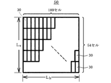
図5は、本発明に係る半導体演算装置の第1の実施形態における一つの演算器の一例の模式的平面図を示す。図5に示す一つの演算器50は、65nm技術世代の約10000ロジックセル(論理ゲート)で構成され、また、最近接の1タイムスロットで同時に通信可能な演算器数mを「36」とした場合の、9層(=m/4=36/4)積層される素子層のそれぞれに形成される複数の演算器の一つを示す。演算器50は、縦方向の寸法Lv、横方向の寸法Lhの方形領域内に配置される約10000個のロジックセル30から構成されている。すなわち、演算器50は、縦方向の寸法Lv内に54行分(=6行×9)配置されたロジックセルと、横方向の寸法Lh内に189列分(=21列×9)配置されたロジックセルの計10206個のロジックセルからなる。実寸では縦方向の寸法Lvは108μm(=20F×6行×9×0.1μm/F)、横方向の寸法Lhは94.5μm(=5F×21列×9×0.1μm/F)である。
演算器50は9層の素子層のそれぞれにおいて複数個、二次元アレイ状に配置され、そのうち、積層方向に相隣る2層の素子層に配置された演算器は、素子層表面上の縦方向に12(=Lv/(m/4)=108/9)μm、横方向に10.5(=Lh/(m/4)=94.5/9)μm相対的にずらして配置される。これは、図2に示した1つの演算器111又は112(いずれも図5の50に相当)の対角線14の方向にずらして配置されることに等しい。このように、演算器を配置、実装することによって各素子層の演算器の素子層貫通用配線領域(図4の31)を図6に示すように積層方向に重ねて配置することが可能となり、素子層貫通配線を積層方向に直線状に伸ばす効率的で最短の配線長の配線が可能となる。
図6は、ロジックセルによって構成される演算器の最適配置の一例の模式的平面図を示す。同図中、図2、図4と同一構成部分には同一符号を付してある。図6は、行方向のシフト量Lv/(m/4)をロジックセルの縦幅×2の場合として例示した2つの素子層の第1の演算器111と第2の演算器112の模式的平面図を示す。図6において、第1の演算器111は同じ行にロジックセル30、301、302等が配置されている。ロジックセル301、302は、それぞれ素子層貫通用配線領域311、312を有する。
本実施形態では、第1の演算器111を構成するすべてのロジックセル中の素子層貫通用配線領域が図6に401で模式的に示すように、同じ行のすべてのロジックセルの素子層貫通用配線領域の位置が一致して(すなわち、横方向に帯状に)配置されている。同様に、第2の演算器112を構成するすべてのロジックセル中の素子層貫通用配線領域が図6に402で模式的に示すように、同じ行のすべてのロジックセルの素子層貫通用配線領域の位置が一致して(すなわち、横方向に帯状に)配置されている。
更に、第1の演算器111の素子層貫通用配線領域401と、第2の演算器112の素子層貫通用配線領域402とは、図6に403で模式的に示すように積層方向に相隣る位置で重なって配置される。行方向のシフト量がロジックセルの縦幅で割り切れるように、演算器を実装することによって、素子層貫通用配線領域が403で模式的に示すように完全に重なるようになる。これにより、素子層間の通信路として用いる複数の素子層の間の層間配線を、複数の素子層を直線的に貫通する貫通配線とすることができ、効率的な配線ができる。
(第2の実施形態)
次に、本発明に係る半導体演算装置の第2の実施形態として、例えば深層学習における畳み込み演算に用いる例について説明する。
次に、本発明に係る半導体演算装置の第2の実施形態として、例えば深層学習における畳み込み演算に用いる例について説明する。
画像処理演算装置などにおける深層学習における畳み込み演算は、平面上に配置された画素について、例えば最近接のm画素(m=121=11×11、あるいはm=25=5×5)からデータを取り、それぞれのデータに適切な重み係数を乗算して積算する方法が公知の非特許文献(Alex Krizhevsky et al.,“ImageNet Classification with Deep Convolutional Neural Networks”,Proceedings of Neural Information Processing Systems(NIPS),pp.1-9,(2012))により知られている。
ここで、上記の画素数mを「36」(=6×6)とすると、上記の公知の深層学習における畳み込みの大きさは偶数となるが、5×5を包含する畳み込みが実現される。すなわち、本発明に係る半導体演算装置の演算器の配置方法を利用することにより、m/4(=36/4=9)層の素子層積層の実装によって1回ですべての素子層の演算器がデータの収集を終了することができる。
隣接する36個の演算器間でのデータ交換を例にとり、より正確に比較する。一平面上にすべての演算器が実装された場合、他の演算器と隣接する一辺を横切るデータは36演算器上にあるものを相互に通過させなければならない。したがって、すべての通信が終わるまでには、一つの演算器が送出すべきデータを相隣る演算器に対して送出する時間を1タイムスロットと定義すると36タイムスロットが必要となる。
これに対して、本発明に係る半導体演算装置の第2の実施形態では、同一平面上での通信を同一層内の相隣る4つの演算器とのみ交換するものとすると、残る32個の演算器に存在するデータを積層方向の32個の演算器間の層間通信により20倍の帯域幅を使って相互に通信することになる。したがって、1タイムスロットを上記の1.6倍(=32/20)に伸ばして相互の通信を行うことで、1タイムスロットで全通信を終了することとなる。結果として、本実施形態によれば、実時間で22.5倍(=1×36/(1.6×1))の高速化が達成されたことになる。すなわち、本実施形態では、図5に示したような構成の演算器が複数二次元アレイ状に配置された素子層を9(=m/4=36/4)層積層し、かつ、前述した層間配線を通信路とすることで、1タイムスロットで36(=m)個の最近接の演算器の間で同時に通信して畳み込み演算することができる。この傾向は中距離配線の配線幅が0.5μm程度の150nmプロセスでも同様となる。
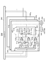
より具体的には、図7に示すような、畳み込み演算をパイプライン処理により実行する演算器を多並列に動作させる本発明に係る半導体演算装置を用いて、図8に例示するようなニューラルネットワークを計算する。図7は、本発明に係る半導体演算装置を用いたニューラルネットワークの畳み込み演算装置の一例の回路構成図を示す。同図において、畳み込み演算装置500は、入力セレクタ501、演算器502、ネットワーク503、及び出力セレクタ504から構成され、演算器502を構成するN個の演算器5021~502Nを多並列に動作させて畳み込み演算をパイプライン処理により実行する。なお、パイプライン処理を行う演算器5021~502Nのそれぞれは、例えば図5に示す一つの演算器50の構成である。
入力セレクタ501は入力データDをN分割して各分割データを演算器5021~502Nに別々に供給する。演算器5021~502Nはそれぞれ同一の回路構成で、入力セレクタ511、重み係数格納用キャッシュメモリ5121~5123、バッファメモリ5131~5133、セレクタ5141~5143、乗算器5151~5153、入力層データ格納用レジスタ516、加算器5171~5172、第1層計算用レジスタ5181、第2層計算用レジスタ5182、第1層計算結果格納用レジスタ5191~第L層計算結果格納用レジスタ519L、出力セレクタ520から構成されている。ネットワーク503はN個の演算器5021~502Nから出力されたデータをN個の演算器5021~502Nに選択入力する。更に出力セレクタ504はN個の演算器5021~502Nから出力されたデータを選択しM個の出力とする。
次に、畳み込み演算装置500の動作について詳細に説明する。以下、演算器5021~502Nのうち一つの演算器5021の動作について説明するが、他の(N-1)個の演算器5022~502Nも同様の動作を行う。まず、入力セレクタ501は入力データDをN分割し、N個の各分割データを演算器5021~502Nの各入力層データ格納用レジスタファイル516にそれぞれ格納する。
続いて、乗算器5151が、セレクタ5141を通して入力される入力層データ格納用レジスタファイル516からの入力分割データと、重み係数格納用キャッシュメモリ5121から読み出された第1層重み係数W(1)
ijとを乗算して加算器5171に供給する。加算器5171は第1層計算用レジスタ5181に蓄えられていた第1層のデータと乗算器5151からの乗算結果とを加算し、その加算結果を第1層計算用レジスタ5181に帰還入力する。また、乗算器5151は、他の演算器からネットワーク503を介して入力セレクタ511により選択されてバッファメモリ5131に保持されたデータも同様に、重み係数格納用キャッシュメモリ5121から読み出された第1層重み係数W(1)
ijと乗算し、その乗算結果を加算器5171において第1層計算用レジスタ5181からの第1層のデータと加算させる。
第1層重み係数W(1)
ijのすべてについて上記の乗算器5151による分割データ又は他の演算器からのデータとの乗算が行われ、それぞれの乗算結果の加算器5171の加算と第1層計算用レジスタ5181への格納が終了すると、入力層データ格納用レジスタファイル516が次の新たな分割データを格納すると共に、第1層計算用レジスタ5181の累積加算結果の格納データが第1層計算結果格納用レジスタ5191にコピーされる。入力層データ格納用レジスタファイル516に格納された次の新たな分割データに対しては、上記の最初に格納された分割データに対する処理と同様の処理が繰り返される。
一方、乗算器5152は、セレクタ5142を通して入力される第1層計算結果格納用レジスタ5191にコピーされた第1層の計算データと、重み係数格納用キャッシュメモリ5122から読み出された第2層重み係数W(2)
ijとを乗算して加算器5172に供給する。加算器5172は第2層計算用レジスタ5182に蓄えられていた第2層のデータと乗算器5152からの乗算結果とを加算し、その加算結果を第2層計算用レジスタ5182に帰還入力する。また、乗算器5152は、他の演算器からネットワーク503を介して入力セレクタ511により選択されてバッファメモリ5132に保持されたデータも同様に、重み係数格納用キャッシュメモリ5122から読み出された第2層重み係数W(2)
ijと乗算し、その乗算結果を加算器5172において第2層計算用レジスタ5182からの第2層のデータと加算する。
第2層重み係数W(1)
ijのすべてについて上記の乗算器5152による分割データ又は他の演算器からのデータとの乗算が行われ、それぞれの乗算結果の加算器5172の加算と第2層計算用レジスタ5182への格納が終了すると、入力層データ格納用レジスタファイル516が更に次の新たな分割データを格納すると共に、第2層計算用レジスタ5182の累積加算結果の格納データが第2層計算結果格納用レジスタ5192にコピーされる。以下同様に、各層において入力層データ格納用レジスタファイル516に格納される新たな分割データに対して、上記と同様の処理が繰り返される。上記の図7の演算装置500による畳み込み演算の上記の処理はニューラルネットワークのパイプライン処理により実行されており、これについて更に説明する。
図8は、図7に示した畳み込み演算装置におけるニューラルネットワークの計算処理について説明する図である。図8において、図7と同一構成部分には同一符号を付してある。図8において、図7のN個の演算器5021~502Nのそれぞれの演算処理を破線で囲んだ部分6021~602Nで模式的に示す。また、図8において、x1~xDはD個の入力データを示す。例えば、演算器5021においては、図8に破線で囲んだ部分6021内に模式的に示すように、入力データDをN分割して入力されて入力層データ格納用レジスタファイル516に格納された分割データx1、x2、x3、x4に対して、乗算器5151において第1層の重み係数W(1)
11、W(1)
21、W(1)
31、W(1)
41と乗算して、それらの乗算結果を加算器5171に供給する。また、乗算器5151はネットワーク503を介して他の演算器から入力されたデータx5と第1層の重み係数W(1)
51とを乗算して、その乗算結果を加算器5171に供給する。加算器5171は供給された上記の各乗算結果を加算して第1層の加算値y(1)
1を得て、それを第1層計算結果格納用レジスタ5191にコピーする。
続いて、第2層の乗算器5152は、第1層計算結果格納用レジスタ5191から入力された第1層の加算値y(1)と第2層の重み係数W(2)
11と乗算して得た乗算結果を得る。更に第2層の乗算器5152は、他の乗算器5152から入力された加算値y(1)
2と第2層の重み係数W(2)
21との乗算結果、及び他の乗算器5153から入力された加算値y(1)
3と第2層の重み係数W(2)
31との乗算結果をそれぞれ得る。加算器5172は第2層の乗算器5152により得られた上記の各乗算結果を加算して第2層の加算値y(2)
1を得る。ここで、第2層の乗算器5152では上記のように演算器5021~5023との間で通信を行って得た加算値y(1)
2、y(1)
3と自演算器に格納されている第2層の重み係数との乗算を行う。他の演算器5022~502Nにおいても乗算器5151と同様に他の演算器との通信を行って第1層の加算値を取得してその演算器内の第2層の重み係数との乗算を行う。以下、演算器5021~502Nのそれぞれにおいて第3層以上についても他の演算器との通信を行って上記と同様の処理を行う。
図8の例では、N個の演算器5021~502Nがm/4層の各素子層に分けて実装されているものとすると、各層のニューラルネットワークにおいて、m対1の通信がN組存在する。このように、演算器間でm対1の通信が必要となる場合には、平面上に実装されたN個の演算器からなる演算装置に対して、前述したように素子層がm層積層された本実施形態の演算装置によれば通信に必要なタイムスロットを1/mとすることができる。
10 半導体演算装置
111~113、50、502、5021~502N 演算器
12、121~12A 素子層
13、131~13A、201、202 層間配線
14 演算器の対角線
30、301、302 ロジックセル
31 素子層貫通用配線領域
33a 高電圧側電源用配線層
33b 低電圧側電源用配線層
34a、34b ゲート電極
35 第1の不純物拡散層
36 第2の不純物拡散層
37 出力配線層
38 素子層貫通配線
39 第2層配線層
40 第1層配線層
41 素子分離領域
42 ゲート絶縁膜
111 第1の演算器
112 第2の演算器
121 第1の素子層
122 第2の素子層
203 同一の素子層の演算器間を結ぶ配線
311、312、401、402 素子層貫通用配線領域
403 素子層111及び112の重なる位置にある素子層貫通用配線領域
500 畳み込み演算装置
501 入力セレクタ
503 ネットワーク
504 出力セレクタ
5121~5123 重み係数格納用キャッシュメモリ
5131~5133 バッファメモリ
5141~5143 セレクタ
5151~5153 乗算器
516 入力層データ格納用レジスタファイル
5171~5173 加算器
5181 第1層計算用レジスタ
5182 第2層計算用レジスタ
5191 第1層計算結果格納用レジスタ
5192 第2層計算結果格納用レジスタ
520 出力セレクタ
111~113、50、502、5021~502N 演算器
12、121~12A 素子層
13、131~13A、201、202 層間配線
14 演算器の対角線
30、301、302 ロジックセル
31 素子層貫通用配線領域
33a 高電圧側電源用配線層
33b 低電圧側電源用配線層
34a、34b ゲート電極
35 第1の不純物拡散層
36 第2の不純物拡散層
37 出力配線層
38 素子層貫通配線
39 第2層配線層
40 第1層配線層
41 素子分離領域
42 ゲート絶縁膜
111 第1の演算器
112 第2の演算器
121 第1の素子層
122 第2の素子層
203 同一の素子層の演算器間を結ぶ配線
311、312、401、402 素子層貫通用配線領域
403 素子層111及び112の重なる位置にある素子層貫通用配線領域
500 畳み込み演算装置
501 入力セレクタ
503 ネットワーク
504 出力セレクタ
5121~5123 重み係数格納用キャッシュメモリ
5131~5133 バッファメモリ
5141~5143 セレクタ
5151~5153 乗算器
516 入力層データ格納用レジスタファイル
5171~5173 加算器
5181 第1層計算用レジスタ
5182 第2層計算用レジスタ
5191 第1層計算結果格納用レジスタ
5192 第2層計算結果格納用レジスタ
520 出力セレクタ
Claims (7)
- 演算器が縦方向の寸法Lv、横方向の寸法Lhの方形領域内に配置され、かつ、2以上の前記演算器が同一層内で二次元アレイ状に配置された素子層が複数積層されており、
前記複数の素子層の積層方向に相隣る素子層において、それぞれ配置位置が重なる前記演算器同士が、互いに前記演算器の一つの対角線方向に相対的にずれて配置されるように前記複数の素子層を積層するとともに、前記相隣る素子層においてそれぞれ配置位置が重なる前記演算器同士を配線により接続し、層間の前記配線を通信路として用いることを特徴とする半導体演算装置。 - 前記複数の素子層は、少なくとも(m/4)層(ただし、mはメニーコアプロセッサにおいて、近接する演算器と1タイムスロットで同時通信可能な演算器の数)積層されており、積層方向に相隣る素子層それぞれに配置された前記演算器は、互いに素子層表面において縦方向にLv/(m/4)、横方向にLh/(m/4)の各寸法だけ相対的にずれて配置されていることを特徴とする請求項1記載の半導体演算装置。
- 前記複数の素子層のうち、それぞれ3以上の異なる素子層の配置位置が重なる各演算器の、配線領域位置が重なる配線領域同士を直線状に貫通して接続する貫通配線を有し、前記貫通配線を通信路として使用することを特徴とする請求項1又は2記載の半導体演算装置。
- 前記演算器を構成するロジックセルの中に、前記複数の素子層の中間配線層の配線ピッチのn倍(ただし、nは1以上の自然数)の幅の素子層貫通用配線領域が、前記横方向に帯状に形成されていることを特徴とする請求項1乃至3のうちいずれか一項記載の半導体演算装置。
- 前記素子層貫通用配線領域は、前記複数の素子層の互いに同じ位置に前記横方向に帯状に形成されていることを特徴とする請求項4記載の半導体演算装置。
- 前記素子層貫通用配線領域は、前記ロジックセルの電源用配線領域に隣接して平行に形成されていることを特徴とする請求項4又は5記載の半導体演算装置。
- 前記演算器は、各々縦方向の寸法が中間配線層の配線ピッチFのj倍、横方向の寸法が前記配線ピッチFのk倍の大きさのロジックセルが複数、前記縦方向の寸法Lv、横方向の寸法Lhの方形領域内に規則的に配置された構成であることを特徴とする請求項1乃至6のうちいずれか一項記載の半導体演算装置。
Priority Applications (1)
| Application Number | Priority Date | Filing Date | Title |
|---|---|---|---|
| JP2018520820A JP6839395B2 (ja) | 2016-05-30 | 2017-05-23 | 半導体演算装置 |
Applications Claiming Priority (2)
| Application Number | Priority Date | Filing Date | Title |
|---|---|---|---|
| JP2016-107757 | 2016-05-30 | ||
| JP2016107757 | 2016-05-30 |
Publications (1)
| Publication Number | Publication Date |
|---|---|
| WO2017208901A1 true WO2017208901A1 (ja) | 2017-12-07 |
Family
ID=60477777
Family Applications (1)
| Application Number | Title | Priority Date | Filing Date |
|---|---|---|---|
| PCT/JP2017/019176 Ceased WO2017208901A1 (ja) | 2016-05-30 | 2017-05-23 | 半導体演算装置 |
Country Status (2)
| Country | Link |
|---|---|
| JP (1) | JP6839395B2 (ja) |
| WO (1) | WO2017208901A1 (ja) |
Cited By (1)
| Publication number | Priority date | Publication date | Assignee | Title |
|---|---|---|---|---|
| CN109344541A (zh) * | 2018-10-31 | 2019-02-15 | 京微齐力(北京)科技有限公司 | 一种根据区域布线拥挤度判定布线方向的方法 |
Citations (2)
| Publication number | Priority date | Publication date | Assignee | Title |
|---|---|---|---|---|
| JP2008282108A (ja) * | 2007-05-08 | 2008-11-20 | Research Organization Of Information & Systems | 三次元集積電気回路の配線構造及びそのレイアウト方法 |
| JP2015176435A (ja) * | 2014-03-17 | 2015-10-05 | 国立研究開発法人産業技術総合研究所 | Lsiチップ積層システム |
Family Cites Families (3)
| Publication number | Priority date | Publication date | Assignee | Title |
|---|---|---|---|---|
| US8399973B2 (en) * | 2007-12-20 | 2013-03-19 | Mosaid Technologies Incorporated | Data storage and stackable configurations |
| US8258619B2 (en) * | 2009-11-12 | 2012-09-04 | International Business Machines Corporation | Integrated circuit die stacks with translationally compatible vias |
| US9087846B2 (en) * | 2013-03-13 | 2015-07-21 | Apple Inc. | Systems and methods for high-speed, low-profile memory packages and pinout designs |
-
2017
- 2017-05-23 JP JP2018520820A patent/JP6839395B2/ja active Active
- 2017-05-23 WO PCT/JP2017/019176 patent/WO2017208901A1/ja not_active Ceased
Patent Citations (2)
| Publication number | Priority date | Publication date | Assignee | Title |
|---|---|---|---|---|
| JP2008282108A (ja) * | 2007-05-08 | 2008-11-20 | Research Organization Of Information & Systems | 三次元集積電気回路の配線構造及びそのレイアウト方法 |
| JP2015176435A (ja) * | 2014-03-17 | 2015-10-05 | 国立研究開発法人産業技術総合研究所 | Lsiチップ積層システム |
Cited By (2)
| Publication number | Priority date | Publication date | Assignee | Title |
|---|---|---|---|---|
| CN109344541A (zh) * | 2018-10-31 | 2019-02-15 | 京微齐力(北京)科技有限公司 | 一种根据区域布线拥挤度判定布线方向的方法 |
| CN109344541B (zh) * | 2018-10-31 | 2023-01-31 | 京微齐力(北京)科技有限公司 | 一种根据区域布线拥挤度判定布线方向的方法 |
Also Published As
| Publication number | Publication date |
|---|---|
| JP6839395B2 (ja) | 2021-03-10 |
| JPWO2017208901A1 (ja) | 2019-03-28 |
Similar Documents
| Publication | Publication Date | Title |
|---|---|---|
| US11201148B2 (en) | Architecture for monolithic 3D integration of semiconductor devices | |
| US12292473B2 (en) | Yield improvements for three-dimensionally stacked neural network accelerators | |
| US11948060B2 (en) | Neural network accelerator tile architecture with three-dimensional stacking | |
| US20190057178A1 (en) | Integrated circuit layout wiring for multi-core chips | |
| TWI570586B (zh) | 用於包括奈米線及2d材料條之積體電路元件的設計工具 | |
| JP2012511263A (ja) | 3dマイクロアーキテクチャのシステムにおいて結合する平行プレーンメモリおよびプロセッサ | |
| US20210210601A1 (en) | Semiconductor device and method of producing the same | |
| TW202025444A (zh) | 在三維邏輯元件中對結合堆疊電晶體之邏輯單元進行垂直選路的方法 | |
| KR20220003516A (ko) | 복합 로직 셀들에 대한 컴팩트한 3d 적층 cfet 아키텍처 | |
| WO2020051144A1 (en) | Architecture design and processes for manufacturing monolithically integrated 3d cmos logic and memory | |
| Xu et al. | Optimal placement of vertical connections in 3D network-on-chip | |
| KR20200110608A (ko) | 개선된 컨택 및 슈퍼 비아를 포함하는 수직 전계 효과 트랜지스터 표준 셀 아키텍쳐 | |
| KR102753990B1 (ko) | Vfet 셀 및 vfet 셀을 포함하는 스캔 플립플롭 회로 | |
| JP7149647B2 (ja) | 半導体モジュール | |
| Kumar et al. | 3D multilayer mesh NoC communication and FPGA synthesis | |
| TWI859162B (zh) | 標準單元 | |
| Pentapati et al. | A logic-on-memory processor-system design with monolithic 3-D technology | |
| JP5305806B2 (ja) | 3次元集積回路の設計方法及び3次元集積回路の設計プログラム | |
| Musavvir et al. | Inter-tier process-variation-aware monolithic 3-D NoC design space exploration | |
| JPWO2017208901A1 (ja) | 半導体演算装置 | |
| CN113793844B (zh) | 一种三维集成芯片 | |
| US9639649B2 (en) | Semiconductor memory device, method for designing semiconductor memory device, and recording medium having designing method recorded therein | |
| JP2008282108A (ja) | 三次元集積電気回路の配線構造及びそのレイアウト方法 | |
| US12354660B2 (en) | Semiconductor devices | |
| Jabbar et al. | Impact of 3d ic on noc topologies: A wire delay consideration |
Legal Events
| Date | Code | Title | Description |
|---|---|---|---|
| ENP | Entry into the national phase |
Ref document number: 2018520820 Country of ref document: JP Kind code of ref document: A |
|
| NENP | Non-entry into the national phase |
Ref country code: DE |
|
| 121 | Ep: the epo has been informed by wipo that ep was designated in this application |
Ref document number: 17806458 Country of ref document: EP Kind code of ref document: A1 |
|
| 122 | Ep: pct application non-entry in european phase |
Ref document number: 17806458 Country of ref document: EP Kind code of ref document: A1 |