WO2017208693A1 - 人工光合成装置 - Google Patents
人工光合成装置 Download PDFInfo
- Publication number
- WO2017208693A1 WO2017208693A1 PCT/JP2017/016675 JP2017016675W WO2017208693A1 WO 2017208693 A1 WO2017208693 A1 WO 2017208693A1 JP 2017016675 W JP2017016675 W JP 2017016675W WO 2017208693 A1 WO2017208693 A1 WO 2017208693A1
- Authority
- WO
- WIPO (PCT)
- Prior art keywords
- semiconductor layer
- electrode
- semiconductor
- reduction electrode
- light
- Prior art date
- Legal status (The legal status is an assumption and is not a legal conclusion. Google has not performed a legal analysis and makes no representation as to the accuracy of the status listed.)
- Ceased
Links
Images



Classifications
-
- C—CHEMISTRY; METALLURGY
- C25—ELECTROLYTIC OR ELECTROPHORETIC PROCESSES; APPARATUS THEREFOR
- C25B—ELECTROLYTIC OR ELECTROPHORETIC PROCESSES FOR THE PRODUCTION OF COMPOUNDS OR NON-METALS; APPARATUS THEREFOR
- C25B1/00—Electrolytic production of inorganic compounds or non-metals
- C25B1/01—Products
- C25B1/02—Hydrogen or oxygen
- C25B1/04—Hydrogen or oxygen by electrolysis of water
-
- C—CHEMISTRY; METALLURGY
- C25—ELECTROLYTIC OR ELECTROPHORETIC PROCESSES; APPARATUS THEREFOR
- C25B—ELECTROLYTIC OR ELECTROPHORETIC PROCESSES FOR THE PRODUCTION OF COMPOUNDS OR NON-METALS; APPARATUS THEREFOR
- C25B11/00—Electrodes; Manufacture thereof not otherwise provided for
- C25B11/04—Electrodes; Manufacture thereof not otherwise provided for characterised by the material
- C25B11/042—Electrodes formed of a single material
-
- C—CHEMISTRY; METALLURGY
- C25—ELECTROLYTIC OR ELECTROPHORETIC PROCESSES; APPARATUS THEREFOR
- C25B—ELECTROLYTIC OR ELECTROPHORETIC PROCESSES FOR THE PRODUCTION OF COMPOUNDS OR NON-METALS; APPARATUS THEREFOR
- C25B3/00—Electrolytic production of organic compounds
- C25B3/20—Processes
- C25B3/25—Reduction
- C25B3/26—Reduction of carbon dioxide
-
- C—CHEMISTRY; METALLURGY
- C25—ELECTROLYTIC OR ELECTROPHORETIC PROCESSES; APPARATUS THEREFOR
- C25B—ELECTROLYTIC OR ELECTROPHORETIC PROCESSES FOR THE PRODUCTION OF COMPOUNDS OR NON-METALS; APPARATUS THEREFOR
- C25B9/00—Cells or assemblies of cells; Constructional parts of cells; Assemblies of constructional parts, e.g. electrode-diaphragm assemblies; Process-related cell features
-
- C—CHEMISTRY; METALLURGY
- C25—ELECTROLYTIC OR ELECTROPHORETIC PROCESSES; APPARATUS THEREFOR
- C25B—ELECTROLYTIC OR ELECTROPHORETIC PROCESSES FOR THE PRODUCTION OF COMPOUNDS OR NON-METALS; APPARATUS THEREFOR
- C25B9/00—Cells or assemblies of cells; Constructional parts of cells; Assemblies of constructional parts, e.g. electrode-diaphragm assemblies; Process-related cell features
- C25B9/17—Cells comprising dimensionally-stable non-movable electrodes; Assemblies of constructional parts thereof
- C25B9/19—Cells comprising dimensionally-stable non-movable electrodes; Assemblies of constructional parts thereof with diaphragms
-
- Y—GENERAL TAGGING OF NEW TECHNOLOGICAL DEVELOPMENTS; GENERAL TAGGING OF CROSS-SECTIONAL TECHNOLOGIES SPANNING OVER SEVERAL SECTIONS OF THE IPC; TECHNICAL SUBJECTS COVERED BY FORMER USPC CROSS-REFERENCE ART COLLECTIONS [XRACs] AND DIGESTS
- Y02—TECHNOLOGIES OR APPLICATIONS FOR MITIGATION OR ADAPTATION AGAINST CLIMATE CHANGE
- Y02E—REDUCTION OF GREENHOUSE GAS [GHG] EMISSIONS, RELATED TO ENERGY GENERATION, TRANSMISSION OR DISTRIBUTION
- Y02E60/00—Enabling technologies; Technologies with a potential or indirect contribution to GHG emissions mitigation
- Y02E60/30—Hydrogen technology
- Y02E60/36—Hydrogen production from non-carbon containing sources, e.g. by water electrolysis
Definitions
- the present disclosure relates to an artificial photosynthesis device capable of artificially performing photosynthesis.
- an artificial photosynthesis system that artificially performs photosynthesis that generates oxygen together with a carbon compound (such as methanol) containing hydrogen or carbon from water and carbon dioxide using light energy of sunlight has been studied.
- a carbon compound such as methanol
- Patent Document 1 discloses that carbon dioxide is reduced to formic acid using a metal complex that exhibits a reducing action of a semiconductor and carbon dioxide.
- Patent Document 2 discloses that a carbon compound or hydrogen is generated using a SiC / Si based semiconductor.
- Non-Patent Document 1 discloses generating hydrogen using a GaAs-based semiconductor.
- This disclosure is intended to provide an artificial photosynthesis device capable of improving the generation efficiency of reaction products.
- the artificial photosynthesis device includes a condenser lens and a semiconductor photocatalyst.
- the condensing lens condenses light at a predetermined magnification.
- the semiconductor photocatalyst includes a semiconductor layer that absorbs the light collected by the condenser lens and generates an internal photoelectric effect, a reduction electrode that reduces carbon dioxide to generate a carbon compound, and oxygen and hydrogen by oxidizing water. And an oxidation electrode for generating ions.
- the semiconductor layer, the reduction electrode, and the oxidation electrode are integrated.
- the semiconductor layer absorbs light and emits heat, and the heat generated in the semiconductor layer is transmitted to the reduction electrode and the oxidation electrode.
- a semiconductor photocatalyst in which a semiconductor layer, a reduction electrode, and an oxidation electrode are integrated is condensed by a condenser lens, so that the electrode is heated with heat energy generated in the semiconductor layer by light absorption. Temperature can be increased, and the reaction rate of the electrode reaction can be increased. As a result, the thermal energy generated in the semiconductor layer can be actively used for the electrode reaction on the electrode surface.
- the artificial photosynthesis apparatus 1 according to the first embodiment of the present disclosure will be described.
- the artificial photosynthesis apparatus 1 of the present embodiment is used to perform oxygen generation, hydrogen generation, and carbon compound (methanol etc.) generation by irradiating sunlight.
- the artificial photosynthesis device 1 includes a container 10.
- the container 10 contains an electrolyte solution 11.
- the electrolytic solution 11 is not particularly limited, but in this embodiment, an aqueous potassium hydrogen carbonate solution is used.
- concentration of the aqueous potassium hydrogen carbonate solution is 0.1 mol / L.
- the container 10 is provided with a semiconductor photocatalyst 12.
- the semiconductor photocatalyst 12 is immersed in the electrolytic solution 11.
- the semiconductor photocatalyst 12 has the same configuration as that of a solar cell, and includes a semiconductor layer 12a, a reduction electrode 12b, and an oxidation electrode 12c.
- the reduction electrode 12b is formed on the surface on the one surface side of the semiconductor layer 12a, and the reduction electrode 12b is formed on the surface on the other surface side of the semiconductor layer 12a.
- a reduction electrode 12b is formed on the upper side of the semiconductor layer 12a, and an oxidation electrode 12c is formed on the lower side of the semiconductor layer 12a. That is, the semiconductor photocatalyst 12 is configured by integrating the semiconductor layer 12a, the reduction electrode 12b, and the oxidation electrode 12c.
- the semiconductor photocatalyst 12 when sunlight is irradiated, electron / hole pairs are generated by the internal photoelectric effect (photovoltaic effect).
- the semiconductor layer 12a absorbs sunlight and generates an internal photoelectric effect.
- electrons move to the reduction electrode 12b, holes move to the oxidation electrode 12c, and a potential difference is generated between the electrodes 12b and 12c.
- a III-V semiconductor that is a direct transition semiconductor is used as the semiconductor layer 12a.
- the group III-V semiconductor of this embodiment has a tandem structure of two junctions or three junctions and is a tunnel junction.
- III-V semiconductors include GaInP / GaAs / Ge, GaInP / GaAs / GaNAs, GaInP / GaAs, AlGaInP / GaAs / Ge, AlGaInP / GaAs / GaNAs, and AlGaInP / GaAs.
- a PN junction is formed, and the substrate is a Ge substrate or a GaAs substrate. Two PN junctions are two junctions and three PN junctions are three junctions.
- a Si semiconductor may be used as the substrate of the III-V group semiconductor.
- the reduction electrode 12b is formed on the surface of the semiconductor layer 12a.
- a transparent electrode such as ITO or FTO
- the reduction electrode 12b can be formed.
- the following reduction reaction of carbon dioxide is performed, and a carbon compound (such as methanol) and hydrogen are generated.
- the oxidation electrode 12c is formed on the surface of the semiconductor layer 12a opposite to the reduction electrode 12b.
- An oxidation electrode 12c can be formed by forming an IrO 2 electrode or a RuO 2 electrode on the surface of the semiconductor layer 12a. On the surface of the oxidation electrode 12c, the following water oxidation reaction is performed, and hydrogen ions and oxygen are generated.
- the container 10 is provided with an electrolyte membrane 13.
- the electrolyte membrane 13 is disposed between the reduction electrode 12b and the oxidation electrode 12c.
- the electrolyte membrane 13 separates the electrolyte solution 11 on the reduction electrode 12b side and the oxidation electrode 12c side while allowing movement of hydrogen ions.
- Nafion registered trademark of DuPont
- DuPont can be used as the electrolyte membrane 13.
- a condenser lens 14 is provided outside the container 10.
- the condensing lens 14 has a function of concentrating sunlight on the reduction electrode 12b.
- the condenser lens 14 for example, a spherical lens or a Fresnel lens can be used.
- the semiconductor layer 12 a absorbs sunlight collected by the condenser lens 14. By condensing sunlight with the condensing lens 14, the conversion efficiency from the light energy to the electrical energy in the semiconductor layer 12a can be improved.
- the group III-V semiconductor used as the semiconductor layer 12a in this embodiment has a great effect of improving the conversion efficiency by light collection.
- the magnification of the condenser lens 14 is 5 to 1000 times.
- the magnification of the condenser lens 14 can be adjusted by the refractive index of the condenser lens 14 or the like.
- the semiconductor layer 12a generates heat by absorbing sunlight.
- the temperature of the semiconductor layer 12a can be controlled. Specifically, when the magnification of the condenser lens 14 is increased, the temperature of the semiconductor layer 12a is increased, and when the magnification of the condenser lens 14 is decreased, the temperature of the semiconductor layer 12a is decreased.
- a CO 2 supply pipe 15 is inserted into the container 10. Carbon dioxide is supplied from the CO 2 supply pipe 15 to the reduction electrode 12 b side in the electrolyte solution 11.
- FIG. 2 shows the potential measured with reference to the standard hydrogen electrode, the oxidation potential of water, the reduction potential of carbon dioxide, and the energy band diagram of the semiconductor layer 12a.
- a two-junction composed of a GaInP layer and a GaAs layer is employed as the semiconductor layer 12a.
- the GaInP layer and the GaAs layer are heterojunction. Sunlight enters from the GaInP layer side of the semiconductor layer 12a.
- the lower end potential of the conduction band on the GaInP side is more negative than the reduction potential of carbon dioxide
- the upper end potential of the valence band on the GaAs side is more positive than the oxidation potentials of oxygen and water. I have to.
- the lower end potential of the conduction band on the GaInP layer side and the upper end potential of the valence band on the GaAs layer side are set by adjusting the conductivity type and impurity concentration of the GaAs layer and GaInP layer.
- the energy level difference between the conduction band of the GaAs layer and the valence band of the GaInP layer is small.
- the vicinity of the heterojunction in the GaAs side N-type region and the vicinity of the heterojunction in the GaInP side P-type region are made to be highly doped semiconductors.
- the tunneling phenomenon is caused by reducing the energy level difference between the lower end of the conduction band of the GaAs layer and the upper end of the valence band of the GaInP layer and making the transition region of the heterojunction thin and high in concentration. A tunnel current flows.
- the band is bent by the PN junction so that the electrons of the electron / hole pair generated in the GaAs layer move to the heterojunction side, and the holes move to the surface side opposite to the heterojunction. That is, the band on the conduction band side of the GaAs layer is bent so as to incline downward toward the heterojunction side, and the band on the valence band side is also bent so as to incline downward toward the heterojunction side. It is done.
- the band is bent by the PN junction so that the electrons of the electron / hole pair generated in the GaInP layer move to the back side opposite to the heterojunction, and the holes move to the heterojunction side. That is, the band on the conduction band side of the GaInP layer is bent so as to incline upward toward the heterojunction side, and the band on the valence band side is also bent so as to incline upward toward the heterojunction side.
- the semiconductor layer 12a As shown in FIG. 2, in the GaInP layer and the GaAs layer constituting the semiconductor layer 12a, electrons are excited by the internal photoelectric effect when irradiated with sunlight, but a part of the incident light energy is released as heat. Is done. For this reason, the semiconductor layer 12a generates heat when irradiated with sunlight.
- the semiconductor layer 12a, the reduction electrode 12b, and the oxidation electrode 12c are integrated, the heat generated in the semiconductor layer 12a is directly transmitted to the reduction electrode 12b and the oxidation electrode 12c. Thereby, the temperature of the semiconductor layer 12a, the reduction electrode 12b, and the oxidation electrode 12c rises.
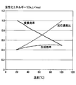
- FIG. 3 and 4 show the conversion efficiency of the semiconductor layer 12a from sunlight to electricity and the reaction rate ratio of the electrode reaction on the surfaces of the electrodes 12b and 12c.
- the conversion efficiency from sunlight to electricity at 20 ° C. is 1, and the reaction rate ratio at 100 ° C. is 1.
- FIG. 3 shows a case where the activation energy is 10 kJ / mol
- FIG. 4 shows a case where the activation energy is 30 kJ / mol.
- the activation energy is energy necessary for the electrode reaction described above to proceed at the reduction electrode 12b and the oxidation electrode 12c.
- the conversion efficiency from sunlight to electricity of the semiconductor layer 12a decreases as the temperature rises.
- the reaction rate of the electrode reaction increases with increasing temperature.
- the production efficiency of the reaction product in the electrode reaction is obtained by multiplying the conversion efficiency of the semiconductor layer 12a from sunlight into electricity and the reaction rate ratio of the electrode reaction. As shown in FIG. 3, when the activation energy is 10 kJ / mol, the generation efficiency of the reaction product is maximized around 80 ° C. As shown in FIG. 4, when the activation energy is 30 kJ / mol, the production efficiency of the reaction product is maximized around 100 ° C. At a temperature exceeding 100 ° C., the temperature of the semiconductor photocatalyst 12 is desirably 100 ° C. or less because the electrodes 12b and 12c are deteriorated and the electrolytic solution 11 is boiled.
- the temperature of the semiconductor photocatalyst 12 is controlled aiming at a temperature at which the generation efficiency of the reaction product is maximized.
- the temperature of the semiconductor layer 12a can be controlled by adjusting the condensing by the condensing lens 14. Specifically, by adjusting the magnification, focus, position, or direction of the condensing lens 14, the condensing by the condensing lens 14 can be adjusted, and the temperature of the semiconductor layer 12a can be controlled.
- the magnification of the condenser lens 14 may be set in advance so that the semiconductor layer 12a has a desired temperature.
- the artificial photosynthesis apparatus 1 according to this embodiment is configured as described above. Next, operation
- the semiconductor photocatalyst 12 is used in a state where it is immersed in the electrolytic solution 11 accommodated in the case 10 of the artificial photosynthesis apparatus 1, and artificial photosynthesis is performed by irradiating sunlight from the reduction electrode 12b side. Done.
- the electron / hole pair When light energy is absorbed by the semiconductor layer 12a by the irradiation of sunlight, the electron / hole pair is excited by the absorbed light on the GaAs layer side, and the bending of the band causes the electrons to be on the heterojunction side and the holes to be the oxidation electrode 12c. Move to the side (opposite the heterojunction). Similarly, on the GaInP layer side, the electron / hole pair is excited by the absorbed light, and the holes move to the heterojunction side and the electrons move to the reduction electrode 12b side (the opposite side of the heterojunction).
- holes having energy capable of oxidizing water gather at the oxidation electrode 12c, and water is oxidized, that is, oxygen and hydrogen ions are generated.
- hydrogen ions generated on the oxidation electrode 12c side are reduced to generate hydrogen.
- carbon dioxide is flowed, carbon dioxide is reduced at the reduction electrode 12c, and a carbon compound (methanol or the like) is synthesized. By repeating such a reaction, oxygen generation and carbon compound generation are continuously performed.
- sunlight is collected by the condenser lens 14 with respect to the semiconductor photocatalyst 12 in which the semiconductor layer 12a, the reduction electrode 12b, and the oxidation electrode 12c are integrated.
- the thermal energy generated in the semiconductor layer 12a can be actively used for the electrode reaction on the surfaces of the electrodes 12b and 12c.
- the temperature of the semiconductor photocatalyst 12 is controlled by optimizing the condenser lens 14 so that the generation efficiency of the reaction product is maximized.
- the semiconductor layer 12a balances the decrease in the conversion efficiency of the semiconductor layer 12a from sunlight into electricity accompanying the temperature rise and the increase in the reaction rate of the electrode reaction accompanying the temperature rise. It is possible to make the most effective use of the generated heat energy.
- the reduction electrode 12b is provided so as to extend from one surface side (the upper side in FIG. 5) of the semiconductor layer 12a.
- the reduction electrode 12b has a substantially conical surface shape or a slope shape, and the diameter increases as the distance from the semiconductor layer 12a increases.
- a metal electrode such as Cu, In, Sn, or a conductive material having conductivity can be used as the reduction electrode 12b.
- Pt, NiCo 3 O 4 or the like may be provided as a catalyst electrode on the surface of the reduction electrode 12b.
- the electrolytic solution 11 exists below the reduction electrode 12b, but does not exist above the reduction electrode 12b. For this reason, the one surface side provided with the reduction electrode 12b in the semiconductor layer 12a is exposed to the atmosphere. Therefore, sunlight is directly applied to the surface on the one surface side of the semiconductor layer 12a.
- the heat energy generated in the semiconductor layer 12a by condensing sunlight by the condenser lens 14 is transferred to the surfaces of the electrodes 12b and 12c. It can be used effectively for electrode reactions.
- the electrode reaction proceeds on the surface of the cathode catalyst 12b extended from the semiconductor layer 12a. For this reason, the electrode reaction does not proceed on the surface on the one surface side (upper side in FIG. 5) of the semiconductor layer 12a on which the cathode catalyst 12b is provided, and the deterioration of the one surface surface of the semiconductor layer 12a can be suppressed.
- sunlight is directly incident on one surface side of the semiconductor layer 12a exposed to the atmosphere. Thereby, the conversion efficiency from sunlight to electricity in the semiconductor layer 12a can be improved.
- a lens adjustment mechanism capable of changing the magnification, focus, position, or direction of the condenser lens 14 may be provided. By adjusting at least one of the magnification, focal point, position, and direction of the condenser lens 14 with such a lens adjustment mechanism, it is possible to adjust the temperature when the semiconductor photocatalyst 12 absorbs sunlight.
- a temperature sensor that detects the temperature of the semiconductor photocatalyst 12 and a control device that controls the lens adjustment mechanism based on the temperature of the semiconductor photocatalyst 12 detected by the temperature sensor may be provided.
- the condensing lens 14 can be adjusted based on the temperature of the semiconductor photocatalyst 12, and the temperature of the semiconductor photocatalyst 12 can be controlled more appropriately.
- a mediator may be included on the reducing electrode 12b side of the electrolytic solution 11.
- a mediator is a compound that mediates electron transfer through a carbon dioxide reduction reaction.
- a nitrogen-containing aromatic compound can be used as the mediator.
- the aromatic compound is a planar ring having a delocalized ⁇ electron system containing 4n + 2 (n is an integer) ⁇ electrons.
- Aromatic rings can be formed by 5, 6, 7, 8, 9, or 10 or more atoms.
- Aromatic compounds include monocyclic and fused ring polycyclic.
- the nitrogen-containing aromatic compound is a heteroaromatic compound in which one or more constituent atoms of the aromatic ring are N atoms.
- one or more hydrogen atoms bonded to the constituent atoms of the aromatic ring may be substituted with a linear or branched lower alkyl group, a hydroxy group, an amino group, or a pyridyl group.
- nitrogen-containing aromatic compounds constituting such mediators include imidazole, methylimidazole, dimethylimidazole, triazole, pyridine, and dimethylaminopyridine.
Landscapes
- Chemical & Material Sciences (AREA)
- Organic Chemistry (AREA)
- Engineering & Computer Science (AREA)
- Chemical Kinetics & Catalysis (AREA)
- Electrochemistry (AREA)
- Materials Engineering (AREA)
- Metallurgy (AREA)
- Inorganic Chemistry (AREA)
- Electrolytic Production Of Non-Metals, Compounds, Apparatuses Therefor (AREA)
- Electrodes For Compound Or Non-Metal Manufacture (AREA)
- Catalysts (AREA)
Abstract
人工光合成装置は、集光レンズ(14)と、半導体光触媒(12)と、を備える。集光レンズは、光を所定の倍率で集光する。半導体光触媒は、集光レンズによって集光された光を吸収して内部光電効果を発生させる半導体層(12a)と、二酸化炭素を還元して炭素化合物を生成する還元電極(12b)と、水を酸化して酸素および水素イオンを生成する酸化電極(12c)と、を有する。半導体触媒において、半導体層、還元電極および酸化電極は一体化されている。半導体層は光を吸収して熱を発し、半導体層で発生した熱は還元電極および酸化電極に伝えられる。
Description
本出願は、2016年6月2日に出願された日本出願番号2016-110987号に基づくもので、ここにその記載内容を援用する。
本開示は、人工的に光合成を行うことが可能な人工光合成装置に関するものである。
従来より、太陽光の光エネルギーを利用して、水と二酸化炭素から水素や炭素を含む炭素化合物(メタノールなど)と共に酸素を生成する光合成を人工的に行う人工光合成システムが研究されている。
例えば、特許文献1では、半導体と二酸化炭素の還元作用を呈する金属錯体を用いて、二酸化炭素をギ酸に還元することが開示されている。特許文献2には、SiC/Si系半導体を用いて炭素化合物や水素を生成することが開示されている。非特許文献1には、GaAs系半導体を用いて水素を生成することが開示されている。
Turner et al., Science 17 April 1998 vol.280, Issue 5362, pp.425-427
しかしながら、上述した従来技術の人工光合成では、水素や炭素化合物といった反応生成物の生成効率が低いという課題がある。
本開示は、反応生成物の生成効率を向上させることが可能な人工光合成装置を提供することを目的とする。
本開示の一態様によれば、人工光合成装置は、集光レンズと、半導体光触媒と、を備える。集光レンズは、光を所定の倍率で集光する。半導体光触媒は、集光レンズによって集光された光を吸収して内部光電効果を発生させる半導体層と、二酸化炭素を還元して炭素化合物を生成する還元電極と、水を酸化して酸素および水素イオンを生成する酸化電極と、を有する。
半導体触媒において、半導体層、還元電極および酸化電極は一体化されている。半導体層は光を吸収して熱を発し、半導体層で発生した熱は還元電極および酸化電極に伝えられる。
本開示の一態様によれば、半導体層、還元電極および酸化電極が一体化された半導体光触媒に対し、集光レンズによって集光することで、光の吸収によって半導体層で発生する熱エネルギーで電極を温度上昇させることができ、電極反応の反応速度を上げることができる。この結果、半導体層で発生する熱エネルギーを電極表面での電極反応に積極的に有効利用できる。
本開示についての上記目的およびその他の目的、特徴や利点は、添付の図面を参照しながら下記の詳細な記述により、より明確になる。図面において、
第1実施形態の人工光合成装置の全体構成を示す説明図であり、
半導体層のエネルギーバンドを示す説明図であり、
温度変化した場合の半導体光触媒の変換効率、電極反応の反応速度、反応生成物の生成効率を示すグラフであり、
温度変化した場合の半導体光触媒の変換効率、電極反応の反応速度、反応生成物の生成効率を示すグラフであり、
第2実施形態の人工光合成装置の全体構成を示す説明図である。
以下、本開示の実施形態について図に基づいて説明する。なお、以下の各実施形態相互において、互いに同一もしくは均等である部分には、同一符号を付して説明を行う。
(第1実施形態)
本開示の第1実施形態にかかる人工光合成装置1について説明する。本実施形態の人工光合成装置1は、太陽光を照射することで酸素生成、水素生成および炭素化合物(メタノール等)生成を行うものとして用いられる。
本開示の第1実施形態にかかる人工光合成装置1について説明する。本実施形態の人工光合成装置1は、太陽光を照射することで酸素生成、水素生成および炭素化合物(メタノール等)生成を行うものとして用いられる。
図1に示すように、人工光合成装置1は、容器10を備えている。容器10には、電解液11が収容されている。電解液11は特に限定されないが、本実施形態では炭酸水素カリウム水溶液を用いている。炭酸水素カリウム水溶液の濃度は、0.1mol/Lとしている。
容器10には、半導体光触媒12が設けられている。半導体光触媒12は、電解液11に浸された状態となっている。半導体光触媒12は、太陽電池と同様の構成であり、半導体層12a、還元電極12b、酸化電極12cを備えている。
半導体層12aの一面側の表面上に還元電極12bが形成され、半導体層12aの他面側の表面上に還元電極12bが形成されている。図1では、半導体層12aの上側に還元電極12bが形成され、半導体層12aの下側に酸化電極12cが形成されている。つまり、半導体光触媒12は、半導体層12a、還元電極12bおよび酸化電極12cが一体化して構成されている。
半導体光触媒12では、太陽光が照射されると内部光電効果(光起電力効果)によって電子/正孔対が発生する。換言すると、半導体層12aは、太陽光を吸収して内部光電効果を発生させる。この結果、電子が還元電極12bに移動し、正孔が酸化電極12cに移動し、電極間12b、12cに電位差が発生する。
本実施形態では、半導体層12aとして直接遷移型半導体であるIII-V族半導体を用いている。本実施形態のIII-V族半導体は、2接合または3接合のタンデム構造であり、トンネル接合となっている。そのようなIII-V族半導体としては、GaInP/GaAs/Ge、GaInP/GaAs/GaNAs、GaInP/GaAs、AlGaInP/GaAs/Ge、AlGaInP/GaAs/GaNAs、AlGaInP/GaAsを例示でき、各半導体は各々PN接合を形成し、基板はGe基板若しくはGaAs基板を用いる。このPN接合が2つのときが2接合で、3つのときが3接合である。また、III-V族半導体の基板としてSi半導体を用いてもよい。
還元電極12bは、半導体層12aの表面上に形成されている。半導体層12aの表面にITOやFTO等の透明電極を成膜することで、還元電極12bを形成することができる。還元電極12bの表面では、以下に示す二酸化炭素の還元反応が行われ、炭素化合物(メタノール等)および水素が生成する。
CO2+6H++6e-→CH3OH+H2O
2H++2e-→H2
酸化電極12cは、半導体層12aにおける還元電極12bとは反対側の表面上に形成されている。半導体層12aの表面にIrO2電極若しくはRuO2電極等を成膜することで、酸化電極12cを形成することができる。酸化電極12cの表面では、以下に示す水の酸化反応が行われ、水素イオンおよび酸素が生成する。
2H++2e-→H2
酸化電極12cは、半導体層12aにおける還元電極12bとは反対側の表面上に形成されている。半導体層12aの表面にIrO2電極若しくはRuO2電極等を成膜することで、酸化電極12cを形成することができる。酸化電極12cの表面では、以下に示す水の酸化反応が行われ、水素イオンおよび酸素が生成する。
2H2O+4h+→4H++O2
酸化電極12c側で発生した水素イオンは、還元電極12b側に移動し、上述した二酸化炭素の還元反応に用いられる。
酸化電極12c側で発生した水素イオンは、還元電極12b側に移動し、上述した二酸化炭素の還元反応に用いられる。
容器10には、電解質膜13が設けられている。電解質膜13は、還元電極12bと酸化電極12cの間に配置される。電解質膜13は、水素イオンの移動を許容しつつ、還元電極12b側と酸化電極12c側で電解液11を分離する。電解質膜13としては、例えばナフィオン(デュポン社の登録商標)を用いることができる。
容器10の外部には、集光レンズ14が設けられている。集光レンズ14は、太陽光を還元電極12bに集光する機能を備えている。集光レンズ14としては、例えば球面レンズまたはフレネルレンズを用いることができる。
半導体層12aは、集光レンズ14によって集光された太陽光を吸収する。集光レンズ14によって太陽光を集光することで、半導体層12aにおける光エネルギーから電気エネルギーへの変換効率を向上させることができる。特に、本実施形態で半導体層12aとして用いているIII-V族半導体は、集光による変換効率を向上させる効果が大きい。
本実施形態では、集光レンズ14の倍率を5~1000倍としている。集光レンズ14の倍率は、集光レンズ14の屈折率等によって調整することができる。後述するように、半導体層12aは太陽光を吸収することで発熱する。集光レンズ14の倍率を変化させることで、半導体層12aの温度を制御することができる。具体的には、集光レンズ14の倍率を高くすると半導体層12aの温度が高くなり、集光レンズ14の倍率を低くすると半導体層12aの温度が低くなる。
容器10には、CO2供給管15が挿入されている。CO2供給管15から二酸化炭素が電解液11における還元電極12b側に供給される。
図2は、標準水素電極を基準にして測定した電位と水の酸化電位および二酸化炭素の還元電位と、半導体層12aのエネルギーバンド図を示している。図2に示すように、本実施形態では、半導体層12aとしてGaInP層およびGaAs層からなる2接合を採用している。GaInP層およびGaAs層はヘテロ接合されている。太陽光は、半導体層12aのGaInP層側から入射する。
図2に示すように、GaInP側の伝導帯の下端電位が二酸化炭素の還元電位よりもマイナス側となり、GaAs側の価電子帯の上端電位が酸素および水の酸化電位よりもプラス側となるようにしている。具体的には、GaAs層やGaInP層の導電型や不純物濃度の調整によって、GaInP層側の伝導帯の下端電位やGaAs層側の価電子帯の上端電位を設定している。
さらに、GaAs側で励起される電子/正孔とGaInP側で励起される電子/正孔を連続的につなぐために、GaAs層の伝導帯とGaInP層の価電子帯のエネルギー準位差が小さくなるようにし、且つGaAs側N型領域のヘテロ接合近傍部とGaInP側のP型領域のヘテロ接合近傍部が高濃度ドーピングの半導体となるようにしている。このように、GaAs層の伝導帯の下端とGaInP層の価電子帯の上端のエネルギー準位差を小さくし、かつ、ヘテロ接合の遷移領域を薄く高濃度にすることで、トンネル現象が生じてトンネル電流が流れるようになる。
また、GaAs層で生成した電子/正孔対の電子がヘテロ接合側へ移動し、正孔がヘテロ接合の反対側となる表面側へ移動するようにPN接合によってバンドが曲げられる。つまり、GaAs層の伝導帯側のバンドは、ヘテロ接合側に向かって下側に傾斜するように曲げられ、価電子帯側のバンドも、ヘテロ接合側に向かって下側に傾斜するように曲げられる。
同様に、GaInP層で生成した電子/正孔対の電子がヘテロ接合と反対側となる裏側へ移動し、正孔がヘテロ接合側へ移動するようにPN接合によってバンドが曲げられる。つまり、GaInP層の伝導帯側のバンドは、ヘテロ接合側に向かって上側に傾斜するように曲げられ、価電子帯側のバンドも、ヘテロ接合側に向かって上側に傾斜するように曲げられる。
このようにすることで、伝導帯側では電子がよりGaInP層における表面側に移動し易くなると共に、価電子帯側では正孔がよりGaAs層の表面側に移動し易くなって、電子と正孔を遠ざけられる。したがって、キャリアを分離することができて再結合を抑制することが可能となる。また、GaAs側の電子とGaInP側の正孔がヘテロ接合に集まり再結合によるトンネルが起き易くなる。
図2に示すように、半導体層12aを構成するGaInP層およびGaAs層では、太陽光が照射されることで内部光電効果によって電子が励起されるが、入射光エネルギーのうち一部は熱として放出される。このため、太陽光が照射されることで半導体層12aは発熱する。
本実施形態では、半導体層12a、還元電極12bおよび酸化電極12cが一体化されているので、半導体層12aで発生した熱は、還元電極12bおよび酸化電極12cに直接伝えられる。これにより、半導体層12a、還元電極12bおよび酸化電極12cが温度上昇する。
図3および図4は、半導体層12aの太陽光から電気への変換効率、電極12b、12c表面における電極反応の反応速度比を示している。図3および図4では、20℃での太陽光から電気への変換効率を1とし、100℃での反応速度比を1としている。図3は、活性化エネルギーが10kJ/molの場合を示し、図4は、活性化エネルギーが30kJ/molの場合を示している。活性化エネルギーは、還元電極12bと酸化電極12cで上述した電極反応が進行するために必要なエネルギーである。
図3、図4に示すように、半導体層12aの太陽光から電気への変換効率は温度上昇に伴って低下する。一方、電極反応の反応速度は温度上昇に伴って上昇する。
電極反応における反応生成物の生成効率は、半導体層12aの太陽光から電気への変換効率と、電極反応の反応速度比を乗じることで得られる。図3に示すように、活性化エネルギーが10kJ/molの場合は、80℃付近で反応生成物の生成効率が最大となっている。図4に示すように、活性化エネルギーが30kJ/molの場合は、100℃付近で反応生成物の生成効率が最大となっている。100℃を超える温度では、電極12b、12cの劣化が進行すること、電解液11が沸騰すること等の理由から、半導体光触媒12の温度は100℃以下とすることが望ましい。
本実施形態では、反応生成物の生成効率が最大となる温度を狙って半導体光触媒12を温度制御している。これにより、太陽光の集光によって半導体光触媒12で発生する熱エネルギーを、電極12b、12c表面で進行する電極反応に積極的に利用することができる。
集光レンズ14による集光を調整することで、半導体層12aの温度を制御することができる。具体的には、集光レンズ14の倍率、焦点、位置あるいは方向等を調整することで、集光レンズ14による集光を調整することができ、半導体層12aの温度が制御可能となる。例えば、半導体層12aが所望の温度となるように、予め集光レンズ14の倍率を設定すればよい。
以上のような構成により、本実施形態の人工光合成装置1が構成されている。次に、本実施形態の人工光合成装置1の動作について説明する。
上記したように、半導体光触媒12は、人工光合成装置1におけるケース10に収容した電解液11の中に浸された状態で使用され、還元電極12b側から太陽光が照射されることで人工光合成が行われる。
太陽光の照射によって半導体層12aに光エネルギーが吸収されると、GaAs層側では吸収した光で電子/正孔対が励起され、バンドの曲がりにより電子はヘテロ接合側、正孔は酸化電極12c側(ヘテロ接合の反対側)へ移動する。同様に、GaInP層側では吸収した光で電子/正孔対が励起され、バンドの曲がりにより正孔はヘテロ接合側、電子は還元電極12b側(ヘテロ接合の反対側)へ移動する。
そして、GaAs層側のヘテロ接合に集まる電子とGaInP層側のヘテロ接合に集まる正孔がトンネル現象によって再結合し、GaAs層側とGaInP層側との2段励起が連続的に繋がることになる。
また、酸化電極12cでは水を酸化可能なエネルギーを持った正孔が集まり、水の酸化、すなわち酸素生成と水素イオン生成が行われる。還元電極12bでは、酸化電極12c側で生成した水素イオンを還元して水素が生成される。二酸化炭素を流した場合には、還元電極12cで二酸化炭素が還元され、炭素化合物(メタノール等)が合成される。このような反応が繰り返されることで、酸素生成および炭素化合物生成が連続的に行われる。
以上説明した本実施形態では、半導体層12a、還元電極12bおよび酸化電極12cが一体化された半導体光触媒12に対して、集光レンズ14によって太陽光を集光している。これにより、半導体層12aで発生する熱エネルギーを、電極12b、12c表面での電極反応に積極的に有効利用できる。
また、本実施形態では、反応生成物の生成効率が最大となるように、集光レンズ14を最適化して半導体光触媒12を温度制御している。これにより、温度上昇に伴う半導体層12aの太陽光から電気への変換効率の低下と、温度上昇に伴う電極反応の反応速度の上昇とのバランスをとり、太陽光の集光により半導体層12aで発生する熱エネルギーを最大限有効活用することが可能となる。
(第2実施形態)
次に、本開示の第2実施形態について説明する。本実施形態は、上記第1実施形態に対して還元電極12bの構成が異なっており、その他については第1実施形態と同様である。以下、第1実施形態と異なる部分についてのみ説明する。
次に、本開示の第2実施形態について説明する。本実施形態は、上記第1実施形態に対して還元電極12bの構成が異なっており、その他については第1実施形態と同様である。以下、第1実施形態と異なる部分についてのみ説明する。
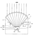
図5に示すように、本第2実施形態では、還元電極12bは、半導体層12aの一面側(図5における上側)から延びるように設けられている。還元電極12bは、略円錐面形状若しくは斜面形状となっており、半導体層12aから離れるほど径が広がっている。
本第2実施形態では、還元電極12bとしてCu、In、Sn等の金属電極、若しくは導電性を備える導電性材料を用いることができる。また、還元電極12bの表面に触媒電極としてPt、NiCo3O4等を設けてもよい。
電解液11は、還元電極12bより下方に存在しているが、還元電極12bより上方には存在していない。このため、半導体層12aにおける還元電極12bが設けられた一面側は、大気中に露出している。したがって、太陽光は半導体層12aにおける一面側の表面に直接照射される。
以上説明した本第2実施形態によれば、上記第1実施形態と同様、集光レンズ14によって太陽光を集光することで半導体層12aで発生する熱エネルギーを、電極12b、12c表面での電極反応に積極的に有効利用できる。
また、本第2実施形態では、半導体層12aから延設されたカソード触媒12b表面で電極反応が進行する。このため、半導体層12aのカソード触媒12bが設けられた一面側(図5の上側)の表面では電極反応が進行せず、半導体層12aの一面側表面が劣化することを抑制できる。
また、本第2実施形態では、大気中に露出している半導体層12aの一面側には太陽光が直接入射する。これにより、半導体層12aにおける太陽光から電気への変換効率を向上させることができる。
(他の実施形態)
本開示発明は上述の実施形態に限定されることなく、本開示の趣旨を逸脱しない範囲内で、以下のように種々変形可能である。また、上記各実施形態は、実施可能な範囲で適宜組み合わせてもよい。
本開示発明は上述の実施形態に限定されることなく、本開示の趣旨を逸脱しない範囲内で、以下のように種々変形可能である。また、上記各実施形態は、実施可能な範囲で適宜組み合わせてもよい。
(1)例えば、集光レンズ14の倍率、焦点、位置あるいは方向を変更可能なレンズ調整機構を設けてもよい。このようなレンズ調整機構で集光レンズ14の倍率、焦点、位置あるいは方向の少なくともいずれかを調整することで、半導体光触媒12が太陽光を吸収した際の温度を調整することが可能となる。
また、レンズ調整機構に加え、半導体光触媒12の温度を検出する温度センサと、温度センサによって検出した半導体光触媒12の温度に基づいてレンズ調整機構を制御する制御装置を設けてもよい。これにより、半導体光触媒12の温度に基づいて集光レンズ14を調整することができ、半導体光触媒12の温度をより適切に制御することが可能となる。
(2)また、電解液11の還元電極12b側にメディエータを含有させてもよい。メディエータは、二酸化炭素還元反応で電子伝達を仲介する化合物である。メディエータとしては、窒素含有芳香族化合物を用いることができる。芳香族化合物は、4n+2個(nは整数)のπ電子を含有する非局在π電子系を有する平面環である。芳香環は、5、6、7、8、9個、又は10個以上の原子によって形成され得る。芳香族化合物は、単環式および縮合環多環式を含んでいる。
窒素含有芳香族化合物は、芳香環の構成原子の1以上がN原子となっている複素芳香族化合物である。窒素含有芳香族化合物は、芳香環の構成原子と結合する1以上の水素が、直鎖または分岐鎖低級アルキル基、ヒドロキシ基、アミノ基、ピリジル基で置換されていてもよい。このようなメディエータを構成する窒素含有芳香族化合物として、イミダゾール、メチルイミダゾール、ジメチルイミダゾール、トリアゾール、ピリジン、ジメチルアミノピリジンを例示できる。
本開示は、実施形態に準拠して記述されたが、本開示は当該実施形態や構造に限定されるものではないと理解される。本開示は、様々な変形例や均等範囲内の変形をも包含する。加えて、様々な組み合わせや形態、さらには、それらに一要素のみ、それ以上、あるいはそれ以下、を含む他の組み合わせや形態をも、本開示の範疇や思想範囲に入るものである。
Claims (5)
- 光を所定の倍率で集光する集光レンズ(14)と、
前記集光レンズによって集光された前記光を吸収して内部光電効果を発生させる半導体層(12a)と、二酸化炭素を還元して炭素化合物を生成する還元電極(12b)と、水を酸化して酸素および水素イオンを生成する酸化電極(12c)とが一体化して構成された半導体光触媒(12)と、を備え、
前記半導体層は、前記光を吸収して熱を発し、
前記半導体層で発生した前記熱が前記還元電極および前記酸化電極に伝えられる人工光合成装置。 - 前記集光レンズによる集光を調整することで、前記半導体層の温度を制御する請求項1に記載の人工光合成装置。
- 前記半導体層の温度が100℃以下となるように、前記集光レンズによる集光が調整されている請求項2に記載の人工光合成装置。
- 前記半導体層は、III-V族半導体によって構成されている請求項1ないし3のいずれか1つに記載の人工光合成装置。
- 電解液(11)と、
前記電解液を収容する容器(10)と、をさらに備え、
前記半導体光触媒は、前記電解液に浸されており、
前記半導体層の一面側に前記還元電極が形成され、前記半導体層の他面側に前記酸化電極が形成されており、
前記還元電極は前記半導体層の一面側の表面から延びるように設けられており、
前記半導体層には前記一面側から光が照射され、
前記半導体層の一面側が大気中に露出している請求項1ないし4のいずれか1つに記載の人工光合成装置。
Applications Claiming Priority (2)
| Application Number | Priority Date | Filing Date | Title |
|---|---|---|---|
| JP2016110987A JP6610442B2 (ja) | 2016-06-02 | 2016-06-02 | 人工光合成装置 |
| JP2016-110987 | 2016-06-02 |
Publications (1)
| Publication Number | Publication Date |
|---|---|
| WO2017208693A1 true WO2017208693A1 (ja) | 2017-12-07 |
Family
ID=60479574
Family Applications (1)
| Application Number | Title | Priority Date | Filing Date |
|---|---|---|---|
| PCT/JP2017/016675 Ceased WO2017208693A1 (ja) | 2016-06-02 | 2017-04-27 | 人工光合成装置 |
Country Status (2)
| Country | Link |
|---|---|
| JP (1) | JP6610442B2 (ja) |
| WO (1) | WO2017208693A1 (ja) |
Citations (4)
| Publication number | Priority date | Publication date | Assignee | Title |
|---|---|---|---|---|
| JP2012036414A (ja) * | 2010-08-03 | 2012-02-23 | Sony Corp | 発電・水素ガス発生装置 |
| JP2014101551A (ja) * | 2012-11-20 | 2014-06-05 | Toshiba Corp | 光化学反応装置 |
| WO2015019553A1 (ja) * | 2013-08-06 | 2015-02-12 | パナソニックIpマネジメント株式会社 | 光化学反応装置用集光装置 |
| JP2015183218A (ja) * | 2014-03-24 | 2015-10-22 | 株式会社東芝 | 光電気化学反応装置 |
-
2016
- 2016-06-02 JP JP2016110987A patent/JP6610442B2/ja active Active
-
2017
- 2017-04-27 WO PCT/JP2017/016675 patent/WO2017208693A1/ja not_active Ceased
Patent Citations (4)
| Publication number | Priority date | Publication date | Assignee | Title |
|---|---|---|---|---|
| JP2012036414A (ja) * | 2010-08-03 | 2012-02-23 | Sony Corp | 発電・水素ガス発生装置 |
| JP2014101551A (ja) * | 2012-11-20 | 2014-06-05 | Toshiba Corp | 光化学反応装置 |
| WO2015019553A1 (ja) * | 2013-08-06 | 2015-02-12 | パナソニックIpマネジメント株式会社 | 光化学反応装置用集光装置 |
| JP2015183218A (ja) * | 2014-03-24 | 2015-10-22 | 株式会社東芝 | 光電気化学反応装置 |
Also Published As
| Publication number | Publication date |
|---|---|
| JP2017214637A (ja) | 2017-12-07 |
| JP6610442B2 (ja) | 2019-11-27 |
Similar Documents
| Publication | Publication Date | Title |
|---|---|---|
| Tournet et al. | III–V semiconductor materials for solar hydrogen production: status and prospects | |
| US4094751A (en) | Photochemical diodes | |
| US10472724B2 (en) | Chemical reaction device | |
| Chandran et al. | Solar-driven sustainability: III–V semiconductor for green energy production technologies | |
| US10378116B2 (en) | Photoelectrochemical reaction device | |
| US9598781B2 (en) | Carbon dioxide reducing method, carbon dioxide reducing cell, and carbon dioxide reducing apparatus | |
| US10233549B2 (en) | Photo-electrochemical reaction device | |
| Navid et al. | On the design and performance of InGaN/Si double-junction photocathodes | |
| Ko et al. | Coupling furfural oxidation for bias-free hydrogen production using crystalline silicon photoelectrodes | |
| Zhou et al. | Nanoengineered kesterite photocathodes: enhancing photoelectrochemical performance for water splitting and beyond | |
| JP6474000B2 (ja) | 二酸化炭素の還元方法、及び二酸化炭素の還元装置 | |
| JP6640686B2 (ja) | 電気化学反応装置 | |
| JP6631467B2 (ja) | 二酸化炭素還元装置 | |
| Miller | Solar hydrogen production by photoelectrochemical water splitting: the promise and challenge | |
| JP6610442B2 (ja) | 人工光合成装置 | |
| Warren et al. | Photoelectrochemical water splitting: silicon photocathodes for hydrogen evolution | |
| Miller et al. | Multijunction approaches to photoelectrochemical water splitting | |
| JP6711334B2 (ja) | 二酸化炭素還元装置 | |
| Mathew et al. | Solar hydrogen production using III-Nitride nanowire photoelectrode | |
| KR810001137B1 (ko) | 광화학 다이오드 | |
| Djellal et al. | Hydrogen production over CuIn3Se5/WO3 hetero-junction | |
| ISHIZUKA | IKEDA SH. | |
| US20230392268A1 (en) | Carbon Dioxide Reduction Device | |
| WO2018116774A1 (ja) | 二酸化炭素還元装置 | |
| JP2017222909A (ja) | 人工光合成装置 |
Legal Events
| Date | Code | Title | Description |
|---|---|---|---|
| 121 | Ep: the epo has been informed by wipo that ep was designated in this application |
Ref document number: 17806252 Country of ref document: EP Kind code of ref document: A1 |
|
| NENP | Non-entry into the national phase |
Ref country code: DE |
|
| 122 | Ep: pct application non-entry in european phase |
Ref document number: 17806252 Country of ref document: EP Kind code of ref document: A1 |