WO2017208642A1 - 樹脂パッケージ - Google Patents
樹脂パッケージ Download PDFInfo
- Publication number
- WO2017208642A1 WO2017208642A1 PCT/JP2017/015081 JP2017015081W WO2017208642A1 WO 2017208642 A1 WO2017208642 A1 WO 2017208642A1 JP 2017015081 W JP2017015081 W JP 2017015081W WO 2017208642 A1 WO2017208642 A1 WO 2017208642A1
- Authority
- WO
- WIPO (PCT)
- Prior art keywords
- resin
- resin package
- semiconductor chip
- package
- semiconductor element
- Prior art date
- Legal status (The legal status is an assumption and is not a legal conclusion. Google has not performed a legal analysis and makes no representation as to the accuracy of the status listed.)
- Ceased
Links
Images


Classifications
-
- G—PHYSICS
- G01—MEASURING; TESTING
- G01P—MEASURING LINEAR OR ANGULAR SPEED, ACCELERATION, DECELERATION, OR SHOCK; INDICATING PRESENCE, ABSENCE, OR DIRECTION, OF MOVEMENT
- G01P15/00—Measuring acceleration; Measuring deceleration; Measuring shock, i.e. sudden change of acceleration
- G01P15/02—Measuring acceleration; Measuring deceleration; Measuring shock, i.e. sudden change of acceleration by making use of inertia forces using solid seismic masses
- G01P15/08—Measuring acceleration; Measuring deceleration; Measuring shock, i.e. sudden change of acceleration by making use of inertia forces using solid seismic masses with conversion into electric or magnetic values
- G01P15/125—Measuring acceleration; Measuring deceleration; Measuring shock, i.e. sudden change of acceleration by making use of inertia forces using solid seismic masses with conversion into electric or magnetic values by capacitive pick-up
-
- H—ELECTRICITY
- H10—SEMICONDUCTOR DEVICES; ELECTRIC SOLID-STATE DEVICES NOT OTHERWISE PROVIDED FOR
- H10W—GENERIC PACKAGES, INTERCONNECTIONS, CONNECTORS OR OTHER CONSTRUCTIONAL DETAILS OF DEVICES COVERED BY CLASS H10
- H10W74/00—Encapsulations, e.g. protective coatings
- H10W74/10—Encapsulations, e.g. protective coatings characterised by their shape or disposition
-
- H—ELECTRICITY
- H10—SEMICONDUCTOR DEVICES; ELECTRIC SOLID-STATE DEVICES NOT OTHERWISE PROVIDED FOR
- H10W—GENERIC PACKAGES, INTERCONNECTIONS, CONNECTORS OR OTHER CONSTRUCTIONAL DETAILS OF DEVICES COVERED BY CLASS H10
- H10W74/00—Encapsulations, e.g. protective coatings
- H10W74/40—Encapsulations, e.g. protective coatings characterised by their materials
-
- H—ELECTRICITY
- H10—SEMICONDUCTOR DEVICES; ELECTRIC SOLID-STATE DEVICES NOT OTHERWISE PROVIDED FOR
- H10W—GENERIC PACKAGES, INTERCONNECTIONS, CONNECTORS OR OTHER CONSTRUCTIONAL DETAILS OF DEVICES COVERED BY CLASS H10
- H10W90/00—Package configurations
-
- H—ELECTRICITY
- H10—SEMICONDUCTOR DEVICES; ELECTRIC SOLID-STATE DEVICES NOT OTHERWISE PROVIDED FOR
- H10W—GENERIC PACKAGES, INTERCONNECTIONS, CONNECTORS OR OTHER CONSTRUCTIONAL DETAILS OF DEVICES COVERED BY CLASS H10
- H10W74/00—Encapsulations, e.g. protective coatings
Definitions
- the present invention relates to a resin package, and more particularly to a resin package having a semiconductor chip inside.
- acceleration sensors and angular velocity sensors mounted on physical quantity sensors detection means using silicon (Si) micromachining technology have become mainstream for the purpose of miniaturization and the like. Specifically, by forming a finely-toothed tooth-like structure body of silicon by microfabrication technology inside the semiconductor chip and applying an inertial force such as acceleration or angular velocity, a minute displacement generated in the comb-tooth-like structure body is obtained. Physical quantities such as acceleration and angular velocity are detected by converting them into electrical signals.
- the linear expansion coefficient between the member such as a semiconductor chip and a wiring board and the resin to be sealed is different.
- members such as semiconductor chips and wiring boards are usually different in size and thickness, and the resin package often has an asymmetric configuration.
- the resin package may be warped and deformed due to a difference in linear expansion coefficient between members or an asymmetry of the structure.
- Patent Document 1 has improved such warpage of a resin package from the viewpoint of flatness required for a terminal portion when the package is mounted. Specifically, in Patent Document 1, the flatness of the entire package is obtained by forming a package shape having a convex arc upward in a portion where a semiconductor chip is mounted and a convex arc downward in other regions. This improves the mountability.
- the semiconductor chip inside the resin package can also be deformed (expansion / shrinkage or warpage).
- a semiconductor chip deform transforms, a stress will arise in a semiconductor chip and this will also produce a displacement also in the comb-tooth-like structure inside a semiconductor chip used as a sensing part. That is, the detection signal is output even in a state where inertial forces such as acceleration and angular velocity are not acting. As a result, the reliability of the sensor is significantly reduced, such as narrowing the detection range of inertial force.
- a sensor in which silicon microfabrication technology is applied to the inertial force detection means needs to have a package structure that does not cause deformation in the sensing portion inside the semiconductor chip even if deformation occurs in the package.
- Patent Document 1 even when the flatness is improved by reducing the warpage of the entire package, the warping of the sensing portion is not necessarily minimized when the semiconductor chip as the sensing portion is provided inside, and the shift of the sensor output is improved. There is a problem of not reaching.
- An object of the present invention is to provide a resin package that suppresses fluctuations in the output signal of a sensor.
- the resin package of the present invention employs the following configuration, for example. That is, in a resin package provided with a semiconductor element, the warpage between the surface on one side and the surface on the other side is opposite in the resin package.
- the semiconductor device of the present invention it is possible to provide a resin package in which fluctuation of the output signal of the sensor is suppressed.
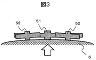
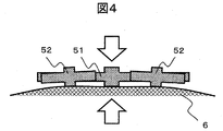
- Example 1 of this invention Schematic plan view of the sensing unit Schematic cross-sectional view of sensing unit affected by warpage in conventional configuration Schematic cross-sectional view of the sensing section affected by warpage in the present invention
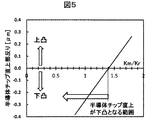
- the figure which showed the relation between coefficient ratio Km / Kr and the warp of the whole package Schematic sectional view of Example 2 of the present invention
- Example 1 will be described.
- FIG. 1 is a diagram showing a schematic cross section and a warped shape of Example 1 of the present invention.
- the resin package 1 has a configuration in which a semiconductor chip 3 having a hollow structure is disposed on a wiring board 2 and one surface (upper surface) thereof and sealed with a resin 4.
- the semiconductor chip 3 has a hollow structure inside, and the hollow part has a sensing part 5 that detects physical quantities such as acceleration and angular velocity.
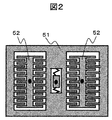
- FIG. 2 is a schematic plan view of the sensing unit 5.
- the sensing unit 5 includes a fixed electrode 51 and a movable electrode 52.
- the fixed electrode 51 and the movable electrode 52 have regions facing each other, and constitute a comb tooth capacity.
- the fixed electrode 51 is fixed to the frame 6 of the semiconductor chip 3, and the movable electrode 52 is fixed to the frame 6 through a spring structure.
- the comb capacity C composed of the fixed electrode 51 and the movable electrode 52 is determined by C ⁇ S / d depending on the distance d between the opposed electrodes and the opposed area S.
- acceleration is applied to the semiconductor chip 3 as a physical quantity
- the movable electrode 52 is displaced in accordance with the applied acceleration, and the comb tooth capacity C is changed by changing the distance d.
- the fixed electrode 51 and the movable electrode 52 are independently drawn to the surface of the semiconductor chip 3 and are electrically connected to the wiring board 2 through the metal thin wire 7, and are connected to the outside of the resin package 1 through the wiring board 2. Electrically connected.
- the wiring board 2 is made of a glass epoxy board (for example, FR4 or FR5), and a predetermined conductor pattern or electrode is formed on the surface or inside thereof.
- a glass epoxy board for example, FR4 or FR5
- the semiconductor chip 3 is mounted on a predetermined portion of the wiring substrate 2 by a bonding material (not shown).
- a bonding material a paste-like bonding material or a film-like bonding material is used. Since the film-like bonding material can maintain a uniform thickness after the members are joined, it is effective in suppressing variations in mounting positions of members (variations in horizontality) and reducing variations in sensor output.
- the electrical connection between the semiconductor chip 3 and the wiring board 2 may be a conductive bump.
- the conductive bump for example, a metal such as gold, silver, copper, tin, and a solder material, or an alloy thereof can be used.
- the process of molding the resin 4 is usually performed at a temperature of 180 ° C.
- Each component is deformed by a temperature difference from 180 ° C. at a temperature around room temperature used in the product stage, and therefore internal stress is generated in the resin package 1.
- the sensing unit 5 changes the facing area S between the fixed electrode 51 and the movable electrode 52 or the inter-electrode distance d as shown in FIG. C changes, and the sensor output shifts even though no physical quantity such as acceleration is applied.
- the resin material used for the wiring board 2 and the resin 4 swells due to moisture absorption. Since the swelling degree of each material due to moisture absorption is different, warping may occur in the entire resin package 1 due to moisture absorption. Then, as in the case of deformation due to temperature change, internal stress is generated in the resin package, the semiconductor chip 3 is also deformed, and when the capacitance C is changed in the sensing unit 5, the sensor output is shifted.
- the direction in which the semiconductor chip 3 is mounted on the wiring board 2 is defined as the upward direction, and the opposite direction is defined as the downward direction.
- the present inventors studied to suppress the output shift by making the warpage of the entire resin package 1 an upward convex shape and by forming a downward convex shape immediately above the semiconductor chip 3. That is, the inventors examined the characteristics of the warp immediately above the semiconductor chip 3 and the warp of the entire resin package 1 to be opposite characteristics (the warp having a downward convex shape with respect to the warp having an upward convex shape).
- FIG. 4 shows a state diagram of the sensing unit 5 in the present embodiment.
- FIG. 5 is a diagram showing the relationship between the coefficient ratio Km / Kr and the warp shape immediately above the semiconductor chip 3.
- the value of warpage is positive, and in the case of a downward convex shape, the value of warpage is negative. From this relationship, it can be seen that when the coefficient ratio Km / Kr is 1.4 or less, the warp immediately above the chip has a downward convex shape.
- the warpage shape of the entire package is determined mainly by the relative relationship between the wiring board 2 and the resin 4, the linear expansion coefficient of the wiring board 2 is ⁇ s, the Young's modulus is Es, and the thickness of the upper part of the hollow portion is Hs.
- FIG. 6 shows the relationship between the coefficient ratio Ks / Kr and the warpage shape of the entire package.
- the value of warpage is positive, and in the case of a downward convex shape, the value of warpage is negative. From this relationship, it can be seen that when the coefficient ratio Km / Kr is 1 or more, the warpage of the entire package becomes an upwardly convex shape. However, if the upward convex shape becomes too strong, the warp immediately above the chip does not become a downward convex shape. Therefore, in FIG. 6, the relationship of the warp shape directly above the semiconductor chip 3 with respect to the coefficient ratio Ks / Kr is also aligned with the right axis. Indicated. It can be seen that the range in which the warp immediately above the semiconductor chip 3 can maintain the downward convex shape with respect to the coefficient ratio Ks / Kr is when the coefficient ratio Ks / Kr is 3 or less.
- the output shift is reduced by suppressing the fluctuation of the capacitance between the electrodes of the semiconductor chip due to the warp generated in the package depending on changes in temperature and humidity, and the fluctuation of the output signal of the sensor is suppressed. It becomes possible to do.
- a semiconductor chip having a hollow structure inside is manufactured by bonding a plurality of wafers by applying a wafer bonding technique. Even in a portion where the bonding area is small, according to the present invention, the semiconductor chip in the compression direction is viewed from above and below. Since the stress acts, the risk of peeling off can be suppressed, and high reliability can be obtained.
- the wiring board 2 is not a glass epoxy board and may be made of various materials such as ceramics. Furthermore, the electrical connection inside the package in the present invention is not a problem even if it is not a fine metal wire, for example, a solder ball.
- Example 2 will be described in detail below.
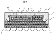
- FIG. 7 is a schematic cross-sectional view of Example 2 of the present invention.
- a control LSI (31) is mounted on a wiring board 2, and two hollow semiconductor chips (32) (33) are further disposed thereon.
- the hollow-structured semiconductor chip detects different physical quantities or becomes a plurality of independent sensors having different detection axes.
- it is effective to apply the through electrode 8 to derive the electrical signal from the sensing unit 5 formed in the hollow structure to the chip surface.
- the through electrode 8 is indispensable to perform deep etching for forming an insulating layer with the surrounding bulk part, and the thickness of the upper part of the hollow part is restricted due to the aspect ratio limitation.
- a BGA Bit Grid Array
- CSP Chip Size Package
- LGA Low-Value Ball
- SOP Small-Value Package
- the chip configuration inside the package is exemplified for the case of two-layer stacking of three chips, but there is no problem even if the number of chips is an arbitrary number, and it may be a multi-layer stacking configuration at all. .
- SYMBOLS 1 Resin package, 2 ... Wiring board, 3 ... Semiconductor chip, 4 ... Resin, 5 ... Sensing part, 51 ... Fixed electrode, 52 ... Movable electrode, 6 ... Frame, 7 ... Metal fine wire, 8 ... Through electrode, 9 ... Solder balls
Landscapes
- Physics & Mathematics (AREA)
- General Physics & Mathematics (AREA)
- Structures Or Materials For Encapsulating Or Coating Semiconductor Devices Or Solid State Devices (AREA)
- Pressure Sensors (AREA)
Abstract
センサの出力信号の変動を抑制した樹脂パッケージを提供すること。 半導体素子を備えた樹脂パッケージにおいて、樹脂パッケージは、一方側の面と他方側の面との反りが逆特性となっている構造。
Description
本発明は、樹脂パッケージに係り、特に、内部に半導体チップを有する樹脂パッケージに関する。
近年、自動車や携帯電話、デジタルカメラなどの安定動作、信頼性向上のため種々の物理量を検出する物理量センサが開発されている。自動車においては、特に加速度センサや角速度センサが横滑り防止や乗員の安全性を向上するための機器(例えばエアバック)の制御用として適用が拡大している。また、物理量センサの自動車への適用では、エンジンルームへの搭載も想定されるため、熱変化や機械的振動などの過酷な環境負荷に耐えることが必要であるとともに、限られたスペースに搭載可能とするため、物理量センサ自体も小型化することが不可欠となっている。
物理量センサに搭載される加速度センサや角速度センサでは、小型化などを目的に、シリコン(Si)の微細加工技術を用いた検出手段が主流となってきている。具体的には、半導体チップ内部に微細加工技術によってシリコンの微細なくし歯状構造体を形成し、加速度や角速度などの慣性力が印加されることによって、くし歯状構造体に生じる微小変位を、電気信号に変換することで加速度や角速度などの物理量を検出している。
そして、このような加速度センサや角速度センサを樹脂封止してパッケージングした樹脂パッケージでは、内部に有する半導体チップや配線基板などの部材と封止する樹脂との線膨張係数が異なっている。また、半導体チップや配線基板などの部材は、通常、サイズや厚さが異なっており、樹脂パッケージは非対称な構成となる場合が多い。このような樹脂パッケージに温度変化が加わると部材間の線膨張係数差や構造の非対称性によって樹脂パッケージには反り変形が生じる場合がある。
このような、樹脂パッケージの反りについて、例えば、特許文献1では、パッケージを実装する際に端子部に求められる平坦性の観点で改善がなされてきた。具体的には、特許文献1では、半導体チップを搭載している部分においては上に凸の弧、それ以外の領域では下に凸の弧となるパッケージ形状にすることによってパッケージ全体としての平坦性を向上し実装性を改善したものである。
しかしながら、樹脂パッケージの反り変形によって、樹脂パッケージの内部にある半導体チップにも変形(膨張収縮や反り)が生じ得る。そして、半導体チップが変形すると半導体チップには応力が生じ、これによってセンシング部となる半導体チップ内部のくし歯状構造体にも変位が生じる。すなわち、加速度や角速度などの慣性力が作用していない状態でも検出信号を出力してしまう。その結果、慣性力の検出範囲を狭めるなどのセンサの信頼性を著しく低下させる要因となる。
従って、シリコンの微細加工技術を慣性力検出手段に適用したセンサでは、パッケージに変形が生じても半導体チップ内部のセンシング部に変形を生じさせないパッケージ構造とすることが必要となる。
特許文献1ではパッケージ全体の反りを小さくして平坦性を向上させても、センシング部である半導体チップを内部に有する場合、センシング部の反りは必ずしも最小とならず、センサ出力のシフトの改善には至らないという課題がある。
本発明の目的は、センサの出力信号の変動を抑制した樹脂パッケージを提供することにある。
上記課題を解決するため、本発明の樹脂パッケージは例えば以下に示す構成を採用する。すなわち、半導体素子を備えた樹脂パッケージにおいて、樹脂パッケージは、一方側の面と他方側の面との反りが逆特性となっている。
本発明の半導体装置によれば、センサの出力信号の変動を抑制した樹脂パッケージを提供することが可能となる。
以下、図面を用いて実施例について詳述する。
まず初めに実施例1について説明する。
図1は本発明の実施例1の模式的断面とその反り形状を示した図である。樹脂パッケージ1は、配線基板2とその一方の面(上面)上に内部に中空構造を有した半導体チップ3を配置し、樹脂4で封止された構成となっている。
半導体チップ3は内部に中空構造を有しており、中空部には加速度や角速度などの物理量を検知するセンシング部5を有している。図2はセンシング部5の模式的な平面図である。センシング部5は固定電極51と可動電極52とからなり、固定電極51と可動電極52は互いに対向する領域を有し、くし歯容量を構成している。固定電極51は半導体チップ3の枠6に固定されており、可動電極52はばね構造を介して枠6に固定される。固定電極51と可動電極52よりなるくし歯容量Cは、対向する電極間の距離dと対向する面積Sによって、C∝S/dによって決まる。半導体チップ3に物理量として例えば加速度が印加されると、印加加速度に応じて可動電極52が変位し、距離dが変化することでくし歯容量Cが変化する。
固定電極51と可動電極52はそれぞれ独立に半導体チップ3の表面に引き出され、金属細線7を介して配線基板2に電気的に接続されており、配線基板2を介して樹脂パッケージ1の外部と電気的に接続される。
配線基板2はガラスエポキシ基板(例えばFR4やFR5)から成り、表面もしくは内部に所定の導体パターンや電極が形成される。
ここで半導体チップ3は配線基板2に接合材(図示はせず。)によって所定の部位に搭載される。接合材にはペースト状接合材やフィルム状接合材が用いられる。フィルム状接合材は、部材接合後の厚さを均一に保てるので、部材の搭載位置ばらつき(水平度のばらつき)を抑制し、センサ出力ばらつきの低減に効果がある。また半導体チップ3と配線基板2との電気的接続は導電性バンプであってもよい。導電性バンプは、例えば金、銀、銅、錫、および半田材料等の金属、あるいはそれらの合金を用いることができる。
上述の樹脂パッケージ1の製造工程において、樹脂4を成形する工程は通常180℃の温度で行われる。各構成部品は、製品段階で使用される室温付近の温度では、180℃からの温度差によってそれぞれに変形するため樹脂パッケージ1には内部応力が発生する。この内部応力によって半導体チップ3に反りが生ずるとセンシング部5において、図3に示したように、固定電極51と可動電極52との対向面積Sあるいは電極間距離dの変化が生じ、くし歯容量Cが変化することになり、加速度等の物理量がまったく印加されていないにもかかわらずセンサ出力がシフトしてしまう。
また配線基板2や樹脂4に用いる樹脂材料は吸湿により膨潤することが知られている。各材料の吸湿による膨潤度合はそれぞれ異なるため、吸湿によって樹脂パッケージ1全体に反りが生じる場合がある。すると温度変化による変形の場合と同様に樹脂パッケージに内部応力が発生し、半導体チップ3にも変形が発生し、センシング部5において容量Cが変化するとセンサ出力がシフトしてしまう。
この構成の樹脂パッケージ1において、配線基板2に対して半導体チップ3を搭載する方向を上方向、その反対方向を下方向と定義する。
ここで本発明者らは、樹脂パッケージ1全体の反りを上凸形状にするとともに、半導体チップ3の直上部においては下凸形状として、出力シフトを抑制することを検討した。すなわち、半導体チップ3の直上部の反りと樹脂パッケージ1全体の反りの特性を逆特性(上凸形状となるような反りに対して下凸形状となるような反り)とすることについて検討した。
図4に本実施例におけるセンシング部5の状態図を示した。チップ直上部の反りを下凸形状とすることによってセンシング部5に下方向への応力が生じ、パッケージ全体の上凸形状によって生じる上方向のセンシング部5への応力を打ち消すことができ、固定電極51と可動電極52との間の対向面積Sおよび電極間距離dが変化する度合いを軽減することができる。そのため電極間容量Cの変化が抑制され、出力シフトを小さくすることができる。
ここでチップ直上部の反り形状は、半導体チップ3と樹脂4との相対関係で支配的に決定される。そのため半導体チップ3の線膨張係数をαm、ヤング率をEm、中空部上部の厚さをHmとしたときに各値の積で決まる係数Km=αm×Em×Hmと、樹脂4の線膨張係数をαr、ヤング率をEr、半導体チップ3の直上部のレジンの厚さをHrとしたときに各値の積で決まる係数Kr=αr×Er×Hrとの係数比Km/Krを考える。
図5は係数比Km/Krと半導体チップ3直上部の反り形状の関係を示した図である。上凸形状の場合は反りの数値は正、下凸形状の場合は反りの数値は負となる。本関係から係数比Km/Krが1.4以下であるときに、チップ直上部の反りが下凸形状になることがわかる。
またパッケージ全体の反り形状は、配線基板2と樹脂4との相対関係で支配的に決まるため、配線基板2の線膨張係数をαs、ヤング率をEs、中空部上部の厚さをHsとしたときに各値の積で決まる係数Ks=αs×Es×Hsと係数Krとの係数比Ks/Krを考える。
図6は係数比Ks/Krとパッケージ全体の反り形状の関係を示した図である。上凸形状の場合は反りの数値は正、下凸形状の場合は反りの数値は負となる。本関係から係数比Km/Krが1以上であるときに、パッケージ全体の反りが上凸形状になることがわかる。ただし上凸形状が強くなり過ぎると、チップ直上部の反りが下凸形状とならなくなるため、図6には係数比Ks/Krに対する半導体チップ3直上部の反り形状の関係も右軸に合せて示した。係数比Ks/Krに対して半導体チップ3直上部の反りが下凸形状を維持できる範囲は、係数比Ks/Krが3以下のときであることが分かる。
以上の構成により、温度や湿度の変化に依存してパッケージに生じた反りによって半導体チップの電極間容量が変動することを抑制されることで出力シフトを小さくし、センサの出力信号の変動を抑制することが可能となる。
また、さらに内部に中空構造をもつ半導体チップはウェハ貼り合せ技術を適用して複数枚のウェハが接合されて製作されるが、接合面積が小さい箇所においても本発明によれば上下から圧縮方向の応力が作用するため、はがれてしまう危険を抑制することができ、高い信頼性を得ることも可能となる。
なお、配線基板2は、ガラスエポキシ基板でなくてもセラミック等各種材料であっても何ら問題ではない。さらに本発明におけるパッケージ内部の電気的接続は金属細線でなくても、たとえば半田ボールであっても何ら問題ではない。
次に実施例2について以下詳述する。
図7は本発明の実施例2の模式的断面を示した図である。図7では、配線基板2上に制御用LSI(31)を搭載し、さらにその上に2ヶの中空構造の半導体チップ(32)(33)を配置した構成となっている。中空構造の半導体チップは互いに異なる物理量を検出したり、互いに異なる検出軸を有している独立した複数のセンサとなる。このような複合センサではチップサイズを小さくすることが望まれるため、中空構造内部に作られるセンシング部5からチップ表面への電気信号の導出は、貫通電極8を適用することが有効な手段となる。貫通電極8を適用する場合、半導体チップの製造工程においては周囲のバルク部との絶縁層形成のために深掘エッチングを実施することが必須となり、そのアスペクト比の制約から中空部上部の厚さにも制約が生じ、厚くすることが困難となる。その結果、樹脂4の変形の影響を受けやすくなり、パッケージ全体反りを小さくしても、半導体チップ上部の形状への影響は十分に小さくできず、センシング部5における容量変化を十分小さくできなくなり、センサ出力の変動量を小さくすることが困難となる。本発明によれば、温度や湿度の影響で樹脂4が変形しても、センシング部5における変形を小さくすることができるため、センサ出力の変動量を最小にすることが可能となる。
本発明は配線基板2の下側に半田ボール9を搭載したBGA(Ball Grid Array)、CSP(Chip Size Package)、半田ボールを搭載しないLGA(Land Grid Array)、金属フレームを有したSOP(Small Outline Package)など各種パッケージに適用することができる。
また本実施例において、パッケージ内部のチップ構成は3チップの2段積層の場合について例示したが、チップ数は任意の数量であっても何ら問題なく、また多段積層構成であっても全く構わない。
1…樹脂パッケージ、2…配線基板、3…半導体チップ、4…樹脂、5…センシング部、51…固定電極、52…可動電極、6…枠、7…金属細線、8…貫通電極、9…半田ボール
Claims (8)
- 半導体素子を備えた樹脂パッケージにおいて、
前記樹脂パッケージは、一方側の面と他方側の面との反りが逆特性となっていることを特徴とする樹脂パッケージ。 - 前記半導体素子は、内部に空間を有する請求項1に記載の樹脂パッケージ。
- 前記樹脂パッケージは、前記半導体素子の空間の下面側が上に凸形状であり上面側が下に凸形状であることを特徴とする請求項2に記載の樹脂パッケージ。
- 前記半導体素子の下面には基板が設けられ、
前記基板が上に凸形状であることを特徴とする請求項3に記載の樹脂パッケージ。 - 前記半導体素子と前記基板と間にはLSIが設けられていることを特徴とする請求項4に記載の樹脂パッケージ。
- 前記半導体素子は前記内部に貫通電極を有する請求項2に記載の樹脂パッケージ。
- 前記半導体素子のヤング率と線膨張係数と厚さとの積をKm、
前記樹脂のヤング率と線膨張係数と前記半導体素子上の樹脂の厚さとの積をKrとすると、
Km/Kr≦1.4であることを特徴とする請求項1に記載の樹脂パッケージ。 - 前記樹脂のヤング率と線膨張係数と前記半導体素子上の樹脂の厚さとの積をKr、
前記基板のヤング率と線膨張係数と厚さとの積をKsとしたとき、
1≦Ks/Kr≦3であることを特徴とする請求項4に記載の樹脂パッケージ。
Priority Applications (1)
| Application Number | Priority Date | Filing Date | Title |
|---|---|---|---|
| JP2018520701A JP6678236B2 (ja) | 2016-05-31 | 2017-04-13 | 樹脂パッケージ |
Applications Claiming Priority (2)
| Application Number | Priority Date | Filing Date | Title |
|---|---|---|---|
| JP2016-108092 | 2016-05-31 | ||
| JP2016108092 | 2016-05-31 |
Publications (1)
| Publication Number | Publication Date |
|---|---|
| WO2017208642A1 true WO2017208642A1 (ja) | 2017-12-07 |
Family
ID=60478264
Family Applications (1)
| Application Number | Title | Priority Date | Filing Date |
|---|---|---|---|
| PCT/JP2017/015081 Ceased WO2017208642A1 (ja) | 2016-05-31 | 2017-04-13 | 樹脂パッケージ |
Country Status (2)
| Country | Link |
|---|---|
| JP (1) | JP6678236B2 (ja) |
| WO (1) | WO2017208642A1 (ja) |
Citations (3)
| Publication number | Priority date | Publication date | Assignee | Title |
|---|---|---|---|---|
| JP2003100958A (ja) * | 2001-09-25 | 2003-04-04 | Mitsubishi Electric Corp | 半導体装置 |
| JP2007173870A (ja) * | 1997-10-15 | 2007-07-05 | Toshiba Corp | 半導体装置および半導体装置の製造方法 |
| JP2012114276A (ja) * | 2010-11-25 | 2012-06-14 | Murata Mfg Co Ltd | 樹脂封止型モジュールおよびその製造方法 |
Family Cites Families (1)
| Publication number | Priority date | Publication date | Assignee | Title |
|---|---|---|---|---|
| JP5978170B2 (ja) * | 2013-06-28 | 2016-08-24 | 日立オートモティブシステムズ株式会社 | トランスファーモールド型センサ装置 |
-
2017
- 2017-04-13 JP JP2018520701A patent/JP6678236B2/ja not_active Expired - Fee Related
- 2017-04-13 WO PCT/JP2017/015081 patent/WO2017208642A1/ja not_active Ceased
Patent Citations (3)
| Publication number | Priority date | Publication date | Assignee | Title |
|---|---|---|---|---|
| JP2007173870A (ja) * | 1997-10-15 | 2007-07-05 | Toshiba Corp | 半導体装置および半導体装置の製造方法 |
| JP2003100958A (ja) * | 2001-09-25 | 2003-04-04 | Mitsubishi Electric Corp | 半導体装置 |
| JP2012114276A (ja) * | 2010-11-25 | 2012-06-14 | Murata Mfg Co Ltd | 樹脂封止型モジュールおよびその製造方法 |
Also Published As
| Publication number | Publication date |
|---|---|
| JP6678236B2 (ja) | 2020-04-08 |
| JPWO2017208642A1 (ja) | 2019-02-07 |
Similar Documents
| Publication | Publication Date | Title |
|---|---|---|
| JP5978170B2 (ja) | トランスファーモールド型センサ装置 | |
| US9885626B2 (en) | Micromechanical sensor system and corresponding manufacturing method | |
| JP4973443B2 (ja) | センサ装置 | |
| US20160185593A1 (en) | Wafer level package for a mems sensor device and corresponding manufacturing process | |
| EP3267486B1 (en) | Sensor package structure | |
| CN102458054A (zh) | 制造电路的方法和电路 | |
| CN111785713A (zh) | 集成加速度传感器和磁传感器的封装结构及其封装方法 | |
| US20170088417A1 (en) | Electronic device and manufacturing method thereof | |
| JP2005127750A (ja) | 半導体センサおよびその製造方法 | |
| EP2994412B1 (en) | A microelectromechanical device and a method of manufacturing | |
| CN212434621U (zh) | 集成加速度传感器和磁传感器的封装结构 | |
| CN1550783A (zh) | 电容型力学量传感器 | |
| JP2010085143A (ja) | 加速度センサー | |
| JP6678236B2 (ja) | 樹脂パッケージ | |
| JP7512785B2 (ja) | 電子装置 | |
| US20150048463A1 (en) | Package device for microelectromechanical inertial sensor | |
| JP7708601B2 (ja) | Memsモジュール及びその製造方法 | |
| JP7542738B2 (ja) | 気密パッケージ素子および素子モジュール | |
| JP6416704B2 (ja) | 樹脂封止型センサ装置 | |
| JP2010181243A (ja) | 容量式力学量センサ装置の製造方法 | |
| JP5033045B2 (ja) | 半導体素子の実装構造 | |
| JP2010008123A (ja) | センサモジュール | |
| JP2007322191A (ja) | 半導体加速度センサ | |
| JP2024027877A (ja) | Memsモジュール | |
| CN101253411A (zh) | 加速度传感器装置及传感器装置 |
Legal Events
| Date | Code | Title | Description |
|---|---|---|---|
| WWE | Wipo information: entry into national phase |
Ref document number: 2018520701 Country of ref document: JP |
|
| NENP | Non-entry into the national phase |
Ref country code: DE |
|
| 121 | Ep: the epo has been informed by wipo that ep was designated in this application |
Ref document number: 17806202 Country of ref document: EP Kind code of ref document: A1 |
|
| 122 | Ep: pct application non-entry in european phase |
Ref document number: 17806202 Country of ref document: EP Kind code of ref document: A1 |